WO2017217308A1 - Electronic component, vibration plate, electronic device, and method for manufacturing electronic components - Google Patents
Electronic component, vibration plate, electronic device, and method for manufacturing electronic components Download PDFInfo
- Publication number
- WO2017217308A1 WO2017217308A1 PCT/JP2017/021254 JP2017021254W WO2017217308A1 WO 2017217308 A1 WO2017217308 A1 WO 2017217308A1 JP 2017021254 W JP2017021254 W JP 2017021254W WO 2017217308 A1 WO2017217308 A1 WO 2017217308A1
- Authority
- WO
- WIPO (PCT)
- Prior art keywords
- main surface
- insulating base
- base material
- insulating
- coil
- Prior art date
Links
- 238000004519 manufacturing process Methods 0.000 title claims description 33
- 238000000034 method Methods 0.000 title claims description 29
- 239000004020 conductor Substances 0.000 claims abstract description 234
- 239000000758 substrate Substances 0.000 claims abstract description 83
- 238000010030 laminating Methods 0.000 claims abstract description 20
- 238000004804 winding Methods 0.000 claims abstract description 13
- 238000009413 insulation Methods 0.000 claims abstract description 11
- 239000000463 material Substances 0.000 claims description 433
- 230000008569 process Effects 0.000 claims description 19
- 229920005992 thermoplastic resin Polymers 0.000 claims description 16
- 230000015572 biosynthetic process Effects 0.000 claims description 12
- 238000010438 heat treatment Methods 0.000 claims description 11
- 238000003825 pressing Methods 0.000 claims description 7
- 238000003475 lamination Methods 0.000 abstract 1
- 239000010410 layer Substances 0.000 description 172
- 239000011229 interlayer Substances 0.000 description 22
- 230000000694 effects Effects 0.000 description 20
- 229920000106 Liquid crystal polymer Polymers 0.000 description 10
- 239000004977 Liquid-crystal polymers (LCPs) Substances 0.000 description 10
- 238000000926 separation method Methods 0.000 description 10
- 238000005304 joining Methods 0.000 description 8
- RYGMFSIKBFXOCR-UHFFFAOYSA-N Copper Chemical compound [Cu] RYGMFSIKBFXOCR-UHFFFAOYSA-N 0.000 description 7
- 229920001187 thermosetting polymer Polymers 0.000 description 7
- 230000000052 comparative effect Effects 0.000 description 6
- 239000011888 foil Substances 0.000 description 6
- 239000002184 metal Substances 0.000 description 6
- 229910052751 metal Inorganic materials 0.000 description 6
- 239000012141 concentrate Substances 0.000 description 4
- 229910000679 solder Inorganic materials 0.000 description 4
- 239000004696 Poly ether ether ketone Substances 0.000 description 3
- 239000000853 adhesive Substances 0.000 description 3
- 230000001070 adhesive effect Effects 0.000 description 3
- 239000003990 capacitor Substances 0.000 description 3
- 238000002844 melting Methods 0.000 description 3
- 230000008018 melting Effects 0.000 description 3
- 238000000059 patterning Methods 0.000 description 3
- 238000000206 photolithography Methods 0.000 description 3
- 229920002530 polyetherether ketone Polymers 0.000 description 3
- 229920005989 resin Polymers 0.000 description 3
- 239000011347 resin Substances 0.000 description 3
- 239000004593 Epoxy Substances 0.000 description 2
- 230000008859 change Effects 0.000 description 2
- 230000004907 flux Effects 0.000 description 2
- 230000012447 hatching Effects 0.000 description 2
- 230000001678 irradiating effect Effects 0.000 description 2
- 238000012986 modification Methods 0.000 description 2
- 230000004048 modification Effects 0.000 description 2
- 230000000704 physical effect Effects 0.000 description 2
- 238000004026 adhesive bonding Methods 0.000 description 1
- 239000012790 adhesive layer Substances 0.000 description 1
- 229910045601 alloy Inorganic materials 0.000 description 1
- 239000000956 alloy Substances 0.000 description 1
- 239000000919 ceramic Substances 0.000 description 1
- 239000003795 chemical substances by application Substances 0.000 description 1
- 229910052802 copper Inorganic materials 0.000 description 1
- 230000007423 decrease Effects 0.000 description 1
- 238000006073 displacement reaction Methods 0.000 description 1
- 239000011521 glass Substances 0.000 description 1
- 229910052750 molybdenum Inorganic materials 0.000 description 1
- 229910052759 nickel Inorganic materials 0.000 description 1
- 230000002093 peripheral effect Effects 0.000 description 1
- 229910052709 silver Inorganic materials 0.000 description 1
- 229910052718 tin Inorganic materials 0.000 description 1
Images


Classifications
-
- H—ELECTRICITY
- H01—ELECTRIC ELEMENTS
- H01F—MAGNETS; INDUCTANCES; TRANSFORMERS; SELECTION OF MATERIALS FOR THEIR MAGNETIC PROPERTIES
- H01F17/00—Fixed inductances of the signal type
- H01F17/0006—Printed inductances
-
- H—ELECTRICITY
- H01—ELECTRIC ELEMENTS
- H01F—MAGNETS; INDUCTANCES; TRANSFORMERS; SELECTION OF MATERIALS FOR THEIR MAGNETIC PROPERTIES
- H01F17/00—Fixed inductances of the signal type
- H01F17/0006—Printed inductances
- H01F17/0013—Printed inductances with stacked layers
-
- H—ELECTRICITY
- H01—ELECTRIC ELEMENTS
- H01F—MAGNETS; INDUCTANCES; TRANSFORMERS; SELECTION OF MATERIALS FOR THEIR MAGNETIC PROPERTIES
- H01F27/00—Details of transformers or inductances, in general
- H01F27/06—Mounting, supporting or suspending transformers, reactors or choke coils not being of the signal type
-
- H—ELECTRICITY
- H01—ELECTRIC ELEMENTS
- H01F—MAGNETS; INDUCTANCES; TRANSFORMERS; SELECTION OF MATERIALS FOR THEIR MAGNETIC PROPERTIES
- H01F27/00—Details of transformers or inductances, in general
- H01F27/28—Coils; Windings; Conductive connections
- H01F27/2804—Printed windings
-
- H—ELECTRICITY
- H01—ELECTRIC ELEMENTS
- H01F—MAGNETS; INDUCTANCES; TRANSFORMERS; SELECTION OF MATERIALS FOR THEIR MAGNETIC PROPERTIES
- H01F27/00—Details of transformers or inductances, in general
- H01F27/28—Coils; Windings; Conductive connections
- H01F27/29—Terminals; Tapping arrangements for signal inductances
- H01F27/292—Surface mounted devices
-
- H—ELECTRICITY
- H01—ELECTRIC ELEMENTS
- H01F—MAGNETS; INDUCTANCES; TRANSFORMERS; SELECTION OF MATERIALS FOR THEIR MAGNETIC PROPERTIES
- H01F41/00—Apparatus or processes specially adapted for manufacturing or assembling magnets, inductances or transformers; Apparatus or processes specially adapted for manufacturing materials characterised by their magnetic properties
- H01F41/02—Apparatus or processes specially adapted for manufacturing or assembling magnets, inductances or transformers; Apparatus or processes specially adapted for manufacturing materials characterised by their magnetic properties for manufacturing cores, coils, or magnets
- H01F41/04—Apparatus or processes specially adapted for manufacturing or assembling magnets, inductances or transformers; Apparatus or processes specially adapted for manufacturing materials characterised by their magnetic properties for manufacturing cores, coils, or magnets for manufacturing coils
- H01F41/041—Printed circuit coils
-
- H—ELECTRICITY
- H01—ELECTRIC ELEMENTS
- H01F—MAGNETS; INDUCTANCES; TRANSFORMERS; SELECTION OF MATERIALS FOR THEIR MAGNETIC PROPERTIES
- H01F7/00—Magnets
- H01F7/06—Electromagnets; Actuators including electromagnets
- H01F7/08—Electromagnets; Actuators including electromagnets with armatures
-
- H—ELECTRICITY
- H05—ELECTRIC TECHNIQUES NOT OTHERWISE PROVIDED FOR
- H05K—PRINTED CIRCUITS; CASINGS OR CONSTRUCTIONAL DETAILS OF ELECTRIC APPARATUS; MANUFACTURE OF ASSEMBLAGES OF ELECTRICAL COMPONENTS
- H05K1/00—Printed circuits
- H05K1/16—Printed circuits incorporating printed electric components, e.g. printed resistor, capacitor, inductor
- H05K1/165—Printed circuits incorporating printed electric components, e.g. printed resistor, capacitor, inductor incorporating printed inductors
-
- H—ELECTRICITY
- H01—ELECTRIC ELEMENTS
- H01F—MAGNETS; INDUCTANCES; TRANSFORMERS; SELECTION OF MATERIALS FOR THEIR MAGNETIC PROPERTIES
- H01F17/00—Fixed inductances of the signal type
- H01F17/0006—Printed inductances
- H01F2017/0046—Printed inductances with a conductive path having a bridge
-
- H—ELECTRICITY
- H01—ELECTRIC ELEMENTS
- H01F—MAGNETS; INDUCTANCES; TRANSFORMERS; SELECTION OF MATERIALS FOR THEIR MAGNETIC PROPERTIES
- H01F17/00—Fixed inductances of the signal type
- H01F17/0006—Printed inductances
- H01F2017/0073—Printed inductances with a special conductive pattern, e.g. flat spiral
-
- H—ELECTRICITY
- H01—ELECTRIC ELEMENTS
- H01F—MAGNETS; INDUCTANCES; TRANSFORMERS; SELECTION OF MATERIALS FOR THEIR MAGNETIC PROPERTIES
- H01F27/00—Details of transformers or inductances, in general
- H01F27/28—Coils; Windings; Conductive connections
- H01F27/2804—Printed windings
- H01F2027/2809—Printed windings on stacked layers
-
- H—ELECTRICITY
- H05—ELECTRIC TECHNIQUES NOT OTHERWISE PROVIDED FOR
- H05K—PRINTED CIRCUITS; CASINGS OR CONSTRUCTIONAL DETAILS OF ELECTRIC APPARATUS; MANUFACTURE OF ASSEMBLAGES OF ELECTRICAL COMPONENTS
- H05K1/00—Printed circuits
- H05K1/18—Printed circuits structurally associated with non-printed electric components
- H05K1/181—Printed circuits structurally associated with non-printed electric components associated with surface mounted components
-
- H—ELECTRICITY
- H05—ELECTRIC TECHNIQUES NOT OTHERWISE PROVIDED FOR
- H05K—PRINTED CIRCUITS; CASINGS OR CONSTRUCTIONAL DETAILS OF ELECTRIC APPARATUS; MANUFACTURE OF ASSEMBLAGES OF ELECTRICAL COMPONENTS
- H05K2201/00—Indexing scheme relating to printed circuits covered by H05K1/00
- H05K2201/09—Shape and layout
- H05K2201/09009—Substrate related
- H05K2201/09036—Recesses or grooves in insulating substrate
-
- H—ELECTRICITY
- H05—ELECTRIC TECHNIQUES NOT OTHERWISE PROVIDED FOR
- H05K—PRINTED CIRCUITS; CASINGS OR CONSTRUCTIONAL DETAILS OF ELECTRIC APPARATUS; MANUFACTURE OF ASSEMBLAGES OF ELECTRICAL COMPONENTS
- H05K2201/00—Indexing scheme relating to printed circuits covered by H05K1/00
- H05K2201/09—Shape and layout
- H05K2201/09145—Edge details
- H05K2201/09154—Bevelled, chamferred or tapered edge
-
- H—ELECTRICITY
- H05—ELECTRIC TECHNIQUES NOT OTHERWISE PROVIDED FOR
- H05K—PRINTED CIRCUITS; CASINGS OR CONSTRUCTIONAL DETAILS OF ELECTRIC APPARATUS; MANUFACTURE OF ASSEMBLAGES OF ELECTRICAL COMPONENTS
- H05K2201/00—Indexing scheme relating to printed circuits covered by H05K1/00
- H05K2201/09—Shape and layout
- H05K2201/09818—Shape or layout details not covered by a single group of H05K2201/09009 - H05K2201/09809
- H05K2201/09827—Tapered, e.g. tapered hole, via or groove
-
- H—ELECTRICITY
- H05—ELECTRIC TECHNIQUES NOT OTHERWISE PROVIDED FOR
- H05K—PRINTED CIRCUITS; CASINGS OR CONSTRUCTIONAL DETAILS OF ELECTRIC APPARATUS; MANUFACTURE OF ASSEMBLAGES OF ELECTRICAL COMPONENTS
- H05K2201/00—Indexing scheme relating to printed circuits covered by H05K1/00
- H05K2201/10—Details of components or other objects attached to or integrated in a printed circuit board
- H05K2201/10007—Types of components
- H05K2201/10083—Electromechanical or electro-acoustic component, e.g. microphone
-
- H—ELECTRICITY
- H05—ELECTRIC TECHNIQUES NOT OTHERWISE PROVIDED FOR
- H05K—PRINTED CIRCUITS; CASINGS OR CONSTRUCTIONAL DETAILS OF ELECTRIC APPARATUS; MANUFACTURE OF ASSEMBLAGES OF ELECTRICAL COMPONENTS
- H05K2201/00—Indexing scheme relating to printed circuits covered by H05K1/00
- H05K2201/10—Details of components or other objects attached to or integrated in a printed circuit board
- H05K2201/10613—Details of electrical connections of non-printed components, e.g. special leads
- H05K2201/10954—Other details of electrical connections
- H05K2201/10977—Encapsulated connections
-
- H—ELECTRICITY
- H05—ELECTRIC TECHNIQUES NOT OTHERWISE PROVIDED FOR
- H05K—PRINTED CIRCUITS; CASINGS OR CONSTRUCTIONAL DETAILS OF ELECTRIC APPARATUS; MANUFACTURE OF ASSEMBLAGES OF ELECTRICAL COMPONENTS
- H05K3/00—Apparatus or processes for manufacturing printed circuits
- H05K3/0011—Working of insulating substrates or insulating layers
- H05K3/0044—Mechanical working of the substrate, e.g. drilling or punching
- H05K3/0052—Depaneling, i.e. dividing a panel into circuit boards; Working of the edges of circuit boards
-
- H—ELECTRICITY
- H05—ELECTRIC TECHNIQUES NOT OTHERWISE PROVIDED FOR
- H05K—PRINTED CIRCUITS; CASINGS OR CONSTRUCTIONAL DETAILS OF ELECTRIC APPARATUS; MANUFACTURE OF ASSEMBLAGES OF ELECTRICAL COMPONENTS
- H05K3/00—Apparatus or processes for manufacturing printed circuits
- H05K3/46—Manufacturing multilayer circuits
- H05K3/4611—Manufacturing multilayer circuits by laminating two or more circuit boards
- H05K3/4626—Manufacturing multilayer circuits by laminating two or more circuit boards characterised by the insulating layers or materials
- H05K3/4632—Manufacturing multilayer circuits by laminating two or more circuit boards characterised by the insulating layers or materials laminating thermoplastic or uncured resin sheets comprising printed circuits without added adhesive materials between the sheets
Abstract
An electronic component (101) comprises an insulation substrate (10) having a first main surface (VS1) that serves as a mounting surface, a coil that is formed on the insulation substrate (3), and mounting electrodes (P1, P2) that are connected to the coil (3) formed on the first main surface (VS1). The insulation substrate (10) is formed by laminating a plurality of insulation substrate layers (11, 12, 13). The coil (3) is configured with a coil conductor (31) formed in the insulation substrate (12), and has a winding axis (AX) in the direction of lamination (the z-axis direction) of the plurality of insulation substrate layers (11, 12, 13). The area of the first main surface (VS1) differs from the area of the first main surface (VS1) in a cross-section parallel to the first main surface (VS1) (the cross-section of the XY plane), and is smaller than the area of the cross-section closest to the first main surface (VS1) (e.g., the interface between the insulation substrate layer (12) and the insulation substrate layer (13)).
Description
本発明は、電子部品に関し、特に積層体にコイルが形成された電子部品および振動板と、その電子部品を備える電子機器、さらには上記電子部品の製造方法に関する。
The present invention relates to an electronic component, and more particularly to an electronic component and a diaphragm in which a coil is formed in a laminated body, an electronic device including the electronic component, and a method for manufacturing the electronic component.
従来、複数の絶縁基材層を積層してなる絶縁基材にコイルが形成された各種電子部品が知られている。例えば、特許文献1には、複数の絶縁基材層の積層方法に巻回軸を有し、絶縁基材の実装面のみに実装電極が形成された電子部品が開示されている。このような電子部品は実装基板等(以下、「他の部材」)に実装される。
Conventionally, various electronic components in which a coil is formed on an insulating base material formed by laminating a plurality of insulating base material layers are known. For example, Patent Document 1 discloses an electronic component having a winding shaft in a method for laminating a plurality of insulating base layers and having mounting electrodes formed only on the mounting surface of the insulating base. Such an electronic component is mounted on a mounting substrate or the like (hereinafter referred to as “other member”).
しかし、上記構成の電子部品では、実装面に大きな実装電極が形成されていると、この実装電極がコイルを通る磁束を妨げることがある。そこで、コイルを通る磁束が妨げられるのを抑制するため、実装電極の面積を小さくする構成が考えられる。しかしながら、そのような実装電極を、はんだ等の導電性接合材を介して、他の部材に形成される導体パターン等に接合する場合、実装電極の面積は小さいため、他の部材への十分な接合強度が確保できない虞がある。
However, in the electronic component having the above configuration, if a large mounting electrode is formed on the mounting surface, the mounting electrode may interfere with the magnetic flux passing through the coil. Therefore, in order to suppress the magnetic flux passing through the coil from being obstructed, a configuration in which the area of the mounting electrode is reduced can be considered. However, when such a mounting electrode is bonded to a conductor pattern or the like formed on another member via a conductive bonding material such as solder, the area of the mounting electrode is small. There is a possibility that the bonding strength cannot be secured.
また、上記構成を振動板に応用することも考えられる。上記の電子部品と同様に、この振動板は、他の部材に接続するために形成された実装電極を有する。上記振動板が振動する際、振動板と他の部材に接合される部分(以下、「接合部」)には、応力がかかる。そのため、他の部材に対して振動板の実装電極を導電性接合材のみで接合した場合には、絶縁基材と導電性接合材との界面に応力が集中し、振動板が他の部材から剥離しやすくなる虞がある。
It is also conceivable to apply the above configuration to the diaphragm. Similar to the electronic component described above, the diaphragm has a mounting electrode formed for connection to another member. When the diaphragm vibrates, stress is applied to a portion (hereinafter, “joined portion”) joined to the diaphragm and another member. Therefore, when the mounting electrode of the diaphragm is bonded to another member with only the conductive bonding material, stress concentrates on the interface between the insulating base material and the conductive bonding material, and the vibration plate is separated from the other member. There is a risk of easy peeling.
これに対し、電子部品および振動板を他の部材に実装する場合、または振動板を他の部材に接合する場合に、絶縁性接合材(アンダーフィル等)を用いて実装電極以外の実装面や接合部を、他の部材に接合(固着)する方法が考えられる。
In contrast, when mounting an electronic component and a diaphragm on another member, or when joining a diaphragm to another member, an insulating bonding material (such as underfill) is used to mount a mounting surface other than the mounting electrode. A method of joining (adhering) the joining portion to another member is conceivable.
しかし、上述したような接合方法でも、絶縁基材を構成する絶縁基材層と絶縁性接合材との間(または、絶縁基材層と他の部材との間)の接合は異種材同士の接合であるため、十分な接合強度が確保できず、電子部品または振動板が他の部材から脱落する虞もある。
However, even in the joining method as described above, joining between the insulating base material layer and the insulating joining material constituting the insulating base material (or between the insulating base material layer and another member) is performed between different materials. Due to the bonding, sufficient bonding strength cannot be ensured, and the electronic component or the diaphragm may fall off from other members.
本発明の目的は、導電性接合材および絶縁性接合材を用いて他の部材に実装する電子部品および振動板において、他の部材に対する十分な接合強度を容易に確保できる電子部品および振動板、この電子部品が実装された他の部材を備える電子機器を提供することにある。また、本発明の目的は、上記電子部品の製造方法を提供することにある。
An object of the present invention is to provide an electronic component and a diaphragm that can easily ensure sufficient bonding strength to other members in an electronic component and a diaphragm that are mounted on another member using a conductive bonding material and an insulating bonding material, An object of the present invention is to provide an electronic device including another member on which the electronic component is mounted. Moreover, the objective of this invention is providing the manufacturing method of the said electronic component.
(1)本発明の電子部品は、
実装面である第1主面を有し、複数の絶縁基材層を積層して形成される絶縁基材と、
前記絶縁基材層に形成されるコイル導体を含んで構成され、前記複数の絶縁基材層の積層方向に巻回軸を有するコイルと、
前記第1主面に形成され、前記コイルに接続される実装電極と、
を備え、
前記第1主面の面積は、前記第1主面に平行な断面のうち、前記第1主面の面積とは異なり、且つ、前記第1主面に最も近い断面の面積よりも小さいことを特徴とする。 (1) The electronic component of the present invention
An insulating substrate having a first main surface that is a mounting surface and formed by laminating a plurality of insulating substrate layers;
A coil including a coil conductor formed on the insulating base layer, and a coil having a winding axis in the stacking direction of the plurality of insulating base layers;
A mounting electrode formed on the first main surface and connected to the coil;
With
The area of the first main surface is different from the area of the first main surface among the cross sections parallel to the first main surface and is smaller than the area of the cross section closest to the first main surface. Features.
この構成により、絶縁性接合材を含めた電子部品の実装面積を大きくすることなく、電子部品と絶縁性接合材との接合強度を高めることができ、実装基板等に対する接合信頼性を高めた電子部品を実現できる。
With this configuration, it is possible to increase the bonding strength between the electronic component and the insulating bonding material without increasing the mounting area of the electronic component including the insulating bonding material, and to improve the bonding reliability with respect to the mounting substrate. Parts can be realized.
(2)上記(1)において、前記コイル導体の数は複数であり、複数の前記コイル導体は、前記複数の絶縁基材層のうち2つ以上の絶縁基材層にそれぞれ形成されることが好ましい。この構成により、所定の巻回数およびインダクタンスを有するコイルを備える電子部品を実現できる。
(2) In the above (1), the number of the coil conductors is plural, and the plurality of coil conductors are respectively formed on two or more insulating base material layers among the plurality of insulating base material layers. preferable. With this configuration, an electronic component including a coil having a predetermined number of turns and an inductance can be realized.
(3)上記(1)または(2)において、前記絶縁基材は、前記第1主面の外縁部に形成される切り欠き部を有していてもよい。
(3) In the above (1) or (2), the insulating base material may have a notch formed in an outer edge portion of the first main surface.
(4)上記(1)から(3)のいずれかにおいて、前記第1主面のうち前記実装電極が形成されていない電極非形成部に、凹凸部が形成されていることが好ましい。この構成により、電極非形成部に凹凸部が形成されていない場合に比べて、実装基板への実装状態で絶縁性接合材に接する電極非形成部の表面積が大きくなるため、絶縁基材と絶縁性接合材との間の接合強度はさらに高まる。
(4) In any one of the above (1) to (3), it is preferable that an uneven portion is formed in an electrode non-formed portion where the mounting electrode is not formed in the first main surface. This configuration increases the surface area of the electrode non-forming portion that is in contact with the insulating bonding material when mounted on the mounting substrate as compared to the case where the uneven portion is not formed on the electrode non-forming portion. The bonding strength between the adhesive bonding material is further increased.
(5)本発明の振動板は、
電磁力によって振動するものであって、
可撓性を有し、配線導体が形成された支持フィルムと、
導電性接合材および絶縁性接合材を介して、前記支持フィルムに接合される電子部品と、
を備え、
前記電子部品は、
実装面である第1主面を有し、複数の絶縁基材層を積層して形成される絶縁基材と、
前記絶縁基材層に形成されるコイル導体を含んで構成されるコイルと、
前記第1主面に形成され、前記コイルに接続される実装電極と、
を有し、
前記第1主面の面積は、前記第1主面に平行な断面のうち、前記第1主面の面積とは異なり、且つ、前記第1主面に最も近い断面の面積よりも小さいことを特徴とする。 (5) The diaphragm of the present invention is
It vibrates by electromagnetic force,
A support film having flexibility and having a wiring conductor formed thereon;
An electronic component bonded to the support film via a conductive bonding material and an insulating bonding material;
With
The electronic component is
An insulating substrate having a first main surface that is a mounting surface and formed by laminating a plurality of insulating substrate layers;
A coil configured to include a coil conductor formed on the insulating base layer;
A mounting electrode formed on the first main surface and connected to the coil;
Have
The area of the first main surface is different from the area of the first main surface among the cross sections parallel to the first main surface and is smaller than the area of the cross section closest to the first main surface. Features.
振動板を導電性接合材のみを用いて支持フィルムに接合した場合、振動時に振動板の実装電極と導電性接合材との界面に応力が集中して、振動板が支持フィルムから剥離しやすくなる。また、振動板が振動を繰り返すと、絶縁基材と支持フィルムとの界面に応力が生じて、電極非形成部と絶縁性接合材との界面で剥離が起こりやすくなる。一方、この構成によれば、絶縁基材の電極非形成部のみが絶縁性接合材を介して支持フィルムに接合される場合に比べて、絶縁基材が絶縁性接合材に接する面積は大きくなり、絶縁基材と絶縁性接合材との間の接合強度が高まる。したがって、絶縁基材と絶縁性接合材の界面の剥離が抑制され、支持フィルムに対する接合信頼性を高めた振動板を実現できる。
When the diaphragm is bonded to the support film using only the conductive bonding material, stress concentrates on the interface between the mounting electrode of the vibration plate and the conductive bonding material during vibration, and the vibration plate is easily peeled off from the support film. . Further, when the vibration plate repeatedly vibrates, stress is generated at the interface between the insulating base material and the support film, and peeling is likely to occur at the interface between the electrode non-formed portion and the insulating bonding material. On the other hand, according to this configuration, the area where the insulating base material is in contact with the insulating bonding material is larger than when only the electrode non-forming portion of the insulating base material is bonded to the support film via the insulating bonding material. The bonding strength between the insulating substrate and the insulating bonding material is increased. Therefore, peeling of the interface between the insulating base material and the insulating bonding material is suppressed, and a diaphragm with improved bonding reliability to the support film can be realized.
(6)上記(5)において、前記絶縁基材は、前記第1主面の外縁部に形成される切り欠き部を有していてもよい。
(6) In the above (5), the insulating base material may have a notch formed in an outer edge portion of the first main surface.
(7)本発明の振動板は、
電磁力によって振動するものであって、
第1主面と、振動する振動部と、他の部材に固定される支持部と、を有し、複数の絶縁基材層を積層して形成される絶縁基材と、
前記絶縁基材層に形成されるコイル導体を含んで構成されるコイルと、
前記第1主面に形成され、前記コイルに接続される実装電極と、
を備え、
前記第1主面の面積は、前記第1主面に平行な断面のうち、前記第1主面の面積とは異なり、且つ、前記第1主面に最も近い断面の面積よりも小さいことを特徴とする。 (7) The diaphragm of the present invention is
It vibrates by electromagnetic force,
An insulating base material that has a first main surface, a vibrating part that vibrates, and a support part that is fixed to another member, and is formed by laminating a plurality of insulating base material layers;
A coil configured to include a coil conductor formed on the insulating base layer;
A mounting electrode formed on the first main surface and connected to the coil;
With
The area of the first main surface is different from the area of the first main surface among the cross sections parallel to the first main surface and is smaller than the area of the cross section closest to the first main surface. Features.
振動板が振動する際、支持部の接合部には応力がかかる。他の部材に対して振動板を導電性接合材のみで接合した場合、絶縁基材と導電性接合材との物性差が大きいため(絶縁基材の弾性率と導電性接合材の弾性率とが大きく異なるため)、振動時に振動板の実装電極と導電性接合材との界面に応力が集中して、振動板が他の部材から剥離しやすくなる。また、振動板が振動を繰り返すと、支持部の接合部と他の部材との界面に応力が生じて、絶縁基材と絶縁性接合材との界面で剥離が起こりやすくなる。一方、この構成によれば、支持部の第1主面側のみ絶縁性接合材を介して他の部材に接合される場合に比べて、絶縁基材と絶縁性接合材とが接する部分の表面積は大きくなり、絶縁基材と絶縁性接合材との間の接合強度が高まる。したがって、絶縁基材と絶縁性接合材との界面の剥離を抑制した振動板を実現できる。
When the diaphragm vibrates, stress is applied to the joint of the support part. When the diaphragm is bonded to another member only with the conductive bonding material, there is a large difference in physical properties between the insulating base material and the conductive bonding material (the elastic modulus of the insulating base material and the elastic modulus of the conductive bonding material). Therefore, the stress is concentrated on the interface between the mounting electrode of the diaphragm and the conductive bonding material during vibration, and the diaphragm is easily peeled off from other members. Further, when the vibration plate repeatedly vibrates, stress is generated at the interface between the joint portion of the support portion and the other member, and peeling easily occurs at the interface between the insulating base material and the insulating bonding material. On the other hand, according to this configuration, the surface area of the portion where the insulating base material and the insulating bonding material are in contact with each other is compared with the case where only the first main surface side of the support portion is bonded to another member via the insulating bonding material. Increases and the bonding strength between the insulating base material and the insulating bonding material increases. Therefore, it is possible to realize a diaphragm that suppresses peeling of the interface between the insulating base material and the insulating bonding material.
(8)上記(7)において、前記絶縁基材は、前記第1主面のうち、前記支持部の外縁部に形成される切り欠き部を有していてもよい。
(8) In the above (7), the insulating base material may have a cutout portion formed in an outer edge portion of the support portion in the first main surface.
(9)上記(7)または(8)において、前記支持部の幅は、前記振動部の幅よりも狭いことが好ましい。この構成により、電磁力によって振動部が振動しやすくなり、振幅の大きな振動板を実現できる。
(9) In the above (7) or (8), it is preferable that the width of the support portion is narrower than the width of the vibration portion. With this configuration, the vibration part is easily vibrated by electromagnetic force, and a diaphragm having a large amplitude can be realized.
(10)本発明の電子機器は、
実装基板と、
導電性接合材および絶縁性接合材を用いて、前記実装基板に実装される電子部品と、
を備え、
前記電子部品は、
実装面である第1主面を有し、複数の絶縁基材層を積層して形成される絶縁基材と、
前記絶縁基材層に形成されるコイル導体を含んで構成され、前記複数の絶縁基材層の積層方向に巻回軸を有するコイルと、
前記第1主面に形成され、前記コイルに接続される実装電極と、
を備え、
前記第1主面の面積は、前記第1主面に平行な断面のうち、前記第1主面の面積とは異なり、且つ、前記第1主面に最も近い断面の面積よりも小さく、
前記実装電極は、前記導電性接合材を介して前記実装基板に接続され、
前記絶縁基材は、前記第1主面に接続される端面、または前記第1主面の外縁部に形成される切り欠き部を有し、
前記第1主面のうち前記実装電極が形成されていない電極非形成部は、端面の少なくとも一部または前記切り欠き部とともに、前記絶縁性接合材を介して前記実装基板に接合されることを特徴とする。 (10) The electronic apparatus of the present invention
A mounting board;
Electronic components mounted on the mounting substrate using a conductive bonding material and an insulating bonding material,
With
The electronic component is
An insulating substrate having a first main surface that is a mounting surface and formed by laminating a plurality of insulating substrate layers;
A coil including a coil conductor formed on the insulating base layer, and a coil having a winding axis in the stacking direction of the plurality of insulating base layers;
A mounting electrode formed on the first main surface and connected to the coil;
With
The area of the first main surface is different from the area of the first main surface among the cross sections parallel to the first main surface, and is smaller than the area of the cross section closest to the first main surface,
The mounting electrode is connected to the mounting substrate via the conductive bonding material,
The insulating base material has an end surface connected to the first main surface, or a notch formed at an outer edge portion of the first main surface,
An electrode non-formation portion in which the mounting electrode is not formed in the first main surface is bonded to the mounting substrate through the insulating bonding material together with at least a part of an end surface or the cutout portion. Features.
この構成により、電極非形成部のみが絶縁性接合材を介して実装基板に接合される場合に比べて、絶縁性接合材に接する面積は大きくなり、電子部品(絶縁基材)と絶縁性接合材との間の接合強度は高まる。また、この構成では、第1主面の面積が、第1主面に平行な断面のうち第1主面の面積とは異なり、且つ、第1主面に最も近い断面の面積よりも小さい。そのため、絶縁性接合材を含めた電子部品の実装面積を大きくすることなく、実装基板等に対する接合信頼性を高めた電子部品を実現でき、この電子部品が実装された実装基板を備える電子機器を実現できる。
With this configuration, compared to the case where only the electrode non-forming portion is bonded to the mounting substrate via the insulating bonding material, the area in contact with the insulating bonding material is increased, and the electronic component (insulating base material) and the insulating bonding are bonded. The bonding strength between the materials is increased. Further, in this configuration, the area of the first main surface is different from the area of the first main surface in the cross section parallel to the first main surface and is smaller than the area of the cross section closest to the first main surface. Therefore, without increasing the mounting area of the electronic component including the insulating bonding material, it is possible to realize an electronic component with improved bonding reliability with respect to the mounting substrate and the like, and an electronic device including the mounting substrate on which the electronic component is mounted. realizable.
(11)本発明の電子部品の製造方法は、
絶縁基材層に、コイル導体を形成する導体形成工程と、
前記導体形成工程の後に、積層した複数の前記絶縁基材層を加熱加圧することにより、絶縁基材を形成する、基材形成工程と、
前記絶縁基材の第1主面に実装電極を形成する、電極形成工程と、
前記基材形成工程の後に、前記第1主面に切り欠き部を形成する、切り欠き形成工程と、
を備えることを特徴とする。 (11) A method for manufacturing an electronic component of the present invention includes:
A conductor forming step of forming a coil conductor on the insulating base layer;
After the conductor forming step, the insulating base material is formed by heating and pressurizing the plurality of laminated insulating base material layers, and a base material forming step,
Forming a mounting electrode on the first main surface of the insulating substrate;
A notch forming step of forming a notch in the first main surface after the base material forming step;
It is characterized by providing.
(12)本発明の電子部品の製造方法は、
電子部品の製造方法であって、
絶縁基材層に、コイル導体を形成する導体形成工程と、
前記導体形成工程の後に、積層した複数の前記絶縁基材層を加熱加圧することにより、絶縁基材を形成する、基材形成工程と、
前記絶縁基材の第1主面に実装電極を形成する、電極形成工程と、
前記基材形成工程の後に、前記第1主面の面積が、前記第1主面に平行な断面のうち、前記第1主面の面積とは異なり、且つ、前記第1主面に最も近い断面の面積よりも小さくなるように、前記絶縁基材を前記第1主面側からレーザーで研削することにより個片に分離する、分離工程と、
を備えることを特徴とする。 (12) A method for manufacturing an electronic component of the present invention includes:
An electronic component manufacturing method comprising:
A conductor forming step of forming a coil conductor on the insulating base layer;
After the conductor forming step, the insulating base material is formed by heating and pressurizing the plurality of laminated insulating base material layers, and a base material forming step,
Forming a mounting electrode on the first main surface of the insulating substrate;
After the base material forming step, the area of the first main surface is different from the area of the first main surface in the cross section parallel to the first main surface and is closest to the first main surface. Separating the insulating base material into pieces by grinding with a laser from the first main surface side so as to be smaller than the cross-sectional area; and
It is characterized by providing.
これらの製造方法により、導電性接合材および絶縁性接合材を用いて実装基板に実装する場合において、実装基板に対する十分な接合強度を確保できる電子部品を容易に製造できる。
By these manufacturing methods, when mounting on a mounting board using a conductive bonding material and an insulating bonding material, it is possible to easily manufacture an electronic component that can ensure sufficient bonding strength to the mounting board.
(13)上記(11)または(12)において、前記絶縁基材層は熱可塑性樹脂からなり、前記基材形成工程は、積層した前記複数の絶縁基材層を一括プレスすることにより、前記絶縁基材を形成する工程を含むことが好ましい。この方法によれば、積層した複数の絶縁基材層を一括プレスすることにより、絶縁基材を容易に形成できるため、絶縁基材の製造工程の工数が削減され、コストを低く抑えることができる。
(13) In the above (11) or (12), the insulating base material layer is made of a thermoplastic resin, and the base material forming step is performed by collectively pressing the laminated insulating base material layers, thereby It is preferable to include the process of forming a base material. According to this method, since the insulating base material can be easily formed by collectively pressing a plurality of laminated insulating base material layers, the number of steps in the manufacturing process of the insulating base material can be reduced, and the cost can be kept low. .
(14)上記(11)から(13)のいずれかにおいて、前記基材形成工程の前に、前記絶縁基材の前記第1主面となる前記絶縁基材層の表面に、前記実装電極を形成する工程を含んでいてもよい。
(14) In any one of the above (11) to (13), before the base material forming step, the mounting electrode is placed on the surface of the insulating base material layer that becomes the first main surface of the insulating base material. A step of forming may be included.
本発明によれば、導電性接合材および絶縁性接合材を用いて実装基板等に実装する電子部品および振動板において、実装基板等に対する十分な接合強度を容易に確保できる電子部品および振動板、この電子部品または振動板が実装された実装基板等を備える電子機器を実現できる。また、本発明によれば、上記電子部品を容易に製造できる。
According to the present invention, in an electronic component and a diaphragm that are mounted on a mounting substrate or the like using a conductive bonding material and an insulating bonding material, the electronic component and the diaphragm that can easily ensure sufficient bonding strength to the mounting substrate or the like, An electronic device including a mounting substrate on which the electronic component or the diaphragm is mounted can be realized. In addition, according to the present invention, the electronic component can be easily manufactured.
以降、図を参照して幾つかの具体的な例を挙げて、本発明を実施するための複数の形態を示す。各図中には同一箇所に同一符号を付している。要点の説明または理解の容易性を考慮して、便宜上実施形態を分けて示すが、異なる実施形態で示した構成の部分的な置換または組み合わせが可能である。第2の実施形態以降では第1の実施形態と共通の事柄についての記述を省略し、異なる点についてのみ説明する。特に、同様の構成による同様の作用効果については実施形態毎には逐次言及しない。
Hereinafter, several specific examples will be given with reference to the drawings to show a plurality of modes for carrying out the present invention. In each figure, the same reference numerals are assigned to the same portions. In consideration of ease of explanation or understanding of the main points, the embodiments are shown separately for convenience, but the components shown in different embodiments can be partially replaced or combined. In the second and subsequent embodiments, description of matters common to the first embodiment is omitted, and only different points will be described. In particular, the same operation effect by the same configuration will not be sequentially described for each embodiment.
《第1の実施形態》
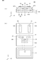
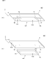
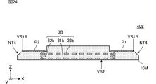
図1(A)は第1の実施形態に係る電子部品101の断面図であり、図1(B)は電子部品101の分解斜視図である。図2(A)は電極非形成部PEを示す、電子部品101の平面図であり、図2(B)は図1(A)におけるDP1部の拡大図である。なお、図1(A)において、各部の厚みは誇張して図示している。以降の各実施形態における断面図についても同様である。図2(A)では、構造を解りやすくするため、電極非形成部PEをハッチングで示している。 << First Embodiment >>
FIG. 1A is a cross-sectional view of theelectronic component 101 according to the first embodiment, and FIG. 1B is an exploded perspective view of the electronic component 101. FIG. 2A is a plan view of the electronic component 101 showing the electrode non-forming portion PE, and FIG. 2B is an enlarged view of the DP1 portion in FIG. Note that in FIG. 1A, the thickness of each portion is exaggerated. The same applies to the sectional views in the following embodiments. In FIG. 2A, in order to make the structure easy to understand, the electrode non-forming portion PE is indicated by hatching.
図1(A)は第1の実施形態に係る電子部品101の断面図であり、図1(B)は電子部品101の分解斜視図である。図2(A)は電極非形成部PEを示す、電子部品101の平面図であり、図2(B)は図1(A)におけるDP1部の拡大図である。なお、図1(A)において、各部の厚みは誇張して図示している。以降の各実施形態における断面図についても同様である。図2(A)では、構造を解りやすくするため、電極非形成部PEをハッチングで示している。 << First Embodiment >>
FIG. 1A is a cross-sectional view of the
本発明における「電子部品」は、導電性接合材および絶縁性接合材を用いて実装基板等に実装される素子である。また、本発明における「電子機器」は、上記電子部品および実装基板等を備える装置であり、例えば携帯電話端末、いわゆるスマートフォン、タブレット端末、ノートPCやPDA、ウェアラブル端末(いわゆるスマートウォッチやスマートグラス等)、カメラ、ゲーム機、玩具等である。
The “electronic component” in the present invention is an element mounted on a mounting board or the like using a conductive bonding material and an insulating bonding material. In addition, the “electronic device” in the present invention is a device including the above-described electronic components, a mounting substrate, and the like. ), Cameras, game machines, toys and the like.
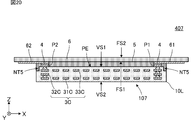
電子部品101は、第1主面VS1および第2主面VS2を有する絶縁基材10と、絶縁基材10に形成されるコイル3(後に詳述する。)と、第1主面VS1に形成される実装電極P1,P2と、を備える。本実施形態では、絶縁基材10の第1主面VS1が「実装面」に相当し、第1主面VS1に対向する第2主面VS2が「天面」に相当する。
The electronic component 101 is formed on the insulating base material 10 having the first main surface VS1 and the second main surface VS2, the coil 3 (described in detail later) formed on the insulating base material 10, and the first main surface VS1. Mounting electrodes P1 and P2. In the present embodiment, the first main surface VS1 of the insulating base material 10 corresponds to a “mounting surface”, and the second main surface VS2 facing the first main surface VS1 corresponds to a “top surface”.
絶縁基材10は、長手方向がX軸方向に一致する熱可塑性樹脂の略直方体である。絶縁基材10は、第1主面VS1の外縁部の全周に亘って形成される切り欠き部NT1を有する。図2(B)等に示すように、切り欠き部NT1の断面形状はL字形である。また、電子部品101は、図2(A)に示すように、電極非形成部PEを有する。電極非形成部PEは、第1主面VS1のうち実装電極P1,P2が形成されていない部分である。
The insulating base material 10 is a substantially rectangular parallelepiped of a thermoplastic resin whose longitudinal direction coincides with the X-axis direction. Insulating base material 10 has notch part NT1 formed over the perimeter of the outer edge part of the 1st principal surface VS1. As shown in FIG. 2B and the like, the cross-sectional shape of the notch NT1 is L-shaped. Moreover, the electronic component 101 has the electrode non-formation part PE as shown to FIG. 2 (A). The electrode non-forming portion PE is a portion where the mounting electrodes P1 and P2 are not formed in the first main surface VS1.
絶縁基材10は、図1(B)に示すように、熱可塑性樹脂からなる複数の絶縁基材層11,12,13の順に積層して形成される。複数の絶縁基材層11,12,13は、それぞれ平面形状が矩形の平板であり、長手方向がX軸方向に一致する。複数の絶縁基材層11,12,13は、例えば液晶ポリマー(LCP)を主材料とするシートである。
As shown in FIG. 1B, the insulating base material 10 is formed by laminating a plurality of insulating base material layers 11, 12, 13 made of thermoplastic resin in this order. Each of the plurality of insulating base layers 11, 12, and 13 is a flat plate having a rectangular planar shape, and the longitudinal direction coincides with the X-axis direction. The plurality of insulating base layers 11, 12, and 13 are sheets mainly made of a liquid crystal polymer (LCP), for example.
絶縁基材層11の表面には、導体21が形成されている。導体21は、絶縁基材層11の第1角(図1(B)における絶縁基材層11の左下角)付近に配置され、X軸方向およびY軸方向に延伸するL字形の導体である。導体21は、例えばCu箔等による導体パターンである。
The conductor 21 is formed on the surface of the insulating base layer 11. The conductor 21 is an L-shaped conductor that is disposed near the first corner of the insulating base layer 11 (the lower left corner of the insulating base layer 11 in FIG. 1B) and extends in the X-axis direction and the Y-axis direction. . The conductor 21 is a conductor pattern made of, for example, Cu foil.
絶縁基材層12の表面には、コイル導体31および導体22が形成されている。コイル導体31は、絶縁基材層12の外形に沿って巻回される約2ターン強の矩形スパイラル状の導体である。導体22は、絶縁基材層12の第1角(図1(B)における絶縁基材層12の左下角)付近に配置される矩形の導体である。コイル導体31および導体22は、例えばCu箔等による導体パターンである。
The coil conductor 31 and the conductor 22 are formed on the surface of the insulating base layer 12. The coil conductor 31 is a rectangular spiral conductor having a little over two turns that is wound along the outer shape of the insulating base layer 12. The conductor 22 is a rectangular conductor disposed near the first corner of the insulating base layer 12 (the lower left corner of the insulating base layer 12 in FIG. 1B). The coil conductor 31 and the conductor 22 are conductor patterns made of, for example, Cu foil.
絶縁基材層13の表面には、2つの実装電極P1,P2が形成されている。実装電極P1,P2は、長手方向がY軸方向に一致する矩形の導体である。本実施形態に係る実装電極P1,P2は、絶縁基材層13の第1辺(図1(B)における絶縁基材層13の右辺)付近および第2辺(絶縁基材層13の左辺)付近にそれぞれ配置され、X軸方向に沿って配列されている。実装電極P1,P2は、例えばCu箔等による導体パターンである。
Two mounting electrodes P1 and P2 are formed on the surface of the insulating base layer 13. The mounting electrodes P1 and P2 are rectangular conductors whose longitudinal direction coincides with the Y-axis direction. The mounting electrodes P1 and P2 according to the present embodiment are near the first side (the right side of the insulating base layer 13 in FIG. 1B) and the second side (the left side of the insulating base layer 13) of the insulating base layer 13. They are arranged in the vicinity and arranged along the X-axis direction. The mounting electrodes P1 and P2 are conductor patterns made of, for example, Cu foil.
図1(B)に示すように、実装電極P1は、絶縁基材層13に形成される層間接続導体V33を介して、コイル導体31の第1端に接続される。コイル導体31の第2端は、絶縁基材層12に形成される層間接続導体V32を介して、導体21の第1端に接続される。導体21の第2端は、絶縁基材層12,13に形成される導体22および層間接続導体V21,V22を介して、実装電極P2に接続される。
As shown in FIG. 1B, the mounting electrode P1 is connected to the first end of the coil conductor 31 through an interlayer connection conductor V33 formed on the insulating base layer 13. The second end of the coil conductor 31 is connected to the first end of the conductor 21 via an interlayer connection conductor V32 formed in the insulating base layer 12. The second end of the conductor 21 is connected to the mounting electrode P2 via the conductor 22 formed on the insulating base material layers 12 and 13 and the interlayer connection conductors V21 and V22.
このように、電子部品101では、絶縁基材層12に形成されるコイル導体31を含んで約2ターン強の矩形スパイラル状のコイル3が構成される。図1(A)に示すように、コイル3は絶縁基材10の内部に形成され、コイル3の両端はそれぞれ実装電極P1,P2に接続される。また、コイル3は、図1(A)に示すように、複数の絶縁基材層11,12,13の積層方向(Z軸方向)に巻回軸AXを有する。
As described above, in the electronic component 101, the rectangular spiral coil 3 having about two turns is configured including the coil conductor 31 formed on the insulating base layer 12. As shown in FIG. 1 (A), the coil 3 is formed inside an insulating substrate 10, and both ends of the coil 3 are connected to mounting electrodes P1 and P2, respectively. Further, the coil 3 has a winding axis AX in the stacking direction (Z-axis direction) of the plurality of insulating base material layers 11, 12, 13 as shown in FIG.
なお、本実施形態では、複数の絶縁基材層11,12,13の積層方向(Z軸方向)に巻回軸AXを有するコイル3の例を示したが、コイル3の巻回軸AXとZ軸方向とが厳密に一致することに限るものではない。本発明において「複数の絶縁基材層の積層方向に巻回軸を有する」とは、例えばコイル3の巻回軸AXがZ軸方向に対して-30°から+30°の範囲内である場合も含む。
In the present embodiment, the example of the coil 3 having the winding axis AX in the stacking direction (Z-axis direction) of the plurality of insulating base layers 11, 12, and 13 has been shown. It is not limited to exactly matching the Z-axis direction. In the present invention, “having a winding axis in the stacking direction of the plurality of insulating base layers” means, for example, when the winding axis AX of the coil 3 is within a range of −30 ° to + 30 ° with respect to the Z-axis direction. Including.
また、電子部品101では、図1(A)等に示すように、第1主面VS1の面積が、第1主面VS1に平行な断面(XY平面に平行な断面)のうち、第1主面VS1の面積とは異なり、且つ、第1主面に最も近い断面(例えば、絶縁基材層12と絶縁基材層13との界面)の面積よりも小さい。
In the electronic component 101, as shown in FIG. 1A and the like, the area of the first main surface VS1 is the first main surface among the cross sections parallel to the first main surface VS1 (the cross sections parallel to the XY plane). Unlike the area of the surface VS1, it is smaller than the area of the cross section closest to the first main surface (for example, the interface between the insulating base material layer 12 and the insulating base material layer 13).
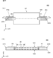
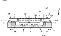
次に、導電性接合材および絶縁性接合材を用いて、電子部品101を実装基板に実装した状態について、図を参照して説明する。図3は、第1の実施形態に係る電子機器301の主要部を示す断面図である。
Next, a state where the electronic component 101 is mounted on the mounting substrate using the conductive bonding material and the insulating bonding material will be described with reference to the drawings. FIG. 3 is a cross-sectional view illustrating a main part of the electronic device 301 according to the first embodiment.
電子機器301は、電子部品101および実装基板201等を備える。実装基板201は例えばプリント配線基板である。
The electronic device 301 includes an electronic component 101, a mounting substrate 201, and the like. The mounting board 201 is, for example, a printed wiring board.
実装基板201の主面には導体51,52が形成されている。導体51,52は、導電性接合材4を介して実装電極P1,P2にそれぞれ接続される。図2(A)に示す電極非形成部PEおよび切り欠き部NT1は、絶縁性接合材5を介して実装基板201に接合される。導電性接合材4は例えばはんだ等であり、絶縁性接合材5は、導電性接合材4の溶融温度と同程度の温度で熱硬化する接着剤であり、例えばエポキシ系熱硬化性樹脂の接着剤である。なお、絶縁性接合材は例えばアンダーフィル等であってもよい。
Conductors 51 and 52 are formed on the main surface of the mounting substrate 201. The conductors 51 and 52 are connected to the mounting electrodes P1 and P2 through the conductive bonding material 4, respectively. The electrode non-forming part PE and the notch part NT1 shown in FIG. 2A are bonded to the mounting substrate 201 via the insulating bonding material 5. The conductive bonding material 4 is, for example, solder or the like, and the insulating bonding material 5 is an adhesive that is thermally cured at a temperature approximately equal to the melting temperature of the conductive bonding material 4, for example, adhesion of an epoxy thermosetting resin. It is an agent. The insulating bonding material may be an underfill, for example.
本実施形態に係る電子部品101は、例えば次の工程で実装基板201に実装される。
The electronic component 101 according to the present embodiment is mounted on the mounting substrate 201 in the following process, for example.
まず、導体51,52にペースト状の導電性接合材4を印刷して、実装基板201上に熱硬化前の絶縁性接合材5を塗布した後、実装電極P1,P2がそれぞれ導体51,52上に配置されるよう電子部品101をマウンター等でマウントする。その後、リフロープロセスにより、実装電極P1,P2は導電性接合材4を介して導体51,52にそれぞれ接合され、電極非形成部PEおよび切り欠き部NT1は絶縁性接合材5を介して実装基板201に接合される。このリフロープロセス時の温度によって、ペースト状の導電性接合材4は溶融し、実装電極P1,P2が導体51,52にそれぞれ接続される。同時に、熱硬化前の絶縁性接合材5は熱硬化し、電極非形成部PEおよび切り欠き部NT1が実装基板201に接合される。
First, after the paste-like conductive bonding material 4 is printed on the conductors 51 and 52 and the insulating bonding material 5 before thermosetting is applied on the mounting substrate 201, the mounting electrodes P1 and P2 are respectively connected to the conductors 51 and 52. The electronic component 101 is mounted with a mounter or the like so as to be arranged above. Thereafter, the mounting electrodes P1 and P2 are bonded to the conductors 51 and 52 via the conductive bonding material 4 by the reflow process, respectively, and the electrode non-forming portion PE and the notch portion NT1 are mounted via the insulating bonding material 5 to the mounting substrate. It is joined to 201. Due to the temperature during the reflow process, the paste-like conductive bonding material 4 is melted, and the mounting electrodes P1 and P2 are connected to the conductors 51 and 52, respectively. At the same time, the insulating bonding material 5 before thermosetting is thermoset, and the electrode non-forming portion PE and the notch NT1 are bonded to the mounting substrate 201.
次に、比較例として、切り欠き部を備えていない電子部品を実装基板に実装した電子機器について説明する。図4は、比較例である電子機器300の主要部を示す断面図である。
Next, as a comparative example, an electronic device in which an electronic component not provided with a notch is mounted on a mounting board will be described. FIG. 4 is a cross-sectional view illustrating a main part of an electronic device 300 as a comparative example.
電子機器300は、電子部品100および実装基板201等を備える。電子部品100は、切り欠き部を備えていない点で電子部品101と異なり、その他の構成は電子部品101と同じである。電子部品100は、電極非形成部PE0のみが絶縁性接合材5を介して実装基板201に接合される。図3および図4に示すように、絶縁性接合材5を含めた電子部品100の実装面積は、絶縁性接合材5を含めた電子部品101の実装面積と略同じ大きさである。
The electronic device 300 includes an electronic component 100, a mounting board 201, and the like. The electronic component 100 is different from the electronic component 101 in that it does not include a notch, and the other configuration is the same as the electronic component 101. In the electronic component 100, only the electrode non-forming part PE0 is bonded to the mounting substrate 201 via the insulating bonding material 5. As shown in FIGS. 3 and 4, the mounting area of the electronic component 100 including the insulating bonding material 5 is substantially the same as the mounting area of the electronic component 101 including the insulating bonding material 5.
一方、電子部品101では、図3に示すように、電極非形成部PEおよび切り欠き部NT1が、絶縁性接合材5を介して実装基板201に接合される。そのため、図4に示す電極非形成部PE0のみが絶縁性接合材5を介して実装基板201に接合される場合に比べて、絶縁性接合材5に接する面積は大きくなり、電子部品(絶縁基材)と絶縁性接合材5との間の接合強度は高まる。
On the other hand, in the electronic component 101, as shown in FIG. 3, the electrode non-forming part PE and the notch part NT1 are bonded to the mounting substrate 201 via the insulating bonding material 5. Therefore, compared with the case where only the electrode non-forming portion PE0 shown in FIG. 4 is bonded to the mounting substrate 201 via the insulating bonding material 5, the area in contact with the insulating bonding material 5 is increased, and the electronic component (insulating base) Material) and the insulating bonding material 5 are increased in bonding strength.
本実施形態によれば、次のような効果を奏する。
According to this embodiment, the following effects can be obtained.
(a)本実施形態に係る電子部品101は、第1主面VS1の面積が、第1主面VS1に平行な断面(XY平面に平行な断面)のうち、第1主面VS1の面積とは異なり、且つ、第1主面VS1に最も近い断面の面積よりも小さい。また、電子部品101は、第1主面VS1の外縁部に形成される切り欠き部NT1を備え、この切り欠き部NT1および電極非形成部PEが、絶縁性接合材5を介して実装基板201に接合される。この構成により、絶縁性接合材5を含めた電子部品の実装面積を大きくすることなく、電子部品101(絶縁基材10)と絶縁性接合材5との間の接合強度は高めることができ、実装基板等に対する接合信頼性を高めた電子部品を実現できる。また、この電子部品が実装された実装基板を備える電子機器を実現できる。
(A) In the electronic component 101 according to the present embodiment, the area of the first main surface VS1 is the same as the area of the first main surface VS1 in the cross section parallel to the first main surface VS1 (the cross section parallel to the XY plane). And is smaller than the area of the cross section closest to the first main surface VS1. In addition, the electronic component 101 includes a cutout portion NT1 formed at the outer edge portion of the first main surface VS1. The cutout portion NT1 and the electrode non-formed portion PE are mounted on the mounting substrate 201 via the insulating bonding material 5. To be joined. With this configuration, the bonding strength between the electronic component 101 (insulating base material 10) and the insulating bonding material 5 can be increased without increasing the mounting area of the electronic component including the insulating bonding material 5, An electronic component with improved bonding reliability to a mounting substrate or the like can be realized. In addition, an electronic device including a mounting substrate on which the electronic component is mounted can be realized.
(b)本実施形態では、絶縁性接合材5が導電性接合材4の溶融温度と同程度の温度で熱硬化する接着剤である。この構成により、導電性接合材4を介して実装電極P1,P2を導体51,52にそれぞれ接続する工程と、絶縁性接合材5を介して切り欠き部NT1および電極非形成部PEを実装基板201に接合する工程と、を同時に行うことができる。したがって、実装基板に電子部品を実装する工程が簡素化できる。
(B) In this embodiment, the insulating bonding material 5 is an adhesive that is thermoset at a temperature similar to the melting temperature of the conductive bonding material 4. With this configuration, the step of connecting the mounting electrodes P1 and P2 to the conductors 51 and 52 via the conductive bonding material 4 and the notch portion NT1 and the electrode non-forming portion PE via the insulating bonding material 5 are mounted on the mounting board. The step of bonding to 201 can be performed at the same time. Therefore, the process of mounting electronic components on the mounting board can be simplified.
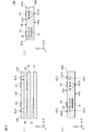
本実施形態に係る電子部品101は、例えば次の工程で製造される。図5は、電子部品101の製造工程を順に示す断面図である。
The electronic component 101 according to the present embodiment is manufactured by, for example, the following process. FIG. 5 is a cross-sectional view sequentially illustrating the manufacturing process of the electronic component 101.
まず、図5中の(1)に示すように、集合基板状態の絶縁基材層11に、導体21を形成する。具体的には、絶縁基材層11の片側主面に金属箔(例えばCu箔)をラミネートし、その金属箔をフォトリソグラフィでパターンニングすることで、導体21を形成する。絶縁基材層11は例えば液晶ポリマー等の熱可塑性樹脂シートである。
First, as shown in (1) in FIG. 5, the conductor 21 is formed on the insulating base material layer 11 in the aggregate substrate state. Specifically, a conductor 21 is formed by laminating a metal foil (for example, Cu foil) on one main surface of the insulating base material layer 11 and patterning the metal foil by photolithography. The insulating base material layer 11 is a thermoplastic resin sheet such as a liquid crystal polymer.
次に、集合基板状態の絶縁基材層12に、コイル導体31および導体22を形成する。具体的には、絶縁基材層12の片側主面に金属箔(例えばCu箔)をラミネートし、その金属箔をフォトリソグラフィでパターンニングすることで、コイル導体31および導体22を形成する。絶縁基材層12は例えば液晶ポリマー等の熱可塑性樹脂シートである。
Next, the coil conductor 31 and the conductor 22 are formed on the insulating base material layer 12 in the aggregate substrate state. Specifically, the coil conductor 31 and the conductor 22 are formed by laminating a metal foil (for example, Cu foil) on one main surface of the insulating base material layer 12 and patterning the metal foil by photolithography. The insulating base layer 12 is a thermoplastic resin sheet such as a liquid crystal polymer.
絶縁基材層(複数の絶縁基材層のうち1つ以上の絶縁基材層)に、コイル導体を形成するこの工程が、本発明における「導体形成工程」の一例である。
This step of forming a coil conductor on an insulating base layer (one or more insulating base layers among a plurality of insulating base layers) is an example of the “conductor forming step” in the present invention.
また、集合基板状態の絶縁基材層13の表面(絶縁基材10を形成した後に第1主面VS1になる絶縁基材層の表面)に、実装電極P1,P2を形成する。具体的には、集合基板状態の絶縁基材層13の片側主面に金属箔(例えばCu箔)をラミネートし、その金属箔をフォトリソグラフィでパターンニングすることで、実装電極P1,P2を形成する。これにより、絶縁基材10を形成した後に第1主面VS1になる絶縁基材層の表面のうち、実装電極P1,P2が形成されない電極費形成領域(PE)が形成される。上述したように、電極非形成部(PE)は、実装基板に電子部品を実装した状態で、絶縁性接合材が接する部分である。絶縁基材層13は例えば液晶ポリマー等の熱可塑性樹脂シートである。
Further, the mounting electrodes P1 and P2 are formed on the surface of the insulating base material layer 13 in the aggregate substrate state (the surface of the insulating base material layer that becomes the first main surface VS1 after forming the insulating base material 10). Specifically, the mounting electrodes P1 and P2 are formed by laminating a metal foil (for example, Cu foil) on one side main surface of the insulating base material layer 13 in the aggregate substrate state and patterning the metal foil by photolithography. To do. Thereby, the electrode expense formation area (PE) in which the mounting electrodes P1 and P2 are not formed is formed in the surface of the insulating base material layer that becomes the first main surface VS1 after the insulating base material 10 is formed. As described above, the electrode non-forming portion (PE) is a portion where the insulating bonding material is in contact with the electronic component mounted on the mounting substrate. The insulating base layer 13 is a thermoplastic resin sheet such as a liquid crystal polymer.
絶縁基材の第1主面になる絶縁基材層の表面に、実装電極を形成する(同時に、絶縁基材の第1主面になる絶縁基材層の表面のうち、実装電極が形成されない電極非形成部PEを形成する)この工程が、本発明における「電極形成工程」の一例である。
A mounting electrode is formed on the surface of the insulating base material layer that becomes the first main surface of the insulating base material (at the same time, no mounting electrode is formed among the surfaces of the insulating base material layer that becomes the first main surface of the insulating base material). This step (forming the electrode non-forming portion PE) is an example of the “electrode forming step” in the present invention.
なお、複数の絶縁基材層11,12,13には、他に層間接続導体(図1(B)における層間接続導体V22,V23,V32,V33)が形成される。層間接続導体は、レーザー等で貫通孔を設けた後、Cu,Ag,Sn,Ni,Mo等のうち1以上もしくはそれらの合金を含む導電性ペーストを配設し、後の加熱加圧(本発明の「基材形成工程」)で硬化させることによって設けられる。そのため、層間接続導体は、後の加熱加圧時の温度よりも融点が低い材料とする。
In addition, interlayer connection conductors (interlayer connection conductors V22, V23, V32, and V33 in FIG. 1B) are formed on the plurality of insulating base material layers 11, 12, and 13 in addition. The interlayer connection conductor is provided with a conductive paste containing one or more of Cu, Ag, Sn, Ni, Mo or the like or an alloy thereof after providing a through hole with a laser or the like, It is provided by curing in the “base material forming step”) of the invention. Therefore, the interlayer connection conductor is made of a material having a melting point lower than the temperature at the time of subsequent heating and pressurization.
次に、絶縁基材層11,12,13の順に積層し、積層した複数の絶縁基材層11,12,13を加熱加圧(一括プレス)することにより、絶縁基材10Bを形成する。
Next, the insulating base material layers 11, 12, and 13 are laminated in this order, and the insulating base material 10 </ b> B is formed by heating and pressing (collective pressing) the plurality of laminated insulating base material layers 11, 12, and 13.
「導体形成工程」の後に、積層した複数の絶縁基材層を加熱加圧することにより、絶縁基材を形成するこの工程が、本発明における「基材形成工程」の一例である。
This step of forming an insulating base material by heating and pressing a plurality of laminated insulating base material layers after the “conductor forming step” is an example of the “base material forming step” in the present invention.
上記工程の後、図5中の(2)に示す分離線DLに沿って、集合基板状態の絶縁基材10Bを個々の個片(絶縁基材10A)に分離する。
After the above process, the insulating base material 10B in the aggregated substrate state is separated into individual pieces (insulating base material 10A) along the separation line DL shown in (2) in FIG.
次に、図5中の(3)に示すように、絶縁基材10Aの第1主面VS1の外縁部E1近傍をレーザーで研削することにより、切り欠き部NT1を形成する。具体的には、第1主面VS1の外縁部E1近傍を全周に亘ってレーザーで研削することで、切り欠き部NT1を形成する。これにより、図5中の(4)に示す電子部品101を得る。
Next, as shown in (3) in FIG. 5, the notch NT1 is formed by grinding the vicinity of the outer edge E1 of the first main surface VS1 of the insulating base 10A with a laser. Specifically, the notch NT1 is formed by grinding the vicinity of the outer edge E1 of the first main surface VS1 with a laser over the entire circumference. Thereby, the electronic component 101 shown in (4) in FIG. 5 is obtained.
上記製造方法により、導電性接合材および絶縁性接合材を用いて実装基板に実装する場合において、絶縁性接合材を含めた電子部品の実装面積を大きくすることなく、実装基板に対する接合信頼性を高めた電子部品を容易に製造できる。
When mounting on a mounting board using a conductive bonding material and an insulating bonding material by the above manufacturing method, the bonding reliability to the mounting board is increased without increasing the mounting area of the electronic component including the insulating bonding material. Elevated electronic components can be easily manufactured.
また、本実施形態では、絶縁基材層が熱可塑性樹脂からなる。上記製造方法によれば、積層した複数の絶縁基材層11,12,13を一括プレスすることにより、絶縁基材10Aを容易に形成できるため、絶縁基材の製造工程の工数が削減され、コストを低く抑えることができる。
In this embodiment, the insulating base layer is made of a thermoplastic resin. According to the above manufacturing method, since the insulating base material 10A can be easily formed by collectively pressing the laminated insulating base material layers 11, 12, and 13, the man-hours for the manufacturing process of the insulating base material are reduced, Cost can be kept low.
なお、本実施形態では、「基材形成工程」の前に、「電極形成工程」が行われる例を示したが、この構成に限定されるものではない。「電極形成工程」は、「基材形成工程」の後に行われてもよい。すなわち、本発明における「電極形成工程」は、「基材形成工程」の後で、絶縁基材10の第1主面VS1に、実装電極P1,P2を形成してもよい。
In the present embodiment, an example in which the “electrode forming step” is performed before the “base material forming step” is shown, but the present invention is not limited to this configuration. The “electrode forming step” may be performed after the “base material forming step”. That is, in the “electrode forming step” in the present invention, the mounting electrodes P1 and P2 may be formed on the first main surface VS1 of the insulating base material 10 after the “base material forming step”.
《第2の実施形態》
第2の実施形態では、絶縁基材の形状が第1の実施形態とは異なる例について示す。 << Second Embodiment >>
In 2nd Embodiment, it shows about the example from which the shape of an insulation base material differs from 1st Embodiment.
第2の実施形態では、絶縁基材の形状が第1の実施形態とは異なる例について示す。 << Second Embodiment >>
In 2nd Embodiment, it shows about the example from which the shape of an insulation base material differs from 1st Embodiment.
図6(A)は第2の実施形態に係る電子部品102の断面図であり、図6(B)は図6(A)におけるDP2部の拡大図である。
6A is a cross-sectional view of the electronic component 102 according to the second embodiment, and FIG. 6B is an enlarged view of the DP2 portion in FIG. 6A.
電子部品102は、絶縁基材の形状が第1の実施形態に係る電子部品101と異なる。その他の構成については、電子部品101と実質的に同じである。
The electronic component 102 is different from the electronic component 101 according to the first embodiment in the shape of the insulating base material. Other configurations are substantially the same as those of the electronic component 101.
電子部品102は、第1主面VS1、端面SSおよび第2主面VS2を有する絶縁基材10Cと、絶縁基材10Cに形成されるコイル3と、第1主面VS1に形成される実装電極P1,P2と、凹凸部RPと、を備える。端面SSは、第1主面VS1に接続される面である。
The electronic component 102 includes an insulating base material 10C having a first main surface VS1, an end surface SS, and a second main surface VS2, a coil 3 formed on the insulating base material 10C, and a mounting electrode formed on the first main surface VS1. P1 and P2 and the uneven | corrugated | grooved part RP are provided. The end surface SS is a surface connected to the first main surface VS1.
絶縁基材10Cは、第1主面VS1の面積が第2主面VS2の面積よりも小さな熱可塑性樹脂の台形柱である。言い換えると、絶縁基材10Cは、第2主面VS2から第1主面VS1(+Z方向)に向かってテーパー状に形成されている。そのため、電子部品102では、第1主面VS1の面積が、第1主面VS1に平行な断面(XY平面の断面)のうち、第1主面VS1の面積とは異なり、且つ、第1主面VS1に最も近い断面(例えば、図6(A)に示す絶縁基材10Cのうち、第1主面VS1よりも-Z方向におけるXY平面に平行な断面)よりも小さい。
The insulating base material 10C is a trapezoidal column made of a thermoplastic resin in which the area of the first main surface VS1 is smaller than the area of the second main surface VS2. In other words, the insulating base material 10C is formed in a tapered shape from the second main surface VS2 toward the first main surface VS1 (+ Z direction). Therefore, in the electronic component 102, the area of the first main surface VS1 is different from the area of the first main surface VS1 in the cross section (cross section of the XY plane) parallel to the first main surface VS1, and the first main surface VS1. It is smaller than the cross section closest to the surface VS1 (for example, in the insulating base material 10C shown in FIG. 6A, the cross section parallel to the XY plane in the −Z direction than the first main surface VS1).
また、電子部品102の電極非形成部PE(第1主面VS1のうち実装電極P1,P2が形成されていない部分)には、凹凸部RPが形成されている。凹凸部RPは、レーザーの照射等により電極非形成部PEに形成される溝である。
Further, an uneven portion RP is formed in the electrode non-forming portion PE of the electronic component 102 (the portion of the first main surface VS1 where the mounting electrodes P1 and P2 are not formed). The uneven part RP is a groove formed in the electrode non-forming part PE by laser irradiation or the like.
次に、導電性接合材および絶縁性接合材を用いて、電子部品102を実装基板に実装した状態について、図を参照して説明する。図7は、第2の実施形態に係る電子機器302の主要部を示す断面図である。
Next, a state where the electronic component 102 is mounted on the mounting substrate using the conductive bonding material and the insulating bonding material will be described with reference to the drawings. FIG. 7 is a cross-sectional view illustrating a main part of the electronic device 302 according to the second embodiment.
電子機器302は、電子部品102および実装基板201等を備える。実装基板201は、第1の実施形態で説明したものと同じである。
The electronic device 302 includes an electronic component 102, a mounting substrate 201, and the like. The mounting substrate 201 is the same as that described in the first embodiment.
導体51,52は、導電性接合材4を介して実装電極P1,P2にそれぞれ接続される。端面SSの一部および電極非形成部PEは、絶縁性接合材5を介して実装基板201に接合される。
The conductors 51 and 52 are connected to the mounting electrodes P1 and P2 through the conductive bonding material 4, respectively. Part of the end surface SS and the electrode non-forming portion PE are bonded to the mounting substrate 201 via the insulating bonding material 5.
本実施形態に係る電子部品102によれば、第1の実施形態で述べた効果以外に、次のような効果を奏する。
The electronic component 102 according to the present embodiment has the following effects in addition to the effects described in the first embodiment.
(c)本実施形態では、電極非形成部PEに形成される凹凸部RPを備える。この構成では、電極非形成部PEに凹凸部RPが形成されていない場合に比べて、実装基板201への実装状態で絶縁性接合材5に接する電極非形成部PEの表面積が大きくなるため、絶縁基材10Cと絶縁性接合材5との間の接合強度はさらに高まる。
(C) In this embodiment, the uneven | corrugated | grooved part RP formed in the electrode non-formation part PE is provided. In this configuration, since the surface area of the electrode non-forming part PE in contact with the insulating bonding material 5 in the mounting state on the mounting substrate 201 is larger than when the uneven part RP is not formed in the electrode non-forming part PE, The bonding strength between the insulating base material 10C and the insulating bonding material 5 is further increased.
本実施形態で示したように、絶縁基材の形状は、第1主面VS1の面積が第2主面VS2の面積よりも小さな台形柱であってもよい。なお、本発明における絶縁基材の形状は、第1主面VS1の面積が、第1主面VS1に平行な断面のうち、第1主面VS1の面積とは異なり、且つ、第1主面VS1に最も近い断面の面積よりも小さい構成を満たせば、適宜変更可能である。
As shown in this embodiment, the shape of the insulating base material may be a trapezoidal column in which the area of the first main surface VS1 is smaller than the area of the second main surface VS2. The shape of the insulating base material in the present invention is such that the area of the first main surface VS1 is different from the area of the first main surface VS1 in the cross section parallel to the first main surface VS1, and the first main surface If the configuration smaller than the area of the cross section closest to VS1 is satisfied, it can be changed as appropriate.
本実施形態に係る電子部品102は、例えば次の工程で製造される。図8は、電子部品102の製造工程を順に示す断面図である。なお、図5を用いて説明した製造工程と同一のものについては、具体的な製造工程の説明は省略する。
The electronic component 102 according to the present embodiment is manufactured by, for example, the following process. FIG. 8 is a cross-sectional view sequentially illustrating the manufacturing process of the electronic component 102. In addition, about the same thing as the manufacturing process demonstrated using FIG. 5, description of a specific manufacturing process is abbreviate | omitted.
まず、図8中の(1)に示すように、絶縁基材層11に導体21を形成し、絶縁基材層12にコイル導体31および導体22を形成し、絶縁基材層13に実装電極P1,P2を形成する(「導体形成工程」および「電極形成工程」)。
First, as shown in (1) in FIG. 8, the conductor 21 is formed on the insulating base layer 11, the coil conductor 31 and the conductor 22 are formed on the insulating base layer 12, and the mounting electrode is formed on the insulating base layer 13. P1 and P2 are formed ("conductor formation process" and "electrode formation process").
次に、絶縁基材層11,12,13の順に積層し、積層した複数の絶縁基材層11,12,13を加熱加圧することにより、絶縁基材10Bを形成する(「基材形成工程」)。
Next, the insulating base material layers 11, 12, and 13 are laminated in this order, and the insulating base material layers 10 B are formed by heating and pressurizing the plurality of laminated insulating base material layers 11, 12, and 13 (“base material forming step”). ").
次に、図8中の(2)に示すように、分離線DLに沿って、集合基板状態の絶縁基材10Bの第1主面VS1側からレーザーLRで研削することにより個片(絶縁基材10D)に分離する。この工程により、絶縁基材10Dは、図8中の(3)に示すように、第2主面VS2から第1主面VS1(+Z方向)に向かってテーパー状に形成される。
Next, as shown in (2) in FIG. 8, individual pieces (insulating bases) are ground by laser LR along the separating line DL from the first main surface VS1 side of the insulating base material 10B in the aggregated substrate state. Material 10D). By this step, the insulating base 10D is formed in a tapered shape from the second main surface VS2 toward the first main surface VS1 (+ Z direction) as shown in (3) in FIG.
「基材形成工程」の後に、絶縁基材を第1主面側からレーザーで研削することにより個片に分離するこの工程が、本発明における「分離工程」の一例である。
This step of separating the insulating base material into individual pieces by grinding with a laser from the first main surface side after the “base material forming step” is an example of the “separation step” in the present invention.
次に、図8中の(3)に示すように、電極非形成部PEに凹凸部RPを形成する。凹凸部RPは、例えば電極非形成部PEに第1主面VS1側からレーザーを照射することにより形成される。レーザーによって形成される穴は、レーザーの照射面から反対面に向かってその面積が小さくなる。そのため、これを利用することで、単にレーザーを照射するだけでテーパーが形成できる。
Next, as shown in (3) in FIG. 8, the uneven portion RP is formed in the electrode non-forming portion PE. The uneven part RP is formed by, for example, irradiating the electrode non-forming part PE with a laser from the first main surface VS1 side. The area of the hole formed by the laser decreases from the laser irradiation surface toward the opposite surface. Therefore, by using this, a taper can be formed simply by irradiating a laser.
《第3の実施形態》
第3の実施形態では、コイルの形状が、第1・第2の実施形態とは異なる例について示す。 << Third Embodiment >>
In the third embodiment, an example in which the shape of the coil is different from those in the first and second embodiments will be described.
第3の実施形態では、コイルの形状が、第1・第2の実施形態とは異なる例について示す。 << Third Embodiment >>
In the third embodiment, an example in which the shape of the coil is different from those in the first and second embodiments will be described.
図9(A)は第3の実施形態に係る電子部品103の断面図であり、図9(B)は電子部品103の分解平面図である。
FIG. 9A is a cross-sectional view of the electronic component 103 according to the third embodiment, and FIG. 9B is an exploded plan view of the electronic component 103.
電子部品103は、コイルの形状が第1の実施形態に係る電子部品101と異なる。また、電子部品103は、切り欠き部の形状が電子部品101と異なる。その他の構成については、電子部品101と実質的に同じである。
The electronic component 103 is different from the electronic component 101 according to the first embodiment in the shape of the coil. The electronic component 103 is different from the electronic component 101 in the shape of the notch. Other configurations are substantially the same as those of the electronic component 101.
電子部品103は、第1主面VS1および第2主面VS2を有する絶縁基材10Eと、絶縁基材10Eに形成されるコイル3A(後に詳述する。)と、実装電極P1,P2と、を備える。
The electronic component 103 includes an insulating base material 10E having a first main surface VS1 and a second main surface VS2, a coil 3A (described in detail later) formed on the insulating base material 10E, mounting electrodes P1 and P2, Is provided.
絶縁基材10Eは、図9(A)および図9(B)に示すように、第1主面VS1の外縁部に形成される切り欠き部NT2を有する。切り欠き部NT2は、第1主面VS1の第1辺(図9(B)における絶縁基材層13の右辺)および第2辺(図9(B)における絶縁基材層13の左辺)近傍に形成されている。切り欠き部NT2の断面形状はC字形である。
As shown in FIGS. 9A and 9B, the insulating base material 10E has a notch NT2 formed at the outer edge of the first main surface VS1. Cutout portion NT2 is in the vicinity of the first side (the right side of insulating base layer 13 in FIG. 9B) and the second side (the left side of insulating base layer 13 in FIG. 9B) of first main surface VS1. Is formed. The cross-sectional shape of the notch NT2 is C-shaped.
絶縁基材10Eは、図9(B)に示すように、熱可塑性樹脂からなる複数の絶縁基材層11,12,13の順に積層して形成される。
As shown in FIG. 9B, the insulating base material 10E is formed by laminating a plurality of insulating base material layers 11, 12, and 13 made of a thermoplastic resin in this order.
絶縁基材層11の表面には、コイル導体31が形成されている。コイル導体31は、絶縁基材層11の外形に沿って巻回される約1ターンの矩形ループ状の導体である。
A coil conductor 31 is formed on the surface of the insulating base material layer 11. The coil conductor 31 is a rectangular loop-shaped conductor of about one turn that is wound along the outer shape of the insulating base material layer 11.
絶縁基材層12の表面には、コイル導体32および導体22が形成されている。コイル導体32は、絶縁基材層12の中央付近に配置され、絶縁基材層12の中央に沿って巻回される約1ターン強の矩形ループ状の導体である。コイル導体32の外径は、絶縁基材層11に形成されるコイル導体31の外径よりも小さい。導体22は、絶縁基材層12の第2角(図9(B)における絶縁基材層12の左上角)付近に配置され、X軸方向に延伸するI字形の導体である。
The coil conductor 32 and the conductor 22 are formed on the surface of the insulating base layer 12. The coil conductor 32 is a rectangular loop-shaped conductor that is disposed near the center of the insulating base material layer 12 and is wound around the center of the insulating base material layer 12. The outer diameter of the coil conductor 32 is smaller than the outer diameter of the coil conductor 31 formed on the insulating base material layer 11. The conductor 22 is an I-shaped conductor that is disposed near the second corner of the insulating base layer 12 (the upper left corner of the insulating base layer 12 in FIG. 9B) and extends in the X-axis direction.
絶縁基材層13の表面には、2つの実装電極P1,P2が形成されている。
Two mounting electrodes P1 and P2 are formed on the surface of the insulating base layer 13.
図9(B)に示すように、実装電極P1は、絶縁基材層13に形成される層間接続導体V33を介して、コイル導体32の第1端に接続される。コイル導体32の第2端は、絶縁基材層12に形成される層間接続導体V32を介して、コイル導体31の第1端に接続される。コイル導体31の第2端は、絶縁基材層12に形成される層間接続導体V22を介して、導体22の第1端に接続される。導体22の第2端は、絶縁基材層13に形成される層間接続導体V23を介して、実装電極P2に接続される。
As shown in FIG. 9B, the mounting electrode P1 is connected to the first end of the coil conductor 32 via an interlayer connection conductor V33 formed on the insulating base layer 13. The second end of the coil conductor 32 is connected to the first end of the coil conductor 31 via an interlayer connection conductor V32 formed on the insulating base layer 12. The second end of the coil conductor 31 is connected to the first end of the conductor 22 via an interlayer connection conductor V22 formed in the insulating base layer 12. A second end of the conductor 22 is connected to the mounting electrode P <b> 2 via an interlayer connection conductor V <b> 23 formed on the insulating base material layer 13.
このように、電子部品103では、複数の絶縁基材層11,12,13のうち2つ以上の絶縁基材層11,12に形成されるコイル導体31,32を含んで約2ターンの矩形スパイラル状のコイル3Aが構成される。コイル3Aの両端は、それぞれ実装電極P1,P2に接続される。
As described above, in the electronic component 103, the rectangular shape of about two turns including the coil conductors 31 and 32 formed on two or more insulating base layers 11 and 12 among the plurality of insulating base layers 11, 12 and 13. A spiral coil 3A is formed. Both ends of the coil 3A are connected to the mounting electrodes P1 and P2, respectively.
本実施形態に係るコイル3Aの外形は、図9(A)等に示すように、実装面である第1主面VS1に対して逆錐形である。具体的に説明すると、複数のコイル導体31,32のうち第1主面VS1に近いコイル導体32は、第1主面VS1から遠いコイル導体31よりも外径が小さく、線路長が短い。そのため、第1主面VS1に近いコイル導体32は、第1主面VS1から遠いコイル導体31よりも導体面積が小さい。
The outer shape of the coil 3A according to the present embodiment is an inverted cone shape with respect to the first main surface VS1, which is the mounting surface, as shown in FIG. More specifically, the coil conductor 32 close to the first main surface VS1 among the plurality of coil conductors 31, 32 has a smaller outer diameter and a shorter line length than the coil conductor 31 far from the first main surface VS1. Therefore, the coil conductor 32 close to the first main surface VS1 has a smaller conductor area than the coil conductor 31 far from the first main surface VS1.
次に、導電性接合材および絶縁性接合材を用いて、電子部品103を実装基板に実装した状態について、図を参照して説明する。図10は、第3の実施形態に係る電子機器303の主要部を示す断面図である。
Next, a state in which the electronic component 103 is mounted on the mounting substrate using the conductive bonding material and the insulating bonding material will be described with reference to the drawings. FIG. 10 is a cross-sectional view illustrating a main part of an electronic device 303 according to the third embodiment.
電子機器303は、電子部品103および実装基板203等を備える。実装基板203は例えば多層基板である。
The electronic device 303 includes an electronic component 103, a mounting board 203, and the like. The mounting substrate 203 is a multilayer substrate, for example.
実装基板203は、内部に導体53,54が形成されている点で、第1の実施形態に係る実装基板201と異なる。導体51,52は、導電性接合材4を介して実装電極P1,P2にそれぞれ接続される。電子部品103の電極非形成部PEおよび切り欠き部NT2は、絶縁性接合材5を介して実装基板203に接合される。
The mounting substrate 203 is different from the mounting substrate 201 according to the first embodiment in that conductors 53 and 54 are formed inside. The conductors 51 and 52 are connected to the mounting electrodes P1 and P2 through the conductive bonding material 4, respectively. The electrode non-forming part PE and the notch part NT2 of the electronic component 103 are bonded to the mounting substrate 203 via the insulating bonding material 5.
本実施形態に係る電子部品103によれば、第1の実施形態で述べた効果以外に、次のような効果を奏する。
The electronic component 103 according to the present embodiment has the following effects in addition to the effects described in the first embodiment.
(a)本実施形態では、2つ以上の絶縁基材層11,12にそれぞれ形成されるコイル導体31,32を含んでコイル3Aが構成される。この構成により、所定の巻回数およびインダクタンスを有するコイルを備える電子部品を実現できる。
(A) In the present embodiment, the coil 3 </ b> A is configured to include the coil conductors 31 and 32 respectively formed on the two or more insulating base material layers 11 and 12. With this configuration, an electronic component including a coil having a predetermined number of turns and an inductance can be realized.
(b)本実施形態では、複数のコイル導体31,32のうち第1主面VS1に近いコイル導体32の外径および線路長が、第1主面VS1から遠いコイル導体31の外形および線路長よりも小さい。つまり、相対的に導体面積が小さいコイル導体32が、実装面である第1主面VS1側に配置されている。したがって、コイル導体32よりも導体面積の大きなコイル導体31が第1主面VS1側に配置された電子部品を、実装基板に実装する場合に比べて、実装基板に形成される導体53,54等とコイルとの間に発生する浮遊容量(図10中のコンデンサの記号を参照。)は抑制される。
(B) In the present embodiment, the outer diameter and line length of the coil conductor 32 close to the first main surface VS1 among the plurality of coil conductors 31 and 32 are the outer shape and line length of the coil conductor 31 far from the first main surface VS1. Smaller than. That is, the coil conductor 32 having a relatively small conductor area is arranged on the first main surface VS1 side which is a mounting surface. Therefore, the conductors 53, 54 and the like formed on the mounting board are compared with the case where the electronic component in which the coil conductor 31 having a larger conductor area than the coil conductor 32 is arranged on the first main surface VS1 side is mounted on the mounting board. The stray capacitance generated between the coil and the coil (refer to the capacitor symbol in FIG. 10) is suppressed.
さらに、この構成の電子部品103を実装基板203に実装した場合には、外形および線路長が相対的に大きなコイル導体31と、実装基板に形成される導体との間隙が大きくなる。そのため、絶縁基材よりも高誘電率の絶縁性接合材5が、切り欠き部NT2に接合(充填)される場合でも、コイル3Aと実装基板に形成される導体との間に生じる浮遊容量の増加は抑制される。また、この構成により、切り欠き部NT2に充填される絶縁性接合材5の量の変動に伴う、コイル3Aと実装基板に形成される導体との間に生じる浮遊容量の変化を小さくできる。(c)また、上記構成では、コイルの外形(図10におけるコイル3Aの外形線OFを参照。)に沿って、第1主面VS1の外縁部に切り欠き部NT2が形成されるため、切り欠き部を形成する際におけるコイルの外形(特に、絶縁基材に対するコイル導体の配置)による制約は少ない。したがって、この構成により、第1主面VS1の外縁部に形成される切り欠き部の設計上(個数・深さ・形状・大きさ等)の自由度が高まる。
Furthermore, when the electronic component 103 having this configuration is mounted on the mounting board 203, a gap between the coil conductor 31 having a relatively large outer shape and line length and the conductor formed on the mounting board is increased. Therefore, even when the insulating bonding material 5 having a dielectric constant higher than that of the insulating base material is bonded (filled) to the notch NT2, the stray capacitance generated between the coil 3A and the conductor formed on the mounting substrate is reduced. The increase is suppressed. In addition, with this configuration, it is possible to reduce the change in stray capacitance that occurs between the coil 3A and the conductor formed on the mounting board due to the change in the amount of the insulating bonding material 5 that fills the notch NT2. (C) Further, in the above configuration, the notch portion NT2 is formed on the outer edge portion of the first main surface VS1 along the outer shape of the coil (see the outer shape line OF of the coil 3A in FIG. 10). There are few restrictions by the external shape (especially arrangement | positioning of the coil conductor with respect to an insulating base material) of the coil at the time of forming a notch part. Therefore, with this configuration, the degree of freedom in design (number, depth, shape, size, etc.) of the notch formed in the outer edge portion of the first main surface VS1 is increased.
《第4の実施形態》
第4の実施形態では、第1の実施形態で示した電子部品の製造方法とは別の製造方法について示す。 << Fourth Embodiment >>
In the fourth embodiment, a manufacturing method different from the manufacturing method of the electronic component shown in the first embodiment will be described.
第4の実施形態では、第1の実施形態で示した電子部品の製造方法とは別の製造方法について示す。 << Fourth Embodiment >>
In the fourth embodiment, a manufacturing method different from the manufacturing method of the electronic component shown in the first embodiment will be described.
図11は、集合基板状態の絶縁基材層13Aの主要部を示す平面図である。
FIG. 11 is a plan view showing a main part of the insulating base material layer 13A in the aggregate substrate state.
図11に示す絶縁基材層13Aの表面は、絶縁基材を形成した後に第1主面になる面である。本実施形態に係る絶縁基材は、図12に示す絶縁基材層11,12,13Aの順に積層し、積層した複数の絶縁基材層11,12,13Aを加熱加圧することにより、構成される。
The surface of the insulating base material layer 13A shown in FIG. 11 is a surface that becomes the first main surface after forming the insulating base material. The insulating base material according to this embodiment is configured by laminating the insulating base material layers 11, 12, and 13A shown in FIG. 12 in this order, and heating and pressurizing the laminated insulating base material layers 11, 12, and 13A. The
図11に示すように、絶縁基材層13Aには孔SL1,SL2が形成されている。孔SL1は、「基材形成工程」の後に、集合基板状態の絶縁基材を電子部品(個片)に分離するための分離線DL1(X軸方向)に沿って形成され、絶縁基材層13Aの表面から裏面にまで達する貫通孔である。孔SL2は、「基材形成工程」の後に、集合基板状態の絶縁基材を電子部品(個片)に分離するための分離線DL2(Y軸方向)に沿って形成され、絶縁基材層13Aの表面から裏面にまで達する貫通孔である。孔SL1,SL2は、例えば絶縁基材層13Aをレーザーで研削することにより形成する。
As shown in FIG. 11, holes SL1 and SL2 are formed in the insulating base material layer 13A. The hole SL1 is formed along the separation line DL1 (X-axis direction) for separating the insulating base material in the aggregate substrate state into electronic components (pieces) after the “base material forming step”, and the insulating base material layer It is a through-hole reaching from 13A to the back surface. The hole SL2 is formed along the separation line DL2 (Y-axis direction) for separating the insulating base material in the aggregate substrate state into electronic components (pieces) after the “base material forming step”, and the insulating base material layer It is a through-hole reaching from 13A to the back surface. The holes SL1 and SL2 are formed, for example, by grinding the insulating base material layer 13A with a laser.
次に、この絶縁基材層13Aを用いた電子部品の製造方法について、図を参照して説明する。図12は、第4の実施形態に係る電子部品104の製造工程を順に示す断面図である。なお、図5および図8を用いて説明した製造工程と同一のものについては、具体的な製造工程の説明は省略する。
Next, a method for manufacturing an electronic component using the insulating base layer 13A will be described with reference to the drawings. FIG. 12 is a cross-sectional view sequentially illustrating manufacturing steps of the electronic component 104 according to the fourth embodiment. In addition, about the same thing as the manufacturing process demonstrated using FIG. 5 and FIG. 8, description of a specific manufacturing process is abbreviate | omitted.
まず、図12中の(1)に示すように、絶縁基材層11に導体21を形成し、絶縁基材層12にコイル導体31および導体22を形成し、絶縁基材層13Aに実装電極P1,P2を形成する(「導体形成工程」および「電極形成工程」)。なお、絶縁基材層13Aには孔(SL1,SL2)が形成されており、絶縁基材層11,12には孔(SL1,SL2)は形成されていない。
First, as shown in (1) of FIG. 12, the conductor 21 is formed on the insulating base layer 11, the coil conductor 31 and the conductor 22 are formed on the insulating base layer 12, and the mounting electrode is formed on the insulating base layer 13A. P1 and P2 are formed ("conductor formation process" and "electrode formation process"). Note that holes (SL1, SL2) are formed in the insulating base layer 13A, and holes (SL1, SL2) are not formed in the insulating base layers 11, 12.
次に、絶縁基材層11,12,13Aの順に積層し、積層した複数の絶縁基材層11,12,13Aを加熱加圧することにより、絶縁基材10Dを形成する(「基材形成工程」)。このとき、絶縁基材10Dの第1主面VS1には切り欠き部NT3が形成される。
Next, the insulating base material layers 11, 12, 13A are laminated in this order, and the insulating base material 10D is formed by heating and pressurizing the plurality of laminated insulating base material layers 11, 12, 13A (“base material forming step”). "). At this time, a notch NT3 is formed in the first main surface VS1 of the insulating base 10D.
上記工程の後、図12中の(2)(3)に示すように、分離線DL2(および図11に示す分離線DL1)に沿って、集合基板状態の絶縁基材10Dを個々の個片(電子部品104)に分離する。
After the above process, as shown in (2) and (3) in FIG. 12, along the separation line DL2 (and the separation line DL1 shown in FIG. 11), the insulating base material 10D in the collective substrate state is separated into individual pieces. Separated into (electronic component 104).
上記工程の後、図5中の(2)に示す分離線DLに沿って、集合基板状態の絶縁基材10Bを個々の個片(絶縁基材10A)に分離する。
After the above process, the insulating base material 10B in the aggregated substrate state is separated into individual pieces (insulating base material 10A) along the separation line DL shown in (2) in FIG.
上記製造工程で示したように、「導体形成工程」と「基材形成工程」との間に、複数の絶縁基材層のうち第1主面に近接する1つ以上の絶縁基材層に、後(「基材形成工程」の後)に切り欠き部となる孔を予め形成する工程があってもよい。
As shown in the above manufacturing process, between the “conductor forming process” and the “base material forming process”, one or more insulating base material layers adjacent to the first main surface among the plurality of insulating base material layers In addition, there may be a step of forming a hole to be a notch portion in advance (after the “base material forming step”).
なお、本実施形態では、絶縁基材の第1主面になる表面を有する絶縁基材層13Aのみに、孔SL1,SL2を形成した例を示したが、この構成に限定されるものではない。孔SL1,SL2は、絶縁基材層13Aだけでなく、絶縁基材層12等にも形成してもよい。また、絶縁基材層13Aには孔を形成せず、絶縁基材層12に孔を形成していてもよい。この場合には、絶縁基材層11、孔が形成された絶縁基材層12、および孔が形成されていない絶縁基材層13Aを積層して加熱加圧することにより、加熱加圧時に絶縁基材層13Aが変形し、絶縁基材の第1主面に溝(切り欠き部)が形成される。また、孔SL1,SL2は、貫通孔ではなく、絶縁基材層13Aの表面から内部に向かって形成される溝であってもよい。
In the present embodiment, the example in which the holes SL1 and SL2 are formed only in the insulating base material layer 13A having the surface to be the first main surface of the insulating base material is shown, but the present invention is not limited to this configuration. . The holes SL1 and SL2 may be formed not only in the insulating base material layer 13A but also in the insulating base material layer 12 and the like. In addition, holes may be formed in the insulating base material layer 12 without forming holes in the insulating base material layer 13A. In this case, the insulating base layer 11, the insulating base layer 12 with holes formed therein, and the insulating base layer 13 A with no holes formed thereon are laminated and heated to press the insulating base layer during heating and pressurization. 13 A of material layers deform | transform and a groove | channel (notch part) is formed in the 1st main surface of an insulating base material. Further, the holes SL1 and SL2 may be grooves formed from the surface of the insulating base material layer 13A toward the inside instead of the through holes.
《第5の実施形態》
第5の実施形態では、電磁力によって振動する振動板について示す。 << Fifth Embodiment >>
In the fifth embodiment, a diaphragm that vibrates by electromagnetic force will be described.
第5の実施形態では、電磁力によって振動する振動板について示す。 << Fifth Embodiment >>
In the fifth embodiment, a diaphragm that vibrates by electromagnetic force will be described.
図13(A)は第5の実施形態に係る振動板405の斜視図であり、図13(B)は振動板405の分解斜視図である。図14(A)は振動板405の平面図であり、図14(B)は図14におけるA-A断面図である。図13(A)および図14(A)では、構造を解りやすくするため、支持部FP1,FP2をドットパターンで示している。
FIG. 13A is a perspective view of a diaphragm 405 according to the fifth embodiment, and FIG. 13B is an exploded perspective view of the diaphragm 405. 14A is a plan view of the diaphragm 405, and FIG. 14B is a cross-sectional view taken along the line AA in FIG. In FIGS. 13A and 14A, the support portions FP1 and FP2 are indicated by dot patterns in order to make the structure easy to understand.
振動板405は、第1主面VS1および第1主面VS1に対向する第2主面VS2を有する絶縁基材10Hと、絶縁基材10Hに形成されるコイル3B(後に詳述する。)と、第1主面VS1に形成される実装電極P1,P2とを備える。
The diaphragm 405 includes a first main surface VS1 and an insulating base material 10H having a second main surface VS2 facing the first main surface VS1, and a coil 3B (described in detail later) formed on the insulating base material 10H. Mounting electrodes P1 and P2 formed on the first main surface VS1.
絶縁基材10Hは、長手方向がX軸方向に一致する熱可塑性樹脂の略直方体である。絶縁基材10Hは、電磁力によって振動する振動部VPと、他の部材(後に詳述する筐体70)に固定される支持部FP1,FP2とを有する。振動部VPは、絶縁基材10Hの長手方向の中央に位置し、支持部FP1,FP2は、絶縁基材10Hの長手方向の両端に位置する。支持部FP1、振動部VPおよび支持部FP2は、X軸方向に沿って順に配列されている。
The insulating substrate 10H is a substantially rectangular parallelepiped of thermoplastic resin whose longitudinal direction coincides with the X-axis direction. The insulating base material 10H includes a vibration part VP that vibrates by electromagnetic force, and support parts FP1 and FP2 that are fixed to other members (a casing 70 described in detail later). The vibration part VP is located in the center in the longitudinal direction of the insulating base material 10H, and the support parts FP1 and FP2 are located at both ends in the longitudinal direction of the insulating base material 10H. The support part FP1, the vibration part VP, and the support part FP2 are arranged in order along the X-axis direction.
図13(A)および図14に示すように、支持部FP1,FP2のY軸方向の幅は、振動部VPのY軸方向の幅よりも狭い。また、絶縁基材10Hは、第1主面VS1のうち、支持部FP1,FP2の外縁部に形成される切り欠き部NT4を有する。切り欠き部NT4は、支持部FP1,FP2の第1主面VS1の外縁部近傍をレーザーで研削することによって形成される。
As shown in FIGS. 13A and 14, the widths of the support portions FP1 and FP2 in the Y-axis direction are narrower than the width of the vibrating portion VP in the Y-axis direction. Further, the insulating base material 10H has a cutout portion NT4 formed in the outer edge portion of the support portions FP1 and FP2 in the first main surface VS1. Cutout portion NT4 is formed by grinding the vicinity of the outer edge portion of first main surface VS1 of support portions FP1 and FP2 with a laser.
絶縁基材10Hは、図13(B)に示すように、熱可塑性樹脂からなる複数の絶縁基材層11,12,13,14の順に積層して形成される。絶縁基材層11,12,13,14は、それぞれ平面形状が略矩形の平板であり、長手方向がX軸方向に一致する。絶縁基材層11,12,13,14は、例えば液晶ポリマー(LCP)を主材料とするシートである。
As shown in FIG. 13B, the insulating base material 10H is formed by laminating a plurality of insulating base material layers 11, 12, 13, and 14 made of thermoplastic resin in this order. The insulating base layers 11, 12, 13, and 14 are flat plates each having a substantially rectangular planar shape, and the longitudinal direction coincides with the X-axis direction. The insulating base material layers 11, 12, 13, and 14 are sheets mainly made of a liquid crystal polymer (LCP), for example.
絶縁基材層11の表面には、コイル導体31bが形成されている。コイル導体31bは、絶縁基材層11の長手方向に沿って形成される、ミアンダライン状の導体である。
The coil conductor 31b is formed on the surface of the insulating base material layer 11. The coil conductor 31 b is a meander line-shaped conductor formed along the longitudinal direction of the insulating base material layer 11.
絶縁基材層12の表面には、コイル導体32bおよび導体22が形成されている。コイル導体32bは、絶縁基材層12の外周に沿って形成されたL字状の導体である。導体22は、絶縁基材層12の中央から第1辺(図13(B)における絶縁基材層12の右辺)寄りの位置に配置される矩形の導体である。
The coil conductor 32b and the conductor 22 are formed on the surface of the insulating base material layer 12. The coil conductor 32 b is an L-shaped conductor formed along the outer periphery of the insulating base material layer 12. The conductor 22 is a rectangular conductor disposed at a position near the first side (the right side of the insulating base layer 12 in FIG. 13B) from the center of the insulating base layer 12.
絶縁基材層13の表面には、コイル導体33bおよび導体23が形成されている。コイル導体33bは、絶縁基材層13の長手方向に沿って形成されるミアンダライン状の導体である。導体23は、絶縁基材層13の中央から第1辺(図13(B)における絶縁基材層13の右辺)寄りの位置に配置される矩形の導体である。
The coil conductor 33 b and the conductor 23 are formed on the surface of the insulating base layer 13. The coil conductor 33 b is a meander line-shaped conductor formed along the longitudinal direction of the insulating base material layer 13. The conductor 23 is a rectangular conductor disposed at a position near the first side (the right side of the insulating base layer 13 in FIG. 13B) from the center of the insulating base layer 13.
絶縁基材層14の表面には、2つの実装電極P1,P2が形成されている。実装電極P1は、絶縁基材層14の第1辺(図13(B)における絶縁基材層14の右辺)中央付近に配置され、絶縁基材層14の長手方向に沿って延伸する線状の導体である。実装電極P2は、絶縁基材層14の第2辺(図13(B)における絶縁基材層14の左辺)中央付近に配置され、絶縁基材層14の長手方向に沿って延伸する線状の導体である。
Two mounting electrodes P1 and P2 are formed on the surface of the insulating base layer 14. The mounting electrode P <b> 1 is arranged near the center of the first side of the insulating base layer 14 (the right side of the insulating base layer 14 in FIG. 13B), and extends linearly along the longitudinal direction of the insulating base layer 14. Conductor. The mounting electrode P2 is arranged in the vicinity of the center of the second side of the insulating base layer 14 (the left side of the insulating base layer 14 in FIG. 13B) and extends along the longitudinal direction of the insulating base layer 14 Conductor.
図13(B)に示すように、実装電極P1は、絶縁基材層12,13,14に形成される導体22,23および層間接続導体V22,V23,V24を介して、コイル導体31bの第1端に接続される。コイル導体31bの第2端は、絶縁基材層12に形成される層間接続導体V32を介して、コイル導体32bの第1端に接続される。コイル導体32bの第2端は、絶縁基材層13に形成される層間接続導体V33を介して、コイル導体33bの第1端に接続される。コイル導体33bの第2端は、絶縁基材層14に形成される層間接続導体V35を介して、実装電極P2に接続される。
As shown in FIG. 13B, the mounting electrode P1 is connected to the coil conductor 31b through the conductors 22 and 23 and the interlayer connection conductors V22, V23, and V24 formed on the insulating base layers 12, 13, and 14. Connected to one end. The second end of the coil conductor 31b is connected to the first end of the coil conductor 32b via an interlayer connection conductor V32 formed in the insulating base material layer 12. The second end of the coil conductor 32b is connected to the first end of the coil conductor 33b via an interlayer connection conductor V33 formed in the insulating base layer 13. A second end of the coil conductor 33b is connected to the mounting electrode P2 via an interlayer connection conductor V35 formed on the insulating base layer 14.
このように、振動板405では、絶縁基材層11,12,13にそれぞれ形成されるコイル導体31b,32b,33bおよび層間接続導体V32,V33を含んでコイル3Bが構成される。また、コイル3Bは絶縁基材10Hの内部に形成され、コイル3Bの両端はそれぞれ実装電極P1,P2に接続される。
Thus, in the diaphragm 405, the coil 3B is configured including the coil conductors 31b, 32b, 33b and the interlayer connection conductors V32, V33 formed on the insulating base material layers 11, 12, 13 respectively. The coil 3B is formed inside the insulating base 10H, and both ends of the coil 3B are connected to the mounting electrodes P1 and P2, respectively.
第1主面VS1の面積は、第1主面VS1に平行な断面(XY平面の断面)のうち、第1主面VS1の面積とは異なり、且つ、第1主面VS1に最も近い断面(例えば、図14(B)に示す絶縁基材10Hのうち、第1主面VS1よりも-Z方向におけるXY平面に平行な断面)の面積よりも小さい。
The area of the first main surface VS1 is different from the area of the first main surface VS1 in the cross section parallel to the first main surface VS1 (the cross section of the XY plane), and is the cross section closest to the first main surface VS1 ( For example, in the insulating base material 10H shown in FIG. 14B, the area is smaller than the area of the first main surface VS1 and a cross section parallel to the XY plane in the −Z direction.
次に、振動板を備える電子機器について、図を参照して説明する。図15(A)は第5の実施形態に係る振動装置505の分解斜視図であり、図15(B)は振動装置505の断面図である。
Next, an electronic device including a diaphragm will be described with reference to the drawings. FIG. 15A is an exploded perspective view of the vibration device 505 according to the fifth embodiment, and FIG. 15B is a cross-sectional view of the vibration device 505.
振動装置505は、振動板405および筐体70等を備えている。筐体70の第1面S1には、凹部70CAおよび接続導体パターンLP1,LP2が形成されている。凹部70CAの内部には複数の磁石8が配置されている。
The vibration device 505 includes a vibration plate 405, a housing 70, and the like. On the first surface S1 of the housing 70, a recess 70CA and connection conductor patterns LP1, LP2 are formed. A plurality of magnets 8 are arranged inside the recess 70CA.
図15に示すように、振動板405は、第1主面VS1側を筐体70の第1面S1側に向けて、振動板405が筐体70に載置されるとともに、振動板405の支持部が筐体70の上面に貼付される。具体的には、実装電極P1が、導電性接合材4を介して接続導体パターンLP1に接続される。また、実装電極P2が、導電性接合材4を介して接続導体パターンLP2に接続される。さらに、振動板405の接合部(支持部FP1,FP2の第1主面VS1側、および切り欠き部NT4)は、絶縁性接合材5を介して筐体70の第1面S1に接続される。
As shown in FIG. 15, the vibration plate 405 is placed on the housing 70 with the first main surface VS <b> 1 side facing the first surface S <b> 1 side of the housing 70. A support portion is attached to the upper surface of the housing 70. Specifically, the mounting electrode P <b> 1 is connected to the connection conductor pattern LP <b> 1 through the conductive bonding material 4. Further, the mounting electrode P2 is connected to the connection conductor pattern LP2 through the conductive bonding material 4. Further, the joints (the first main surface VS1 side of the support portions FP1 and FP2 and the cutout portion NT4) of the diaphragm 405 are connected to the first surface S1 of the housing 70 via the insulating joint material 5. .
なお、本実施形態では、導電性接合材4の弾性率(例えば、はんだ(Sn-3Ag-0.5Cu)の弾性率:41.6GPa)が、絶縁性接合材5の弾性率(20GPa~25GPa)や絶縁基材10Hの弾性率(例えば、LCP製の絶縁基材の弾性率:12GPa~14GPa)よりも高い。導電性接合材と絶縁基材との中間の弾性率を有する絶縁性接合材5を用いることにより、後に詳述するように、振動板を他の部材から剥離し難くできる。
In this embodiment, the elastic modulus of the conductive bonding material 4 (for example, the elastic modulus of solder (Sn-3Ag-0.5Cu): 41.6 GPa) is equal to the elastic modulus of the insulating bonding material 5 (20 GPa to 25 GPa). ) And the elastic modulus of the insulating base material 10H (for example, the elastic modulus of an insulating base material made of LCP: 12 GPa to 14 GPa). By using the insulating bonding material 5 having an elastic modulus intermediate between the conductive bonding material and the insulating base material, the diaphragm can be made difficult to peel from other members as will be described in detail later.
複数の磁石8は、コイル導体31b,33bの導体パターン間に交互にS極、N極が対向するように配列されている。筐体70には、接続導体パターンLP1,LP2に電気的に繋がる端子(不図示)を備えている。本実施形態に係る振動装置508が電子機器に組み込まれた際、この端子が電子機器の回路に接続される。接続導体パターンLP1,LP2を介して振動板405のコイル導体31b,32b,33b等に駆動電流が流れることにより、振動板405の振動部VPは、図15中の白抜き矢印で示す方向に振動する。
The plurality of magnets 8 are arranged so that the south and north poles are alternately opposed between the conductor patterns of the coil conductors 31b and 33b. The housing 70 includes terminals (not shown) that are electrically connected to the connection conductor patterns LP1 and LP2. When the vibration device 508 according to this embodiment is incorporated in an electronic device, this terminal is connected to a circuit of the electronic device. When a drive current flows through the connection conductor patterns LP1 and LP2 to the coil conductors 31b, 32b, and 33b of the vibration plate 405, the vibration portion VP of the vibration plate 405 vibrates in the direction indicated by the white arrow in FIG. To do.
次に、比較例として、切り欠き部を有していない振動板を、筐体に固定した振動装置について説明する。図16は、比較例である振動装置500の断面図である。
Next, as a comparative example, a vibration device in which a diaphragm not having a notch is fixed to a housing will be described. FIG. 16 is a cross-sectional view of a vibration device 500 as a comparative example.
振動装置500は、振動板400および筐体70等を備える。振動板400は、切り欠き部を有していない点で振動板405と異なり、その他の構成は振動板405と同じである。振動板400は、支持部FP1,FP2の第1主面VS1側のみが絶縁性接合材5を介して筐体70に接合される。
The vibration device 500 includes a diaphragm 400, a housing 70, and the like. The diaphragm 400 is different from the diaphragm 405 in that it does not have a notch, and other configurations are the same as the diaphragm 405. Only the first main surface VS1 side of the support portions FP1 and FP2 of the diaphragm 400 is bonded to the housing 70 via the insulating bonding material 5.
一方、振動板405では、図15(B)に示すように、支持部FP1,FP2の第1主面VS1側および切り欠き部NT4が、絶縁性接合材5を介して筐体70に接合される。そのため、図16に示す支持部FP1,FP2の第1主面VS1側のみが絶縁性接合材5を介して筐体70に接合される場合に比べて、絶縁性接合材5に接する面積は大きくなり、振動板(絶縁基材)と絶縁性接合材5との間の接合強度は高まる。
On the other hand, in the diaphragm 405, as shown in FIG. 15B, the first main surface VS1 side of the support portions FP1 and FP2 and the cutout portion NT4 are joined to the housing 70 via the insulating joining material 5. The Therefore, compared with the case where only the first main surface VS1 side of the support portions FP1 and FP2 illustrated in FIG. 16 is bonded to the housing 70 via the insulating bonding material 5, the area in contact with the insulating bonding material 5 is large. Thus, the bonding strength between the diaphragm (insulating base material) and the insulating bonding material 5 is increased.
本実施形態によれば、次のような効果を奏する。
According to this embodiment, the following effects can be obtained.
(a)振動板405が振動を繰り返すと、絶縁基材10Hの支持部FP1,FP2と筐体70との界面に応力が生じて、絶縁基材10Hと絶縁性接合材5との界面で剥離が起こりやすくなる。本実施形態では、支持部FP1,FP2の第1主面VS1側だけでなく、切り欠き部NT4も絶縁性接合材5を介して筐体70に接合される。そのため、支持部FP1,FP2の第1主面VS1側のみ絶縁性接合材5を介して筐体70に接合される場合に比べて、接合部(絶縁基材10Hと絶縁性接合材5とが接する部分)の表面積は大きくなり、絶縁基材10Hと絶縁性接合材5との間の接合強度が高まる。したがって、この構成により、絶縁基材10Hと絶縁性接合材5との界面の剥離を抑制した振動板を実現できる。
(A) When the vibration plate 405 repeatedly vibrates, stress is generated at the interface between the support portions FP1 and FP2 of the insulating base material 10H and the casing 70, and peeling occurs at the interface between the insulating base material 10H and the insulating bonding material 5. Is likely to occur. In the present embodiment, not only the first main surface VS1 side of the support portions FP1 and FP2, but also the notch portion NT4 is bonded to the housing 70 via the insulating bonding material 5. Therefore, compared with the case where only the first main surface VS1 side of the support portions FP1 and FP2 is bonded to the housing 70 via the insulating bonding material 5, the bonding portion (the insulating base material 10H and the insulating bonding material 5 are separated from each other). The surface area of the contact portion) increases, and the bonding strength between the insulating base material 10H and the insulating bonding material 5 increases. Therefore, with this configuration, it is possible to realize a diaphragm that suppresses the separation of the interface between the insulating base material 10H and the insulating bonding material 5.
(b)振動板が振動する際、支持部FP1,FP2の接合部には応力がかかる。他の部材(筐体70)に対して振動板を導電性接合材4のみで接合した場合、絶縁基材と導電性接合材との物性差が大きいため(絶縁基材の弾性率と導電性接合材の弾性率とが大きく異なるため)、振動時に振動板の実装電極P1,P2と導電性接合材との界面に応力が集中して、振動板が他の部材から剥離しやすくなる。一方、本実施形態では、導電性接合材と絶縁基材との中間の弾性率を有する絶縁性接合材5を、他の部材に対する振動板の接合に用いることにより、振動板の実装電極P1,P2と導電性接合材4との界面にかかる応力が分散される。そのため、この構成により、振動時に他の部材からの振動板の剥離を抑制できる。
(B) When the diaphragm vibrates, stress is applied to the joint portion of the support portions FP1 and FP2. When the diaphragm is bonded to another member (housing 70) with only the conductive bonding material 4, there is a large difference in physical properties between the insulating base material and the conductive bonding material (the elastic modulus and the conductivity of the insulating base material). Since the elastic modulus of the bonding material is greatly different), stress concentrates on the interface between the mounting electrodes P1 and P2 of the vibration plate and the conductive bonding material during vibration, and the vibration plate is easily separated from other members. On the other hand, in the present embodiment, the insulating bonding material 5 having an intermediate elastic modulus between the conductive bonding material and the insulating base material is used for bonding the vibration plate to other members, whereby the mounting electrodes P1, The stress applied to the interface between P2 and the conductive bonding material 4 is dispersed. Therefore, with this configuration, it is possible to suppress peeling of the diaphragm from other members during vibration.
(c)また、本実施形態では、支持部FP1,FP2のY軸方向の幅が、振動部VPのY軸方向の幅よりも狭い。この構成により、支持部FP1,FP2の可撓性が高まり、電磁力によって振動部VPが振動しやすくなるため、振幅の大きな振動板を実現できる。なお、振動部VPの幅よりも支持部FP1,FP2の幅が狭い場合には、絶縁基材と絶縁性接合材5との間の接合強度を確保し難くなる。しかし、支持部FP1,FP2の第1主面VS1側および切り欠き部NT4を、絶縁性接合材5を介して筐体70に接合することで、絶縁基材と絶縁性接合材5とが接する部分の表面積が大きくなり、絶縁基材と絶縁性接合材5との間の接合強度を高めることができる。
(C) Moreover, in this embodiment, the width | variety of the Y-axis direction of support part FP1, FP2 is narrower than the width | variety of the Y-axis direction of the vibration part VP. With this configuration, the flexibility of the support parts FP1 and FP2 is increased, and the vibration part VP is easily vibrated by electromagnetic force, so that a diaphragm with a large amplitude can be realized. In addition, when the widths of the support portions FP1 and FP2 are narrower than the width of the vibration portion VP, it is difficult to ensure the bonding strength between the insulating base material and the insulating bonding material 5. However, the insulating base material and the insulating bonding material 5 are in contact with each other by bonding the first main surface VS1 side of the support portions FP1 and FP2 and the notch NT4 to the housing 70 via the insulating bonding material 5. The surface area of the portion is increased, and the bonding strength between the insulating base material and the insulating bonding material 5 can be increased.
また、本実施形態では、絶縁基材10Hが複数の絶縁基材層11,12,13,14の順に積層して形成されるため、絶縁基材層の層数が少ない場合と比べて、支持部FP1,FP2の強度は確保される。
Moreover, in this embodiment, since the insulating base material 10H is formed by laminating a plurality of insulating base material layers 11, 12, 13, and 14 in this order, it is supported as compared with the case where the number of insulating base material layers is small. The strength of the parts FP1, FP2 is ensured.
(c)本実施形態では、複数の絶縁基材層11,12,13にそれぞれ形成されたコイル導体31b,32b,33bを備えるため、小型でありながら電磁力の高い振動板を実現できる。また、コイル導体31b,33bは、Z軸方向から視て、互いに重なっているため、電磁力に寄与するコイル導体の電流経路の密度が高くなる。
(C) In the present embodiment, since the coil conductors 31b, 32b, and 33b formed on the plurality of insulating base material layers 11, 12, and 13 are provided, a diaphragm with high electromagnetic force can be realized while being small. Further, since the coil conductors 31b and 33b overlap each other when viewed from the Z-axis direction, the density of the current path of the coil conductor contributing to the electromagnetic force is increased.
なお、本実施形態では、第1主面VS1のうち、支持部FP1,FP2の外縁部に切り欠き部NT4が形成された絶縁基材10Hを示したが、この構成に限定されるものではない。第1主面VS1の面積が、第1主面VS1に平行な断面(XY平面の断面)のうち、第1主面VS1の面積とは異なり、且つ、第1主面VS1に最も近い断面の面積よりも小さい構成を満たせばよい。すなわち、絶縁基材の支持部の外縁部が、絶縁基材の第2主面VS2から第1主面VS1に向かって(+Z方向に向かって)テーパー状に形成されていてもよい。
In the present embodiment, the insulating base material 10H in which the cutout portion NT4 is formed in the outer edge portion of the support portions FP1 and FP2 in the first main surface VS1 is shown, but the present invention is not limited to this configuration. . Of the cross section (cross section of the XY plane) parallel to the first main surface VS1, the area of the first main surface VS1 is different from the area of the first main surface VS1, and is the cross section closest to the first main surface VS1. A configuration smaller than the area may be satisfied. That is, the outer edge portion of the support portion of the insulating base material may be formed in a tapered shape from the second main surface VS2 of the insulating base material toward the first main surface VS1 (in the + Z direction).
また、本実施形態では、絶縁基材10Hが2つの支持部FP1,FP2を有する例を示したが、この構成に限定されるものではない。支持部の個数は本発明の作用・効果を奏する範囲において適宜変更可能であり、例えば1つまたは3つ以上であってもよい。
Moreover, in this embodiment, although the insulating base material 10H showed the example which has the two support parts FP1 and FP2, it is not limited to this structure. The number of support portions can be changed as appropriate within the range where the functions and effects of the present invention are exhibited, and may be, for example, one or three or more.
《第6の実施形態》
第6の実施形態では、4つの支持部を有した振動板の例を示す。 << Sixth Embodiment >>
In the sixth embodiment, an example of a diaphragm having four support portions is shown.
第6の実施形態では、4つの支持部を有した振動板の例を示す。 << Sixth Embodiment >>
In the sixth embodiment, an example of a diaphragm having four support portions is shown.
図17は、第6の実施形態に係る振動装置506の分解斜視図である。図17では、構造を解りやすくするため、支持部FP1,FP2,FP3,FP4をドットパターンで示している。
FIG. 17 is an exploded perspective view of the vibration device 506 according to the sixth embodiment. In FIG. 17, in order to make the structure easy to understand, the support portions FP1, FP2, FP3, and FP4 are shown as dot patterns.
振動装置506は、振動板406および筐体70等を備える。振動板406は、第1主面VS1を有する絶縁基材10Kと、絶縁基材10Kに形成されるコイル(図示省略)と、第1主面VS1に形成される実装電極とを備える。
The vibration device 506 includes a vibration plate 406, a housing 70, and the like. The diaphragm 406 includes an insulating base material 10K having a first main surface VS1, coils (not shown) formed on the insulating base material 10K, and mounting electrodes formed on the first main surface VS1.
絶縁基材10Kは、他の部材(筐体70)に固定される支持部FP3,FP4をさらに有する点で、第5の実施形態に係る絶縁基材10Hと異なる。その他の構成については、絶縁基材10Hと同じである。
The insulating base material 10K is different from the insulating base material 10H according to the fifth embodiment in that the insulating base material 10K further includes support portions FP3 and FP4 fixed to other members (housing 70). About another structure, it is the same as the insulating base material 10H.
以下、第5の実施形態に係る振動板405および振動装置505と異なる部分について説明する。
Hereinafter, parts different from the diaphragm 405 and the vibration device 505 according to the fifth embodiment will be described.
支持部FP3,FP4は、絶縁基材10Kの短手方向(Y軸方向)の両端に位置する。支持部FP3、振動部VPおよび支持部FP4は、Y軸方向に沿って順に配列されている。図17に示すように、支持部FP3,FP4のX軸方向の幅は、振動部VPのX軸方向の幅よりも狭い。
The support parts FP3 and FP4 are located at both ends in the short direction (Y-axis direction) of the insulating base material 10K. The support part FP3, the vibration part VP, and the support part FP4 are arranged in order along the Y-axis direction. As shown in FIG. 17, the width in the X-axis direction of the support portions FP3 and FP4 is narrower than the width in the X-axis direction of the vibration portion VP.
図17に示すように、振動板406は、第1主面VS1側を筐体70の第1面S1側に向けて、振動板406が筐体70に載置されるとともに、振動板406の支持部FP1,FP2,FP3,FP4が筐体70の上面に貼付される。振動板406の接合部(支持部FP1,FP2,FP3,FP4の第1主面VS1側、および切り欠き部NT4)は、絶縁性接合材5を介して筐体70の第1面S1に接続される。
As shown in FIG. 17, the vibration plate 406 is placed on the housing 70 with the first main surface VS <b> 1 side facing the first surface S <b> 1 side of the housing 70. Support portions FP1, FP2, FP3, and FP4 are attached to the upper surface of housing 70. The joint portion of the diaphragm 406 (the first main surface VS1 side of the support portions FP1, FP2, FP3, and FP4 and the cutout portion NT4) is connected to the first surface S1 of the housing 70 via the insulating joint material 5. Is done.
本実施形態に係る振動装置506によれば、第5の実施形態で述べた効果以外に、次のような効果を奏する。
The vibration device 506 according to the present embodiment has the following effects in addition to the effects described in the fifth embodiment.
(a)本実施形態に係る絶縁基材10Kは、絶縁基材10Kの長手方向(X軸方向)の両端に位置する支持部FP1,FP2以外に、短手方向(Y軸方向)の両端に位置する支持部FP3,FP4を有する。この構成により、振動板405が振動する際に、絶縁基材10Kの捻じれ(例えば、X軸方向を軸とした捻じれ)が抑制され、振動板の振動特性がさらに安定する。
(A) The insulating base material 10K according to the present embodiment is provided at both ends in the short direction (Y-axis direction) in addition to the support portions FP1 and FP2 located at both ends in the longitudinal direction (X-axis direction) of the insulating base material 10K. It has the support parts FP3 and FP4 which are located. With this configuration, when the vibration plate 405 vibrates, twisting of the insulating base material 10K (for example, twisting about the X-axis direction) is suppressed, and vibration characteristics of the vibration plate are further stabilized.
なお、本実施形態では、第1主面VS1に実装電極P1,P2が形成された支持部(支持部FP1,FP2)にのみに切り欠き部NT4が形成される例を示したが、この構成に限定されるものではない。切り欠き部は、全ての支持部に形成されていなくてもよく、第1主面VS1に実装電極が形成されていない支持部(本実施形態の支持部FP3,FP4)に形成されていてもよい。また、実装電極が形成されていない支持部(支持部FP3,FP4)の外縁部が、絶縁基材の第2主面VS2から第1主面VS1に向かって(+Z方向に向かって)テーパー状に形成されていてもよい。
In the present embodiment, an example in which the notch portion NT4 is formed only in the support portion (support portions FP1 and FP2) in which the mounting electrodes P1 and P2 are formed on the first main surface VS1 is shown. It is not limited to. The notch portions may not be formed in all the support portions, and may be formed in the support portions (the support portions FP3 and FP4 in the present embodiment) in which the mounting electrode is not formed on the first main surface VS1. Good. Further, the outer edge portion of the support portion (support portions FP3, FP4) where the mounting electrode is not formed is tapered from the second main surface VS2 of the insulating base toward the first main surface VS1 (toward the + Z direction). It may be formed.
《第7の実施形態》
第7の実施形態では、電子部品と支持フィルムとを備えた振動板の例を示す。 << Seventh Embodiment >>
In the seventh embodiment, an example of a diaphragm including an electronic component and a support film is shown.
第7の実施形態では、電子部品と支持フィルムとを備えた振動板の例を示す。 << Seventh Embodiment >>
In the seventh embodiment, an example of a diaphragm including an electronic component and a support film is shown.
図18(A)は第7の実施形態に係る電子部品107の断面図であり、図18(B)は電子部品107の分解斜視図である。
FIG. 18A is a cross-sectional view of the electronic component 107 according to the seventh embodiment, and FIG. 18B is an exploded perspective view of the electronic component 107.
電子部品107は、第1主面VS1および第1主面VS1に対向する第2主面VS2を有する絶縁基材10Lと、絶縁基材10Lに形成されるコイル3C(後に詳述する。)と、第1主面VS1に形成される実装電極P1,P2とを備える。
The electronic component 107 includes a first main surface VS1 and an insulating base material 10L having a second main surface VS2 facing the first main surface VS1, and a coil 3C (described in detail later) formed on the insulating base material 10L. Mounting electrodes P1 and P2 formed on the first main surface VS1.
絶縁基材10Lは、長手方向がX軸方向に一致する熱可塑性樹脂製の略直方体である。絶縁基材10Lは、第1主面VS1の外縁部の全周に亘って形成される切り欠き部NT5を有する。図18(A)に示すように、切り欠き部NT5の断面形状はL字形である。
The insulating base 10L is a substantially rectangular parallelepiped made of a thermoplastic resin whose longitudinal direction coincides with the X-axis direction. Insulating base material 10L has notch NT5 formed over the perimeter of the outer edge part of 1st main surface VS1. As shown in FIG. 18A, the cross-sectional shape of the notch NT5 is L-shaped.
絶縁基材10Lは、図18(B)に示すように、熱可塑性樹脂からなる複数の絶縁基材層11,12,13,14が、この順に積層して構成される。複数の絶縁基材層11,12,13,14は、それぞれ平面形状が矩形の平板であり、長手方向がX軸方向に一致する。
As shown in FIG. 18B, the insulating base material 10L is configured by laminating a plurality of insulating base material layers 11, 12, 13, and 14 made of a thermoplastic resin in this order. Each of the plurality of insulating base material layers 11, 12, 13, and 14 is a flat plate having a rectangular planar shape, and the longitudinal direction coincides with the X-axis direction.
絶縁基材層11の表面には、コイル導体31cが形成されている。コイル導体31cの基本的な構成は、第5の実施形態で説明したコイル導体31bと実質的に同じである。
A coil conductor 31 c is formed on the surface of the insulating base material layer 11. The basic configuration of the coil conductor 31c is substantially the same as the coil conductor 31b described in the fifth embodiment.
絶縁基材層12の表面には、コイル導体32cおよび導体22が形成されている。コイル導体32cおよび導体22の基本的な構成は、第5の実施形態で説明したコイル導体32bおよび導体22と実質的に同じである。
The coil conductor 32c and the conductor 22 are formed on the surface of the insulating base material layer 12. The basic configuration of the coil conductor 32c and the conductor 22 is substantially the same as that of the coil conductor 32b and the conductor 22 described in the fifth embodiment.
絶縁基材層13の表面には、コイル導体33cおよび導体23が形成されている。コイル導体33cおよび導体23の基本的な構成は、第5の実施形態で説明したコイル導体33cおよび導体23と実質的に同じである。
The coil conductor 33 c and the conductor 23 are formed on the surface of the insulating base material layer 13. The basic configuration of the coil conductor 33c and the conductor 23 is substantially the same as that of the coil conductor 33c and the conductor 23 described in the fifth embodiment.
絶縁基材層14の表面には、2つの実装電極P1,P2が形成されている。実装電極P1は、絶縁基材層14の第1辺(図18(B)における絶縁基材層14の右辺)中央付近に配置される矩形の導体である。実装電極P2は、絶縁基材層14の第2辺(図18(B)における絶縁基材層14の左辺)中央付近に配置される矩形の導体である。
Two mounting electrodes P1 and P2 are formed on the surface of the insulating base layer 14. The mounting electrode P1 is a rectangular conductor arranged near the center of the first side of the insulating base layer 14 (the right side of the insulating base layer 14 in FIG. 18B). The mounting electrode P2 is a rectangular conductor disposed near the center of the second side of the insulating base layer 14 (the left side of the insulating base layer 14 in FIG. 18B).
図18(B)に示すように、実装電極P1は、絶縁基材層12,13,14に形成される導体22,23および層間接続導体V22,V23,V24を介して、コイル導体31cの第1端に接続される。コイル導体31cの第2端は、絶縁基材層12に形成される層間接続導体V32を介して、コイル導体32cの第1端に接続される。コイル導体32cの第2端は、絶縁基材層13に形成される層間接続導体V33を介して、コイル導体33cの第1端に接続される。コイル導体33cの第2端は、絶縁基材層14に形成される層間接続導体V35を介して、実装電極P2に接続される。
As shown in FIG. 18B, the mounting electrode P1 is connected to the coil conductor 31c through the conductors 22 and 23 and the interlayer connection conductors V22, V23, and V24 formed on the insulating base layers 12, 13, and 14. Connected to one end. The second end of the coil conductor 31c is connected to the first end of the coil conductor 32c via an interlayer connection conductor V32 formed in the insulating base material layer 12. The second end of the coil conductor 32c is connected to the first end of the coil conductor 33c via an interlayer connection conductor V33 formed in the insulating base material layer 13. A second end of the coil conductor 33c is connected to the mounting electrode P2 via an interlayer connection conductor V35 formed on the insulating base layer 14.
このように、電子部品107では、絶縁基材層11,12,13にそれぞれ形成されるコイル導体31c,32c,33cおよび層間接続導体V32,V33を含んでコイルCが構成される。コイル3Cは絶縁基材10Lの内部に形成され、コイル3Dの両端は実装電極P1,P2にそれぞれ接続される。
Thus, in the electronic component 107, the coil C is configured including the coil conductors 31c, 32c, 33c and the interlayer connection conductors V32, V33 formed on the insulating base material layers 11, 12, 13 respectively. The coil 3C is formed inside the insulating base 10L, and both ends of the coil 3D are connected to the mounting electrodes P1 and P2, respectively.
第1主面VS1の面積は、第1主面VS1に平行な断面(XY平面の断面)のうち、第1主面VS1の面積とは異なり、且つ、第1主面VS1に最も近い断面(例えば、切り欠き部NT5よりも-Z方向側のXY平面の断面)の面積よりも小さい。
The area of the first main surface VS1 is different from the area of the first main surface VS1 in the cross section parallel to the first main surface VS1 (the cross section of the XY plane), and is the cross section closest to the first main surface VS1 ( For example, it is smaller than the area of the XY plane on the −Z direction side than the notch NT5.
次に、電子部品と支持フィルムとを備える振動板について、図を参照して説明する。図19(A)は第7の実施形態に係る振動板407の斜視図であり、図19(B)は振動板407の分解斜視図である。図20は、振動板407の断面図である。
Next, a diaphragm including an electronic component and a support film will be described with reference to the drawings. FIG. 19A is a perspective view of a diaphragm 407 according to the seventh embodiment, and FIG. 19B is an exploded perspective view of the diaphragm 407. FIG. 20 is a cross-sectional view of the diaphragm 407.
振動板407は、本実施形態に係る電子部品107、および支持フィルム9等を備える。
The diaphragm 407 includes the electronic component 107 according to the present embodiment, the support film 9, and the like.
支持フィルム9は、可撓性を有し、長手方向がX軸方向に一致する矩形状の絶縁シートであり、第1面FS1を有する。支持フィルム9の厚み(Z軸方向の厚み)は、絶縁基材10Lの厚みよりも薄い。そのため、支持フィルム9の可撓性は高い。また、支持フィルム9の第1面FS1は、電子部品107が備える絶縁基材10Lの第1主面VS1よりも大きい。支持フィルム9は例えばポリエーテルエーテルケトン(PEEK)のフィルムである。なお、PEEK製の支持フィルム9の弾性率(4.2GPa)がLCP製の絶縁基材10Lの弾性率(13.3GPa)よりも低いことで、支持フィルム9の可撓性がさらに高まる。
The support film 9 is a rectangular insulating sheet having flexibility and having a longitudinal direction coinciding with the X-axis direction, and has a first surface FS1. The thickness of the support film 9 (the thickness in the Z-axis direction) is thinner than the thickness of the insulating base 10L. Therefore, the flexibility of the support film 9 is high. Further, the first surface FS1 of the support film 9 is larger than the first main surface VS1 of the insulating base material 10L included in the electronic component 107. The support film 9 is, for example, a polyether ether ketone (PEEK) film. In addition, the elasticity of the support film 9 made of PEEK (4.2 GPa) is lower than the elasticity of the insulating base material 10L made of LCP (13.3 GPa), so that the flexibility of the support film 9 is further increased.
電子部品107は、絶縁基材10Lの第1主面VS1が支持フィルム9の第1面FS1に対向した状態で、支持フィルム9に固定(実装)されている。
The electronic component 107 is fixed (mounted) to the support film 9 with the first main surface VS1 of the insulating base 10L facing the first surface FS1 of the support film 9.
支持フィルム9の第1面FS1には、配線導体61,62が形成されている。配線導体61は、支持フィルム9の第1辺(図19(B)における支持フィルム9の右辺)中央付近に配置され、X軸方向に延伸する線状の導体である。配線導体62は、支持フィルム9の第2辺(図10(B)における支持フィルム9の左辺)中央付近に配置され、X軸方向に延伸する線状の導体である。配線導体61,62は例えばCu箔等の導体パターンである。
Wiring conductors 61 and 62 are formed on the first surface FS1 of the support film 9. The wiring conductor 61 is a linear conductor that is disposed near the center of the first side of the support film 9 (the right side of the support film 9 in FIG. 19B) and extends in the X-axis direction. The wiring conductor 62 is a linear conductor that is disposed near the center of the second side of the support film 9 (the left side of the support film 9 in FIG. 10B) and extends in the X-axis direction. The wiring conductors 61 and 62 are conductor patterns, such as Cu foil, for example.
配線導体61の第1端(図19(B)または図20における配線導体61の左側端部)は、導電性接合材4を介して、電子部品107の実装電極P1に接続される。配線導体62の第1端(図19(B)または図20における配線導体62の右側端部)は、導電性接合材4を介して、電子部品107の実装電極P2に接続される。電子部品107の接合部(電極非形成部PEおよび切り欠き部NT5)は、絶縁性接合材5を介して、支持フィルム9の第1面FS1に接合される。
The first end of the wiring conductor 61 (the left end of the wiring conductor 61 in FIG. 19B or FIG. 20) is connected to the mounting electrode P1 of the electronic component 107 through the conductive bonding material 4. The first end of the wiring conductor 62 (the right end of the wiring conductor 62 in FIG. 19B or FIG. 20) is connected to the mounting electrode P2 of the electronic component 107 through the conductive bonding material 4. The joint part (electrode non-formation part PE and notch part NT5) of the electronic component 107 is joined to the first surface FS1 of the support film 9 via the insulating joining material 5.
絶縁基材10Kは例えばLCP製であり、導電性接合材4は例えばはんだ(Sn-3Ag-0.5Cu)であり、絶縁性接合材5は例えばガラスエポキシ系熱硬化性樹脂の接着材である。絶縁基材10Kの弾性率は、例えば12GPa~14GPaである。導電性接合材4の弾性率は例えば41.6GPaであり、絶縁性接合材5の弾性率は例えば20GPa~25GPaである。
The insulating base material 10K is made of, for example, LCP, the conductive bonding material 4 is, for example, solder (Sn-3Ag-0.5Cu), and the insulating bonding material 5 is, for example, an adhesive of a glass epoxy thermosetting resin. . The elastic modulus of the insulating base material 10K is, for example, 12 GPa to 14 GPa. The elastic modulus of the conductive bonding material 4 is 41.6 GPa, for example, and the elastic modulus of the insulating bonding material 5 is 20 GPa to 25 GPa, for example.
次に、振動板を備える電子機器について、図を参照して説明する。図21(A)は第7の実施形態に係る振動装置507の斜視図であり、図21(B)は振動装置507の分解斜視図である。図22は、振動装置507の断面図である。
Next, an electronic device including a diaphragm will be described with reference to the drawings. FIG. 21A is a perspective view of a vibration device 507 according to the seventh embodiment, and FIG. 21B is an exploded perspective view of the vibration device 507. FIG. 22 is a cross-sectional view of the vibration device 507.
振動装置507は、振動板407および筐体71を備え、振動板407が筐体70に接合されている。図21(B)に示すように、筐体71の第1面FS1には、凹部71CAおよび接続導体パターンLP1,LP2が形成されている。凹部71CAの内部には複数の磁石8が配列されている。
The vibration device 507 includes a vibration plate 407 and a housing 71, and the vibration plate 407 is joined to the housing 70. As shown in FIG. 21B, a recess 71CA and connection conductor patterns LP1, LP2 are formed on the first surface FS1 of the housing 71. A plurality of magnets 8 are arranged inside the recess 71CA.
図21(B)および図22に示すように、支持フィルム9の第1面FS1側を筐体71の第1面S1側に向けて、振動板407が筐体71に載置されるとともに、支持フィルム9が筐体71の上面に貼付される。配線導体61の第2端(図21(B)における配線導体61の右側端部)は、導電性接合材4を介して、接続導体パターンLP1に接続される。また、配線導体62の第2端(図21(B)における配線導体62の左側端部)は、導電性接合材4を介して、接続導体パターンLP2に接続される。支持フィルム9の外周端部は、図示しない接着材層を介して、筐体71の第1面S1に接合される。
As shown in FIG. 21B and FIG. 22, the vibration plate 407 is placed on the housing 71 with the first surface FS1 side of the support film 9 facing the first surface S1 side of the housing 71, and A support film 9 is attached to the upper surface of the casing 71. The second end of the wiring conductor 61 (the right end of the wiring conductor 61 in FIG. 21B) is connected to the connection conductor pattern LP1 through the conductive bonding material 4. Further, the second end of the wiring conductor 62 (the left end portion of the wiring conductor 62 in FIG. 21B) is connected to the connection conductor pattern LP2 through the conductive bonding material 4. The outer peripheral end of the support film 9 is joined to the first surface S1 of the casing 71 via an adhesive layer (not shown).
複数の磁石8は、X軸方向におけるコイル導体31c,33cの導体パターン間に、交互にS極、N極が対向するように配列されている。筐体71には、接続導体パターンLP1,LP2に電気的に繋がる端子(不図示)を備えている。本実施形態に係る振動装置507が電子機器に組み込まれた際、この端子が電子機器の回路に接続される。接続導体パターンLP1,LP2を介して、振動板407のコイル導体31c,32c,33c等に駆動電流が流れることにより、振動板407は図22の白抜き矢印で示す方向に振動する。
The plurality of magnets 8 are arranged between the conductor patterns of the coil conductors 31c and 33c in the X-axis direction so that the S poles and the N poles alternately oppose each other. The casing 71 includes terminals (not shown) that are electrically connected to the connection conductor patterns LP1 and LP2. When the vibration device 507 according to this embodiment is incorporated in an electronic device, this terminal is connected to a circuit of the electronic device. When a drive current flows through the connection conductor patterns LP1 and LP2 to the coil conductors 31c, 32c, and 33c of the diaphragm 407, the diaphragm 407 vibrates in the direction indicated by the white arrow in FIG.
本実施形態によれば、次のような効果を奏する。
According to this embodiment, the following effects can be obtained.
(a)振動板407が振動を繰り返すと、絶縁基材10Lと支持フィルム9との界面に応力が生じて、絶縁基材10Lの電極非形成部PEと絶縁性接合材5との界面で剥離が起こりやすくなる。また、実装電極P1,P2の面積を大きくして、絶縁性接合材を用いることなく(導電性接合材4のみを用いて)振動板を支持フィルム9に接合した場合、振動時に振動板の実装電極P1,P2と導電性接合材4との界面に応力が集中して、振動板が支持フィルム9から剥離しやすくなる。一方、本実施形態に係る電子部品107は、第1主面VS1の外縁部に形成される切り欠き部NT5を備え、この切り欠き部NT5および電極非形成部PEが、絶縁性接合材5を介して支持フィルム9に接合される。この構成により、絶縁基材10Lの電極非形成部のみが絶縁性接合材5を介して支持フィルム9に接合される場合に比べて、絶縁基材10Lが絶縁性接合材5に接する面積は大きくなり、絶縁基材10Lと絶縁性接合材5との間の接合強度が高まる。したがって、この構成により、絶縁基材10Lと絶縁性接合材5との界面の剥離が抑制され、支持フィルム9に対する接合信頼性を高めた振動板を実現できる。
(A) When the vibration plate 407 repeatedly vibrates, stress is generated at the interface between the insulating base material 10L and the support film 9, and peeling occurs at the interface between the electrode non-forming portion PE of the insulating base material 10L and the insulating bonding material 5. Is likely to occur. In addition, when the area of the mounting electrodes P1 and P2 is increased and the diaphragm is bonded to the support film 9 without using an insulating bonding material (using only the conductive bonding material 4), the mounting of the diaphragm during vibration is performed. Stress concentrates on the interface between the electrodes P 1 and P 2 and the conductive bonding material 4, and the diaphragm is easily peeled off from the support film 9. On the other hand, the electronic component 107 according to the present embodiment includes a notch portion NT5 formed at the outer edge portion of the first main surface VS1, and the notch portion NT5 and the electrode non-forming portion PE connect the insulating bonding material 5 to each other. To the support film 9. With this configuration, the area where the insulating base material 10L is in contact with the insulating bonding material 5 is larger than when only the electrode non-forming portion of the insulating base material 10L is bonded to the support film 9 via the insulating bonding material 5. Thus, the bonding strength between the insulating base material 10L and the insulating bonding material 5 is increased. Therefore, with this configuration, peeling of the interface between the insulating base material 10L and the insulating bonding material 5 is suppressed, and a diaphragm with improved bonding reliability to the support film 9 can be realized.
なお、切り欠き部NT5の面積は大きいことが好ましい。大きな面積の切り欠き部NT5が、絶縁性接合材5を介して支持フィルム9に接合されることにより、絶縁基材と絶縁性接合材5との間の接合強度がさらに高まり、絶縁基材と絶縁性接合材5との界面の剥離がさらに抑制される。
In addition, it is preferable that the area of the notch NT5 is large. By joining the notch portion NT5 having a large area to the support film 9 via the insulating bonding material 5, the bonding strength between the insulating base material and the insulating bonding material 5 is further increased. Separation of the interface with the insulating bonding material 5 is further suppressed.
また、絶縁基材のZ軸方向(積層方向)の厚みが厚い場合、振動時に支持フィルム9の変形に追随して絶縁基材が変形し難いため、絶縁基材と絶縁性接合材との界面に応力が集中し、絶縁基材と絶縁性接合材との界面の剥離が特に起こりやすい。このような場合でも、上記構成によれば、絶縁基材と絶縁性接合材との界面を剥離し難くできる。
In addition, when the thickness of the insulating base material in the Z-axis direction (stacking direction) is large, the insulating base material is difficult to deform following the deformation of the support film 9 during vibration, so the interface between the insulating base material and the insulating bonding material Stress is concentrated on the surface, and peeling of the interface between the insulating base material and the insulating bonding material is particularly likely to occur. Even in such a case, according to the above configuration, the interface between the insulating base material and the insulating bonding material can be made difficult to peel off.
(b)本実施形態では、支持フィルム9の厚みが絶縁基材10Lの厚みよりも薄く、弾性率が低いため、電磁力に対する振動板407の変位振幅が支持フィルム9によって阻害され難い。
(B) In this embodiment, since the thickness of the support film 9 is thinner than the thickness of the insulating base 10 </ b> L and the elastic modulus is low, the displacement amplitude of the vibration plate 407 with respect to electromagnetic force is not easily inhibited by the support film 9.
(c)本実施形態では、複数の絶縁基材層11,12,13にそれぞれ形成されたコイル導体31c,32c,33cを備えるため、小型でありながら電磁力の高い振動板を実現できる。また、コイル導体31c,33cは、Z軸方向から視て、互いに重なっているため、電磁力に寄与するコイル導体の電流経路の密度が高くなる。
(C) In the present embodiment, since the coil conductors 31c, 32c, and 33c formed on the plurality of insulating base material layers 11, 12, and 13 are provided, a diaphragm with high electromagnetic force can be realized while being small. Moreover, since the coil conductors 31c and 33c overlap each other when viewed from the Z-axis direction, the density of the current path of the coil conductor contributing to electromagnetic force is increased.
《第8の実施形態》
第8の実施形態では、振動部VPに厚肉部を有する振動板の例を示す。 << Eighth Embodiment >>
In the eighth embodiment, an example of a diaphragm having a thick part in the vibration part VP is shown.
第8の実施形態では、振動部VPに厚肉部を有する振動板の例を示す。 << Eighth Embodiment >>
In the eighth embodiment, an example of a diaphragm having a thick part in the vibration part VP is shown.
図23(A)は支持部FP1,FP2を示す、第8の実施形態に係る振動板408の平面図であり、図23(B)は第1主面VS1A,VS1Bを示す振動板408の平面図である。図24は、図23(A)におけるB-B断面図である。図23(A)では、構造を解りやすくするため、支持部FP1,FP2をドットパターンで示している。また、図23(B)では、第1主面VS1A,VS1Bをハッチングで示している。
FIG. 23A is a plan view of the diaphragm 408 according to the eighth embodiment showing the support portions FP1 and FP2, and FIG. 23B is a plan view of the diaphragm 408 showing the first main surfaces VS1A and VS1B. FIG. 24 is a cross-sectional view taken along line BB in FIG. In FIG. 23A, the support portions FP1 and FP2 are indicated by dot patterns in order to make the structure easy to understand. In FIG. 23B, the first main surfaces VS1A and VS1B are indicated by hatching.
振動板408は、第1主面VS1A,VS1Bおよび第1主面VS1A,VS2に対向する第2主面VS2を有する絶縁基材10Mと、絶縁基材10Mに形成されるコイル3Bと、第1主面VS1A,VS1Bに形成される実装電極P1,P2とを備える。振動板408は、絶縁基材10Mの振動部VPに厚肉部を有する点で、第5の実施形態に係る振動板405と異なる。その他の構成については、振動板405と実質的に同じである。
The diaphragm 408 includes an insulating base material 10M having a first main surface VS1A, VS1B and a second main surface VS2 facing the first main surface VS1A, VS2, a coil 3B formed on the insulating base material 10M, and a first Mounting electrodes P1 and P2 formed on main surfaces VS1A and VS1B are provided. The vibration plate 408 is different from the vibration plate 405 according to the fifth embodiment in that the vibration portion VP of the insulating base material 10M has a thick portion. Other configurations are substantially the same as those of the diaphragm 405.
以下、第5の実施形態に係る振動板405および振動装置505と異なる部分について説明する。
Hereinafter, parts different from the diaphragm 405 and the vibration device 505 according to the fifth embodiment will be described.
上述したように、絶縁基材10Mは、振動部VPに厚肉部を有する。厚肉部は、複数の絶縁基材層の積層方向(Z軸方向)の厚みが、相対的に他の部分(例えば、支持部FP1,FP2等)よりも厚い部分である。なお、支持部FP1,FP2が相対的に薄いことにより、可撓性を保持したまま電磁力による振動板の振幅を大きくできる。
As described above, the insulating base material 10M has a thick part in the vibration part VP. The thick portion is a portion in which the thickness in the stacking direction (Z-axis direction) of the plurality of insulating base layers is relatively thicker than other portions (for example, support portions FP1, FP2, etc.). In addition, since the support portions FP1 and FP2 are relatively thin, the amplitude of the diaphragm due to the electromagnetic force can be increased while maintaining flexibility.
本実施形態の絶縁基材10Mの第1主面VS1A,VS1Bは、他の部材(筐体70)に接合される「接合部」を含んだ面である。また、本実施形態の「接合部」は、支持部FP1,FP2のうち、他の部材に接合される部分である。
The first main surfaces VS1A and VS1B of the insulating base material 10M of the present embodiment are surfaces including “joining portions” joined to other members (housing 70). In addition, the “joining portion” in the present embodiment is a portion that is joined to another member of the support portions FP1 and FP2.
絶縁基材10Mの第1主面VS1A,VS1Bの面積(第1主面VS1A,VS1Bの合計面積)は、第1主面VS1A,VS1Bに平行な断面(XY平面の断面)のうち、第1主面VS1A,VS1Bの面積とは異なり、且つ、第1主面VS1A,VS1Bに最も近い断面(例えば、図24に示す絶縁基材10Mのうち、第1主面VS1A,VS1Bよりも-Z方向におけるXY平面に平行な断面)の面積よりも小さい。
The area of the first main surfaces VS1A and VS1B of the insulating base 10M (the total area of the first main surfaces VS1A and VS1B) is the first of the cross sections (cross sections of the XY plane) parallel to the first main surfaces VS1A and VS1B. A cross section that is different from the areas of the main surfaces VS1A and VS1B and is closest to the first main surfaces VS1A and VS1B (for example, in the insulating base material 10M shown in FIG. 24, in the −Z direction from the first main surfaces VS1A and VS1B). Is smaller than the area of the cross section parallel to the XY plane.
次に、振動板を備える電子機器について、図を参照して説明する。図25は第8の実施形態に係る振動装置508の断面図である。
Next, an electronic device including a diaphragm will be described with reference to the drawings. FIG. 25 is a cross-sectional view of a vibration device 508 according to the eighth embodiment.
振動装置508は、振動板408および筐体70等を備えている。図25に示すように、実装電極P1は、導電性接合材4を介して接続導体パターンLP1に接続される。実装電極P2は、導電性接合材4を介して接続導体パターンLP2に接続される。振動板408の接合部(支持部FP1のうち第1主面VS1A側、支持部FP2のうち第1主面VS1B側、および切り欠き部NT4)は、絶縁性接合材5を介して筐体70の第1面S1に接続されている。
The vibration device 508 includes a vibration plate 408, a housing 70, and the like. As shown in FIG. 25, the mounting electrode P1 is connected to the connection conductor pattern LP1 via the conductive bonding material 4. The mounting electrode P2 is connected to the connection conductor pattern LP2 via the conductive bonding material 4. The joint portions (the first main surface VS1A side of the support portion FP1, the first main surface VS1B side of the support portion FP2, and the cutout portion NT4) of the vibration plate 408 are connected to the housing 70 via the insulating bonding material 5. Connected to the first surface S1.
このような構成でも、第5の実施形態に係る振動装置505と同様の作用・効果を奏する。
Even with such a configuration, the same operation and effect as the vibration device 505 according to the fifth embodiment are obtained.
《その他の実施形態》
以上に示した各実施形態では、絶縁基材が略直方体である例を示したが、この構成に限定されるものではない。上述したように、絶縁基材の形状は、本発明の作用・効果を奏する範囲において適宜変更可能であり、例えば立方体、多角柱、円柱、楕円柱等であってもよく、絶縁基材の平面形状がL字形、クランク形、T字形、Y字形等であってもよい。 << Other Embodiments >>
In each embodiment shown above, although the example in which an insulating base material is a substantially rectangular parallelepiped was shown, it is not limited to this structure. As described above, the shape of the insulating base material can be appropriately changed within the scope of the effects and effects of the present invention, and may be, for example, a cube, a polygonal column, a cylinder, an elliptical column, etc. The shape may be L-shaped, crank-shaped, T-shaped, Y-shaped, or the like.
また、以上に示した各実施形態では、絶縁基材が、3つまたは4つの絶縁基材層を積層して形成される例について示したが、この構成に限定されるものではない。絶縁基材層の層数は、本発明の作用・効果を奏する範囲において適宜変更可能である。
Further, in each of the embodiments described above, the example in which the insulating base material is formed by stacking three or four insulating base material layers is shown, but the present invention is not limited to this configuration. The number of insulating base material layers can be changed as appropriate within the range where the effects and advantages of the present invention are achieved.
以上に示した各実施形態では、絶縁基材に形成されるコイルが、スパイラル状、逆錐状、またはミアンダライン状のコイル導体を含んで構成される例を示したが、これに限定されるものではない。コイルの形状・巻回数等については、本発明の作用・効果に奏する範囲において適宜変更可能である。コイルの形状は、例えばヘリカル状、平面ループ状等であってもよい。また、コイルの巻回軸AXの方向についても、本発明の作用・効果を奏する範囲において適宜変更可能である。コイルの巻回軸AXは、例えばX軸方向に一致していてもよく、Y軸方向に一致していてもよい。
In each embodiment shown above, although the coil formed in an insulating base material showed the example comprised including a coil conductor of spiral shape, reverse cone shape, or meander line shape, it is limited to this. It is not a thing. The shape, number of turns, etc. of the coil can be changed as appropriate within the scope of the effects and effects of the present invention. The shape of the coil may be, for example, a helical shape or a planar loop shape. Also, the direction of the winding axis AX of the coil can be changed as appropriate within the range where the functions and effects of the present invention are exhibited. For example, the winding axis AX of the coil may coincide with the X-axis direction or may coincide with the Y-axis direction.
さらに、切り欠き部の形状、個数、位置等についても本発明の作用・効果を奏する範囲において適宜変更可能である。第3、第5または第6の実施形態のように、切り欠き部は第1主面VS1の全周のうち一部にのみ形成されていてもよい。但し、電極非形成部PE全体が絶縁性接合材5を介して他の部材に接合される場合には、切り欠き部は、第1主面VS1の全周に亘って形成されることが好ましい。
Furthermore, the shape, number, position, etc. of the cutout portions can be changed as appropriate within the range where the functions and effects of the present invention are exhibited. As in the third, fifth, or sixth embodiment, the notch may be formed only on a part of the entire circumference of the first main surface VS1. However, when the entire electrode non-forming portion PE is bonded to another member via the insulating bonding material 5, the notch portion is preferably formed over the entire circumference of the first main surface VS1. .
また、以上に示した各実施形態では、絶縁基材の第2主面VS2が平面である例について示したが、この構成に限定されるものではない。第2主面VS2は曲面であってもよい。
Further, in each of the embodiments described above, an example in which the second main surface VS2 of the insulating base material is a plane is shown, but the present invention is not limited to this configuration. The second main surface VS2 may be a curved surface.
以上に示した各実施形態では、2つの実装電極P1,P2が線状、または平面形状が矩形である例を示したが、この構成に限定されるものではない。実装電極の形状は、本発明の作用・効果を奏する範囲において適宜変更可能であり、例えば正方形、多角形、円形、楕円形、L字形、T字形等であってもよい。また、実装電極の配置・個数についても、電子部品または振動板の回路構成によって適宜変更可能である。
In each of the embodiments described above, the example in which the two mounting electrodes P1 and P2 are linear or the planar shape is rectangular has been described. However, the present invention is not limited to this configuration. The shape of the mounting electrode can be changed as appropriate within the range where the functions and effects of the present invention are exhibited, and may be, for example, a square, a polygon, a circle, an ellipse, an L shape, a T shape, or the like. Further, the arrangement and number of mounting electrodes can be changed as appropriate depending on the circuit configuration of the electronic component or the diaphragm.
以上に示した各実施形態では、絶縁基材が熱可塑性樹脂からなる例について示したが、この構成に限定されるものではない。絶縁基材は、熱硬化性樹脂であってもよい。また、電子部品の絶縁基材はセラミックであってもよい。なお、絶縁基材が熱可塑性樹脂である場合には、上述したように、絶縁基材の製造工程の工数が削減され、コストを低く抑えることができる。
In each of the embodiments described above, an example in which the insulating base material is made of a thermoplastic resin has been described. However, the present invention is not limited to this configuration. The insulating base material may be a thermosetting resin. Further, the insulating base of the electronic component may be a ceramic. In addition, when an insulating base material is a thermoplastic resin, as above-mentioned, the man-hour of the manufacturing process of an insulating base material is reduced, and it can hold down cost.
なお、以上に示した各実施形態では、コイルのみが絶縁基材に形成された電子部品または振動板の例を示したが、この構成に限定されるものではない。電子部品および振動板は、コイル以外に、導体で構成されるキャパシタ等を備えていてもよい。また、電子部品および振動板には、チップ部品(抵抗、インダクタ、コンデンサ)等が搭載されていてもよい。
In each of the embodiments described above, an example of an electronic component or a diaphragm in which only a coil is formed on an insulating base material is shown, but the present invention is not limited to this configuration. The electronic component and the diaphragm may include a capacitor formed of a conductor in addition to the coil. Further, chip parts (resistors, inductors, capacitors) and the like may be mounted on the electronic parts and the diaphragm.
最後に、上述の実施形態の説明は、すべての点で例示であって、制限的なものではない。当業者にとって変形および変更が適宜可能である。本発明の範囲は、上述の実施形態ではなく、特許請求の範囲によって示される。さらに、本発明の範囲には、特許請求の範囲内と均等の範囲内での実施形態からの変更が含まれる。
Finally, the description of the above embodiment is illustrative in all respects and not restrictive. Modifications and changes can be made as appropriate by those skilled in the art. The scope of the present invention is shown not by the above embodiments but by the claims. Furthermore, the scope of the present invention includes modifications from the embodiments within the scope equivalent to the claims.
AX…コイルの巻回軸
DL,DL1,DL2…分離線
P1,P2…実装電極
PE,PE0…電極非形成部
RP…凹凸部
OF…コイルの外形線
SL1,SL2…孔
NT1,NT2,NT3,NT4,NT5…切り欠き部
V21,V22,V23,V32,V33…層間接続導体
VS1…絶縁基材の第1主面
VS2…絶縁基材の第2主面
S1…筐体の第1面
FS1…支持フィルムの第1面
FS2…支持フィルムの第2面
SS…絶縁基材の端面
3,3A,3B,3C…コイル
4…導電性接合材
5…絶縁性接合材
8…磁石
9…支持フィルム
10,10A,10C,10D,10E,10G,10H,10J,10K,10L,10M…絶縁基材
10B,10F…絶縁基材(集合基板)
11,12,13,13A,14…絶縁基材層
21,22…導体
31,31b,31c,32,32b,32c,33b,33c…コイル導体
51,52,53,54…導体
61,62…配線導体
70,71…筐体
70CA,71CA…筐体の凹部
101,102,103,104,107…電子部品
201,203…実装基板
301,302,303…電子機器
400,405,406,407,408…振動板
500,505,506,507,508…振動装置 AX ... Coil winding axes DL, DL1, DL2 ... Separation lines P1, P2 ... Mounting electrodes PE, PE0 ... Electrode non-forming part RP ... Uneven part OF ... Coil outline SL1, SL2 ... Holes NT1, NT2, NT3 NT4, NT5 ... notches V21, V22, V23, V32, V33 ... interlayer connection conductor VS1 ... first main surface VS2 of insulating base material ... second main surface S1 of insulating base material ... first surface FS1 of housing 1st surface FS2 of support film ... 2nd surface SS of support film ... End surface 3, 3A, 3B, 3C of insulating base material ... Coil 4 ... Conductive bonding material 5 ... Insulating bonding material 8 ... Magnet 9 ... Support film 10 , 10A, 10C, 10D, 10E, 10G, 10H, 10J, 10K, 10L, 10M ... Insulating base material 10B, 10F ... Insulating base material (collective substrate)
11, 12, 13, 13A, 14 ... insulating base layers 21, 22 ... conductors 31, 31b, 31c, 32, 32b, 32c, 33b, 33c ... coil conductors 51, 52, 53, 54 ... conductors 61, 62 ... Wiring conductors 70, 71... Housings 70CA, 71CA... Recesses 101, 102, 103, 104, 107. Electronic components 201, 203. Mounting boards 301, 302, 303. Electronic devices 400, 405, 406, 407. 408 ... diaphragms 500, 505, 506, 507, 508 ... vibration devices
DL,DL1,DL2…分離線
P1,P2…実装電極
PE,PE0…電極非形成部
RP…凹凸部
OF…コイルの外形線
SL1,SL2…孔
NT1,NT2,NT3,NT4,NT5…切り欠き部
V21,V22,V23,V32,V33…層間接続導体
VS1…絶縁基材の第1主面
VS2…絶縁基材の第2主面
S1…筐体の第1面
FS1…支持フィルムの第1面
FS2…支持フィルムの第2面
SS…絶縁基材の端面
3,3A,3B,3C…コイル
4…導電性接合材
5…絶縁性接合材
8…磁石
9…支持フィルム
10,10A,10C,10D,10E,10G,10H,10J,10K,10L,10M…絶縁基材
10B,10F…絶縁基材(集合基板)
11,12,13,13A,14…絶縁基材層
21,22…導体
31,31b,31c,32,32b,32c,33b,33c…コイル導体
51,52,53,54…導体
61,62…配線導体
70,71…筐体
70CA,71CA…筐体の凹部
101,102,103,104,107…電子部品
201,203…実装基板
301,302,303…電子機器
400,405,406,407,408…振動板
500,505,506,507,508…振動装置 AX ... Coil winding axes DL, DL1, DL2 ... Separation lines P1, P2 ... Mounting electrodes PE, PE0 ... Electrode non-forming part RP ... Uneven part OF ... Coil outline SL1, SL2 ... Holes NT1, NT2, NT3 NT4, NT5 ... notches V21, V22, V23, V32, V33 ... interlayer connection conductor VS1 ... first main surface VS2 of insulating base material ... second main surface S1 of insulating base material ... first surface FS1 of housing 1st surface FS2 of support film ... 2nd surface SS of support film ...
11, 12, 13, 13A, 14 ... insulating base layers 21, 22 ...
Claims (14)
- 実装面である第1主面を有し、複数の絶縁基材層を積層して形成される絶縁基材と、
前記絶縁基材層に形成されるコイル導体を含んで構成され、前記複数の絶縁基材層の積層方向に巻回軸を有するコイルと、
前記第1主面に形成され、前記コイルに接続される実装電極と、
を備え、
前記第1主面の面積は、前記第1主面に平行な断面のうち、前記第1主面の面積とは異なり、且つ、前記第1主面に最も近い断面の面積よりも小さい、電子部品。 An insulating substrate having a first main surface that is a mounting surface and formed by laminating a plurality of insulating substrate layers;
A coil including a coil conductor formed on the insulating base layer, and a coil having a winding axis in the stacking direction of the plurality of insulating base layers;
A mounting electrode formed on the first main surface and connected to the coil;
With
The area of the first main surface is different from the area of the first main surface among the cross sections parallel to the first main surface, and is smaller than the area of the cross section closest to the first main surface, parts. - 前記コイル導体の数は複数であり、
複数の前記コイル導体は、前記複数の絶縁基材層のうち2つ以上の絶縁基材層にそれぞれ形成される、請求項1に記載の電子部品。 The number of the coil conductors is plural,
The electronic component according to claim 1, wherein the plurality of coil conductors are respectively formed on two or more insulating base material layers among the plurality of insulating base material layers. - 前記絶縁基材は、前記第1主面の外縁部に形成される切り欠き部を有する、請求項1または2に記載の電子部品。 The electronic component according to claim 1 or 2, wherein the insulating base has a notch formed at an outer edge of the first main surface.
- 前記第1主面のうち前記実装電極が形成されていない電極非形成部に、凹凸部が形成されている、請求項1から3のいずれかに記載の電子部品。 The electronic component according to any one of claims 1 to 3, wherein an uneven portion is formed in an electrode non-formed portion where the mounting electrode is not formed in the first main surface.
- 電磁力によって振動する振動板であって、
可撓性を有し、配線導体が形成された支持フィルムと、
導電性接合材および絶縁性接合材を介して、前記支持フィルムに接合される電子部品と、
を備え、
前記電子部品は、
実装面である第1主面を有し、複数の絶縁基材層を積層して形成される絶縁基材と、
前記絶縁基材層に形成されるコイル導体を含んで構成されるコイルと、
前記第1主面に形成され、前記コイルに接続される実装電極と、
を有し、
前記第1主面の面積は、前記第1主面に平行な断面のうち、前記第1主面の面積とは異なり、且つ、前記第1主面に最も近い断面の面積よりも小さい、振動板。 A diaphragm that vibrates by electromagnetic force,
A support film having flexibility and having a wiring conductor formed thereon;
An electronic component bonded to the support film via a conductive bonding material and an insulating bonding material;
With
The electronic component is
An insulating substrate having a first main surface that is a mounting surface and formed by laminating a plurality of insulating substrate layers;
A coil configured to include a coil conductor formed on the insulating base layer;
A mounting electrode formed on the first main surface and connected to the coil;
Have
The area of the first main surface is different from the area of the first main surface in a cross section parallel to the first main surface and is smaller than the area of the cross section closest to the first main surface. Board. - 前記絶縁基材は、前記第1主面の外縁部に形成される切り欠き部を有する、請求項5に記載の振動板。 The diaphragm according to claim 5, wherein the insulating base has a notch formed at an outer edge of the first main surface.
- 電磁力によって振動する振動板であって、
振動する振動部と、他の部材に固定される支持部と、前記他の部材に接合される接合部を含む第1主面と、を有し、複数の絶縁基材層を積層して形成される絶縁基材と、
前記絶縁基材層に形成されるコイル導体を含んで構成されるコイルと、
前記第1主面に形成され、前記コイルに接続される実装電極と、
を備え、
前記第1主面の面積は、前記第1主面に平行な断面のうち、前記第1主面の面積とは異なり、且つ、前記第1主面に最も近い断面の面積よりも小さい、振動板。 A diaphragm that vibrates by electromagnetic force,
A vibration part that vibrates, a support part fixed to another member, and a first main surface including a joint part joined to the other member, and formed by laminating a plurality of insulating base layers An insulating base material,
A coil configured to include a coil conductor formed on the insulating base layer;
A mounting electrode formed on the first main surface and connected to the coil;
With
The area of the first main surface is different from the area of the first main surface in a cross section parallel to the first main surface and is smaller than the area of the cross section closest to the first main surface. Board. - 前記絶縁基材は、前記第1主面のうち、前記支持部の外縁部に形成される切り欠き部を有する、請求項7に記載の振動板。 The diaphragm according to claim 7, wherein the insulating base material has a notch portion formed at an outer edge portion of the support portion in the first main surface.
- 前記支持部の幅は、前記振動部の幅よりも狭い、請求項7または8に記載の振動板。 The diaphragm according to claim 7 or 8, wherein a width of the support portion is narrower than a width of the vibration portion.
- 実装基板と、
導電性接合材および絶縁性接合材を用いて、前記実装基板に実装される電子部品と、
を備え、
前記電子部品は、
実装面である第1主面を有し、複数の絶縁基材層を積層して形成される絶縁基材と、
前記絶縁基材層に形成されるコイル導体を含んで構成され、前記複数の絶縁基材層の積層方向に巻回軸を有するコイルと、
前記第1主面に形成され、前記コイルに接続される実装電極と、
を備え、
前記第1主面の面積は、前記第1主面に平行な断面のうち、前記第1主面の面積とは異なり、且つ、前記第1主面に最も近い断面の面積よりも小さく、
前記実装電極は、前記導電性接合材を介して前記実装基板に接続され、
前記絶縁基材は、前記第1主面に接続される端面、または前記第1主面の外縁部に形成される切り欠き部を有し、
前記第1主面のうち前記実装電極が形成されていない電極非形成部は、端面の少なくとも一部または前記切り欠き部とともに、前記絶縁性接合材を介して前記実装基板に接合される、電子機器。 A mounting board;
Electronic components mounted on the mounting substrate using a conductive bonding material and an insulating bonding material,
With
The electronic component is
An insulating substrate having a first main surface that is a mounting surface and formed by laminating a plurality of insulating substrate layers;
A coil including a coil conductor formed on the insulating base layer, and a coil having a winding axis in the stacking direction of the plurality of insulating base layers;
A mounting electrode formed on the first main surface and connected to the coil;
With
The area of the first main surface is different from the area of the first main surface among the cross sections parallel to the first main surface, and is smaller than the area of the cross section closest to the first main surface,
The mounting electrode is connected to the mounting substrate via the conductive bonding material,
The insulating base material has an end surface connected to the first main surface, or a notch formed at an outer edge portion of the first main surface,
An electrode non-formation part in which the mounting electrode is not formed in the first main surface is bonded to the mounting substrate through the insulating bonding material together with at least a part of the end surface or the notch. machine. - 電子部品の製造方法であって、
絶縁基材層に、コイル導体を形成する導体形成工程と、
前記導体形成工程の後に、積層した複数の前記絶縁基材層を加熱加圧することにより、絶縁基材を形成する、基材形成工程と、
前記絶縁基材の第1主面に実装電極を形成する、電極形成工程と、
前記基材形成工程の後に、前記第1主面に切り欠き部を形成する、切り欠き形成工程と、
を備える、電子部品の製造方法。 An electronic component manufacturing method comprising:
A conductor forming step of forming a coil conductor on the insulating base layer;
After the conductor forming step, the insulating base material is formed by heating and pressurizing the plurality of laminated insulating base material layers, and a base material forming step,
Forming a mounting electrode on the first main surface of the insulating substrate;
A notch forming step of forming a notch in the first main surface after the base material forming step;
An electronic component manufacturing method comprising: - 電子部品の製造方法であって、
絶縁基材層に、コイル導体を形成する導体形成工程と、
前記導体形成工程の後に、積層した複数の前記絶縁基材層を加熱加圧することにより、絶縁基材を形成する、基材形成工程と、
前記絶縁基材の第1主面に実装電極を形成する、電極形成工程と、
前記基材形成工程の後に、前記第1主面の面積が、前記第1主面に平行な断面のうち、前記第1主面の面積とは異なり、且つ、前記第1主面に最も近い断面の面積よりも小さくなるように、前記絶縁基材を前記第1主面側からレーザーで研削することにより個片に分離する、分離工程と、
を備える、電子部品の製造方法。 An electronic component manufacturing method comprising:
A conductor forming step of forming a coil conductor on the insulating base layer;
After the conductor forming step, the insulating base material is formed by heating and pressurizing the plurality of laminated insulating base material layers, and a base material forming step,
Forming a mounting electrode on the first main surface of the insulating substrate;
After the base material forming step, the area of the first main surface is different from the area of the first main surface in the cross section parallel to the first main surface and is closest to the first main surface. Separating the insulating base material into pieces by grinding with a laser from the first main surface side so as to be smaller than the cross-sectional area; and
An electronic component manufacturing method comprising: - 前記絶縁基材層は熱可塑性樹脂からなり、
前記基材形成工程は、積層した前記複数の絶縁基材層を一括プレスすることにより、前記絶縁基材を形成する工程を含む、請求項11または12に記載の電子部品の製造方法。 The insulating base layer is made of a thermoplastic resin,
The method of manufacturing an electronic component according to claim 11, wherein the base material forming step includes a step of forming the insulating base material by collectively pressing the plurality of laminated insulating base material layers. - 前記電極形成工程は、前記基材形成工程の前に、前記絶縁基材の前記第1主面となる前記絶縁基材層の表面に、前記実装電極を形成する工程を含む、請求項11から13のいずれかに記載の電子部品の製造方法。 The said electrode formation process includes the process of forming the said mounting electrode in the surface of the said insulation base material layer used as the said 1st main surface of the said insulation base material before the said base material formation process. 14. A method for manufacturing an electronic component according to any one of items 13 to 13.
Priority Applications (2)
| Application Number | Priority Date | Filing Date | Title |
|---|---|---|---|
| CN201790000966.2U CN209729659U (en) | 2016-06-17 | 2017-06-08 | Electronic component, oscillating plate and electronic equipment |
| US16/195,917 US10770215B2 (en) | 2016-06-17 | 2018-11-20 | Electronic component, diaphragm, electronic device, and electronic component manufacturing method |
Applications Claiming Priority (4)
| Application Number | Priority Date | Filing Date | Title |
|---|---|---|---|
| JP2016-120892 | 2016-06-17 | ||
| JP2016120892 | 2016-06-17 | ||
| JP2017-033470 | 2017-02-24 | ||
| JP2017033470 | 2017-02-24 |
Related Child Applications (1)
| Application Number | Title | Priority Date | Filing Date |
|---|---|---|---|
| US16/195,917 Continuation US10770215B2 (en) | 2016-06-17 | 2018-11-20 | Electronic component, diaphragm, electronic device, and electronic component manufacturing method |
Publications (1)
| Publication Number | Publication Date |
|---|---|
| WO2017217308A1 true WO2017217308A1 (en) | 2017-12-21 |
Family
ID=60664452
Family Applications (1)
| Application Number | Title | Priority Date | Filing Date |
|---|---|---|---|
| PCT/JP2017/021254 WO2017217308A1 (en) | 2016-06-17 | 2017-06-08 | Electronic component, vibration plate, electronic device, and method for manufacturing electronic components |
Country Status (3)
| Country | Link |
|---|---|
| US (1) | US10770215B2 (en) |
| CN (1) | CN209729659U (en) |
| WO (1) | WO2017217308A1 (en) |
Cited By (3)
| Publication number | Priority date | Publication date | Assignee | Title |
|---|---|---|---|---|
| FR3082046A1 (en) * | 2018-05-30 | 2019-12-06 | Commissariat A L'energie Atomique Et Aux Energies Alternatives | INTEGRATED CIRCUIT COMPRISING AN INDUCTANCE |
| JP2020057655A (en) * | 2018-09-28 | 2020-04-09 | 太陽誘電株式会社 | Coil component and electronic apparatus |
| JP7294300B2 (en) | 2020-10-28 | 2023-06-20 | 株式会社村田製作所 | Inductor components and inductor component mounting substrates |
Families Citing this family (1)
| Publication number | Priority date | Publication date | Assignee | Title |
|---|---|---|---|---|
| KR101973449B1 (en) * | 2017-12-11 | 2019-04-29 | 삼성전기주식회사 | Inductor |
Citations (11)
| Publication number | Priority date | Publication date | Assignee | Title |
|---|---|---|---|---|
| JPS6052668U (en) * | 1983-09-20 | 1985-04-13 | 株式会社東芝 | chip parts |
| JPH118157A (en) * | 1997-06-17 | 1999-01-12 | Murata Mfg Co Ltd | Manufacture of laminated electronic component |
| JP2006287924A (en) * | 2005-03-09 | 2006-10-19 | Furukawa Electric Co Ltd:The | Diaphragm for planar speaker and planar speaker |
| JP2009034694A (en) * | 2007-07-31 | 2009-02-19 | Disco Abrasive Syst Ltd | Laser beam machining method |
| JP2010010321A (en) * | 2008-06-26 | 2010-01-14 | Panasonic Corp | Method of manufacturing coil part |
| JP2011238895A (en) * | 2010-04-13 | 2011-11-24 | Denso Corp | Semiconductor device and method for manufacturing the same |
| JP2012060013A (en) * | 2010-09-10 | 2012-03-22 | Kyocera Corp | Electronic component module, electronic component and method for manufacturing the same |
| JP2013501350A (en) * | 2009-07-31 | 2013-01-10 | オスラム オプト セミコンダクターズ ゲゼルシャフト ミット ベシュレンクテル ハフツング | Light emitting diode chip |
| JP2014517594A (en) * | 2011-05-11 | 2014-07-17 | エクセルウェイ インク | Flat speaker with multi-layer PCB pattern voice coil film |
| WO2015079941A1 (en) * | 2013-11-28 | 2015-06-04 | 株式会社村田製作所 | Multilayer-substrate manufacturing method, multilayer substrate, and electromagnet |
| WO2015129601A1 (en) * | 2014-02-27 | 2015-09-03 | 株式会社村田製作所 | Electromagnet production method, and electromagnet |
Family Cites Families (2)
| Publication number | Priority date | Publication date | Assignee | Title |
|---|---|---|---|---|
| JPH0766606A (en) | 1993-08-23 | 1995-03-10 | Murata Mfg Co Ltd | Surface mounted type electronic parts |
| CN204808996U (en) | 2013-01-22 | 2015-11-25 | 株式会社村田制作所 | Coil components and parts and electronic equipment |
-
2017
- 2017-06-08 WO PCT/JP2017/021254 patent/WO2017217308A1/en active Application Filing
- 2017-06-08 CN CN201790000966.2U patent/CN209729659U/en active Active
-
2018
- 2018-11-20 US US16/195,917 patent/US10770215B2/en active Active
Patent Citations (11)
| Publication number | Priority date | Publication date | Assignee | Title |
|---|---|---|---|---|
| JPS6052668U (en) * | 1983-09-20 | 1985-04-13 | 株式会社東芝 | chip parts |
| JPH118157A (en) * | 1997-06-17 | 1999-01-12 | Murata Mfg Co Ltd | Manufacture of laminated electronic component |
| JP2006287924A (en) * | 2005-03-09 | 2006-10-19 | Furukawa Electric Co Ltd:The | Diaphragm for planar speaker and planar speaker |
| JP2009034694A (en) * | 2007-07-31 | 2009-02-19 | Disco Abrasive Syst Ltd | Laser beam machining method |
| JP2010010321A (en) * | 2008-06-26 | 2010-01-14 | Panasonic Corp | Method of manufacturing coil part |
| JP2013501350A (en) * | 2009-07-31 | 2013-01-10 | オスラム オプト セミコンダクターズ ゲゼルシャフト ミット ベシュレンクテル ハフツング | Light emitting diode chip |
| JP2011238895A (en) * | 2010-04-13 | 2011-11-24 | Denso Corp | Semiconductor device and method for manufacturing the same |
| JP2012060013A (en) * | 2010-09-10 | 2012-03-22 | Kyocera Corp | Electronic component module, electronic component and method for manufacturing the same |
| JP2014517594A (en) * | 2011-05-11 | 2014-07-17 | エクセルウェイ インク | Flat speaker with multi-layer PCB pattern voice coil film |
| WO2015079941A1 (en) * | 2013-11-28 | 2015-06-04 | 株式会社村田製作所 | Multilayer-substrate manufacturing method, multilayer substrate, and electromagnet |
| WO2015129601A1 (en) * | 2014-02-27 | 2015-09-03 | 株式会社村田製作所 | Electromagnet production method, and electromagnet |
Cited By (6)
| Publication number | Priority date | Publication date | Assignee | Title |
|---|---|---|---|---|
| FR3082046A1 (en) * | 2018-05-30 | 2019-12-06 | Commissariat A L'energie Atomique Et Aux Energies Alternatives | INTEGRATED CIRCUIT COMPRISING AN INDUCTANCE |
| EP3579255A1 (en) | 2018-05-30 | 2019-12-11 | Commissariat à l'Énergie Atomique et aux Énergies Alternatives | Integrated circuit comprising variable inductance |
| US11017940B2 (en) | 2018-05-30 | 2021-05-25 | Commissariat A L'energie Atomique Et Aux Energies Alternatives | Integrated circuit comprising a variable inductor |
| JP2020057655A (en) * | 2018-09-28 | 2020-04-09 | 太陽誘電株式会社 | Coil component and electronic apparatus |
| JP7193968B2 (en) | 2018-09-28 | 2022-12-21 | 太陽誘電株式会社 | Coil parts and electronic equipment |
| JP7294300B2 (en) | 2020-10-28 | 2023-06-20 | 株式会社村田製作所 | Inductor components and inductor component mounting substrates |
Also Published As
| Publication number | Publication date |
|---|---|
| US10770215B2 (en) | 2020-09-08 |
| US20190088403A1 (en) | 2019-03-21 |
| CN209729659U (en) | 2019-12-03 |
Similar Documents
| Publication | Publication Date | Title |
|---|---|---|
| JP6642708B2 (en) | Electronic components, diaphragms and electronic equipment | |
| US9947466B2 (en) | Electronic component | |
| WO2017217308A1 (en) | Electronic component, vibration plate, electronic device, and method for manufacturing electronic components | |
| WO2017018109A1 (en) | Flexible inductor | |
| US10051730B2 (en) | Multilayer substrate manufacturing method and multilayer substrate | |
| JP2014038884A (en) | Electronic component and method for manufacturing electronic component | |
| US11540393B2 (en) | Multilayer substrate, multilayer substrate mounting structure, method of manufacturing multilayer substrate, and method of manufacturing electronic device | |
| JPWO2019069637A1 (en) | Interposers and electronics | |
| JP2004040001A (en) | Coil component and circuit device | |
| JP6673304B2 (en) | Multilayer board | |
| JP6913155B2 (en) | Actuator | |
| JP6693707B2 (en) | Substrate integrated interconnect | |
| WO2019026819A1 (en) | Actuator | |
| US11043626B2 (en) | Multilayer substrate | |
| JP6863230B2 (en) | Circuit elements and electronic devices | |
| WO2018105392A1 (en) | Vibration element | |
| CN111599569B (en) | Coil component | |
| JP2010141029A (en) | Printed wiring board and method of manufacturing the same | |
| JP6673162B2 (en) | Vibration element and diaphragm | |
| JP2009049325A (en) | Electronic component module, and manufacturing method thereof | |
| WO2019240000A1 (en) | Method for manufacturing electric element, electric element, and electric element mounting structure | |
| JP2023038612A (en) | Coil component | |
| WO2017145505A1 (en) | Wireless ic device and method for manufacturing wireless ic device | |
| JP2019083239A (en) | Electronic equipment |
Legal Events
| Date | Code | Title | Description |
|---|---|---|---|
| 121 | Ep: the epo has been informed by wipo that ep was designated in this application |
Ref document number: 17813206 Country of ref document: EP Kind code of ref document: A1 |
|
| NENP | Non-entry into the national phase |
Ref country code: DE |
|
| 122 | Ep: pct application non-entry in european phase |
Ref document number: 17813206 Country of ref document: EP Kind code of ref document: A1 |
|
| NENP | Non-entry into the national phase |
Ref country code: JP |