WO2017145505A1 - Dispositif à ci sans fil et procédé de fabrication de dispositif à ci sans fil - Google Patents
Dispositif à ci sans fil et procédé de fabrication de dispositif à ci sans fil Download PDFInfo
- Publication number
- WO2017145505A1 WO2017145505A1 PCT/JP2016/087703 JP2016087703W WO2017145505A1 WO 2017145505 A1 WO2017145505 A1 WO 2017145505A1 JP 2016087703 W JP2016087703 W JP 2016087703W WO 2017145505 A1 WO2017145505 A1 WO 2017145505A1
- Authority
- WO
- WIPO (PCT)
- Prior art keywords
- diameter
- small
- conductor
- conductor pattern
- loop
- Prior art date
Links
Images


Classifications
-
- G—PHYSICS
- G06—COMPUTING; CALCULATING OR COUNTING
- G06K—GRAPHICAL DATA READING; PRESENTATION OF DATA; RECORD CARRIERS; HANDLING RECORD CARRIERS
- G06K19/00—Record carriers for use with machines and with at least a part designed to carry digital markings
- G06K19/06—Record carriers for use with machines and with at least a part designed to carry digital markings characterised by the kind of the digital marking, e.g. shape, nature, code
- G06K19/067—Record carriers with conductive marks, printed circuits or semiconductor circuit elements, e.g. credit or identity cards also with resonating or responding marks without active components
- G06K19/07—Record carriers with conductive marks, printed circuits or semiconductor circuit elements, e.g. credit or identity cards also with resonating or responding marks without active components with integrated circuit chips
- G06K19/077—Constructional details, e.g. mounting of circuits in the carrier
-
- H—ELECTRICITY
- H01—ELECTRIC ELEMENTS
- H01P—WAVEGUIDES; RESONATORS, LINES, OR OTHER DEVICES OF THE WAVEGUIDE TYPE
- H01P11/00—Apparatus or processes specially adapted for manufacturing waveguides or resonators, lines, or other devices of the waveguide type
-
- H—ELECTRICITY
- H01—ELECTRIC ELEMENTS
- H01Q—ANTENNAS, i.e. RADIO AERIALS
- H01Q1/00—Details of, or arrangements associated with, antennas
- H01Q1/12—Supports; Mounting means
- H01Q1/22—Supports; Mounting means by structural association with other equipment or articles
- H01Q1/24—Supports; Mounting means by structural association with other equipment or articles with receiving set
-
- H—ELECTRICITY
- H01—ELECTRIC ELEMENTS
- H01Q—ANTENNAS, i.e. RADIO AERIALS
- H01Q1/00—Details of, or arrangements associated with, antennas
- H01Q1/40—Radiating elements coated with or embedded in protective material
-
- H—ELECTRICITY
- H01—ELECTRIC ELEMENTS
- H01Q—ANTENNAS, i.e. RADIO AERIALS
- H01Q7/00—Loop antennas with a substantially uniform current distribution around the loop and having a directional radiation pattern in a plane perpendicular to the plane of the loop
Definitions
- the present invention relates to a wireless IC device including a helical coil used in a short-range wireless communication apparatus such as an RFID (Radio Frequency Identification) tag.
- a wireless IC device including a helical coil used in a short-range wireless communication apparatus such as an RFID (Radio Frequency Identification) tag.
- RFID Radio Frequency Identification
- HF band RFID tags are generally card-sized, but small RFID tags with a small occupied area may be required for use in merchandise management.
- a small HF band RFID tag an RFID tag having a shape as shown in Patent Documents 1 and 2 is known.
- These small-sized RFID tags are RFID tags using a so-called sheet lamination method, in which a laminated helical coil (coil antenna) is built in a multilayer substrate, and an RFIC chip is mounted on the multilayer substrate.
- JP 2007-102348 A International Publication No. 2011/108340
- the RFID tags shown in Patent Documents 1 and 2 are arranged at a position where the main surface of the RFIC chip intersects the central axis of the helical coil. Therefore, an electrode (land pattern) for mounting the RFIC chip intersects with the winding axis of the helical coil. As a result, the RFIC chip mounting electrode and the RFIC chip tend to prevent the magnetic field from being formed by the helical coil. If the RFIC chip is arranged outside the coil opening, it is difficult to prevent the formation of the magnetic field, but the volume is increased.
- the wireless IC device (101) of the present invention is A resin body (10) having a first surface (VS1) and a second surface (VS2) facing the first surface (VS1); A winding shaft having a first part embedded in the resin body (10) and a second part patterned on the surface of the resin body (10) and along the first surface (VS1) A helical coil (HC1) having (AX); A first insulating layer (1); RFIC (4) connected to the helical coil (HC1); With The helical coil (HC1) Large diameter loops (BL1, BL2, BL3, BL4); The outer diameter of the large-diameter loop (BL1, BL2, BL3, BL4) is conducted to the large-diameter loop (BL1, BL2, BL3, BL4) and viewed from the winding axis (AX) direction (Y-axis direction).
- the second portion is formed on the first surface (VS1), and includes a first large-diameter conductor pattern (Bp11, Bp12, Bp13, Bp14) that constitutes a part of the large-diameter loop (BL1, BL2, BL3, BL4).
- the first insulating layer (1) is sandwiched at least at a portion where the first large-diameter conductor pattern (Bp11, Bp12, Bp13, Bp14) and the first small-diameter conductor pattern (Sp11, Sp12, Sp13, Sp14) overlap. It is characterized by that.
- the small-diameter conductor pattern and the large-diameter conductor pattern are not formed on the same plane, and an insulating layer is interposed between the small-diameter conductor pattern and the large-diameter conductor pattern.
- the possibility of contact with the conductor pattern (short circuit between lines) is low. Therefore, insulation between the large-diameter conductor pattern and the small-diameter conductor pattern is ensured without separately providing a connection member such as a jumper chip. Therefore, the large-diameter loop and the small-diameter loop can be arranged at a narrow pitch in the winding axis direction, and a helical coil having a desired number of turns and a desired inductance value can be easily obtained.
- the small-diameter conductor pattern and the large-diameter conductor pattern partially overlap each other when viewed from the direction orthogonal to the first surface. Therefore, the line width of the small-diameter conductor pattern and the large-diameter conductor pattern can be easily increased, and the helical The DCR of the coil can be further reduced.
- At least a part of the large-diameter loop and the small-diameter loop constituting the helical coil is made of a metal member (columnar conductor). Therefore, the DCR of the large-diameter loop and the small-diameter loop can be reduced as compared with the case where the sintered metal body is formed by firing the conductive paste, or the thin-film metal body is formed by etching the conductive thin film. A lossy helical coil is obtained. Further, since the resistance of the entire helical coil can be reduced, a highly sensitive wireless IC device or a small wireless IC device for high sensitivity can be obtained.
- the second portion is formed on the second surface, and is formed on the second surface with a second small-diameter conductor pattern constituting a part of the small-diameter loop, and the large-diameter A second large-diameter conductor pattern that constitutes a part of the loop may be included.
- the second insulating layer is sandwiched at least in a portion where the second large-diameter conductor pattern and the second small-diameter conductor pattern overlap.
- the small-diameter conductor pattern and the large-diameter conductor pattern partially overlap each other when viewed from the direction orthogonal to the first surface, the line width of the small-diameter conductor pattern and the large-diameter conductor pattern can be easily increased, and the helical coil DCR can be further reduced.
- the wireless IC device of the present invention A resin body (10) having a first surface (VS1) and a second surface (VS2) facing the first surface (VS1); A winding shaft having a first part embedded in the resin body (10) and a second part patterned on the surface of the resin body (10) and along the first surface (VS1) A helical coil (HC1) having (AX); RFIC (4) connected to the helical coil (HC1); With The helical coil (HC1) Large diameter loops (BL1, BL2, BL3, BL4); Conducted to the large-diameter loops (BL1, BL2, BL3, BL4), and viewed from the winding axis direction (Y-axis direction), inside the outer diameter of the large-diameter loops (BL1, BL2, BL3, BL4) A small-diameter loop (SL1, SL2, SL3, SL4) disposed; With The first portion includes a large-diameter U-shaped conductor (Bb1 or the like) that is
- the second portion is formed on the first surface (VS1), and a first large-diameter conductor pattern (Bp11, Bp12, etc.) constituting a part of the large-diameter loop (BL1, BL2, BL3, BL4), A first small-diameter conductor pattern (Sp13, Sp14, etc.) formed on the first surface and constituting a part of the small-diameter loop (SL1, SL2, SL3, SL4);
- the first insulating layer (1) is sandwiched between at least a portion where the first large-diameter conductor pattern (Bp11, Bp12, etc.) and the first small-diameter conductor pattern (Sp13, Sp14, etc.) overlap.
- the large-diameter loop and the small-diameter loop constituting the helical coil is made of a metal member (U-shaped conductor). Therefore, the DCR of the large-diameter loop and the small-diameter loop can be reduced as compared with the case where the sintered metal body is formed by firing the conductive paste, or the thin-film metal body is formed by etching the conductive thin film. A lossy helical coil is obtained. Further, since the resistance of the entire helical coil can be reduced, a highly sensitive wireless IC device or a small wireless IC device for high sensitivity can be obtained.
- the circuit board further includes a wiring board having a first main surface and a second main surface, and the wiring board has the second main surface inside the resin main body.
- the RFIC is mounted on the second main surface, and at least a part of the RFIC is embedded in the resin main body.
- the large-diameter loop and the small-diameter loop are arranged without gaps along the winding axis direction when the second surface is viewed in plan. Is preferred. With this configuration, the magnetic flux generated in the helical coil is hardly leaked from the gap between the large-diameter loop and the small-diameter loop adjacent to each other. Therefore, a helical coil having a high inductance value can be configured.
- the large-diameter loop and the small-diameter loop are viewed from a direction parallel to the first surface and a direction orthogonal to the winding axis direction, It is preferable that they are arranged without gaps along the winding axis direction. With this configuration, the magnetic flux generated in the helical coil is difficult to leak from the gap between the large-diameter loop and the small-diameter loop that are adjacent to each other. Therefore, a helical coil having a high inductance value can be configured.
- the helical coil includes the large-diameter loop and the small-diameter loop arranged alternately in the winding axis direction and alternately connected It is preferable to be configured. With this configuration, a helical coil having a small occupation area (especially a dimension in the direction of the winding axis) can be realized for the number of turns. Also, with this configuration, the conductor that does not contribute to inductance can be shortened, so that the DCR of the helical coil can be further reduced.
- the number of the large diameter loops and the number of the small diameter loops are plural, and the plurality of large diameter loops are connected to each other to form a helical large diameter
- the plurality of small diameter loops are connected to each other to form a helical small diameter coil, and the helical coil is configured by connecting the small diameter coil to the large diameter coil.
- the extending direction from the first end of the large-diameter coil to the second end in the winding axis direction is from the first end to the second end of the small-diameter coil in the winding axis direction.
- the second end of the large-diameter coil is connected to the first end of the small-diameter coil, and at least a part of the formation area of the large-diameter coil in the winding axis direction. Preferably overlaps with the formation region of the small-diameter coil in the winding axis direction.
- a resin main body having a first surface and a second surface facing the first surface;
- a small-diameter loop composed of a first small-diameter columnar conductor, a second small-diameter columnar conductor, a first small-diameter conductor pattern, and a second small-diameter conductor pattern, a first large-diameter columnar conductor, a second large-diameter columnar conductor, and a first large-diameter conductor
- a helical coil having a pattern and a large diameter loop composed of a second large diameter conductor pattern;
- RFIC connected to the helical coil; With At least a portion where the first large-diameter conductor pattern and the first small-diameter conductor pattern overlap each other, a first insulating layer is sandwiched between them, The method of manufacturing the wireless IC device of the present invention, in which the second insulating layer is sandwiched at least in a portion where the second large diameter conduct
- a sixth step of forming the second large-diameter conductor pattern After the third step, a seventh step of removing the support base from the resin body; After the seventh step, the first small-diameter conductor pattern connected to at least one of the first end of the first small-diameter columnar conductor or the first end of the second small-diameter columnar conductor is formed on the first surface.
- a wireless IC device including a small helical coil having a desired inductance value and excellent electrical characteristics, and particularly capable of reducing DC resistance.
- a resin body having a first surface and a second surface facing the first surface;
- a helical coil having a small-diameter loop composed of a small-diameter U-shaped conductor and a first small-diameter conductor pattern, and a large-diameter loop composed of a large-diameter U-shaped conductor and a first large-diameter conductor pattern;
- RFIC connected to the helical coil;
- a twelfth step After the twelfth step, a thirteenth step of removing the support base from the resin body; After the thirteenth step, a fourteenth step of forming the first small-diameter conductor pattern connected to one end of the small-diameter U-shaped conductor on the first surface; A fifteenth step of forming the first insulating layer on at least part of the surface of the first small-diameter conductor pattern after the fourteenth step; A sixteenth step of forming the first large-diameter conductor pattern connected to one end of the large-diameter U-shaped conductor on the first surface and the surface of the first insulating layer after the fifteenth step; It is characterized by providing.
- a wireless IC device including a small helical coil having a desired inductance value and further excellent electrical characteristics, and particularly capable of reducing DC resistance.
- the wireless IC device is a resin block in which the first small-diameter columnar conductor, the second small-diameter columnar conductor, the first large-diameter columnar conductor, and the second large-diameter columnar conductor are embedded. It is preferable that the second step further includes a step of mounting the resin block on the support base. According to the above manufacturing method, since the resin block in which the columnar conductors are embedded beforehand is used, it is not necessary to consider contact between adjacent columnar conductors when the columnar conductors are built on the support base. Therefore, a wireless IC device in which the gap between adjacent columnar conductors is small can be easily realized.
- the first step is performed on the second main surface of the wiring board having a first main surface and a second main surface opposite to the first main surface.
- the step of mounting the RFIC and the step of mounting the first main surface side on the support base may be further included.
- the support base has an adhesive layer on a main surface
- the first step further includes a step of fixing the first main surface side of the wiring board with the adhesive layer side. You may do it.
- the support base has an adhesive layer on a main surface
- the second step includes the first small-diameter columnar conductor, the second small-diameter columnar conductor, the first large-diameter columnar conductor
- the method further includes a step of fixing the first end of each of the second large-diameter columnar conductors to the adhesive layer side.
- a columnar conductor can be firmly fixed by using the support stand which has an adhesion layer. Therefore, a columnar conductor having a small diameter can also be used for manufacturing a helical coil, and a helical coil having a large number of turns and high inductance can be manufactured.
- the support base has an adhesive layer on a main surface, and the eleventh step is configured so that both ends of the large-diameter U-shaped conductor and the small-diameter U-shaped conductor are bonded to the adhesive. It is preferable to further include a step of fixing on the layer side.
- a large diameter U-shaped conductor and a small diameter U-shaped conductor can be firmly fixed by using the support stand which has an adhesion layer. Therefore, a small-diameter U-shaped conductor can also be used for manufacturing a helical coil, and a helical coil having a large number of turns and high inductance can be manufactured.
- a wireless IC device including a small helical coil having a desired inductance value and excellent electrical characteristics, and particularly capable of reducing direct current resistance.
- a wireless IC device having a small helical coil having a desired inductance value and excellent electrical characteristics, particularly capable of reducing a direct current resistance, can be easily obtained. Can be manufactured.
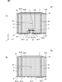
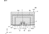
- FIG. 1 is a perspective view of a wireless IC device 101 according to the first embodiment.
- 2A is a plan view of the wireless IC device 101
- FIG. 2B is a right side view of the wireless IC device 101
- FIG. 2C is a bottom view of the wireless IC device 101.
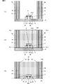
- 3A is a cross-sectional view of the wireless IC device 101
- FIG. 3B is a cross-sectional view of a different part of the wireless IC device 101.
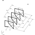
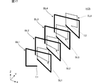
- FIG. 4 is a perspective view schematically showing each conductor portion of the helical coil HC1 included in the wireless IC device 101. As shown in FIG. FIG. FIG.
- FIG. 5A is a perspective view schematically showing a conductor portion of a large-diameter loop provided in the helical coil HC1
- FIG. 5B is a schematic diagram showing a conductor portion of a small-diameter loop provided in the helical coil HC1.
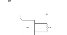
- FIG. 6 is a circuit diagram of the wireless IC device 101.
- FIG. 7A is an enlarged view of the DP1 portion in FIG. 2A
- FIG. 7B is a detailed cross-sectional view along the line AA in FIG. 7A.
- FIG. 8 is a cross-sectional view illustrating the manufacturing process of the wireless IC device 101 in order.
- FIG. 8 is a cross-sectional view illustrating the manufacturing process of the wireless IC device 101 in order.
- FIG. 9 is a cross-sectional view sequentially illustrating the manufacturing process of the wireless IC device 101.
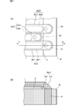
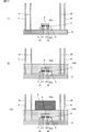
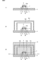
- FIG. 10A is a cross-sectional view of the wireless IC device 102 according to the second embodiment
- FIG. 10B is a cross-sectional view of the wireless IC device 102 taken along line BB in FIG. 10A. is there.
- FIG. 11 is a cross-sectional view illustrating a part of the manufacturing process of the wireless IC device 102 in order.
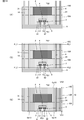
- FIG. 12 is a cross-sectional view of the wireless IC device 103 according to the third embodiment.
- FIG. 13 is a cross-sectional view illustrating the manufacturing process of the wireless IC device 103 in order.
- FIG. 14 is a cross-sectional view sequentially illustrating the manufacturing process of the wireless IC device 103.
- FIG. 15 is a cross-sectional view sequentially illustrating the manufacturing process of the wireless IC device 103.
- FIG. 16 is a cross-sectional view of the wireless IC device 104 according to the fourth embodiment.
- FIG. 17 is a perspective view schematically showing each conductor portion of the helical coil HC5 according to the fifth embodiment.
- FIG. 18A is a perspective view schematically showing a conductor portion of a large-diameter loop provided in the helical coil HC5, and
- FIG. 18B schematically shows a conductor portion of a small-diameter loop provided in the helical coil HC5.
- FIG. 19 is a cross-sectional view of the wireless IC device 106 according to the sixth embodiment.
- FIG. 20 is a cross-sectional view sequentially illustrating the manufacturing process of the wireless IC device 106.
- FIG. 21 is a cross-sectional view sequentially illustrating the manufacturing process of the wireless IC device 106.
- FIG. 22 is a cross-sectional view of the wireless IC device 107 according to the seventh embodiment.
- the helical coils according to some embodiments described below are coil antennas that can be used in, for example, the HF band, the LF band, the UHF band, the SHF band, and the like as magnetic flux radiating elements.
- the helical coil can also be used as an inductor element. Therefore, unless otherwise specified, helical coils according to some embodiments described below are examples of both a coil antenna and an inductor element.
- wireless IC devices according to some embodiments described below include an RFIC, a resin main body, and a helical coil, and are, for example, RFID communication devices such as chip-like RFID tags provided on articles to be managed. .
- the article to which the RFID tag is attached is, for example, portable information terminals such as toys and mobile phones, building materials such as scaffolding materials, and industrial materials such as gas cylinders.
- FIG. 1 is a perspective view of a wireless IC device 101 according to the first embodiment.
- 2A is a plan view of the wireless IC device 101
- FIG. 2B is a right side view of the wireless IC device 101
- FIG. 2C is a bottom view of the wireless IC device 101.
- 3A is a cross-sectional view of the wireless IC device 101
- FIG. 3B is a cross-sectional view of a different part of the wireless IC device 101.
- the first insulating layer 1 and the second insulating layer 2 are hatched for easy understanding of the structure.
- 3A and 3B some thicknesses are exaggerated. The same applies to the sectional views in the following embodiments.
- the protective layer 62 is not shown for easy understanding of the structure.
- the wireless IC device 101 has a rectangular parallelepiped shape whose longitudinal direction coincides with the X-axis direction, and includes a resin main body 10, a helical coil (described in detail later), a first insulating layer 1, a second insulating layer 2, a wiring board 3, An RFIC 4 and protective layers 61 and 62 are provided.
- the resin body 10 has a rectangular parallelepiped shape whose longitudinal direction coincides with the X-axis direction, and has a first surface VS1 and a second surface VS2 facing the first surface VS1.
- the resin body 10 is a thermosetting resin such as an epoxy resin.
- FIG. 4 is a perspective view schematically showing each conductor portion of the helical coil HC1 included in the wireless IC device 101.
- FIG. FIG. 5A is a perspective view schematically showing a conductor portion of a large-diameter loop provided in the helical coil HC1
- FIG. 5B is a schematic diagram showing a conductor portion of a small-diameter loop provided in the helical coil HC1. It is the perspective view shown in. In FIG. 4, the small-diameter loop is shown by a broken line in order to make the structure of the helical coil HC1 easy to understand.
- the helical coil HC1 has a winding axis AX along the first surface VS1 of the resin body 10, and includes a plurality of large diameter loops BL1, BL2, BL3, BL4 and a plurality of small diameter loops SL1, SL2, SL3, SL4.
- the helical coil HC1 has a first portion (described in detail later) embedded in the resin body 10 and a second portion (described in detail later) patterned on the surface of the resin body 10.
- the winding axis AX of the helical coil HC1 according to the present embodiment is parallel to the Y-axis direction.
- the plurality of small-diameter loops SL1, SL2, SL3, SL4 are large-diameter loops BL1, BL2, BL3, as viewed from the Y-axis direction (corresponding to the “winding axis direction” in the present invention) as will be described in detail later. It is arranged inside the outer diameter of BL4.
- each of the small-diameter loops SL1, SL2, SL3, SL4 has substantially the same shape, and is perpendicular to the first surface VS1 of the resin body 10.
- the plurality of small-diameter loops SL1, SL2, SL3, SL4 include first small-diameter columnar conductors 11, 12, 13, 14, second small-diameter columnar conductors 21, 22, 23, 24, first small-diameter conductor patterns Sp11, Sp12, Sp13, Sp14 and second small-diameter conductor patterns Sp21, Sp22, Sp23, Sp24 are included.
- the small-diameter loop SL1 includes a first small-diameter columnar conductor 11, a second small-diameter columnar conductor, a first small-diameter conductor pattern Sp11, and a second small-diameter conductor pattern Sp21.
- the small-diameter loop SL2 includes a first small-diameter columnar conductor 12, a second small-diameter columnar conductor 22, a first small-diameter conductor pattern Sp12, and a second small-diameter conductor pattern Sp22.
- the small-diameter loop SL3 includes a first small-diameter columnar conductor 13, a second small-diameter columnar conductor 23, a first small-diameter conductor pattern Sp13, and a second small-diameter conductor pattern Sp23.
- the small-diameter loop SL4 includes a first small-diameter columnar conductor 14, a second small-diameter columnar conductor, a first small-diameter conductor pattern Sp14, and a second small-diameter conductor pattern Sp24.
- the first small-diameter columnar conductors 11, 12, 13, and 14 and the second small-diameter columnar conductors 21, 22, 23, and 24 are in the Z-axis direction (corresponding to the “direction perpendicular to the first surface” of the resin body in the present invention). And a columnar metal body arranged in the Y-axis direction.
- the first small-diameter columnar conductors 11, 12, 13, 14 and the second small-diameter columnar conductors 21, 22, 23, 24 are embedded in the resin body 10 except for the first and second ends.
- Each of the first small-diameter columnar conductors 11, 12, 13, 14 and the second small-diameter columnar conductors 21, 22, 23, and 24 is, for example, a cylindrical Cu pin.
- a Cu wire having a circular cross section is a predetermined length unit. It is obtained by cutting with.
- the cross-sectional shape may be a rectangle or a polygon.
- the first small-diameter columnar conductors 11, 12, 13, 14 and the second small-diameter columnar conductors 21, 22, 23, 24 are “first portions” of the helical coil HC 1 embedded in the resin body 10. It corresponds to.
- the first small-diameter conductor patterns Sp11, Sp12, Sp13, Sp14 are conductor patterns formed on the first surface VS1 of the resin main body 10 as shown in FIGS. 2A and 2B, and are columnar conductors ( The first small diameter columnar conductor or the second small diameter columnar conductor) is connected to the first end.
- the first small-diameter conductor pattern Sp11 connects the first end of the first small-diameter columnar conductor 12 and the first end of the second small-diameter columnar conductor 21.
- the first small-diameter conductor pattern Sp12 connects the first end of the first small-diameter columnar conductor 13 and the first end of the second small-diameter columnar conductor 22.
- the first small-diameter conductor pattern Sp13 connects the first end of the first small-diameter columnar conductor 14 and the first end of the second small-diameter columnar conductor 23.
- the first small-diameter conductor pattern Sp14 connects the first end of the second small-diameter columnar conductor 24 and the RFIC.
- the first small-diameter conductor patterns Sp11, Sp12, Sp13, and Sp14 are obtained by coating a conductor film formed by printing Ag paste, for example, with a plating film such as Cu.
- 2nd small diameter conductor pattern Sp21, Sp22, Sp23, Sp24 is a conductor pattern formed in the 2nd surface VS2 of the resin main body 10, as shown to FIG. 2 (A) and FIG. 2 (B), and columnar conductor ( The first small-diameter columnar conductor and the second small-diameter columnar conductor are connected to the second end.
- the second small-diameter conductor pattern Sp ⁇ b> 21 connects the second end of the first small-diameter columnar conductor 11 and the second end of the second small-diameter columnar conductor 21.
- the second small-diameter conductor pattern Sp ⁇ b> 22 connects between the second end of the first small-diameter columnar conductor 12 and the second end of the second small-diameter columnar conductor 22.
- the second small-diameter conductor pattern Sp ⁇ b> 23 connects between the second end of the first small-diameter columnar conductor 13 and the second end of the second small-diameter columnar conductor 23.
- the second small-diameter conductor pattern Sp ⁇ b> 24 connects the second end of the first small-diameter columnar conductor 14 and the second end of the second small-diameter columnar conductor 24.
- the second small-diameter conductor patterns Sp21, Sp22, Sp23, Sp24 are, for example, obtained by coating a conductor pattern formed by printing Ag paste with a plating film such as Cu.
- the first small-diameter conductor patterns Sp11, Sp12, Sp13, Sp14 and the second small-diameter conductor patterns Sp21, Sp22, Sp23, Sp24 are “second” of the helical coil HC1 patterned on the surface of the resin body 10. Corresponds to “part”.
- the first insulating layer 1 is formed on the surface of the first surface VS1 of the resin body 10 and the first small-diameter conductor patterns Sp11, Sp12, Sp13, Sp14.
- the first insulating layer 1 is an insulator film that covers at least a part of the surface of the first small-diameter conductor pattern Sp11, Sp12, Sp13, Sp14. In the present embodiment, as shown in FIGS. 2A, 2B, 3C, etc., the first insulating layer 1 covers the entire first small-diameter conductor patterns Sp11, Sp12, Sp13, Sp14. .
- the first insulating layer 1 is a thermosetting resin such as an epoxy resin.
- the first insulating layer 1 is sandwiched between the portions overlapping with (described later in detail).
- the second insulating layer 2 is formed on the surface of the second surface VS2 of the resin main body 10 and the second small-diameter conductor patterns Sp21, Sp22, Sp23, Sp24.
- the second insulating layer 2 is an insulating film that covers at least part of the surface of the second small-diameter conductor pattern Sp21, Sp22, Sp23, Sp24. In the present embodiment, as shown in FIGS. 2A, 2B, 3A, etc., the second insulating layer 2 covers the entire second small-diameter conductor patterns Sp21, Sp22, Sp23, Sp24. .
- the second insulating layer 2 is a thermosetting resin such as an epoxy resin.
- the second small-diameter conductor patterns Sp21, Sp22, Sp23, Sp24 and the second large-diameter conductor patterns Bp21, Bp22, Bp23, Bp24 are sandwiched between the portions overlapping with (described later in detail).
- each of the large-diameter loops BL1, BL2, BL3, BL4 has substantially the same shape and is perpendicular to the first surface VS1 of the resin body 10.
- the plurality of large-diameter loops BL1, BL2, BL3, BL4 include first large-diameter columnar conductors 31, 32, 33, 34, second large-diameter columnar conductors 41, 42, 43, 44, first large-diameter conductor patterns Bp11, Bp12, Bp13, Bp14, Bp15 and second large-diameter conductor patterns Bp21, Bp22, Bp23, Bp24.
- the large diameter loop BL1 includes a first large diameter columnar conductor 31, a second large diameter columnar conductor 41, a first large diameter conductor pattern Bp11, and a second large diameter conductor pattern Bp21.
- the large diameter loop BL2 includes a first large diameter columnar conductor 32, a second large diameter columnar conductor 42, a first large diameter conductor pattern Bp12, and a second large diameter conductor pattern Bp22.
- the large-diameter loop BL3 includes a first large-diameter columnar conductor 33, a second large-diameter columnar conductor 43, a first large-diameter conductor pattern Bp13, and a second large-diameter conductor pattern Bp23.
- the large-diameter loop BL4 includes a first large-diameter columnar conductor 34, a second large-diameter columnar conductor 44, first large-diameter conductor patterns Bp14 and Bp15, and a second large-diameter conductor pattern Bp24.
- the first large-diameter columnar conductors 31, 32, 33, 34 and the second large-diameter columnar conductors 41, 42, 43, 44 are columnar metal bodies that extend in the Z-axis direction and are arranged in the Y-axis direction. is there.
- the first large-diameter columnar conductors 31, 32, 33, and 34 and the second large-diameter columnar conductors 41, 42, 43, and 44 are embedded in the resin body 10 except for the first and second ends.
- Each of the first large-diameter columnar conductors 31, 32, 33, and 34 and the second large-diameter columnar conductors 41, 42, 43, and 44 is, for example, a cylindrical Cu pin. Obtained by cutting in long units.
- the cross-sectional shape may be a rectangle or a polygon.
- the first large-diameter columnar conductors 31, 32, 33, 34 and the second large-diameter columnar conductors 41, 42, 43, 44 are “first” of the helical coil HC 1 embedded in the resin body 10. Corresponds to “part”.
- the first large-diameter conductor patterns Bp11, Bp12, Bp13, Bp14, and Bp15 are formed on the first surface VS1 of the resin body 10 and the surface of the first insulating layer 1 as shown in FIGS. 2 (A) and 2 (B). It is a conductor pattern formed over and connected to the columnar conductor (first large diameter columnar conductor or second large diameter columnar conductor) first end.
- the first large-diameter conductor pattern Bp11 connects the RFIC and the first end of the first large-diameter columnar conductor 31.
- the first large-diameter conductor pattern Bp12 connects the first end of the first large-diameter columnar conductor 32 and the first end of the second large-diameter columnar conductor 41.
- the first large-diameter conductor pattern Bp13 connects the first end of the first large-diameter columnar conductor 33 and the first end of the second large-diameter columnar conductor 42.
- the first large-diameter conductor pattern Bp14 connects the first end of the first large-diameter columnar conductor 34 and the first end of the second large-diameter columnar conductor 43.
- the first large-diameter conductor pattern Bp15 connects the first end of the second large-diameter columnar conductor and the first end of the first small-diameter columnar conductor 11 described above.
- the first large-diameter conductor patterns Bp11, Bp12, Bp13, Bp14, and Bp15 are obtained by coating a conductor pattern formed by printing Ag paste, for example, with a plating film such as Cu.
- the second large-diameter conductor patterns Bp21, Bp22, Bp23, Bp24 are formed across the second surface VS2 and the second insulating layer 2 of the resin body 10, as shown in FIGS. 2 (A) and 2 (B).
- the conductor pattern is connected to the second end of the columnar conductor (the first large-diameter columnar conductor and the second large-diameter columnar conductor).
- the second large-diameter conductor pattern Bp21 connects between the second end of the first large-diameter columnar conductor 31 and the second end of the second large-diameter columnar conductor 41.
- the second large-diameter conductor pattern Bp22 connects the second end of the first large-diameter columnar conductor 32 and the second end of the second large-diameter columnar conductor 42.
- the second large-diameter conductor pattern Bp23 connects the second end of the first large-diameter columnar conductor 33 and the second end of the second large-diameter columnar conductor 43.
- the second large diameter conductor pattern Bp24 connects between the second end of the first large diameter columnar conductor 34 and the second end of the second large diameter columnar conductor 44.
- the second large-diameter conductor patterns Bp21, Bp22, Bp23, and Bp24 are obtained by coating a conductor film formed by printing Ag paste, for example, with a plating film such as Cu.
- the helical coil HC1 in which the first large conductor patterns Bp11, Bp12, Bp13, Bp14, Bp15 and the second large conductor patterns Bp21, Bp22, Bp23, Bp24 are patterned on the surface of the resin body 10. This corresponds to the “second part”.
- the outer diameter dimensions of these small diameter loops SL1, SL2, SL3, SL4 are smaller than the outer diameter dimensions of the large diameter loops BL1, BL2, BL3, BL4 when viewed from the Y-axis direction. Further, the inner diameter dimensions of the small diameter loops SL1, SL2, SL3, SL4 are smaller than the inner diameter dimensions of the large diameter loops BL1, BL2, BL3, BL4 when viewed from the Y-axis direction. And small diameter loop SL1, SL2, SL3, SL4 is arrange
- the small-diameter loops SL1, SL2, SL3, and SL4 are arranged inside the inner diameters of the large-diameter loops BL1, BL2, BL3, and BL4 when viewed from the Y-axis direction.
- the plurality of large-diameter loops BL1, BL2, BL3, BL4 are connected to each other to form a helical large-diameter coil BC of about 4 turns, and the plurality of small-diameter loops SL1, SL2, SL3, SL4 are connected to each other.
- a helical small-diameter SC having about 4 turns is formed.
- the second end Be2 of the large diameter coil BC is connected to the first end Se1 of the small diameter coil SC to constitute the helical coil HC1.
- the extending direction (+ Y direction) from the first end Be1 to the second end Be2 of the large-diameter coil BC in the Y-axis direction is the second from the first end Se1 of the small-diameter coil SC in the Y-axis direction.
- the direction opposite to the extending direction ( ⁇ Y direction) toward the end Se2 is opposite.
- at least a part of the large-diameter loop formation region BFE in the Y-axis direction overlaps the small-diameter loop formation region SFE in the Y-axis direction.
- a plurality of second large-diameter conductor patterns Bp21, Bp22, Bp23, Bp24 and a plurality of second small-diameter conductor patterns Sp21, Sp22, Sp23, Sp24 are represented by Y They are arranged alternately one after another in the axial direction.
- the large-diameter loop and the small-diameter loop are arranged without gaps along the Y-axis direction when viewed from the Z-axis direction (corresponding to “viewing the second surface of the resin main body of the present invention in plan view”).
- the plurality of second small diameter columnar conductors 21, 22, 23, 24 and the plurality of second large diameter columnar conductors 41, 42, 43, 44 are Y They are alternately arranged with respect to the axial direction.
- the plurality of first small-diameter columnar conductors 11, 12, 13, 14 and the plurality of first large-diameter columnar conductors 31, 32, 33, 34 are alternately arranged in the Y-axis direction. Is done.
- the large-diameter loop and the small-diameter loop are along the Y-axis direction when viewed from the X-axis direction (corresponding to the “direction parallel to the first surface and the direction perpendicular to the winding axis direction” in the present invention). Are arranged without gaps.
- the wiring board 3 is a flat plate having a first main surface PS1 and a second main surface PS2 facing the first main surface PS1 and having a rectangular planar shape.
- the wiring board 3 includes mounting electrodes 81 and 82, interlayer connection conductors V1 and V2, and the like.
- the mounting electrodes 81 and 82 are electrodes for mounting the RFIC 4, and are formed on the second main surface PS2 of the wiring board 3.
- the wiring board 3 is a thermosetting printed wiring board such as an epoxy resin, and is typically a double-sided through-hole board.
- the wiring board 3 is not limited to this, and may be a printed wiring board or a ceramic substrate whose base material is a thermoplastic resin such as polyimide resin.
- the wiring board 3 may be a single layer substrate or a multilayer substrate.
- the wiring board 3 is arranged such that the second main surface PS2 is embedded inside the resin body 10 and the first main surface PS1 is exposed from the resin body 10.
- the wiring board 3 is embedded in the resin main body 10 such that the first main surface PS1 of the wiring board 3 and the first surface VS1 of the resin main body 10 are on the same plane.
- the first main surface PS1 and the second main surface PS2 of the wiring board 3 are disposed so as to be parallel to the X-axis direction and the Y-axis direction. That is, the first main surface PS1 and the second main surface PS2 are arranged so as to be parallel to the winding axis of the helical coil HC1.
- the wiring board 3 is disposed inside the large-diameter loops BL1, BL2, BL3, BL4 and the small-diameter loops SL1, SL2, SL3, SL4 as viewed from the Y-axis direction.
- the RFIC 4 is mounted on the second main surface PS2 of the wiring board 3 and embedded in the resin main body 10 as shown in FIGS. 1 and 2A.
- the antenna port of the RFIC 4 is connected to mounting electrodes 81 and 82 formed on the second main surface PS2 of the wiring board 3, respectively.
- the mounting electrodes 81 and 82 are connected to the first end E1 and the second end E2 of the helical coil HC1 shown in FIG. 4 via the interlayer connection conductors V1 and V2, respectively. That is, the RFIC 4 is connected to the first end and the second end of the helical coil HC1, respectively.
- the RFIC 4 is, for example, a packaged RFIC.
- the RFIC 4 may be a bare chip RFIC chip.
- the RFIC chip and the mounting electrodes 81 and 82 (land pattern) may be connected by a wire.
- the protective layers 61 and 62 are formed on the first surface VS ⁇ b> 1 and the second surface VS ⁇ b> 2 of the resin main body 10, and are provided with a conductor pattern (first large diameter conductor pattern, second large diameter conductor pattern, first small diameter conductor pattern, second small diameter). The formation surface of the conductor pattern is covered.
- the protective layers 61 and 62 are resin films provided for the purpose of preventing oxidation of the conductor pattern, improving heat resistance, and preventing short-circuiting between conductors due to metal foreign matter, and are, for example, solder resist films.
- the protective layers 61 and 62 are not essential.
- FIG. 6 is a circuit diagram of the wireless IC device 101.
- the wireless IC device 101 includes, for example, an HF band RFIC for an HF band RFID system.
- the helical coil HC1 is connected to the RFIC 4, and an LC resonance circuit is configured by the helical coil HC1 and the capacitive component of the RFIC 4. Its resonant frequency is substantially equal to the communication frequency of the RFID system.
- the communication frequency band is, for example, the 13.56 MHz band.
- the “wireless IC device” may be composed of a helical coil HC1 and an RFIC chip, or an integrated module in which an RFIC chip is mounted on a substrate provided with a helical coil HC1 and a matching circuit. And may be configured.
- An “RFID tag” includes an RFIC and a helical coil connected to the RFIC, and is an information medium that reads and writes data in a built-in memory in a non-contact manner using radio waves (electromagnetic waves) or magnetic fields. It is defined as That is, the wireless IC device of this embodiment is configured as an RFID tag.
- FIG. 7A is an enlarged view of the DP1 portion in FIG. 2A
- FIG. 7B is a detailed cross-sectional view along the line AA in FIG. 7A. 7A and 7B, the protective layer 62 is not shown for easy understanding of the structure.
- the large-diameter conductor pattern and the small-diameter conductor pattern include a base electrode layer formed on the surface of the resin body 10 and a plating electrode layer laminated on the base electrode layer.
- the second large-diameter conductor pattern Bp21 shown in FIG. 7A will be described as an example.
- the second large-diameter conductor pattern Bp21 includes a base electrode layer BA1 and a plating electrode layer BC1, and the base electrode layer BA1 is an end.
- the line width of the portion is smaller than the diameter of the upper end surface of the second large-diameter columnar conductor 41.
- the end portion of the base electrode layer BA1 is formed so as to cover a part of the upper end surface of the second large-diameter columnar conductor 41.
- the plating electrode layer BC1 is formed so as to cover the upper end surface of the second large-diameter columnar conductor 41 that is not covered with the base electrode layer BA1 and the base electrode layer BA1.
- the base electrode layer is formed by screen printing a conductive paste such as Ag.
- a plating electrode layer is a plating film which coat
- the large-diameter conductor pattern and the small-diameter conductor pattern can all be made thicker by forming a Cu plating film. Therefore, the DCR of the helical coil can be further reduced.
- the columnar conductor is a Cu pin
- the plated electrode layer which is a Cu plating film, covers not only the base electrode layer but also the upper end surface of the columnar conductor not covered by the base electrode layer. It is formed. Therefore, with this configuration, the bonding strength of the large-diameter conductor pattern and the small-diameter conductor pattern and the columnar conductor is greater than when the base electrode layer, which is an Ag conductor pattern, is coated on the entire upper end surface of the columnar conductor that is a Cu pin. Can be high.
- the wireless IC device 101 according to the present embodiment has the following effects.
- (A) In the present embodiment, at least a portion where the small diameter conductor pattern (first small diameter conductor pattern, second small diameter conductor pattern) and the large diameter conductor pattern (first large diameter conductor pattern, second large diameter conductor pattern) overlap. Insulating layers (first insulating layer, second insulating layer) are sandwiched. In this configuration, the small-diameter conductor pattern and the large-diameter conductor pattern are not formed on the same plane, and an insulating layer is interposed between the small-diameter conductor pattern and the large-diameter conductor pattern. The possibility of contact with the conductor pattern (short circuit between lines) is low.
- the large-diameter conductor pattern and the small-diameter conductor pattern are ensured without separately providing a connection member such as a jumper chip. Therefore, the large-diameter loop and the small-diameter loop can be arranged at a narrow pitch in the Y-axis direction, and it becomes easy to obtain a helical coil having a desired number of turns and a desired inductance value.
- the small-diameter conductor pattern and the large-diameter conductor pattern partially overlap each other when viewed from the Z-axis direction, so that the line width of the small-diameter conductor pattern and the large-diameter conductor pattern can be easily increased, and the helical coil HC1 DCR can be further reduced.
- the large-diameter loops BL1, BL2, BL3, and BL4 and the small-diameter loops SL1, SL2, SL3, and SL4 constituting the helical coil HC1 are formed of columnar conductors. . Therefore, the DCR of the large-diameter loop and the small-diameter loop can be reduced as compared with the case where the sintered metal body is formed by firing the conductive paste, or the thin-film metal body is formed by etching the conductive thin film. A lossy helical coil is obtained. Further, since the resistance of the entire helical coil can be reduced, a highly sensitive wireless IC device or a small wireless IC device for high sensitivity can be obtained.
- the radial columnar conductors are arranged in the Y-axis direction and arranged in a staggered manner as viewed from the Z-axis direction.
- insulation between adjacent large-diameter conductor patterns and small-diameter conductor patterns is ensured without separately providing a connection member such as a jumper chip. Therefore, the large diameter loop and the small diameter loop can be arranged at a narrow pitch in the Y-axis direction.
- a large-diameter conductor pattern (first large-diameter conductor pattern and second large-diameter conductor pattern) and a small-diameter conductor pattern (first) used for a part of the large-diameter loop and a part of the small-diameter loop.
- the small-diameter conductor pattern and the second small-diameter conductor pattern are conductor patterns formed on the surface of the resin body 10 and the like, not wires or the like.
- the possibility of contact (short between lines) between adjacent large-diameter conductor patterns or between adjacent small-diameter conductor patterns is low, so the gap between large-diameter conductor patterns arranged in the Y-axis direction can be easily reduced.
- the gap between the small-diameter conductor patterns arranged in the Y-axis direction can be easily reduced.
- the desired number of turns and the desired inductance value can be obtained even if the occupation area (dimension in the Y-axis direction) is the same. It becomes easy to obtain the helical coil which has.
- the mounting electrode 81 of the RFIC 4 , 82 (land pattern) or the like hardly interferes with the formation of the magnetic field of the helical coil HC1. Further, the adverse effect (malfunction, unstable operation, etc.) on the RFIC 4 due to the magnetic field of the helical coil HC1 is small. Furthermore, the adverse effect on the helical coil due to noise generated from the digital circuit section of the RFIC 4 (decrease in reception sensitivity, wraparound of the transmission signal to the reception circuit, etc.) is small.
- the RFIC 4 is arranged inside the helical coil. Therefore, the protection function of the RFIC 4 is high. Further, since the RFIC 4 is not exposed to the outside of the wireless IC device 101, an increase in size due to mounting the RFIC 4 outside the helical coil can be avoided.
- the wireless IC device 101 includes a surface-mounted component such as the RFIC 4, a part of the large-diameter loop (first large-diameter columnar conductor, second large-diameter columnar conductor), and a part of the small-diameter loop (first small-diameter columnar conductor, Since the second small-diameter columnar conductor) is protected by the resin body 10, the entire wireless IC device is robust.
- the wireless IC device is embedded in a resin molded article, the solder connection portion of the surface mount chip component is protected against a high temperature resin (for example, a high temperature resin of 300 ° C. or higher) that flows during injection molding.
- a high temperature resin for example, a high temperature resin of 300 ° C. or higher
- the RFIC 4 includes the large-diameter loops BL1, BL2, BL3, BL4, the small-diameter loops SL1, SL2, SL3, SL4, the first large-diameter conductor patterns Bp11, Bp12, Bp13, Bp14, Bp15, Two large-diameter conductor patterns Bp21, Bp22, Bp23, Bp24, the first small-diameter conductor patterns Sp11, Sp12, Sp13, Sp14 and the second small-diameter conductor patterns Sp21, Sp22, Sp23, Sp24, and the like, and Surrounded by the resin body 10 and the wiring board 3.
- the resin body 10 and the wiring board 3 are bonded together by joining the resins, and the surface-mounted components and small-diameter loops do not come off or deform, so after cooling The soldered joint will return to normal. Therefore, the inductance value of the helical coil can be maintained.
- the wireless IC device 101 has a large-diameter conductor pattern constituting a large-diameter loop (first large-diameter conductor patterns Bp11, Bp12, Bp13, Bp14, Bp15 and second large-diameter conductor patterns Bp21, Bp22, Bp23, Bp24). Is formed over the surface of the resin body 10 and the surfaces of the insulating layers (the first insulating layer 1 and the second insulating layer 2). Therefore, the substantial opening diameter of the helical coil HC1 is large.
- a helical coil (coil antenna) having a size substantially equal to the size of the chip-shaped wireless IC device 101 can be configured, and a large communication distance is ensured despite being a small chip-shaped component.
- communication can be performed with a relatively wide positional relationship with respect to the antenna of the communication partner.
- the first small-diameter conductor patterns Sp11, Sp12, Sp13, Sp14 and the second small-diameter conductor patterns Sp21, Sp22, Sp23, Sp24 are formed on the surface of the resin body 10 by patterning. Therefore, the connection between the first ends of the first small-diameter columnar conductors 11, 12, 13, 14 and the first ends of the second small-diameter columnar conductors 21, 22, 23, 24, and the first small-diameter columnar conductors 11, 12, 13 , 14 and the second ends of the second small-diameter columnar conductors 21, 22, 23, 24 are facilitated.
- the first large-diameter conductor patterns Bp11, Bp12, Bp13, Bp14, Bp15, and the second large-diameter conductor pattern Bp21, over the surface of the resin main body 10 and the surface of the insulating layer, are patterned.
- Bp22, Bp23, and Bp24 are formed.
- connection between the second ends of 32, 33, and 34 and the second ends of the second large-diameter columnar conductors 41, 42, 43, and 44 is facilitated.
- the first large-diameter conductor pattern Bp11, Bp12, Bp13, Bp14, Bp15, the second large-diameter conductor pattern Bp21, Bp22, Bp23, extending in the X-axis direction, Bp24, the first small-diameter conductor patterns Sp11, Sp12, Sp13, Sp14 and the second small-diameter conductor patterns Sp21, Sp22, Sp23, Sp24 can all be made thick by forming a plating film of Cu or the like. Therefore, the DCR of the helical coil can be further reduced.
- the extending direction (+ Y direction) from the first end Be1 to the second end Be2 of the large-diameter coil BC in the Y-axis direction is the same as that of the small-diameter coil SC in the Y-axis direction.
- the extending direction ( ⁇ Y direction) from the first end Se1 to the second end Se2 is opposite to the extending direction.
- at least a part of the large-diameter loop formation region BFE in the Y-axis direction overlaps the small-diameter loop formation region SFE in the Y-axis direction.
- a helical coil having a small occupied area (particularly the dimension in the Y-axis direction) relative to the number of turns can be realized. Also, with this configuration, the conductor that does not contribute to inductance can be shortened, so that the DCR of the helical coil can be further reduced.
- the wireless IC device 101 has a structure in which the wiring board 3 is embedded in the resin main body 10 so that the first main surface PS1 of the wiring board 3 and the first surface VS1 of the resin main body 10 are on the same plane.
- the first small-diameter conductor pattern, the first large-diameter conductor pattern, and the like formed over the first surface VS1 and the first main surface PS1 can be easily formed by patterning, the first end of the helical coil HC1 And the connection between the second end and the RFIC 4 is facilitated.
- the large-diameter loops BL1, BL2, BL3, and BL4 and the small-diameter loops SL1, SL2, SL3, and SL4 are arranged without gaps along the Y-axis direction when viewed from the Z-axis direction.
- the magnetic flux generated in the helical coil is difficult to leak from the gap between the large-diameter loop and the small-diameter loop that are adjacent to each other. Therefore, a helical coil having a high inductance value can be configured.
- magnetic field coupling can be performed with a relatively wide positional relationship with respect to the coil antenna on the communication partner side.
- the edge in the Y-axis direction of the large-diameter loop and the edge in the Y-axis direction of the small-diameter loop are viewed from the Z-axis direction.
- the end portion preferably overlaps partly (see FIG. 2A).
- the large-diameter loops BL1, BL2, BL3, and BL4 and the small-diameter loops SL1, SL2, SL3, and SL4 are arranged without gaps along the Y-axis direction when viewed from the X-axis direction. Yes.
- this configuration makes it possible to configure a helical coil having a high inductance value. Further, when a helical coil is used as a coil antenna, magnetic field coupling can be performed with a relatively wide positional relationship with respect to the coil antenna on the communication partner side.
- the edge in the Y-axis direction of the large-diameter loop and the edge in the Y-axis direction of the small-diameter loop are viewed from the X-axis direction.
- the end portion preferably overlaps partly (see FIG. 2B).
- the helical coil HC1 including the large-diameter coil BC of about 4 turns and the small-diameter coil SC of about 4 turns is shown, but the present invention is not limited to this.
- the number of turns of the large-diameter coil BC and the number of turns of the small-diameter coil can be appropriately changed as long as they are larger than one.
- the configuration in which one large-diameter coil BC and one small-diameter coil SC are connected is shown, but the present invention is not limited to this.
- a plurality of large-diameter coils and a plurality of small-diameter coils may be alternately and sequentially connected.
- the number of large diameter coils and the number of small diameter coils do not need to be the same number.
- the plurality of large-diameter coils may have different numbers of turns, and the plurality of small-diameter coils may have different numbers of turns.
- the wiring board 3 on which the RFIC 4 is mounted is prepared. Specifically, mounting electrodes 81 and 82 (for mounting the RFIC 4 on the second main surface PS2 of the wiring board 3 having the first main surface PS1 and the second main surface PS2 opposed to the first main surface PS1. Land pattern) or the like. Further, in the thickness direction of the wiring board 3, interlayer connection conductors V 1 and V 2 formed inside the wiring board 3 and connected to the mounting electrodes 81 and 82 are formed.
- the conductive bonding material 5 such as a solder paste is formed on the mounting electrodes 81 and 82 for mounting the RFIC 4. At this time, the conductor pattern is not formed on the first main surface PS1 side of the wiring board 3.
- the wiring board 3 is a printed wiring board based on a thermosetting resin such as a glass epoxy board or an epoxy resin, for example, but a thick film pattern is formed on a board or ceramic board based on a thermoplastic resin such as a polyimide resin. May be formed.
- the wiring board 3 may be a single layer substrate or a multilayer substrate.
- the mounting electrodes 81 and 82 are formed by patterning a metal foil having a small specific resistance, such as Cu or Ag.
- the mounting electrodes 81 and 82 are formed by patterning a plating film on the second main surface PS2 of the wiring board 3, or patterning a conductor paste. It may be what you did.
- the mounting electrodes 81 and 82 have a cross-sectional dimension of 18 ⁇ m ⁇ 100 ⁇ m. After performing these patterning, it is preferable that the total film thickness is increased to 40 to 50 ⁇ m by plating with Cu or the like.
- the interlayer connection conductors V1 and V2 are through holes in which a plating film is provided on the inner wall of a through hole that penetrates the wiring board 3, for example.
- the RFIC 4 is mounted on the second main surface PS2 of the wiring board 3 via the conductive bonding material 5 such as solder. Specifically, after mounting components such as RFIC4 on the second main surface PS2 of the wiring board 3 with a mounter, these components are soldered by a reflow process. By this step, the RFIC 4 is electrically connected to the wiring board 3 and is structurally bonded.
- RFIC4 is a packaged RFIC for RFID tags. Further, the RFIC 4 may be a bare chip RFIC chip.
- a support base 6 having an adhesive layer on the main surface is prepared, and the wiring board 3 on which the RFIC 4 is mounted is mounted on the support base 6.
- the first main surface PS1 side of the wiring board 3 is fixed to the support layer 6 with the adhesive layer side.
- the adhesive layer included in the support base 6 is, for example, an adhesive resin.
- This process of mounting the RFIC 4 on the support base 6 is an example of the “first process” in the present invention.
- the first end sides of the columnar conductors (the first small-diameter columnar conductor 14 and the like, the second small-diameter columnar conductor 24 and the like, the first large-diameter columnar conductor 31 and the second large-diameter columnar conductor 41 and the like)
- the support base 6 is fixed to stand on the adhesive layer side.
- each columnar conductor is mounted in a state in which the first end side of each columnar conductor is firmly fixed to the support base 6 via the adhesive layer.
- Each columnar conductor is a columnar post made of Cu.
- the columnar conductors are not limited to those containing Cu as the main component, but those containing Cu as the main component are preferable in terms of conductivity and workability.
- This step of standing the first end of each of the first small-diameter columnar conductor, the second small-diameter columnar conductor, the first large-diameter columnar conductor, and the second large-diameter columnar conductor on the support base 6 is the “second step in the present invention. Is an example.
- a resin body 10 is formed (coated with resin). Specifically, the resin body 10 coated with epoxy resin or the like at a predetermined height (at least the height of the columnar conductor) on the support base 6 is ground together with the columnar conductor as shown in (4) of FIG. The second end of the columnar conductor is exposed from the second surface VS2 of the resin main body 10 by planarly grinding (or cutting or polishing) the line PL1.
- an epoxy resin or the like is applied to a predetermined height (below the height of the columnar conductor), and then the resin main body 10 is ground (or cut or polished) together with the columnar conductor in a second manner.
- the second end of the columnar conductor may be exposed on the surface VS2.
- the resin main body 10 may be provided by applying a liquid resin, or may be provided by stacking semi-cured sheet-like resins.
- the RFIC 4 After the first step and the second step, the RFIC 4, the first small-diameter columnar conductor 14, etc., the second small-diameter columnar conductor 24, etc., the first large-diameter columnar conductor 31, etc., the second large-diameter columnar conductor 41, etc.
- This step of covering the resin main body 10 to a height at which at least a part of each of them is buried is an example of the “third step” in the present invention.
- the support base 6 is removed from the resin body 10, and the first ends of the columnar conductors, the interlayer connection conductors V1, V2, and the like are replaced with the resin body. It is exposed from the first surface VS1 of 10 and the first main surface PS1 of the wiring board 3.
- the resin main body 10 is ground (or cut, polished) in a planar manner to the grinding line PL2 indicated by (5) in FIG. 9 together with the support base 6, the wiring board 3, and the columnar conductor.
- the first ends of the columnar conductors and the interlayer connection conductors V1 and V2 are exposed from the first surface VS1 of the resin body 10 and the first main surface PS1 of the wiring board 3.
- This step of removing the support base 6 from the resin body 10 after the third step is an example of the “seventh step” in the present invention.
- the second surface VS ⁇ b> 2 of the resin body 10 has a second end such as the first small-diameter columnar conductor 14 and a second end such as the second small-diameter columnar conductor 24.
- a second small-diameter conductor pattern Sp24 or the like that connects the two is formed.
- a conductive paste such as Ag is screen-printed on the second surface VS2 of the resin body 10 where the second ends of the first small diameter columnar conductors 14 and the like and the second ends of the second small diameter columnar conductors 24 and the like are exposed. Thereby, the second small-diameter conductor pattern Sp24 and the like are formed.
- a plating film on the second small-diameter conductor pattern Sp24 or the like by plating with Cu or the like.
- an Au plating film may be further formed on the surface of a plating film such as Cu.
- the thickness of the second small-diameter conductor pattern Sp24 and the like is obtained by immersing the resin body 10 in the plating solution. Can be selectively thickened.
- the second small-diameter conductor pattern Sp24 and the like connecting the second end of the first small-diameter columnar conductor 14 and the second end of the second small-diameter columnar conductor 24 and the like are formed on the second surface VS2.
- This step is an example of the “fourth step” in the present invention.
- the first surface VS1 of the resin body 10 is connected to at least one of the first end of the first small-diameter columnar conductor 14 and the first end of the second small-diameter columnar conductor.
- First small-diameter conductor patterns Sp13, Sp14 and the like are formed.
- the first small-diameter conductor pattern Sp14 connects the second small-diameter columnar conductor 24 and the interlayer connection conductor V2 provided on the wiring board 3.
- a conductive paste such as Ag is screen-printed on the first surface VS1 of the resin body 10 where the first end of the first small-diameter columnar conductor 14 and the first end of the second small-diameter columnar conductor 24 and the like are exposed.
- the first small-diameter conductor patterns Sp13, Sp14, etc. are formed.
- a plating film on the first small-diameter conductor patterns Sp13, Sp14, etc. by plating with Cu or the like.
- an Au plating film may be further formed on the surface of a plating film such as Cu.
- the first small-diameter conductor patterns Sp13, Sp14 and the like are exposed on the outer surface of the resin body 10, the first small-diameter conductor patterns Sp13, Sp13, etc. are immersed in the plating solution.
- the thickness of Sp14 or the like can be selectively increased.
- the first small-diameter conductor pattern Sp14 and the like connected to at least one of the first end of the first small-diameter columnar conductor 14 and the first end of the second small-diameter columnar conductor are formed on the first surface VS1.
- This step is an example of the “eighth step” in the present invention.
- the second insulating layer 2 is formed on at least part of the surface of the second small-diameter conductor pattern Sp24 and the like.
- the second insulating layer 2 is an insulator film that covers the surface of the second small-diameter conductor pattern Sp24 and the like, and is a thermosetting resin such as an epoxy resin, for example.
- This step of forming the second insulating layer 2 on at least a part of the surface of the second small-diameter conductor pattern Sp24 after the fourth step is an example of the “fifth step” in the present invention.
- the first insulating layer 1 is formed on at least part of the surface of the first small-diameter conductor pattern Sp14 and the like.
- the first insulating layer 1 is an insulator film that covers the surface of the first small-diameter conductor pattern Sp14 and the like, and is a thermosetting resin such as an epoxy resin, for example.
- This step of forming the first insulating layer 1 on at least a part of the surface of the first small-diameter conductor pattern Sp14 after the eighth step is an example of the “ninth step” in the present invention.
- the second end VS2 of the first large-diameter columnar conductor 31 and the second large-diameter are formed on the second surface VS2 of the resin body 10 and the surface of the second insulating layer 2.
- a second large-diameter conductor pattern Bp21 and the like that connect between the second ends of the columnar conductors 41 and the like are formed.
- Ag or the like is formed on the second surface VS2 and the surface of the second insulating layer 2 where the second end of the first large-diameter columnar conductor 31 and the second end of the second large-diameter columnar conductor 41 and the like are exposed.
- the second large-diameter conductor pattern Bp21 and the like are formed by screen printing a conductive paste.
- a plating film on the second large-diameter conductor pattern Bp21 or the like by plating with Cu or the like.
- an Au plating film may be further formed on the surface of a plating film such as Cu.
- the thickness of the second large-diameter conductor pattern is selected by immersing the resin body 10 in the plating solution. Can be thickened.
- the second surface VS2 and the surface of the second insulating layer 2 are connected between the second end of the first large-diameter columnar conductor 31 and the second end of the second large-diameter columnar conductor 41 and the like.
- This step of forming the second large-diameter conductor pattern Bp21 and the like is an example of the “sixth step” in the present invention.
- the first end VS1 of the first large-diameter columnar conductor 31 and the second large-diameter columnar shape are formed on the first surface VS1 and the surface of the first insulating layer 1 of the resin body 10.
- a first large-diameter conductor pattern Bp11 or the like connected to at least one of the first ends of the conductor 41 or the like is formed.
- a connection conductor 71 that connects the first large-diameter columnar conductor 31 and the interlayer connection conductor V ⁇ b> 1 provided on the wiring board 3 is formed on the first surface VS ⁇ b> 1 and the surface of the first insulating layer 1.
- the first large-diameter conductor patterns Bp11, Bp12, etc. are formed by screen printing the conductive paste.
- a plating film on the first large-diameter conductor patterns Bp11, Bp12, etc. by plating with Cu or the like.
- an Au plating film may be further formed on the surface of a plating film such as Cu.
- the first large-diameter conductor patterns Bp11, Bp12 and the like are exposed on the outer surface of the resin body 10, the first large-diameter conductor pattern is immersed in the plating solution.
- the thicknesses of Bp11, Bp12, etc. can be selectively increased.
- the first surface VS1 and the surface of the first insulating layer 1 are connected to at least one of the first end of the first large-diameter columnar conductor 31 and the first end of the second large-diameter columnar conductor 41 and the like.
- This step of forming the first large-diameter conductor pattern Bp11 and the like is an example of the “tenth step” in the present invention.
- the conductor patterns (the first large-diameter conductor pattern Bp11 and the like, the second large-diameter conductor pattern Bp21 and the like, the first small-diameter conductor patterns Sp13 and Sp14, and the like, the second small-diameter conductor pattern Sp24, as necessary. And the like) are formed on the formation surface (first surface VS1 and second surface VS2).
- the protective layers 61 and 62 are, for example, a protective resin film (such as a solder resist film) for preventing oxidation.
- the above process is processed in the mother substrate state. After the above steps, the mother board is separated into individual wireless IC devices 101 (pieces).
- the wireless IC device 101 having a small helical coil having a desired inductance value and excellent electrical characteristics, and particularly capable of reducing a direct current resistance.
- the columnar conductor can be firmly fixed using the support base 6 having the adhesive layer. Therefore, a columnar conductor having a small diameter can also be used for manufacturing a helical coil, and a helical coil having a large number of turns and a high inductance can be manufactured.
- Second Embodiment a wireless IC device 102 including resin blocks 7A and 7B and a resin layer 10E is shown. Other configurations are substantially the same as those of the wireless IC device 101.
- FIG. 10A is a cross-sectional view of the wireless IC device 102 according to the second embodiment
- FIG. 10B is a cross-sectional view of the wireless IC device 102 taken along line BB in FIG. 10A. is there.
- the resin main body 10 includes resin blocks 7A and 7B and a resin layer 10E.
- the resin block 7A has a rectangular parallelepiped shape whose longitudinal direction coincides with the Z-axis direction, and the first small-diameter columnar conductor 14 and the like and the first large-diameter columnar conductor 31 and the like covered with an insulator are embedded therein.
- the first small-diameter columnar conductor 14 and the like and the first large-diameter columnar conductor 31 and the like embedded in the resin block 7A are arranged so as to extend in the Z-axis direction, and the first and second ends of the resin block 7A It is exposed from the longitudinal surface.
- the resin block 7B has a rectangular parallelepiped shape whose longitudinal direction coincides with the Z-axis direction, and the second small-diameter columnar conductor 24 and the second large-diameter columnar conductor 41 and the like covered with an insulator are embedded.
- the second small-diameter columnar conductor 24 and the like and the second large-diameter columnar conductor 41 and the like embedded in the resin block 7B are arranged so as to extend in the Z-axis direction, and each of the first end and the second end of the resin block 7B. It is exposed from the longitudinal surface.
- the resin layer 10E has a rectangular parallelepiped shape whose longitudinal direction matches the Z-axis direction.
- the resin blocks 7A and 7B and the resin layer 10E are thermosetting resins such as epoxy resins, and the insulator covered with the columnar conductors is polyurethane, for example.
- the wireless IC device 102 according to the present embodiment has the following effects in addition to the effects described in the first embodiment.
- the wireless IC device 102 according to the present embodiment includes the resin blocks 7A and 7B in which the columnar conductors are embedded, as will be described in detail later, the wireless IC device 102 according to the first embodiment
- the gap between adjacent columnar conductors can be reduced. Therefore, with this configuration, the area occupied by the coil (dimensions in the X-axis direction and the Y-axis direction) can be further reduced for the number of turns. Further, with this configuration, it is possible to easily form a wireless IC device in which the helical coil has a large coil opening.
- the columnar conductors embedded in the resin blocks 7A and 7B are covered with an insulator, the possibility of an electrical short circuit is low even if adjacent columnar conductors come into contact with each other. That is, in this embodiment, the columnar conductors embedded in the resin blocks 7A and 7B may be bundled and in contact with each other.
- the wireless IC device 102 according to the present embodiment is manufactured by, for example, the following process.
- FIG. 11 is a cross-sectional view sequentially illustrating a part of the manufacturing process of the wireless IC device 102.
- the wiring board 3 and the resin blocks 7A and 7B on which the RFIC 4 is mounted on the second main surface PS2 are mounted on the support base 6 having the adhesive layer on the main surface.
- the resin blocks 7A and 7B include columnar conductors coated with an insulator (the first small-diameter columnar conductor 14, etc., the second small-diameter columnar conductor 24, etc., the first large-diameter columnar conductor 31, etc., the second large-diameter columnar conductor 41, etc. ) Is buried.
- the wiring board 3 is fixed so that the first main surface PS1 side of the wiring board 3 is the adhesive layer side of the support base 6, and the first end of each columnar conductor is set to the adhesive layer side of the support base 6 (this book It corresponds to “first step” and “second step” in the invention).
- the resin blocks 7A and 7B can be obtained by embedding a Cu wire covered with an insulator such as polyurethane in a thermosetting resin such as an epoxy resin and cutting it in predetermined length units.
- the resin layer 10E is formed on the support base 6 to the same height as the columnar conductor. Specifically, an epoxy resin or the like is applied to a portion other than the resin blocks 7A and 7B on the support base 6 to a predetermined height (at least the height where the RFIC 4 and the resin blocks 7A and 7B are embedded). Resin layer 10E is formed. Thereafter, the resin blocks 7A and 7B and the resin layer 10E are ground (or cut and polished) to the grinding line PL1 shown in (2) in FIG. The second end of the columnar conductor is exposed (corresponding to the “third step” in the present invention).
- the support base 6 is removed from the resin body 10, and the first ends of the columnar conductors and the interlayer connection conductors V ⁇ b> 1 and V ⁇ b> 2 are replaced with the first of the resin body 10.
- the surface VS1 and the first main surface PS1 of the wiring board 3 are exposed.
- the resin blocks 7A and 7B and the resin layer 10E are ground (or cut or polished) in a plane up to the grinding line PL2 shown in (2) in FIG. 11 together with the support base 6, the wiring board 3, and the columnar conductor.
- the subsequent manufacturing process is the same as that shown in FIGS. 9 (5) to (7) in the first embodiment.
- the manufacturing method uses the resin blocks 7A and 7B in which the columnar conductors are embedded in advance, the columnar conductors can be more easily attached to the support base 6 than the manufacturing method of the wireless IC device 101 shown in the first embodiment. Can stand. In addition, the columnar conductor can be more firmly fixed to the support base 6 having the adhesive layer.
- a wireless IC device 103 including a magnetic core 8 is shown. Other configurations are substantially the same as those of the wireless IC device 101.
- FIG. 12 is a cross-sectional view of the wireless IC device 103 according to the third embodiment.
- the resin main body 10 has a sintered magnetic core 8 such as a ferrite sintered body that acts as a magnetic core for the helical coil.
- the resin main body 10 has resin layers 10A, 10B, and 10C that are nonmagnetic materials.
- the wireless IC device 103 according to the present embodiment has the following effects in addition to the effects described in the first embodiment.
- a wireless IC device including a helical coil having an intended inductance value can be obtained without increasing the size of the helical coil.
- the desired inductance value can be obtained even if the wireless IC device is low-profile.
- the wireless IC device 103 according to the present embodiment is manufactured, for example, by the following process. 13, 14, and 15 are cross-sectional views sequentially illustrating the manufacturing process of the wireless IC device 103.
- the wiring board 3 in which the RFIC 4 is mounted on the second main surface PS2 the columnar conductor (the first small diameter columnar conductor 14, etc. 2 small-diameter columnar conductor 24, etc., first large-diameter columnar conductor 31, etc. and second large-diameter columnar conductor 41, etc.) are mounted.
- the wiring board 3 is fixed so that the first main surface PS1 side of the wiring board 3 is the adhesive layer side of the support base 6, and the first end of each columnar conductor is set to the adhesive layer side of the support base 6 (this book It corresponds to “first step” and “second step” in the invention).
- a nonmagnetic resin layer 10 ⁇ / b> A is formed on the support base 6. Specifically, the resin layer 10 ⁇ / b> A is formed (covered with resin) on the support base 6 to a predetermined height (at least a height at which a part of the RFIC 4 and the columnar conductor is embedded). Thereby, the RFIC 4 is embedded in the resin layer 10A.
- the magnetic core 8 is preferably a ferrite sintered body that is small and has a high magnetic permeability (for example, a relative magnetic permeability of about 50 to 300).
- the magnetic core 8 may be placed before the resin layer 10A is cured.
- the resin layer 10B such as an epoxy resin is coated up to the thickness of the magnetic core 8.
- the resin layer 10C is formed (covered with resin) to the same height as the columnar conductor.
- the resin layer 10C coated with an epoxy resin or the like at a predetermined height is planarly provided to the grinding line PL1 shown in (5) in FIG.
- the second end of the columnar conductor is exposed from the second surface VS2 of the resin body 10 (corresponding to the “third step” in the present invention).
- the support base 6 is removed from the resin body 10, and the first ends of the columnar conductors and the interlayer connection conductors V1, V2, etc. are connected to the first surface VS1 and the wiring of the resin body 10.
- the plate 3 is exposed from the first main surface PS1.
- the resin layer 10A is ground (or cut or polished) in a planar manner to the grinding line PL2 indicated by (5) in FIG. 14 together with the support base 6, the wiring board 3, and the columnar conductor.
- the first ends of the columnar conductors and the interlayer connection conductors V1 and V2 are exposed from the first surface VS1 of the resin body 10 and the first main surface PS1 of the wiring board 3 (corresponding to “seventh step” in the present invention). .
- the second end VS2 of the resin body 10 is connected to the second end of the first small diameter columnar conductor 14 and the second end of the second small diameter columnar conductor 24 and the like.
- a second small-diameter conductor pattern Sp21 or the like that connects the two is formed (corresponding to the “fourth step” in the present invention).
- At least one of the first end of the first small diameter columnar conductor 14 and the first end of the second small diameter columnar conductor 24 and the like is formed on the first surface VS1 of the resin body 10.
- First small-diameter conductor patterns Sp13, Sp14, and the like connected to are formed (corresponding to “eighth step” in the present invention).
- the second insulating layer 2 is formed on at least part of the surface of the second small-diameter conductor pattern Sp21 and the like (corresponding to the “fifth step” in the present invention). ).
- the first insulating layer 1 is formed on at least a part of the surface of the first small-diameter conductor pattern Sp13 or the like (corresponding to “the ninth step” in the present invention).
- the second end of the first large-diameter columnar conductor 31 and the second large diameter are formed on the second surface VS2 of the resin body 10 and the surface of the second insulating layer 2.
- a second large-diameter conductor pattern Bp21 and the like that connect between the second ends of the columnar conductors 41 and the like are formed (corresponding to “sixth step” in the present invention).
- the first end VS1 of the first large-diameter columnar conductor 31 and the second large-diameter columnar shape are formed on the first surface VS1 and the surface of the first insulating layer 1 of the resin body 10.
- First large-diameter conductor patterns Bp11, Bp12 and the like connected to at least one of the first ends of the conductor 41 and the like are formed (corresponding to the “tenth step” in the present invention).
- the conductor pattern (first large-diameter conductor pattern Bp11, etc., second large-diameter conductor pattern Bp21, etc., first small-diameter conductor patterns Sp13, Sp14, etc., second small-diameter conductor pattern Sp24, etc.) ) Are formed on the formation surface (first surface VS1 and second surface VS2).
- the protective layers 61 and 62 are, for example, a protective resin film (such as a solder resist film) for preventing oxidation.
- the above process is processed in the mother substrate state. After the above process, the mother board is separated into individual wireless IC devices 103 (pieces).
- Fourth Embodiment shows about the radio
- Other configurations are substantially the same as those of the wireless IC device 101.
- FIG. 16 is a cross-sectional view of the wireless IC device 104 according to the fourth embodiment.
- the height dimension (Z-axis direction) of the columnar conductors (the first small-diameter columnar conductor 11 and the like, the second small-diameter columnar conductor 21 and the like, the first large-diameter columnar conductor 31 and the second large-diameter columnar conductor 41 and the like). Is higher than that of the first embodiment. That is, the columnar conductor according to the present embodiment has a larger aspect ratio (height / bottom diameter) than the first embodiment. Therefore, the coil opening of the helical coil according to the present embodiment has a rectangular shape whose longitudinal direction coincides with the Z-axis direction, as shown in FIG.
- the wireless IC device 104 main body has a rectangular parallelepiped shape whose longitudinal direction coincides with the Z-axis direction.
- the area of 1st surface VS1 (or 2nd surface VS2) of resin main body 10D which concerns on this embodiment is the area of 1st surface VS1 (or 2nd surface VS2) of resin main body 10 which concerns on 1st Embodiment. It is almost the same.
- the wireless IC device 104 has the following effects in addition to the effects described in the first embodiment.
- the ratio of the columnar conductor to the helical coil is large. Therefore, when the coil opening area of the helical coil according to the present embodiment is the same as that of the helical coil HC1 according to the first embodiment, the DCR of the entire helical coil can be made smaller than that of the helical coil HC1, and Q A helical coil having a high value (low loss) can be obtained. In other words, when the DCR of the entire helical coil according to this embodiment is the same as that of the helical coil HC1, the coil opening area of the helical coil according to this embodiment is larger than that of the helical coil HC1. Therefore, communication can be performed with a relatively wide positional relationship with respect to the communication partner antenna.
- the area of the first surface VS1 of the resin body 10D according to the present embodiment is substantially the same as the area of the first surface VS1 of the resin body 10 according to the first embodiment. That is, the same number of wireless IC devices 104 as the wireless IC devices 101 according to the first embodiment can be separated from the mother board.
- a wireless IC device having a coil opening area that is substantially the same size as the wireless IC device 101 even if the area of the first surface VS1 of the resin body 10D is smaller than that of the wireless IC device 101. can be manufactured. Therefore, in this embodiment, it is possible to separate more wireless IC devices having a coil opening area that is approximately the same size as the wireless IC device 101 from the mother substrate having the same area (area on the XY plane).
- the length of the wireless IC device in the Z-axis direction is preferably the same as or longer than the length in the X-axis direction.
- this configuration as described in (u) above, it is possible to increase the number of wireless IC devices taken from the mother board having the same area.
- this configuration increases the length of the large-diameter loop and the small-diameter loop in the Z-axis direction. Therefore, as described in (t) above, the ratio of the columnar conductor to the helical coil (large-diameter loop or small-diameter loop) And the DCR of the helical coil can be further reduced.
- FIG. 17 is a perspective view schematically showing each conductor portion of the helical coil HC5 according to the fifth embodiment.
- FIG. 18A is a perspective view schematically showing a conductor portion of a large-diameter loop provided in the helical coil HC5
- FIG. 18B schematically shows a conductor portion of a small-diameter loop provided in the helical coil HC5.
- FIG. 17 in order to make the structure of the helical coil HC5 easier to understand, the small-diameter loop is shown by a broken line.
- the helical coil HC5 includes a plurality of large diameter loops BL1, BL2, BL3, BL4 and a plurality of small diameter loops SL1, SL2, SL3, SL4.
- a plurality of large-diameter loops BL1, BL2, BL3, BL4 and a plurality of small-diameter loops SL1, SL2, SL3, SL4 are alternately and alternately arranged in the Y-axis direction. In addition, they are alternately connected in sequence and conducted.
- This configuration can provide the same operations and effects as the helical coil HC1 according to the first embodiment.
- a configuration example including four large-diameter loops and four small-diameter loops is shown, but the present invention is not limited to this.
- the number of large diameter loops and the number of small diameter loops need not be the same.
- the number of large-diameter loops and the number of small-diameter loops may be 1, and one large-diameter loop and one small-diameter loop may be connected to form a two-turn helical coil. Further, a spiral coil may be formed by connecting one small diameter loop to one large diameter loop.
- a helical coil HC1 having a large diameter coil and a small diameter coil is shown.
- a helical coil HC4 having a large diameter loop and a small diameter loop is shown. It is not limited.
- the helical coil in this invention should just be the structure which combines two or more of a large diameter loop, a small diameter loop, a large diameter coil, and a small diameter coil.
- the order of connecting them can be changed as appropriate.
- FIG. 19 is a cross-sectional view of the wireless IC device 106 according to the sixth embodiment.
- the large-diameter loop according to this embodiment includes a large-diameter U-shaped conductor and a first large-diameter conductor pattern.
- Each of the large-diameter U-shaped conductors Bb1 and the like is a series of metal members that extend in the X-axis direction and the Z-axis direction and are U-shaped (or inverted U-shaped) metals arranged in the Y-axis direction. Is the body. In the present embodiment, the entire large-diameter U-shaped conductor is embedded in the resin body 10.
- the large-diameter U-shaped conductor according to the present embodiment can be obtained by, for example, bending a Cu wire having a circular cross section into an inverted U shape and then cutting it.
- the cross-sectional shape may be a rectangle or a polygon.
- the small-diameter loop according to the present embodiment includes a small-diameter U-shaped conductor Sb4 and the like and a first small-diameter conductor pattern.
- Each of the small-diameter U-shaped conductors Sb4 and the like is a series of metal members that extend in the X-axis direction and the Z-axis direction and are arranged in the Y-axis direction and are U-shaped (or inverted U-shaped) metal bodies. It is.
- the entire small-diameter U-shaped conductor is embedded in the resin body 10.
- the small-diameter U-shaped conductor is disposed inside the large-diameter U-shaped conductor as viewed from the Y-axis direction.
- the small-diameter U-shaped conductor according to the present embodiment can be obtained by, for example, bending a Cu wire having a circular cross section into an inverted U shape and then cutting it.
- the cross-sectional shape may be a rectangle or a polygon.
- the large-diameter U-shaped conductor Bb1 and the like and the small-diameter U-shaped conductor Sb4 and the like correspond to the “first portion” of the helical coil HC1 embedded in the resin body 10.
- the wireless IC device 106 has the following effects in addition to the effects described in the first embodiment.
- the large-diameter U-shaped conductor is a series of metal members
- the small-diameter U-shaped conductor is a series of metal members.
- both the large-diameter U-shaped conductor and the small-diameter U-shaped conductor are a series of metal members
- the present invention is not limited to this configuration.
- One of the large-diameter U-shaped conductor and the small-diameter U-shaped conductor may be a series of metal members.
- the wireless IC device 106 according to the present embodiment is manufactured by, for example, the following process. 20 and 21 are cross-sectional views showing the manufacturing process of the wireless IC device 106 in order.
- the wiring board 3 having the RFIC 4 mounted on the second main surface PS2 is mounted on the support base 6 having the adhesive layer on the main surface.
- the first main surface PS1 side of the wiring board 3 on which the RFIC 4 is mounted is fixed with the adhesive layer side of the support base 6 (corresponding to the “first step” according to this embodiment).
- each of the support base 6 includes a small-diameter U-shaped conductor Sb4 that is a series of metal members and a large-diameter U-shaped conductor Bb1 that is a series of metal members. Stand both ends. Specifically, both ends of the large-diameter U-shaped conductor Bb1 and the like and the small-diameter U-shaped conductor Sb4 and the like are fixed to the adhesive layer side of the support base 6. Accordingly, both ends of the large-diameter U-shaped conductor Bb1 and the like and the small-diameter U-shaped conductor Sb4 and the like are mounted in a state of being firmly fixed to the support base 6 via the adhesive layer.
- the large-diameter U-shaped conductor Bb1 and the like and the small-diameter U-shaped conductor Sb4 and the like are a series of metal members, for example, a Cu wire having a circular cross section bent into an inverted U shape.
- the large-diameter U-shaped conductor and the small-diameter U-shaped conductor are not limited to those having Cu as the main component, but those having Cu as the main component are preferable in terms of conductivity and workability.
- This step of standing both ends of the large-diameter U-shaped conductor Bb1 as a series of metal members and the small-diameter U-shaped conductor Sb4 as a series of metal members on the support base 6 is the "11th invention” in the present invention. It is an example of a “process”.
- a resin body 10 is formed (coated with resin). Specifically, an epoxy resin or the like is applied onto the support base 6 at a predetermined height (more than the height of the RFIC 4, the large-diameter U-shaped conductor Bb1, etc., and the small-diameter U-shaped conductor Sb4).
- the support body 6 is covered with the resin body 10 to such a height that at least a part of each of the RFIC 4, the large-diameter U-shaped conductor Bb1, etc. and the small-diameter U-shaped conductor Sb4 is embedded.
- This step is an example of the “twelfth step” in the present invention.
- the support base 6 is removed from the resin body 10, and both ends of the large-diameter U-shaped conductor Bb1 and the like, the small-diameter U-shaped conductor Sb4 are removed. And the like, and the interlayer connection conductors V1 and V2 are exposed from the first surface VS1 of the resin body 10 and the first main surface PS1 of the wiring board 3.
- the resin body 10 is flattened to the grinding line PL2 shown in (3) of FIG. 20 together with the support base 6, the wiring board 3, the large-diameter U-shaped conductor Bb1, and the small-diameter U-shaped conductor Sb1.
- both ends of the large-diameter U-shaped conductor Bb1 and the like, both ends of the small-diameter U-shaped conductor Sb4 and the interlayer connection conductors V1 and V2 are connected to the first surface VS1 and the first surface VS1. 1 It exposes from main surface PS1.
- This step of removing the support base 6 from the resin body 10 after the twelfth step is an example of the “13th step” in the present invention.
- first small-diameter conductor patterns Sp13, Sp14 and the like connected to one end of the small-diameter U-shaped conductor Sb4 and the like are formed on the first surface VS1 of the resin body 10. .
- This step of forming the first small-diameter conductor pattern Sp13 or the like connected to one end of the small-diameter U-shaped conductor Sb4 or the like on the first surface VS1 after the thirteenth step is an example of the “fourteenth step” in the present invention. is there.
- the first insulating layer 1 is formed on at least part of the surface of the first small-diameter conductor pattern Sp13 and the like.
- the first insulating layer 1 is an insulator film that covers the surface of the first small-diameter conductor pattern Sp13 and the like.
- This step of forming the first insulating layer 1 on the surface of the first surface VS1 and the first small-diameter conductor pattern Sp13 after the 14th step is an example of the “15th step” in the present invention.
- the first large surface VS1 of the resin body 10 and the surface of the first insulating layer 1 are connected to one end of the large-diameter U-shaped conductor Bb1 and the like.
- Diameter conductor patterns Bp11, Bp12, etc. are formed.
- This step of forming the first large-diameter conductor pattern Bp11 connected to one end of the large-diameter U-shaped conductor Bb1 etc. on the surface of the first surface VS1 and the first insulating layer 1 after the fifteenth step is the present invention. Is an example of the “sixteenth step”.
- a protective layer 61 is formed on the formation surface (first surface VS1) of the conductor pattern (first large-diameter conductor patterns Bp11, Bp12, etc., first small-diameter conductor patterns Sp13, Sp14, etc.) of the resin body 10.
- the protective layer 61 is, for example, a protective resin film (such as a solder resist film) for preventing oxidation.
- the above process is processed in the mother substrate state. After the above process, the mother substrate is separated into individual wireless IC devices 106 (pieces).
- the wireless IC device 106 having a small helical coil having a desired inductance value and further excellent electrical characteristics, particularly capable of reducing a direct current resistance.
- FIG. 22 is a cross-sectional view of the wireless IC device 107 according to the seventh embodiment.
- a large-diameter U-shaped conductor (a large-diameter U-shaped conductor Bb1 appears in FIG. 22) and a small-diameter U-shaped conductor (a small-diameter U-shaped conductor Sb4 appears in FIG. 22).
- the basic configuration of the wireless IC device 107 is the same as that of the wireless IC device 106 according to the sixth embodiment, and the same operations and effects as the wireless IC device 106 are achieved.
- the large-diameter U-shaped conductors Bb1, Bb2, Bb3, and Bb4 and the small-diameter U-shaped conductors Sb1, Sb2, Sb3, and Sb4 are perpendicular to the first surface VS1 of the resin body 10. Although a certain configuration is shown, the present invention is not limited to this.
- the large-diameter U-shaped conductors Bb1, Bb2, Bb3, and Bb4 and the small-diameter U-shaped conductors Sb1, Sb2, Sb3, and Sb4 may be non-parallel to the first surface VS1 of the resin body 10, and
- the angle formed with the first surface VS1 may be greater than 0 ° and less than 90.
- the columnar conductors are Cu pins.
- the columnar conductor may be a through-hole type conductor formed, for example, by forming a through hole in the resin main body 10 and plating.
- the columnar conductor may be a via-hole type conductor in which a through hole is formed in the resin body 10 and a conductive paste or the like is filled therein.
- the present invention is not limited to this configuration.
- the winding axis AX of the helical coil only needs to be along the first surface VS1 of the resin body 10, and may be parallel to the X-axis direction, for example. Note that the winding axis AX of the helical coil does not have to be completely parallel to the first surface VS1.
- the state “along” with the first surface VS1 in the present invention means that the winding axis AX of the helical coil is, for example, from 0 ° to ⁇ 1 ° with respect to the first surface VS1 (X-axis direction, Y-axis direction or Z-axis direction). Within the range of less than 45 °.
- the RFIC 4 may have a structure in which the antenna port of the RFIC 4 is directly connected to the first end and the second end of the helical coil HC1 via a large-diameter conductor pattern or a small-diameter conductor pattern.
- the small diameter U-shaped conductor showed the structural example arrange
- the inner and outer diameter dimensions of the small-diameter U-shaped conductor need only be smaller than the inner and outer diameter dimensions of the large-diameter U-shaped conductor as viewed from the Y-axis direction, and a part of the small-diameter U-shaped conductor is viewed from the Y-axis direction. , May overlap the large-diameter U-shaped conductor.
- the configuration in which the RFIC 4 is mounted (mounted) on the second main surface PS2 of the wiring board 3 is described, but the present invention is not limited to this.
- the RFIC 4 may be built in the wiring board 3, for example. Further, a configuration may be adopted in which a cavity is formed in either the first main surface PS1 or the second main surface PS2 of the wiring board 3, and the RFIC 4 is accommodated in the cavity.
- the plurality of large-diameter U-shaped conductors Bb1, Bb2, Bb3, and Bb4 have substantially the same shape, and the plurality of small-diameter U-shaped conductors Sb1, Sb2, Sb3, and Sb4
- the example of a structure which each has substantially the same shape was shown, it is not limited to this. In the range where the functions and effects of the present invention are exhibited, the plurality of large-diameter U-shaped conductors may have different shapes, and the plurality of small-diameter U-shaped conductors may have different shapes.
- the plurality of large-diameter U-shaped conductors have substantially the same shape, and the plurality of small-diameter U-shaped conductors have approximately the same shape. Preferably there is.
- the 1st insulating layer 1 was formed in a part of 1st surface VS1 of the resin main body 10, and the example which coat
- the first insulating layer 1 may be formed on substantially the entire first surface VS ⁇ b> 1 of the resin body 10.
- the first insulating layer 1 only needs to be formed so as to be interposed between at least the first small-diameter conductor patterns Sp11, Sp12, Sp13, Sp14 and the first large-diameter conductor patterns Bp11, Bp12, Bp13, Bp14. .
- the 2nd insulating layer 2 is formed in a part of 2nd surface VS2 of the resin main body 10, and covers the 2nd small diameter conductor pattern Sp21, Sp22, Sp23, Sp24 whole.
- the second insulating layer 2 may be formed on substantially the entire second surface VS ⁇ b> 2 of the resin body 10.
- the second insulating layer 2 may be formed so as to be interposed at least between the second small-diameter conductor patterns Sp21, Sp22, Sp23, Sp24 and the second large-diameter conductor patterns Bp21, Bp22, Bp23, Bp24. .
- the helical coil in the present invention includes a plurality of loops (loops having a plurality of types of inner and outer diameters), and may be triple or more windings when viewed from the Y-axis direction.
- a DC / DC converter module can be configured by providing a chip capacitor and an integrated circuit element for a DC / DC converter in a wireless IC device.
- First Large-diameter conductor pattern (second part of helical coil) Bp21, Bp22, Bp23, Bp24 ... second large-diameter conductor pattern (second portion of helical coil) Sp11, Sp12, Sp13, Sp14... First small-diameter conductor pattern (second portion of helical coil) Sp21, Sp22, Sp23, Sp24 ... second small-diameter conductor pattern (second portion of helical coil) 11, 12, 13, 14... First small diameter columnar conductor (first portion of helical coil) 21, 22, 23, 24... Second small diameter columnar conductor (first portion of helical coil) 31, 32, 33, 34...
Landscapes
- Engineering & Computer Science (AREA)
- Computer Hardware Design (AREA)
- Microelectronics & Electronic Packaging (AREA)
- Physics & Mathematics (AREA)
- General Physics & Mathematics (AREA)
- Theoretical Computer Science (AREA)
- Manufacturing & Machinery (AREA)
- Coils Or Transformers For Communication (AREA)
- Details Of Aerials (AREA)
Abstract
La présente invention concerne un dispositif à CI sans fil (101) qui comporte un corps principal (10) en résine pourvu d'une première surface (VS1), d'une bobine hélicoïdale et d'un CI à RF (4) qui est connecté à la bobine hélicoïdale. La bobine hélicoïdale comprend une spire à grand diamètre et une spire à petit diamètre. La spire à grand diamètre est constituée : d'un premier conducteur en colonne (31) ou similaire à grand diamètre et d'un deuxième conducteur en colonne (41) ou similaire à grand diamètre, lesquels sont incorporés dans le corps principal (10) en résine ; et de premiers motifs conducteurs (Bp11, Bp12) ou similaires à grand diamètre, lesquels sont formés sur la première surface (VS1). La spire à petit diamètre est constituée : d'un premier conducteur en colonne (14) ou similaire à petit diamètre et d'un deuxième conducteur en colonne ou similaire à petit diamètre, lesquels sont incorporés dans le corps principal (10) en résine ; et de premiers motifs conducteurs (Sp13, Sp14) ou similaires à petit diamètre, lesquels sont formés sur la première surface (VS1). Une première couche isolante (1) est incorporée dans au moins des parties dans lesquelles les premiers motifs conducteurs (Bp11, Bp12) ou similaires à grand diamètre et les premiers motifs conducteurs (Sp13, Sp14) ou similaires à petit diamètre se superposent.
Priority Applications (1)
| Application Number | Priority Date | Filing Date | Title |
|---|---|---|---|
| JP2018501012A JP6376308B2 (ja) | 2016-02-25 | 2016-12-19 | 無線icデバイスおよび無線icデバイスの製造方法 |
Applications Claiming Priority (2)
| Application Number | Priority Date | Filing Date | Title |
|---|---|---|---|
| JP2016-034401 | 2016-02-25 | ||
| JP2016034401 | 2016-02-25 |
Publications (1)
| Publication Number | Publication Date |
|---|---|
| WO2017145505A1 true WO2017145505A1 (fr) | 2017-08-31 |
Family
ID=59686235
Family Applications (1)
| Application Number | Title | Priority Date | Filing Date |
|---|---|---|---|
| PCT/JP2016/087703 WO2017145505A1 (fr) | 2016-02-25 | 2016-12-19 | Dispositif à ci sans fil et procédé de fabrication de dispositif à ci sans fil |
Country Status (2)
| Country | Link |
|---|---|
| JP (1) | JP6376308B2 (fr) |
| WO (1) | WO2017145505A1 (fr) |
Citations (3)
| Publication number | Priority date | Publication date | Assignee | Title |
|---|---|---|---|---|
| JP2009099752A (ja) * | 2007-10-17 | 2009-05-07 | Kyushu Institute Of Technology | 半導体パッケージ及びその製造方法 |
| JP2013172241A (ja) * | 2012-02-20 | 2013-09-02 | Murata Mfg Co Ltd | 積層アンテナ、アンテナ装置及びそれを用いた電子機器 |
| WO2015146736A1 (fr) * | 2014-03-28 | 2015-10-01 | 株式会社村田製作所 | Module de bobine |
Family Cites Families (4)
| Publication number | Priority date | Publication date | Assignee | Title |
|---|---|---|---|---|
| WO2016031454A1 (fr) * | 2014-08-27 | 2016-03-03 | 株式会社村田製作所 | Antenne montable en surface et dispositif électronique |
| JP6008069B1 (ja) * | 2015-03-06 | 2016-10-19 | 株式会社村田製作所 | 無線icデバイス、それを備えた樹脂成型体、それを備えた通信端末装置、及びその製造方法 |
| JP2017135481A (ja) * | 2016-01-26 | 2017-08-03 | 株式会社村田製作所 | コイルデバイスおよび無線icデバイス |
| WO2017141597A1 (fr) * | 2016-02-19 | 2017-08-24 | 株式会社村田製作所 | Dispositif de communications sans fil, procédé pour sa production, et corps moulé en résine |
-
2016
- 2016-12-19 WO PCT/JP2016/087703 patent/WO2017145505A1/fr active Application Filing
- 2016-12-19 JP JP2018501012A patent/JP6376308B2/ja active Active
Patent Citations (3)
| Publication number | Priority date | Publication date | Assignee | Title |
|---|---|---|---|---|
| JP2009099752A (ja) * | 2007-10-17 | 2009-05-07 | Kyushu Institute Of Technology | 半導体パッケージ及びその製造方法 |
| JP2013172241A (ja) * | 2012-02-20 | 2013-09-02 | Murata Mfg Co Ltd | 積層アンテナ、アンテナ装置及びそれを用いた電子機器 |
| WO2015146736A1 (fr) * | 2014-03-28 | 2015-10-01 | 株式会社村田製作所 | Module de bobine |
Also Published As
| Publication number | Publication date |
|---|---|
| JPWO2017145505A1 (ja) | 2018-08-16 |
| JP6376308B2 (ja) | 2018-08-22 |
Similar Documents
| Publication | Publication Date | Title |
|---|---|---|
| JP6414621B2 (ja) | 無線icデバイス | |
| US10236264B2 (en) | Wireless IC device, resin molded body comprising same, communication terminal apparatus comprising same, and method of manufacturing same | |
| US8878641B2 (en) | Electronic component | |
| US8050045B2 (en) | Electronic component and method of manufacturing the same | |
| US10122068B2 (en) | Wireless IC device, molded resin article, and method for manufacturing coil antenna | |
| JP2014038884A (ja) | 電子部品および電子部品の製造方法 | |
| WO2017018134A1 (fr) | Substrat multicouche et dispositif électronique | |
| CN112908611B (zh) | 线圈部件 | |
| JP2014038883A (ja) | 電子部品および電子部品の製造方法 | |
| JP6222398B2 (ja) | 無線icデバイス、それを備えた樹脂成型体、それを備えた通信端末装置、及びその製造方法 | |
| JP5930137B1 (ja) | 無線icデバイス、樹脂成型体およびその製造方法 | |
| JP2017135481A (ja) | コイルデバイスおよび無線icデバイス | |
| JP6604178B2 (ja) | アンテナ装置およびその製造方法 | |
| JP6376308B2 (ja) | 無線icデバイスおよび無線icデバイスの製造方法 | |
| KR20180082282A (ko) | 인쇄회로기판 | |
| KR100575358B1 (ko) | 고분자 필름을 사용하여 형성된 인덕터 및 그 제조방법 | |
| CN111599569B (zh) | 线圈部件 |
Legal Events
| Date | Code | Title | Description |
|---|---|---|---|
| ENP | Entry into the national phase |
Ref document number: 2018501012 Country of ref document: JP Kind code of ref document: A |
|
| NENP | Non-entry into the national phase |
Ref country code: DE |
|
| 121 | Ep: the epo has been informed by wipo that ep was designated in this application |
Ref document number: 16891660 Country of ref document: EP Kind code of ref document: A1 |
|
| 122 | Ep: pct application non-entry in european phase |
Ref document number: 16891660 Country of ref document: EP Kind code of ref document: A1 |