WO2017199826A1 - 多層基板、および、多層基板の製造方法 - Google Patents
多層基板、および、多層基板の製造方法 Download PDFInfo
- Publication number
- WO2017199826A1 WO2017199826A1 PCT/JP2017/017775 JP2017017775W WO2017199826A1 WO 2017199826 A1 WO2017199826 A1 WO 2017199826A1 JP 2017017775 W JP2017017775 W JP 2017017775W WO 2017199826 A1 WO2017199826 A1 WO 2017199826A1
- Authority
- WO
- WIPO (PCT)
- Prior art keywords
- thickness
- conductor pattern
- resin layer
- resin
- multilayer substrate
- Prior art date
- Legal status (The legal status is an assumption and is not a legal conclusion. Google has not performed a legal analysis and makes no representation as to the accuracy of the status listed.)
- Ceased
Links
Images



Classifications
-
- H—ELECTRICITY
- H01—ELECTRIC ELEMENTS
- H01F—MAGNETS; INDUCTANCES; TRANSFORMERS; SELECTION OF MATERIALS FOR THEIR MAGNETIC PROPERTIES
- H01F27/00—Details of transformers or inductances, in general
- H01F27/28—Coils; Windings; Conductive connections
- H01F27/2804—Printed windings
-
- H—ELECTRICITY
- H01—ELECTRIC ELEMENTS
- H01F—MAGNETS; INDUCTANCES; TRANSFORMERS; SELECTION OF MATERIALS FOR THEIR MAGNETIC PROPERTIES
- H01F41/00—Apparatus or processes specially adapted for manufacturing or assembling magnets, inductances or transformers; Apparatus or processes specially adapted for manufacturing materials characterised by their magnetic properties
- H01F41/02—Apparatus or processes specially adapted for manufacturing or assembling magnets, inductances or transformers; Apparatus or processes specially adapted for manufacturing materials characterised by their magnetic properties for manufacturing cores, coils, or magnets
- H01F41/04—Apparatus or processes specially adapted for manufacturing or assembling magnets, inductances or transformers; Apparatus or processes specially adapted for manufacturing materials characterised by their magnetic properties for manufacturing cores, coils, or magnets for manufacturing coils
- H01F41/041—Printed circuit coils
-
- H—ELECTRICITY
- H01—ELECTRIC ELEMENTS
- H01F—MAGNETS; INDUCTANCES; TRANSFORMERS; SELECTION OF MATERIALS FOR THEIR MAGNETIC PROPERTIES
- H01F5/00—Coils
- H01F5/003—Printed circuit coils
-
- H—ELECTRICITY
- H05—ELECTRIC TECHNIQUES NOT OTHERWISE PROVIDED FOR
- H05K—PRINTED CIRCUITS; CASINGS OR CONSTRUCTIONAL DETAILS OF ELECTRIC APPARATUS; MANUFACTURE OF ASSEMBLAGES OF ELECTRICAL COMPONENTS
- H05K1/00—Printed circuits
- H05K1/16—Printed circuits incorporating printed electric components, e.g. printed resistors, capacitors or inductors
- H05K1/165—Printed circuits incorporating printed electric components, e.g. printed resistors, capacitors or inductors incorporating printed inductors
-
- H—ELECTRICITY
- H05—ELECTRIC TECHNIQUES NOT OTHERWISE PROVIDED FOR
- H05K—PRINTED CIRCUITS; CASINGS OR CONSTRUCTIONAL DETAILS OF ELECTRIC APPARATUS; MANUFACTURE OF ASSEMBLAGES OF ELECTRICAL COMPONENTS
- H05K3/00—Apparatus or processes for manufacturing printed circuits
- H05K3/0011—Working of insulating substrates or insulating layers
- H05K3/0017—Etching of the substrate by chemical or physical means
- H05K3/0026—Etching of the substrate by chemical or physical means by laser ablation
- H05K3/0032—Etching of the substrate by chemical or physical means by laser ablation of organic insulating material
-
- H—ELECTRICITY
- H05—ELECTRIC TECHNIQUES NOT OTHERWISE PROVIDED FOR
- H05K—PRINTED CIRCUITS; CASINGS OR CONSTRUCTIONAL DETAILS OF ELECTRIC APPARATUS; MANUFACTURE OF ASSEMBLAGES OF ELECTRICAL COMPONENTS
- H05K3/00—Apparatus or processes for manufacturing printed circuits
- H05K3/46—Manufacturing multilayer circuits
-
- H—ELECTRICITY
- H05—ELECTRIC TECHNIQUES NOT OTHERWISE PROVIDED FOR
- H05K—PRINTED CIRCUITS; CASINGS OR CONSTRUCTIONAL DETAILS OF ELECTRIC APPARATUS; MANUFACTURE OF ASSEMBLAGES OF ELECTRICAL COMPONENTS
- H05K3/00—Apparatus or processes for manufacturing printed circuits
- H05K3/46—Manufacturing multilayer circuits
- H05K3/4644—Manufacturing multilayer circuits by building the multilayer layer by layer, i.e. build-up multilayer circuits
-
- H—ELECTRICITY
- H01—ELECTRIC ELEMENTS
- H01F—MAGNETS; INDUCTANCES; TRANSFORMERS; SELECTION OF MATERIALS FOR THEIR MAGNETIC PROPERTIES
- H01F27/00—Details of transformers or inductances, in general
- H01F27/28—Coils; Windings; Conductive connections
- H01F27/2804—Printed windings
- H01F2027/2809—Printed windings on stacked layers
-
- H—ELECTRICITY
- H05—ELECTRIC TECHNIQUES NOT OTHERWISE PROVIDED FOR
- H05K—PRINTED CIRCUITS; CASINGS OR CONSTRUCTIONAL DETAILS OF ELECTRIC APPARATUS; MANUFACTURE OF ASSEMBLAGES OF ELECTRICAL COMPONENTS
- H05K1/00—Printed circuits
- H05K1/02—Details
- H05K1/0271—Arrangements for reducing stress or warp in rigid printed circuit boards, e.g. caused by loads, vibrations or differences in thermal expansion
-
- H—ELECTRICITY
- H05—ELECTRIC TECHNIQUES NOT OTHERWISE PROVIDED FOR
- H05K—PRINTED CIRCUITS; CASINGS OR CONSTRUCTIONAL DETAILS OF ELECTRIC APPARATUS; MANUFACTURE OF ASSEMBLAGES OF ELECTRICAL COMPONENTS
- H05K2201/00—Indexing scheme relating to printed circuits covered by H05K1/00
- H05K2201/01—Dielectrics
- H05K2201/0104—Properties and characteristics in general
- H05K2201/0129—Thermoplastic polymer, e.g. auto-adhesive layer; Shaping of thermoplastic polymer
-
- H—ELECTRICITY
- H05—ELECTRIC TECHNIQUES NOT OTHERWISE PROVIDED FOR
- H05K—PRINTED CIRCUITS; CASINGS OR CONSTRUCTIONAL DETAILS OF ELECTRIC APPARATUS; MANUFACTURE OF ASSEMBLAGES OF ELECTRICAL COMPONENTS
- H05K2201/00—Indexing scheme relating to printed circuits covered by H05K1/00
- H05K2201/09—Shape and layout
- H05K2201/09209—Shape and layout details of conductors
- H05K2201/09654—Shape and layout details of conductors covering at least two types of conductors provided for in H05K2201/09218 - H05K2201/095
- H05K2201/09672—Superposed layout, i.e. in different planes
-
- H—ELECTRICITY
- H05—ELECTRIC TECHNIQUES NOT OTHERWISE PROVIDED FOR
- H05K—PRINTED CIRCUITS; CASINGS OR CONSTRUCTIONAL DETAILS OF ELECTRIC APPARATUS; MANUFACTURE OF ASSEMBLAGES OF ELECTRICAL COMPONENTS
- H05K2203/00—Indexing scheme relating to apparatus or processes for manufacturing printed circuits covered by H05K3/00
- H05K2203/06—Lamination
- H05K2203/068—Features of the lamination press or of the lamination process, e.g. using special separator sheets
-
- H—ELECTRICITY
- H05—ELECTRIC TECHNIQUES NOT OTHERWISE PROVIDED FOR
- H05K—PRINTED CIRCUITS; CASINGS OR CONSTRUCTIONAL DETAILS OF ELECTRIC APPARATUS; MANUFACTURE OF ASSEMBLAGES OF ELECTRICAL COMPONENTS
- H05K2203/00—Indexing scheme relating to apparatus or processes for manufacturing printed circuits covered by H05K3/00
- H05K2203/10—Using electric, magnetic and electromagnetic fields; Using laser light
- H05K2203/107—Using laser light
-
- H—ELECTRICITY
- H05—ELECTRIC TECHNIQUES NOT OTHERWISE PROVIDED FOR
- H05K—PRINTED CIRCUITS; CASINGS OR CONSTRUCTIONAL DETAILS OF ELECTRIC APPARATUS; MANUFACTURE OF ASSEMBLAGES OF ELECTRICAL COMPONENTS
- H05K3/00—Apparatus or processes for manufacturing printed circuits
- H05K3/46—Manufacturing multilayer circuits
- H05K3/4611—Manufacturing multilayer circuits by laminating two or more circuit boards
- H05K3/4614—Manufacturing multilayer circuits by laminating two or more circuit boards the electrical connections between the circuit boards being made during lamination
- H05K3/4617—Manufacturing multilayer circuits by laminating two or more circuit boards the electrical connections between the circuit boards being made during lamination characterized by laminating only or mainly similar single-sided circuit boards
Definitions
- the present invention relates to a multilayer substrate comprising a laminate in which a plurality of resin layers are laminated and having a conductor pattern in the laminate.
- Patent Document 1 describes a multilayer antenna.
- the multilayer antenna of Patent Document 1 is formed by laminating a plurality of resin sheets each having a conductor pattern for an antenna and a buffer sheet having no conductor pattern formed thereon. A slit is formed in the buffer sheet.
- the stacked state is arranged so that the conductor pattern and the slit overlap in a plan view. Accordingly, the conductor patterns are stacked so as to be buried in the slits, and positional deviation between the conductor patterns arranged in the stacking direction is suppressed.
- the resin sheet and the buffer sheet shown in Patent Document 1 described above are thermoplastic resins
- a plurality of resin sheets and the buffer sheet are heated and pressed in a laminated state.
- the buffer sheet flows, and the positional relationship between the conductor pattern and the slit may be shifted due to the buffer sheet flow.
- the conductor pattern may be misaligned.
- an object of the present invention is to suppress misalignment of an internal conductor pattern in a multilayer substrate having a plurality of resin layers each made of a thermoplastic resin and having a conductor pattern inside.
- the multilayer substrate of the present invention includes a laminate, a first internal conductor pattern, a through hole for eliminating a step, and a thickness adjusting member.
- the laminate is formed by laminating a plurality of resin layers each made of a thermoplastic resin.
- the first inner conductor pattern is formed on the main surface of the first resin layer included in the plurality of resin layers, and is disposed inside the multilayer body.
- the through hole for eliminating the step is located at a position different from the first internal conductor pattern in plan view of the multilayer body, and penetrates the first resin layer in the thickness direction.
- the thickness adjusting member is made of the same material as the plurality of resin layers, is disposed inside the through hole, and has a thickness that exceeds the thickness of the first resin layer.
- the thickness of the portion where the conductor pattern is not formed is adjusted by the through hole for eliminating the step formed in the portion where the conductor pattern is not formed and the thickness adjusting member, and the portion having the conductor pattern is adjusted. The difference in thickness is reduced.
- the thickness adjusting member is disposed across the first resin layer and the first internal conductor pattern in the stacking direction of the plurality of resin layers.
- both the first inner conductor pattern and the first resin layer are in contact with the thickness adjusting member in the side surface direction orthogonal to the stacking direction of the stacked body. For this reason, since the same stress is applied to the first inner conductor pattern and the first resin layer from the side surface direction during the hot pressing, the first inner conductor pattern is hardly misaligned with respect to the first resin layer.
- the thickness adjusting member is preferably made of the same thermoplastic resin as the plurality of resin layers.
- the thickness adjusting member and the plurality of resin layers are in the same state during hot pressing. Thereby, the relaxation effect of the difference in thickness is improved.
- the thickness adjusting member preferably has the same thickness as the sum of the thickness of the first resin layer and the thickness of the first internal conductor pattern.
- the multilayer substrate of the present invention may have the following configuration.
- the multilayer substrate further includes a second internal conductor pattern formed on the main surface of the second resin layer included in the plurality of resin layers and disposed inside the multilayer body.
- the second resin layer is adjacent to the first resin layer in the stacking direction.
- the second inner conductor pattern has a portion overlapping the first inner conductor pattern in plan view of the multilayer body.
- the through hole for eliminating the step is located at a position different from the second internal conductor pattern in plan view of the multilayer body, and penetrates the first resin layer and the second resin layer.
- the thickness adjusting member has a thickness exceeding the thickness of the first resin layer and the thickness of the second resin layer.
- first resin layer in which the first inner conductor pattern is arranged and a second resin layer in which the second inner conductor pattern is arranged, arranged in the stacking direction in the laminate
- One thickness adjusting member is disposed so as to straddle the one resin layer and the second resin layer.
- the thickness adjusting member has the thickness of the first resin layer, the thickness of the first internal conductor pattern, the thickness of the second resin layer, and the thickness of the second internal conductor pattern.
- the thickness is preferably the same as the thickness obtained by adding.
- one thickness adjusting member is disposed so as to straddle the first resin layer, the second resin layer, the first inner conductor pattern, and the second inner conductor pattern. Thereby, the position shift between the 1st internal conductor pattern and the 2nd internal conductor pattern is controlled more certainly.
- the first inner conductor pattern and the second inner conductor pattern are linear conductors, and may be connected by an interlayer connection conductor extending in the stacking direction.
- a coil including a first inner conductor pattern and a second inner conductor pattern is formed. And when using as a coil, the characteristic of a coil is stabilized or improved by suppressing the position shift between a 1st internal conductor pattern and a 2nd internal conductor pattern.
- the multilayer substrate of the present invention may have the following configuration.
- the multilayer substrate includes a surface conductor pattern formed on the surface of the third resin layer that forms the surface of the multilayer body.
- the surface conductor pattern has a portion overlapping the first inner conductor pattern in plan view of the multilayer body.
- the thickness adjusting member has a thickness that exceeds the thickness of the first resin layer.
- the thickness adjusting member preferably has the same thickness as the sum of the thickness of the first resin layer, the thickness of the first internal conductor pattern, and the thickness of the surface conductor pattern. .
- the first inner conductor pattern and the surface conductor pattern are linear conductors and may be connected by an interlayer connection conductor extending in the stacking direction.
- a coil including the first inner conductor pattern and the surface conductor pattern is formed. And when using as a coil, the characteristic of a coil is stabilized or improved by suppressing the position shift of a 1st internal conductor pattern and a surface conductor pattern.
- the multilayer substrate manufacturing method of the present invention includes the following steps.
- an internal conductor pattern is formed on the main surface of the first resin layer made of a thermoplastic resin.
- a step-resolving through hole that penetrates the first resin layer in the thickness direction is formed at a position different from the internal conductor pattern in the first resin layer.
- the manufacturing method of a multilayer substrate forms a thickness adjusting member.
- the thickness adjusting member has a shape that fits into the through hole for level difference elimination, is made of the same material as the first resin layer, and has at least a thickness obtained by adding the thickness of the first resin layer and the thickness of the internal conductor pattern.
- a multilayer body is formed by laminating a plurality of resin layers each including a first resin layer so that the internal conductor pattern is disposed inside the multilayer body.
- the manufacturing method of a multilayer substrate heat-presses a laminated body.
- the thickness adjusting member is disposed in the through hole for eliminating the step before the heating press. Therefore, the positional deviation between the through hole for eliminating the step and the thickness adjusting member does not occur during the hot pressing, and the positional deviation of the first internal conductor pattern is suppressed.
- the multilayer substrate manufacturing method of the present invention includes the following steps.
- an internal conductor pattern is formed on the main surface of the first resin layer made of a thermoplastic resin.
- a step-resolving through hole that penetrates the first resin layer in the thickness direction is formed at a position different from the internal conductor pattern in the first resin layer.
- the method for manufacturing a multilayer substrate includes laminating a plurality of resin layers each including a first resin layer so that the inner conductor pattern is disposed inside the laminate, and forming a through hole for eliminating the step. A resin slurry is filled to form a laminate.
- the manufacturing method of a multilayer substrate heat-presses a laminated body.
- the resin slurry is filled in the through hole for eliminating the step before the heating press. Therefore, the positional deviation of the internal conductor pattern is suppressed.
- the present invention it is possible to suppress the positional deviation of the internal conductor pattern in the multilayer substrate which is formed by laminating a plurality of resin layers each made of a thermoplastic resin and has the conductor pattern inside.
- FIG. 1 is an exploded plan view showing a main configuration of a multilayer substrate according to a first embodiment of the present invention. It is sectional drawing which shows the main structures of the multilayer substrate which concerns on the 1st Embodiment of this invention. It is a flowchart which shows the 1st manufacturing method of the multilayer board
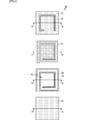
- FIG. 1 is an exploded perspective view showing the main configuration of the multilayer substrate according to the first embodiment of the present invention.
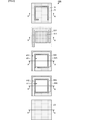
- FIG. 2 is an exploded plan view showing the main configuration of the multilayer substrate according to the first embodiment of the present invention.
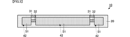
- FIG. 3 is a cross-sectional view showing the main configuration of the multilayer substrate according to the first embodiment of the present invention.
- the multilayer substrate 10 includes a laminated body 20.
- the laminate 20 includes a plurality of resin layers 21, 22, and 23.
- a thickness adjusting member 51 is disposed inside the stacked body 20.
- Each of the plurality of resin layers 21, 22, 23 and the thickness adjusting member 51 is made of a thermoplastic resin and is made of the same material.
- the plurality of resin layers 21, 22, 23 and the thickness adjusting member 51 are made of a material mainly composed of a liquid crystal polymer.
- the plurality of resin layers 21, 22, and 23 have a first main surface and a second main surface that face each other.
- the plurality of resin layers 21, 22, and 23 are stacked.
- the second main surface of the resin layer 21 is in contact with the first main surface of the resin layer 22, and the second main surface of the resin layer 22 is in contact with the first main surface of the resin layer 23.
- the first main surface of the resin layer 21 is the surface of the stacked body 20, and the second main surface of the resin layer 23 is the back surface of the stacked body 20.
- the laminate 20 is realized by disposing a thickness adjusting member 51 in a through hole 42 of the resin layer 22 to be described later, laminating a plurality of resin layers 21, 22, 23, and heating and pressing them.
- the resin layer 22 corresponds to the “first resin layer” of the present invention.
- the resin layer 21 corresponds to the “third resin layer” of the present invention.
- a conductor pattern 31 is formed on the first main surface of the resin layer 21 (the surface of the laminate 20).
- the conductor pattern 31 is linear and has a partially cut annular shape.
- the conductor pattern 31 corresponds to the “surface conductor pattern” of the present invention.
- a conductor pattern 32 is formed on the first main surface of the resin layer 22.
- the conductor pattern 32 is linear and has a partially cut annular shape.
- the conductor pattern 32 overlaps the conductor pattern 31 over substantially the entire length in the linear extending direction in the state of the multilayer body 20.
- the conductor pattern 32 corresponds to the “first inner conductor pattern” of the present invention.
- the resin layer 22 has a through hole 42 that penetrates the resin layer 22 in the thickness direction.
- the through hole 42 is formed in a portion different from the portion where the conductor pattern 32 is formed in the resin layer 22. More specifically, when the resin layer 22 is seen in a plan view, the through hole 42 is composed of a portion that is inside the ring by the conductor pattern 32 and a portion that extends along the conductor pattern 32. Thereby, the through hole 42 is formed so as to be adjacent to the entire length along the direction in which the conductor pattern 32 extends.
- the through hole 42 corresponds to the “through hole for eliminating a level difference” of the present invention.
- the thickness adjusting member 51 is disposed inside the through hole 42. Therefore, in the stacking direction of the stacked body 20 (when the stacked body 20 is viewed from the side), the thickness adjusting member 51 is disposed at a position straddling the conductor pattern 32 and the resin layer 22.
- the shape of the thickness adjusting member 51 in plan view is the same as or substantially the same as the shape of the through hole 42.
- the thickness adjusting member 51 has a thickness that exceeds the length of the through hole 42 in the penetrating direction, that is, the thickness of the resin layer 22.
- the thickness adjusting member 51 is disposed at a position straddling the resin layer 22 and the conductor pattern 32 in the stacking direction.
- the thickness adjusting member 51 has the same length as the sum of the length of the through hole 42 in the penetrating direction (that is, the thickness of the resin layer 22) and the thickness of the conductor pattern 32.
- the length in the penetration direction of the through hole 42 (that is, the thickness of the resin layer 22), the thickness of the conductor pattern 32, and the thickness of the conductor pattern 31 may be the same. Therefore, even if hot pressing is performed, the movement of the conductor pattern 31 and the conductor pattern 32 due to the flow of the resin layers 21 and 22 is suppressed, and the position between the conductor pattern 31 and the conductor pattern 32 as shown in FIG. Deviation is suppressed.
- the conductor pattern 32 has the thickness adjusting member 51 disposed at the same position in the stacking direction, and the thickness adjusting member 51 is disposed so as to straddle the resin layer 22 and the conductor pattern 32 in the stacking direction. . Therefore, both the conductor pattern 32 and the resin layer 22 are in contact with the thickness adjusting member 51 in the side surface direction orthogonal to the stacking direction of the stacked body 20. For this reason, since the same stress is applied to the conductor pattern 32 and the resin layer 22 from the side surface direction during the heating press, the movement of the conductor pattern 32 with respect to the resin layer 22 due to the flow of the resin is more reliably suppressed, and the conductor with respect to the resin layer 22 The positional deviation of the pattern 32 is suppressed.
- the interlayer connection conductor 61 has a shape extending in the stacking direction of the plurality of resin layers 21, 22, and 23 and is a conductor pattern that connects the conductor pattern 31 and the conductor pattern 32.
- the linear conductor patterns 31 and 32 are easy to move in the width direction (direction orthogonal to the extending direction).
- the through hole 42 and the thickness adjusting member 51 of the present embodiment are adjacent to each other over substantially the entire length along the direction in which the conductor patterns 31 and 32 are extended. Thereby, the movement of the conductor patterns 31 and 32 is suppressed over substantially the entire length, and the displacement of the conductor patterns 31 and 32 is suppressed over the substantially entire length. Thereby, the change of the characteristic of the coil which consists of the conductor pattern 31, the conductor pattern 32, and the interlayer connection conductor 61 can be suppressed more reliably.
- the thickness of the thickness adjusting member 51 is such that the thickness of the resin layer 22 after the heat pressing at the portion where the conductor pattern 31 and the conductor pattern 32 overlap in the plan view of the multilayer substrate 10, the conductor The thickness of the pattern 32 and the thickness obtained by adding the thickness of the conductor pattern 31 are substantially the same. That is, in the laminate 20, the through hole 42 is filled with the thickness adjusting member 51. Therefore, as shown in FIG. 3, the thickness of the portion where the conductor pattern 31 and the conductor pattern 32 overlap in the multilayer substrate 10 is the same as the thickness of the portion different from the conductor pattern 31 and the conductor pattern 32 in the multilayer substrate 10.
- the thickness adjusting member 51 before the heating press has the following shape.
- the outer shape in plan view of the thickness adjusting member 51 before the heating press is substantially the same as the shape of the through hole 42 before the heating press, and is smaller than the shape of the through hole 42 before the heating press. Thereby, the thickness adjusting member 51 can be easily disposed inside the through hole 42.
- the thickness of the thickness adjusting member 51 before the heat press exceeds the thickness of the resin layer 22 before the heat press, and preferably the thickness of the resin layer 22 before the heat press, the thickness of the conductor pattern 32, and the conductor pattern 31. It is the thickness which added the thickness of. Thereby, a part of the thickness adjusting member 51 (a portion protruding in the thickness direction from the through hole 42) flows into the gap when the thickness adjusting member 51 in the through hole 42 is disposed, and this flowing portion causes The gap between the through holes 42 is filled. Thereby, the through hole 42 is filled with the thickness adjusting member 51 while suppressing the unevenness of the multilayer substrate 10, and the positional deviation between the conductor pattern 31 and the conductor pattern 32 is suppressed.
- the thickness of the thickness adjusting member 51 before the heat press may be slightly larger than the thickness obtained by adding the thickness of the resin layer 22 before the heat press, the thickness of the conductor pattern 32, and the thickness of the conductor pattern 31.
- the conductor pattern 32 in the multilayer body 20 is more susceptible to the flow of the resin layer than the conductor pattern 31 on the surface of the multilayer body 20. Therefore, at least the movement of the conductor pattern 32 may be suppressed. In this case, the thickness of the thickness adjusting member 51 before the heat press only needs to exceed the thickness of the resin layer 22 before the heat press.
- the conductor pattern 31 is entirely embedded in the laminate 20, but the conductor pattern 31 has a portion in the thickness direction protruding from the surface of the laminate 20. The whole 31 may protrude from the surface of the laminate 20.
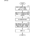
- FIG. 4 is a flowchart showing a first method for manufacturing a multilayer substrate according to an embodiment of the present invention.
- a copper foil patterning process is performed using a photolithographic technique etc. with respect to the some single-sided copper-clad resin sheet in which the copper foil was affixed on the single side
- Etching using a laser or the like is performed on the specific resin sheet on which the conductor pattern is formed, that is, the resin sheet on which the resin layer 22 is formed, to form a through hole 42 for eliminating a step (S102).
- the thickness adjusting member 51 is formed using the same material as the resin sheet for forming the resin layers 21, 22, and 23 (S103).
- the thickness adjusting member 51 is obtained, for example, by etching a portion other than the thickness adjusting member 51 with a laser or the like in a region having the same area as the resin layers 21, 22, and 23 of a flat resin sheet. Alternatively, portions other than the thickness adjusting member 51 may be punched by punching or the like.
- the thickness adjusting member 51 is disposed inside the through hole 42 for level difference elimination, and a plurality of resin sheets for forming the resin layers 21, 22, and 23 are laminated (S104). And this laminated body is heat-pressed (S105). After the heat press, the multilayer substrate 10 is formed by cutting into individual pieces.
- a part of the thickness adjusting member 51 reaches the outer shape of the resin layers 21, 22, and 23 in the flat resin sheet (see the two-dot chain line in FIG. 2). Then, it is preferable. Thereby, when forming the several thickness adjustment member 51 with respect to the sheet of one sheet, the several thickness adjustment member 51 can be connected, and manufacture of the multilayer board
- the manufacturing method of the interlayer connection conductor is not described.
- the through hole for the interlayer connection conductor is formed in the same process as the process of forming the through hole 42 for eliminating the step. Form. Then, after filling the conductive paste in the through hole of the interlayer connection conductor, the step S104 described above may be performed.
- FIG. 5 is an exploded perspective view showing the main configuration of the multilayer board according to the second embodiment of the present invention.
- FIG. 6 is an exploded plan view showing the main configuration of the multilayer substrate according to the second embodiment of the present invention.
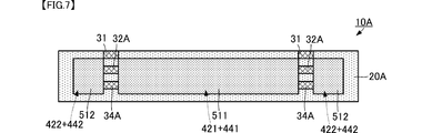
- FIG. 7 is a cross-sectional view showing the main configuration of the multilayer substrate according to the second embodiment of the present invention.
- the multilayer substrate 10A according to the present embodiment is different from the multilayer body 10 of the multilayer substrate 10 according to the first embodiment in that a resin layer 24A is added. Accordingly, the shapes of the resin layer 22A and the thickness adjusting members 511 and 512 are also different from those of the multilayer substrate 10A according to the first embodiment.
- the multilayer substrate 10A includes a laminate 20A.
- the laminated body 20A includes resin layers 21, 22A, 23, and 24A. Thickness adjusting members 511 and 512 are disposed inside the stacked body 20A.
- the resin layers 21, 22A, 23, 24A and the thickness adjusting members 511, 512 are made of the same material.
- the resin layer 22A corresponds to the “first resin layer” of the present invention.
- the resin layer 24A corresponds to the “second resin layer” of the present invention.
- the resin layer 21 corresponds to the “third resin layer” of the present invention.
- the laminated body 20A is laminated in the order of the resin layer 21, the resin layer 22A, the resin layer 24A, and the resin layer 23 from the surface side.
- the resin layers 21 and 23 are the same as the multilayer substrate 10 according to the first embodiment.
- a conductive pattern 32A is formed on the first main surface of the resin layer 22A.
- the conductor pattern 32A is linear and has a partially cut annular shape.
- the conductor pattern 32A overlaps the conductor pattern 31 over substantially the entire length in the linear extending direction in the state of the stacked body 20A.
- the conductor pattern 32A corresponds to the “first inner conductor pattern” of the present invention.
- Through holes 421 and 422 are formed in the resin layer 22A.
- the through hole 421 is inside the ring formed by the conductor pattern 32A when the resin layer 22A is viewed in plan.
- the through-holes 422 are outside the conductor pattern 32A when the resin layer 22A is viewed in plan.
- a conductor pattern 34A is formed on the first main surface of the resin layer 24A.
- the conductor pattern 34A is linear and has a partially cut annular shape.
- the conductor pattern 34A overlaps the conductor pattern 31 and the conductor pattern 32A over substantially the entire length in the linear extending direction in the state of the stacked body 20A.
- the conductor pattern 34A corresponds to the “second inner conductor pattern” of the present invention.
- Through holes 441 and 442 are formed in the resin layer 24A.
- the through hole 441 is inside the ring formed by the conductor pattern 34A when the resin layer 24A is viewed in plan.
- the shape of the through hole 441 in plan view is substantially the same as that of the through hole 421.
- the through hole 441 communicates with the through hole 421 in the state of the stacked body 20A.
- the through-holes 442 are located outside the conductor pattern 34A when the resin layer 24A is viewed in plan.
- the through hole 442 has substantially the same shape as the through hole 422 in a plan view.
- the through hole 442 communicates with the through hole 422 in the state of the stacked body 20A.
- the thickness adjusting member 511 is disposed inside the through holes 421 and 441. Therefore, in the stacking direction of the stacked body 20A (as viewed from the side of the stacked body 20A), the thickness adjusting member 511 is disposed at a position straddling the resin layers 22A and 24A and the conductor patterns 32A and 34A.
- the shape of the thickness adjusting member 511 in a plan view when heated and pressed is the same as the shape of the through holes 421 and 441.
- the thickness adjusting member 512 is disposed inside the through holes 422 and 442. Therefore, in the stacking direction of the stacked body 20A (as viewed from the side of the stacked body 20A), the thickness adjusting member 512 is disposed at a position straddling the resin layers 22A and 24A and the conductor patterns 32A and 34A. In the heated and pressed state, the shape of the thickness adjusting member 512 in plan view is the same as the shape of the through holes 422 and 442.
- the thickness of the thickness adjusting members 511 and 512 before the hot press exceeds the thickness of the resin layer 22A before the hot press and the thickness of the resin layer 24A before the hot press, and preferably the resin before the hot press. This is a thickness obtained by adding the thickness of the layer 22A, the thickness of the resin layer 24A before the heat press, the thickness of the conductor pattern 32A, and the thickness of the conductor pattern 34A.
- the thicknesses of the thickness adjusting members 511 and 512 before the hot press are the thickness of the resin layer 22A before the hot press, the thickness of the resin layer 24A before the hot press, the thickness of the conductor pattern 32A, and the thickness of the conductor pattern 34A. It may be slightly larger than the added thickness.
- the conductor patterns 32A and 34A and the resin layers 22A and 24A are in contact with the thickness adjusting members 511 and 512 in the side surface direction orthogonal to the stacking direction of the stacked body 20A. For this reason, since the same stress is applied to the conductor patterns 32A, 34A and the resin layers 22A, 24A from the side surface direction during the heat press, movement of the conductor patterns 32A, 34A with respect to the resin layers 22A, 24A due to the flow of the resin is suppressed, The positional deviation of the conductor patterns 32A and 34A with respect to the resin layers 22A and 24A is suppressed.
- the thickness adjusting members 511 and 512 straddle the conductor patterns 32A and 34A and the resin layers 22A and 24A, the members straddling the resin layer 22A and the conductor pattern 32A, and the resin layer 24A and the conductor pattern 34A. There is no positional deviation between these members, and the positional deviation of the conductor patterns 32A and 34A with respect to the resin layers 22A and 24A is more reliably suppressed than when the members are straddled.
- the interlayer connection conductors 61A and 62A have a shape extending in the stacking direction of the plurality of resin layers 21, 22A, 24A, and 23.
- the interlayer connection conductor 61A is a conductor pattern that connects the conductor pattern 31 and the conductor pattern 32A.
- the interlayer connection conductor 62A is a conductor pattern that connects the conductor pattern 32A and the conductor pattern 34A.
- the thickness adjusting member is formed from a flat plate made of the same material as the resin layer.
- a resin slurry may be used as the thickness adjusting member.
- FIG. 8 is a flowchart showing a second method for manufacturing a multilayer substrate according to the embodiment of the present invention. Below, the manufacturing method of the multilayer substrate 10 which concerns on 1st Embodiment is shown.
- Step S101 and step S102 are the same as the manufacturing method shown in FIG.
- Resin slurry is filled in the through holes 42 for level difference elimination, and a plurality of resin sheets that respectively form the resin layers 21, 22, and 23 are stacked (S111). At this time, the thickness of the resin slurry is set in the same manner as the thickness of the flat plate thickness adjusting member. And this laminated body is heat-pressed (S105). The resin slurry is solidified by heating at the time of this hot pressing and functions as a thickness adjusting member. After the heat press, the multilayer substrate 10 is formed by cutting into individual pieces.
Landscapes
- Engineering & Computer Science (AREA)
- Power Engineering (AREA)
- Manufacturing & Machinery (AREA)
- Microelectronics & Electronic Packaging (AREA)
- Physics & Mathematics (AREA)
- Optics & Photonics (AREA)
- Production Of Multi-Layered Print Wiring Board (AREA)
- Coils Or Transformers For Communication (AREA)
Abstract
熱可塑性樹脂からなる樹脂層を積層した多層基板における内部の導体パターンの位置ズレを抑制する。多層基板(10)は、積層体(20)、導体パターン(32)、段差解消用の貫通孔(42)、および、厚み調整部材(51)を備える。積層体(20)は、それぞれに熱可塑性樹脂からなる複数の樹脂層(21-23)が積層されてなる。導体パターン(32)は、樹脂層(22)の主面に形成され、且つ積層体(20)の内部に配置されている。段差解消用の貫通孔(42)は、積層体(20)を平面視して導体パターン(32)と異なる位置にあり、樹脂層(22)を厚み方向に貫通する。厚み調整部材(51)は、樹脂層(21-23)と同じ材質からなり、貫通孔(42)の内部に配置され、樹脂層(22)の厚みを超える厚みを有する。
Description
本発明は、複数の樹脂層を積層した積層体からなり、該積層体内に導体パターンを有する多層基板に関する。
多層基板の一種として、特許文献1には、多層アンテナが記載されている。特許文献1の多層アンテナは、それぞれにアンテナ用の導体パターンが形成された複数の樹脂シートと、導体パターンが形成されていない緩衝シートとを積層してなる。緩衝シートには、スリットが形成されている。
これら複数の樹脂シートと緩衝シートとを積層する際、積層した状態を平面視して、導体パターンとスリットとが重なるように配置される。これにより、導体パターンがスリットに埋まるように積層され、積層方向に並ぶ導体パターン間の位置ズレが抑制される。
しかしながら、上述の特許文献1に示す樹脂シートおよび緩衝シートが熱可塑性樹脂である場合、複数の樹脂シートと緩衝シートとを積層状態において加熱プレスする。このような加熱プレスを行うと、緩衝シートの流動が生じ、緩衝シートの流動によって、導体パターンとスリットとの位置関係がずれてしまうことがある。この場合、導体パターンの位置ズレが生じてしまう可能性がある。
したがって、本発明の目的は、それぞれが熱可塑性樹脂からなる複数の樹脂層を積層してなり、内部に導体パターンを有する多層基板において、内部の導体パターンの位置ズレを抑制することにある。
この発明の多層基板は、積層体、第1の内部導体パターン、段差解消用の貫通孔、および、厚み調整部材を備える。積層体は、それぞれに熱可塑性樹脂からなる複数の樹脂層が積層されてなる。第1の内部導体パターンは、複数の樹脂層に含まれる第1の樹脂層の主面に形成され、且つ積層体の内部に配置されている。段差解消用の貫通孔は、積層体を平面視して第1の内部導体パターンと異なる位置にあり、第1の樹脂層を厚み方向に貫通する。厚み調整部材は、複数の樹脂層と同じ材質からなり、貫通孔の内部に配置され、第1の樹脂層の厚みを超える厚みを有する。
この構成では、導体パターンが形成されていない部分に形成された段差解消用の貫通孔と厚み調整部材とによって、導体パターンが形成されていない部分の厚みが調整され、導体パターンを有する部分との厚みの差が緩和される。
また、この発明の多層基板では、厚み調整部材は、複数の樹脂層の積層方向において、第1の樹脂層と第1の内部導体パターンとに跨って配置されていることが好ましい。
この構成では、第1の内部導体パターンと第1の樹脂層とがともに、積層体の積層方向と直交する側面方向で、厚み調整部材と接する。このため、加熱プレス時に側面方向から第1の内部導体パターンと第1の樹脂層とに同様の応力が加わるので、第1の樹脂層に対する第1の内部導体パターンの位置ズレが生じ難い。
また、この発明の多層基板では、厚み調整部材は、複数の樹脂層と同じ熱可塑性樹脂からなることが好ましい。
この構成では、厚み調整部材と複数の樹脂層との加熱プレス時における状態が同じになる。これにより、厚みの差の緩和効果が向上する。
また、この発明の多層基板では、厚み調整部材の厚みは、第1の樹脂層の厚みと第1の内部導体パターンの厚みとを加算した厚みと同じであることが好ましい。
この構成では、厚みの差がさらに確実に小さくなる。
また、この発明の多層基板は、次の構成であってもよい。多層基板は、複数の樹脂層に含まれる第2の樹脂層の主面に形成され、且つ積層体の内部に配置された第2の内部導体パターンを、さらに備える。第2の樹脂層は、積層方向において第1の樹脂層に隣接している。第2の内部導体パターンは、積層体を平面視して、第1の内部導体パターンに重なる部分を有している。段差解消用の貫通孔は、積層体を平面視して第2の内部導体パターンと異なる位置にあり、第1の樹脂層と第2の樹脂層とを貫通している。厚み調整部材は、第1の樹脂層の厚み、および、第2の樹脂層の厚みを超える厚みを有する。
この構成では、積層体内に積層方向に並んで、第1の内部導体パターンが配置される第1の樹脂層と、第2の内部導体パターンが配置される第2の樹脂層とがあり、第1の樹脂層と第2の樹脂層を跨るように、1つの厚み調整部材が配置される。これにより、それぞれに複数の厚み調整部材を用いる場合と比較して、厚み調整部材間の位置ズレに伴う第1の内部導体パターンと第2の内部導体パターンとの間の位置ズレが抑制される。
また、この発明の多層基板では、厚み調整部材の厚みは、第1の樹脂層の厚み、第1の内部導体パターンの厚み、第2の樹脂層の厚み、および第2の内部導体パターンの厚みを加算した厚みと同じであることが好ましい。
この構成では、第1の樹脂層、第2の樹脂層、第1の内部導体パターン、および、第2の内部導体パターンを跨るように、1つの厚み調整部材が配置される。これにより、第1の内部導体パターンと第2の内部導体パターンとの間の位置ズレがさらに確実に抑制される。
また、この発明の多層基板は、第1の内部導体パターンと第2の内部導体パターンとは線状導体であり、積層方向に延びる層間接続導体で接続されていてもよい。
この構成では、例えば、第1の内部導体パターンと第2の内部導体パターンとを含むコイルが形成される。そして、コイルとして用いる場合、第1の内部導体パターンと第2の内部導体パターンとの間の位置ズレが抑制されることで、コイルの特性が安定または向上する。
また、この発明の多層基板では、次の構成であってもよい。多層基板は、積層体の表面を形成する第3の樹脂層の表面に形成された表面導体パターンを備える。表面導体パターンは、積層体を平面視して、第1の内部導体パターンに重なる部分を有している。厚み調整部材は、第1の樹脂層の厚みを超える厚みを有する。
この構成では、積層方向に並ぶ第1の内部導体パターンと表面導体パターンがあり、これら第1の内部導体パターンと表面導体パターンとの間の位置ズレが抑制される。
また、この発明の多層基板では、厚み調整部材の厚みは、第1の樹脂層の厚み、第1の内部導体パターンの厚み、および表面導体パターンの厚みを加算した厚みと同じであることが好ましい。
この構成では、第1の内部導体パターンと表面導体パターンとの間の位置ズレがさらに確実に抑制される。
また、この発明の多層基板では、第1の内部導体パターンと表面導体パターンとは、線状導体であり、積層方向に延びる層間接続導体で接続されていてもよい。
この構成では、例えば、第1の内部導体パターンと表面導体パターンとを含むコイルが形成される。そして、コイルとして用いる場合、第1の内部導体パターンと表面導体パターンとの位置ズレが抑制されることで、コイルの特性が安定または向上する。
また、この発明の多層基板の製造方法では、次の各工程を有する。多層基板の製造方法は、熱可塑性樹脂からなる第1の樹脂層の主面に内部導体パターンを形成する。多層基板の製造方法は、第1の樹脂層における内部導体パターンと異なる位置に、第1の樹脂層を厚み方向に貫通する段差解消用の貫通孔を形成する。多層基板の製造方法は、厚み調整部材を形成する。厚み調整部材は、段差解消用の貫通孔に嵌る形状であり、第1の樹脂層と同じ材質からなり、第1の樹脂層の厚みと内部導体パターンの厚みとを加算した厚みを少なくとも有する。多層基板の製造方法は、内部導体パターンが積層体の内部に配置されるように第1の樹脂層を含むそれぞれが熱可塑性樹脂からなる複数の樹脂層を積層して積層体を形成する。多層基板の製造方法は、積層体を加熱プレスする。
この製造方法では、加熱プレス前に、段差解消用の貫通孔内に厚み調整部材が配置される。したがって、加熱プレス時に段差解消用の貫通孔と厚み調整部材との間の位置ズレは生じず、第1の内部導体パターンの位置ズレが抑制される。
また、この発明の多層基板の製造方法では、次の各工程を有する。多層基板の製造方法は、熱可塑性樹脂からなる第1の樹脂層の主面に内部導体パターンを形成する。多層基板の製造方法は、第1の樹脂層における内部導体パターンと異なる位置に、第1の樹脂層を厚み方向に貫通する段差解消用の貫通孔を形成する。多層基板の製造方法は、内部導体パターンが積層体の内部に配置されるように第1の樹脂層を含むそれぞれが熱可塑性樹脂からなる複数の樹脂層を積層し、段差解消用の貫通孔に樹脂スラリーを充填して、積層体を形成する。多層基板の製造方法は、積層体を加熱プレスする。
この製造方法では、加熱プレス前に、段差解消用の貫通孔内に樹脂スラリーが充填される。したがって、内部導体パターンの位置ズレが抑制される。
この発明によれば、それぞれが熱可塑性樹脂からなる複数の樹脂層を積層してなり、内部に導体パターンを有する多層基板において、内部の導体パターンの位置ズレを抑制できる。
本発明の第1の実施形態に係る多層基板について、図を参照して説明する。図1は、本発明の第1の実施形態に係る多層基板の主要構成を示す分解斜視図である。図2は、本発明の第1の実施形態に係る多層基板の主要構成を示す分解平面図である。図3は、本発明の第1の実施形態に係る多層基板の主要構成を示す断面図である。
図1、図2、図3に示すように、多層基板10は、積層体20を備える。積層体20は、複数の樹脂層21、22、23を備える。積層体20の内部には厚み調整部材51が配置されている。複数の樹脂層21、22、23、および、厚み調整部材51は、それぞれが熱可塑性樹脂からなり、同じ材質からなる。例えば、複数の樹脂層21、22、23、および、厚み調整部材51は、液晶ポリマを主成分とする材質からなる。
複数の樹脂層21、22、23は、それぞれに対向する第1主面と第2主面を有する。複数の樹脂層21、22、23は、積層されている。樹脂層21の第2主面は、樹脂層22の第1主面に当接し、樹脂層22の第2主面は樹脂層23の第1主面に当接している。樹脂層21の第1主面は、積層体20の表面であり、樹脂層23の第2主面は、積層体20の裏面である。
積層体20は、後述する樹脂層22の貫通孔42内に厚み調整部材51を配置して、複数の樹脂層21、22、23を積層し、これらを加熱プレスすることによって実現される。樹脂層22が、本発明の「第1の樹脂層」に対応する。樹脂層21が、本発明の「第3の樹脂層」に対応する。
樹脂層21の第1主面(積層体20の表面)には、導体パターン31が形成されている。導体パターン31は、線状であり、部分的に切れた環状である。導体パターン31が、本発明の「表面導体パターン」に対応する。
樹脂層22の第1主面には、導体パターン32が形成されている。導体パターン32は、線状であり、部分的に切れた環状である。導体パターン32は、積層体20の状態において、線状の延びる方向の略全長に亘って、導体パターン31に重なっている。導体パターン32が、本発明の「第1の内部導体パターン」に対応する。
樹脂層22には、樹脂層22を厚み方向に貫通する貫通孔42が形成されている。貫通孔42は、樹脂層22における導体パターン32が形成されている部分とは異なる部分に形成されている。より具体的には、樹脂層22を平面視して、貫通孔42は、導体パターン32による環の内側になる部分と、導体パターン32に沿って延びる部分とからなる。これにより、貫通孔42は、導体パターン32を延びる方向に沿って略全長に亘って隣接するように形成されている。この貫通孔42が、本発明の「段差解消用の貫通孔」に対応する。
厚み調整部材51は、貫通孔42の内部に配置されている。したがって、積層体20の積層方向において(積層体20を側面視して)、厚み調整部材51は、導体パターン32および樹脂層22に跨る位置に配置されている。
加熱プレスされた状態において、厚み調整部材51の平面視した形状は、貫通孔42の形状と同じもしくは実質的に同じである。そして、厚み調整部材51は、貫通孔42の貫通方向の長さ、すなわち、樹脂層22の厚みを超える厚みとなる。言い換えれば、厚み調整部材51は、樹脂層22と導体パターン32とに積層方向に跨った位置に配置されている。好ましくは、厚み調整部材51は、貫通孔42の貫通方向の長さ(すなわち樹脂層22の厚み)と導体パターン32の厚みとを加算した長さと同じである。また、貫通孔42の貫通方向の長さ(すなわち樹脂層22の厚み)と導体パターン32の厚みと導体パターン31の厚みとを加算した長さと同じにしていてもよい。したがって、加熱プレスを行っても、樹脂層21、22の流動による導体パターン31および導体パターン32の移動が抑制され、図3に示すように、導体パターン31と導体パターン32との間での位置ズレが抑制される。
特に、導体パターン32は、積層方向の同じ位置に厚み調整部材51が配置されており、且つ、厚み調整部材51は、樹脂層22と導体パターン32とに積層方向に跨るように配置されている。したがって、導体パターン32と樹脂層22とがともに、積層体20の積層方向と直交する側面方向で、厚み調整部材51と接する。このため、加熱プレス時に側面方向から導体パターン32と樹脂層22とに同様の応力が加わるので、樹脂の流動による樹脂層22に対する導体パターン32の移動はより確実に抑制され、樹脂層22に対する導体パターン32の位置ズレが抑制される。
これにより、図1に示すように、導体パターン31、導体パターン32、および、層間接続導体61によってスパイラル形状のコイルを形成する場合、当該コイルの特性の変化を抑制できる。なお、層間接続導体61は、複数の樹脂層21、22、23の積層方向に延びる形状であり、導体パターン31と導体パターン32とを接続する導体パターンである。
特に、線状の導体パターン31、32は、幅方向(延びる方向に直交する方向)に移動しやすい。しかしながら、本実施形態の貫通孔42と厚み調整部材51とは、導体パターン31、32を延びる方向に沿って略全長に亘って隣接している。これにより、導体パターン31、32の移動が略全長に亘って抑制され、導体パターン31、32の移動が略全長に亘って位置ズレが抑制される。これにより、導体パターン31、導体パターン32、および、層間接続導体61からなるコイルの特性の変化をより確実に抑制できる。
また、加熱プレスされた状態において、厚み調整部材51の厚みは、多層基板10を平面視して導体パターン31と導体パターン32とが重なっている部分における加熱プレス後の樹脂層22の厚み、導体パターン32の厚み、および、導体パターン31の厚みを加算した厚みと略同じである。すなわち、積層体20では、貫通孔42が厚み調整部材51によって埋められている。したがって、図3に示すように、多層基板10における導体パターン31と導体パターン32とが重なる部分の厚みと、多層基板10における導体パターン31と導体パターン32と異なる部分の厚みとが同じになる。
このような形状を容易に且つ確実に実現するため、加熱プレス前の厚み調整部材51は、次の形状であることが好ましい。
加熱プレス前の厚み調整部材51の平面視の外形は、加熱プレス前の貫通孔42の形状と略同じであり、且つ、加熱プレス前の貫通孔42の形状よりも小さい。これにより、厚み調整部材51を貫通孔42の内部に容易に配置できる。
加熱プレス前の厚み調整部材51の厚みは、加熱プレス前の樹脂層22の厚みを超えており、好ましくは、加熱プレス前の樹脂層22の厚み、導体パターン32の厚み、および、導体パターン31の厚みを加算した厚みである。これにより、貫通孔42内の厚み調整部材51が配置される際の隙間に、加熱プレス時に厚み調整部材51の一部(貫通孔42から厚み方向に突出する部分)が流れ込み、この流れ込む部分によって貫通孔42の隙間が埋められる。これにより、多層基板10の凹凸を抑制しながら、貫通孔42が厚み調整部材51によって充填され、導体パターン31と導体パターン32との間での位置ズレが抑制される。なお、加熱プレス前の厚み調整部材51の厚みは、加熱プレス前の樹脂層22の厚み、導体パターン32の厚み、および、導体パターン31の厚みを加算した厚みよりもやや大きくてもよい。
なお、積層体20の内部にある導体パターン32は、積層体20の表面にある導体パターン31よりも樹脂層の流動の影響を受けやすい。したがって、少なくとも導体パターン32の移動を抑制すればよい。この場合、加熱プレス前の厚み調整部材51の厚みは、加熱プレス前の樹脂層22の厚みを超えていればよい。
また、上述の図3に示す態様では、導体パターン31は、積層体20に全体が埋まっているが、導体パターン31の厚み方向の一部が積層体20の表面から突出している態様、導体パターン31の全体が積層体20の表面から突出している態様であってもよい。
このような構成からなる多層基板10は、次に示す製造方法によって製造される。図4は、本発明の実施形態に係る多層基板の第1の製造方法を示すフローチャートである。
熱可塑性樹脂からなる基材の片面に銅箔が貼り付けられた複数の片面銅貼り樹脂シートに対して、フォトリソグラフィ技術等を用いて、銅箔のパターニング処理を行う(S101)。これにより、樹脂層21の導体パターン31および樹脂層22の導体パターン32を形成する。
導体パターンが形成された特定の樹脂シート、すなわち樹脂層22を形成する樹脂シートに、レーザ等を用いたエッチングを行い、段差解消用の貫通孔42を形成する(S102)。
樹脂層21、22、23を形成する樹脂シートと同じ材質を用いて、厚み調整部材51を形成する(S103)。厚み調整部材51は、例えば、平板の樹脂シートの樹脂層21、22、23と同じ面積の領域において、厚み調整部材51以外の部分をレーザ等によってエッチングすることで得られる。あるいは、厚み調整部材51以外の部分をパンチング等によって型抜きしてもよい。
厚み調整部材51を段差解消用の貫通孔42の内部に配置し、樹脂層21、22、23をそれぞれに形成する複数の樹脂シートを積層する(S104)。そして、この積層体を加熱プレスする(S105)。加熱プレス後は、それぞれ個片に切り分け、多層基板10を形成する。
このような製造方法を用いることによって、導体パターンの位置ズレが抑制された多層基板を容易に製造することができる。
また、上述の製造方法では、図2に示すように、厚み調整部材51の一部が、平板の樹脂シートにおける樹脂層21、22、23の外形(図2の二点鎖線を参照)に達するとことが好ましい。これにより、一枚の樹脂シートに対して複数の厚み調整部材51を形成する場合に、複数の厚み調整部材51を繋げることができ、マルチ状での多層基板10の製造が容易になる。
なお、上述の説明では、層間接続導体の製造方法を記載していないが、概略的には、段差解消用の貫通孔42を形成する工程と同様の工程で、層間接続導体用の貫通孔を形成する。そして、層間接続導体の貫通孔の導電ペーストを充填した後に、上述のステップS104の工程を行えばよい。
次に、本発明の第2の実施形態に係る多層基板について、図を参照して説明する。図5は、本発明の第2の実施形態に係る多層基板の主要構成を示す分解斜視図である。図6は、本発明の第2の実施形態に係る多層基板の主要構成を示す分解平面図である。図7は、本発明の第2の実施形態に係る多層基板の主要構成を示す断面図である。
本実施形態に係る多層基板10Aは、第1の実施形態に係る多層基板10の積層体20に対して、樹脂層24Aが追加された点で異なる。これに伴い、樹脂層22Aおよび厚み調整部材511、512の形状も第1の実施形態に係る多層基板10Aと異なる。
図5、図6、図7に示すように、多層基板10Aは、積層体20Aを備える。積層体20Aは、樹脂層21、22A、23、24Aを備える。積層体20Aの内部には、厚み調整部材511、512が配置されている。樹脂層21、22A、23、24Aと厚み調整部材511、512とは同じ材質からなる。樹脂層22Aが、本発明の「第1の樹脂層」に対応する。樹脂層24Aが、本発明の「第2の樹脂層」に対応する。樹脂層21が、本発明の「第3の樹脂層」に対応する。
積層体20Aは、表面側から樹脂層21、樹脂層22A、樹脂層24A、樹脂層23の順で積層されている。樹脂層21、23は、第1の実施形態に係る多層基板10と同じである。
樹脂層22Aの第1主面には、導体パターン32Aが形成されている。導体パターン32Aは、線状であり、部分的に切れた環状である。導体パターン32Aは、積層体20Aの状態において、線状の延びる方向の略全長に亘って、導体パターン31に重なっている。導体パターン32Aが、本発明の「第1の内部導体パターン」に対応する。
樹脂層22Aには、貫通孔421、422が形成されている。貫通孔421は、樹脂層22Aを平面視して、導体パターン32Aによる環の内側にある。貫通孔422は、樹脂層22Aを平面視して、導体パターン32Aによる間の外側にある。
樹脂層24Aの第1主面には、導体パターン34Aが形成されている。導体パターン34Aは、線状であり、部分的に切れた環状である。導体パターン34Aは、積層体20Aの状態において、線状の延びる方向の略全長に亘って、導体パターン31および導体パターン32Aに重なっている。導体パターン34Aが、本発明の「第2の内部導体パターン」に対応する。
樹脂層24Aには、貫通孔441、442が形成されている。貫通孔441は、樹脂層24Aを平面視して、導体パターン34Aによる環の内側にある。貫通孔441は、平面視の形状が、貫通孔421と略同じである。貫通孔441は、積層体20Aの状態で、貫通孔421と連通している。
貫通孔442は、樹脂層24Aを平面視して、導体パターン34Aによる間の外側にある。貫通孔442は、平面視の形状が、貫通孔422と略同じである。貫通孔442は、積層体20Aの状態で、貫通孔422と連通している。
厚み調整部材511は、貫通孔421、441の内部に配置されている。したがって、積層体20Aの積層方向において(積層体20Aを側面視して)、厚み調整部材511は、樹脂層22A、24Aおよび導体パターン32A、34Aに跨る位置に配置されている。加熱プレスされた状態において、厚み調整部材511の平面視した形状は、貫通孔421、441の形状と同じである。
厚み調整部材512は、貫通孔422、442の内部に配置されている。したがって、積層体20Aの積層方向において(積層体20Aを側面視して)、厚み調整部材512は、樹脂層22A、24Aおよび導体パターン32A、34Aに跨る位置に配置されている。加熱プレスされた状態において、厚み調整部材512の平面視した形状は、貫通孔422、442の形状と同じである。
加熱プレス前の厚み調整部材511、512の厚みは、加熱プレス前の樹脂層22Aの厚みと加熱プレス前の樹脂層24Aの厚みを加算した厚みを超えており、好ましくは、加熱プレス前の樹脂層22Aの厚み、加熱プレス前の樹脂層24Aの厚み、導体パターン32Aの厚み、および、導体パターン34Aの厚みを加算した厚みである。なお、加熱プレス前の厚み調整部材511、512の厚みは、加熱プレス前の樹脂層22Aの厚み、加熱プレス前の樹脂層24Aの厚み、導体パターン32Aの厚み、および、導体パターン34Aの厚みを加算した厚みよりもやや大きくてもよい。
この構成により、第1の実施形態と同様に、導体パターン32A、34Aと樹脂層22A、24Aとがともに、積層体20Aの積層方向と直交する側面方向で、厚み調整部材511、512と接する。このため、加熱プレス時に側面方向から導体パターン32A、34Aと樹脂層22A、24Aとに同様の応力が加わるので、樹脂の流動による樹脂層22A、24Aに対する導体パターン32A、34Aの移動は抑制され、樹脂層22A、24Aに対する導体パターン32A、34Aの位置ズレが抑制される。すなわち、積層体20Aの内部に、二層の導体パターンが形成されていても、これらの導体パターンの位置ズレを抑制することができる。なお、導体パターンが三層以上であっても、同様の構成を適用することによって、位置ズレを抑制できる。また、厚み調整部材511、512は、導体パターン32A、34Aと樹脂層22A、24Aとに跨っているので、樹脂層22Aと導体パターン32Aとに跨る部材と、樹脂層24Aと導体パターン34Aとに跨る部材とから構成するよりも、これらの部材間の位置ズレもなく、樹脂層22A、24Aに対する導体パターン32A、34Aの位置ズレがより確実に抑制される。
これにより、図5に示すように、導体パターン31、導体パターン32A、導体パターン34A、および、層間接続導体61A、61Bによってスパイラル形状のコイルを形成する場合、当該コイルの特性の変化を抑制できる。なお、層間接続導体61A、62Aは、複数の樹脂層21、22A、24A、23の積層方向に延びる形状である。層間接続導体61Aは、導体パターン31と導体パターン32Aとを接続する導体パターンである。層間接続導体62Aは、導体パターン32Aと導体パターン34Aとを接続する導体パターンである。
なお、上述の説明では、樹脂層と同じ材質の平板から厚み調整部材を形成する態様を示したが、厚み調整部材として、樹脂スラリーを用いてもよい。図8は、本発明の実施形態に係る多層基板の第2の製造方法を示すフローチャートである。以下では、第1の実施形態に係る多層基板10の製造方法を示している。
ステップS101およびステップS102は、図4に示す製造方法と同じであり、説明を省略する。
樹脂スラリーを段差解消用の貫通孔42内に充填して、樹脂層21、22、23をそれぞれに形成する複数の樹脂シートを積層する(S111)。この際、樹脂スラリーの厚みは、上述の平板の厚み調整部材の厚みと同じように設定されている。そして、この積層体を加熱プレスする(S105)。この加熱プレス時の加熱によって、樹脂スラリーが固化して、厚み調整部材として機能する。加熱プレス後は、それぞれ個片に切り分け、多層基板10を形成する。
このような製造方法を用いても、導体パターンの位置ズレが抑制された多層基板を容易に製造することができる。
10、10A:多層基板
20、20A:積層体
21、22、22A、23、24A:樹脂層
31、32、32A、34A:導体パターン
42、421、422、441、442:貫通孔
51、511、512:厚み調整部材
61、61A、62A:層間接続導体
20、20A:積層体
21、22、22A、23、24A:樹脂層
31、32、32A、34A:導体パターン
42、421、422、441、442:貫通孔
51、511、512:厚み調整部材
61、61A、62A:層間接続導体
Claims (13)
- それぞれに熱可塑性樹脂からなる複数の樹脂層が積層された積層体と、
前記複数の樹脂層に含まれる第1の樹脂層の主面に形成され、且つ前記積層体の内部に配置された第1の内部導体パターンと、
前記積層体を平面視して前記第1の内部導体パターンと異なる位置にあり、前記第1の樹脂層を厚み方向に貫通する段差解消用の貫通孔と、
前記複数の樹脂層と同じ材質からなり、前記貫通孔の内部に配置され、前記第1の樹脂層の厚みを超える厚みを有する厚み調整部材と、
を備える、多層基板。 - 前記厚み調整部材は、前記複数の樹脂層の積層方向において、前記第1の樹脂層と前記第1の内部導体パターンとに跨って配置されている、
請求項1に記載の多層基板。 - 前記厚み調整部材は、前記複数の樹脂層と同じ熱可塑性樹脂からなる、
請求項1または請求項2に記載の多層基板。 - 前記厚み調整部材の厚みは、前記第1の樹脂層の厚みと前記第1の内部導体パターンの厚みとを加算した厚みと同じである、
請求項1乃至請求項3のいずれかに記載の多層基板。 - 前記複数の樹脂層に含まれる第2の樹脂層の主面に形成され、且つ前記積層体の内部に配置された第2の内部導体パターンを、さらに備え、
前記第2の樹脂層は、積層方向において前記第1の樹脂層に隣接しており、
前記第2の内部導体パターンは、前記積層体を平面視して、前記第1の内部導体パターンに重なる部分を有しており、
前記段差解消用の貫通孔は、前記積層体を平面視して前記第2の内部導体パターンと異なる位置にあり、前記第1の樹脂層と前記第2の樹脂層とを貫通しており、
前記厚み調整部材は、
前記第1の樹脂層の厚み、および、前記第2の樹脂層の厚みを加算した厚みを超える厚みを有する、
請求項1乃至請求項4のいずれかに記載の多層基板。 - 前記厚み調整部材の厚みは、前記第1の樹脂層の厚み、前記第1の内部導体パターンの厚み、前記第2の樹脂層の厚み、および前記第2の内部導体パターンの厚みを加算した厚みと同じである、
請求項5に記載の多層基板。 - 前記第1の内部導体パターンと前記第2の内部導体パターンとは、線状の導体であり、前記積層方向に延びる層間接続導体で接続されている、
請求項5または請求項6に記載の多層基板。 - 前記積層体の表面を形成する第3の樹脂層の表面に形成された表面導体パターンを備え、
前記表面導体パターンは、前記積層体を平面視して、前記第1の内部導体パターンに重なる部分を有しており、
前記厚み調整部材は、
前記第1の樹脂層の厚みを超える厚みを有する、
請求項1乃至請求項3のいずれかに記載の多層基板。 - 前記厚み調整部材の厚みは、前記第1の樹脂層の厚み、前記第1の内部導体パターンの厚み、および前記表面導体パターンの厚みを加算した厚みと同じである、
請求項8に記載の多層基板。 - 前記第1の内部導体パターンと前記表面導体パターンとは、線状の導体であり、前記複数の樹脂層の積層方向に延びる層間接続導体で接続されている、
請求項8または請求項9に記載の多層基板。 - 熱可塑性樹脂からなる第1の樹脂層の主面に内部導体パターンを形成する工程と、
前記第1の樹脂層における前記内部導体パターンと異なる位置に、前記第1の樹脂層を厚み方向に貫通する段差解消用の貫通孔を形成する工程と、
前記段差解消用の貫通孔に嵌る形状であり、前記第1の樹脂層と同じ材質からなり、前記第1の樹脂層の厚みを超える厚みを有する厚み調整部材を形成する工程と、
前記内部導体パターンが積層体の内部に配置されるように前記第1の樹脂層を含むそれぞれが熱可塑性樹脂からなる複数の樹脂層を積層して前記積層体を形成する工程と、
前記積層体を加熱プレスする工程と、
を有する多層基板の製造方法。 - 前記厚み調整部材の厚みは、前記第1の樹脂層の厚みと前記内部導体パターンの厚みとを加算した厚みと同じである、
請求項11に記載の多層基板の製造方法。 - 熱可塑性樹脂からなる第1の樹脂層の主面に内部導体パターンを形成する工程と、
前記第1の樹脂層における前記内部導体パターンと異なる位置に、前記第1の樹脂層を厚み方向に貫通する段差解消用の貫通孔を形成する工程と、
前記内部導体パターンが積層体の内部に配置されるように前記第1の樹脂層を含むそれぞれが熱可塑性樹脂からなる複数の樹脂層を積層し、前記段差解消用の貫通孔に樹脂スラリーを充填して、前記積層体を形成する工程と、
前記積層体を加熱プレスする工程と、
を有する多層基板の製造方法。
Priority Applications (3)
| Application Number | Priority Date | Filing Date | Title |
|---|---|---|---|
| CN201780030176.3A CN109156082B (zh) | 2016-05-18 | 2017-05-11 | 多层基板以及多层基板的制造方法 |
| JP2017554417A JP6372624B2 (ja) | 2016-05-18 | 2017-05-11 | 多層基板、および、多層基板の製造方法 |
| US16/166,194 US11443886B2 (en) | 2016-05-18 | 2018-10-22 | Multilayer substrate and method of producing multilayer substrate |
Applications Claiming Priority (2)
| Application Number | Priority Date | Filing Date | Title |
|---|---|---|---|
| JP2016099451 | 2016-05-18 | ||
| JP2016-099451 | 2016-05-18 |
Related Child Applications (1)
| Application Number | Title | Priority Date | Filing Date |
|---|---|---|---|
| US16/166,194 Continuation US11443886B2 (en) | 2016-05-18 | 2018-10-22 | Multilayer substrate and method of producing multilayer substrate |
Publications (1)
| Publication Number | Publication Date |
|---|---|
| WO2017199826A1 true WO2017199826A1 (ja) | 2017-11-23 |
Family
ID=60325982
Family Applications (1)
| Application Number | Title | Priority Date | Filing Date |
|---|---|---|---|
| PCT/JP2017/017775 Ceased WO2017199826A1 (ja) | 2016-05-18 | 2017-05-11 | 多層基板、および、多層基板の製造方法 |
Country Status (4)
| Country | Link |
|---|---|
| US (1) | US11443886B2 (ja) |
| JP (1) | JP6372624B2 (ja) |
| CN (1) | CN109156082B (ja) |
| WO (1) | WO2017199826A1 (ja) |
Cited By (1)
| Publication number | Priority date | Publication date | Assignee | Title |
|---|---|---|---|---|
| US20220141965A1 (en) * | 2019-08-08 | 2022-05-05 | Murata Manufacturing Co., Ltd. | Multilayer substrate and method of manufacturing multilayer substrate |
Citations (3)
| Publication number | Priority date | Publication date | Assignee | Title |
|---|---|---|---|---|
| JPH04321295A (ja) * | 1991-02-28 | 1992-11-11 | Toppan Printing Co Ltd | プリント配線板の製造方法 |
| JP2012099600A (ja) * | 2010-11-01 | 2012-05-24 | Kyocera Corp | 積層型電子部品の製造方法 |
| WO2015129601A1 (ja) * | 2014-02-27 | 2015-09-03 | 株式会社村田製作所 | 電磁石の製造方法、および、電磁石 |
Family Cites Families (5)
| Publication number | Priority date | Publication date | Assignee | Title |
|---|---|---|---|---|
| JP2944308B2 (ja) * | 1991-11-08 | 1999-09-06 | 三菱電機株式会社 | 多層プリント基板の製法 |
| JP3407737B2 (ja) * | 2000-12-14 | 2003-05-19 | 株式会社デンソー | 多層基板の製造方法およびその製造方法によって形成される多層基板 |
| JP5077800B2 (ja) * | 2005-10-11 | 2012-11-21 | 住友電気工業株式会社 | 多層プリント配線板の製造方法 |
| JP5636842B2 (ja) * | 2010-09-24 | 2014-12-10 | 株式会社村田製作所 | 多層アンテナの製造方法 |
| CN103329637B (zh) * | 2011-02-08 | 2016-04-13 | 株式会社村田制作所 | 树脂多层基板及其制造方法 |
-
2017
- 2017-05-11 WO PCT/JP2017/017775 patent/WO2017199826A1/ja not_active Ceased
- 2017-05-11 CN CN201780030176.3A patent/CN109156082B/zh active Active
- 2017-05-11 JP JP2017554417A patent/JP6372624B2/ja active Active
-
2018
- 2018-10-22 US US16/166,194 patent/US11443886B2/en active Active
Patent Citations (3)
| Publication number | Priority date | Publication date | Assignee | Title |
|---|---|---|---|---|
| JPH04321295A (ja) * | 1991-02-28 | 1992-11-11 | Toppan Printing Co Ltd | プリント配線板の製造方法 |
| JP2012099600A (ja) * | 2010-11-01 | 2012-05-24 | Kyocera Corp | 積層型電子部品の製造方法 |
| WO2015129601A1 (ja) * | 2014-02-27 | 2015-09-03 | 株式会社村田製作所 | 電磁石の製造方法、および、電磁石 |
Cited By (2)
| Publication number | Priority date | Publication date | Assignee | Title |
|---|---|---|---|---|
| US20220141965A1 (en) * | 2019-08-08 | 2022-05-05 | Murata Manufacturing Co., Ltd. | Multilayer substrate and method of manufacturing multilayer substrate |
| US12563677B2 (en) * | 2019-08-08 | 2026-02-24 | Murata Manufacturing Co., Ltd. | Multilayer substrate and method of manufacturing multilayer substrate |
Also Published As
| Publication number | Publication date |
|---|---|
| US11443886B2 (en) | 2022-09-13 |
| CN109156082B (zh) | 2021-02-09 |
| US20190057802A1 (en) | 2019-02-21 |
| CN109156082A (zh) | 2019-01-04 |
| JP6372624B2 (ja) | 2018-08-15 |
| JPWO2017199826A1 (ja) | 2018-06-07 |
Similar Documents
| Publication | Publication Date | Title |
|---|---|---|
| US9485860B2 (en) | Multilayer board | |
| EP2467004B1 (en) | Manufacturing method of multilayer substrate and multilayer substrate produced by the manufacturing method | |
| JP6424453B2 (ja) | 多層基板の製造方法および多層基板 | |
| WO2015079941A1 (ja) | 多層基板の製造方法、多層基板および電磁石 | |
| US11923123B2 (en) | Multilayer substrate and a manufacturing method of the multilayer substrate | |
| JP6536695B2 (ja) | 積層型コイル | |
| US10709020B2 (en) | Component-embedded substrate and method for manufacturing component-embedded substrate | |
| US11523521B2 (en) | Multilayer board and method of manufacturing the same | |
| US20130220691A1 (en) | Multilayer wiring substrate and method of manufacturing the same | |
| JP6372624B2 (ja) | 多層基板、および、多層基板の製造方法 | |
| CN207124812U (zh) | 线圈内置基板 | |
| JP6263167B2 (ja) | 多層基板および多層基板の製造方法 | |
| JP6536751B2 (ja) | 積層コイルおよびその製造方法 | |
| JP6562076B2 (ja) | 樹脂基板、部品搭載樹脂基板およびその製造方法 | |
| CN204425772U (zh) | 多层基板 | |
| JP2012186451A5 (ja) | ||
| WO2019026835A1 (ja) | 多層プリント配線板の製造方法及び多層プリント配線板 | |
| WO2017026208A1 (ja) | 樹脂多層基板およびその製造方法 | |
| JP2015050422A (ja) | 樹脂多層基板およびその製造方法 | |
| WO2017159437A1 (ja) | 回路基板およびその製造方法 | |
| WO2021067129A1 (en) | Dual conductor laminated substrate | |
| CN208258200U (zh) | 树脂多层基板 | |
| JP2015046498A (ja) | 多層プリント基板およびその製造方法 | |
| JPWO2021025073A5 (ja) | 伝送線路の製造方法及び伝送線路 | |
| JP2000106486A (ja) | 多層配線板の製造方法 |
Legal Events
| Date | Code | Title | Description |
|---|---|---|---|
| ENP | Entry into the national phase |
Ref document number: 2017554417 Country of ref document: JP Kind code of ref document: A |
|
| NENP | Non-entry into the national phase |
Ref country code: DE |
|
| 121 | Ep: the epo has been informed by wipo that ep was designated in this application |
Ref document number: 17799250 Country of ref document: EP Kind code of ref document: A1 |
|
| 122 | Ep: pct application non-entry in european phase |
Ref document number: 17799250 Country of ref document: EP Kind code of ref document: A1 |