WO2017199734A1 - 積層フィルタ - Google Patents
積層フィルタ Download PDFInfo
- Publication number
- WO2017199734A1 WO2017199734A1 PCT/JP2017/016981 JP2017016981W WO2017199734A1 WO 2017199734 A1 WO2017199734 A1 WO 2017199734A1 JP 2017016981 W JP2017016981 W JP 2017016981W WO 2017199734 A1 WO2017199734 A1 WO 2017199734A1
- Authority
- WO
- WIPO (PCT)
- Prior art keywords
- inductor
- capacitor
- layer
- electrode
- pass filter
- Prior art date
- Legal status (The legal status is an assumption and is not a legal conclusion. Google has not performed a legal analysis and makes no representation as to the accuracy of the status listed.)
- Ceased
Links
Images





Classifications
-
- H—ELECTRICITY
- H01—ELECTRIC ELEMENTS
- H01F—MAGNETS; INDUCTANCES; TRANSFORMERS; SELECTION OF MATERIALS FOR THEIR MAGNETIC PROPERTIES
- H01F17/00—Fixed inductances of the signal type
-
- H—ELECTRICITY
- H01—ELECTRIC ELEMENTS
- H01F—MAGNETS; INDUCTANCES; TRANSFORMERS; SELECTION OF MATERIALS FOR THEIR MAGNETIC PROPERTIES
- H01F27/00—Details of transformers or inductances, in general
-
- H—ELECTRICITY
- H01—ELECTRIC ELEMENTS
- H01F—MAGNETS; INDUCTANCES; TRANSFORMERS; SELECTION OF MATERIALS FOR THEIR MAGNETIC PROPERTIES
- H01F27/00—Details of transformers or inductances, in general
- H01F27/28—Coils; Windings; Conductive connections
- H01F27/29—Terminals; Tapping arrangements for signal inductances
-
- H—ELECTRICITY
- H03—ELECTRONIC CIRCUITRY
- H03H—IMPEDANCE NETWORKS, e.g. RESONANT CIRCUITS; RESONATORS
- H03H7/00—Multiple-port networks comprising only passive electrical elements as network components
- H03H7/01—Frequency selective two-port networks
-
- H—ELECTRICITY
- H03—ELECTRONIC CIRCUITRY
- H03H—IMPEDANCE NETWORKS, e.g. RESONANT CIRCUITS; RESONATORS
- H03H7/00—Multiple-port networks comprising only passive electrical elements as network components
- H03H7/01—Frequency selective two-port networks
- H03H7/075—Ladder networks, e.g. electric wave filters
Definitions
- the present invention relates to a multilayer filter including an LC resonator.
- Patent Document 1 discloses a multilayer low-pass filter including an LC parallel resonator and an LC series resonator.
- the output terminal of the first inductor is connected to the input terminal of the second inductor.
- the first capacitor is connected in parallel to the first inductor.
- the second capacitor is connected in parallel to the second inductor.
- the third capacitor connects the output terminal of the first inductor and the input terminal of the second inductor to the ground conductor layer.
- the fourth capacitor connects the input end of the first inductor and the ground conductor layer.
- the fifth capacitor connects the output terminal of the second inductor and the ground conductor layer.
- the conductive portion having an inductance component connects the ground conductor layer and the ground terminal.
- the multilayer low-pass filter disclosed in Japanese Patent Laying-Open No. 2009-182376 has first and second inductors included in the LC parallel resonator and an inductance component included in the LC series resonator.
- the dielectric layer on which the conductive portion is formed is close to one side of the laminated structure.
- the dielectric layers on which the first and second capacitors included in the LC parallel resonator and the third to fifth capacitors included in the LC series resonator are formed depend on the other side of the multilayer structure. Therefore, the first inductor, the second inductor, and the conductive portion are arranged close to each other and are magnetically coupled.
- mutual inductance may occur between the respective inductors.
- the difference between the characteristics of the low-pass filter assumed from the circuit diagram designed to obtain the desired characteristics and the characteristics of the low-pass filter consisting of the actual laminated structure may be larger than expected.
- an additional inductor or capacitor is required, for example, to ensure impedance matching or attenuation.
- the size of the multilayer low-pass filter may increase, or the manufacturing cost may increase.
- the present invention has been made to solve the above-described problems, and its purpose is to deviate the characteristics of the multilayer filter from the desired characteristics while suppressing an increase in the size of the multilayer filter and an increase in manufacturing cost. Is to suppress this.
- a multilayer filter is a multilayer filter formed of a plurality of dielectric layers.
- the multilayer filter includes an LC parallel resonator and an LC series resonator.
- the LC parallel resonator includes a first inductor and a first capacitor.
- the LC series resonator includes a second inductor and a second capacitor.
- the plurality of dielectric layers include a first inductor layer, a second inductor layer, and a capacitor layer. In the first inductor layer, the first inductor is formed.
- the second inductor layer is formed with a second inductor.
- the capacitor layer includes a capacitor layer in which a first capacitor and a second capacitor are formed. The capacitor layer is disposed between the first inductor layer and the second inductor layer.
- the multilayer filter of the present invention by disposing the capacitor layer between the first inductor layer and the second inductor layer and separating the first inductor layer and the second inductor layer, the two are magnetically coupled. Suppress. As a result, it is possible to suppress a deviation from specific desired characteristics of the multilayer filter while suppressing an increase in the size of the multilayer filter and an increase in manufacturing cost.
- FIG. 3 is a circuit diagram of a low-pass filter that is an example of the multilayer filter according to Embodiment 1.
- FIG. It is an external appearance perspective view of the low pass filter of FIG. It is a disassembled perspective view which shows the laminated structure of the low pass filter of FIG. It is a figure which shows the positional relationship of each layer when the low-pass filter shown by FIG. 3 is seen from the side. It is a figure which shows the simulation result of the attenuation
- damping characteristic of the low-pass filter shown by FIG. 6 is an exploded perspective view showing a laminated structure of a low-pass filter that is an example of a laminated filter according to Embodiment 2.
- FIG. 7 is a diagram illustrating a perspective view of the low-pass filter shown in FIG. 3 and the low-pass filter shown in FIG. It is a figure which shows the simulation result of the attenuation characteristic of the low pass filter shown by FIG.
- FIG. 1 is a circuit diagram of a low-pass filter 1 that is an example of the multilayer filter according to the first embodiment.
- the low-pass filter 1 includes an input / output terminal P1, which is a first terminal, an input / output terminal P2, which is a second terminal, an LC parallel resonator LC1, and an LC series resonator LC2. .
- LC parallel resonator LC1 includes a first inductor L1 and a first capacitor C1.
- the first inductor L1 is connected between the input / output terminal P1 and the input / output terminal P2.
- the first capacitor C1 is connected in parallel to the first inductor L1 between the input / output terminal P1 and the input / output terminal P2.
- LC series resonator LC2 includes a second inductor L2, a second capacitor C2, and a third capacitor C3.
- the second inductor is connected to the ground electrode GND whose one end is a ground point.
- the second capacitor C2 is connected between the input / output terminal P1 and the other end of the second inductor L2.
- the third capacitor C3 is connected between the input / output terminal P2 and the other end of the second inductor L2.
- the number of sets of inductors and capacitors in the low-pass filter 1 is one in the LC parallel resonator LC1 (first inductor L1 and first capacitor C1), and two in the LC series resonator LC2 (second inductor L2 and A second capacitor C2, and a second inductor L2 and a third capacitor C3). That is, the low pass filter 1 is a third order low pass filter. When comparing the low-pass filter 1 and the third-order low-pass filter with respect to the insertion loss, the power loss is reduced by the smaller number of inductors or capacitors through which the signal passes. small.
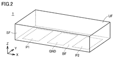
- FIG. 2 is an external perspective view of the low-pass filter 1 of FIG.
- the low-pass filter 1 has a rectangular parallelepiped shape, for example.
- surfaces perpendicular to the stacking direction are defined as a bottom surface BF and a top surface UF.
- Input / output terminals P1 and P2 and a ground electrode GND are formed on the bottom surface BF.
- the input / output terminals P1 and P2 and the ground electrode GND are, for example, LGA (Land Grid Array) terminals in which planar electrodes are arranged in a grid pattern on the bottom surface BF.
- LGA Land Grid Array
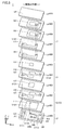
- FIG. 3 is an exploded perspective view showing a laminated structure of the low-pass filter 1 of FIG.
- the low-pass filter 1 is a multilayer filter formed from a plurality of dielectric layers.
- the low-pass filter 1 includes dielectric layers Lyr100 to Lyr110 as a plurality of dielectric layers. The layers are stacked in the Z-axis direction in this order, with Lyr100 as the bottom surface BF side and Lyr110 as the top surface UF side.
- Line electrodes 101 to 103 are formed on the dielectric layer Lyr100.
- the line electrode 101 is connected to the input / output terminal P1 by the via electrode V111.
- the line electrode 102 is connected to the ground electrode GND by a via electrode V112.
- the line electrode 103 is connected to the input / output terminal P2 by the via electrode V113.
- the line electrode 102 forms a second inductor L2.
- the dielectric layer Lyr100 corresponds to the second inductor layer of the present invention.
- a capacitor electrode 111 is formed on the dielectric layer Lyr101.
- the capacitor electrode 111 is connected to the line electrode 102 by a via electrode V121.
- Capacitor electrodes 121 and 122 are formed on the dielectric layer Lyr102.
- the capacitor electrode 121 is connected to the line electrode 101 by a via electrode V131.
- the capacitor electrode 122 is connected to the line electrode 103 by a via electrode V132.
- Capacitor electrodes 111 and 121 form a second capacitor C2.
- Capacitor electrodes 111 and 122 form a third capacitor C3.
- a capacitor electrode 131 is formed on the dielectric layer Lyr103.
- Capacitor electrodes 141 and 142 are formed on the dielectric layer Lyr104.
- the capacitor electrode 141 is connected to the capacitor electrode 121 by a via electrode V131.
- the capacitor electrode 142 is connected to the capacitor electrode 122 by a via electrode V132.
- a capacitor electrode 151 is formed on the dielectric layer Lyr105. Capacitor electrodes 131, 141, 142, and 151 form a first capacitor C1.
- the dielectric layers Lyr101 to Lyr105 correspond to the capacitor layer of the present invention.
- a line electrode 161 is formed on the dielectric layer Lyr106. The line electrode 161 is connected to the capacitor electrode 141 by the via electrode V131.
- a line electrode 171 is formed on the dielectric layer Lyr107. The line electrode 171 is connected to the line electrode 161 by via electrodes V131 and V141.
- a line electrode 181 is formed on the dielectric layer Lyr108. The line electrode 181 is connected to the line electrode 171 by a via electrode V141. The line electrode 181 is connected to the capacitor electrode 142 by the via electrode V132.
- a line electrode 191 is formed on the dielectric layer Lyr109. The line electrode 191 is connected to the line electrode 181 by via electrodes V141 and V132.
- the line electrodes 161, 171, 181, and 191 form a first inductor L1.
- the dielectric layers Lyr106 to Lyr109 correspond to the first inductor layer of the present invention.
- the line electrodes 161 and 171 included in the first inductor L1 have the same shape and substantially overlap in the stacking direction. The same applies to the line electrodes 181 and 191 included in the first inductor L1.
- the volume (or cross-sectional area) through which current flows increases.
- the magnetic flux generated from the first inductor L1 is increased, and the effective inductance of the LC parallel resonator is improved.
- the Q value of the low-pass filter 1 can be improved.
- first inductor L1 and the second inductor L2 are formed in adjacent dielectric layers, they are magnetically coupled to each other, and there is a possibility that mutual inductance occurs in addition to the inductance of the first inductor L1 and the inductance of the second inductor L2. is there. Therefore, it is assumed that there is a divergence between the characteristics assumed from the circuit diagram of the low-pass filter 1 shown in FIG. 1 designed to obtain a desired characteristic and the characteristics of the low-pass filter 1 having the laminated structure shown in FIG. Can be larger. In that case, for example, an additional inductor or capacitor is required to ensure impedance matching or attenuation. As a result, there is a possibility that the size of the low-pass filter 1 becomes large or the manufacturing cost increases.
- the capacitor layer is disposed between the first inductor layer and the second inductor layer.
- the first inductor layer and the second inductor layer can be separated. Therefore, magnetic coupling between the first inductor formed in the first inductor layer and the second inductor formed in the second inductor layer can be suppressed. As a result, it is possible to prevent a characteristic such as characteristic impedance or attenuation characteristic from deviating from a desired characteristic without adding an inductor or a coil.
- FIG. 4 is a diagram showing the positional relationship of each layer when the low-pass filter 1 shown in FIG. 3 is viewed from the side surface SF.
- the capacitor layer (the layer in which the first capacitor C1, the second capacitor C2, and the third capacitor C3 are formed) is the first inductor layer (the layer in which the first inductor L1 is formed).
- the second inductor layer (the layer in which the second inductor L2 is formed).
- FIG. 5 is a diagram showing a simulation result of the attenuation characteristic of the low-pass filter 1 shown in FIG.
- the frequency Fc1 is a cut-off frequency at which the attenuation (dB) decreases by a predetermined value (for example, 3 dB).
- Point AP11 represents the attenuation pole of the LC parallel resonator LC1.
- Point AP12 represents the attenuation pole of the LC series resonator LC2. As shown in FIG.
- an attenuation of about ⁇ 38 dB is realized at the attenuation pole AP11 (around 5.2 GHz), and an attenuation of about ⁇ 32 dB at the attenuation pole AP12 (around 5.8 GHz). The amount is realized.
- the capacitor layer is disposed between the first inductor layer and the second inductor layer, and the first inductor layer and the second inductor layer are separated from each other, whereby both are magnetic. Suppresses binding. As a result, it is possible to suppress the characteristics of the multilayer filter from deviating from desired characteristics while suppressing an increase in the size of the multilayer filter and an increase in manufacturing cost.
- the distance D11 between the first inductor layer and the capacitor layer is larger than the distance D12 between the second inductor layer and the capacitor layer. Even when the distance D11 is smaller than the distance D12, it is possible to suppress the characteristics of the multilayer filter from deviating from desired characteristics while suppressing an increase in the size of the multilayer filter and an increase in manufacturing cost.
- the Q value of the LC resonator increases as the effective inductance of the inductor included in the LC resonator increases, and decreases as the resistance component of the inductor increases.
- the effective inductance of the first inductor L1 decreases.
- the resistance component of the first inductor L1 hardly changes. Therefore, when the magnetic flux generated in the first inductor L1 is obstructed by an electrode such as a capacitor electrode included in the capacitor layer, the Q value of the LC1 of the first LC parallel resonator is lowered.
- the magnetic flux generated by the first inductor L1 is applied to the capacitor layer as in the first embodiment.
- the attenuation amount of the LC series resonator LC2 is brought close to the attenuation pole of the LC parallel resonator LC1 to realize the attenuation amount.
- it is necessary to balance both the Q values so that one of the Q values does not deteriorate too much.
- the distance between the first inductor layer and the capacitor layer is substantially equal to the distance between the second inductor layer and the capacitor layer.
- the Q value of the LC parallel resonator LC1 and the Q value of the LC series resonator LC2 can be balanced.
- a desired attenuation desired to be realized by the low-pass filter can be ensured.
- substantially equal is not only the case where the two are completely coincident with each other, but the error from the distance when they are completely equal is, for example, due to accuracy problems in manufacturing or manufacturing variations. This includes cases where there is a degree.
- FIGS. 3, 4, and 5 of the first embodiment are replaced with FIGS. 6, 7, and 9 of the second embodiment, respectively. Since other configurations are the same, the description will not be repeated.
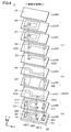
- FIG. 6 is an exploded perspective view showing a laminated structure of the low-pass filter 2 which is an example of the laminated filter according to the second embodiment.
- the low-pass filter 2 is a multilayer filter formed from a plurality of dielectric layers.
- the low-pass filter 2 includes dielectric layers Lyr200 to Lyr209 as a plurality of dielectric layers. The layers are stacked in the Z-axis direction in this order, with Lyr 200 as the bottom surface BF side and Lyr 209 as the top surface UF side.
- Line electrodes 201 to 203 are formed on the dielectric layer Lyr200.
- the line electrode 201 is connected to the input / output terminal P1 by the via electrode V211.
- the line electrode 202 is connected to the ground electrode GND by a via electrode V212.
- the line electrode 203 is connected to the input / output terminal P2 by the via electrode V213.
- Line electrodes 211 to 213 are formed on the dielectric layer Lyr201.
- the line electrode 211 is connected to the line electrode 201 by via electrodes V211 and V221.
- the line electrode 212 is connected to the line electrode 202 by via electrodes V212 and V222.
- the line electrode 213 is connected to the line electrode 203 by via electrodes V213 and V223.
- the line electrodes 202 and 212 form a second inductor L2. Dielectric layers Lyr200 and 201 correspond to the second inductor layer of the present invention.
- a capacitor electrode 221 is formed on the dielectric layer Lyr202.
- the capacitor electrode 221 is connected to the line electrode 212 by a via electrode V222.
- Capacitor electrodes 231 and 232 are formed on the dielectric layer Lyr203.
- the capacitor electrode 231 is connected to the line electrode 211 by a via electrode V221.
- the capacitor electrode 232 is connected to the line electrode 213 by a via electrode V223.
- Capacitor electrodes 221 and 231 form a second capacitor C2.
- Capacitor electrodes 221 and 232 form a third capacitor C3.
- a capacitor electrode 241 is formed on the dielectric layer Lyr204.
- the capacitor electrodes 231, 232, and 241 form a first capacitor C1.
- the dielectric layers Lyr202 to Lyr204 correspond to the capacitor layer of the present invention.
- the Lyr 202 to Lyr 204 are preferably fired (co-fire) simultaneously with the capacitor electrodes 221, 231, 232, and 241.
- the dielectric constant of the capacitor layer can be increased, and the capacitor layer can be made thinner. it can.
- the distance between the first inductor layer and the capacitor layer and the distance between the second inductor layer and the capacitor layer can be further increased.
- a line electrode 251 is formed on the dielectric layer Lyr205.
- the line electrode 251 is connected to the capacitor electrode 232 by the via electrode V223.
- a line electrode 261 is formed on the dielectric layer Lyr206.
- the line electrode 261 is connected to the line electrode 251 by via electrodes V231 and V223.
- a line electrode 271 is formed on the dielectric layer Lyr207.
- the line electrode 271 is connected to the capacitor electrode 231 by the via electrode V221.
- the line electrode 271 is connected to the line electrode 261 by a via electrode V231.
- a line electrode 281 is formed on the dielectric layer Lyr208.
- the line electrode 281 is connected to the line electrode 271 by via electrodes V221 and V231.
- the line electrodes 251, 261, 271, and 281 form the first inductor L 1.
- the dielectric layers Lyr205 to Lyr208 correspond to the first inductor layer of the present invention.
- the line electrodes 251 and 261 included in the first inductor L1 have the same shape and substantially overlap in the stacking direction. The same applies to the line electrodes 271 and 281 included in the first inductor L1. The same applies to the line electrodes 202 and 212 included in the second inductor L2.
- the volume (or cross-sectional area) through which current flows increases, the magnetic flux generated from the first inductor L1 increases, and the effective inductance of the LC parallel resonator increases.
- the magnetic flux generated from the second inductor L2 increases, and the effective inductance of the LC series resonator increases.
- the Q value of the low-pass filter 2 can be improved.
- FIG. 7 is a diagram showing the positional relationship of each layer when the low-pass filter 2 shown in FIG. 6 is viewed from the side.
- the capacitor layer (the layer in which the first capacitor C1, the second capacitor C2, and the third capacitor C3 are formed) is the first inductor layer (the layer in which the first inductor L1 is formed).
- the second inductor layer (the layer in which the second inductor L2 is formed).
- the distance D21 between the first inductor layer and the capacitor layer is substantially equal to the distance D22 between the second inductor layer and the capacitor layer.
- the distance D21 between the first inductor layer and the capacitor layer, the distance D22 between the second inductor layer and the capacitor layer, and the distance D23 between the second inductor layer and the ground electrode GND are as follows. Almost equal.
- the distance D23 between the second inductor layer and the ground electrode GND substantially equal to the distances D21 and D22, the second inductor layer and the ground electrode GND can be separated. It is possible to suppress the magnetic flux generated from the second inductor L2 from being hindered by the ground electrode GND, and to suppress heat generation due to the generation of eddy current. As a result, the insertion loss of the low-pass filter 2 can be reduced, and the Q value of the low-pass filter 2 can be further improved.
- the magnetic flux generated from the first inductor L1 is not disturbed by the capacitor electrode included in the capacitor layer as the distance between the first inductor layer and the capacitor layer is increased.
- FIG. 8 is a diagram showing perspective views of the low-pass filter 1 shown in FIG. 3 and the low-pass filter 2 shown in FIG. 6 when viewed from the upper surface UF in the stacking direction.
- the low pass filter 1 which is an example of the multilayer filter according to the first embodiment is included in the plurality of capacitors formed in the capacitor layer in the stacking direction of the plurality of dielectric layers. Capacitor electrodes 111, 131, 141, and 151 almost block the air core portion AC1 of the first inductor L1.
- the low pass filter 2 which is an example of the multilayer filter according to the second embodiment, a plurality of capacitors formed in the capacitor layer in the stacking direction of the plurality of dielectric layers.
- the capacitor formed in the capacitor layer is disposed so as not to block the air core portion AC2 of the first inductor L1.
- the plurality of capacitors formed in the capacitor layer are desirably arranged so as not to overlap with the air core part AC2 of the first inductor L1. The same applies to the air core part of the second inductor L2.
- the magnetic flux generated from the first inductor L1 and the second inductor L2 is not hindered by the capacitor electrodes included in the capacitor layer than in the first embodiment. ing.
- FIG. 9 is a diagram showing a simulation result of the attenuation characteristic of the low-pass filter 2 shown in FIG.
- the frequency Fc2 is a cutoff frequency.
- a point AP21 indicates an attenuation pole due to the LC parallel resonator LC1.
- a point AP22 indicates an attenuation pole due to the LC series resonator LC2.
- an attenuation of about ⁇ 48 dB is realized at the attenuation pole AP21 (near 5.4 GHz), and an attenuation of about ⁇ 46 dB at the attenuation pole AP22 (near 6.1 GHz). The amount is realized.
- the second embodiment realizes a larger attenuation in both the attenuation pole by the LC parallel resonator LC1 and the attenuation pole by the LC series resonator LC2.
- the capacitor layer is disposed between the first inductor layer and the second inductor layer, and the first inductor layer and the second inductor layer are separated from each other, whereby both are magnetic. Suppresses binding. As a result, it is possible to suppress the characteristics of the multilayer filter from deviating from desired characteristics while suppressing an increase in the size of the multilayer filter and an increase in manufacturing cost.
- each of the LC parallel resonator and the LC series resonator is The deterioration of the Q value can be suppressed in a well-balanced manner, and as a result, the Q value of the entire low-pass filter can be improved as compared with the first embodiment. As a result, a desired attenuation can be realized in the multilayer filter according to the second embodiment.
Landscapes
- Engineering & Computer Science (AREA)
- Power Engineering (AREA)
- Microelectronics & Electronic Packaging (AREA)
- Filters And Equalizers (AREA)
Abstract
積層フィルタのサイズの大型化よび製造コストの増加を抑制しながら、積層フィルタの特性が所望の特性から乖離することを抑制する。本発明の一実施形態による積層フィルタ(1)は、LC並列共振器と、LC直列共振器とを備える。LC並列共振器は、第1インダクタ(L1)および第1コンデンサ(C1)を含む。LC直列共振器は、第2インダクタ(L2)および第2コンデンサ(C2)を含む。複数の誘電体層は、第1インダクタ層と、第2インダクタ層と、コンデンサ層とを含む。第1インダクタ層は、第1インダクタ(L1)が形成されている。第2インダクタ層は、第2インダクタ(L2)が形成されている。コンデンサ層は、第1コンデンサ(C1)および第2コンデンサ(C2)が形成されている。コンデンサ層は、第1インダクタ層および第2インダクタ層の間に配置されている。
Description
この発明は、LC共振器を備える積層フィルタに関する。
従来から、LC共振器を備える積層フィルタが知られている。たとえば、特開2009-182376号公報(特許文献1)には、LC並列共振器およびLC直列共振器を備える積層型ローパスフィルタが開示されている。特開2009-182376号公報(特許文献1)のLC並列共振器において、第1のインダクタの出力端は、第2のインダクタの入力端に接続されている。第1のキャパシタは、第1のインダクタに対して並列に接続されている。第2のキャパシタは、第2のインダクタに対して並列に接続されている。直列共振器において、第3のキャパシタは、第1のインダクタの出力端および第2のインダクタの入力端と、グランド用導体層とを接続している。第4のキャパシタは、第1のインダクタの入力端とグランド用導体層とを接続している。第5のキャパシタは、第2のインダクタの出力端とグランド用導体層とを接続している。インダクタンス成分を有する導電部は、グランド用導体層とグランド用端子とを接続している。このような構成により、ローパスフィルタの阻止帯域中に存在する特定の狭い周波数帯域における減衰量を特に大きくすることが可能になる。
特開2009-182376号公報(特許文献1)に開示されている積層型ローパスフィルタにおいて、LC並列共振器に含まれる第1および第2のインダクタ、並びにLC直列共振器に含まれるインダクタンス成分を有する導電部が形成されている誘電体層は積層構造の一方の側に寄っている。一方、LC並列共振器に含まれる第1および第2のキャパシタ、並びにLC直列共振器に含まれる第3~第5のキャパシタが形成されている誘電体層は積層構造の他方の側によっている。そのため、第1のインダクタ、第2のインダクタ、および導電部が近接配置され、それぞれが磁気結合する。その結果、第1のインダクタのインダクタンス、第2のインダクタのインダクタンス、および導電部のインダクタンスに加えて、それぞれのインダクタ間において、相互インダクタンスが生じる可能性がある。相互インダクタンスが生じると、所望の特性が得られるように設計された回路図から想定されるローパスフィルタの特性と、実際の積層構造からなるローパスフィルタの特性との乖離が想定よりも大きくなる可能性がある。特性のずれが大きくなると、たとえばインピーダンス整合あるいは減衰量の確保のために、追加のインダクタあるいはコンデンサが必要になる。その結果、積層型ローパスフィルタのサイズが大きくなったり、製造コストが増加したりするおそれがある。
本発明は上記のような課題を解決するためになされたものであり、その目的は積層フィルタのサイズの大型化よび製造コストの増加を抑制しながら、積層フィルタの特性が所望の特性から乖離するのを抑制することである。
本発明の一実施形態による積層フィルタは、複数の誘電体層から形成された積層フィルタである。積層フィルタは、LC並列共振器と、LC直列共振器とを備える。LC並列共振器は、第1インダクタおよび第1コンデンサを含む。LC直列共振器は、第2インダクタおよび第2コンデンサを含む。複数の誘電体層は、第1インダクタ層と、第2インダクタ層と、コンデンサ層とを含む。第1インダクタ層は、第1インダクタが形成されている。第2インダクタ層は、第2インダクタが形成されている。コンデンサ層は、第1コンデンサおよび第2コンデンサが形成されているコンデンサ層とを含む。コンデンサ層は、第1インダクタ層および第2インダクタ層の間に配置されている。
本発明に係る積層フィルタによれば、コンデンサ層を第1インダクタ層および第2インダクタ層の間に配置して第1インダクタ層と第2インダクタ層とを離すことにより、両者が磁気結合することを抑制する。その結果、積層フィルタのサイズの大型化および製造コストの増加を抑制しながら、積層フィルタの特定の所望の特性からの乖離を抑制することができる。
以下、本発明の実施の形態について、図面を参照しながら詳細に説明する。なお、図中同一または相当部分には同一符号を付してその説明は繰り返さない。
[実施の形態1]
図1は、実施の形態1に係る積層フィルタの一例であるローパスフィルタ1の回路図である。図1に示されるように、ローパスフィルタ1は、第1端子である入出力端子P1と、第2端子である入出力端子P2と、LC並列共振器LC1と、LC直列共振器LC2とを備える。
図1は、実施の形態1に係る積層フィルタの一例であるローパスフィルタ1の回路図である。図1に示されるように、ローパスフィルタ1は、第1端子である入出力端子P1と、第2端子である入出力端子P2と、LC並列共振器LC1と、LC直列共振器LC2とを備える。
LC並列共振器LC1は、第1インダクタL1および第1コンデンサC1を含む。第1インダクタL1は、入出力端子P1および入出力端子P2の間に接続されている。第1コンデンサC1は、入出力端子P1および入出力端子P2の間で第1インダクタL1に対して並列に接続されている。
LC直列共振器LC2は、第2インダクタL2、第2コンデンサC2、および第3コンデンサC3を含む。第2インダクタは、一方端が接地点である接地電極GNDに接続されている。第2コンデンサC2は、入出力端子P1と第2インダクタL2の他方端との間に接続されている。第3コンデンサC3は、入出力端子P2と第2インダクタL2の他方端との間に接続されている。
ローパスフィルタ1におけるインダクタとコンデンサとの組の数は、LC並列共振器LC1において1つ(第1インダクタL1と第1コンデンサC1)であり、LC直列共振器LC2において2つ(第2インダクタL2と第2コンデンサC2、および第2インダクタL2と第3コンデンサC3)である。すなわち、ローパスフィルタ1は3次のローパスフィルタである。挿入損失について、ローパスフィルタ1と3次より大きいローパスフィルタとを比較すると、信号が通過するインダクタあるいはコンデンサの数が少ない分だけ電力の損失が低減されるため、ローパスフィルタ1の挿入損失の方が小さい。
図2は、図1のローパスフィルタ1の外観斜視図である。図2に示されるように、ローパスフィルタ1はたとえば直方体状である。ローパスフィルタ1の面に関して、積層方向に垂直な面を底面BFおよび上面UFとする。底面BFには、入出力端子P1、P2、および接地電極GNDが形成されている。入出力端子P1、P2、および接地電極GNDは、たとえば底面BFに平面電極が格子状に配置されたLGA(Land Grid Array)端子である。
図3は、図1のローパスフィルタ1の積層構造を示す分解斜視図である。ローパスフィルタ1は、複数の誘電体層から形成された積層フィルタである。ローパスフィルタ1は、複数の誘電体層として誘電体層Lyr100~Lyr110を備える。Lyr100を底面BF側、Lyr110を上面UF側として、この順にZ軸方向に積層されている。
誘電体層Lyr100には、線路電極101~103が形成されている。線路電極101はビア電極V111によって入出力端子P1に接続されている。線路電極102はビア電極V112によって接地電極GNDに接続されている。線路電極103はビア電極V113によって入出力端子P2に接続されている。線路電極102は第2インダクタL2を形成している。誘電体層Lyr100は本発明の第2インダクタ層に対応する。
誘電体層Lyr101にはキャパシタ電極111が形成されている。キャパシタ電極111はビア電極V121によって線路電極102に接続されている。誘電体層Lyr102にはキャパシタ電極121および122が形成されている。キャパシタ電極121はビア電極V131によって線路電極101に接続されている。キャパシタ電極122はビア電極V132によって線路電極103に接続されている。キャパシタ電極111および121は第2コンデンサC2を形成している。キャパシタ電極111および122は第3コンデンサC3を形成している。
誘電体層Lyr103にはキャパシタ電極131が形成されている。誘電体層Lyr104にはキャパシタ電極141および142が形成されている。キャパシタ電極141はビア電極V131によってキャパシタ電極121に接続されている。キャパシタ電極142はビア電極V132によってキャパシタ電極122に接続されている。誘電体層Lyr105にはキャパシタ電極151が形成されている。キャパシタ電極131、141、142、および151は第1コンデンサC1を形成している。
誘電体層Lyr101~Lyr105は本発明のコンデンサ層に対応する。
誘電体層Lyr106には線路電極161が形成されている。線路電極161はビア電極V131によってキャパシタ電極141に接続されている。誘電体層Lyr107には線路電極171が形成されている。線路電極171はビア電極V131およびV141によって線路電極161に接続されている。誘電体層Lyr108には線路電極181が形成されている。線路電極181はビア電極V141によって線路電極171に接続されている。線路電極181はビア電極V132によってキャパシタ電極142に接続されている。誘電体層Lyr109には線路電極191が形成されている。線路電極191はビア電極V141およびV132によって線路電極181に接続されている。線路電極161、171、181、および191は第1インダクタL1を形成している。誘電体層Lyr106~Lyr109は本発明の第1インダクタ層に対応する。
誘電体層Lyr106には線路電極161が形成されている。線路電極161はビア電極V131によってキャパシタ電極141に接続されている。誘電体層Lyr107には線路電極171が形成されている。線路電極171はビア電極V131およびV141によって線路電極161に接続されている。誘電体層Lyr108には線路電極181が形成されている。線路電極181はビア電極V141によって線路電極171に接続されている。線路電極181はビア電極V132によってキャパシタ電極142に接続されている。誘電体層Lyr109には線路電極191が形成されている。線路電極191はビア電極V141およびV132によって線路電極181に接続されている。線路電極161、171、181、および191は第1インダクタL1を形成している。誘電体層Lyr106~Lyr109は本発明の第1インダクタ層に対応する。
第1インダクタL1に含まれる線路電極161および171は同形状であり、積層方向において略重なっている。第1インダクタL1に含まれる線路電極181および191についても同様である。このような形状および配置とすることにより、電流が流れる体積(あるいは断面積)が増える。また、第1インダクタL1から発生する磁束が大きくなり、LC並列共振器の実効インダクタンスが向上する。その結果、ローパスフィルタ1のQ値を向上させることができる。
第1インダクタL1および第2インダクタL2を近接する誘電体層に形成した場合、それぞれが磁気結合し、第1インダクタL1のインダクタンスおよび第2インダクタL2のインダクタンスに加えて、相互インダクタンスが生じる可能性がある。そのため、所望の特性が得られるように設計された図1に示されるローパスフィルタ1の回路図から想定される特性と、図3に示される積層構造からなるローパスフィルタ1の特性との乖離が想定よりも大きくなる可能性がある。その場合、たとえばインピーダンス整合あるいは減衰量の確保のために追加のインダクタあるいはコンデンサが必要になる。その結果、ローパスフィルタ1のサイズが大きくなったり、製造コストが増加したりするおそれがある。
そこで実施の形態1では、コンデンサ層を第1インダクタ層および第2インダクタ層の間に配置する。このような構成により、第1インダクタ層および第2インダクタ層を離すことができる。そのため、第1インダクタ層に形成されている第1インダクタおよび第2インダクタ層に形成されている第2インダクタが磁気結合することを抑制することができる。その結果、インダクタあるいはコイルを追加することなく、たとえば特性インピーダンスあるいは減衰特性のような特性が所望の特性から乖離することを抑制することができる。
図4は、図3に示されるローパスフィルタ1を側面SFから見たときの各層の位置関係を示す図である。図4に示されるように、コンデンサ層(第1コンデンサC1、第2コンデンサC2、および第3コンデンサC3が形成されている層)は、第1インダクタ層(第1インダクタL1が形成されている層)および第2インダクタ層(第2インダクタL2が形成されている層)の間に配置されている。
図5は、図3に示されるローパスフィルタ1の減衰特性のシミュレーション結果を示す図である。図5において、周波数Fc1は減衰量(dB)が所定の値(たとえば3dB)低下するカットオフ周波数である。点AP11はLC並列共振器LC1の減衰極を示す。点AP12はLC直列共振器LC2の減衰極を示す。図5に示されるように、実施の形態1においては、減衰極AP11(5.2GHz付近)において-38dB程度の減衰量が実現され、減衰極AP12(5.8GHz付近)において-32dB程度の減衰量が実現されている。
以上、実施の形態1に係る積層フィルタによれば、コンデンサ層を第1インダクタ層および第2インダクタ層の間に配置して第1インダクタ層と第2インダクタ層とを離すことにより、両者が磁気結合することを抑制する。その結果、積層フィルタのサイズの大型化および製造コストの増加を抑制しながら、積層フィルタの特性が所望の特性から乖離することを抑制することができる。
なお、実施の形態1では、図4に示されるように、第1インダクタ層とコンデンサ層との距離D11は、第2インダクタ層とコンデンサ層との距離D12よりも大きい。距離D11が距離D12よりも小さい場合でも積層フィルタのサイズの大型化および製造コストの増加を抑制しながら、積層フィルタの特性が所望の特性から乖離するのを抑制することができる。
[実施の形態2]
実施の形態1においては、図4に示されるように第1インダクタ層とコンデンサ層との距離D11が、第2インダクタ層とコンデンサ層との距離D12よりも大きい場合について説明した。実施の形態1においてこのような構成としているのは、第1インダクタ層に形成されている第1インダクタL1を含むLC並列共振器LC1のQ値を向上させるためである。一般に、LC共振器においてQ値が大きくなるほど、減衰量が大きくなるとともに、挿入損失が小さくなることが知られている。
実施の形態1においては、図4に示されるように第1インダクタ層とコンデンサ層との距離D11が、第2インダクタ層とコンデンサ層との距離D12よりも大きい場合について説明した。実施の形態1においてこのような構成としているのは、第1インダクタ層に形成されている第1インダクタL1を含むLC並列共振器LC1のQ値を向上させるためである。一般に、LC共振器においてQ値が大きくなるほど、減衰量が大きくなるとともに、挿入損失が小さくなることが知られている。
LC共振器のQ値は、LC共振器に含まれるインダクタの実効インダクタンスが大きくなるほど大きくなり、当該インダクタの抵抗成分が大きくなるほど小さくなる。第1インダクタL1に生じた磁束がコンデンサ層に含まれるキャパシタ電極などの電極に妨げられた場合、第1インダクタL1の実効インダクタンスが減少する。一方、第1インダクタL1の長さに変化はないから第1インダクタL1の抵抗成分はほとんど変化しない。したがって、第1インダクタL1に生じた磁束がコンデンサ層に含まれるキャパシタ電極などの電極に妨げられると、第1LC並列共振器のLC1のQ値が低下してしまう。また、第1インダクタL1に生じた磁束が電極に遮られると、当該電極に渦電流が生じて熱(渦電流損)が発生する。その結果、LC並列共振器LC1の挿入損失が増加して、Q値が低下してしまう。
ローパスフィルタによって実現したい減衰量がカットオフ周波数近傍に減衰極をもつLC並列共振器LC1によって実現することができる場合、実施の形態1のように、第1インダクタL1が発生する磁束がコンデンサ層に含まれるキャパシタ電極などの電極によって妨げられるのを抑制するために、コンデンサ層を第2インダクタ層に寄せることが好ましい。
しかし、ローパスフィルタによって実現したい減衰量がLC並列共振器LC1によって実現することが困難な場合、LC直列共振器LC2の減衰極をLC並列共振器LC1の減衰極に近づけて当該減衰量を実現する必要がある。この場合、いずれかのQ値が悪くなり過ぎないように、両者のQ値のバランスをとる必要がある。
そこで、実施の形態2においては、第1インダクタ層とコンデンサ層との距離が、第2インダクタ層とコンデンサ層との距離と略等しくする場合について説明する。このような構成により、LC並列共振器LC1のQ値およびLC直列共振器LC2のQ値のバランスをとることができる。その結果、ローパスフィルタによって実現したい所望の減衰量を確保することができる。なお、「略等しい」とは、両者が完全に一致している場合だけではなく、たとえば、製造における精度の問題、あるいは製造ばらつきなどの理由で、完全に等しい場合の距離からの誤差が10%程度ある場合も含む。
実施の形態2と実施の形態1との違いは、ローパスフィルタの積層構造である。すなわち、実施の形態1の図3、図4、および図5が、実施の形態2の図6、図7、および図9にそれぞれ置き換わる。それ以外の構成については同様であるため説明を繰り返さない。
図6は、実施の形態2に係る積層フィルタの一例であるローパスフィルタ2の積層構造を示す分解斜視図である。ローパスフィルタ2は、複数の誘電体層から形成された積層フィルタである。ローパスフィルタ2は、複数の誘電体層として誘電体層Lyr200~Lyr209を備える。Lyr200を底面BF側、Lyr209を上面UF側として、この順にZ軸方向に積層されている。
誘電体層Lyr200には線路電極201~203が形成されている。線路電極201はビア電極V211によって入出力端子P1に接続されている。線路電極202はビア電極V212によって接地電極GNDに接続されている。線路電極203はビア電極V213によって入出力端子P2に接続されている。誘電体層Lyr201には線路電極211~213が形成されている。線路電極211はビア電極V211およびV221によって線路電極201に接続されている。線路電極212はビア電極V212およびV222によって線路電極202に接続されている。線路電極213はビア電極V213およびV223によって線路電極203に接続されている。線路電極202および212は第2インダクタL2を形成している。誘電体層Lyr200および201は本発明の第2インダクタ層に対応する。
誘電体層Lyr202にはキャパシタ電極221が形成されている。キャパシタ電極221はビア電極V222によって線路電極212に接続されている。誘電体層Lyr203にはキャパシタ電極231および232が形成されている。キャパシタ電極231はビア電極V221によって線路電極211に接続されている。キャパシタ電極232はビア電極V223によって線路電極213に接続されている。キャパシタ電極221および231は第2コンデンサC2を形成している。キャパシタ電極221および232は第3コンデンサC3を形成している。誘電体層Lyr204にはキャパシタ電極241が形成されている。キャパシタ電極231、232、および241は第1コンデンサC1を形成している。誘電体層Lyr202~Lyr204は本発明のコンデンサ層に対応する。
Lyr202~Lyr204は、キャパシタ電極221、231、232、および241と同時に焼成(コファイア:co-fire)されることが望ましい。Lyr202~Lyr204と、キャパシタ電極221、231、232、および241とを同時に焼成して圧縮することにより、コンデンサ層の誘電率をより高くすることができるとともに、コンデンサ層をより薄い層とすることができる。その結果、第1インダクタ層とコンデンサ層との距離、および第2インダクタ層とコンデンサ層との距離をより大きくすることができる。
誘電体層Lyr205には線路電極251が形成されている。線路電極251はビア電極V223によってキャパシタ電極232に接続されている。誘電体層Lyr206には線路電極261が形成されている。線路電極261はビア電極V231およびV223によって線路電極251に接続されている。誘電体層Lyr207には線路電極271が形成されている。線路電極271はビア電極V221によってキャパシタ電極231に接続されている。線路電極271はビア電極V231によって線路電極261に接続されている。誘電体層Lyr208には線路電極281が形成されている。線路電極281はビア電極V221およびV231によって線路電極271に接続されている。線路電極251、261、271、および281は第1インダクタL1を形成している。誘電体層Lyr205~Lyr208は本発明の第1インダクタ層に対応する。
第1インダクタL1に含まれる線路電極251および261は同形状であり、積層方向において略重なっている。第1インダクタL1に含まれる線路電極271および281に関しても同様である。また、第2インダクタL2に含まれる線路電極202および212に関しても同様である。このような形状および配置とすることにより、電流が流れる体積(あるいは断面積)が増えて第1インダクタL1から発生する磁束が大きくなり、LC並列共振器の実効インダクタンスが大きくなる。同様に、第2インダクタL2から発生する磁束が大きくなり、LC直列共振器の実効インダクタンスが大きくなる。その結果、ローパスフィルタ2のQ値を向上させることができる。
図7は、図6に示されるローパスフィルタ2を側面から見たときの各層の位置関係を示す図である。図7に示されるように、コンデンサ層(第1コンデンサC1、第2コンデンサC2、および第3コンデンサC3が形成されている層)は、第1インダクタ層(第1インダクタL1が形成されている層)および第2インダクタ層(第2インダクタL2が形成されている層)の間に配置されている。さらに、実施の形態2においては、第1インダクタ層とコンデンサ層との距離D21が、第2インダクタ層とコンデンサ層との距離D22と略等しい。また、実施の形態2においては、第1インダクタ層とコンデンサ層との距離D21、第2インダクタ層とコンデンサ層との距離D22、および第2インダクタ層と接地電極GNDとの距離D23との距離が略等しい。このように第2インダクタ層と接地電極GNDとの距離D23を、距離D21およびD22と略等しくすることにより、第2インダクタ層と接地電極GNDとを離すことができる。第2インダクタL2から発生する磁束が接地電極GNDによって妨げられるのを抑制し、渦電流の発生による発熱を抑制することができる。その結果、ローパスフィルタ2の挿入損失を低減し、ローパスフィルタ2のQ値をさらに改善することができる。
第1インダクタL1から発生する磁束は、第1インダクタ層とコンデンサ層との距離を大きくするほど、コンデンサ層に含まれるキャパシタ電極などによって妨げられなくなる。第2インダクタL2から発生する磁束についても同様である。さらに、インダクタの空芯部にキャパシタ電極などができるだけ重ならないようにすることによっても、インダクタから発生する磁束がキャパシタ電極などによって妨げられることを抑制することができる。
図8は、図3に示されるローパスフィルタ1および図6に示されるローパスフィルタ2を上面UFから積層方向に見た場合のそれぞれの透視図を併せて示す図である。図8(a)に示されるように、実施の形態1に係る積層フィルタの一例であるローパスフィルタ1では、複数の誘電体層の積層方向において、コンデンサ層に形成されている複数のコンデンサに含まれるキャパシタ電極111、131、141、および151は、第1インダクタL1の空芯部AC1をほとんど塞いでいる。
一方、図8(b)に示されるように、実施の形態2に係る積層フィルタの一例であるローパスフィルタ2では、複数の誘電体層の積層方向において、コンデンサ層に形成されている複数のコンデンサに含まれるキャパシタ電極241の一部が第1インダクタL1の空芯部AC2に重なっているものの、コンデンサ層に形成されているコンデンサは第1インダクタL1の空芯部AC2を塞がないように配置されている。好ましくは、コンデンサ層に形成されている複数のコンデンサは、第1インダクタL1の空芯部AC2に重ならないように配置されることが望ましい。第2インダクタL2の空芯部についても同様である。
実施の形態2においては、このようにキャパシタ電極を配置することにより、実施の形態1よりも第1インダクタL1および第2インダクタL2から発生する磁束がコンデンサ層に含まれるキャパシタ電極などによって妨げられなくなっている。
図9は、図6に示されるローパスフィルタ2の減衰特性のシミュレーション結果を示す図である。図9において、周波数Fc2はカットオフ周波数である。点AP21はLC並列共振器LC1による減衰極を示す。点AP22はLC直列共振器LC2による減衰極を示す。図9に示されるように、実施の形態2においては、減衰極AP21(5.4GHz付近)において-48dB程度の減衰量が実現され、減衰極AP22(6.1GHz付近)において-46dB程度の減衰量が実現されている。実施の形態1における図5と比較すると、LC並列共振器LC1による減衰極およびLC直列共振器LC2による減衰極のいずれにおいても実施の形態2の方が大きな減衰量を実現している。
以上、実施の形態2に係る積層フィルタによれば、コンデンサ層を第1インダクタ層および第2インダクタ層の間に配置して第1インダクタ層と第2インダクタ層とを離すことにより、両者が磁気結合することを抑制する。その結果、積層フィルタのサイズの大型化および製造コストの増加を抑制しながら、積層フィルタの特性が所望の特性から乖離することを抑制することができる。
さらに、実施の形態2によれば、第1インダクタ層とコンデンサ層との距離を、第2インダクタ層とコンデンサ層との距離と略等しくすることにより、LC並列共振器およびLC直列共振器それぞれのQ値の劣化をバランスよく抑えることができ、その結果ローパスフィルタ全体としてのQ値を実施の形態1よりも改善することができる。その結果、実施の形態2に係る積層フィルタにおいて所望の減衰量を実現することができる。
今回開示された各実施の形態は、矛盾しない範囲で適宜組み合わせて実施することも予定されている。今回開示された実施の形態はすべての点で例示であって制限的なものではないと考えられるべきである。本発明の範囲は上記した説明ではなくて請求の範囲によって示され、請求の範囲と均等の意味および範囲内でのすべての変更が含まれることが意図される。
1,2 ローパスフィルタ、101~103,161,171,181,191,201~203,211~213,251,261,271,281 線路電極、Lyr100~Lyr110,Lyr200~Lyr209 誘電体層、111,121,122,131,141,142,151,221,231,232,241 キャパシタ電極、AC1,AC2 空芯部、C1 第1コンデンサ、C2 第2コンデンサ、C3 第3コンデンサ、GND 接地電極、L1 第1インダクタ、L2 第2インダクタ、LC1 LC並列共振器、LC2 LC直列共振器、P1,P2 入出力端子、V111~V113,V121,V131,V132,V141,V211~V213,V221~V223,V231 ビア電極。
Claims (6)
- 複数の誘電体層から形成された積層フィルタであって、
第1インダクタおよび第1コンデンサを含むLC並列共振器と、
第2インダクタおよび第2コンデンサを含むLC直列共振器とを備え、
前記複数の誘電体層は、
前記第1インダクタが形成されている第1インダクタ層と、
前記第2インダクタが形成されている第2インダクタ層と、
前記第1コンデンサおよび前記第2コンデンサが形成されているコンデンサ層とを含み、
前記コンデンサ層は、前記第1インダクタ層および前記第2インダクタ層の間に配置されている、積層フィルタ。 - 前記積層フィルタは、第1端子および第2端子をさらに備え、
前記LC直列共振器は、第3コンデンサをさらに含み、
前記第1インダクタは、前記第1端子および前記第2端子の間に接続されており、
前記第1コンデンサは、前記第1端子および前記第2端子の間で前記第1インダクタに対して並列に接続されており、
前記第2インダクタは、一方端が接地点に接続されており、
前記第2コンデンサは、前記第1端子と前記第2インダクタの他方端との間に接続されており、
前記第3コンデンサは、前記第2端子と前記第2インダクタの他方端との間に接続されている、請求項1に記載の積層フィルタ。 - 前記第1インダクタ層と前記コンデンサ層との距離は、前記第2インダクタ層と前記コンデンサ層との距離と異なる、請求項1または請求項2に記載の積層フィルタ。
- 前記第1インダクタ層と前記コンデンサ層との距離は、前記第2インダクタ層と前記コンデンサ層との距離と略等しい、請求項1または請求項2に記載の積層フィルタ。
- 前記第2インダクタ層と前記コンデンサ層との距離は、前記第2インダクタ層と接地点との距離と略等しい、請求項4に記載の積層フィルタ。
- 前記複数の誘電体層の積層方向において、前記コンデンサ層に形成されている複数のコンデンサは、前記第1インダクタの空芯部を塞がないように配置されている、請求項1乃至請求項5のいずれか1項に記載の積層フィルタ。
Applications Claiming Priority (2)
| Application Number | Priority Date | Filing Date | Title |
|---|---|---|---|
| JP2016-099771 | 2016-05-18 | ||
| JP2016099771 | 2016-05-18 |
Publications (1)
| Publication Number | Publication Date |
|---|---|
| WO2017199734A1 true WO2017199734A1 (ja) | 2017-11-23 |
Family
ID=60325785
Family Applications (1)
| Application Number | Title | Priority Date | Filing Date |
|---|---|---|---|
| PCT/JP2017/016981 Ceased WO2017199734A1 (ja) | 2016-05-18 | 2017-04-28 | 積層フィルタ |
Country Status (2)
| Country | Link |
|---|---|
| TW (1) | TW201807879A (ja) |
| WO (1) | WO2017199734A1 (ja) |
Cited By (3)
| Publication number | Priority date | Publication date | Assignee | Title |
|---|---|---|---|---|
| CN109714079A (zh) * | 2019-03-07 | 2019-05-03 | 上海希形科技有限公司 | 电力线载波通信抗干扰电路 |
| WO2023149240A1 (ja) * | 2022-02-04 | 2023-08-10 | 株式会社村田製作所 | 電子部品 |
| WO2023157666A1 (ja) * | 2022-02-16 | 2023-08-24 | 株式会社村田製作所 | インダクタ、およびインダクタを備えた電子部品 |
Citations (8)
| Publication number | Priority date | Publication date | Assignee | Title |
|---|---|---|---|---|
| JPH07193452A (ja) * | 1993-12-25 | 1995-07-28 | Murata Mfg Co Ltd | フィルタ回路 |
| JPH11103229A (ja) * | 1997-09-26 | 1999-04-13 | Tdk Corp | 高周波部品およびその製造方法 |
| JP2002204136A (ja) * | 2000-12-28 | 2002-07-19 | Soshin Electric Co Ltd | 積層型ローパスフィルタ |
| JP2008147709A (ja) * | 2005-02-25 | 2008-06-26 | Murata Mfg Co Ltd | Lcフィルタ |
| JP2009182377A (ja) * | 2008-01-29 | 2009-08-13 | Tdk Corp | 積層型ローパスフィルタ |
| JP2015111799A (ja) * | 2013-10-30 | 2015-06-18 | 株式会社村田製作所 | 電子部品 |
| JP2015111784A (ja) * | 2013-12-06 | 2015-06-18 | 株式会社村田製作所 | 積層帯域除去フィルタ |
| WO2016152205A1 (ja) * | 2015-03-24 | 2016-09-29 | 株式会社村田製作所 | ローパスフィルタ |
-
2017
- 2017-04-25 TW TW106113758A patent/TW201807879A/zh unknown
- 2017-04-28 WO PCT/JP2017/016981 patent/WO2017199734A1/ja not_active Ceased
Patent Citations (8)
| Publication number | Priority date | Publication date | Assignee | Title |
|---|---|---|---|---|
| JPH07193452A (ja) * | 1993-12-25 | 1995-07-28 | Murata Mfg Co Ltd | フィルタ回路 |
| JPH11103229A (ja) * | 1997-09-26 | 1999-04-13 | Tdk Corp | 高周波部品およびその製造方法 |
| JP2002204136A (ja) * | 2000-12-28 | 2002-07-19 | Soshin Electric Co Ltd | 積層型ローパスフィルタ |
| JP2008147709A (ja) * | 2005-02-25 | 2008-06-26 | Murata Mfg Co Ltd | Lcフィルタ |
| JP2009182377A (ja) * | 2008-01-29 | 2009-08-13 | Tdk Corp | 積層型ローパスフィルタ |
| JP2015111799A (ja) * | 2013-10-30 | 2015-06-18 | 株式会社村田製作所 | 電子部品 |
| JP2015111784A (ja) * | 2013-12-06 | 2015-06-18 | 株式会社村田製作所 | 積層帯域除去フィルタ |
| WO2016152205A1 (ja) * | 2015-03-24 | 2016-09-29 | 株式会社村田製作所 | ローパスフィルタ |
Cited By (4)
| Publication number | Priority date | Publication date | Assignee | Title |
|---|---|---|---|---|
| CN109714079A (zh) * | 2019-03-07 | 2019-05-03 | 上海希形科技有限公司 | 电力线载波通信抗干扰电路 |
| CN109714079B (zh) * | 2019-03-07 | 2024-01-30 | 上海希形科技有限公司 | 电力线载波通信抗干扰电路 |
| WO2023149240A1 (ja) * | 2022-02-04 | 2023-08-10 | 株式会社村田製作所 | 電子部品 |
| WO2023157666A1 (ja) * | 2022-02-16 | 2023-08-24 | 株式会社村田製作所 | インダクタ、およびインダクタを備えた電子部品 |
Also Published As
| Publication number | Publication date |
|---|---|
| TW201807879A (zh) | 2018-03-01 |
Similar Documents
| Publication | Publication Date | Title |
|---|---|---|
| JP4305779B2 (ja) | 積層型ローパスフィルタ | |
| JP5765315B2 (ja) | 積層バランスフィルタ | |
| JP5613979B2 (ja) | ノイズフィルタ | |
| JP4985517B2 (ja) | コモンモードフィルタ | |
| JP5652542B2 (ja) | 方向性結合器 | |
| JP6074653B2 (ja) | コモンモードノイズフィルタ | |
| JP6801826B2 (ja) | フィルタ素子 | |
| CN110024283B (zh) | Lc谐振器以及lc滤波器 | |
| JPWO2011114851A1 (ja) | 高周波積層部品および積層型高周波フィルタ | |
| JP5817925B2 (ja) | 高周波モジュール | |
| CN107005213B (zh) | 电子部件 | |
| JP2018019316A (ja) | 積層フィルタ | |
| JP6235099B2 (ja) | コモンモードフィルタ及びその製造方法 | |
| JP2012195332A (ja) | コモンモードノイズフィルタ | |
| CN109952705A (zh) | Lc滤波器 | |
| JP7163972B2 (ja) | 電力分配器 | |
| JP2019050460A (ja) | 積層型電子部品 | |
| WO2016157928A1 (ja) | 電子部品 | |
| WO2017199734A1 (ja) | 積層フィルタ | |
| JP2011004324A (ja) | 積層複合フィルタ | |
| WO2023153283A1 (ja) | フィルタ装置、高周波モジュール、および通信装置 | |
| WO2012121038A1 (ja) | フィルタ | |
| JP5725158B2 (ja) | 電子部品 | |
| JP4412420B1 (ja) | ノイズフィルタ及びこれを備えた電子装置 | |
| JP2014216980A (ja) | 積層バラン |
Legal Events
| Date | Code | Title | Description |
|---|---|---|---|
| NENP | Non-entry into the national phase |
Ref country code: DE |
|
| 121 | Ep: the epo has been informed by wipo that ep was designated in this application |
Ref document number: 17799164 Country of ref document: EP Kind code of ref document: A1 |
|
| 122 | Ep: pct application non-entry in european phase |
Ref document number: 17799164 Country of ref document: EP Kind code of ref document: A1 |
|
| NENP | Non-entry into the national phase |
Ref country code: JP |