WO2017199658A1 - 基板支持装置、露光装置、および、パターニング装置 - Google Patents
基板支持装置、露光装置、および、パターニング装置 Download PDFInfo
- Publication number
- WO2017199658A1 WO2017199658A1 PCT/JP2017/015416 JP2017015416W WO2017199658A1 WO 2017199658 A1 WO2017199658 A1 WO 2017199658A1 JP 2017015416 W JP2017015416 W JP 2017015416W WO 2017199658 A1 WO2017199658 A1 WO 2017199658A1
- Authority
- WO
- WIPO (PCT)
- Prior art keywords
- substrate
- light
- pattern
- sheet substrate
- outer peripheral
- Prior art date
- Legal status (The legal status is an assumption and is not a legal conclusion. Google has not performed a legal analysis and makes no representation as to the accuracy of the status listed.)
- Ceased
Links
Images











Classifications
-
- G—PHYSICS
- G03—PHOTOGRAPHY; CINEMATOGRAPHY; ANALOGOUS TECHNIQUES USING WAVES OTHER THAN OPTICAL WAVES; ELECTROGRAPHY; HOLOGRAPHY
- G03F—PHOTOMECHANICAL PRODUCTION OF TEXTURED OR PATTERNED SURFACES, e.g. FOR PRINTING, FOR PROCESSING OF SEMICONDUCTOR DEVICES; MATERIALS THEREFOR; ORIGINALS THEREFOR; APPARATUS SPECIALLY ADAPTED THEREFOR
- G03F9/00—Registration or positioning of originals, masks, frames, photographic sheets or textured or patterned surfaces, e.g. automatically
- G03F9/70—Registration or positioning of originals, masks, frames, photographic sheets or textured or patterned surfaces, e.g. automatically for microlithography
- G03F9/7003—Alignment type or strategy, e.g. leveling, global alignment
- G03F9/7046—Strategy, e.g. mark, sensor or wavelength selection
-
- G—PHYSICS
- G03—PHOTOGRAPHY; CINEMATOGRAPHY; ANALOGOUS TECHNIQUES USING WAVES OTHER THAN OPTICAL WAVES; ELECTROGRAPHY; HOLOGRAPHY
- G03F—PHOTOMECHANICAL PRODUCTION OF TEXTURED OR PATTERNED SURFACES, e.g. FOR PRINTING, FOR PROCESSING OF SEMICONDUCTOR DEVICES; MATERIALS THEREFOR; ORIGINALS THEREFOR; APPARATUS SPECIALLY ADAPTED THEREFOR
- G03F7/00—Photomechanical, e.g. photolithographic, production of textured or patterned surfaces, e.g. printing surfaces; Materials therefor, e.g. comprising photoresists; Apparatus specially adapted therefor
- G03F7/20—Exposure; Apparatus therefor
-
- G—PHYSICS
- G03—PHOTOGRAPHY; CINEMATOGRAPHY; ANALOGOUS TECHNIQUES USING WAVES OTHER THAN OPTICAL WAVES; ELECTROGRAPHY; HOLOGRAPHY
- G03F—PHOTOMECHANICAL PRODUCTION OF TEXTURED OR PATTERNED SURFACES, e.g. FOR PRINTING, FOR PROCESSING OF SEMICONDUCTOR DEVICES; MATERIALS THEREFOR; ORIGINALS THEREFOR; APPARATUS SPECIALLY ADAPTED THEREFOR
- G03F7/00—Photomechanical, e.g. photolithographic, production of textured or patterned surfaces, e.g. printing surfaces; Materials therefor, e.g. comprising photoresists; Apparatus specially adapted therefor
- G03F7/20—Exposure; Apparatus therefor
- G03F7/24—Curved surfaces
-
- G—PHYSICS
- G03—PHOTOGRAPHY; CINEMATOGRAPHY; ANALOGOUS TECHNIQUES USING WAVES OTHER THAN OPTICAL WAVES; ELECTROGRAPHY; HOLOGRAPHY
- G03F—PHOTOMECHANICAL PRODUCTION OF TEXTURED OR PATTERNED SURFACES, e.g. FOR PRINTING, FOR PROCESSING OF SEMICONDUCTOR DEVICES; MATERIALS THEREFOR; ORIGINALS THEREFOR; APPARATUS SPECIALLY ADAPTED THEREFOR
- G03F7/00—Photomechanical, e.g. photolithographic, production of textured or patterned surfaces, e.g. printing surfaces; Materials therefor, e.g. comprising photoresists; Apparatus specially adapted therefor
- G03F7/70—Microphotolithographic exposure; Apparatus therefor
- G03F7/70691—Handling of masks or workpieces
- G03F7/70775—Position control, e.g. interferometers or encoders for determining the stage position
-
- G—PHYSICS
- G03—PHOTOGRAPHY; CINEMATOGRAPHY; ANALOGOUS TECHNIQUES USING WAVES OTHER THAN OPTICAL WAVES; ELECTROGRAPHY; HOLOGRAPHY
- G03F—PHOTOMECHANICAL PRODUCTION OF TEXTURED OR PATTERNED SURFACES, e.g. FOR PRINTING, FOR PROCESSING OF SEMICONDUCTOR DEVICES; MATERIALS THEREFOR; ORIGINALS THEREFOR; APPARATUS SPECIALLY ADAPTED THEREFOR
- G03F7/00—Photomechanical, e.g. photolithographic, production of textured or patterned surfaces, e.g. printing surfaces; Materials therefor, e.g. comprising photoresists; Apparatus specially adapted therefor
- G03F7/70—Microphotolithographic exposure; Apparatus therefor
- G03F7/708—Construction of apparatus, e.g. environment aspects, hygiene aspects or materials
- G03F7/7085—Detection arrangement, e.g. detectors of apparatus alignment possibly mounted on wafers, exposure dose, photo-cleaning flux, stray light, thermal load
-
- H—ELECTRICITY
- H10—SEMICONDUCTOR DEVICES; ELECTRIC SOLID-STATE DEVICES NOT OTHERWISE PROVIDED FOR
- H10P—GENERIC PROCESSES OR APPARATUS FOR THE MANUFACTURE OR TREATMENT OF DEVICES COVERED BY CLASS H10
- H10P72/00—Handling or holding of wafers, substrates or devices during manufacture or treatment thereof
- H10P72/50—Handling or holding of wafers, substrates or devices during manufacture or treatment thereof for positioning, orientation or alignment
Definitions
- the present invention relates to a substrate support device that supports a flexible substrate by a roll-to-roll method or a single-wafer method, and an exposure device and a patterning device that perform exposure processing on the substrate supported by the substrate support device.
- Japanese Unexamined Patent Application Publication No. 2006-098719 discloses a roll-to-roll exposure apparatus (substrate processing apparatus). Specifically, the drum is rotated in a state where a flexible printed wiring board material (hereinafter simply referred to as a flexible substrate) sent from the supply reel is placed in close contact with the outer peripheral surface of the drum. Then, a light beam from an exposure head unit equipped with a digital micromirror device (DMD) controlled based on image data and a microlens array is projected onto the surface of a flexible substrate supported by a drum and wired. An image (pattern) is exposed. Then, the exposed flexible substrate is taken up by a take-up reel. Further, JP 2006-098719 A also discloses an alignment unit which is arranged on the upstream side of the exposure head unit and detects the end or mark of the flexible substrate using a camera and a strobe light source.
- DMD digital micromirror device
- the drum is flexible until the exposure processing over the entire length of the flexible substrate wound on the supply reel is completed.
- the exposure apparatus is continuously used for a long time.
- the alignment unit and exposure head unit fluctuate in position due to changes in the temperature of heat sources such as light sources, cameras, and various drive circuits, or changes in the temperature and pressure of the environment.
- a drift phenomenon occurs in which the projection position and focus state of the lens fluctuate. Depending on the amount of drift, the drift phenomenon may significantly reduce the positioning accuracy and overlay accuracy of the exposed pattern.
- Such a drift phenomenon may occur in a relatively short time (for example, about one hour), and the exposure apparatus sometimes measures changes in positioning accuracy and overlay accuracy to adjust various offset values.
- Calibration work is required.
- a long flexible substrate on which a pattern (electrode, wiring, etc.) for an actual device is exposed is continuously conveyed.
- a flexible substrate having a roll length of about 500 m is transported at a speed of about 2 m per minute for exposure processing, after the roll is loaded and exposure is started, 250 minutes later (about 4 hours later). If not, the calibration work including the test exposure cannot be started. Therefore, it is difficult to timely measure changes in various types of accuracy (positioning accuracy, overlay accuracy, focus accuracy, joint accuracy, etc.) by test exposure (and development).
- a substrate support device for supporting a part of a long sheet substrate having flexibility along a circumferential direction of a cylindrical outer peripheral surface.
- a cylindrical body having a cylindrical outer peripheral surface with a radius, and formed on a part of the outer peripheral surface of the cylindrical body so as to output a signal corresponding to the intensity of a beam projected toward the outer peripheral surface of the cylindrical body.
- a photoelectric detector disposed in the opening or the depression, a cover member made of a material that transmits the beam, and covering at least the opening or the depression.
- an electric circuit unit for performing the signal processing.
- a cylindrical body having a cylindrical outer peripheral surface having a constant radius from the central axis, and winding a long sheet substrate having flexibility along the circumferential direction of the outer peripheral surface.
- An exposure apparatus for projecting a beam for exposing a pattern onto the sheet substrate the exposure apparatus being provided in an opening or a recess formed in a part of the outer peripheral surface of the cylindrical body, and on the outer peripheral surface of the cylindrical body
- a photoelectric detector that outputs a signal corresponding to the intensity of the beam projected toward the beam, a cover member that is made of a material that transmits the beam, and that covers at least the opening or the recess, and the photoelectric detector
- an electric circuit unit that performs signal processing for measuring a signal.
- the first substrate having flexibility is supported by the outer peripheral surface of the rotating drum that rotates about the central axis and conveyed in the circumferential direction, while the rotating drum is used.
- a patterning apparatus comprising a pattern forming head for forming a pattern for an electronic device on the surface of the supported first substrate, wherein an opening formed in a part of the outer peripheral surface of the rotating drum or A photoelectric detector that is provided in the depression and outputs a signal corresponding to the intensity of the beam projected from the pattern forming head toward the outer peripheral surface of the rotating drum; and at least a material that transmits the beam. Based on a signal from the cover member that covers the opening or the depression and the photoelectric detector, a patterning error that occurs when a pattern is drawn by the pattern forming head is measured. And a measuring unit, equipped with.
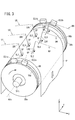
- FIG. 3 is a detailed view showing a state in which a sheet substrate is wound around the rotating drum shown in FIG. 2.
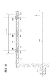
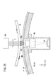
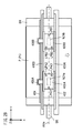
- FIG. 7 It is a figure which shows the state of the rotating drum shown in FIG. 7 before a cylindrical body and a side wall part are joined by welding. It is a figure for demonstrating the installation method to the rotating drum of the sensor circuit board shown in FIG. It is sectional drawing which shows the modification of the internal structure of the rotating drum shown in FIG. It is a figure which shows the structure of the sensor part installed in the opening part of the rotating drum shown in FIG. It is a figure for demonstrating the attachment method to the opening part of the sensor part shown in FIG. It is a figure which shows an example of the positional relationship of the mark formation area
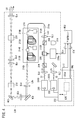
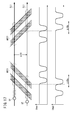
- FIG. 12 is a circuit block diagram showing the overall circuit configuration of the sensor circuit board shown in FIG. 9 and the circuit configurations of the three sensor units shown in FIG. It is a time chart figure explaining typically the mode of sampling which considered the signal delay at the time of wireless communication. It is a figure which shows the relationship between the feed amount of the subscanning direction measured by scanning the reference
- FIG. It is a figure showing thin film glass in modification 2.
- FIG. 1 is a diagram showing an overall configuration of a roll-to-roll type substrate processing apparatus (pattern exposure apparatus).
- the pattern of the electronic device is formed on the sheet substrate P (hereinafter also simply referred to as the substrate P) in the exposure unit main body (exposure apparatus, drawing apparatus) EX surrounded by the chamber CB.
- the exposure is performed on a photosensitive layer (photosensitive functional layer) such as a resist layer on the surface, a photosensitive silane coupling layer, or a film of an ultraviolet curable resin.
- a photosensitive layer photosensitive functional layer
- a plane parallel to the floor of a factory where the entire substrate processing apparatus is installed is defined as an XY plane of the orthogonal coordinate system XYZ, and a Z direction perpendicular to the XY plane is defined as a gravity direction.
- the long flexible sheet substrate P coated with the photosensitive layer and pre-baked is mounted on a rotating shaft protruding in the ⁇ Y direction from the supply roll mounting portion EPC1 while being wound around the supply roll FR.
- the supply roll mounting portion EPC1 is provided on the side surface on the ⁇ X side of the unwinding / winding portion 10, and is configured to be finely movable in the ⁇ Y directions as a whole.
- the sheet substrate P drawn from the supply roll FR includes an edge sensor Eps1 attached to a side surface parallel to the XZ plane of the unwinding / winding unit 10, a plurality of rollers having a rotation axis parallel to the Y axis, and a tension. It is sent to a cleaning roller CUR1 attached to the cleaner unit 11 adjacent in the + X direction via a tension roller RT1 that performs application and tension measurement.
- the cleaning roller CUR1 is processed so that the outer peripheral surface has adhesiveness, and rotates in contact with each of the front and back surfaces of the sheet substrate P, thereby removing particles and foreign matters attached to the front and back surfaces of the sheet substrate P. It consists of two rollers to be removed.
- the sheet substrate P that has passed through the cleaning roller CUR1 of the cleaner unit 11 passes through the nip roller NR1 provided to protrude in the ⁇ Y direction from the XZ surface of the tension adjusting unit 12, and the chamber CB of the exposure unit main body EX via the tension roller RT2. Is carried into the exposure unit main body EX through an opening CP1 formed to extend in the Y direction in a slot shape on the side wall of the exposure unit.
- the surface of the sheet substrate P on which the photosensitive layer is formed is upward (+ Z direction) when passing through the opening CP1.
- the sheet substrate P subjected to the exposure processing in the exposure unit main body EX is carried out through the opening CP2 formed in the slot direction in the Y direction on the ⁇ Z side of the opening CP1 and on the side wall of the chamber CB.
- the sheet substrate P carried out through the opening CP2 is disposed adjacent to the ⁇ X direction via a tension roller RT3 and a nip roller NR2 provided to protrude in the ⁇ Y direction from the XZ surface of the tension adjusting unit 12.
- the cleaning roller CUR2 is configured similarly to the cleaning roller CUR1.
- the sheet substrate P that has passed through the cleaning roller CUR2 of the cleaner unit 11 is parallel to the tension roller RT4, the edge sensor Eps2, and the Y axis that are attached to the lower step of the side surface parallel to the XZ plane of the unwinding / winding unit 10. It is wound up by the collection roll RR through a plurality of rollers having a rotating shaft.
- the collection roll RR is provided at the lower part of the side surface on the ⁇ X side of the unwinding / winding unit 10 and is mounted on the rotation shaft of the collection roll mounting unit EPC2 configured to be finely movable in the ⁇ Y direction as a whole.
- the collection roll RR winds up the sheet substrate P so that the photosensitive layer of the sheet substrate P faces the outer peripheral surface.
- the width direction (the short direction perpendicular to the long direction) of the surface (surface to be processed) of the sheet substrate P until it is pulled out from the supply roll FR and wound up by the collection roll RR. ) Is always conveyed in the longitudinal direction with the Y direction being in the Y direction.
- the supply roll FR and the recovery roll RR are arranged side by side in the Z direction in the unwinding / winding unit 10, the work of exchanging rolls is simplified.
- a single substrate processing apparatus is configured to perform an exposure process on the sheet substrate P by a roll-to-roll method, but an application unit and a drying unit that apply a photosensitive layer to the surface of the sheet substrate P are provided.
- the wet processing unit and the drying unit that are provided between the supply roll FR and the exposure unit main body EX or perform wet processing such as development processing and plating processing on the sheet substrate P after the exposure processing are collected with the exposure unit main body EX. It may be provided between the rolls RR.
- Each of the supply roll mounting part EPC1 and the recovery roll mounting part EPC2 has a rotation shaft for mounting a roll on which a protective sheet for protecting the surface to be processed of the sheet substrate P is wound. It is installed in parallel with the rotation axis of the collection roll RR.
- the supply roll mounting unit EPC1 includes a servo motor and a gear box (decelerator) that applies a predetermined rotational torque to the supply roll FR, and the servo motor is based on a tension amount measured by the tension roller RT1. Servo controlled by the control unit.
- the collection roll mounting unit EPC2 includes a servo motor and a gear box (decelerator) that applies a predetermined rotational torque to the collection roll RR, and the servo motor is transported based on the tension amount measured by the tension roller RT4. Servo controlled by the control unit of the mechanism.
- the measurement information from the edge sensor Eps1 that measures the displacement in the Y direction of one end portion (edge portion) of the sheet substrate P is the servo that moves the supply roll mounting portion EPC1 (and supply roll FR) in the ⁇ Y direction.
- the positional deviation in the Y direction of the sheet substrate P that is sent to the motor drive control unit and passes through the edge sensor Eps1 toward the exposure unit main body EX is always kept within a predetermined allowable range.
- the measurement information from the edge sensor Eps2 that measures the displacement in the Y direction of one end portion (edge portion) of the sheet substrate P moves the recovery roll mounting portion EPC2 (and the recovery roll RR) in the ⁇ Y direction. Uneven winding of the sheet substrate P is suppressed by moving the collection roll RR in the Y direction according to the positional deviation in the Y direction of the sheet substrate P passing through the edge sensor Eps2 and sent to the drive control unit of the servo motor.
- a step unit that extends in the X direction and is installed on the factory floor. 13 is provided.
- the step portion 13 has a width of several tens of centimeters in the Y direction so that the operator can go up and perform adjustment work and maintenance work. Further, in the step portion 13, incidental facilities such as various electric wirings, piping for air-conditioning gas, piping for cooling liquid, and the like are accommodated.
- a power supply unit 14 On the ⁇ Y direction side of the step portion 13, a power supply unit 14, a laser control unit 15 that controls a laser light source LSA (LSB) that generates an exposure beam, a laser light source LSA (LSB), and a deflector (see FIG. 5).
- Polygon mirror PM) and a chiller unit 16 that circulates a cooling liquid (coolant) for cooling a heat generating unit such as an optical modulator, and a temperature-controlled gas are supplied into the chamber CB of the exposure unit main body EX.
- An air conditioning unit 17 and the like are arranged.
- the nip roller NR1 and the tension roller RT2 attached to the tension adjusting unit 12 apply a substantially constant tension in the longitudinal direction (conveying direction) to the sheet substrate P on the upstream side of the exposure unit main body EX.
- the tension roller RT2 includes a tension measuring unit (sensor), and can be moved in the ⁇ Z direction in FIG. 1 by a servo motor so that the measured tension amount becomes a commanded value.
- the nip roller NR1 opposes two parallel rollers with a constant pressing force, and sandwiches the sheet substrate P between them while rotating one of the rollers with a servo motor so that the upstream side and the downstream side of the nip roller NR1.
- the tension applied to the sheet substrate P can be divided.
- the conveyance speed of the sheet substrate P can be actively controlled by rotationally driving one of the nip rollers NR1 by a servo motor. For example, if the servo motor of the nip roller NR1 is servo-locked to a stopped state (zero speed), The sheet substrate P can be locked (moored) at the position of the nip roller NR1.
- a substantially constant tension is applied to the sheet substrate P on the downstream side of the exposure unit main body EX in the longitudinal direction (conveyance direction) by the nip roller NR2 and the tension roller RT3 attached to the tension adjusting unit 12.
- the tension roller RT3 includes a tension measuring unit (sensor), and can be moved in the ⁇ Z direction in FIG. 1 by a servo motor so that the measured tension amount becomes a commanded value. Since the nip roller NR2 is actively controlled by a servo motor in the same manner as the nip roller NR1, the tension applied to the sheet substrate P can be divided between the upstream side and the downstream side of the nip roller NR2. By servo-locking the servo motor of the nip roller NR2 to a stopped state (zero speed), the sheet substrate P is locked (moored) at the position of the nip roller NR2.
- the supply roll FR is controlled by synchronously controlling the servo motor that rotationally drives the supply roll FR and the servo motor that rotationally drives the nip roller NR1 according to the amount of tension measured by the tension roller RT1.
- a predetermined tension is applied to the sheet substrate P in the conveyance path from the nip roller NR1 to the nip roller NR1.
- the nip roller NR2 and the collection roll RR A predetermined tension is applied to the sheet substrate P in the transport path up to.
- FIG. 2 is a view showing a detailed configuration of the exposure unit main body EX shown in FIG.
- the exposure unit main body EX has six drawing functions as a direct drawing type drawing head (exposure head, pattern forming head) for one-dimensionally scanning the spot light of the beam LB on the sheet substrate P by the polygon mirror PM and the f ⁇ lens FT.
- the beam for exposure (pulse beam in the ultraviolet wavelength region) LB from the unit Un (U1 to U6) and each of the two laser light sources LSA and LSB is distributed to the six beams LBn (LB1 to LB6) in a time-sharing manner.
- AM14 A beam distribution unit BDU supplied to each of the six drawing units Un (U1 to U6), and a plurality of alignment microscopes AM1m (AM11) for detecting an alignment mark MKm (see FIG. 6) formed on the sheet substrate P.
- AM14 AM2m
- Such a pattern drawing apparatus is disclosed in, for example, the pamphlet of International Publication No. WO2015 / 166910, and detailed description of the configuration from the laser light sources LSA and LSB to the respective drawing units U1 to U6 is omitted.
- the beam distribution unit BDU switches the drawing unit Un on which the beam LBn from the laser light source LSA is incident, for example, in the order of U1 ⁇ U3 ⁇ U5, so that the beam LBn from the laser light source LSA is drawn. Allocate to U1, U3, and U5 in a time-sharing manner.
- the beam distribution unit BDU switches the drawing unit Un on which the beam LB (LBn) from the laser light source LSB is incident in the order of U2 ⁇ U4 ⁇ U6, for example, so that the beam from the laser light source LSB.
- LBn is allocated to the drawing units U2, U4, and U6 in a time division manner.
- the sheet substrate P carried from the opening CP1 through the nip roller NR1 of the tension adjusting unit 12 is passed in the order of guide rollers R1, R2, rotating drum DR, guide rollers R3, R4, R5. Then, it exits from the opening CP2 of the exposure unit main body EX and moves toward the nip roller NR2.
- the rotary drum DR has a cylindrical outer peripheral surface having a constant radius from a rotation center axis (rotation center line) AXo parallel to the Y axis, and closely supports the sheet substrate P by about a half circumference in the + Z direction of the outer peripheral surface. .
- the rotary drum DR functions as a support member that supports the surface of the sheet substrate P so as to be a stable surface (cylindrical surface) when a pattern is exposed on the sheet substrate P, and includes a rotation drive mechanism DV1 including a motor and the like. It also functions as a movable stage member that feeds the surface of the sheet substrate P at a speed controlled in the longitudinal direction by the rotational drive.
- the rotation drive mechanism DV1 is controlled by a main control unit (control device) MCU.
- the amount of movement in the circumferential direction of the outer peripheral surface of the rotating drum DR is the scale portion of the outer peripheral surface of the scale disk SDa attached coaxially to the rotation center axis (center axis) AXo on the end side in the ⁇ Y direction of the rotating drum DR (
- the grid scale line SGp (see FIG. 3) is determined with submicron resolution by an encoder system that detects each of a plurality of encoder heads EC (EC0, EC1, EC2, EC3).
- the radius of the outer peripheral surface (scale surface) of the scale disk SDa and the radius of the outer peripheral surface of the rotary drum DR are substantially the same. Is acceptable.
- an origin mark Zpm that can be detected by each of the encoder heads EC0, EC1, EC2, and EC3 is formed at one place in the circumferential direction of the scale portion SGp of the scale disk SDa.
- the arrangement relationship of the encoder heads EC0 to EC3 is described in the aforementioned International Publication No. WO2015 / 166910 pamphlet, and further described in the International Publication No. WO2013 / 146184 pamphlet.
- the scanning locus of the spot light SP formed on the sheet substrate P by the beams LB1, LB3, and LB5 scanned by the odd-numbered drawing units U1, U3, and U5, respectively.
- the drawing lines (scanning lines) SL1, SL3, and SL5 are parallel to the rotation center axis AXo and arranged in a line at a certain interval in the Y direction.
- drawing lines which are scanning trajectories of the spot light SP formed on the sheet substrate P by the beams LB2, LB4, LB6 scanned by the even-numbered drawing units U2, U4, U6, respectively.
- SL4 and SL6 are also arranged in a row in parallel with the rotation center axis AXo and at a constant interval in the Y direction.
- a scale disk SDb having the same configuration as the scale disk SDa is coaxially attached to the shaft Sft on the + Y direction end side of the rotary drum DR.
- the installation direction is set so as to match as much as possible in order to reduce the Abbe error during measurement.
- the odd-numbered drawing lines SL1, SL3, and SL5 and the even-numbered drawing lines SL2, SL4, and SL6 are separated by a predetermined angle in the circumferential direction of the rotary drum DR, and each of the six drawing lines SL1 to SL6.
- the pattern to be drawn is spliced in the Y direction (width direction) on the sheet substrate P.
- a region surrounded by the six drawing lines SL1 to SL6 is a projected region of the beam LBn (LB1 to LB6).
- the encoder heads EC1a and EC2a are arranged to face the scale disk SDa, and the encoder heads EC1b and EC2b are arranged to face the scale disk SDb.
- the encoder head EC3a composed of the encoder head EC3a facing the scale disk SDa and the encoder head EC3b facing the scale disk SDb shown in FIG.
- Each mark detection area (observation field area) of the alignment microscope AM2m (four alignment microscopes AM21 to AM24 including four microscope objective lenses arranged in the Y direction) located downstream of the projection area (drawing lines SL1 to SL6) It is installed in the same direction as the circumferential direction of Vw2m (Vw21 to Vw24) (see FIG. 6).
- Measurement signals output from each of the encoder heads EC0a, EC0b, EC1a, EC1b, EC2a, EC2b, EC3a, and EC3b in accordance with a change in the circumferential direction of the scale portion SGp (scale line) of the scale disks SDa and SDb.
- a two-phase signal having a phase difference of 90 degrees or the like) and an origin signal (pulse) output at the moment when the origin mark Zpm is detected are sent to the counter unit ECNT.
- the counter unit ECNT is a plurality of digital counter circuits (not shown) for counting the circumferential position change of the scale unit SGp (scale line) with submicron resolution based on the measurement signals from the encoder heads EC0 to EC3.
- the count value of each digital counter circuit is reset to zero (or a default value) in response to the origin signal from the corresponding encoder head EC.
- the count value counted by each digital counter circuit corresponds to the circumferential distance or movement amount from the origin mark Zpm on the outer peripheral surface of the rotary drum DR, and these count values are the rotational drive of the rotary drum DR.
- Control of rotational speed by mechanism DV1 position monitoring of sheet substrate P in the sub-scanning direction (circumferential direction of outer peripheral surface of rotating drum DR) during pattern drawing, positioning control when rotating drum DR is stopped at a specific angular position Used for etc.
- the count value counted by each of the plurality of digital counter circuits of the counter unit ECNT is sent to the main control unit MCU.
- FIG. 4 is a diagram showing the configuration of the laser light sources LSA and LSB. Since the two laser light sources LSA and LSB have the same configuration, the configuration of the laser light source LSA will be described as a representative.
- a laser light source LSA as a fiber laser device includes light source units 200S and 202S, a polarizing beam splitter 204, an electro-optical element 206 as a drawing light modulator, a drive circuit 206a for the electro-optical element 206, a polarizing beam splitter 208, and an absorber.
- a fiber light amplification unit 216 a fiber light amplification unit 216, wavelength conversion optical elements 218 and 220, a control circuit 222 including a clock generator 222a, lenses GL1 to GL3, GLa to GLe, and reflection mirrors MC1 and MC2.
- the light source unit 200S includes a semiconductor laser element 200 that generates pulsed seed light (laser light) in an infrared wavelength region at a predetermined frequency (oscillation frequency, light emission frequency) Fs, and seed light (pulse light) from the semiconductor laser element 200.
- a semiconductor laser element 200 that generates pulsed seed light (laser light) in an infrared wavelength region at a predetermined frequency (oscillation frequency, light emission frequency) Fs, and seed light (pulse light) from the semiconductor laser element 200.
- Fs predetermined frequency
- seed light pulse light from the semiconductor laser element 200.
- Is shortened to a picosecond order and has an optical functional member (not shown, but a Q switch or the like) that has a high peak intensity and a sharp or sharp pulsed seed light S1.
- the optical functional member becomes unnecessary depending on the driving method of the semiconductor laser element 200.
- the light source unit 202S includes a semiconductor laser element 202 that generates a pulsed infrared wavelength range seed light (laser light) S2 having a low peak intensity at a predetermined frequency Fs and being slow (broadly broad).
- the seed light S1 emitted from the light source unit 200S and the seed light S2 emitted from the light source unit 202S have substantially the same energy per pulse, but the polarization states are different from each other, and the peak intensity is higher in the seed light S1. high.
- the seed lights S1 and S2 are both linearly polarized light, the polarization direction of the seed light S1 is S-polarized light, and the polarization direction of the seed light S2 is S-polarized light orthogonal to the P-polarized light.
- the semiconductor laser elements 200 and 202 are controlled to emit light in response to the clock signal LTC (predetermined frequency Fs) generated by the clock generator 222a by electrical control of the control circuit 222.
- the control circuit 222 is controlled by the main control unit MCU.
- the predetermined frequency Fs is determined according to the magnification correction information CMg sent from the main control unit MCU.
- the seed light S1 emitted while diverging from the light source unit 200S is converted into a parallel light flux by the lens GL1, and then enters the polarization beam splitter 204.
- the front focal point of the lens GL1 is set at the exit end of the light source unit 200S.
- the seed light S2 emitted while diverging from the light source unit 202S is collimated by the lens GL2, and then enters the polarization beam splitter 204.
- the front focal point of the lens GL2 is also set at the exit end of the light source unit 200S.
- the polarization beam splitter 204 transmits the S-polarized seed light S1 to the electro-optical element 206 and reflects the P-polarized seed light S2 to the electro-optical element 206.
- the electro-optic element 206 is transmissive to the seed lights S1 and S2, and for example, an electro-optic modulator (EOM: Electro-Optic Modulator) is used.
- EOM Electro-Optic Modulator
- the electro-optic element 206 responds to the on / off state (high / low) of the pattern data corresponding to the drawing unit Un on which the beam LB (LBn) is incident, and the seed lights S1 and S2 that have passed through the polarization beam splitter 204.
- the polarization state is switched by the drive circuit 206a.
- the seed light S1 and S2 from each of the DFB semiconductor laser element 200 and the DFB semiconductor laser element 202 has a long wavelength range of 800 nm or more, and therefore, the electro-optical element 206 having a polarization state switching response of about GHz is used. Can do.
- the seed lights S 1 and S 2 that have passed through the electro-optic element 206 are incident on the polarization beam splitter 208.
- Pattern data (drawing data) is provided for each drawing unit Un (U1 to U6) and is stored in the main control unit MCU.
- the pattern data corresponding to each drawing unit Un (U1 to U6) is the spot light SP of the beam LBn (LB1 to LB6) projected on the sheet substrate P from the pattern drawn by each drawing unit Un (U1 to U6).
- the plurality of pixels are each represented by logical information (pixel data) corresponding to the pattern. That is, in this pattern data, the direction along the main scanning direction (Y direction) of the spot light SP is the row direction, and the direction along the sub-scanning direction (conveying direction, X direction) of the sheet substrate P is the column direction.
- the bitmap data is composed of logical information of a plurality of pixels decomposed in two dimensions.
- the logical information of this pixel is 1-bit data of “0” or “1”.
- the logical information of “0” means that the intensity of the spot light SP projected on the sheet substrate P is set to a low level (non-drawing), and the logical information of “1” is the spot light SP projected on the sheet substrate P. This means that the strength of the image is set to a high level (drawing).
- the logical information of the pixels for one column of the pattern data corresponds to one drawing line SLn (SL1 to SL6). Therefore, the number of pixels for one column is determined according to the size of the pixels on the irradiated surface of the sheet substrate P and the length of the drawing lines SLn (SL1 to SL6).
- the intensity of the spot light SP of the beam LBn (LB1 to LB6) projected onto the sheet substrate P along one drawing line SLn (SL1 to SL6) is modulated according to the logical information of the pixels for one column.
- This logical information of the pixels for one column is called serial data DLn. That is, the pattern data is bitmap data in which serial data DLn are arranged in the column direction.
- the serial data DLn corresponding to the drawing unit U1 is DL1
- the serial data DLn corresponding to the drawing units U2 to U6 is DL2 to DL6.
- the drawing unit Un to which the beam LB (LBn) from the laser light source LSA is incident is switched in the order of U1 ⁇ U3 ⁇ U5, for example, the main control unit MCU is synchronized with the laser light source LSA.
- the serial data DLn to be output to the driving circuit 206a is output in the order of DL1-> DL3-> DL5.
- the drawing unit Un on which the beam LB (LBn) from the laser light source LSB is incident is switched in the order of U2 ⁇ U4 ⁇ U6, for example, the main control unit MCU
- the serial data DLn output to the drive circuit 206a of the laser light source LSB is output in the order of DL2-> DL4-> DL6.
- the electro-optical element 206 guides the incident seed light S1 and S2 to the polarization beam splitter 208 as they are without changing the polarization state.
- the electro-optical element 206 changes the polarization state of the incident seed light S1 and S2 (changes the deflection direction by 90 degrees) and performs polarization. Guide to beam splitter 208. Therefore, when the logical information of the pixel is “1”, the S-polarized seed light S1 is converted into P-polarized light, and the P-polarized seed light S2 is converted into S-polarized light.
- the polarization beam splitter 208 transmits the P-polarized light and guides it to the incident side end 216a of the fiber light amplifying unit 216 via the lens GL3, and reflects the S-polarized light to the absorber 210. Therefore, the polarization beam splitter 208 guides only one of the incident seed lights S1 and S2 to the incident side end 216a.
- the seed light transmitted through the polarization beam splitter 208 is referred to as Lse.
- the absorber 210 is an optical trap that absorbs the seed light S1 (S2) in order to suppress leakage of the seed light S1 (S2) to the outside.
- the seed light Lse converges at a predetermined NA (numerical aperture) and enters the incident side end 216a.
- the predetermined NA depends on the diameter of the spot light SP projected onto the sheet substrate P, but is set to about 0.04 to 0.08 in the present embodiment.
- the fiber optical amplifier 216 has a two-stage configuration in which fiber optical amplifiers 213A and 213B are connected in series. Therefore, pump light sources (excitation light sources) 212A and 212B and combiners 214A and 214B are provided corresponding to the fiber optical amplifiers 213A and 213B, respectively.
- the seed light Lse incident on the incident side end 216a of the fiber light amplifier 216 is first guided to the combiner 214A.
- the combiner 214A combines the seed light Lse incident on the incident side end 216a and the excitation light generated by the pump light source 212A and outputs the combined light to the first-stage fiber optical amplifier (preamplifier unit) 213A.
- the fiber optical amplifier 213A is doped with a laser medium that is excited by excitation light. Therefore, in the fiber optical amplifier 213A that transmits the synthesized seed light Lse and pump light, the seed light Lse is amplified by exciting the laser medium with the pump light.
- a laser medium doped in the fiber optical amplifier 213A a rare earth element such as erbium (Er), ytterbium (Yb), thulium (Tm), or the like is used.
- the seed light Lse amplified by the first-stage fiber optical amplifier 213A is guided to the combiner 214B.
- the combiner 214B combines the seed light Lse amplified by the fiber optical amplifier 213A and the pumping light generated by the pump light source 212B, and outputs the combined light to the second-stage fiber optical amplifier (main amplifier unit) 213B.
- the fiber optical amplifier 213B is doped with a laser medium that is excited by excitation light. Therefore, in the fiber optical amplifier 213B in which the synthesized seed light Lse and excitation light are transmitted, the seed light Lse is further amplified by exciting the laser medium with the excitation light.
- the seed light Lse amplified by the fiber optical amplifier 213B is emitted from the emission side end portion 216b of the fiber light amplification unit 216, and its optical path is turned back by the reflection mirrors MC1 and MC2 to the first-stage wavelength conversion optical element 218.
- the seed light Lse emitted from the emission side end portion 216b is referred to as a beam LBs.
- a lens GLa is provided between the exit-side end 216b and the mirror MC1, and the lens GLa converts the emitted beam LBs from the exit-side end 216b with a predetermined numerical aperture (NA) into a parallel light beam.
- the lens GLb provided between the mirror MC1 and the mirror MC2 converges the parallel beam LBs at the center of the first-stage wavelength conversion optical element 218.
- the wavelength conversion optical element 218 converts the wavelength of the incident beam LBs, and converts it into a harmonic beam LBs having a wave number three times that of the incident beam LBs.
- the beam LBs wavelength-converted by the wavelength conversion optical element 218 enters the second-stage wavelength conversion optical element 220 through the lenses GLc and GLd.
- the lens GLc collimates the incident beam LBs while diverging, and the lens GLd converges the collimated beam LBs at the center of the second-stage wavelength conversion optical element 220.
- the wavelength conversion optical element 220 converts the wavelength of the incident beam LBs, and converts it into a harmonic beam LBs having a wave number twice that of the incident beam LBs.
- the beam LBs wavelength-converted by the wavelength conversion optical element 220 is incident on the lens GLe while diverging, and is converted into a parallel light beam by the lens GLe.
- the beam LBs converted into the parallel light flux is emitted from the laser light source LSA as an ultraviolet wavelength beam (for example, a beam having a wavelength of 355 nm) LB.
- the emission side end portion 216b of the fiber light amplifying unit 216 and the center portion of the wavelength conversion optical element 218 are set in an optically conjugate relationship by the lenses GLa and GLb, and the center of the wavelength conversion optical element 218 is set.
- the central portion of the wavelength conversion optical element 220 are set in an optically conjugate relationship by the lenses GLc and GLd.
- the incident beam LBs is condensed as a beam waist, and the positions of the beam waists are beams LB1 to LB6 projected from the respective drawing units U1 to U6.
- the rear focal position of the lens GLe is set to the position of the exit window of the beam LB of the laser light source LSA.
- the optical member in the beam distribution unit BDU so that the rear focal position of the lens GLe (the exit window of the laser light source LSA) is conjugate with the entrance pupil position of the f ⁇ lens FT on which the reflection surface RP of the polygon mirror PM is located. (Lenses, mirrors, etc.) and optical members (lenses, mirrors, etc.) in each of the drawing units U1-U6 are arranged.
- the seed light Lse output from the polarization beam splitter 208 becomes the seed light S2
- the seed light S2 Is incident on the fiber light amplifier 216.
- This seed light S2 has a low peak intensity of the pulse and has a broad and slow characteristic.
- the fiber light amplifying unit 216 has low amplification efficiency for the seed light S2 having such a low peak intensity. Therefore, the beam LB output from the laser light source LSA becomes light that is not amplified to the energy required for exposure. Therefore, in this case, from the viewpoint of exposure, the laser light source LSA has substantially the same result as not emitting the beam LB.
- the intensity of the spot light SP projected on the sheet substrate P is extremely low.
- the ultraviolet beam LB derived from the seed light S2 has a slight intensity.
- the seed light Lse output from the polarization beam splitter 208 becomes the seed light S1
- the seed light S1 is input to the fiber light amplifying unit 216.
- This seed light S1 is sharp or sharp pulse light and has a high peak intensity, so that it is efficiently amplified by the fiber light amplifier 216.
- a beam LB having energy necessary for exposure of the sheet substrate P is output from the laser light source LSA. Thereby, the intensity of the spot projected on the sheet substrate P becomes a high level.
- the drawing line SLn of the drawing unit Un is set within the range of the maximum drawing length in which the drawing unit Un can scan the spot light SP of the beam LBn.
- the beam LBn is applied over the entire range of the maximum drawing length longer than the drawing line SLn. Spot light SP is projected. Note that the intensity of the beam LB1 projected to a position other than the drawing line SLn is at a low level.
- the drawing lines SLn (SL1 to SL6) referred to in the present embodiment refer to scanning lines in which the spot intensity is modulated by the serial data DLn (DL1 to DL6), that is, drawn. Therefore, the scanning period of the spot light SP along the drawing line SLn is substantially the same as the period in which the logic information of each pixel of the serial data DLn is output to the drive circuit 206a.
- each drawing unit Un (scanning unit, beam scanning device) Un will be described with reference to FIG. Since each drawing unit Un (U1 to U6) has the same configuration, only the drawing unit U1 will be described, and the description of the other drawing units Un will be omitted.
- the drawing unit Un irradiates the sheet substrate P with the beam LBn so that the beam LBn travels toward the rotation center axis AXo of the rotary drum DR. That is, the beam LBn traveling from the drawing unit Un toward the sheet substrate P is parallel to the normal line of the sheet substrate P with respect to the XZ plane. Further, each of the drawing units Un (U1 to U6) causes the beam LBn irradiated to the drawing lines SLn (SL1 to SL6) to be perpendicular to the irradiated surface of the sheet substrate P in a plane parallel to the YZ plane. Then, the beam LBn is irradiated toward the sheet substrate P.
- the beam LBn (LB1 to LB6) projected onto the sheet substrate P is scanned in a telecentric state with respect to the main scanning direction of the spot light SP on the irradiated surface.
- a line also referred to as an optical axis perpendicular to the irradiated surface of the sheet substrate P through each midpoint of a predetermined drawing line SLn (SL1 to SL6) defined by each drawing unit Un (U1 to U6), This is called the irradiation center axis Len (Le1 to Le6).
- the irradiation center axes Le1, Le3, Le5 of the odd-numbered drawing units U1, U3, U5 are in the same direction on the XZ plane, and the irradiation center axes Le2 of the even-numbered drawing units U2, U4, U6. , Le4, Le6 are in the same direction in the XZ plane (see FIG. 2).
- the direction parallel to the irradiation center axis Len (Le1) is defined as the Zt direction
- the direction in which the sheet substrate P is conveyed by the rotating drum DR on the plane orthogonal to the Zt direction is defined as the Xt direction
- the direction perpendicular to the Zt direction and perpendicular to the Xt direction is defined as the Yt direction. That is, the three-dimensional coordinates of Xt, Yt, and Zt in FIG. 5 are the same as the three-dimensional coordinates of X, Y, and Z in FIG. 2, and the Z-axis direction is parallel to the irradiation center axis Len (Le1).
- the reflection mirror M10 As shown in FIG. 5, in the drawing unit U1, along the traveling direction of the beam LB1 from the incident position of the beam LB1 to the irradiated surface of the sheet substrate P, the reflection mirror M10, the beam expander BE, the reflection mirror M11, Polarization beam splitter PBS1, reflection mirror M12, shift optical member (parallel plate) SR, deflection adjustment optical member (prism) DP, field aperture FA, reflection mirror M13, ⁇ / 4 wavelength plate QW, cylindrical lens CYA, reflection mirror M14, A polygon mirror PM, an f ⁇ lens FT, a reflection mirror M15, and a cylindrical lens CYb are provided.
- an origin sensor (origin detector) OP1 for detecting the drawing start possible timing of the drawing unit U1 and reflected light from the irradiated surface (sheet substrate P) are passed through the polarization beam splitter PBS1.
- an optical lens system G10 and a photodetector DT for detection are passed through the drawing unit U1 and reflected light from the irradiated surface (sheet substrate P).
- the beam LB1 incident on the drawing unit U1 travels in the ⁇ Zt direction and enters the reflection mirror M10 inclined by 45 ° with respect to the XtYt plane.
- the axis of the beam LB1 incident on the drawing unit U1 is incident on the reflection mirror M10 so as to be coaxial with the irradiation center axis Le1.
- the reflection mirror M10 functions as an incident optical member that causes the beam LB1 to enter the drawing unit U1, and the incident beam LB1 is moved from the reflection mirror M10 to the ⁇ Xt direction along the optical axis AXa set parallel to the Xt axis. Reflected in the -Xt direction toward the distant reflecting mirror M11.
- the optical axis AXa is orthogonal to the irradiation center axis Le1 in a plane parallel to the XtZt plane.
- the beam LB1 reflected by the reflection mirror M10 passes through the beam expander BE arranged along the optical axis AXa and enters the reflection mirror M11.
- the beam expander BE expands the diameter of the transmitted beam LB1.
- the beam expander BE includes a condensing lens Be1 and a collimating lens Be2 that collimates the beam LB1 that diverges after being converged by the condensing lens Be1.
- the reflection mirror M11 is disposed with an inclination of 45 ° with respect to the YtZt plane, and reflects the incident beam LB1 (optical axis AXa) toward the polarization beam splitter PBS1 in the ⁇ Yt direction.
- the polarization separation surface of the polarization beam splitter PBS1 disposed away from the reflection mirror M11 in the ⁇ Yt direction is disposed at an angle of 45 ° with respect to the YtZt plane, reflects the P-polarized beam, and is orthogonal to the P-polarized light. It transmits a linearly polarized (S-polarized) beam polarized in the direction. Since the beam LB1 incident on the drawing unit U1 is a P-polarized beam, the polarization beam splitter PBS1 reflects the beam LB1 from the reflection mirror M11 in the -Xt direction and guides it to the reflection mirror M12 side.
- the reflection mirror M12 is disposed with an inclination of 45 ° with respect to the XtYt plane, and reflects the incident beam LB1 in the ⁇ Zt direction toward the reflection mirror M13 that is separated from the reflection mirror M12 in the ⁇ Zt direction.
- the beam LB1 reflected by the reflection mirror M12 passes through the shift optical member SR, the deflection adjustment optical member DP, and the field aperture (field stop) FA along the optical axis AXc parallel to the Zt axis, and reaches the reflection mirror M13. Incident.
- the shift optical member SR two-dimensionally adjusts the center position in the cross section of the beam LB1 in a plane (XtYt plane) orthogonal to the traveling direction (optical axis AXc) of the beam LB1.
- the shift optical member SR is composed of two quartz parallel plates Sr1 and Sr2 arranged along the optical axis AXc.
- the parallel plate Sr1 can be tilted about the Xt axis, and the parallel plate Sr2 is Yt axis. Can be tilted around.
- the parallel plates Sr1 and Sr2 are inclined about the Xt axis and the Yt axis, respectively, so that the position of the center of the beam LB1 is shifted two-dimensionally by a minute amount on the XtYt plane orthogonal to the traveling direction of the beam LB1.
- the parallel plates Sr1 and Sr2 are driven by an actuator (drive unit) (not shown) under the control of the main control unit MCU.
- the deflection adjusting optical member DP finely adjusts the inclination of the beam LB1 reflected by the reflecting mirror M12 and passing through the shift optical member SR with respect to the optical axis AXc.
- the deflection adjusting optical member DP is composed of two wedge-shaped prisms Dp1 and Dp2 arranged along the optical axis AXc, and each of the prisms Dp1 and Dp2 is provided so as to be able to rotate 360 ° about the optical axis AXc. It has been.
- the axis of the beam LB1 reaching the reflecting mirror M13 and the optical axis AXc are made parallel, or the axis of the beam LB1 reaching the irradiated surface of the sheet substrate P and Parallel to the irradiation center axis Le1 is performed.
- the beam LB1 after the deflection adjustment by the two prisms Dp1 and Dp2 may be laterally shifted in a plane parallel to the cross section of the beam LB1, and the lateral shift is caused by the previous shift optical member SR. Can be returned to.
- the prisms Dp1 and Dp2 are driven by an actuator (drive unit) (not shown) under the control of the main control unit MCU.
- the beam LB1 that has passed through the shift optical member SR and the deflection adjustment optical member DP passes through the circular aperture of the field aperture FA and reaches the reflection mirror M13.
- the circular aperture of the field aperture FA is a stop that cuts a portion below the intensity of 1 / e 2 of the peak intensity at the base of the intensity distribution in the cross section of the beam LB1 expanded by the beam expander BE. If the circular aperture of the field aperture FA is a variable iris diaphragm whose diameter can be adjusted, the intensity (luminance) of the spot light SP can be adjusted.
- the reflection mirror M13 is disposed with an inclination of 45 ° with respect to the XtYt plane, and reflects the incident beam LB1 toward the reflection mirror M14 in the + Xt direction.
- the beam LB1 reflected by the reflection mirror M13 enters the reflection mirror M14 via the ⁇ / 4 wavelength plate QW and the cylindrical lens CYa.
- the reflection mirror M14 reflects the incident beam LB1 toward the polygon mirror (rotating polygonal mirror, scanning deflection member) PM.
- the polygon mirror PM reflects the incident beam LB1 toward the + Xt direction toward the f ⁇ lens FT having the optical axis AXf parallel to the Xt axis.
- the polygon mirror PM deflects (reflects) the incident beam LB1 in a one-dimensional manner in a plane parallel to the XtYt plane in order to scan the spot light SP of the beam LB1 on the irradiated surface of the sheet substrate P.
- the polygon mirror PM has a rotation axis AXp extending in the Zt-axis direction and a plurality of reflection surfaces RP formed around the rotation axis AXp (in this embodiment, the number Np of reflection surfaces RP is eight). ).
- the reflection direction of the beam LB1 is deflected by the single reflection surface RP, and the spot light SP of the beam LB1 irradiated on the irradiated surface of the sheet substrate P is converted into the main scanning direction (the width direction of the sheet substrate P, the Yt direction ) Can be scanned.
- the spot light SP of the beam LB1 can be scanned along the main scanning direction by one reflecting surface RP.
- the number of times the spot light SP is scanned along the drawing line SL1 on the irradiated surface of the sheet substrate P by one rotation of the polygon mirror PM is eight times the same as the number of the reflecting surfaces RP.
- the polygon mirror PM is rotated at a constant speed by a rotation drive source (for example, a digital motor capable of finely adjusting the rotation speed) RM under the control of the main control unit MCU.
- a rotation drive source for example, a digital motor capable of finely adjusting the rotation speed
- the effective drawing length (for example, 30 to 50 mm) of the drawing line SL1 is longer than the maximum scanning length (for example, about 1 mm longer than the effective drawing length by which the spot light SP can be scanned by the polygon mirror PM 31.
- the center point of the drawing line SL1 (the point through which the irradiation center axis Le1 passes) is set at the center of the maximum scanning length. Note that normal drawing is performed within the range of the effective drawing length, but if it is within the range of the maximum scanning length, drawing with the spot light SP is possible as necessary.
- the cylindrical lens CYa converges the incident beam LB1 on the reflection surface RP of the polygon mirror PM in the non-scanning direction (Zt direction) orthogonal to the main scanning direction (rotation direction) of the polygon mirror PM. That is, the cylindrical lens CYa converges the beam LB1 in a slit shape (ellipse shape) extending in a direction parallel to the XtYt plane on the reflection surface RP.
- a slit shape ellipse shape
- the influence can be suppressed.
- the irradiation position of the beam LB1 (drawing line SL1) irradiated on the irradiated surface of the sheet substrate P is suppressed from being shifted in the Xt direction due to a slight tilt error for each reflecting surface RP of the polygon mirror PM. Can do.
- the f ⁇ lens FT having the optical axis AXf extending in the Xt-axis direction is a telecentric scan lens that projects the beam LB1 reflected by the polygon mirror PM onto the reflection mirror M15 so as to be parallel to the optical axis AXf on the XtYt plane. It is.
- the incident angle ⁇ of the beam LB1 to the f ⁇ lens FT changes according to the rotation angle ( ⁇ / 2) of the polygon mirror PM.
- the f ⁇ lens FT projects the beam LB1 to the image height position on the irradiated surface of the sheet substrate P in proportion to the incident angle ⁇ through the reflection mirror M15 and the cylindrical lens CYb.
- the reflection mirror M15 reflects the beam LB1 from the f ⁇ lens FT in the ⁇ Zt direction toward the sheet substrate P via the cylindrical lens CYb.
- the beam LB1 projected on the sheet substrate P is a minute diameter of about several ⁇ m (for example, 3 ⁇ m) on the irradiated surface of the sheet substrate P. Focused on the spot light SP. Further, the spot light SP projected on the irradiated surface of the sheet substrate P is one-dimensionally scanned by the polygon mirror PM along the drawing line SL1 extending in the Yt direction.
- the optical axis AXf of the f ⁇ lens FT and the irradiation center axis Le1 are on the same plane, and the plane is parallel to the XtZt plane. Therefore, the beam LB1 traveling on the optical axis AXf is reflected in the ⁇ Zt direction by the reflecting mirror M15, and is projected on the sheet substrate P coaxially with the irradiation center axis Le1.
- at least the f ⁇ lens FT functions as a projection optical system that projects the beam LB1 deflected by the polygon mirror PM onto the irradiated surface of the sheet substrate P.
- At least the reflecting members (reflecting mirrors M11 to M15) and the polarizing beam splitter PBS1 function as an optical path deflecting member that bends the optical path of the beam LB1 from the reflecting mirror M10 to the sheet substrate P.
- the incident axis of the beam LB1 incident on the reflecting mirror M10 and the irradiation center axis Le1 can be made substantially coaxial.
- the beam LB1 passing through the drawing unit U1 passes through a substantially U-shaped or U-shaped optical path, and then travels in the ⁇ Zt direction and is projected onto the sheet substrate P.
- the spot light of the beam LBn (LB1 to LB6) is generated by each drawing unit Un (U1 to U6).
- the spot light SP can be relatively two-dimensionally scanned on the irradiated surface of the sheet substrate P by scanning the SP one-dimensionally in the main scanning direction (Y direction).
- the effective length of the drawing lines SLn (SL1 to SL6) is set to 30 mm, and the effective size ⁇ is overlapped by 1/2 of the spot light SP with 3 ⁇ m, that is, by 1.5 ⁇ m.
- the feeding speed (conveying speed) Vt of the sheet substrate P in the sub-scanning direction is 2.419 mm / sec and that the spot light SP is also scanned at intervals of 1.5 ⁇ m in the sub-scanning direction.
- the maximum incident angle (corresponding to the maximum drawing length of the spot light SP) at which the beam LB1 reflected by one reflecting surface RP of the polygon mirror PM effectively enters the f ⁇ lens FT is the focal length of the f ⁇ lens FT and the maximum drawing length It will be roughly decided by.
- the ratio (scanning efficiency) of the rotation angle ⁇ that contributes to actual scanning out of the rotation angle 45 degrees for one reflecting surface RP is ⁇ / 45 degrees.
- the rotation angle ⁇ that contributes to actual scanning is 15 degrees
- the origin sensor OP1 shown in FIG. 5 generates a pulsed origin signal SZ1 when the rotational position of the reflection surface RP of the polygon mirror PM reaches a predetermined position where the scanning of the spot light SP by the reflection surface RP can be started.
- the origin sensor OP1 generates the origin signal SZ1 when the angle of the reflection surface RP from which the spot light SP is scanned becomes a predetermined angular position. Since the polygon mirror PM has eight reflecting surfaces RP, the origin sensor OP1 outputs the origin signal SZ1 eight times during the period in which the polygon mirror PM rotates once.
- the origin signal SZ1 generated by the origin sensor OP1 is sent to the main control unit MCU.
- the origin signal SZ1 is information indicating the drawing start timing (scanning start timing) of the spot light SP by the drawing unit U1.
- the origin sensor OP1 includes a beam transmission system opa for emitting a laser beam Bga (continuous light emission) in a wavelength region that is non-photosensitive to the photosensitive functional layer of the sheet substrate P to the reflecting surface RP, and the reflecting surface RP.
- a beam receiving system opb that receives the reflected beam Bgb of the reflected laser beam Bga and generates an origin signal SZ1.
- the beam transmission system opa includes a light source that emits a laser beam Bga and an optical member (such as a reflection mirror or a lens) that projects the laser beam Bga emitted from the light source onto the reflection surface RP.
- the beam receiving system opb includes a light receiving unit including a photoelectric conversion element that receives the received reflected beam Bgb and converts it into an electrical signal, and an optical member that guides the reflected beam Bgb reflected by the reflecting surface RP to the light receiving unit. (Reflection mirror, lens, etc.).
- the beam transmission system opa and the beam reception system opb emit the beam transmission system opa when the rotation position of the polygon mirror PM comes to a predetermined position immediately before the scanning of the spot light SP by the reflection surface RP is started.
- the reflected beam Bgb of the laser beam Bga is provided at a position where the beam receiving system opb can receive it.
- the origin sensors OPn provided in the drawing units U2 to U6 are represented by OP2 to OP6, and the pulsed origin signals SZn generated by the origin sensors OP2 to OP6 are represented by SZ2 to SZ6.
- the main control unit MCU manages which drawing unit Un can scan the spot light SP from now on.
- the delay time Tdyn from when the origin signals SZ2 to SZ6 are generated until the spot light SP starts to be scanned along the drawing lines SL2 to SL6 by the drawing units U2 to U6 may be represented by Tdy2 to Tdy6.
- the photodetector DT shown in FIG. 5 has a photoelectric conversion element that photoelectrically converts incident light.
- a predetermined reference mark and reference pattern (see FIG. 13) are formed on the surface of the rotary drum DR.
- the region where the reference mark and the reference pattern are formed and the region where the reference mark and the reference pattern are not formed are set so that the reflectance with respect to the wavelength of the beam LB1 is different.
- the region where the reference mark and the reference pattern are formed is made of a material having a low reflectance (10 to 50%) with respect to the wavelength region of the beam LB1, and the region where the reference mark and the reference pattern are not formed.
- the spot light SP of the beam LB1 is irradiated from the drawing unit U1
- the reflected light is converted into a cylindrical lens CYb, a reflection mirror M15, an f ⁇ lens FT, a polygon mirror PM, a reflection mirror M14, a cylindrical lens CYa, and a ⁇ / 4 wavelength plate QW.
- the light passes through the reflection mirror M13, the field aperture FA, the deflection adjusting optical member DP, the shift optical member SR, and the reflection mirror M12 and enters the polarization beam splitter PBS1.
- a ⁇ / 4 wavelength plate QW is provided between the polarizing beam splitter PBS1 and the sheet substrate P, specifically, between the reflection mirror M13 and the cylindrical lens CYa.
- the beam LB1 irradiated to the sheet substrate P is converted from the P-polarized light to the circularly-polarized beam LB1 by the ⁇ / 4 wavelength plate QW, and from the reference mark and reference pattern (or the sheet substrate P) of the rotary drum DR.
- the reflected light (regular reflected light) returning to the polarization beam splitter PBS1 is converted from circularly polarized light to S-polarized light by the ⁇ / 4 wavelength plate QW. Therefore, the regular reflected light from the reference mark and reference pattern (or sheet substrate P) of the rotating drum DR passes through the polarization beam splitter PBS1 and enters the photodetector DT via the optical lens system G10.
- the outer peripheral surface of the rotating drum DR is irradiated with the spot light SP (its intensity is high level) two-dimensionally. . Therefore, by digitally sampling the change in the intensity of the photoelectric signal from the photodetector DT, the image information of the reference mark and the reference pattern formed on the rotary drum DR can be acquired.
- the change in the intensity of the photoelectric signal output from the photodetector DT is responsive to a clock signal LTC (produced by the laser light sources LSA and LSB) for pulse emission of the beam LB1 (spot light SP). Digital sampling is performed to obtain one-dimensional image data in the Yt direction.
- a certain distance in the sub-scanning direction (for example, 1/2 of the size ⁇ of the spot light SP)
- the main control unit MCU measures the inclination of the drawing line SL1 of the drawing unit U1 based on the acquired two-dimensional image information of the reference mark and reference pattern of the rotating drum DR.
- the inclination of the drawing line SL1 may be a relative inclination between the drawing units Un (U1 to U6), or may be an inclination (absolute inclination) with respect to the rotation center axis AXo of the rotary drum DR. Good. It goes without saying that the inclinations of the respective drawing lines SL2 to SL6 can be measured in the same manner.
- each drawing unit Un (U1 to U6) can be rotated (rotated) around the irradiation center axis Len (Le1 to Le6), each of the plurality of drawing units Un (U1 to U6). It is held by a body frame (not shown).
- each drawing line SLn (SL1 to SL6) also has an irradiation center axis on the irradiated surface of the sheet substrate P. It rotates around Len (Le1 to Le6). Accordingly, each drawing line SLn (SL1 to SL6) is inclined with respect to the Y direction.
- each drawing unit Un (U1 to U6) rotates around the irradiation center axis Len (Le1 to Le6), the beam LBn (LB1 to LB6) passing through each drawing unit Un (U1 to U6). And the relative positional relationship between the drawing units Un (U1 to U6) and the optical members in the drawing units Un (U1 to U6) do not change. Therefore, each drawing unit Un (U1 to U6) can scan the spot light SP along the drawing line SLn (SL1 to SL6) rotated on the irradiated surface of the sheet substrate P.
- the rotation of each drawing unit Un (U1 to U6) about the irradiation center axis Len (Le1 to Le6) is performed by an actuator (not shown) under the control of the main control unit MCU.
- the main control unit MCU rotates each of the drawing units Un (U1 to U6) around the irradiation center axis Len (Le1 to Le6) according to the measured inclination of each drawing line SLn, thereby The parallel state of the drawing lines SLn (SL1 to SL6) can be maintained. Further, when it is measured that the sheet substrate P or the exposure region W is distorted (deformed) based on the position of the mark MKm detected using the alignment microscopes AM1m and AM2m, a pattern to be drawn accordingly Need to be distorted.
- the main control unit MCU determines that the sheet substrate P and the exposure area W are distorted (deformed)
- the main control unit MCU moves the drawing unit Un (U1 to U6) around the irradiation center axis Len (Le1 to Le6).
- the respective drawing lines SLn are slightly inclined with respect to the Y direction according to the distortion (deformation) of the sheet substrate P and the exposure region W.
- the control is performed such that the pattern drawn along each drawing line SLn is expanded or contracted according to a specified magnification (for example, ppm order), or each drawing line SLn is individually set.
- a slight shift control in the main scanning direction Yt direction in FIG. 5). In this case, control is performed in consideration of the condition that patterns drawn on each of the drawing lines SLn (SL1 to SL6) adjacent to each other in the Y direction are joined together with good accuracy.
- the magnification of the drawing line SLn can be changed by shifting the oscillation frequency Fs from a reference frequency (for example, 100 MHz), that is, the drawing line SLn can be expanded or contracted.
- the drawing line SLn can be reduced by making the oscillation frequency Fs higher than the reference frequency, and the drawing line SLn can be extended by making the oscillation frequency Fs lower than the reference frequency. Since the oscillation frequency Fs is determined according to the magnification correction information CMg, the main control unit MCU outputs the magnification correction information CMg to the control circuit 222 of the laser light sources LSA and LSB, thereby changing the magnification of the drawing line SLn. be able to.
- the main control unit MCU can shift the drawing lines SLn (SL1 to SL6) along the main scanning direction by changing the delay time Tdyn (Tdy1 to Tdy6).
- the delay time Tdyn set so that the midpoint of the drawing line SLn becomes the midpoint of the maximum drawing length is set as a reference delay time, and the delay time Tdyn is made shorter than the reference delay time, so that the drawing line SLn is main-scanned. It can shift to the direction side opposite to the direction. Further, by making the delay time Tdyn longer than the reference delay time, the drawing line SLn can be shifted to the main scanning direction side.
- the main control unit MCU When the delay time Tdyn elapses after the origin sensor OPn generates the origin signal SZn, the main control unit MCU outputs the serial data DLn to the drive circuit 206a of the laser light source LSA (LSB). Thereby, the scanning of the spot light SP of the beam LBn is started.
- the irradiation center axis Len of the drawing unit Un and the axis (rotation center axis) on which the drawing unit Un actually rotates do not completely coincide with each other, they should be coaxial within a predetermined allowable range. That's fine.
- This predetermined allowable range is such that the drawing start point (or drawing end point) of the actual drawing line SLn when the drawing unit Un is rotated by the angle ⁇ sm, the irradiation center axis Len, and the rotation center axis are completely set.
- the drawing unit Un When the drawing unit Un is rotated by a predetermined angle ⁇ sm when it is assumed that they match, the amount of difference from the drawing start point (or drawing end point) of the designed drawing line SLn is the main scanning direction of the spot light SP Is set to be within a predetermined distance (for example, the size ⁇ of the spot light SP). Even if the optical axis of the beam LBn actually incident on the drawing unit Un does not completely coincide with the rotation center axis of the drawing unit Un, it is sufficient if it is coaxial within the above-described predetermined allowable range.
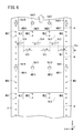
- FIG. 6 shows alignment marks MKm formed on the sheet substrate P, mark detection areas Vw1m and Vw2m of the alignment microscopes AM1m and AM2m on the sheet substrate P, and a drawing line SLn formed on the sheet substrate P.
- FIG. A plurality of marks MKm (MK1 to MK4) are reference marks for relatively aligning (aligning) a predetermined pattern drawn in the exposure area W on the irradiated surface of the sheet substrate P with the sheet substrate P. It is.
- the plurality of alignment microscopes AM1m (AM11 to AM14) and AM2m (AM21 to AM24) have a plurality of marks MKm (MK1 to MK4) on the sheet substrate P supported by the outer peripheral surface (circumferential surface) of the rotary drum DR. Is detected.
- the plurality of alignment microscopes AM1m (AM11 to AM14) are projected regions (drawing lines SL1) on the sheet substrate P of the spot light SP of the beams LBn (LB1 to LB6) irradiated from the plurality of drawing units Un (U1 to U6). To the upstream side (the ⁇ X direction side) of the sheet substrate P in the transport direction.
- the plurality of alignment microscopes AM2m are irradiated regions (drawings) on the sheet substrate P of the spot light SP of the beams LBn (LB1 to LB6) emitted from the plurality of drawing units Un (U1 to U6).
- the region surrounded by the lines SL1 to SL6) is provided on the downstream side (+ X direction side) in the conveyance direction of the sheet substrate P.
- the alignment microscopes AM1m (AM11 to AM14) and AM2m (AM21 to AM24) are a local region (observation field region) Vw1m including a light source that projects illumination light for alignment onto the sheet substrate P and a mark MKm on the surface of the sheet substrate P.
- Vw11 to Vw14 Vw2m (Vw21 to Vw24) an observation optical system (including an objective lens) for obtaining magnified images, and while the sheet substrate P is moving in the transport direction
- an image sensor such as a CCD or a CMOS that captures an image with a high-speed shutter according to the transport speed Vt.
- Imaging signals (image data) captured by each of the plurality of alignment microscopes AM1m (AM11 to AM14) and AM2m (AM21 to AM24) are sent to the main control unit MCU.
- the main control unit MCU detects the position (mark position information) of the mark MKm (MK1 to MK4) on the sheet substrate P by performing image analysis of the plurality of image pickup signals sent thereto.
- the illumination light for alignment is light in a wavelength region (non-photosensitive wavelength region) that has little sensitivity to the photosensitive functional layer on the sheet substrate P, for example, light having a wavelength of about 500 to 800 nm.
- the alignment illumination light can be monochromatic light having a peak at one wavelength in the non-photosensitive wavelength range, multicolor light having a peak in a plurality of wavelengths, or broadband light having a broad intensity distribution in the non-photosensitive wavelength range. Any of these may be used.
- a plurality of marks MK1 to MK4 are provided around each exposure area W.
- a plurality of marks MK1 and MK4 are formed on both sides of the exposure region W in the width direction of the sheet substrate P at a constant interval Dh along the longitudinal direction of the sheet substrate P.
- the mark MK1 is formed on the ⁇ Y direction side in the width direction of the sheet substrate P
- the mark MK4 is formed on the + Y direction side in the width direction of the sheet substrate P.
- Such marks MK1 and MK4 are located at the same position in the longitudinal direction (X direction) of the sheet substrate P when the sheet substrate P is not deformed due to a large tension or a thermal process. Arranged.
- the marks MK2 and MK3 are between the marks MK1 and MK4, and extend along the width direction (short direction) of the sheet substrate P in the margin part BLS between the + X direction side and the ⁇ X direction side of the exposure region W. Is formed.
- the mark MK2 is formed on the ⁇ Y direction side in the width direction of the sheet substrate P
- the mark MK3 is formed on the + Y direction side of the sheet substrate P.
- the distance in the Y direction between the mark MK1 and the mark MK2 in the margin part BLS arranged at the ⁇ Y direction side end of the sheet substrate P, the interval in the Y direction between the mark MK2 and the mark MK3 in the margin part BLS, and The interval in the Y direction between the mark MK4 arranged at the end on the + Y direction side of the sheet substrate P and the mark MK3 in the margin BLS is set to the same distance.
- These marks MKm (MK1 to MK4) may be formed together when the pattern layer of the first layer is formed. For example, when the pattern of the first layer is exposed, the mark pattern may be exposed around the exposure area W where the pattern is exposed.
- the mark MKm may be formed in the exposure area W. For example, it may be formed in the exposure area W along the outline of the exposure area W. Further, a pattern portion at a specific position or a specific shape portion in the pattern of the electronic device formed in the exposure region W may be used as the mark MKm.
- the alignment microscopes AM11 and AM21 are arranged so as to image the mark MK1 existing in the observation visual field regions (detection regions) Vw11 and Vw21 by the objective lens.
- the alignment microscopes AM12 to AM14 and AM22 to AM24 are arranged so as to image the marks MK2 to MK4 existing in the observation visual field regions Vw12 to Vw14 and Vw22 to Vw24 by the objective lens. Therefore, the plurality of alignment microscopes AM11 to AM14 and AM21 to AM24 correspond to the positions of the plurality of marks MK1 to MK4, and the sheet substrates in the order of AM11 to AM14 and AM21 to AM24 from the ⁇ Y direction side of the sheet substrate P. It is provided along the width direction of P.
- the distance between the exposure position (drawing lines SL1 to SL6) and the observation visual field region Vw1m (Vw11 to Vw14) with respect to the X direction is longer than the length of the exposure region W in the X direction. It is provided to be shorter.
- the distance between the exposure position (drawing lines SL1 to SL6) and the observation visual field region Vw2m (Vw21 to Vw24) in the X direction is the length of the exposure region W in the X direction. It is provided to be shorter.
- the number of alignment microscopes AM1m and AM2m provided in the Y direction can be changed according to the number of marks MKm formed in the width direction of the sheet substrate P. Further, the size of each observation visual field region Vw1m (Vw11 to Vw14) and Vw2m (Vw21 to Vw24) on the irradiated surface of the sheet substrate P depends on the size of the marks MK1 to MK4 and the alignment accuracy (position measurement accuracy). Although it is set, it is about 100 to 500 ⁇ m square.
- the sheet substrate P is conveyed.
- the state (whether or not it is distorted), the position of the exposure region W, the positions of the drawing lines SL1 to SL6 on the sheet substrate P, etc. can be grasped with high accuracy.
- sensor portions SEn (SE1 to SE6) as shown in FIG. 11 are provided corresponding to the positions of the plurality of drawing lines SLn (SL1 to SL6).
- the beam LBn transmitted through the margin part BLS is detected by the sensor.
- the photoelectric sensor PDi PD1 to PD3 of the part SEn.
- the blank portion BLS of the sheet substrate P is a transparent region. That is, the sheet substrate P is formed of a transparent material, and a pattern layer is formed in the circuit and wiring of the electronic device in the exposure region W of the sheet substrate P of the transparent material.
- FIG. 7 shows an external view of the rotary drum DR.
- the rotating drum DR has a cylindrical body (cylindrical tube) 50 having a certain radius from the rotation center axis AXo and a bendable thin plate having a thickness of 1 mm or less that is wound around and bonded to the entire outer peripheral surface of the cylindrical body 50. It has a sheet glass CG and a side wall 52 provided on the side surface of the cylindrical body 50 and having a shaft Sft. The cylindrical body 50 and the side wall 52 are joined by welding.
- the sheet glass (cover member, cover glass) CG can be bent to a diameter smaller than the diameter of the outer peripheral surface of the cylindrical body 50, and is, for example, glass having a thickness of 200 ⁇ m or less.
- the outer peripheral surface of the cylindrical body 50 is formed so that the sheet glass CG has a cylindrical surface shape having the same radius as that of the outer peripheral surface of the cylindrical body 50 or slightly larger than the radius of the outer peripheral surface of the cylindrical body 50. It is wrapped around Of the outer peripheral surface of the cylindrical body 50, a recess having a thickness of the sheet glass CG is formed in an area where the sheet glass CG is wound, so that the rotation from the rotation center axis AXo of the sheet glass CG wound around the cylindrical body 50 is achieved.
- the radius may coincide with the radius from the rotation center axis AXo of the outer peripheral surface of the cylindrical body 50 or may coincide with each other within a predetermined allowable range.
- the sheet glass CG is formed so that the length in the circumferential direction of the sheet glass CG wound around the cylindrical body 50 is slightly shorter than the length of the outer periphery of the cylindrical body 50. Therefore, when the sheet glass CG is wound around the cylindrical body 50, both end portions of the sheet glass CG are not adjacent to each other and a predetermined gap Gp is opened, but the gap Gp is filled with a resin, an adhesive, or the like. In addition, if the sheet glass CG is formed so that the circumferential length of the sheet glass CG wound around the cylindrical body 50 is the same as the outer peripheral length of the cylindrical body 50, the gap Gp does not occur. If the sheet glass CG is manufactured with high accuracy, the cost may increase.
- the cylindrical body 50 is provided with a plurality of openings 50 n (50 1 to 50 6 ) at positions in the Y direction corresponding to the plurality of drawing lines SLn. That is, the plurality of openings 50 n (50 1 to 50 6 ) are formed in a staggered arrangement in two rows along the circumferential direction of the rotary drum DR corresponding to the drawing lines SLn (SL1 to SL6).
- the dimension in the Y direction of the opening region of the opening 50 n is set so as to include the drawing line SLn, and the dimension in the X direction (circumferential direction) is set to a size that can accommodate the photoelectric sensors PDi (PD1 to PD3). Is done.
- Each of the plurality of openings 50 n (50 1 to 50 6 ) is formed at two locations that are 180 degrees apart in the circumferential direction of the cylindrical body 50.
- Each of the plurality of openings 50 n (50 1 to 50 6 ) is provided with a sensor unit SEn having the three photoelectric sensors PDi (PD1 to PD3) described above. That is, the sensor unit SE1 is provided in the opening 50 1 , and similarly, the sensor units SE2 to SE6 are provided in the openings 50 2 to 50 6 .
- the cylindrical body 50 has a plurality of openings 50 n (50 1 to 50 6 )
- the outer peripheral surface of the cylindrical body 50 is entirely covered with the sheet glass CG.
- the sheet substrate P is stably adhered and supported on the surface of the sheet glass CG curved in a cylindrical surface shape even on the plurality of openings 50 n (50 1 to 50 6 ). Significant deformation is prevented in the region corresponding to the portion 50 n (50 1 to 50 6 ).
- the blank portion BLS between the exposure area W and the exposure area W is formed. It is necessary to make the distance at least a half circumference of the rotating drum DR. Further, in the case where the plurality of openings 50 n (50 1 to 50 6 ) are provided at four positions that are 90 degrees apart in the circumferential direction of the cylindrical body 50, at least the margins BLS between the exposure area W and the exposure area W are provided. The distance needs to be at least 1/4 of the entire circumference of the rotating drum DR.
- the length in the circumferential direction is 1 ⁇ 2 or more of the total circumferential length of the outer peripheral surface of the rotary drum DR, or 1 / It is not necessary to set 4 or more.
- the margin part BLS set to a length of 1 ⁇ 2 or more of the entire circumference, or 1 ⁇ 4 or more of the entire circumference is, for example, every several to several tens of exposure areas W, and several to several tens of exposure areas W.
- the blank space BLS between them may be a quarter or less of the entire circumference.
- a light-shielding reference mark and a reference pattern made of chromium or the like are formed on the surface of the sheet glass CG.
- the photoelectric sensor (photoelectric detector) PDi is not interrupted by the light-shielding reference mark and reference pattern, and the sheet glass CG.
- the beam LBn that has passed through is received.
- the photoelectric sensor PD1 detects the beam LBn that has passed through the mark formation region RM1 on the sheet glass CG.
- the photoelectric sensors PD2 and PD3 detect the beam LBn transmitted through the mark formation regions RM2 and RM3 on the sheet glass CG.
- the reference mark and the reference pattern are etched by exposing a pattern with a photolithography exposure machine in a state where a light-shielding chromium layer is deposited on the surface of the sheet glass CG, and a resist is applied and the sheet glass CG is held flat. Is formed.
- the sheet glass CG on which the reference mark and the reference pattern are formed is wound around the surface of the cylindrical body 50, an alignment mark (not shown) previously engraved on the outer peripheral surface of the rotary drum DR, and the sheet glass CG Using alignment marks (not shown) formed on the periphery or the like, the sheet glass CG is wound around the surface of the cylindrical body 50 by aligning the position error and inclination error in the XY directions as small as possible. (to paste together).
- FIG. 8 is a view showing a state of the rotary drum DR shown in FIG. 7 before the cylindrical body 50 and the side wall 52 are joined by welding, and will be described in more detail with reference to FIG.
- the side wall 52 is provided with windows 52A and 52B for installing the sensor circuit board 60 (see FIGS. 7 and 9) and pedestals 54A and 54B.
- the inner wall surface of the window portion 52A on the rotation center axis AXo side and the installation surface of the sensor circuit board (electric circuit portion) 60 of the pedestal portion 54A are on the same plane, and the inner side of the window portion 52B on the rotation center axis AXo side.
- the wall surface and the installation surface of the sensor circuit board 60 of the pedestal 54B are flush with each other.
- the sensor unit SEn is connected to the sensor circuit board 60.
- the window portion 52A and the pedestal portion 54A, and the window portion 52B and the pedestal portion 54B are provided symmetrically about the rotation center axis AXo.
- the orientation of the center position in the circumferential direction of the window 52A and the pedestal 54A as viewed from the rotation center axis AXo and the odd-numbered openings 50 1 , 50 3 , 50 5 (or the drawing line SL1 as viewed from the rotation center axis AXo) , SL3, SL5) and the even-numbered openings 50 2 , 50 4 , 50 6 (or the drawing lines SL2, SL4, SL6) are cylindrical so that the azimuth of the center position in the circumferential direction is the same azimuth.
- the body 50 and the side wall 52 are welded.
- the radius from the rotation center axis AXo of the inner peripheral surface 50J of the cylindrical body 50 and the radius from the rotation center axis AXo of the outer peripheral surface 52C of the side wall portion 52 substantially coincide with each other.
- a side wall portion 52 having the same configuration as the side wall portion 52 provided on the side surface in the ⁇ Y direction is also provided on the side surface on the + Y direction side of the cylindrical body 50.
- On the pedestal portions 54A and 54B provided on the side wall portion 52 on the -Y direction side three sensor portions SE1 to SE3 provided in each of the three openings 50 1 to 50 3 corresponding to the drawing lines SL1 to SL3, A sensor circuit board 60 to be connected is installed.
- the pedestal portions 54A and 54B of the side wall portion 52 on the + Y direction side are connected to the sensor portions SE4 to SE6 provided in each of the three openings 50 4 to 50 6 corresponding to the drawing lines SL4 to SL6.
- a sensor circuit board 60 is installed.
- the shafts Sft protruding on both sides in the Y direction are aligned so as not to be eccentric with respect to the rotation center axis AXo.
- the welded cylindrical body 50 and the side wall 52 are in the state as shown in FIG. 9, but the eccentric error between the shaft Sft (rotation center axis AXo) and the outer peripheral surface of the cylindrical body 50, and the outer peripheral surface of the cylindrical body 50.
- the outer peripheral surface of the cylindrical body 50 is ground by a lathe and then the surface is polished to have a predetermined roughness (Ra value).
- An antireflection film having a predetermined reflectance (for example, 10% or less) in the wavelength region of the drawing beam LBn is deposited on the outer peripheral surface of the cylindrical body 50 after polishing (and the cross section of the opening 50 n ). Is done.
- FIG. 10 is a plane parallel to the YZ plane and including the rotation center axis AXo, showing a state in which the rotary drum DR is broken, and the shaft Sft has a length that protrudes by a predetermined length on both sides in the Y direction of the rotary drum DR. Consists of a single round bar.
- the shaft Sft is processed in advance by a precise lathe so that the shaft runout (linearity) error and the roundness error become several ⁇ m or less.
- a round hole that can penetrate the shaft Sft is formed at the center of the side wall portion 52 that is fitted to each of both sides in the Y direction of the cylindrical body 50, and the cylindrical body 50, the side wall portion 52, and the shaft Sft are combined as shown in FIG.
- FIG. 9 is a diagram for explaining a method of installing the sensor circuit board (electric circuit unit) 60 on the rotary drum DR.
- the cylindrical body 50 and the side wall 52 are joined together by welding, and the outer peripheral surface of the cylindrical body 50 is ground and polished to deposit an antireflection film (in a state where the sheet glass CG is not wound), and then the windows 52A and 52B.
- the sensor circuit board 60 is inserted from each of these, and the sensor circuit board 60 is installed on the pedestals 54A and 54B.
- the sensor circuit board 60 is fixed to the pedestals 54A and 54B with an adhesive or the like.
- the sensor circuit board 60 inserted from each of the windows 52A and 52B of the side wall 52 on the Y-direction side has three connectors for connecting to the sensors SE1 to SE3 provided in the openings 50 1 to 50 3 Portions CNT1 to CNT3 are provided. Similarly, the sensor circuit board 60 inserted from each of the windows 52A and 52B of the side wall 52 on the + Y direction side 3 is connected to the sensors SE4 to SE6 provided in the openings 50 4 to 50 6. Two connector portions CNT4 to CNT6 are provided (not shown). As will be described later with reference to FIG. 15, a wireless power supply unit 108, a secondary battery (chargeable battery) 110, a wireless communication unit 106, a microcomputer unit 104, and the like are mounted on the sensor circuit board 60. .
- the sensor unit SEn includes three sensor units SUi (SU1 to SU3), a planar board BDa parallel to the XY plane that supports the three sensor units SUi (SU1 to SU3), and a YZ plane connected to the board BDa. And a planar board (circuit board) BDb in parallel with each other. Since this sensor unit SEn is mounted in the rotating drum DR (cylindrical body 50) and rotates, the rotating drum DR is positioned in a state shown in FIG. 11 in the orthogonal coordinate system XYZ.
- the sensor unit SUi (SU1 to SU3) includes a photoelectric sensor PDi (PD1 to PD3) and a condenser lens LG.
- the photoelectric sensor PDi included in the sensor unit SU1 is referred to as PD1
- the photoelectric sensors PDi included in the sensor units SU2 and SU3 are referred to as PD2 and PD3.
- the condensing lens LG of the sensor unit SUi has an optical axis AXg parallel to the Z axis, and is composed of a convex lens that condenses the incident beam LBn on the light receiving surface of the photoelectric sensor PDi.
- the beam LBn can be guided to the photoelectric sensor PDi over a certain range (the aperture size of the condensing lens LG) in the drawing line SLn which is the scanning locus of the beam LBn.
- the three sensor units SUi (SU1 to SU3) are straight along the Y direction on the installation surface of the board BDa at equal intervals so that each optical axis AXg of the condenser lens LG is separated in the Y direction by a certain distance DHs. Is placed on top.
- the sensor unit SU2 is located between the sensor unit SU1 and the sensor unit SU3, the distance between the center position of the sensor unit SU1 and the center position of the sensor unit SU2, the center position of the sensor unit SU2, and the sensor The distance from the center position of the unit SU3 is the distance DHs.
- the photoelectric sensor PDi is provided in the sensor unit SUn so that the center position of the sensor unit SUn (the optical axis AXg of the condensing lens LG) matches the center position of the photoelectric sensor PDi.
- the planar board BDb is attached to the ⁇ Z direction side of the board BDa so as to be orthogonal to the installation surface of the board BDa.
- An amplifier Ampn (Amp1 to Amp3) that amplifies an analog electric signal detected by the photoelectric sensor PDi is attached to the surface on the + X direction side of the board BDb.
- the amplifier Amp1 amplifies the analog electric signal detected by the photoelectric sensor PD1.
- the amplifiers Amp2 and Amp3 amplify analog electric signals detected by the photoelectric sensors PD2 and PD3.
- a ribbon wire LW is connected to the surface on the + X direction side of the board BDb in order to output electric signals detected by the plurality of photoelectric sensors PDi (PD1 to PD3), and a sensor circuit board is connected to the tip of the ribbon wire LW.
- a socket PLGn is provided for connection to 60 connector parts CNTn (FIG. 9).
- the socket PLG1 of the sensor unit SE1 is connected to the connector unit CNT1.
- the sockets PLG2 to PLG6 of the sensor units SE2 to SE6 are connected to the connector units CNT2 to CNT6.
- the sensor circuit board 60 connected to the sensor parts SE1 to SE3 is attached to the base part 54A on the ⁇ Y direction side in the rotary drum DR (cylindrical body 50) and connected to the sensor parts SE4 to SE6.
- the sensor circuit board 60 is attached to the pedestal 54A on the + Y direction side in the rotary drum DR (cylindrical body 50).
- each of the six sensor portions SEn Two sensor circuit boards 60 to be connected are attached to the pedestal portions 54B on the + Y direction side and the ⁇ Y direction side in the rotary drum DR (cylindrical body 50).
- a supporting member 50M for supporting the board BDa of the sensor unit SE1 at a predetermined height position (a radial position) is provided in the vicinity of the opening 50 1 on the inner peripheral side of the cylindrical body 50.
- the support member 50M is attached to the inner peripheral surface 50J of the cylindrical body 50 before the side wall 52 is welded to the cylindrical body 50.
- the connector portion After the sensor circuit board 60 is fixed to the base portion 54A (54B), through a socket PLG1 and ribbon wire LW sensor unit SE1 in the opening 50 1, the connector portion while holding the socket PLG1 with a tool such as a dedicated pliers Connect to CNT1. Therefore, the length of the ribbon wire LW is set such that sufficient slack is generated. Thereafter, the board BDa of the sensor unit SE1 is fixed to the support member 50M. As a result, the sensor part SE1 is provided in the opening 50 1 . At this time, the extension line of the optical axis AXg of the condensing lens LG of each sensor unit SUi (SU1 to SU3) is set so as to pass through the rotation center axis AXo.
- each sensor unit SUi SE1 (SE1 to SE6) of each of the plurality of sensor portions SEn (SE1 to SE6).
- the sheet glass CG is a cylindrical body so that the mark formation regions RMi (RM1 to RM3) in which the reference marks and the reference patterns are formed are positioned at positions corresponding to the positions of the optical axes AXg of the condenser lenses LG of SU1 to SU3). Adhering to 50 outer peripheral surfaces.
- a multilayer film for adjusting the reflectance / transmittance may be deposited under the conditions disclosed in International Publication No. 2014/034161.
- the transmittance of the portion (mark formation region RMi) immediately above the condensing lens LG of the sheet glass CG may be set to be high in the wavelength region of the exposure beam LBn.
- FIG. 13 is a diagram illustrating an example of the positional relationship between the mark formation region RMi and the sensor unit SUi and the drawing line SLn.
- the mark formation region RM1 and the sensor unit SU1, and the mark formation region RM3 and the sensor unit SU3 are positioned on both ends of the drawing line SLn of the maximum drawing length (for example, 31 mm) of the spot light SP in the Y direction.
- the region RM2 and the sensor unit SU2 are located at the center of the drawing line SLn. With respect to the XY plane, the center position of the mark formation region RMi (RM1 to RM3) matches the center position of the sensor unit SUi (SU1 to SU3).
- the three mark formation regions RMi are arranged on a straight line along the Y direction at equal intervals with a constant distance DHs.
- Electrical signals output from each of the sensor units SUi (SU1 to SU3) when the spot light SP of the beam LBn scanned along the drawing line SLn scans the plurality of mark formation regions RMi (RM1 to RM3).
- the time interval of the (detection signal) and the shape of the signal waveform By comparing the time interval of the (detection signal) and the shape of the signal waveform, the isovelocity of the spot light SP along the drawing line SLn, the distortion of the drawing line SLn, the spots at both ends and the center of the drawing line SLn.
- Changes in the diameter of the light SP can be measured. These measurements are performed by the main control unit MCU. That is, the sensor circuit board 60 can communicate with the main control unit MCU, and the sensor circuit board 60 outputs signals output from the sensor units SUi (SU1 to SU6) to the main control unit MCU. Note that the sensor circuit board 60 may autonomously calculate signals output from the sensor units SUi (SU1 to SU6) to obtain measurement values.
- FIG. 14 is a diagram showing an example of the reference marks MPg1 to MPg3, MPx, MPy and the reference patterns MPC1, MPC2 formed in the mark formation region RMi.
- Each of the three reference marks MPg1 to MPg3 formed on the sheet glass CG discretely arranged in the Y direction has a line pattern (light shielding property) extending in the X direction (circumferential direction of the rotating drum DR) in the Y direction. It is a line and space pattern arranged at a constant pitch.
- Each of the plurality of reference marks MPg1 to MPg3 may be formed on the sheet glass CG so that the line width and the pitch of the line and space are different from each other.
- the reference mark MPx is a line pattern (light shielding property) extending in the Y direction
- the reference mark MPy is a line pattern (light shielding property) extending in the X direction.
- the two reference marks MPx and MPy cross in a cross shape.
- the reference marks MPx and MPy are formed on the sheet glass CG so that the center position of the reference mark MPx and the center position of the reference mark MPy cross each other.
- the reference patterns MPC1 and MPC2 are line and space in which line patterns (light shielding properties) extending in a direction inclined ⁇ 45 degrees with respect to the main scanning direction (Y direction) of the spot light SP are arranged at a constant pitch in the Y direction. is there.
- the center positions of the three reference marks MPg1 to MPg3 and the center positions of the two reference marks MPx and MPy are separated by a distance DXa in the X direction, and the center positions of the two reference marks MPx and MPy and the two reference patterns MPC1, Reference marks MPg1 to MPg3, MPx, MPy and reference patterns MCP1, MPC2 are formed on the sheet glass CG so that the center position of MPC2 is separated by a distance DXb with respect to the X direction.
- the three reference marks MPg1 to MPg3 are formed on the + X direction side of the mark formation region RMi (RM1 to RM3), and the two reference patterns MPC1 and MPC2 are on the ⁇ X direction side of the mark formation region RMi (RM1 to RM3). Is formed.
- the reference marks MPx and MPy are formed between the reference marks MPg1 to MPg3 and the two reference patterns MPC1 and MPC2 in the X direction.
- the rotary drum DR rotates at a constant speed in the + X direction
- the position on the rotary drum DR (on the sheet glass CG or the sheet substrate P) of the drawing line SLn scanned by the spot light SP of the beam LBn is , And shifts in the ⁇ X direction at a predetermined interval.
- the reference marks MPg1 to MPG3 and the reference patterns MPC1 and MPC2 are formed on the sheet glass CG along the Y direction, when the drawing line SLn extending in the Y direction is positioned on the reference marks MPg1 to MPg3, the beam The spot light SP of LBn is scanned so as to cross each of the plurality of reference marks MPg1 to MPg3 in the Y direction.
- the position of the drawing line SLn in the X direction can be confirmed based on the count value of the counter unit ECNT.
- These reference marks MPg1 to MPg3, MPx, MPy and reference patterns MPC1, MPC2 can also be detected by the alignment microscopes AM1m, AM2m. In this case, it is necessary to arrange one or more alignment microscopes at positions in the Y direction where at least one of the reference marks MPg1 to MPg3, MPx, MPy and the reference patterns MPC1, MPC2 can be detected.
- FIG. 15 is a schematic diagram of the circuit configuration of the sensor circuit board (electric circuit unit) 60 shown in FIG. 9 and three sensor units SEn (SE1 to SE3) including the photoelectric sensors PDi (PD1 to PD3) shown in FIG. It is a circuit block diagram which shows a general circuit structure collectively. As shown in FIGS. 11 and 15, each of the three sensor units SEn (SE1 to SE3) converts an electromotive current corresponding to the amount of light received by each of the photoelectric sensors (such as PIN photodiodes) PD1 to PD3 into a voltage value. Amplification amplifiers Amp1 to Amp3, and an addition circuit SUM for adding output voltages from each of the amplification amplifiers Amp1 to Amp3.
- the output signal SA1 from the sensor unit SE1 is sent to the sensor circuit board via the socket PLG1 and the connector unit CNT1.
- (Electrical circuit section) 60 is sent to the signal selection circuit 100 in the circuit.
- the output signal SA2 from the sensor unit SE2 is sent to the signal selection circuit 100 in the sensor circuit board (electric circuit unit) 60 via the socket PLG2 and the connector unit CNT2, and the output signal SA3 from the sensor unit SE3. Is sent to the signal selection circuit 100 in the sensor circuit board (electric circuit part) 60 via the socket PLG3 and the connector part CNT3.
- each of the signals SA1 to SA3 output from each adder circuit SUM has a characteristic corresponding to each reference mark or reference pattern of the three mark formation regions RMi during one scan of the spot light SP. Generate waveforms at three locations.
- the signal selection circuit 100 outputs any one of the signals SA1 to SA3 as a signal SAm in response to a control signal 104B sent from a small microcomputer unit 104 including a CPU such as a PIC (Peripheral Interface Controller).
- the signal SAm is applied to an analog / digital conversion circuit (ADC) 102 that converts the voltage value of the signal SAm into a digital value in response to the sampling pulse signal DTC sent from the microcomputer unit 104.
- ADC analog / digital conversion circuit
- the converted digital signal 102A is sequentially stored in the memory unit of the microcomputer unit 104.
- the microcomputer unit (control unit) 104 includes a sampling signal generation unit 104A that generates a sampling pulse signal DTC.
- a control signal 104C to be controlled, a control signal 104D for controlling the gains of the amplification amplifiers Amp1 to Amp3 of the sensor unit SEn, the addition circuit SUM, and the like are output.
- the control signal 104D from the microcomputer unit 104 finely controls each amplification factor (gain) of the amplification amplifiers Amp1 to Amp3 via the socket PLGn and the connector unit CNTn. It is applied to the sensor unit SEn as a command value for adjusting or finely adjusting the voltage value of each input signal of the adding circuit SUM.
- the wireless communication unit 106 wirelessly communicates with the main control unit MCU, and outputs measurement start and end commands by the sensor circuit board 60, a clock signal LTC for generating a beam from the laser light source LSA (LSB) shown in FIG. While receiving from the main control unit MCU, the digital signal (digital data) 102A of the waveform of the signal SAm temporarily stored in the memory unit of the microcomputer unit 104 is transmitted to the main control unit MCU.
- LSA laser light source
- the wireless power supply unit 108 includes a power receiving coil disposed near the windows 52A and 52B of the rotating drum DR, receives a magnetic flux from an external AC magnetic field generating unit, rectifies a current generated by magnetic induction,
- the secondary battery (lithium ion battery, nickel / hydrogen battery, etc.) 110 is charged with the DC power supply voltage Vcc supplied to each part.
- the secondary battery 110 includes a charging circuit that inputs power supplied from the wireless power supply unit 108 and charges the secondary battery cell.
- the secondary battery 110 and the wireless power supply unit 108 are connected to the microcomputer unit 104. To exchange information such as status and commands.
- the power supply voltage Vcc from the secondary battery 110 is supplied to each of the sensor units SE1 to SE3 via the socket PLGn and the connector unit CNTn shown in FIG. 12, and also supplied to each circuit unit in the sensor circuit board 60. Is done.
- the photoelectric sensors PDi (PD1 to PD3), intensity-modulated beams (drawing beams) LBn (LB1 to LB6) produced from the beam LB from the laser light source LSA (LSB) shown in FIG.
- the amount of light received when passing through is detected. Therefore, when the photoelectric sensor PDi is a high-speed response type such as a PIN photodiode, a signal from the photoelectric sensor PDi (PD1 to PD3), that is, a signal SAm from the signal selection circuit 100 (any one of the signals SA1 to SA3).
- the clock signal LTC from the laser light source LSA (LSB) is received by wireless communication and the sampling timing of the ADC 102 is determined.
- the oscillation frequency Fs of the clock signal LTC can be set to about several hundred MHz. In this case, the period of one clock of the clock signal is 10 nsec or less, and the signal delay during wireless communication is only a few tens of n.
- a shift of several pulses of the pulsed light of the beam LBn occurs only when a second occurs.
- the oscillation frequency Fs of the clock signal LTC is 400 MHz (period 2.5 nsec)
- the diameter of the spot light SP is 3 ⁇ m
- the beam LBn is scanned every 1.5 ⁇ m in the main scanning direction on the sheet substrate.
- the signal delay of wireless communication is 20 ns
- FIG. 16 is a time chart schematically illustrating a sampling state in consideration of such signal delay during wireless communication.
- FIG. 16 shows the relationship between the light emission timing of the beam LB1 projected from the drawing unit U1 upon receiving the beam LB from the laser light source LSA (LSB), the generation timing of the signal SAm, and the sampling timing by the ADC 102.
- LSA laser light source
- the beam LB1 in response to each clock pulse of the clock signal LTC, the beam LB1 also emits a pulse, is detected by the corresponding photoelectric sensor PDi, and a signal SAm corresponding to the light amount output from the signal selection circuit 100 is also obtained.
- a pulse-like waveform is obtained in response to the pulse emission of the beam LB1.
- the seed light S2 is incident on the fiber light amplifier 216 instead of the seed light S1.
- the delayed clock signal LTC ′ is delayed by a certain time ⁇ Tck, when the sampling operation of the ADC 102 is performed in response to the clock signal LTC ′, the scanning position of one pulse of the spot light SP and the pulse shape of the signal SAm corresponding thereto are obtained. The position of the waveform is shifted. Furthermore, depending on the time ⁇ Tck, the sampling timing of the ADC 102 may be largely deviated from the vicinity of the peak position of the pulse waveform of the signal SAm and may be near the bottom.
- the sampling signal generator 104A in FIG. 15 generates a sampling pulse signal DTC (delayed by the time ⁇ Td from the original clock signal LTC) that gives an appropriate delay to the clock signal LTC ′, and the signal SAm in the ADC 102 Is set so that the sampling timing is near the peak of the signal waveform. That is, the sampling signal generation unit 104A generates a sampling pulse signal DTC obtained by delaying the clock signal LTC ′ by time ( ⁇ Td ⁇ Tck). Note that sampling of the ADC 102 is performed at the falling timing of the sampling pulse signal DTC.
- the microcomputer unit 104 (or the main control unit MCU) stores the number of clock pulses of the clock signal LTC corresponding to the time ⁇ Td, and the signal SAm sampled by the ADC 102 based on the stored number of clock pulses.
- the correspondence between the position of one pulse-like waveform and the projection position of one pulse of the spot light SP can be reproduced in a correct relationship. For the reproduction, it is only necessary to manage the position error amount ⁇ Ofy ( ⁇ m) in the main scanning direction according to the stored number of clock pulses as an offset value.
- the position shifted by the offset value ⁇ Ofy. May be corrected so that is a true position.
- the exposure beam LBn is not irradiated onto the rotary drum DR during the clock pulses 7 to 13 of the clock signal LTC, but at least the beam LBn is in the mark formation regions RM1 to RM3. Is controlled so that the laser light source LSA (LSB) keeps the seed light S1 incident on the fiber light amplifier 216. Further, while the spot light SP is scanning over the light shielding portions of the reference marks MPg1 to MPg3, MPx, MPy, and the reference patterns MPC1 and MPC2 in the mark formation regions RM1 to RM3, as shown in FIG. 16, the beam LB1 (LBn ) Is projected in a pulse form, but the peak of the pulse-like waveform of the signal SAm corresponding to the amount of light output from the signal selection circuit 100 becomes substantially zero.
- LSA laser light source
- FIG. 17 shows a sub-micron order of feed amounts ⁇ XD (encoder heads EC1a, EC2a, etc.) measured in a sub-scanning direction measured by scanning a square-shaped (chevron-shaped) 45 ° oblique reference pattern MPC1, MPC2 with the spot light SP. And a scanning position ( ⁇ YDa, ⁇ YDb) in the main scanning direction.
- the signal SAm1 is a waveform obtained when the spot light SP scans the upper part (+ X direction side) of the reference patterns MPC1 and MPC2, and the signal SAm2 is the lower part of the reference pattern MPC1 and MPC2 ( ⁇ This is a waveform obtained when scanning in the X direction).
- the signals SAm1 and SAm2 in FIG. 17 are shown not as pulses but as continuous waveforms. This is because the peak value of each pulsed waveform of the signal SAm shown in FIG. 16 is used as an envelope. It is formed by a peak hold circuit or the like that converts to a waveform.
- the position of the drawing line SLn in the X direction relatively moves by ⁇ XD on the reference patterns MPC1 and MPC2
- ⁇ YDa ⁇ YDb and ⁇ XD is significantly different from ⁇ YDa and ⁇ YDb, there may be an error in the rotational speed of the rotary drum DR, speed unevenness, or the like. If there is a significant difference between ⁇ YDa and ⁇ YDb, for example, a difference of one pixel size (3 ⁇ 3 ⁇ m) or more on the drawing data, the drawing line SLn may be inclined from a state parallel to the Y axis.
- the entire circuit for processing the photoelectric signal from the photoelectric sensor PDi (the entire circuit block in FIG. 15) is installed in the rotary drum DR.
- the amplification amplifier Ampn (Amp1 to Amp3) that amplifies the weak photocurrent is arranged in the rotary drum DR, and the signal amplified by the amplification amplifier Ampn is a wired system described in a later modification (FIG. 22). You may make it transmit to the processing circuit arrange
- FIG. 18 is a diagram showing an arrangement example of photoelectric sensors PDi in Modification 1.
- FIG. 18 is a partial cross-sectional view of the rotary drum DR on a plane passing through the rotation center axis AXo of the rotary drum DR and the three photoelectric sensors PDi (PD1 to PD3). At this time, it is assumed that the three photoelectric sensors PDi (PD1 to PD3) are located on the drawing line SL1.
- symbol is attached
- one opening 50 n is provided corresponding to one drawing line SLn. However, in the first modification, three depressions (recesses) 50R are provided for one drawing line SLn.
- one photoelectric sensor PDi is disposed in each of the three recesses 50R.
- the arrangement positions of the three photoelectric sensors PDi are, as in the above-described embodiment, the positions on both ends of one drawing line SLn and the center position of the drawing line SLn in the Y direction. is there.
- the condensing lens LG for condensing the beam LBn incident on the photoelectric sensor PDi on the light receiving surface of the photoelectric sensor PDi is not provided.
- the photoelectric sensor PDi (PD1 to PD3) of Modification 1 has a light receiving area larger than that of the photoelectric sensor PDi (PD1 to PD3) of the above-described embodiment so that the beam LBn can be received in a wider range. Wide.
- the hollow part 50R was mentioned as an example and demonstrated, it may replace with the hollow part 50R and an opening part may be employ
- the condensing lens LG described in the above embodiment may be disposed in the recess 50R.
- FIG. 19 is a view showing a sheet glass CG 'in Modification 2.
- the arrangement example of the photoelectric sensor PDi is the same as that shown in FIG. 18, but only the sheet glass CG ′ is different from that shown in FIG.
- the sheet glass CG ′ is not wound around the entire outer peripheral surface of the cylindrical body 50, but is provided in the recess 50 ⁇ / b> R.
- the mark formation region RM1 (RMi) of the sheet glass CG ′ the reference marks MPg1 to MPg3, MPx, MPy and the reference patterns MPC1, MPC2 described in the above embodiment are formed.
- the sheet glass CG ′ is provided in the cylindrical body 50 so that the level difference between the surface of the sheet glass CG ′ and the outer peripheral surface of the cylindrical body 50 is a predetermined value or less (substantially flash surface state). Therefore, the recess 50R is provided with a first recess 50Ra for disposing the sheet glass CG ′ and an inner side (rotation center axis AXo side) from the first recess 50Ra, and an opening area narrower than the first recess 50Ra. 2 recesses 50Rb.
- the photoelectric sensor PD1 (PDi) is disposed in the second recess 50Rb.
- the present modified example 2 has been described as a modification of the first modification may place the sheet glass CG' the opening 50 n described in the above embodiment.
- the hollow part 50R was mentioned as an example and demonstrated, it may replace with the hollow part 50R and an opening part may be employ
- the condensing lens LG described in the above embodiment may be disposed in the recess 50R.
- the rotary drum DR configured as in the present modification example has a projection optical system (exposure) of a mask pattern formed on a cylindrical mask as disclosed in, for example, International Publication No. 2013/094286.
- the depth of focus (DOF: Depth of Focus) of the projection optical system is generally used.
- DOE Depth of Focus
- the step amount between the surface of the sheet glass CG ′ and the outer peripheral surface of the cylindrical body 50 needs to be sufficiently smaller than the DOF of the projection optical system. Therefore, after the sheet glass CG ′ in which the reference marks MPg1 to MPg3, MPx, MPy and the reference patterns MPC1 and MPC2 are not formed is fitted and fixed in the recess 50R, the surface of the sheet glass CG ′ and the outer periphery of the cylindrical body 50 are fixed. Both surfaces are optically polished (lapped) and finished to a level difference of several ⁇ m or less, and then the reference marks MPg1 to MPg3, MPx, MPy are formed on the surface of the sheet glass CG ′ by a high resolution precision laser processing machine. Alternatively, the reference patterns MPC1 and MPC2 may be engraved as fine concave portions.
- FIG. 20 is a diagram showing an arrangement example of the photoelectric sensor PD ′ in Modification 3.
- FIG. 20 is a partial cross-sectional view of the rotary drum DR on a plane passing through the rotation center axis AXo of the rotary drum DR and the three openings 50H. At this time, the three openings 50H are located on the drawing line SL1.
- symbol is attached
- one opening 50 n is provided corresponding to one drawing line SLn, but in the third modification, three openings 50 H are provided for one drawing line SLn.
- the entrance ends Pb1 of the three optical fiber bundles FB1 to FB3 are arranged in each of the three openings 50H, and the beam LBn emitted from the exit ends Pb2 of the optical fiber bundles FB1 to FB3 is converted into one photoelectric sensor PD. Receive light at ⁇ .
- the incident ends Pb1 of the three optical fiber bundles FB1 to FB3 are set so as to have a predetermined cross-sectional area (for example, an area covering the size of the mark formation region RMi) by tightly bundling a plurality of optical fibers.
- the arrangement position of the end Pb1 is set to a position on both ends of one drawing line SLn and a center position of the drawing line SLn with respect to the Y direction.
- the incident ends Pb1 of the three optical fiber bundles FB1 to FB3 are arranged at the position in the Y direction where the three photoelectric sensors PDi (PD1 to PD3) described in the above embodiment are arranged. Since the spot light SP of the beam LBn is scanned in the main scanning direction (Y direction) along the drawing line SLn, the incident timing at which the beam LBn enters each of the plurality of optical fiber bundles FB1 to FB3 is off. Therefore, the beam LBn transmitted by each of the three optical fiber bundles FB1 to FB3 can be received by one photoelectric sensor PD ′.
- the condensing lens LG described in the above embodiment may be disposed in the opening 50H.
- the sheet glass CG ′ described in Modification 2 may be provided in the opening 50H.
- three openings 50H of the incident end Pb1 of the three optical fiber bundles FB1 ⁇ FB3 are provided, it may be one opening 50 n described in the above embodiment. That is, the incident ends Pb1 of the three optical fiber bundles FB1 to FB3 may be provided in the opening 50 n .
- Modification 4 is to provide beam profilers 90A and 90B in the cylindrical body 50 instead of the photoelectric sensor PDi.
- FIG. 21 is a diagram illustrating a configuration of a rotating drum DR in which beam profilers 90A and 90B are provided in a cylindrical body 50 according to the fourth modification. In FIG. 21, the side wall 52 and the shaft Sft are not shown.
- the beam profiler measures the beam quality such as the shape and diameter of the spot light of the laser beam, and the intensity distribution of the spot light. For example, a camera-type beam profiler or slit scan type beam profiler of DataRay in the United States is used. Can be adopted. If a beam profiler is used, the spherical aberration of the beam LBn converging on the spot light SP can be measured.
- the cylindrical body 50 has a plurality of openings 50P n (50P 1 to 50P 6 ) for allowing the beams LBn (LB1 to LB6) to enter the cylindrical body 50.
- the openings 50P n (50P 1 to 50P 6 ) are formed on the end side on the ⁇ Y direction side of the drawing lines SLn (SL1 to SL6) with respect to the Y direction.
- the opening diameter ⁇ of the opening 50P n (50P 1 to 50P 6 ) is about several mm, preferably about 2 mm, the cylindrical body 50 is not wound around the cylindrical body 50.
- possibility of deforming the substrate P with the outer peripheral surface also supports the substrate P directly at the portion of the opening 50P n of less.
- the sheet glass CG may be wound.
- the beam LB1 transmitted through the opening 50P 1 passes straight through a lens 80A provided on an optical axis parallel to the irradiation center axes Le1, Le3, and Le5 (see FIG. 1) in a plane parallel to the XZ plane. Thereafter, the light enters the reflection mirror M81A.
- the beam LB1 reflected on the + Y direction side by the reflection mirror M81A passes straight through the beam splitters 82A and 82B and then enters the reflection mirror M81B.
- the reflection mirror M81B reflects the incident beam LB1 toward the beam profiler 90A toward the ⁇ Z direction.
- Beam LB3 that has passed through the opening 50P 3 is in the XZ plane parallel to the plane passes through the lens 80B provided on the optical axis parallel to the irradiation center axis Le1, Le3, LE5 straight, beam splitter 82A Is incident on.
- the beam LB3 reflected in the + Y direction by the beam splitter 82A passes straight through the beam splitter 82B and enters the reflection mirror M81B.
- the reflection mirror M81B reflects the incident beam LB3 toward the beam profiler 90A toward the ⁇ Z direction.
- Beam LB5 that has passed through the opening 50P 5 is in the XZ plane parallel to the plane passes through the lens 80C disposed on the optical axis parallel to the irradiation center axis Le1, Le3, LE5 straight, the beam splitter 82B Is incident on.
- beam LB6 entering the aperture 50P 6 is incident on the beam profiler 90B through the same path as beam LB1
- beam LB4 incident on the opening 50P 4 is the same path as beam LB3
- the beam LB2 incident on the opening portion 50P 2 passes through the same path as beam LB5 incident on the beam profiler 90B.
- the light amounts of the beams LB6 and LB4 incident on the beam profiler 90B are attenuated to 1 ⁇ 4 by the two beam splitters, and the light amount of the beam LB2 incident on the beam profiler 90B is halved by one beam splitter. Is attenuated.
- the beam profiler 90A is provided on the + Y direction side of the rotating drum DR, whereas the beam profiler 90B is provided on the ⁇ Y direction side of the rotating drum DR. Therefore, the beams LB2, LB4, and LB6 travel toward the ⁇ Y direction and are guided to the beam profiler 90B.
- the beam profilers 90A and 90B for example, when a camera-type beam profiler manufactured by DataRay in the United States is used, the minimum value of the diameter of the beam spot that can be measured is as large as several tens of ⁇ m. A lens system that expands the beam diameter can be employed.
- the beam profilers 90A and 90B measure the shape and intensity (including change in intensity) of the spot light SP of the beam LBn, or the intensity distribution (three-dimensional) of the spot light SP.
- the rotary drum DR can be shifted in the Y direction along the rotation center axis AXo, and a drive unit (not shown) such as a linear motor is provided in the exposure unit main body EX. Yes.
- the main control unit MCU shifts the rotary drum DR in the Y direction by controlling the drive unit in a state where the substrate P is not wound around the rotary drum DR. Therefore, the beam profilers 90A and 90B can measure the spot light SP of the beam LBn at an arbitrary position on each drawing line SLn (SL1 to SL6).
- Beam profiler 90A when measuring a beam LBn by 90B, the main control unit MCU is the rotary drum DR such as opening 50P n (50P 1 ⁇ 50P 6 ) is located on the drawing line SLn (SL1 ⁇ SL6) The rotary drum DR is stopped at the rotation angle position. At this time, the main control unit MCU determines a rotation angle position for stopping the rotating drum DR based on the count value of the counter unit ECNT, and performs servo control so that the position is maintained.
- the main control unit MCU is a polygon mirror of the beam LB1 openings 50P n from each rendering unit Un (U1 ⁇ U6) to face the (50P 1 ⁇ 50P 6), each rendering unit Un (U1 ⁇ U6)
- the rotation angle of PM is stopped at a predetermined angular position.
- the main control unit MCU stops the polygon mirror PM based on the output signal from the encoder provided in the rotation drive source that drives the polygon mirror PM of each drawing unit Un (U1 to U6).
- FIG. 22 is a diagram showing a configuration of power supply and signal transmission (communication) in Modification 5.
- FIG. 22 is a cross-sectional view of the rotary drum DR passing through the rotation center axis AXo of the rotary drum DR and parallel to the YZ plane.
- a plurality of annular electrodes E are formed on the outer peripheral surface of the annular insulating circular pipe ICP in which the shaft Sft on the ⁇ Y direction side of the rotating drum DR is inserted.
- the plurality of annular electrodes E are formed at predetermined intervals along the direction of the rotation center axis AXo of the rotary drum DR.
- the plurality of conductive brushes BS that individually contact each of the plurality of annular electrodes E are supported by a brush support member BSS, and this brush support member BSS is supported by a support device (not shown) of the exposure unit main body EX. It is fixed.
- Each of the plurality of brushes BS is connected to the main control unit MCU via a signal line SW.
- the plurality of wires PSW connected to the plurality of annular electrodes E have openings 53A provided in the support ring body 53 and openings 52D provided in the side wall 52 for fixing the scale disk SDa to the shaft Sft. It is connected to a sensor circuit board 60 provided on the ⁇ Y direction side.
- the plurality of electrodes E and the plurality of conductive brushes BS in contact with the plurality of electrodes E enable power supply from the main control unit MCU to the sensor circuit board 60, and also the main control unit MCU and the sensor circuit board 60. Communication with is possible.
- the shaft Sft in the + Y direction of the rotary drum DR is similarly provided with an insulating circular tube ICP having a plurality of annular electrodes E formed on the outer peripheral surface and a plurality of brushes BS.
- the main control unit MCU and the sensor circuit board 60 provided on the + Y direction side are connected via a plurality of signal lines SW and a plurality of wires PSW.
- the shaft Sft is a hollow member in which a cavity CA is formed along the rotation center axis AXo at the center of the shaft Sft, a plurality of wires PSW pass through the cavity CA of the shaft Sft. May be connected to the electrode E.
- the sensor circuit board 60 when the sensor circuit board 60 is wired to the main control unit MCU on the exposure unit main body EX side via a plurality of signal lines SW, the sensor circuit board 60 is mounted on the sensor circuit board 60 shown in FIG.
- the wireless communication unit 106 and the wireless power supply unit 108 may be omitted. Further, even in the case of wired connection via the signal line SW, there is a possibility that the delay time ⁇ Tck as described above with reference to FIG. 16 may occur. Therefore, the sampling signal generation unit 104A illustrated in FIG.
- the sampling pulse signal DTC may be generated by giving an appropriate delay to the clock signal LTC (LTC ′) sent via a wire via the cable.
- FIG. 23 is a diagram showing a configuration of power supply and signal transmission (communication) in Modification 6.
- the shaft Sft of the rotating drum DR is a hollow member in which a cavity CA1 is formed along the direction of the rotation center axis AXo, and the first fiber bundle FIB1 is passed through the cavity CA1.
- the first fiber bundle FIB1 is formed by bundling a plurality of optical fibers so that the incident end and the emission end have a diameter of about 1 mm.
- the incident end of the first fiber bundle FIB1 is provided with a first member Lcp1 that constitutes the optical coupling portion LCP, and this first member Lcp1 is fixed by a support member 80 provided on the distal end side of the shaft Sft. ing.
- the second fiber bundle FIB2 that transmits light from a light emitting unit (not shown) that emits light under the control of the main control unit MCU is provided with a second member Lcp2 that constitutes the optical coupling unit LCP. ing.
- the second fiber bundle FIB2 is a bundle of a plurality of optical fibers.
- the second member Lcp2 is fixed by a coupling support member CSM that is supported by a support device (not shown) of the exposure unit main body EX.
- the coupling support member CSM is supported by the support device of the exposure unit main body EX via an elastic member such as a spring plate so that it can be moved minutely in the X direction and the Z direction.
- the coupling support member CSM is supported so as to be coaxial with the support member 80 via the bearing BR. As a result, the coupling support member CSM is supported so as to be rotatable relative to the support member 80 and the first member Lcp1.
- the first member Lcp1 and the second member Lcp2 constituting the optical coupling portion LCP are both provided on the rotation center axis AXo of the rotary drum DR, and are spaced apart from each other in the Y direction (for example, several mm or less). ) Is constrained by the bearing BR.
- the first fiber bundle FIB1 extends through the side wall 52 to the inside of the rotary drum DR, and the emission end of the first fiber bundle FIB1 extends to the light transmitting / receiving unit LRD provided in the rotary drum DR. ing.
- the light emitting unit provided on the exposure unit main body EX side under the control of the main control unit MCU emits at least two lights having different wavelengths.
- the light emitting unit emits light for supplying power having different wavelengths and light for transmitting signals (pulse light).
- the light for supplying power is set in a wavelength region where the solar cell provided in the light transmitting / receiving unit LRD can generate electric power satisfactorily.
- Light for signal transmission (modulated light for optical communication) and light for power supply pass through the second fiber bundle FIB2, the optical coupling unit LCP, and the first fiber bundle FIB1, and the light transmitting / receiving unit Incident on the LRD.
- the light transmitting / receiving unit LRD separates the light emitted from the emission end of the first fiber bundle FIB1 into light in the wavelength range for power supply and light in the wavelength range for optical communication, and A solar cell that receives light in a wavelength region for power supply, a photosensor that photoelectrically converts light in a wavelength region for optical communication, and a digital converter that converts a signal photoelectrically converted by the photosensor into digital data Have at least.
- the power generated by the solar battery is supplied to the secondary battery 110 of the sensor circuit board 60 shown in FIG. 15, and the digital data converted by the digital converter is sent to the microcomputer unit 104 of the sensor circuit board 60. Sent.
- the light transmitting / receiving unit LRD includes a light emitting unit for converting various data generated by the microcomputer unit 104 into modulated light in a wavelength band for optical communication in accordance with the control of the microcomputer unit 104 of the sensor circuit board 60. .
- power can be supplied from the main control unit MCU to the sensor circuit board 60, and bidirectional optical communication is performed between the main control unit MCU and the sensor circuit board 60. .
- FIG. 24 is a diagram for explaining a modification of the arrangement relationship between the exposure region W and the blank portion BLS on the substrate P described with reference to FIG. 6.
- the substrate P is placed on the XY plane. It is shown in a state of being spread on a plane in parallel with When the radius from the rotation center axis AXo of the outer peripheral surface of the rotating drum DR (the outer peripheral surface of the sheet glass CG or the outer peripheral surface of the cylindrical body 50) is Rs, as described with reference to FIG.
- the distance LSg in the longitudinal direction (X direction) of the blank portion BLS formed on the substrate P is an opening separated by 180 °.
- the substrate P is wound around the rotary drum DR and continuously conveyed.
- the blank portion BLS can be necessarily located on at least one of the region ME and the region ME ′ where the opening 50 n is formed on the rotary drum DR. Accordingly, with respect to the conveyance direction on the sheet substrate P, if the position in the longitudinal direction where the margin part BLS begins is Xsp and the position in the longitudinal direction where the margin part BLS ends is Xep, the sheet is at least between the position Xsp and the position Xep.
- the base material of the substrate P is a transparent resin film (polyethylene, polyester, polyimide, etc.) or an ultrathin glass sheet, and copper, aluminum, etc. are applied to the entire surface of the base material of the sheet substrate P as the first processing step.
- the metal layer formation may be interrupted for the distance LSg for each appropriate processing length (for example, about 20 m) of the sheet substrate P.
- the distance ADt of the region ME or the region ME ′ including the six openings 50 n is the odd-numbered drawing lines SL1, SL3, SL5 and the even-numbered drawing.
- the distance in the circumferential direction between the lines SL2, SL4, and SL6 (or the opening angle ⁇ formed by the odd-numbered irradiation center axis Len and the even-numbered irradiation center axis Len shown in FIG. 2) is roughly determined.
- the circumferential length Lxc of the opening 50 n is 2 cm
- FIG. 25 is a view showing a configuration of a part of an exposure apparatus using a transmission type cylindrical mask DM according to Modification 8.
- An opening 50S is formed in the cylindrical body 50 with a diameter including a mark forming region RMn formed on the surface of the sheet glass CG, and an objective lens (imaging lens) OBL is incorporated in the opening 50S.
- the objective lens OBL is set to form an enlarged image of the reference mark or reference pattern of the mark formation region RMn of the sheet glass CG on the imaging surface of the imaging device ISU.
- the rotation center axis AXo of the cylindrical mask DM and the rotation center axis AXo of the rotation drum DR are installed in parallel to each other, and the pattern surface formed on the outer peripheral surface of the cylinder mask DM and the sheet substrate P supported by the rotation drum DR.
- the surface is configured to maintain a constant gap (for example, several tens of ⁇ m).
- An illumination system IMU that projects illumination light IL (exposure beam) extending in a slit shape in the Y direction toward the rotating drum DR outside the cylindrical mask DM is provided inside the cylindrical mask DM.
- the pattern on the outer peripheral surface of the cylindrical mask DM is continuously exposed to the photosensitive layer on the surface of the sheet substrate P by rotating the cylindrical mask DM and the rotating drum DR at a predetermined speed while irradiating the IL.
- the rotational angle position of the rotating drum DR at that time is read from the counter unit ECNT and stored.
- a similar encoder measurement system is provided for the cylindrical mask DM, and the rotation angle position of the stopped cylindrical mask DM is read from the counter unit and stored.
- the rotational position of the cylindrical mask DM and the rotational position of the rotary drum DR are based on the relative displacement amount measured as described above and the stored rotational angle positions of the rotary drum DR and the cylindrical mask DM. And the rotational angle position of the cylindrical mask DM is finely adjusted so that the positional deviation error falls within the allowable range.
- the rotation of the rotary drum DR and the rotation of the cylindrical mask DM may be controlled synchronously. As described above, even in a proximity pattern exposure apparatus that performs scanning exposure with the rotating cylindrical mask DM and the rotating drum DR facing each other with a certain gap, the illumination light IL for exposure is applied to the rotating drum DR. Since the image sensor ISU as a photoelectric sensor capable of receiving light is provided, calibration can be easily performed before the relative displacement error in the rotational direction of the cylindrical mask DM and the rotating drum DR becomes large. .
- the exposure unit main body EX is exposed by the raster scan method, the exposure method using a digital micromirror device (DMD) as disclosed in International Publication No. 2006/080285 pamphlet. It may be. Further, as disclosed in the pamphlet of International Publication No. 2013/108560, an exposure method in which a predetermined pattern is exposed using a spatial light modulator (SLM) device may be used. Further, the exposure unit main body EX may be an exposure method using a mask. As an exposure method using a mask, for example, as disclosed in International Publication No.
- a mask pattern formed on the outer peripheral surface of a cylindrical transmission type or reflection type cylindrical mask May be a projection-type exposure method in which a projection optical system is projected onto the substrate P.
- a proximity exposure method in which the outer peripheral surface of the transmissive cylindrical mask and the sheet substrate P are brought close to each other with a certain gap may be used.
- projection exposure disclosed in International Publication No. 2014/010274 pamphlet and International Publication No. 2013/133321 pamphlet may be a method.
- the mask is not limited to the rotating mask as described above, and may be a flat mask in which a pattern is formed by a light shielding layer or a reflective layer on a quartz parallel plate substrate.
- the sheet substrate P supported in a curved shape by the rotating drum DR was exposed.
- the sheet substrate P is exposed.
- the sheet substrate P that is supported in a planar shape and is supported in a planar shape may be exposed.
- the photoelectric sensor PDi provided on the rotary drum DR receives a shadow image of a mask mark provided as a part of the mask pattern, thereby rotating the rotational angular position of the rotary drum DR.
- a relative positional shift (synchronization error) between the (substrate P position) and the mask pattern can be measured.
- Modification 10 Modifications 1 to 9 described above may be appropriately combined within a consistent range.
- the power supply to the beam profilers 90A and 90B is conducted with the electrode E as shown in FIG. 22 (Modification 5).
- the transmission method of the measurement signal (image signal) measured by the beam profilers 90A and 90B is a wireless method as shown in FIG. 15 or an optical communication method as shown in FIG. 23 (Modification 6). It is good.
- a circuit board for wireless transmission or optical communication of measurement signals (image signals) from the beam profilers 90A and 90B can be fed by a wired system using the electrode E and the conductive brush BS. it can.
- This also applies to the sensor circuit board 60 shown in FIG. 15.
- the wireless power supply unit 108, the secondary battery 110, and the like in FIG. 15 are omitted, and power is supplied to the sensor circuit board 60 in FIG. Thus, it can be a wired system.
- the rotating drum (substrate support device) DR described in the above embodiment or the modified examples 1 to 9 is configured such that a part of the long sheet substrate P having flexibility is disposed in the circumferential direction of the cylindrical outer peripheral surface. It is supported by wrapping along.
- the rotating drum DR is projected toward the outer peripheral surface of the cylindrical body 50 and the cylindrical body 50 having a cylindrical outer peripheral surface having a constant radius from the rotation center axis AXo, and a part of the outer peripheral surface of the cylindrical body 50 is projected.
- the photoelectric sensor (PDi, PD ′, ISU) that outputs a signal corresponding to the intensity of the beam LB incident on the opening 50 n (or 50H, 50S) or the depression 50R formed in Sheet glass CG (or CG '), which is a cover member made of a material that transmits LB and covers at least the opening 50 n (or 50H, 50S) or the recess 50R, and a photoelectric sensor (PDi, PD', ISU)
- a sensor circuit board (electric circuit) that performs signal processing for measuring the intensity change of the beam LB or the beam position (exposure position of the mask mark MMn) Part) 60. Thereby, the intensity change of the beam LB or the beam position can be measured in real time.
- the sheet glass CG (CG ′) has a mark formation region RMi in which at least one of the reference marks MPg1 to MPg3, MPx, MPy and the reference patterns MPC1, MPC2 is formed, and the photoelectric sensor (PDi, PD ′)
- the beam (illumination light for exposure) that has passed through the mark formation region RMi is received.
- the intensity unevenness of the spot light SP along the drawing line SLn, the constant velocity, the distortion of the drawing line SLn, the inclination of the drawing line SLn, and the like can be measured in real time. Further, it is possible to measure in real time an error in speed of rotation of the rotating drum DR and speed unevenness.
- the sheet substrate P is distorted by the opening 50 n (or 50H) or the recess 50R, or the irradiated surface of the sheet substrate P is the diameter of the rotary drum DR. It is possible to prevent displacement in the direction.
- the sheet substrate P is effective for a resin film having a thickness of 50 ⁇ m or less and a reduced rigidity.
- the sheet glass CG ′ is provided in the opening 50 n (or 50H) or the recess 50R so that the difference between the surface thereof and the surface of the cylindrical body 50 is a predetermined value or less. Accordingly, the surface of the sheet glass CG ′ provided in the opening 50 n (or 50H) or the recess 50R and the surface of the cylindrical body 50 can be formed into a flash surface, and the surface of the sheet glass CG ′ and the cylindrical body can be formed.
- step difference produced with the surface of 50 can be suppressed. Thereby, it is possible to prevent the sheet substrate P from being distorted and the irradiated surface of the sheet substrate P from being displaced in the radial direction of the rotary drum DR.
- a beam LB from the laser light source LSA (LSB) is converged on the sheet substrate P, and on a drawing line SLn of a beam LB (LBn) scanned by a drawing unit (beam scanning device) Un that scans along the main scanning direction.
- a plurality of openings 50 n (or 50H) or depressions 50R are formed at corresponding positions on the cylindrical body 50. Thereby, the relative intensity change or beam position of the beam LBn irradiated from each of the drawing units Un can be measured.
- a plurality of photoelectric sensors PDi may be provided along the main scanning direction (Y direction). Further, the incident ends Pb1 of the plurality of optical fibers FB for transmitting the beam LB are provided along the main scanning direction, and the beams LB emitted from the emission ends Pb2 of the plurality of optical fibers FB are incident on one photoelectric sensor PDi. Good. This makes it possible to measure in real time the diameter and shape change (spherical aberration) of the spot light SP at both ends and the center of the drawing line SLn.
- the sensor circuit board 60 includes an ADC (AD converter) 102 that converts a signal SAm (any one of the signals SA1 to SA3) detected by the photoelectric sensor PDi into a digital signal according to a sampling pulse, and is converted by the ADC 102. And a microcomputer unit (control unit) 104 that performs signal processing for measuring the intensity change of the beam LB or the beam position based on the digital signal.
- the microcomputer unit 104 acquires the clock signal LTC that determines the light emission timing of the pulsed beam LB from the laser light source LSA (LSB), delays the clock signal LTC ′ by a certain time ⁇ Td, and generates the sampling pulse signal DTC. Generate. Thereby, even when the acquired clock signal LTC ′ is delayed with respect to the clock signal LTC, the signal SAm can be accurately sampled into a digital value, and highly accurate position measurement using the signal SAm becomes possible. .
- ADC AD converter
- the long sheet substrate P is supported on the outer peripheral surface of the rotary drum DR while being curved in a cylindrical surface, and is rotated at a predetermined speed in the long direction by the rotation of the rotary drum DR. It is conveyed by.
- guide rollers R1 and R2 are provided on the upstream side of the rotary drum DR, and a central plane Pcc including the rotation center axis AXo and parallel to the YZ plane is provided on the downstream side of the rotary drum DR.
- guide rollers R1 ′, R2 ′ are provided with guide rollers R1 ′, R2 ′ arranged symmetrically with respect to the guide rollers R1, R2.
- Each of the guide rollers R1, R1 ′ contacts the back surface of the substrate P and guides the substrate P to be folded in the ⁇ Z direction so that the surface of the substrate P on which the photosensitive layer is formed faces in the + Z direction.
- drawing units U1 to U6, alignment microscopes AM11 to AM14, and AM21 to AM24 as drawing heads shown in FIG. 26 are provided in the same manner as in FIG.
- any of the photoelectric sensors PDi, PD ′, the beam profilers 90A and 90B, and the image sensor ISU are also included in the rotating drum DR of FIG. 26, as in the first embodiment or the modifications 1 to 9. Is provided.
- a transport device) is provided.
- the sheet substrate Pt is supported in a state where it overlaps the substrate P on the outer peripheral surface of the rotary drum DR, and is conveyed in the longitudinal direction together with the substrate P by the rotation of the rotary drum DR.
- a photosensitive functional layer (photoresist or the like) is formed in advance on the surface of the test exposure sheet substrate Pt.
- the photosensitive functional layer of the sheet substrate Pt conveyed together with the substrate P has the drawing units U1 to U6.
- Various test patterns (resolution chart, overlay error measurement pattern, focus confirmation pattern, joint error confirmation pattern, etc.) are drawn by each.
- the sheet substrate Pt on which the test pattern has been exposed is collected at the position of the guide roller R1 ′, taken out from the pattern drawing device (exposure unit main body EX) and mounted on the developing device, and subjected to development processing, cleaning processing, and drying processing. If necessary, an etching process is further performed.
- a transfer image of the test pattern by the photosensitive functional layer (photoresist) or a transfer image by the etched underlayer (copper or aluminum layer) is formed on the sheet substrate Pt.
- the test exposure sheet substrate Pt has the same width as the width of the substrate P in the Y direction, or a width that is about several percent smaller than the width of the substrate P.
- a resist layer coated with a resist and dried, or a dry film resist layer bonded by a laminator or the like is formed, and is wound around a roll 300 over a length necessary for several test exposures, for example.
- the roll 300 of the sheet substrate Pt is rotatably supported in a cylindrical roll case 302, and the front end portion of the sheet substrate Pt is an opening formed in the outer peripheral portion of the roll case 302 in a slit shape in the Y direction. It is taken out through the section 302A.
- the front end of the sheet substrate Pt taken out from the opening 302A is provided as a part of the roll case 302, and is a plate-shaped (or rod-shaped) pad extending in the Y direction with a length approximately the same as the width of the sheet substrate P.
- the member 302B is temporarily fixed with a weak adhesive force.
- the roll case 302 (and the roll 300) is moved to a position Ha just above the guide roller R1 and a position Hb retracted upward from the guide roller R1 by a certain distance as shown in FIG. Configured to move between. Further, when the roll case 302 (roll 300) moves to the position Ha, the pad member 302B is positioned so as to face the substrate P supported by the guide roller R1.
- the moving mechanism 303 is also provided with a rotating mechanism that rotates the roll case 302.
- the above-described roll case 302 (roll 300), pad member 302B, and moving mechanism (rotating mechanism) 303 constitute a sheet exposure device Pt supply device for test exposure.
- the rotating shaft of the roll 300 incorporates a friction clutch (sliding member) that applies a load adjusted to the rotation of the roll 300 when the sheet substrate Pt is pulled out. Tension is applied.
- a suction (suction) roller 310 and a suction roller 310 are rotatable as a collection device for the test exposure sheet substrate Pt that is superposed on the substrate P and conveyed.
- a bearing mechanism 312 that supports the shaft, a vacuum supply tube 314 that supplies a vacuum pressure (negative pressure) to the suction roller 310, and a moving mechanism 316 that moves the bearing mechanism 312 (and the suction roller 310) in the Z direction are provided.
- the suction roller 310 includes, for example, a plurality of suction holes (or porous members) communicated with the hollow inner space on the outer peripheral surface of the roller as disclosed in Japanese Patent Application Laid-Open No. 2006-036451 and Japanese Patent Publication No. 2010-536683. ), And a vacuum pressure (negative pressure) is supplied to the hollow internal space, so that the flexible sheet, web, and the like are rotated while being sucked and held.
- the suction roller 310 has an outer peripheral cylinder 310a formed in a cylindrical shape with a constant radius from a rotation center line AXs parallel to the Y axis, a hollow part 310b inside the cylinder, and an air shield system formed at an end in the ⁇ Y direction.
- a gear 310e is a gear 310e.
- the bearing mechanism 312 is generally U-shaped in the XY plane, and is attached to a first member 312a extending in the Y direction and an end portion on the ⁇ Y direction side of the first member 312a.
- the air-shielded bearing unit that rotatably supports 310c and supplies the negative pressure from the vacuum supply tube 314 to the hollow portion 310b of the suction roller 310 through a through hole formed at the center of the shaft portion 310c. 312b and a second member 312c that is attached to the end of the first member 312a on the + Y direction side and has a bearing portion 312d that pivotally supports the pivot shaft 310d of the suction roller 310.
- the second member 312c is coupled to the first member 312a via a hinge portion 312e that is rotatable about an axis parallel to the Z axis, and is configured to be rotatable in the XY plane as shown in FIG.
- the suction roller 310 can be attached to and removed from the bearing mechanism 312.
- the second member 312c is provided to be rotatable about 90 ° with respect to the first member 312a.
- the bearing portion 312d normally supports the pivot shaft 310d of the suction roller 310 (the first member 312a and the second member 312c are orthogonal to each other)
- the rotation of the second member 312c around the hinge portion 312e is involved.
- a locking mechanism that can be stopped is provided on the first member 312a. Accordingly, by releasing the lock mechanism and rotating the second member 312c by about 90 °, the suction roller 310 can be moved in the ⁇ Y direction, so that the shaft portion 310c of the suction roller 310 is moved from the bearing portion 312b in the ⁇ Y direction. It can be pulled out.
- a motor 319A and a gear train (decelerator) 319B for applying a rotational driving force to the suction roller 310 are attached to a part of the first member 312a.
- the rotational torque of the motor 319A is transmitted to the spur gear 310e formed on the shaft portion 310c of the suction roller 310 via the gear train (decelerator) 319B, and the suction roller 310 rotates counterclockwise in FIG. .
- the motor 319A is synchronously controlled by the main control unit MCU that controls the rotation driving mechanism DV1 of the rotary drum DR shown in FIG. 2, and controls the sheet substrate Pt in accordance with the conveyance speed of the sheet substrate Pt conveyed together with the substrate P.
- the suction roller 310 is rotated at a rotational speed (rotational torque) so as to wind up without slack.
- the base material of the sheet substrate Pt is preferably made of a material whose transmittance at the wavelength of the exposure drawing beam LBn is 1% or less, preferably 0.2% or less.
- a material whose transmittance at the wavelength of the exposure drawing beam LBn is 1% or less, preferably 0.2% or less.
- an extremely thin sheet material made of metal may cause minute uneven buckling marks during conveyance using a plurality of rollers, and even if supported on the rotating drum DR with an appropriate tension, The buckling trace is not eliminated and local flatness characteristics may be deteriorated. Therefore, when a metal sheet material is used as the base material of the sheet substrate Pt, a thickness that does not cause buckling marks is required. As described above, when the sheet substrate Pt is made of a material having a high light shielding property of the base material itself, the thickness generally increases. Therefore, even if it can be transported by the transport mechanism of the pattern drawing apparatus as shown in FIG.
- the base material of the sheet substrate Pt is a sufficiently small and inexpensive resin sheet material such as PET or PEN (for example, a thickness of 50 ⁇ m or less), and the light shielding property of light in the ultraviolet wavelength region on the surface of the resin sheet material.
- a coating material having a high thickness for example, enamel-based resin
- a photosensitive functional layer is laminated on the surface of the coating film (light-shielding film).
- a test can be performed by laminating a layer of soft metal such as copper or aluminum on the surface of a resin sheet material such as PET or PEN by plating or vapor deposition, and laminating a photosensitive functional layer on the surface of the metal layer.
- a sheet substrate Pt for exposure may be created.
- the sheet substrate Pt produced as described above is wound as a roll 300 and loaded into the roll case 302 at a position Hb in FIG.
- the leading end portion of the sheet substrate Pt pulled out from the roll 300 is temporarily fastened to the pad member 302B with a weak adhesive force (adhesive force).
- the roll case 302 stands by at the position Hb, and the suction roller 310 as a collection device. Is waiting in the space above the guide roller R1 ′. Note that the alignment marks MK1 to MK4 as shown in FIG.
- the test pattern is positioned based on the arrangement state of the marks MK1 to MK4 detected by each of the alignment microscopes AM11 to AM14 in FIG.
- the overlay accuracy can be improved by measuring the relative positional relationship (position error) between the marks MK1 to MK4 on the sheet substrate Pt and the image of the test pattern with an inspection device. I can confirm.
- the conveyance of the substrate P is temporarily stopped by reducing the rotation speed of the rotary drum DR while applying the tension.
- the stop position of the substrate P is set so that, for example, the margin BLS on the substrate P shown in FIG. 6 or FIG. 24 is on the guide roller R1 in FIG.
- the position in the longitudinal direction (X direction) of the substrate P when the marks MK2 and MK3 formed in the blank portion BLS shown in FIG. DR rotation angle position can be easily executed.
- the reference position is known, the length of the substrate P from the reference position to the next blank portion BLS and further to the subsequent blank portion BLS is found.
- the transport length of the substrate P from the guide roller R1 to the alignment microscopes AM12 and AM13 is a predetermined value on the apparatus, the next blank portion BLS or the subsequent blank portion BLS is positioned on the guide roller R1.
- the amount of transport of the substrate P from the reference position necessary for the rotation (rotational angle amount of the rotary drum DR) is obtained.
- the operator accesses the roll case 302 set at the position Hb, and the back surface of the front end portion of the sheet substrate Pt temporarily secured to the pad member 302B.
- the adhesive that can be peeled off or the adhesive ribbon that can be peeled off is applied.
- the moving mechanism 303 is operated to move the roll case 302 to the position Ha to position the pad member 302B immediately above the guide roller R1, and the sheet substrate temporarily fixed to the pad member 302B by the moving mechanism 303.
- the roll case 302 is urged in the ⁇ Z direction so as to press the surface on which the adhesive or adhesive ribbon at the tip of Pt is pressed against the substrate P on the guide roller R1.
- the roll case 302 is raised by the moving mechanism 303 so that the pad member 302B is separated by a certain distance in the + Z direction.
- substrate Pt is affixed on the margin part BLS of the board
- the rotating drum DR is rotated at a low speed to start transporting the substrate P.
- the sheet substrate Pt is pulled out from the roll case 302 with a weak tension applied, and the sheet substrate Pt is overlapped on the upper surface of the substrate P by the guide roller R2, the rotating drum DR, and the guide roller R2 ′. Passed in order.
- the rotation of the rotary drum DR is stopped and the conveyance of the substrate P is temporarily stopped.
- the bearing mechanism 312 is moved in the ⁇ Z direction by the moving mechanism 316 so that the outer peripheral surface of the suction roller 310 is in contact with the front end portion of the sheet substrate Pt overlapping the substrate P, and negative pressure ( Vacuum pressure) is supplied to the suction roller 310.
- negative pressure Vacuum pressure
- the front end portion of the sheet substrate Pt is adsorbed to the outer peripheral surface of the suction roller 310.
- the adsorbing force is set to be larger than the adhering force of the adhesive or the adhesive ribbon attached to the front end portion of the sheet substrate Pt.
- the bearing mechanism 312 (and the suction roller 310) is lifted by a certain distance in the + Z direction by the moving mechanism 316, so that the leading end of the sheet substrate Pt is a blank of the substrate P.
- the part BLS is peeled off.
- the test exposure sheet substrate Pt is overlaid and loaded on the device manufacturing substrate P. Thereafter, the rotating drum DR is rotated to start the conveyance of the substrate P, and the suction roller 310 is rotated by driving the motor 319A shown in FIG. 27, and the sheet substrate Pt is wound up by the suction roller 310.
- the overlapped substrate P and sheet substrate Pt reach a predetermined conveyance speed set at the time of test exposure, various test patterns are sequentially exposed on the photosensitive functional layer of the sheet substrate P by the drawing units U1 to U6. .
- the numerical aperture (NA) of the beam LBn serving as the spot light SP is relatively small, and the depth of focus (DOF: Depth of Focus) is ⁇ 50 to About 100 ⁇ m is obtained. Therefore, if the thickness of the sheet substrate Pt is about several tens of ⁇ m, test exposure can be performed with almost no focus adjustment. However, even during the test exposure, when the surface of the sheet substrate Pt is adjusted to the best focus position of the beam LBn (the position where the beam waist becomes the thinnest), the beam expander BE included in the drawing unit Un shown in FIG.
- the focus adjustment mechanism provided in each of the six drawing units U1 to U6 is operated.
- the beam LB parallel
- a mechanism that reduces the diameter of the light beam and converts it into a parallel light beam, and finely moves a part of the lens constituting the reduction relay system in the optical axis direction may be used as the focus adjustment mechanism.
- the drawing beam LBn incident on each of the six drawing units U1 to U6 (the beam incident on the reflection mirror M10 in FIG. 5) was originally converged, but slightly converged. It is corrected to a state or a slightly divergent state. Therefore, the focus position of the spot light SP of the beam LBn projected on the sheet substrate Pt via the f ⁇ lens FT and the cylindrical lens CYb shown in FIG. 5 is adjusted (corrected).
- the moving mechanism 303 is operated to move the roll case 302 (roll 300) to a position Hb in FIG.
- the roll case 302 rotates about 90 ° clockwise, so that the sheet substrate Pt pulled out from the roll 300 comes into contact with two places, the pad member 302B and the upper surface of the substrate P on the guide roller R1. Stopped in a state.
- the operator accesses the roll case 302 at the position Hb, and cuts the sheet substrate Pt that is weakly bonded in contact with the pad member 302B with a cutter or the like near the tip of the pad member 302B. Thereafter, the rotation of the rotary drum DR and the rotation of the suction roller 310 are synchronized, and the overlapped substrate P and sheet substrate Pt are conveyed in the longitudinal direction at substantially the same speed.
- the moving mechanism 316 causes the bearing mechanism to move further away from the guide roller R1 ′. 312 is moved in the + Z direction.
- the substrate P for device manufacture can be rewound to the position (reference position) where the sheet substrate Pt for test exposure is attached by reversely rotating the rotary drum DR and the front and rear transport mechanisms (nip rollers, etc.). it can. If the base layer (first pattern layer or the like) is not formed on the device manufacturing substrate P, and the cost for the transport length of the substrate P transported during the test exposure can be ignored, without rewinding Switch to device exposure mode.
- the suction roller 310 around which the test-exposed sheet substrate Pt is wound opens the second member 312c that pivotally supports the pivot shaft 310d after stopping the supply of negative pressure (vacuum pressure). It is removed from the mechanism 312 (bearing portion 312b) and loaded into the developing device. On the sheet substrate Pt developed by the developing device, images of various exposed test patterns of the resist layer appear. Furthermore, if necessary, the developed sheet substrate Pt is sent to an etching apparatus, the metal layer (copper or aluminum) that is the base of the resist layer is etched, and images of various exposed test patterns of the metal layer appear.
- the sheet substrate Pt is loaded into an inspection apparatus after the drying process, and images of various test patterns are inspected with an optical microscope or the like. By this inspection, the final confirmation of actual characteristics and accuracy at the time of pattern drawing (at the time of exposure) by the pattern drawing apparatus (exposure unit main body EX) can be performed.
- test exposure as described above is executed after a calibration operation for finely adjusting each mechanism system of the pattern drawing apparatus (exposure unit body EX) or changing various setting parameters.
- any one of photoelectric sensors PDi and PD ′, beam profilers 90A and 90B, and an image sensor ISU is provided in the rotating drum DR, and various characteristics (error tendencies) associated with the scanning of the beam LBn can be easily obtained. Measurement can be performed, and quick calibration can be performed based on the measured value.
- test exposure for confirming actual pattern drawing characteristics by the pattern drawing apparatus immediately after calibration can be carried out immediately even when the device manufacturing substrate P is mounted. This eliminates the need for removing the device manufacturing substrate P from the apparatus and replacing it with the test exposure sheet substrate Pt, thereby greatly reducing the downtime of the apparatus.
- test exposure sheet substrate Pt supply device roll 300, roll case 302, etc.
- recovery device suction roller 310, bearing mechanism 312 etc.
- FIGS. 26 and 27 are arranged on a flat or cylindrical original plate.
- the projection exposure apparatus for projecting onto (or the sheet substrate Pt) can also be provided in the same manner. Further, as shown in FIG.
- the supply device and the recovery device for the test exposure sheet substrate Pt are used for the substrate P (or the sheet substrate Pt) supported by the mask surface of the cylindrical mask DM and the rotary drum DR.
- a proximity exposure apparatus that scans and exposes the surface with a certain proximity gap, or the mask surface of the cylindrical mask DM and the surface of the substrate P (or sheet substrate Pt) supported by the rotary drum DR Any of the contact exposure apparatuses can be provided in the same manner.
- the DOF of the projection optical system is smaller than the thickness of the sheet substrate Pt, or the proximity gap is substantially the same as the thickness of the sheet substrate Pt.
- the distance between the cylindrical mask DM and the rotary drum DR is adjusted so as to finely move an optical member (lens or the like) for focus adjustment provided in the projection optical system or to maintain a proximity gap. It is necessary to provide a fine movement mechanism for fine adjustment mechanically.
- the test exposure sheet substrate Pt is directly superimposed on the device manufacturing substrate P and is transported integrally, but a base layer is formed on the surface of the substrate P. If there is, rubbing may occur between the back surface of the sheet substrate Pt and the front surface of the substrate P, and the underlying layer of the substrate P may be damaged. Therefore, when the sheet substrate Pt is overlaid on the substrate P, a thin protective sheet may be sandwiched therebetween.
- Ad1 is the adhesive force between the pad member 302B provided on the roll case 302 of the supply device and the sheet substrate Pt, and the sheet substrate Pt is formed of an adhesive or an adhesive ribbon attached to the tip of the sheet substrate Pt.
- Ad1 ⁇ Ad2 ⁇ Ad3 is set, where Ad2 is the adhesion force with the substrate P, and Ad3 is the adhesion force (suction force) between the suction roller 310 and the sheet substrate Pt by negative pressure (vacuum pressure) supply. .
- the suction roller 310 using vacuum pressure may be replaced with an electrostatic adsorption type roller.
- a quick-drying adhesive is applied to a portion below the outer peripheral surface ( ⁇ Z direction) of the roller in the Y direction. It may be applied in a line shape so that the tip of the sheet substrate Pt is firmly bonded to the roller.
- the roller can be reused, but if it is made of inexpensive plastic, it can be disposed of as resource waste.
- a patterning apparatus for forming a pattern for an electronic device (a wiring layer, an electrode layer, a semiconductor layer of a thin film transistor, a display pixel, etc.) on a flexible long substrate P
- a metal An ink jet printing apparatus printer that selectively ejects ink containing nanoparticles or semiconductor nanoparticles as droplets from a number of fine nozzles onto the substrate P is also used.
- a nozzle head on which a large number of nozzles are formed is reciprocated in one dimension in the width direction (main scanning direction) of the substrate P while moving the substrate P at a constant speed in the longitudinal direction (sub-scanning direction).
- test drawing test drawing
- test operation test drawing
- test drawing test drawing
- test drawing test drawing
- a device manufacturing substrate is provided by providing the test sheet substrate Pt supply device (roll 300, roll case 302, etc.) and recovery device (suction roller 310, bearing mechanism 312 etc.) shown in FIGS.
- test sheet substrate Pt supply device roll 300, roll case 302, etc.
- recovery device suction roller 310, bearing mechanism 312 etc.
- test printing test drawing
- ink jet printer nozzle heads are provided at the positions of the drawing units U1 to U6 shown in FIG. 26, and the alignment microscopes AM11 to AM14 and AM21 to AM24 are respectively upstream and downstream of the nozzle head. Are similarly provided.
- each of the alignment microscopes AM21 to AM24 detects its detection area (observation visual field area) so as to detect marks MK1 to MK4 formed at predetermined positions on the substrate P as shown in FIG. Vw21 to Vw24 are set.
- the sheet substrate is disposed further downstream of the alignment microscopes AM21 to AM24 on the downstream side.
- An observation microscope capable of one-dimensional movement in the Y direction so that the pattern formed on Pt (or substrate P) can be observed at an arbitrary position in the width direction (Y direction) of the sheet substrate Pt (or substrate P), One or more may be provided.
- This observation microscope includes an objective lens whose magnification can be switched and an image sensor such as a CCD or CMOS, and observes and images an enlarged image of a test pattern formed on the sheet substrate Pt at an arbitrary position in the Y direction. It is used to measure test pattern dimensions and displacement based on image information from the element.
- pattern drawing is not performed with light, and therefore, in FIGS. 12, 18 to 21, and 25 described above.
- the illustrated photoelectric sensors PDi and PD ′, beam profilers 90A and 90B, and an image sensor ISU are not used.
- the position of the nozzle head must be precisely submicron. Need to control. In order to maintain the accuracy, the sheet glass on which the photoelectric sensors PDi and PD ′ as shown in FIGS.
- a CG cover member
- a beam projector is provided on the nozzle head side for projecting spot light on the sheet glass CG of the rotary drum DR as a reference for position calibration or patterning error measurement.
- FIG. 28 is a diagram showing the arrangement relationship between the rotary drum DR and the nozzle heads NZHa and NZHb in the XY plane in the ink jet pattern drawing apparatus (patterning apparatus) according to the third embodiment. Then, the two nozzle heads NZHa and NZHb that scan and move in the Y direction share the pattern in the half of the width direction of the substrate P or the sheet substrate Pt.
- two linear guide members 400A and 400B extending in the Y direction are arranged in parallel in the X direction at regular intervals in the upper space in the + Z direction of the rotary drum DR.
- the linear guide member 400A is juxtaposed with a linear motor stator 402 for driving the nozzle heads NZHa and NZHb one-dimensionally in the Y direction, and the linear guide member 400B is moved in the Y direction of the nozzle heads NZHa and NZHb.
- a linear scale member 404 of an encoder measurement system that accurately measures the above with submicron resolution.
- the first nozzle head NZHa is attached to the lower side ( ⁇ Z direction side) of the first movable stage member 406A that is guided by the two linear guide members 400A and 400B and moves in the Y direction.
- the nozzle surface for discharging the droplets of the nozzle head NZHa is installed so as to have a predetermined gap (for example, about 1 mm) from the surface of the substrate P (or the sheet substrate Pt).
- a mover that generates thrust in the Y direction against the stator 402 of the linear motor is attached to the + X direction side of the movable stage member 406A, and the encoder measurement system is connected to the ⁇ X direction side of the movable stage member 406A.
- An encoder head 408 ⁇ / b> A that is disposed so as to face the linear scale member 404 and photoelectrically reads a change in position in the Y direction of a scale (for example, a lattice pattern with a pitch of 20 ⁇ m) engraved on the linear scale member 404 is attached.
- a scale for example, a lattice pattern with a pitch of 20 ⁇ m
- the second nozzle head NZHb is attached to the lower side ( ⁇ Z direction side) of the second movable stage member 406B that is guided by the linear guide members 400A and 400B and moves in the Y direction, and discharges droplets.
- the nozzle surface of the nozzle head NZHb to be installed and the surface of the substrate P (or the sheet substrate Pt) are installed in a predetermined gap (for example, about 1 mm).
- a mover that generates thrust in the Y direction against the stator 402 of the linear motor is attached.
- an encoder measurement system is connected on the ⁇ X direction side of the movable stage member 406B.
- An encoder head 408B that is disposed so as to face the linear scale member 404 and photoelectrically reads a change in position in the Y direction of a scale engraved on the linear scale member 404 is attached.
- the movable stage member 406A has a beam for projecting spot light having a diameter of about several ⁇ m on the outer peripheral surface (sheet glass CG) of the rotary drum DR at each of the three locations surrounding the nozzle head NZHa in the XY plane.
- the projectors LPA1, LPA2, and LPA3 are fixed in a prescribed positional relationship with respect to the nozzle head NZHa.
- Each of the beam projectors LPA1 to LPA3 includes a high-intensity LED light source that generates a beam having a wavelength in a visible region or an infrared region, and a condensing lens system that condenses the beam into spot light.
- the spot light from the beam projector LPA1 is set so as to be located on the rotation center axis AXo of the rotary drum DR in the XY plane and on the ⁇ Y direction side of the nozzle head NZHa, from each of the beam projectors LPA2 and LPA3.
- the spot light is set so as to be positioned symmetrically in the X direction across the rotation center axis AXo in the XY plane and positioned on the + Y direction side of the nozzle head NZHa.
- beam projectors LPB1, LPB2, and LPB3 are fixed to the movable stage member 406B at three locations surrounding the nozzle head NZHb.
- the spot light from the beam projector LPB1 is set on the rotation center axis AXo in the XY plane and positioned on the + Y direction side of the nozzle head NZHb, and the spot light from each of the beam projectors LPB2 and LPB3 is XY In the plane, they are set symmetrically in the X direction across the rotation center axis AXo and positioned on the ⁇ Y direction side of the nozzle head NZHb.
- a test pattern or the like is formed on the device manufacturing substrate P located therebelow. It is never formed. Therefore, as shown in FIG. 24, a blank portion BLS (light transmission portion) having a distance LSg equal to or greater than the circumferential length Ldr corresponding to a half circumference of the outer peripheral surface of the rotary drum DR is formed on the device manufacturing substrate P. Then, when the blank portion BLS starts to be wound around the rotary drum DR, the supply device (roll 300 in FIG. 26) is arranged so that the transparent sheet substrate Pt for test printing overlaps the substrate P on the rotary drum DR.
- the supply device roll 300 in FIG. 26
- the rotating drum DR is rotated at a low speed
- the reference marks MPg1 to MPg3 or the reference patterns MPC1 and MPC2 formed on the sheet glass CG on the outer peripheral surface of the rotating drum DR, and the movable stage member 406A (or 406B) are set to Y. Positioning is performed on the scanning trajectory of the spot light by the beam from the beam projector LPAn (or LPBn) generated when the beam is moved in the direction.
- the beam from the beam projector LPAn (or LPBn) is condensed as spot light on the sheet glass CG via the transparent sheet substrate Pt and the transparent margin BLS of the substrate P, and the spot light is movable stage member.
- a beam that is scanned across the reference marks MPg1 to MPg3 or the reference patterns MPC1 and MPC2 by the movement in the Y direction of 406A (or 406B) and is not shielded by the light shielding portions of the reference marks MPg1 to MPg3 or the reference patterns MPC1 and MPC2 is photoelectrically generated. Photoelectric detection is performed by the sensor PDi (or PD ′).
- the position of the movable stage member 406A (or 406B) in the Y direction when the spot light crosses the reference marks MPg1 to MPg3 or the reference patterns MPC1 and MPC2 is determined by the encoder by the scale unit 404 and the encoder head 408A (408B). Since the measurement is precisely performed by the measurement system, a test pattern is drawn by the nozzle head NZHa (NZHb) with reference to the crossed position. Assume that the arrangement state (interval in the Y direction or X direction) of the plurality of reference marks MPg1 to MPg3 or the reference patterns MPC1 and MPC2 formed on the sheet glass CG on the rotating drum DR is a known device constant that is accurately measured in advance.
- test print sheet substrate Pt is carried in just below the nozzle head NZHa (NZHb) so as to overlap the device manufacturing substrate P, the surface of the sheet substrate Pt and the nozzle surface of the nozzle head NZHa (NZHb) It is preferable to provide a fine movement mechanism such as a piezo motor that finely adjusts the position in the Z direction (position in the focus direction) of the nozzle head NZHa (NZHb) so as to keep the gap at a predetermined distance (for example, 1 mm).
- a fine movement mechanism such as a piezo motor that finely adjusts the position in the Z direction (position in the focus direction) of the nozzle head NZHa (NZHb) so as to keep the gap at a predetermined distance (for example, 1 mm).
- the beam (spot) from the beam projector LPAn (or LPBn) is passed through the blank portion BLS of the substrate P as shown in FIG. Light) is scanned in the Y direction on the reference marks MPg1 to MPg3 or the reference patterns MPC1 and MPC2, and the beams transmitted through the reference marks MPg1 to MPg3 or the reference patterns MPC1 and MPC2 are detected by the photoelectric sensors PDi and PD ′.
- the yawing characteristic (slight inclination error in the XY plane) and the speed characteristic of the movable stage member 406A (or 406B) are obtained and the calibration is performed. Can be performed. Deterioration of the yawing characteristics and speed characteristics results in the occurrence of patterning errors when drawing a pattern on the substrate P. Therefore, measuring the degree and tendency of the yawing characteristics and speed characteristics results in the measurement of patterning errors. It will be done.
- a flexible long substrate P (first substrate) is supported by the outer peripheral surface of the rotary drum DR rotating around the rotation center axis AXo.
- An inkjet printer (patterning device) provided with nozzle heads NZHa and NZHb (drawing head) for drawing a pattern for an electronic device on the surface of a substrate P supported by a rotary drum DR while being conveyed in the direction.
- the nozzle heads NZHa and NZHb (drawing head) side are provided in openings (50, 50H) or indentations (50R) formed in a part of the outer peripheral surface of the rotary drum DR and toward the outer peripheral surface of the rotary drum DR.
- Photoelectric sensors PDi and PD ′ (photoelectric detectors) that output signals corresponding to the intensity of the beams projected by the beam projectors LPAn and LPBn, and the beam projector L Sheet glass CG (cover member) that is made of a material that transmits the beam from An and LPBn and covers at least the opening (50, 50H) or the recess (50R), and photoelectric sensors PDi and PD ′ (photoelectric detector)
- a patterning apparatus including a measurement unit (sensor circuit board 60 and main control unit MCU) that measures a patterning error that occurs during pattern drawing by the nozzle heads NZHa and NZHb (drawing head) is obtained based on the signal from .
- photoelectric sensors PDi and PD ′ (or an image sensor) provided in openings (50, 50H) or depressions (50R) formed in a part of the outer peripheral surface of the rotary drum DR.
Landscapes
- Physics & Mathematics (AREA)
- General Physics & Mathematics (AREA)
- Health & Medical Sciences (AREA)
- Engineering & Computer Science (AREA)
- Environmental & Geological Engineering (AREA)
- Epidemiology (AREA)
- Public Health (AREA)
- Exposure And Positioning Against Photoresist Photosensitive Materials (AREA)
- Container, Conveyance, Adherence, Positioning, Of Wafer (AREA)
Abstract
Description
上記実施の形態は、以下のような変形も可能である。
次に、図26、図27を参照して、第2の実施の形態によるパターン描画装置(露光装置)の構成を説明する。本実施の形態では、図26に示すように、長尺のシート基板Pは回転ドラムDRの外周面に円筒面状に湾曲させて支持され、回転ドラムDRの回転により長尺方向に所定の速度で搬送される。先の図2の構成と同様に、回転ドラムDRの上流側にはガイドローラR1、R2が設けられ、回転ドラムDRの下流側には、回転中心軸AXoを含みYZ面と平行な中心面Pccに関して、ガイドローラR1、R2と対称的に配置されるガイドローラR1’、R2’が設けられる。ガイドローラR1、R1’のそれぞれは、基板Pの感光層が形成されている表面が+Z方向に向くように、基板Pの裏面に接触して基板Pを-Z方向に折り返すように案内する。その他、図26に示す描画ヘッドとしての描画ユニットU1~U6、アライメント顕微鏡AM11~AM14、AM21~AM24は、それぞれ図2と同様に設けられる。さらに、図26の回転ドラムDR内にも、先の第1の実施の形態、又はその変形例1~9と同様に、光電センサPDi、PD’、ビームプロファイラ90A、90B、撮像素子ISUのいずれかが設けられている。
フレキシブルな長尺の基板Pに電子デバイス用のパターン(配線層、電極層、薄膜トランジスタの半導体層、表示用の画素等)を形成するパターニング装置としては、以上で説明した露光装置の他に、金属ナノ粒子や半導体ナノ粒子を含有したインクを多数の微細なノズルから液滴として選択的に基板P上に噴射するインクジェット方式の印刷装置(プリンタ)も使われる。インクジェット方式のプリンタでは、基板Pを長尺方向(副走査方向)に一定速度で移動させつつ、多数のノズルが形成されたノズルヘッドを基板Pの幅方向(主走査方向)に一次元に往復移動させ、その往復移動の間に、描画すべきパターンの形状に応じてノズルヘッド中のノズルを選択して液滴を基板Pに噴射している。その為、インクジェット方式のプリンタは、定期的又は非定期にノズルヘッドをクリーニングするメンテナンスが必要とされる。そしてクリーニングの後には、ノズルヘッドが正常にパターン描画するか否かを確認するテスト印刷(テスト描画、テスト運転)を行うことがある。枚葉方式のプリンタであれば、テスト用の基板を手差し等で装填して直ちにテスト印刷可能である。しかしながら、図1に示したロールツーロール(R2R)方式で長尺の基板Pに連続してパターンを形成するパターニング装置として、インクジェット方式のプリンタを設ける場合も、供給ロールFRから回収ロールRRまでつながっている基板Pを、回転ドラムDR(及びその前後のローラ)のところだけ部分的に取り外して、テスト印刷(テスト描画)用の別のシート基板を回転ドラムDR等に装着することが困難であった。
Claims (21)
- 可撓性を有する長尺のシート基板の一部分を、円筒状の外周面の周方向に沿って巻き付けて支持する基板支持装置であって、
中心軸から一定の半径の円筒状の外周面を有する円筒体と、
前記円筒体の外周面に向けて投射されるビームの強度に対応した信号を出力するように、前記円筒体の外周面の一部に形成された開口部または窪み部に配置される光電検出器と、
前記ビームを透過する材料で構成され、少なくとも前記開口部または前記窪み部を覆うカバー部材と、
前記光電検出器からの信号を計測するための信号処理を行う電気回路部と、
を備える、基板支持装置。 - 請求項1に記載の基板支持装置であって、
前記カバー部材には、基準マークおよび基準パターンの少なくとも一方が形成されたマーク形成領域を有し、
前記光電検出器は、マーク形成領域を透過した前記ビームを受光する、基板支持装置。 - 請求項1または2に記載の基板支持装置であって、
前記カバー部材の表面は、前記円筒体の外周面の半径と同じ半径、若しくは前記円筒体の外周面の半径よりも大きい半径の円筒面状に形成されている、基板支持装置。 - 請求項1または2に記載の基板支持装置であって、
前記カバー部材は、その表面と前記円筒体の表面との段差が所定値以下となるように、前記開口部または前記窪み部に設けられている、基板支持装置。 - 請求項1~4のいずれか1項に記載の基板支持装置であって、
光源からの前記ビームを前記シート基板上で収斂しつつ、主走査方向に沿って走査するビーム走査装置によって走査される前記ビームの走査線に対応した前記円筒体上の位置に、前記開口部または前記窪み部が複数形成されている、基板支持装置。 - 請求項5に記載の基板支持装置であって、
前記光電検出器は、前記主走査方向に沿って複数設けられている、基板支持装置。 - 請求項5に記載の基板支持装置であって、
前記ビームを伝送する複数の光ファイバーの入射端が前記主走査方向に沿って設けられ、
前記複数の光ファイバーの射出端から射出された前記ビームが1つの前記光電検出器に入射する、基板支持装置。 - 請求項1~7のいずれか1項に記載の基板支持装置であって、
前記電気回路部は、前記光電検出器で検出された信号をサンプリングパルスに応じてデジタル信号に変換するAD変換部と、前記AD変換部によって変換されたデジタル信号に基づいて、前記ビームの強度変化或いはビーム位置を計測するための信号処理を行う制御部と、を備え、
前記制御部は、パルス状の前記ビームの発光タイミングを決定するクロック信号を光源から取得し、前記クロック信号を一定時間だけ遅延させて、前記サンプリングパルスを生成する、基板支持装置。 - 中心軸から一定の半径の円筒状の外周面を有し、該外周面の周方向に沿って可撓性を有する長尺のシート基板を巻き付ける円筒体を備え、前記シート基板にパターンを露光するためのビームを投射する露光装置であって、
前記円筒体の外周面の一部に形成された開口部または窪み部に設けられ、前記円筒体の外周面に向けて投射されるビームの強度に対応した信号を出力する光電検出器と、
前記ビームを透過する材料で構成され、少なくとも前記開口部または前記窪み部を覆うカバー部材と、
前記光電検出器からの信号を計測するための信号処理を行う電気回路部と、
を備える、露光装置。 - 請求項9に記載の露光装置であって、
前記カバー部材の表面は、前記円筒体の外周面の半径と同じ半径、若しくは前記円筒体の外周面の半径よりも大きい半径の円筒面状に形成され、
前記カバー部材の円筒面状の外周面によって前記シート基板を支持する、露光装置。 - 請求項9に記載の露光装置であって、
前記カバー部材は、その表面と前記円筒体の表面との段差が所定値以下となるように、前記開口部または前記窪み部に設けられ、
前記カバー部材の表面と前記円筒体の表面との両方で前記シート基板を支持する、露光装置。 - 請求項9~11のいずれか1項に記載の露光装置であって、
光源からの前記ビームを前記シート基板上で収斂しつつ、主走査方向に沿って走査するビーム走査装置によって走査される前記ビームの走査線に対応した前記円筒体上の位置に、前記開口部または前記窪み部が複数形成されている、露光装置。 - 請求項12に記載の露光装置であって、
前記光電検出器は、前記カバー部材を透過した前記ビームを入射する集光用レンズと、前記集光用レンズで集光される前記ビームの光量変化に応じた信号を出力する光電センサとを備える、露光装置。 - 請求項13に記載の露光装置であって、
前記カバー部材の表面には、前記ビームによって走査されるように配置された基準マークまたは基準パターンが形成され、前記光電センサは、前記ビームが前記基準マークまたは前記基準パターンを走査したときの透過光の強度変化を検出する、露光装置。 - 請求項9~11のいずれか1項に記載の露光装置であって、
前記シート基板にパターンを露光するためのマスクにビームを照射し、前記マスクに形成されたパターンからの透過光または反射光を前記シート基板に露光するための照明系を、さらに備える、露光装置。 - 請求項15に記載の露光装置であって、
前記光電検出器は、前記カバー部材を透過した前記マスクのパターンからの前記透過光または前記反射光を入射する結像用レンズと、前記マスクに形成されたマスクマークの前記結像用レンズによる像を撮像する撮像素子とを備える、露光装置。 - 請求項16に記載の露光装置であって、
前記カバー部材の表面には、前記結像用レンズを介して前記撮像素子によって撮像されるように配置された基準マークまたは基準パターンが形成されている、露光装置。 - 可撓性を有する長尺の第1の基板を、中心軸の回りに回転する回転ドラムの外周面で支持して周方向に搬送させつつ、前記回転ドラムで支持されている前記第1の基板の表面に電子デバイス用のパターンを形成する為のパターン形成ヘッドを備えたパターニング装置であって、
前記回転ドラムの外周面の一部に形成された開口部または窪み部に設けられ、前記回転ドラムの外周面に向けて前記パターン形成ヘッド側から投射されるビームの強度に対応した信号を出力する光電検出器と、
前記ビームを透過する材料で構成され、少なくとも前記開口部または前記窪み部を覆うカバー部材と、
前記光電検出器からの信号に基づいて、前記パターン形成ヘッドによるパターンの描画時に発生するパターニング誤差を計測する計測部と、
を備えた、パターニング装置。 - 請求項18に記載のパターニング装置であって、
前記パターン形成ヘッドは、前記電子デバイス用のパターンに対応した光パターンを前記第1の基板に予め形成された感光層に露光する露光ヘッドであり、
前記回転ドラムの外周面に向けて投射される前記ビームは、前記光パターンを生成する光ビームの一部である、パターニング装置。 - 請求項18に記載のパターニング装置であって、
前記パターン形成ヘッドは、前記電子デバイス用のパターンの材料となる液滴を前記第1の基板に吐出するインクジェット方式のノズルヘッドであり、
前記回転ドラムの外周面に向けて投射される前記ビームは、前記ノズルヘッドに対して固定されて、前記カバー部材の表面に集光したスポット光を形成するビーム投光器から投射される、パターニング装置。 - 請求項19または20に記載のパターニング装置であって、
前記パターニング誤差を計測する為のテスト運転の際に、前記回転ドラムの上流側から前記第1の基板に重なるように第2の基板を供給する供給装置と、前記回転ドラムの下流側で、前記第1の基板と重なって搬送されてくる前記第2の基板を回収する回収装置とを更に備え、
前記パターニング誤差を計測する為のテストパターンを、前記パターン形成ヘッドによって前記第2の基板上に形成する、パターニング装置。
Priority Applications (4)
| Application Number | Priority Date | Filing Date | Title |
|---|---|---|---|
| KR1020187036804A KR102379193B1 (ko) | 2016-05-19 | 2017-04-17 | 기판 지지 장치, 노광 장치, 및 패터닝 장치 |
| HK19101040.7A HK1258673A1 (zh) | 2016-05-19 | 2017-04-17 | 基板支承装置、曝光装置、及图案化装置 |
| JP2018518164A JP7114459B2 (ja) | 2016-05-19 | 2017-04-17 | パターニング装置 |
| CN201780030933.7A CN109154784B (zh) | 2016-05-19 | 2017-04-17 | 基板支承装置、曝光装置、及图案化装置 |
Applications Claiming Priority (2)
| Application Number | Priority Date | Filing Date | Title |
|---|---|---|---|
| JP2016100281 | 2016-05-19 | ||
| JP2016-100281 | 2016-05-19 |
Publications (1)
| Publication Number | Publication Date |
|---|---|
| WO2017199658A1 true WO2017199658A1 (ja) | 2017-11-23 |
Family
ID=60324951
Family Applications (1)
| Application Number | Title | Priority Date | Filing Date |
|---|---|---|---|
| PCT/JP2017/015416 Ceased WO2017199658A1 (ja) | 2016-05-19 | 2017-04-17 | 基板支持装置、露光装置、および、パターニング装置 |
Country Status (6)
| Country | Link |
|---|---|
| JP (1) | JP7114459B2 (ja) |
| KR (1) | KR102379193B1 (ja) |
| CN (1) | CN109154784B (ja) |
| HK (1) | HK1258673A1 (ja) |
| TW (1) | TWI731083B (ja) |
| WO (1) | WO2017199658A1 (ja) |
Cited By (8)
| Publication number | Priority date | Publication date | Assignee | Title |
|---|---|---|---|---|
| CN109884861A (zh) * | 2019-03-26 | 2019-06-14 | 中山新诺科技股份有限公司 | 一种柔性板双面激光直写数字化曝光机 |
| CN110849627A (zh) * | 2019-11-27 | 2020-02-28 | 哈尔滨理工大学 | 一种宽度迁移学习网络及基于宽度迁移学习网络的滚动轴承故障诊断方法 |
| WO2020067324A1 (ja) * | 2018-09-28 | 2020-04-02 | 富士フイルム株式会社 | フィルム製造方法及び設備、フィルム |
| CN112924177A (zh) * | 2021-04-02 | 2021-06-08 | 哈尔滨理工大学 | 一种改进深度q网络的滚动轴承故障诊断方法 |
| CN112964469A (zh) * | 2021-02-28 | 2021-06-15 | 哈尔滨理工大学 | 一种迁移学习的变负载下滚动轴承在线故障诊断方法 |
| WO2022092320A1 (ja) * | 2020-11-02 | 2022-05-05 | 株式会社ニコン | パターン露光装置 |
| KR20220103736A (ko) * | 2019-12-03 | 2022-07-22 | 가부시키가이샤 에바라 세이사꾸쇼 | 연마 장치 및 연마 방법 |
| JP2022536480A (ja) * | 2019-06-10 | 2022-08-17 | ラム リサーチ コーポレーション | プラズマチャンバ内の基板支持部に対する光ファイバを介した電力およびデータ伝送 |
Families Citing this family (8)
| Publication number | Priority date | Publication date | Assignee | Title |
|---|---|---|---|---|
| US11043437B2 (en) * | 2019-01-07 | 2021-06-22 | Applied Materials, Inc. | Transparent substrate with light blocking edge exclusion zone |
| CN110267447B (zh) * | 2019-06-03 | 2020-12-11 | 浙江数瑞科技有限公司 | 一种电路板湿法刻蚀设备 |
| JP7441076B2 (ja) * | 2020-03-03 | 2024-02-29 | 株式会社Screenホールディングス | 描画装置 |
| TWI724867B (zh) * | 2020-04-16 | 2021-04-11 | 光群雷射科技股份有限公司 | 轉印式滾輪的製造方法及轉印式滾輪 |
| JP7538064B2 (ja) * | 2021-02-26 | 2024-08-21 | 株式会社オーク製作所 | 露光装置および露光方法 |
| CN115100589A (zh) * | 2022-06-07 | 2022-09-23 | 慧之安信息技术股份有限公司 | 基于深度学习的校园报警系统 |
| DE102022214186A1 (de) * | 2022-12-21 | 2024-06-27 | Carl Zeiss Smt Gmbh | Optisches system und projektionsbelichtungsanlage |
| CN118999408B (zh) * | 2024-08-08 | 2025-04-29 | 哈尔滨工业大学 | 一种基于虹膜光阑的差分波前传感角度测量装置及测量方法 |
Citations (10)
| Publication number | Priority date | Publication date | Assignee | Title |
|---|---|---|---|---|
| JP2004327660A (ja) * | 2003-04-24 | 2004-11-18 | Nikon Corp | 走査型投影露光装置、露光方法及びデバイス製造方法 |
| JP2009037026A (ja) * | 2007-08-02 | 2009-02-19 | Ushio Inc | 帯状ワークの露光装置及び帯状ワークの露光装置におけるフォーカス調整方法 |
| JP2011169924A (ja) * | 2010-01-22 | 2011-09-01 | Nsk Ltd | 露光装置及び露光方法 |
| JP2014000702A (ja) * | 2012-06-18 | 2014-01-09 | Seiko Epson Corp | 液体噴射装置 |
| JP2014010296A (ja) * | 2012-06-29 | 2014-01-20 | V Technology Co Ltd | 露光装置及びfpr製造方法 |
| JP2014081452A (ja) * | 2012-10-16 | 2014-05-08 | Nikon Corp | 露光装置、およびデバイス製造方法 |
| JP2015064461A (ja) * | 2013-09-25 | 2015-04-09 | 株式会社Screenホールディングス | 位置計測装置、アライメント装置、パターン描画装置および位置計測方法 |
| WO2015060972A1 (en) * | 2013-10-22 | 2015-04-30 | Applied Materials, Inc. | Roll to roll mask-less lithography with active alignment |
| JP2016029484A (ja) * | 2011-11-04 | 2016-03-03 | 株式会社ニコン | パターン形成方法、及びパターン形成装置 |
| JP2016072132A (ja) * | 2014-09-30 | 2016-05-09 | 大日本印刷株式会社 | パターン形成方法およびパターン形成用基材 |
Family Cites Families (6)
| Publication number | Priority date | Publication date | Assignee | Title |
|---|---|---|---|---|
| US20110027542A1 (en) * | 2009-07-28 | 2011-02-03 | Nsk Ltd. | Exposure apparatus and exposure method |
| TW201314384A (zh) * | 2011-09-16 | 2013-04-01 | V Technology Co Ltd | 膜片曝光裝置 |
| TWI638241B (zh) * | 2012-03-26 | 2018-10-11 | 日商尼康股份有限公司 | 基板處理裝置、處理裝置及元件製造方法 |
| KR101812857B1 (ko) * | 2012-08-28 | 2017-12-27 | 가부시키가이샤 니콘 | 기판 지지 장치, 및 노광 장치 |
| KR101924255B1 (ko) * | 2013-04-30 | 2018-11-30 | 가부시키가이샤 니콘 | 기판 처리 장치, 디바이스 제조 방법 및 원통 마스크 |
| CN110083018A (zh) * | 2014-04-01 | 2019-08-02 | 株式会社尼康 | 基板处理装置的调整方法 |
-
2017
- 2017-04-17 JP JP2018518164A patent/JP7114459B2/ja active Active
- 2017-04-17 KR KR1020187036804A patent/KR102379193B1/ko active Active
- 2017-04-17 HK HK19101040.7A patent/HK1258673A1/zh unknown
- 2017-04-17 CN CN201780030933.7A patent/CN109154784B/zh active Active
- 2017-04-17 WO PCT/JP2017/015416 patent/WO2017199658A1/ja not_active Ceased
- 2017-05-18 TW TW106116399A patent/TWI731083B/zh active
Patent Citations (10)
| Publication number | Priority date | Publication date | Assignee | Title |
|---|---|---|---|---|
| JP2004327660A (ja) * | 2003-04-24 | 2004-11-18 | Nikon Corp | 走査型投影露光装置、露光方法及びデバイス製造方法 |
| JP2009037026A (ja) * | 2007-08-02 | 2009-02-19 | Ushio Inc | 帯状ワークの露光装置及び帯状ワークの露光装置におけるフォーカス調整方法 |
| JP2011169924A (ja) * | 2010-01-22 | 2011-09-01 | Nsk Ltd | 露光装置及び露光方法 |
| JP2016029484A (ja) * | 2011-11-04 | 2016-03-03 | 株式会社ニコン | パターン形成方法、及びパターン形成装置 |
| JP2014000702A (ja) * | 2012-06-18 | 2014-01-09 | Seiko Epson Corp | 液体噴射装置 |
| JP2014010296A (ja) * | 2012-06-29 | 2014-01-20 | V Technology Co Ltd | 露光装置及びfpr製造方法 |
| JP2014081452A (ja) * | 2012-10-16 | 2014-05-08 | Nikon Corp | 露光装置、およびデバイス製造方法 |
| JP2015064461A (ja) * | 2013-09-25 | 2015-04-09 | 株式会社Screenホールディングス | 位置計測装置、アライメント装置、パターン描画装置および位置計測方法 |
| WO2015060972A1 (en) * | 2013-10-22 | 2015-04-30 | Applied Materials, Inc. | Roll to roll mask-less lithography with active alignment |
| JP2016072132A (ja) * | 2014-09-30 | 2016-05-09 | 大日本印刷株式会社 | パターン形成方法およびパターン形成用基材 |
Cited By (18)
| Publication number | Priority date | Publication date | Assignee | Title |
|---|---|---|---|---|
| WO2020067324A1 (ja) * | 2018-09-28 | 2020-04-02 | 富士フイルム株式会社 | フィルム製造方法及び設備、フィルム |
| JPWO2020067324A1 (ja) * | 2018-09-28 | 2021-08-30 | 富士フイルム株式会社 | フィルム製造方法及び設備、フィルム |
| JP7125996B2 (ja) | 2018-09-28 | 2022-08-25 | 富士フイルム株式会社 | フィルム製造方法及び設備、フィルム |
| CN109884861A (zh) * | 2019-03-26 | 2019-06-14 | 中山新诺科技股份有限公司 | 一种柔性板双面激光直写数字化曝光机 |
| JP7642570B2 (ja) | 2019-06-10 | 2025-03-10 | ラム リサーチ コーポレーション | プラズマチャンバ内の基板支持部に対する光ファイバを介した電力およびデータ伝送 |
| JP2022536480A (ja) * | 2019-06-10 | 2022-08-17 | ラム リサーチ コーポレーション | プラズマチャンバ内の基板支持部に対する光ファイバを介した電力およびデータ伝送 |
| CN110849627A (zh) * | 2019-11-27 | 2020-02-28 | 哈尔滨理工大学 | 一种宽度迁移学习网络及基于宽度迁移学习网络的滚动轴承故障诊断方法 |
| CN110849627B (zh) * | 2019-11-27 | 2021-11-16 | 哈尔滨理工大学 | 一种宽度迁移学习网络及基于宽度迁移学习网络的滚动轴承故障诊断方法 |
| KR20220103736A (ko) * | 2019-12-03 | 2022-07-22 | 가부시키가이샤 에바라 세이사꾸쇼 | 연마 장치 및 연마 방법 |
| KR102793516B1 (ko) | 2019-12-03 | 2025-04-11 | 가부시키가이샤 에바라 세이사꾸쇼 | 연마 장치 및 연마 방법 |
| JPWO2022092320A1 (ja) * | 2020-11-02 | 2022-05-05 | ||
| WO2022092320A1 (ja) * | 2020-11-02 | 2022-05-05 | 株式会社ニコン | パターン露光装置 |
| TWI777841B (zh) * | 2020-11-02 | 2022-09-11 | 日商尼康股份有限公司 | 圖案曝光裝置 |
| JP2024113029A (ja) * | 2020-11-02 | 2024-08-21 | 株式会社ニコン | パターン露光装置 |
| JP7732540B2 (ja) | 2020-11-02 | 2025-09-02 | 株式会社ニコン | パターン露光装置 |
| CN112964469B (zh) * | 2021-02-28 | 2022-05-27 | 哈尔滨理工大学 | 一种迁移学习的变负载下滚动轴承在线故障诊断方法 |
| CN112964469A (zh) * | 2021-02-28 | 2021-06-15 | 哈尔滨理工大学 | 一种迁移学习的变负载下滚动轴承在线故障诊断方法 |
| CN112924177A (zh) * | 2021-04-02 | 2021-06-08 | 哈尔滨理工大学 | 一种改进深度q网络的滚动轴承故障诊断方法 |
Also Published As
| Publication number | Publication date |
|---|---|
| JPWO2017199658A1 (ja) | 2019-03-14 |
| KR20190010612A (ko) | 2019-01-30 |
| HK1258673A1 (zh) | 2019-11-15 |
| TWI731083B (zh) | 2021-06-21 |
| TW201809915A (zh) | 2018-03-16 |
| CN109154784B (zh) | 2021-06-11 |
| KR102379193B1 (ko) | 2022-03-28 |
| CN109154784A (zh) | 2019-01-04 |
| JP7114459B2 (ja) | 2022-08-08 |
Similar Documents
| Publication | Publication Date | Title |
|---|---|---|
| JP7114459B2 (ja) | パターニング装置 | |
| JP6743884B2 (ja) | パターン描画装置、パターン描画方法 | |
| JP7074160B2 (ja) | パターン描画装置 | |
| JPWO2018150996A1 (ja) | パターン描画装置、及びパターン描画方法 | |
| JP6575651B2 (ja) | 基板処理装置の性能確認方法 | |
| JP6540406B2 (ja) | ビーム走査装置並びにパターン描画装置 | |
| JP6780750B2 (ja) | 基板処理装置のテスト方法 | |
| JP6645157B2 (ja) | 基板処理装置 | |
| HK40003891A (en) | Pattern drawing device, pattern drawing method, and method for manufacturing elements | |
| HK40010940A (en) | Pattern rendering device | |
| HK40010939A (en) | Pattern rendering device and pattern rendering method | |
| HK40011013A (en) | Pattern rendering device | |
| HK1256849A1 (en) | Pattern drawing device, pattern drawing method, and method for manufacturing device | |
| HK1239826A1 (en) | Beam scanning device, beam scanning method, and rendering device |
Legal Events
| Date | Code | Title | Description |
|---|---|---|---|
| WWE | Wipo information: entry into national phase |
Ref document number: 2018518164 Country of ref document: JP |
|
| NENP | Non-entry into the national phase |
Ref country code: DE |
|
| 121 | Ep: the epo has been informed by wipo that ep was designated in this application |
Ref document number: 17799090 Country of ref document: EP Kind code of ref document: A1 |
|
| ENP | Entry into the national phase |
Ref document number: 20187036804 Country of ref document: KR Kind code of ref document: A |
|
| 122 | Ep: pct application non-entry in european phase |
Ref document number: 17799090 Country of ref document: EP Kind code of ref document: A1 |