WO2017187266A1 - Corps de câblage, ensemble corps de câblage, carte de câblage et capteur tactile - Google Patents
Corps de câblage, ensemble corps de câblage, carte de câblage et capteur tactile Download PDFInfo
- Publication number
- WO2017187266A1 WO2017187266A1 PCT/IB2017/000581 IB2017000581W WO2017187266A1 WO 2017187266 A1 WO2017187266 A1 WO 2017187266A1 IB 2017000581 W IB2017000581 W IB 2017000581W WO 2017187266 A1 WO2017187266 A1 WO 2017187266A1
- Authority
- WO
- WIPO (PCT)
- Prior art keywords
- conductor
- wiring
- wiring body
- terminal
- lead
- Prior art date
Links
Images


Classifications
-
- G—PHYSICS
- G06—COMPUTING; CALCULATING OR COUNTING
- G06F—ELECTRIC DIGITAL DATA PROCESSING
- G06F3/00—Input arrangements for transferring data to be processed into a form capable of being handled by the computer; Output arrangements for transferring data from processing unit to output unit, e.g. interface arrangements
- G06F3/01—Input arrangements or combined input and output arrangements for interaction between user and computer
- G06F3/03—Arrangements for converting the position or the displacement of a member into a coded form
- G06F3/041—Digitisers, e.g. for touch screens or touch pads, characterised by the transducing means
- G06F3/044—Digitisers, e.g. for touch screens or touch pads, characterised by the transducing means by capacitive means
- G06F3/0445—Digitisers, e.g. for touch screens or touch pads, characterised by the transducing means by capacitive means using two or more layers of sensing electrodes, e.g. using two layers of electrodes separated by a dielectric layer
-
- G—PHYSICS
- G06—COMPUTING; CALCULATING OR COUNTING
- G06F—ELECTRIC DIGITAL DATA PROCESSING
- G06F3/00—Input arrangements for transferring data to be processed into a form capable of being handled by the computer; Output arrangements for transferring data from processing unit to output unit, e.g. interface arrangements
- G06F3/01—Input arrangements or combined input and output arrangements for interaction between user and computer
- G06F3/03—Arrangements for converting the position or the displacement of a member into a coded form
- G06F3/041—Digitisers, e.g. for touch screens or touch pads, characterised by the transducing means
- G06F3/044—Digitisers, e.g. for touch screens or touch pads, characterised by the transducing means by capacitive means
- G06F3/0446—Digitisers, e.g. for touch screens or touch pads, characterised by the transducing means by capacitive means using a grid-like structure of electrodes in at least two directions, e.g. using row and column electrodes
-
- H—ELECTRICITY
- H01—ELECTRIC ELEMENTS
- H01B—CABLES; CONDUCTORS; INSULATORS; SELECTION OF MATERIALS FOR THEIR CONDUCTIVE, INSULATING OR DIELECTRIC PROPERTIES
- H01B5/00—Non-insulated conductors or conductive bodies characterised by their form
- H01B5/14—Non-insulated conductors or conductive bodies characterised by their form comprising conductive layers or films on insulating-supports
-
- H—ELECTRICITY
- H05—ELECTRIC TECHNIQUES NOT OTHERWISE PROVIDED FOR
- H05K—PRINTED CIRCUITS; CASINGS OR CONSTRUCTIONAL DETAILS OF ELECTRIC APPARATUS; MANUFACTURE OF ASSEMBLAGES OF ELECTRICAL COMPONENTS
- H05K1/00—Printed circuits
- H05K1/02—Details
-
- H—ELECTRICITY
- H05—ELECTRIC TECHNIQUES NOT OTHERWISE PROVIDED FOR
- H05K—PRINTED CIRCUITS; CASINGS OR CONSTRUCTIONAL DETAILS OF ELECTRIC APPARATUS; MANUFACTURE OF ASSEMBLAGES OF ELECTRICAL COMPONENTS
- H05K1/00—Printed circuits
- H05K1/02—Details
- H05K1/0277—Bendability or stretchability details
-
- H—ELECTRICITY
- H05—ELECTRIC TECHNIQUES NOT OTHERWISE PROVIDED FOR
- H05K—PRINTED CIRCUITS; CASINGS OR CONSTRUCTIONAL DETAILS OF ELECTRIC APPARATUS; MANUFACTURE OF ASSEMBLAGES OF ELECTRICAL COMPONENTS
- H05K1/00—Printed circuits
- H05K1/16—Printed circuits incorporating printed electric components, e.g. printed resistor, capacitor, inductor
-
- G—PHYSICS
- G06—COMPUTING; CALCULATING OR COUNTING
- G06F—ELECTRIC DIGITAL DATA PROCESSING
- G06F2203/00—Indexing scheme relating to G06F3/00 - G06F3/048
- G06F2203/041—Indexing scheme relating to G06F3/041 - G06F3/045
- G06F2203/04112—Electrode mesh in capacitive digitiser: electrode for touch sensing is formed of a mesh of very fine, normally metallic, interconnected lines that are almost invisible to see. This provides a quite large but transparent electrode surface, without need for ITO or similar transparent conductive material
-
- H—ELECTRICITY
- H05—ELECTRIC TECHNIQUES NOT OTHERWISE PROVIDED FOR
- H05K—PRINTED CIRCUITS; CASINGS OR CONSTRUCTIONAL DETAILS OF ELECTRIC APPARATUS; MANUFACTURE OF ASSEMBLAGES OF ELECTRICAL COMPONENTS
- H05K2201/00—Indexing scheme relating to printed circuits covered by H05K1/00
- H05K2201/10—Details of components or other objects attached to or integrated in a printed circuit board
- H05K2201/10007—Types of components
- H05K2201/10151—Sensor
Definitions
- the present invention relates to a wiring body, a wiring body assembly, a wiring board, and a touch sensor.
- a wiring body for the designated countries where incorporation by reference of documents is permitted, the contents described in Japanese Patent Application No. 2006-087634 filed in Japan on April 26, 2016 are incorporated herein by reference. Part of the description.
- a touch window includes a sensing electrode, a wiring electrically connected to the sensing electrode, and an electrode pad disposed at one end of the wiring, and the electrode pad includes a repetitive embossing pattern.
- Patent Document 1 Japanese Patent Document 1
- connection wiring body such as an FPC (Flexible Printed Circuits: flexible printed circuit board)
- the electrode pad of the touch window and the connection terminal of the connection wiring body are brought into close contact with each other to make a mechanical and electrical connection therebetween. It is necessary to ensure.
- the touch window described in Patent Document 1 it is not possible to ensure sufficient adhesion between the wiring body and the connection wiring body simply by using the electrode pad as an emboss pattern, and the electrode pad and the connection wiring body of the touch window are not secured. The mechanical and electrical connection with the connection terminal cannot be maintained, and the connection reliability between the touch window and the connection wiring body may be impaired.
- the problem to be solved by the present invention is to provide a wiring body, a wiring body assembly, a wiring board, and a touch sensor that can prevent the breakage of the lead wiring and improve the connection reliability of the terminal portion.
- a wiring body includes a resin portion and a conductor portion provided on the resin portion, and the conductor portion is a mesh-like lead formed by a plurality of first conductor wires.
- the wiring body satisfies the following formula (1).
- S 2 ⁇ S 1 (1)
- S 1 is the diameter of the first virtual circle inscribed in the first mesh
- S 2 is the diameter of the second virtual circle inscribed in the second mesh. .
- the conductor portion further includes a mesh electrode electrically connected to the lead-out wiring and configured by a plurality of third conductor wires, and the plurality of third conductor wires is
- a plurality of third meshes are formed by crossing each other and may satisfy the following expression (5).
- S 3 is the diameter of the third virtual circle inscribed in said third network.
- the conductor portion further includes a boundary portion that is interposed between the lead-out wiring and the first terminal and electrically connects the lead-out wiring and the first terminal. May be.
- a wiring body assembly includes a wiring body, a base material, a connection wiring body formed on the base material, and a second terminal facing the first terminal, and the first wiring body.
- a wiring assembly comprising: a conductive adhesive portion that is formed between a terminal and the second terminal and adheres the first terminal and the second terminal.
- the conductive adhesive portion may include a resin material and terminal conductive particles dispersed in the resin material, and satisfy the following expression (9).
- D is the diameter of the said electroconductive particle for terminals.
- a wiring board according to the present invention is a wiring board comprising the wiring body or the wiring body assembly and a support body that supports the wiring body or the wiring body assembly.
- a touch sensor according to the present invention is a touch sensor including the wiring board.
- the mesh space of the lead wiring is larger than the mesh space of the terminal portion.
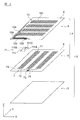
- FIG. 1 is a plan view showing a touch sensor according to an embodiment of the present invention.
- FIG. 2 is an exploded perspective view of the touch sensor.
- FIG. 3 is a cross-sectional view taken along line III-III in FIG.
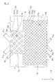
- FIG. 4 is a plan view showing a first wiring body according to an embodiment of the present invention.
- FIG. 5 is a partially enlarged view of a portion V in FIG.
- FIG. 6 is a partially enlarged view of the VI part of FIG.
- FIG. 7 is a diagram for explaining the ratio of the area occupied by the conductor wires.
- 8 is a cross-sectional view taken along line VIII-VIII in FIG.
- FIG. 9 is a cross-sectional view for explaining a first conductor wire according to an embodiment of the present invention.
- FIGS. 1 is a plan view showing a touch sensor according to an embodiment of the present invention.
- FIG. 2 is an exploded perspective view of the touch sensor.
- FIG. 3 is a cross-sectional view
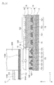
- FIGS. 10A to 10E are cross-sectional views (No. 1) for explaining the method of manufacturing the wiring board according to the embodiment of the invention.
- FIGS. 11A to 11E are cross-sectional views (part 2) for explaining the method of manufacturing the wiring board according to the embodiment of the invention.
- FIG. 12 is a sectional view (No. 3) for explaining the method of manufacturing the wiring board according to the embodiment of the invention.
- FIG. 13 is a cross-sectional view (No. 4) for explaining the method of manufacturing the wiring board according to the embodiment of the invention.
- FIG. 1 is a plan view showing a touch sensor according to an embodiment of the present invention
- FIG. 2 is an exploded perspective view of the touch sensor
- FIG. 3 is a cross-sectional view taken along line III-III in FIG.
- the touch sensor 1 including the wiring board 2 of the present embodiment is a projected capacitive touch panel sensor.
- the touch position is set in combination with a display device (not shown) or the like. It is used as an input device having a detection function.
- the display device is not particularly limited, and a liquid crystal display, an organic EL display, electronic paper, or the like can be used.
- a detection electrode and a drive electrode are arranged so as to overlap with an image displayed on the display device, and between the two electrodes 71 and 101.
- a predetermined voltage is periodically applied from an external circuit (not shown).
- a touch sensor 1 for example, when an operator's finger (external conductor) approaches the touch sensor 1, a capacitor (electrical capacity) is formed between the external conductor and the touch sensor 1, and between the two electrodes. The electrical state of the changes.
- the touch sensor 1 can detect the operation position of the operator based on an electrical change between the two electrodes.
- the “touch sensor 1” in the present embodiment corresponds to an example of the “touch sensor” in the present invention
- the “wiring board 2” in the present embodiment corresponds to an example of the “wiring board” in the present invention.
- the wiring board 2 includes a support body 3 and a wiring body assembly 4 as shown in FIGS.
- the wiring body assembly 4 includes a first wiring body 5, a second wiring body 8 provided on the first wiring body 5, and a connection wiring body 11.
- the support body 3 and the first and second wiring bodies 5 and 8 of the present embodiment are configured to have transparency (translucency) as a whole in order to ensure the visibility of the display device.
- the “wiring body assembly 4” in the present embodiment corresponds to an example of the “wiring body assembly” in the present invention, and the “first wiring body 5” and the “second wiring body 8” in the present embodiment are in the present invention. It corresponds to an example of “wiring body”, and “connection wiring body 11” in the present embodiment corresponds to an example of “connection wiring body” in the present invention.
- the support 3 is a transparent plate-like base material that transmits visible light and supports the first wiring body 5.
- the material constituting the support 3 is polyethylene terephthalate (PET), polyethylene naphthalate (PEN), polyimide resin (PI), polyetherimide resin (PEI), polycarbonate (PC), polyetheretherketone (PEEK). Examples thereof include liquid crystal polymer (LCP), cycloolefin polymer (COP), silicone resin (SI), acrylic resin, phenol resin, epoxy resin, and glass.
- An easy adhesion layer and an optical adjustment layer may be formed on the support 3.
- the “support 3” in the present embodiment corresponds to an example of the “support” in the present invention.
- the first wiring body 5 includes a first resin portion 6 formed in a rectangular shape and a first conductor portion 7 provided on the first resin portion 6.
- the “first resin portion 6” in the present embodiment corresponds to an example of the “resin portion” in the present invention
- the “first conductor portion 7” in the present embodiment corresponds to an example of the “conductor portion” in the present invention. To do.
- the first resin portion 6 is provided to hold the first conductor portion 7.
- the thickness of the first resin portion 6 is preferably 10 ⁇ m to 200 ⁇ m, for example.
- Such a first resin portion 6 includes, for example, an epoxy resin, an acrylic resin, a polyester resin, a urethane resin, a vinyl resin, a silicone resin, a phenol resin, a polyimide resin, and other UV curable resins, thermosetting resins, and thermoplastic resins. It is made of an insulating material such as resin.
- the first conductor portion 7 includes a plurality of first electrodes 71, a plurality of first lead wires 72, a plurality of first terminals 73, a plurality of first boundary portions 74, and a plurality of second electrodes.
- the boundary part 75 of this is included.
- the 1st resin part 6 the 1st electrode 71 and the 1st extraction wiring 72 are integrally formed.
- a first lead wiring 72 and a first terminal 73 are integrally formed. That is, the first electrode 71, the first lead wiring 72, the first terminal 73, the first boundary portion 74, and the second boundary portion 75 are integrally formed.
- integral means that the members are not separated from each other and are formed as an integral structure of the same material (conductive particles, binder resin, etc. having the same particle diameter).
- the “first electrode 71” in the present embodiment corresponds to an example of the “electrode” in the present invention
- the “first lead wiring 72” in the present embodiment corresponds to an example of the “leading wiring” in the present invention
- the “first terminal 73” in the present embodiment corresponds to an example of the “first terminal” in the present invention
- the “second boundary portion 75” in the present embodiment corresponds to an example of the “boundary portion” in the present invention. Equivalent to.
- Each of the first electrodes 71 extends in the Y direction in the drawing, and the plurality of first electrodes 71 are arranged in parallel in the X direction in the drawing.
- a first lead wire 72 is electrically connected to one end in the longitudinal direction of each first electrode 71 via a first boundary portion 74.
- Each first lead wiring 72 extends from one longitudinal end of each first electrode 71 to the vicinity of the outer edge of the first wiring body 5.
- a first terminal 73 is electrically connected to the other end of each first lead wiring 72 through a second boundary portion 75. The first terminal 73 is electrically connected to the connection wiring body 11.
- the number of the 1st electrodes 71 which the 1st wiring body 5 has is not specifically limited, It can set arbitrarily. Further, the number of first lead wires 72 and first terminals 73 included in the first wiring body 5 is set according to the number of first electrodes 71.
- Such a first conductor portion 7 is composed of a binder resin and conductive particles (conductive powder) dispersed in the binder resin.
- Conductive particles include silver, copper, nickel, tin, bismuth, zinc, indium, palladium and other metal materials, graphite, carbon black (furnace black, acetylene black, ketjen black), carbon nanotubes, carbon nanofibers, etc. Can be mentioned. In addition, it may replace with electroconductive particle and may use the metal salt which is a salt of the above-mentioned metal material.
- the conductive particles contained in the first conductor portion 7 may be, for example, a particle diameter ⁇ of 0.5 ⁇ m or more and 2 ⁇ m or less (0.5 ⁇ m ⁇ ⁇ depending on the width of the conductor wire constituting the first conductor portion 7. Conductive particles having ⁇ 2 ⁇ m) can be used. From the viewpoint of stabilizing the electric resistance value in the first conductor portion 7, it is preferable to use conductive particles having an average particle diameter ⁇ that is not more than half the width of the conductor wire constituting the first conductor portion 7. Further, as the conductive particles, it is preferable to use particles having a specific surface area measured by the BET method of 20 m 2 / g or more.
- the first conductor part 7 When a relatively small electrical resistance value of a certain value or less is required as the first conductor part 7, it is preferable to use a metal material as the conductive particles, but as the first conductor part 7, a relatively large value of a certain value or more. When the electrical resistance value is allowed, a carbon-based material can be used as the conductive particles. In addition, it is preferable to use a carbon-based material as the conductive particles from the viewpoint of improving the haze and total light reflectance of the mesh film.
- the first electrode 71 is made to have a mesh shape to impart light transparency to the first electrode 71.
- a conductive material such as silver, copper, nickel, or the above-described carbon-based material that is excellent in conductivity but opaque (such as an opaque metal material and an opaque metal material). Carbon-based material) can be used.
- binder resin examples include acrylic resin, polyester resin, epoxy resin, vinyl resin, urethane resin, phenol resin, polyimide resin, silicone resin, and fluorine resin.
- Such a first conductor portion 7 is formed by applying and hardening a conductive paste.
- the conductive paste include a conductive paste configured by mixing conductive particles, a binder resin, water or a solvent, and various additives.
- the solvent contained in the conductive paste include ⁇ -terpineol, butyl carbitol acetate, butyl carbitol, 1-decanol, butyl cellosolve, diethylene glycol monoethyl ether acetate, and tetradecane.
- the second wiring body 8 includes a second resin portion 9 formed in a rectangular shape and a second conductor portion 10 provided on the second resin portion 9. And.
- the second resin portion 9 is provided so as to cover the first conductor portion 7 and is interposed between the first and second conductor portions 7 and 10.
- the second resin portion 9 functions as a dielectric that exists between the two electrodes 71 and 101 in the touch sensor 1.
- the detection sensitivity of the touch sensor 1 is adjusted by adjusting the thickness of the second resin portion 9.
- the thickness of the second resin portion 9 is preferably 20 ⁇ m to 200 ⁇ m, for example.
- the first terminal 73 is exposed from the notch formed on one side of the second resin portion 9.
- As a material constituting the second resin part 9 the same material as that constituting the first resin part 6 is used.
- the second conductor portion 10 includes a plurality of second electrodes 101, a plurality of second lead wires 102, a plurality of second terminals 103, a plurality of third boundary portions 104, and a plurality of fourth terminals.
- the boundary part 105 is included.
- the second electrode 101 and the second lead wiring 102 are integrally formed.
- the second lead wiring 102 and the second terminal 103 are integrally formed. That is, the second electrode 101, the second lead wiring 102, the second terminal 103, the third boundary portion 104, and the fourth boundary portion 105 are integrally formed.
- Each of the second electrodes 101 extends in the X direction in the drawing, and the plurality of second electrodes 101 are arranged in parallel in the Y direction in the drawing.
- a second lead wire 102 is electrically connected to one end in the longitudinal direction of each second electrode 101 via a third boundary portion 104. Each second lead wire 102 extends from one end in the longitudinal direction of each second electrode 101 to the vicinity of the outer edge of the second wiring body 8.
- a second terminal 103 is electrically connected to the other end of each second lead wiring 102 via a fourth boundary portion 105. The second terminal 103 is electrically connected to the connection wiring body 11.
- the number of the 2nd electrodes 101 which the 2nd wiring body 8 has is not specifically limited, It can set arbitrarily. Further, the number of second lead wires 102 and second terminals 103 included in the second wiring body 8 is set in accordance with the number of second electrodes 101.
- the “second electrode 101” in the present embodiment corresponds to an example of the “electrode” in the present invention
- the “second lead wiring 102” in the present embodiment corresponds to an example of the “leading wiring” in the present invention.
- the “second terminal 103” in the present embodiment corresponds to an example of the “first terminal” in the present invention
- the “fourth boundary portion 105” in the present embodiment corresponds to an example of the “boundary portion” in the present invention. Equivalent to.
- the connection wiring body 11 is an FPC, and includes a strip-shaped base material 111, a plurality of wirings 112 and a plurality of wirings 113 formed on the lower surface of the base material 111.
- the substrate 111 can be made of, for example, a film material made of polyethylene terephthalate (PET), polyethylene naphthalate (PEN), polyimide resin (PI), polyetherimide resin (PEI), or the like.
- PET polyethylene terephthalate
- PEN polyethylene naphthalate
- PI polyimide resin
- PEI polyetherimide resin
- the “base material 111” in the present embodiment corresponds to an example of the “base material” in the present invention.
- a slit 111C is formed at the center in the width direction at one end in the longitudinal direction of the substrate 111, and one end in the longitudinal direction of the substrate 111 is divided into two in the width direction by the slit 111C.
- One end of a plurality of wirings 112 is arranged on the lower surface of one side (first branch portion 111A) of one end in the longitudinal direction of the base material 111, and the other side (second branch portion 111B) of one end in the longitudinal direction of the base material 111. ) Is provided with one end of a plurality of wirings 113.
- connection terminals 112 are parallel to each other as shown in FIG.
- connection terminals 112a are arranged corresponding to the plurality of first terminals 73 of the first wiring body 5, respectively.
- the plurality of wirings 113 are parallel to each other.
- connection terminals 113 a are respectively arranged corresponding to the second terminals 103 of the second wiring body 8.
- the material constituting the wirings 112 and 113 and the connection terminals 112a and 113a is not particularly limited, and copper or the same material as the first conductor portion 7 may be used.
- the “connection terminal 112a” and the “connection terminal 113a” in the present embodiment correspond to an example of the “second terminal” in the present invention.
- connection wiring body 11 is not limited to FPC, For example, it is good also as other wiring boards, such as a rigid board
- the tip of the first branch portion 111A and the region exposed from the notch of the second resin portion 9 in the first wiring body 5 are opposed to each other up and down via the conductive adhesive portion 12. Bonded by the adhesive bonding portion 12. Further, the connection terminal 112 a and the first terminal 73 face each other up and down via the conductive adhesive portion 12.
- the conductive adhesive portion 12 has a function of electrically and mechanically connecting the connection terminal 112a and the first terminal 73 to each other. Further, the conductive adhesive portion 12 has a function of insulating terminals adjacent to each other. Examples of the conductive adhesive portion 12 include an anisotropic conductive film (Anisotropic Conductive Film, ACF), an anisotropic conductive paste (Anisotropic Conductive Paste, ACP), and the like.
- ACF anisotropic Conductive Film
- ACP anisotropic Conductive Paste
- the conductive adhesive portion 12 is configured by dispersing a plurality of terminal conductive particles 122 in a resin material 121.
- a resin material 121 In FIG. 3, four terminal conductive particles 122 dispersed in the resin material 121 are illustrated. However, in the actual conductive adhesive portion 12, a plurality of terminal conductive particles 122 are further included in the resin material. 121 is dispersed.
- the diameter D of the terminal conductive particles 122 (the diameter D of the terminal conductive particles 122), from the viewpoint of improving the connection reliability between the first wiring body 5 and the connection wiring body 11, a first description will be given later.
- conductive particles 122 for terminals conductive particles having a diameter D of 3 ⁇ m to 20 ⁇ m can be used.
- model number CP6920F3 (diameter 3 ⁇ m) or model number CP923CM-25AC (diameter 20 ⁇ m) manufactured by Dexerials is used. Can do.
- connection terminal 112a and the first terminal 73 may be electrically and mechanically connected to each other using a metal paste such as a silver paste or a solder paste without using an anisotropic conductive material. In this case, it is necessary to form a plurality of adhesive portions at intervals so that adjacent terminals are insulated from each other.
- the tip of the second branch portion 111B and the region in the vicinity of one side of the second wiring body 8 face each other up and down via the conductive adhesive portion 12, and the conductive adhesive portion 12 similar to the above is used. It is glued. Further, the connection terminal 113 a and the second terminal 103 face each other up and down via the conductive adhesive portion 12, and are electrically and mechanically connected by the conductive adhesive portion 12.
- the “conductive adhesive portion 12” in the present embodiment corresponds to an example of the “conductive adhesive portion” in the present invention
- the “resin material 121” in the present embodiment corresponds to an example of the “resin material” in the present invention
- the “terminal conductive particles 122” in the present embodiment corresponds to an example of “conductive particles” in the present invention.
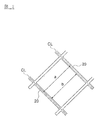
- FIG. 4 is a plan view showing a first wiring body according to an embodiment of the present invention
- FIG. 5 is a partially enlarged view of a V portion in FIG. 4
- FIG. 6 is a partially enlarged view of a VI portion in FIG.
- the first electrode 71 has a mesh shape constituted by a plurality of linear third conductor lines 711. Specifically, as shown in FIG.
- a plurality of third conductor wires 711 a extending in a direction inclined at + 45 ° with respect to the X direction (hereinafter also referred to as “first direction”) direction substantially perpendicular to the first direction (hereinafter, also referred to as a "second direction”.) is arranged in equal pitch P 31, the third conductor wire plurality extending in a second direction 711b have been arranged in equal pitch P 32 in the first direction.
- the third conductor lines 711a and 711b intersect each other at right angles, thereby forming a mesh-like first electrode 71 in which square-shaped (rhombus-shaped) third meshes 715 are repeatedly arranged. Yes.
- the third conductor line 711 is a general term for the third conductor line 711a and the third conductor line 711b.
- a third virtual circle 716 is inscribed in the third mesh 715 of the first electrode 71 in plan view.
- Diameter S 3 of the third virtual circle 716 (diameter S 3 of the third virtual circle 716) can be set in the range of 90 [mu] m ⁇ 500 [mu] m, is preferably 250 ⁇ m or less.
- the virtual circle inscribed in the mesh is the largest virtual true circle inscribed in the mesh in plan view. In this embodiment, it is a virtual perfect circle that is inscribed in each side of the square mesh in plan view.
- each third mesh 715 constituting the mesh shape of the first electrode 71 is not particularly limited to the above.
- it may be a triangle such as a regular triangle, an isosceles triangle, a right triangle, or a quadrangle such as a parallelogram or a trapezoid.
- the mesh shape may be an n-gon such as a hexagon, an octagon, a dodecagon, or an icosahedron, a circle, an ellipse, or a star. In this manner, a geometric pattern obtained by repeating various graphic units can be used as the shape of each mesh of the first electrode 71.
- the width W 3 (maximum width) of the third conductor wire 711 can be set within a range of 0.5 ⁇ m to 10 ⁇ m, and is preferably 5 ⁇ m or less.
- the height of the third conductor wire 711 is preferably 0.5 ⁇ m to 10 ⁇ m.
- the width of the conductor line corresponds to the interval between the meshes adjacent to each other in the direction orthogonal to the extending direction of the conductor line.
- the ratio (W 3 / S 3 ) of the width W 3 and the diameter S 3 is set within a range of 0.001 to 0.12. It is preferably 0.002 to 0.055. Further, from the viewpoint of improving the visibility of the touch sensor 1, the ratio A 3 of the area occupied by the third conductor line 711 in the first electrode 71 be set within a range 0.19% - 19% It is preferably 0.39% to 10.2%.
- the “ratio of the area occupied by the conductor wire” in the mesh shape means a ratio represented by the following expression (12) (see FIG. 7).
- (Ratio of area occupied by conductor wire) ⁇ (a ⁇ a) ⁇ (b ⁇ b) ⁇ / (a ⁇ a) (12)
- a is a pitch (a distance between the center lines CL) between an arbitrary conductor line 20 and another conductor line 20 adjacent to the conductor line 20
- b is an arbitrary The distance between the conductor line 20 and another conductor line 20 adjacent to the conductor line 20 is represented.
- the “third conductor line 711” in the present embodiment corresponds to an example of the “third conductor line” in the present invention
- the “third mesh 715” in the present embodiment is the “third mesh” in the present invention
- the “third virtual circle 716” in the present embodiment corresponds to an example of the “third virtual circle” in the present invention.
- the first lead-out wiring 72 has a mesh shape constituted by a plurality of linear first conductor lines 721. Specifically, as shown in FIG. 5, a plurality of first conductor line 721a extending in a first direction are arranged in equal pitch P 11 in a second direction, extending in the second direction a plurality of first conductor lines 721b are arranged at equal pitches P 12 in the first direction.
- the first conductor lines 721a and 721b intersect each other at right angles, thereby forming a mesh-like first lead-out wiring 72 in which square-shaped (rhombus-shaped) first meshes 725 are repeatedly arranged.
- the first conductor line 721 is a general term for the first conductor line 721a and the first conductor line 721b.
- the shape of the first mesh 725 a geometric pattern obtained by repeating various graphic units can be used as in the shape of the third mesh 715.
- the plurality of first meshes 725 are regularly arranged in the entire first lead-out wiring 72, but the present invention is not particularly limited thereto.
- a part of the first lead wiring 72 there may be a portion where the plurality of first meshes 725 are not regularly arranged.
- the first mesh 725 is divided into two equal parts along the extending direction of the first lead wiring 72 at the end in the width direction of the first lead wiring 72.
- the defect portion may be filled with a conductor portion.
- the first virtual circle 726 is inscribed in the first mesh 725 of the first lead wiring 72 in a plan view.
- the diameter S 1 of the first virtual circle 726 can be set within a range of 3 ⁇ m to 50 ⁇ m, and is preferably 10 ⁇ m or less.
- the width W 1 (maximum width) of the first conductor wire 721 can be set within a range of 5 ⁇ m to 200 ⁇ m, and is preferably 10 ⁇ m or more.
- the height of the first conductor wire 721 is preferably 0.5 ⁇ m to 20 ⁇ m.
- the ratio of the width W 1 to the diameter S 1 is in the range of 0.10 to 66 from the viewpoint of improving the conductivity and improving the detection sensitivity of the touch sensor. 1 to 66, and preferably 1 to 66.
- the ratio A 1 of the area occupied by the first conductor line 721 in the first lead line 72 can be set in the range of 17% to 99.9%, and 75% to 99.9% It is preferable.
- the “first conductor line 721” in the present embodiment corresponds to an example of the “first conductor line” in the present invention
- the “first mesh 725” in the present embodiment is the “first mesh” in the present invention
- the “first virtual circle 726” in the present embodiment corresponds to an example of the “first virtual circle” in the present invention.
- the first boundary portion 74 interposed between the first electrode 71 and the first lead wiring 72 is configured by a single linear conductor line.
- the first boundary portion 74 ensures that the first electrode 71 and the first lead wire 72 are connected to each other when the mesh shape of the first electrode 71 and the mesh shape of the first lead wire 72 are different.
- the length of the first boundary portion 74 in the longitudinal direction (in the present embodiment, the X direction in the drawing) is set to be equal to or larger than the width of the first lead wiring 72 and equal to or smaller than the width of the first electrode 71. ing.
- the first boundary portion 74 is connected to the third conductor wire 711 located at one end in the longitudinal direction of the first electrode 71, and the first conductor wire 721 located at one end of the first lead-out wiring 72 It is connected.
- the width of the first boundary portion 74 is preferably 10 ⁇ m to 100 ⁇ m.
- the 1st boundary part 74 may be comprised not only by the linear conductor wire but the curved conductor wire.
- the first terminal 73 has a mesh shape constituted by a plurality of linear second conductor lines 731. Specifically, a plurality of second conductor lines 731a extending in a first direction are arranged in equal pitch P 21 in the second direction, the second conductor lines of a plurality extending in a second direction 731b are arranged at equal pitches P 22 in the first direction. Then, the second conductor lines 731a and 731b intersect perpendicularly to each other, thereby forming a mesh-shaped first terminal 73 in which square-shaped (rhombus-shaped) second mesh 735 is repeatedly arranged. Yes.
- the second conductor line 731 is a general term for the second conductor line 731a and the second conductor line 731b.
- the shape of the second mesh 735 a geometric pattern obtained by repeating various graphic units can be used as in the shape of the third mesh 715.
- the plurality of second meshes 735 are regularly arranged in the entire first terminal 73, but the present invention is not particularly limited thereto.
- a portion where the plurality of second meshes 735 are not regularly arranged For example, in FIG. 6, at the end in the width direction of the first terminal 73, a missing portion having a shape obtained by dividing the quadrangular shape into two equal parts along the extending direction of the first terminal 73 as the second mesh 735.
- this missing portion may be filled with a conductor portion.
- a second virtual circle 736 is inscribed in the second mesh 735 of the first terminal 73 in plan view.
- the diameter S 2 of the second virtual circle 736 and the first mesh of the first lead-out wiring 72 satisfies the relationship of the following expression (14). S 2 ⁇ S 1 (14)
- Such diameter S 2 can be set in the range of 3 [mu] m ⁇ 30 [mu] m, is preferably 10 ⁇ m or less.
- the width W 2 (maximum width) of the second conductor wire 731 and the first conductor constituting the first lead-out wiring 72.
- the width W 1 of the line 721 it is preferable to satisfy the following relationship (15).
- the width W 2 (maximum width) of the second conductor wire 731 can be set within a range of 3 ⁇ m to 50 ⁇ m, and is preferably 10 ⁇ m or less.
- the height of the second conductor wire 731 is preferably 0.5 ⁇ m to 20 ⁇ m.
- the ratio of the width W 2 and the diameter S 2 (W 2 / S 2 ), the width W 1 and the diameter S 1 of the ratio (W 1 / S 2) and is preferably satisfy the following relationship (17).
- the ratio of the width W 2 to the diameter S 2 (W 2 / S 2 ) and the ratio of the width W 3 to the diameter S 3 (W 3 / S 3 ) are: It is preferable that the relationship of the following formula (18) is satisfied. W 3 / S 3 ⁇ W 2 / S 2 (18)
- the ratio (W 2 / S 2 ) between the width W 2 and the diameter S 2 can be set within a range of 0.10 to 17, and is 0.3 to 3.4. Is preferred.
- the electroconductive particle 122 for terminals is efficiently stayed between the 1st terminal 73 and the connection terminal 112a, and the 1st wiring body 5, the connection wiring body 11, and From the viewpoint of improving the connection reliability, the ratio of the width W 2 to the diameter S 2 (W 2 / S 2 ) is preferably 0.5 or less.
- the ratio (W 2 / S 2 ) between the width W 2 and the diameter S 2 is preferably 1 or less.
- the ratio A 2 and the ratio A 3 of the area occupied by the third conductor wire 711 in the first electrode 71 satisfy the relationship of the following expression (20). It is preferable. A 3 ⁇ A 2 (20)
- Such a ratio A 2 can be set in the range of 17% to 99.6%, preferably 40% to 94.7%. Further, when the conductive adhesive portion 12 is used, the contact area between the first terminal 73 and the connection terminal 112a via the conductive adhesive portion 12 is increased, so that the first wiring body 5 and the connection wiring body 11 are connected. From the viewpoint of improving connection reliability, the ratio A 2 is preferably 75% or less, and the terminal conductive particles 122 are efficiently retained between the first terminal 73 and the connection terminal 112a. From the viewpoint of improving the connection reliability between the first wiring body 5 and the connection wiring body 11, the ratio a 2 is more preferably 56% or less. That is, the ratio A 2 is 40% ⁇ 75%, even more preferably from 40% to 56%.
- the “second conductor wire 731” in the present embodiment corresponds to an example of the “second conductor wire” in the present invention
- the “second mesh 735” in the present embodiment is the “second mesh” in the present invention
- the “second virtual circle 736” in the present embodiment corresponds to an example of the “second virtual circle” in the present invention.
- the second boundary portion 75 interposed between the first lead-out wiring 72 and the first terminal 73 is composed of a single linear conductor line.
- the second boundary portion 75 reliably connects the first lead wire 72 and the first terminal 73 when the mesh shape of the first lead wire 72 and the mesh shape of the first terminal are different. To be provided.
- the length of the second boundary portion 75 in the longitudinal direction is the smaller one of the width of the first lead-out wiring 72 and the width of the first terminal 73 (this In the embodiment, the width is equal to or greater than the width of the first lead-out wiring 72, and the width on the larger side of the width of the first lead-out wiring 72 and the width of the first terminal 73 (in this embodiment, the first lead-out wiring 72 is the first width).
- the second boundary portion 75 is connected to the first conductor line 721 located at the other end of the first lead wire 72 and connected to the second conductor line 731 located at one end of the first terminal 73.
- the width of the second boundary portion 75 is preferably 10 ⁇ m to 100 ⁇ m.
- the 2nd boundary part 75 may be comprised not only with the linear conductor wire but with the curved conductor wire.
- the second electrode 101 has a mesh shape composed of a plurality of linear conductor lines. Similar to the first lead-out line 72, the second lead-out line 102 has a mesh shape composed of a plurality of linear conductor lines. The third boundary portion 104 interposed between the second electrode 101 and the second lead wiring 102 is configured by a single conductor line. Similar to the first terminal 73, the second terminal 103 has a mesh shape composed of a plurality of linear conductor wires. The fourth boundary portion 105 interposed between the second lead wiring 102 and the second terminal 103 is configured by a single conductor line.
- the basic configuration of the second electrode 101 is the same as that of the first electrode 71.
- the basic configuration of the second lead wiring 102 is the same as that of the first lead wiring 72.
- the basic configuration of the second terminal 103 is the same as that of the first terminal 73.
- the basic configuration of the third boundary portion 104 is the same as that of the first boundary portion 74.
- the basic configuration of the fourth boundary portion 105 is the same as that of the second boundary portion 75.
- the second electrode 101, the second lead wiring 102, the second terminal 103, the third boundary portion 104, and the fourth boundary portion 105 are referred to as the first electrode 71, the first electrode
- the description of the lead wiring 72, the first terminal 73, the first boundary portion 74, and the second boundary portion 75 is incorporated and detailed description is omitted.
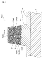
- FIG. 8 is a cross-sectional view taken along line VIII-VIII in FIG. 5, and FIG. 9 is a cross-sectional view for explaining a first conductor line according to an embodiment of the present invention.
- 8 and 9 the first resin part 6 and the first conductor part 7 constituting the first wiring body 5 of the present embodiment will be described in an easy-to-understand manner. The illustration of the configuration is omitted.
- the first resin portion 6 has a flat portion 61 and a protruding portion 62.
- the flat portion 61 is a portion formed in a layer shape in the first resin portion 6.
- the upper surface of the flat portion 61 is a substantially flat surface.
- the protruding portion 62 protrudes toward the side away from the flat portion 61 and is formed integrally with the flat portion 61 on the flat portion 61.
- the projecting portion 62 is provided corresponding to the first conductor wire 721 and supports the first conductor wire 721.
- the protrusion 62 has a resin part contact surface 621 that contacts a first conductor wire 721 (specifically, a conductor part contact surface 722 (described later)). As shown in FIG. 8, the resin portion contact surface 621 has an uneven shape that is complementary to the conductor portion contact surface 722 having an uneven shape. Although not particularly illustrated, the resin part contact surface 621 and the conductor part contact surface 722 also have a concavo-convex shape that is complementary to each other in the cross section in the extending direction of the first conductor wire 721. In FIG. 8, the concave and convex shapes of the resin portion contact surface 621 and the conductor portion contact surface 722 are exaggerated for easy understanding of the first wiring body 5 of the present embodiment.
- the first conductor wire 721 When the cross section in the width direction of the first conductor wire 721 is viewed, the first conductor wire 721 includes a conductor portion contact surface 722, a conductor portion top surface 723, a conductor portion side surface 724, as shown in FIG. have.
- the conductor portion contact surface 722 is a surface that is in contact with the resin portion contact surface 621.
- the conductor portion contact surface 722 has an uneven shape. This uneven shape is formed based on the surface roughness of the conductor contact surface 722. The surface roughness of the conductor contact surface 722 will be described in detail later.
- the conductor portion top surface 723 is a surface opposite to the conductor portion contact surface 722 in the first conductor portion 7.
- the conductor portion top surface 723 in the present embodiment includes a straight top surface flat portion 7231. In the cross section in the width direction of the first conductor portion 7, the width of the top flat portion 7231 is at least half the width of the conductor top surface 723. In this embodiment, substantially the entire conductor portion top surface 723 is a top surface flat portion 7231.
- the flatness of the top flat portion 7231 is 0.5 ⁇ m or less. The flatness can be defined by the JIS method (JIS B0621 (1984)).
- the flatness of the top flat portion 7231 is obtained using a non-contact measurement method using laser light.
- the measurement target is irradiated with a belt-shaped laser beam, and the reflected light is imaged on an image sensor (for example, a two-dimensional CMOS) to measure the flatness.
- an image sensor for example, a two-dimensional CMOS
- a method for calculating the flatness a method (maximum deflection flatness) is used in which a plane passing through three points as far apart as possible is set in the target plane, and the maximum value of the deviation is calculated as the flatness.
- the flatness measurement method and calculation method are not particularly limited to those described above.
- the flatness measurement method may be a contact-type measurement method using a dial gauge or the like.
- a method of calculating a value of a gap formed when a target plane is sandwiched between parallel planes as the flatness (maximum inclination flatness) may be used.
- the conductor part side surface 724 is interposed between the conductor part contact surface 722 and the conductor part top surface 723.
- the conductor portion side surface 724 is connected to the conductor portion top surface 723 at one end portion 7241 and is connected to the conductor portion contact surface 722 at the other end portion 7242.
- the conductor portion side surface 724 and the side surface of the protruding portion 62 are continuously connected.
- the two conductor side surfaces 724 and 724 in one first conductor portion 7 are inclined so as to approach the center of the first conductor wire 721 as the distance from the first resin portion 6 increases.
- the first conductor line 721 has a tapered shape that becomes narrower as the distance from the first resin portion 6 increases in the cross section in the width direction of the first conductor line 721.
- the conductor portion side surface 724 includes a side surface flat portion 7243 in the cross section in the width direction of the first conductor wire 721.
- the side flat portion 7243 is a linear portion existing on the conductor side surface 724 in the cross section in the width direction of the first conductor wire 721.
- the flatness of the side flat portion 7243 is 0.5 ⁇ m or less.
- the conductor portion side surface 724 of the present embodiment is a surface extending on an imaginary straight line (not shown) passing through both ends 7241 and 7242 thereof. In this case, the substantially entire conductor side surface 724 is a side flat portion 7243.
- the shape of the conductor portion side surface 724 is not particularly limited to the above.
- the conductor side surface 724 may have an arc shape that protrudes outward in the cross section in the width direction of the first conductor wire 721.
- the conductor part side surface 724 exists outside the virtual straight line passing through both ends 7241 and 7242 of the conductor part side surface 724.
- the conductor side surface 724 has a shape that does not exist on the inner side of the imaginary straight line passing through both ends in the cross section in the width direction of the conductor.
- the conductor side surface in the cross section in the width direction of the conductor wire, when the width of the conductor wire gradually increases as it approaches the first resin portion, the conductor side surface faces inward. It is preferably not a concave arc shape (that is, a shape in which the bottom of the conductor wire is widened).
- the angle ⁇ of the corner between the conductor side surface 724 and the conductor top surface 723 is 90 ° to 170 ° (90 ° ⁇ ⁇ ⁇ 170 °). It is preferably 90 ° to 120 ° (90 ° ⁇ ⁇ ⁇ 120 °).
- the angle between one conductor portion side surface 724 and the conductor portion top surface 723, and the angle between the other conductor portion side surface 724 and the conductor portion top surface 723, Are substantially the same.
- the surface roughness of the conductor portion contact surface 722 is relatively large with respect to the surface roughness of the conductor portion top surface 723.
- the conductor portion top surface 723 includes the top surface flat portion 7231, the relative relationship of the first surface roughness (the conductor portion top surface with respect to the surface roughness of the conductor portion contact surface 722).
- the relation that the surface roughness of the surface 723 is relatively large) is established.
- the surface roughness Ra of the conductor contact surface 722 is 0.1 ⁇ m to 3 ⁇ m
- the surface roughness Ra of the conductor top surface 723 is 0.001 ⁇ m to 1.0 ⁇ m. It is preferable.
- the surface roughness Ra of the conductor contact surface 722 is more preferably 0.1 ⁇ m to 0.5 ⁇ m, and the surface roughness Ra of the conductor top surface 723 is 0.001 ⁇ m to 0.3 ⁇ m. More preferred.
- the relationship of the surface roughness of the conductor top surface 723 to the surface roughness of the conductor contact surface 722 is preferably 0.01 to less than 1, more preferably 0.1 to less than 1.
- the surface roughness of the conductor top surface 723 is preferably 1/5 or less of the width (maximum width) of the first conductor wire 721. Such surface roughness can be measured by the JIS method (JIS B0601 (revised on March 21, 2013)).
- the surface roughness of the conductor contact surface 722 and the surface roughness of the conductor top surface 723 may be measured along the width direction of the first conductor wire 721 or the extending direction of the first conductor wire 721. You may go along.
- surface roughness Ra here means “arithmetic average roughness Ra”.
- the “arithmetic average roughness Ra” refers to a roughness parameter obtained by blocking a long wavelength component (swell component) from a cross-sectional curve. Separation of the waviness component from the cross-sectional curve is performed based on measurement conditions (for example, dimensions of the object) necessary for obtaining the shape.
- the conductor side surface 724 also includes a side flat portion 7243.
- the surface roughness of the conductor contact surface 722 is relatively larger than the surface roughness of the conductor side surface 724.
- the surface roughness Ra of the conductor portion side surface 724 is preferably 0.001 ⁇ m to 1.0 ⁇ m, whereas the surface roughness Ra of the conductor portion contact surface 722 is 0.1 ⁇ m to 3 ⁇ m. More preferably, it is 001 ⁇ m to 0.3 ⁇ m.
- the surface roughness of the conductor side surface 724 may be measured along the width direction of the first conductor wire 721 or along the extending direction of the first conductor wire 721.
- the conductor portion The diffuse reflectance on the other surface side other than the conductor contact surface 722 is smaller than the diffuse reflectance on the contact surface 722 side.
- the ratio of the diffuse reflectance on the conductor portion contact surface 722 side to the diffuse reflectance on the other surface side other than the conductor portion contact surface 722 is preferably less than 0.1 to 1, preferably 0.3 to 1. More preferably, it is less.
- the conductor portion contact surface 722B of the first conductor portion 7B constituted by the conductive particles M and the binder resin B, a part of the conductive particles M is binder resin in the cross section in the width direction of the first conductor portion 7B. Projects from B. Thereby, the conductor portion contact surface 722B has an uneven shape.
- the binder resin B enters between the conductive particles M in the cross section in the width direction of the first conductor portion 7B.
- the conductor portion top surface 723B and the conductor portion side surface 724B cover the conductive particles M. Accordingly, the conductor top surface 723B includes a straight top flat portion 7231B, and the conductor side surface 724B includes a straight side flat portion 7243B.
- the surface roughness of the conductor portion contact surface 722B is relatively large with respect to the surface roughness of the conductor portion top surface 723B and is relatively large with respect to the surface roughness of the conductor portion side surface 724B.
- the binder resin B covers the conductive particles M on the conductor side surface 724B, the electrical insulation between the adjacent first conductor parts 7B is improved, and the occurrence of migration is suppressed.
- the third conductor wire 711 constituting the first electrode 71 has the same basic configuration as the first conductor wire 721 described above. Therefore, in this specification, the repeated description of the third conductor wire 711 is omitted, and the description of the first conductor wire 721 is used.
- the second conductor wire 731 constituting the first terminal 73 has the same basic configuration as the first conductor wire 721 described above. Therefore, in the present specification, the repeated description of the second conductor wire 731 is omitted, and the description of the first conductor wire 721 is incorporated.
- the conductor lines constituting the first and second boundary portions 74 and 75 have the same basic configuration as the first conductor line 721 described above. Therefore, in the present specification, the description of the first conductor wire 721 will be incorporated by omitting repeated description of the conductor wires constituting the first and second boundary portions 74 and 75.
- FIG. 10A to FIG. 10E, FIG. 11A to FIG. 11E, FIG. 12 and FIG. 13 are for explaining a method of manufacturing a wiring board according to an embodiment of the present invention.
- FIG. 10A to FIG. 10E, FIG. 11A to FIG. 11E, FIG. 12 and FIG. 13 are for explaining a method of manufacturing a wiring board according to an embodiment of the present invention.
- FIG. 10A to FIG. 10E, FIG. 11A to FIG. 11E, FIG. 12 and FIG. 13 are for explaining a method of manufacturing a wiring board according to an embodiment of the present invention.
- a first conductive material 210 is filled into a first intaglio plate 200 in which a first recess 201 having a shape corresponding to the shape of the first conductor portion 7 is formed.
- the first conductive material 210 filled in the first recess 201 of the first intaglio 200 the above-described conductive paste is used.
- the material constituting the first intaglio 200 include glass such as silicon, nickel, and silicon dioxide, ceramics, organic silica, glassy carbon, thermoplastic resin, and photocurable resin.
- a release layer (not shown) made of a graphite material, a silicone material, a fluorine material, a ceramic material, an aluminum material, or the like is provided on the surface of the first recess 201 in order to improve releasability. It is preferable to form it in advance.
- Examples of the method of filling the first conductive material 210 into the first concave portion 201 of the first intaglio 200 include a dispensing method, an inkjet method, and a screen printing method.
- the first conductive material 210 applied to the portion other than the first concave portion 201 is wiped off. Or the method of scraping, blotting, sticking, washing away, and blowing off can be mentioned.
- the first conductive material 210 can be appropriately used.
- the first conductive material 210 filled in the first recess 201 is heated and cured.
- the heating condition of the first conductive material 210 can be set as appropriate depending on the composition of the first conductive material 210 and the like.
- volumetric shrinkage occurs in the first conductive material 210 due to the heat treatment.
- the portion of the first conductive material 210 that is in contact with the inner wall surface of the first recess 201 is transferred to the shape of the inner wall surface of the first recess 201 and becomes a flat shape.
- the portion of the first conductive material 210 that does not contact the inner wall surface of the first recess 201 is not affected by the shape of the inner wall surface of the first recess 201. For this reason, a fine uneven
- the method for treating the first conductive material 210 is not particularly limited to heating. Energy rays such as infrared rays, ultraviolet rays, and laser beams may be applied, or only drying may be performed. Moreover, you may combine these 2 or more types of processing methods.
- a first resin material 220 for forming the first resin portion 6 is applied onto the first intaglio 200.
- the resin material which comprises the 1st resin part 6 mentioned above is used.
- the method for applying the first resin material 220 onto the first intaglio 200 include a screen printing method, a spray coating method, a bar coating method, a dip method, and an ink jet method.
- the first resin material 220 enters the first recess 201 into the gap generated by the volume shrinkage of the first conductive material 210 described above.
- the support 3 is disposed on the first intaglio 200, and the first resin material 220 is interposed between the support 3 and the first intaglio 200. Then, the support 3 is pressed against the first intaglio 200. Then, the first resin material 220 is cured.
- the method for curing the first resin material 220 include irradiation with energy rays such as ultraviolet rays and infrared laser beams, heating, heating and cooling, and drying. Thereby, the 1st resin part 6 is formed.
- the formation method of the 1st resin part 6 is not specifically limited above.
- coated the 1st resin material 220 on the support body 3 substantially uniformly is prepared, and the said support body so that the said 1st resin material 220 may enter into the 1st recessed part 201 of the 1st intaglio 200
- the first resin portion 6 may be formed by pressing 3 to the first intaglio 200 and curing the first resin material 220 while maintaining the state.
- the intermediate body 230 including the support body 3, the first conductor portion 7, and the first resin portion 6 is integrally peeled from the first intaglio 200.
- a second intaglio 240 having a second recess 241 corresponding to the shape of the second conductor 10 is prepared.
- a material constituting the second intaglio 240 the same material as that constituting the first intaglio 200 is used.
- a release layer (not shown) may be formed in advance on the surface of the second intaglio 240.
- the second conductive material 250 is filled in the second concave portion 241 of the second intaglio 240 to form the second conductive portion 10, and this is cured.
- the second conductive material 250 the above-described conductive paste is used.
- a method for filling the second recess 241 with the second conductive material 250 a method similar to the method for filling the first recess 201 with the first conductive material 210 is used.
- a method for curing the second conductive material 250 a method similar to the method for curing the first conductive material 210 is used.
- a second resin material 260 is applied on the intermediate body 230 so as to cover the first conductor portion 7 in order to form the second resin portion 9.
- the viscosity of the second resin material 260 is preferably 1 mPa ⁇ s to 10,000 mPa ⁇ s from the viewpoint of securing sufficient fluidity during application.
- the storage elastic modulus of the cured resin is preferably 10 6 Pa or more and 10 9 Pa or less from the viewpoint of durability of the first conductor portion 7 and the second conductor portion 10.
- a method of applying the second resin material 260 a method similar to the method of applying the first resin material 220 is used.
- the intermediate body 230 is disposed on the second intaglio 240, and the second resin material 260 becomes the second recess 241 (specifically, the second intaglio 240). Presses the intermediate body 230 against the second intaglio 240 so as to enter the voids generated by the volume contraction of the second conductive material 250 and hardens it.
- the pressing force when pressing the intermediate body 230 against the second intaglio 240 is preferably 0.001 MPa to 100 MPa, and more preferably 0.01 MPa to 10 MPa.
- the said pressurization can be performed using a pressure roller etc.
- the second resin material 260 As a method of curing the second resin material 260, a method similar to the method of curing the first resin material 220 is used. Thereby, the second resin portion 9 is formed, and the intermediate body 230 and the second conductor portion 10 are bonded and fixed to each other via the second resin portion 9.
- the intermediate body 230, the second resin portion 9, and the second conductor portion 10 are integrally peeled from the second intaglio 240.
- connection terminal 112 a of the wiring 112 of the connection wiring body 11 prepared in advance and the first terminal 73 of the first wiring body 5 are opposed to each other through the conductive adhesive portion 12.
- the connection terminal 113a of the wiring 113 and the second terminal 103 of the second wiring body 8 are disposed to face each other with the conductive adhesive portion 12 interposed therebetween.
- the first and second wiring bodies 5, 8 and the connection wiring body 11 are thermocompression bonded by the thermocompression bonding apparatus 300 through the conductive adhesive portion 12.
- the first and second wiring bodies 5 and 8 and the connection wiring body 11 are connected.
- the wiring board 2 can be obtained.
- the first wiring body 5, the wiring body assembly 4, the wiring board 2, and the touch sensor 1 of the present embodiment have the following effects.
- the first mesh 725 of the first lead-out wiring 72 and the second mesh 735 of the first terminal 73 are set so that the relationship between the diameter S 1 and the diameter S 2 satisfies the above expression (14). It is set. For this reason, the gap of the first mesh 725 of the first lead-out wiring 72 is larger than the gap of the second mesh 735 of the first terminal 73. As a result, the first lead wiring 72 is resistant to elongation, so that the disconnection of the first lead wiring 72 can be prevented.
- the second mesh 735 is densely formed, and an adhesion effect between the first terminal 73 and the connection terminal 112 a can be improved by the action of the anchor effect in the first terminal 73. Thereby, the connection reliability between the first wiring body 5 and the connection wiring body 11 can be improved.
- the relationship between the width W 1 and the width W 2 satisfies the above equation (15).
- the surface area of the first terminal 73 can be set relatively large by continuously arranging the second conductor wires 731 having a relatively small width.
- the action of the anchor effect is further strengthened.
- the adhesive strength with the connection wiring body 11 in the 1st terminal 73 increases, and the adhesive force of the 1st wiring body 5 and the connection wiring body 11 can be improved.
- the connection reliability between the first wiring body 5 and the connection wiring body 11 can be improved.
- the relationship between the width W 1 and the width W 2 satisfies the above equation (15), and the first conductor wire 721 having a relatively large width is used for the first lead wiring 72.
- the electrical resistance value in the first lead wiring 72 can be reduced. Thereby, the detection sensitivity of the touch sensor 1 using the 1st wiring body 5 can be improved.
- the relationship between the ratio of the width W 1 to the diameter S 1 (W 1 / S 1 ) and the ratio of the width W 2 to the diameter S 2 (W 2 / S 2 ) is expressed by the above equation (17).
- the proportion of the area occupied by the conductor wire in the first lead-out wiring 72 is larger than the proportion of the area occupied by the conductor wire in the first terminal 73, and the electric power in the first lead-out wiring 72 is The resistance value can be reduced. Thereby, the detection sensitivity of the touch sensor 1 using the 1st wiring body 5 can be improved.
- the electrical resistance value in the first lead-out wiring 72 is further reduced, and the first wiring body 5 is formed.
- the detection sensitivity of the used touch sensor 1 can be further improved.
- the relationship between the diameter S 1 and the diameter S 3 satisfies the relationship of the equation (13).
- the visibility of the touch sensor 1 using the first wiring body 5 can be improved.
- the relationship between the width W 2 and the width W 3 satisfies the above formula (16).
- the third conductor wire 711 constituting the first electrode 71 is difficult to visually recognize, and light is not easily blocked by the third conductor wire 711 in the first electrode. The visibility of the touch sensor 1 using can be improved.
- the relationship between the ratio of the width W 2 and the diameter S 2 (W 2 / S 2 ) and the ratio of the width W 3 and the diameter S 3 (W 3 / S 3 ) is expressed by the above equation (18).
- filling the ratio of the area which the conductor wire in the 1st electrode 71 occupies can be set small. Thereby, light is easily transmitted through the first electrode 71, and the visibility of the touch sensor 1 using the first wiring body 5 can be improved.
- the relationship between the ratio A 2 and the ratio A 3 satisfies the relationship expressed by the above equation (20), light is less likely to be blocked by the third conductor wire 711 in the first electrode 71. The visibility of the touch sensor 1 using the wiring body 5 can be further improved.
- the second boundary portion is interposed between the first lead-out wiring 72 and the first terminal 73 and electrically connects the first lead-out wiring 72 and the first terminal 73.
- 75 is provided. For this reason, even when the mesh shape of the first lead wire 72 and the mesh shape of the first terminal 73 are different, the first lead wire 72 and the first terminal 73 are more reliably electrically connected. Can do.
- the first terminal 73 of the first wiring body 5 and the connection terminal 112 a of the connection wiring body 11 are bonded by the conductive adhesive portion 12. Then, the relationship between the diameter D and the diameter S 2 of the terminal for the conductive particles 122 contained in the conductive adhesive portion 12 meets the expression (10). In this case, the terminal conductive particles 122 can be prevented from falling into the second mesh 735, and the electrical connection between the first terminal 73 and the connection terminal 112a via the terminal conductive particles 122 can be suppressed. Connection can be made more reliably. Thereby, the connection reliability of the 1st wiring body 5 and the connection wiring body 11 can be improved. Moreover, since the contact resistance between the 1st terminal 73 and the connection terminal 112a can be reduced, the detection sensitivity of the touch sensor 1 using the 1st wiring body 5 can be improved.
- the terminal conductive particles 122 Since it becomes easy to be collected by the second mesh 735 of the first terminal 73, it is possible to suppress the flow between the first wiring body 5 and the connection wiring body 11 from flowing out. Thereby, the electrical connection between the first terminal 73 and the connection terminal 112a can be more reliably performed, and the connection reliability between the first wiring body 5 and the connection wiring body 11 can be improved.
- the second conductor wire 731 has a tapered shape that becomes narrower as the distance from the first resin portion 6 increases in the cross section in the width direction of the second conductor wire 731. For this reason, when the first wiring body 5 and the connection wiring body 11 are thermocompression bonded, the terminal conductive particles 122 are further easily collected by the second mesh 735 of the first terminal 73. It is possible to suppress the flow between the one wiring body 5 and the connection wiring body 11. Thereby, the electrical connection between the first terminal 73 and the connection terminal 112a can be more reliably performed, and the connection reliability between the first wiring body 5 and the connection wiring body 11 can be improved.
- the basic configuration of the second wiring body 8 is the same as that of the first wiring body 5. For this reason, also in the connection structure of the 2nd wiring body 8 and the connection wiring body 11, the effect
- Table 1 shows the ratio between the diameter S 1 ( ⁇ m) of the first virtual circle 726 of the first lead-out wiring 72 and the diameter S 2 ( ⁇ m) of the second virtual circle 736 of the first terminal 73 (S 1 / S 2 ), the evaluation of the elongation (%) when the resistance of the first lead-out wiring 72 is 1.5 times, and the crushing rate (%) of the conductive particles 122 for terminals having a diameter of 10 ⁇ m.
- the relationship with evaluation is shown.
- the diameter S 1 of the first temporary circle 726 ( ⁇ m), and the diameter S 2 of the second imaginary circle 736 ([mu] m) is adjusted in the range of 5 ⁇ 15 [mu] m.
- the above-described elongation rate is the elongation rate of the first lead wire 72 when the resistance value of the first lead wire 72 increases 1.5 times before and after applying tension to the first lead wire 72. It is. Here, when the resistance value increases 1.5 times, it is considered that the first lead wiring 72 is broken.
- the crushing rate of the terminal conductive particles 122 is the ratio of the minimum diameter after use to the diameter before use.
- the elongation ratio of the first lead-out wiring 72 is evaluated in three stages: “excellent” (double circle in the table), “good” (circle in the table), and “impossible” (cross in the table). Went.
- the crushing rate of the terminal conductive particles 122 was evaluated in two stages, “good” (circle in the table) and “impossible” (cross in the table).
- “excellent” the strength against the stretch of the first lead-out wiring 72 is evaluated as “excellent”
- the elongation ratio of the first lead-out wiring 72 is When the strength of the first lead-out wiring 72 is 5% to 10%, the strength against the stretch of the first lead-out wiring 72 is evaluated as “good”, and when the stretch rate of the first lead-out wiring 72 is less than 5%, The strength against the elongation of the wiring 72 was evaluated as “impossible”.
- the connection reliability in the first terminal 73 is evaluated as “good”, and the crushing rate of the terminal conductive particles 122 is less than 80%. If the first terminal 73 and the connection terminal 112a cannot be connected, the connection reliability at the first terminal 73 was evaluated as “impossible”.
- the ratio between the diameter S 2 of the second imaginary circle 736 of diameter S 1 of the first of the first virtual circle 726 of the lead wire 72 first terminal 73 (S 1 / S 2 ) Is set to 1.5, the evaluation of the strength against the extension of the first lead-out wiring 72 is “excellent”, and the evaluation of the connection reliability at the first terminal 73 is “good”.
- the evaluation of strength against the extension of the first lead-out wiring 72 is “excellent”
- the evaluation of connection reliability at the first terminal 73 is “good”.
- the ratio between the diameter S 2 of the second imaginary circle 736 of diameter S 1 of the first of the first virtual circle 726 of the lead wire 72 first terminal 73 (S 1 / S 2 ) Is 3, the evaluation of strength against the extension of the first lead-out wiring 72 is “excellent”, and the evaluation of the connection reliability at the first terminal 73 is “good”.
- the ratio between the diameter S 2 of the second imaginary circle 736 of diameter S 1 of the first of the first virtual circle 726 of the lead wire 72 first terminal 73 (S 1 / S 2 ) Is set to 0.5, the evaluation of the strength against the extension of the first lead-out wiring 72 is “good”, and the evaluation of the connection reliability at the first terminal 73 is “impossible”.
- the ratio between the diameter S 2 of the second imaginary circle 736 of diameter S 1 of the first of the first virtual circle 726 of the lead wire 72 first terminal 73 (S 1 / S 2) is It was confirmed that it was preferably 1 or more, and more preferably 1.5 or more.
- the upper limit of the ratio of the diameter S 2 of the second imaginary circle 736 of diameter S 1 of the first of the first virtual circle 726 of the lead wire 72 first terminal 73 (S 1 / S 2) is, Although not particularly limited, it may be 3 or less.
- the touch sensor of the present embodiment is a projected capacitive touch panel sensor composed of a wiring board having two wiring bodies, but is not particularly limited thereto, and is a surface type composed of one wiring body ( The present invention can also be applied to a capacitive type touch panel sensor.
- a metal material or a carbon-based material is used as the conductive material (conductive particles) constituting the first and second conductor portions 7 and 10, but this is particularly limited to this.
- a mixture of a metal material and a carbon-based material may be used.
- a carbon-based material is disposed on the conductor portion top surface 723 side of the first conductor portion 7 and a metal material is disposed on the conductor portion contact surface 722 side. May be.
- a metal material may be disposed on the conductor portion top surface 723 side of the first conductor portion 7 and a carbon-based material may be disposed on the conductor portion contact surface 722 side.
- the support 3 may be omitted from the wiring board 2 in the above-described embodiment.
- a release sheet is provided on the lower surface of the first resin portion 6, and the release sheet is peeled off at the time of mounting and attached to a mounting target (film, surface glass, polarizing plate, display glass, etc.) and mounted.
- a wiring body may be configured.
- the mounting object on which the wiring body is mounted corresponds to an example of the support body of the present invention.
- the wiring body or the wiring substrate has been described as being used for a touch sensor, but is not particularly limited thereto.
- the wiring body may be used as a heater by energizing the wiring body and generating heat by resistance heating or the like.
- the mounting target on which the wiring body is mounted corresponds to an example of the “support” of the present invention.
- First virtual circle 73 ... First terminal 731 ... Second Conductor wire 735 ... second mesh 736 ... second virtual circle 74 ... first boundary 75 ... second boundary 8 ... second wiring body 9 ... second Resin portion 10 ... second conductor portion 101 ... second electrode 102 ... second lead wire 103 ... second terminal 104 ... third boundary portion 105 ... fourth boundary portion 11 ... connection wiring body 111 ... base Material 111A ... 1st branch part 111B ... 2nd branch part 111C ... Slit 112 ... Wiring 112a ... Connection terminal 113 ... Wiring 113a ... Connection terminal 12 ... Conductive adhesive part 121 ... Resin material 122 ... Conductive particle 200 for terminals ...
- first intaglio 201 ... first recess 210 ... first conductive material 220 ... first resin material 230 ... intermediate 240 ... second intaglio 241 ... second recess 250 ... second conductive material 260 ... second resin material 300 ... thermocompression bonding apparatus
Landscapes
- Engineering & Computer Science (AREA)
- General Engineering & Computer Science (AREA)
- Theoretical Computer Science (AREA)
- Human Computer Interaction (AREA)
- Physics & Mathematics (AREA)
- General Physics & Mathematics (AREA)
- Microelectronics & Electronic Packaging (AREA)
- Position Input By Displaying (AREA)
- Structure Of Printed Boards (AREA)
Abstract
Un premier corps de câblage (5) est équipé d'une première partie résine (6) et d'une première partie conducteur (7) disposée sur la première partie résine. La première partie conductrice comprend une première ligne de sortie de type maillage (72) constituée d'une pluralité de premiers fils conducteurs (721), et une première borne de type maillage (73) connectée électriquement à la première ligne de sortie et constituée d'une pluralité de seconds fils conducteurs (731). La pluralité de premiers fils conducteurs (721) s'entrecroisent, sur une vue en plan, pour former une pluralité de premières ouvertures de maillage (725), et la pluralité de seconds fils conducteurs (731) s'entrecroisent, sur une vue en plan, pour former une pluralité de secondes ouvertures de maillage (735). De plus, le premier corps de câblage satisfait à la formule (1). Formule (1) : S2 ≤ S1 dans la formule (1), S1 représente le diamètre d'un premier cercle imaginaire (726) inscrit dans une première ouverture de maillage, et S2 est le diamètre d'un second cercle imaginaire (736) inscrit dans une seconde ouverture de maillage.
Priority Applications (1)
| Application Number | Priority Date | Filing Date | Title |
|---|---|---|---|
| JP2018513940A JPWO2017187266A1 (ja) | 2016-04-26 | 2017-04-26 | 配線体、配線体アセンブリ、配線基板、及びタッチセンサ |
Applications Claiming Priority (2)
| Application Number | Priority Date | Filing Date | Title |
|---|---|---|---|
| JP2016-087634 | 2016-04-26 | ||
| JP2016087634 | 2016-04-26 |
Publications (1)
| Publication Number | Publication Date |
|---|---|
| WO2017187266A1 true WO2017187266A1 (fr) | 2017-11-02 |
Family
ID=60160187
Family Applications (2)
| Application Number | Title | Priority Date | Filing Date |
|---|---|---|---|
| PCT/JP2017/016351 WO2017188236A1 (fr) | 2016-04-26 | 2017-04-25 | Corps de câblage, ensemble corps de câblage, substrat de câblage et capteur tactile |
| PCT/IB2017/000581 WO2017187266A1 (fr) | 2016-04-26 | 2017-04-26 | Corps de câblage, ensemble corps de câblage, carte de câblage et capteur tactile |
Family Applications Before (1)
| Application Number | Title | Priority Date | Filing Date |
|---|---|---|---|
| PCT/JP2017/016351 WO2017188236A1 (fr) | 2016-04-26 | 2017-04-25 | Corps de câblage, ensemble corps de câblage, substrat de câblage et capteur tactile |
Country Status (6)
| Country | Link |
|---|---|
| US (1) | US20200326816A1 (fr) |
| EP (1) | EP3451132A4 (fr) |
| JP (1) | JPWO2017187266A1 (fr) |
| CN (1) | CN108700967A (fr) |
| TW (1) | TWI657722B (fr) |
| WO (2) | WO2017188236A1 (fr) |
Cited By (3)
| Publication number | Priority date | Publication date | Assignee | Title |
|---|---|---|---|---|
| KR20190003037U (ko) * | 2018-05-31 | 2019-12-10 | 영 패스트 옵토일렉트로닉스 씨오., 엘티디. | 터치 장치의 신호 전송 배선 조립 구조 |
| JP2020052552A (ja) * | 2018-09-25 | 2020-04-02 | 大日本印刷株式会社 | 導電性パターン基板及び導電性パターン基板の製造方法 |
| US11635864B2 (en) | 2021-08-30 | 2023-04-25 | Fujifilm Corporation | Touch sensor pattern |
Families Citing this family (4)
| Publication number | Priority date | Publication date | Assignee | Title |
|---|---|---|---|---|
| JP2021015316A (ja) * | 2017-11-13 | 2021-02-12 | パナソニックIpマネジメント株式会社 | タッチセンサ |
| JP7463236B2 (ja) * | 2020-09-01 | 2024-04-08 | キオクシア株式会社 | 粒子検出器、粒子検出装置、及び粒子検出方法 |
| JP2022091297A (ja) * | 2020-12-09 | 2022-06-21 | 日本航空電子工業株式会社 | 配線基板の生産方法及び配線基板 |
| US11627657B2 (en) * | 2021-08-04 | 2023-04-11 | National Yang Ming Chiao Tung University | Stretchable conductive substrate |
Citations (7)
| Publication number | Priority date | Publication date | Assignee | Title |
|---|---|---|---|---|
| JP2013045246A (ja) * | 2011-08-23 | 2013-03-04 | Dainippon Printing Co Ltd | タッチパネル部材および座標検出装置 |
| JP3191884U (ja) * | 2013-05-02 | 2014-07-17 | シェンジェン オー−フィルム テック カンパニー リミテッド | タッチスクリーン |
| JP2015515709A (ja) * | 2013-04-12 | 2015-05-28 | 深▲ゼン▼欧菲光科技股▲フン▼有限公司 | タッチスクリーンセンシングモジュール及びその製造方法と表示装置 |
| WO2015174133A1 (fr) * | 2014-05-16 | 2015-11-19 | 富士フイルム株式会社 | Écran tactile et son procédé de fabrication |
| WO2015174126A1 (fr) * | 2014-05-16 | 2015-11-19 | 富士フイルム株式会社 | Feuille conductrice pour écran tactile et écran tactile capacitif |
| WO2016002279A1 (fr) * | 2014-06-30 | 2016-01-07 | 富士フイルム株式会社 | Panneau tactile et son procédé de production |
| JP2016053787A (ja) * | 2014-09-03 | 2016-04-14 | 凸版印刷株式会社 | タッチセンサー用基板 |
Family Cites Families (11)
| Publication number | Priority date | Publication date | Assignee | Title |
|---|---|---|---|---|
| CN102103428B (zh) * | 2009-12-18 | 2013-01-02 | 群康科技(深圳)有限公司 | 触控显示装置的软性电路板结合方法及触控显示装置 |
| JP5509186B2 (ja) * | 2011-12-16 | 2014-06-04 | 富士フイルム株式会社 | タッチパネル及びタッチパネル用導電シート |
| JP5822395B2 (ja) * | 2012-01-25 | 2015-11-24 | 富士フイルム株式会社 | 導電シート及びその検査方法並びに製造方法 |
| TWI492357B (zh) * | 2013-02-22 | 2015-07-11 | Hanns Touch Solution Corp | 觸控面板及其電路結構 |
| CN103294272B (zh) * | 2013-05-30 | 2016-04-13 | 南昌欧菲光科技有限公司 | 透明导电膜 |
| JP5850967B2 (ja) * | 2014-03-17 | 2016-02-03 | 富士フイルム株式会社 | タッチパネル用導電シート及びタッチパネル |
| US10037114B2 (en) * | 2014-05-12 | 2018-07-31 | Lg Innotek Co., Ltd. | Touch window |
| TWI537792B (zh) * | 2014-07-17 | 2016-06-11 | 財團法人工業技術研究院 | 觸控結構 |
| CN105278739A (zh) * | 2014-07-17 | 2016-01-27 | 财团法人工业技术研究院 | 感测结构 |
| WO2016123811A1 (fr) * | 2015-02-06 | 2016-08-11 | 深圳市柔宇科技有限公司 | Écran tactile capacitif et combinaison de celui-ci avec une carte de circuit imprimé souple |
| CN105045424B (zh) * | 2015-08-06 | 2018-07-06 | 业成光电(深圳)有限公司 | 触控面板、邦定结构及软性电路板 |
-
2017
- 2017-04-25 CN CN201780013278.4A patent/CN108700967A/zh not_active Withdrawn
- 2017-04-25 WO PCT/JP2017/016351 patent/WO2017188236A1/fr active Application Filing
- 2017-04-25 TW TW106113725A patent/TWI657722B/zh not_active IP Right Cessation
- 2017-04-25 EP EP17789518.2A patent/EP3451132A4/fr not_active Withdrawn
- 2017-04-25 US US16/096,890 patent/US20200326816A1/en not_active Abandoned
- 2017-04-26 JP JP2018513940A patent/JPWO2017187266A1/ja not_active Ceased
- 2017-04-26 WO PCT/IB2017/000581 patent/WO2017187266A1/fr active Application Filing
Patent Citations (7)
| Publication number | Priority date | Publication date | Assignee | Title |
|---|---|---|---|---|
| JP2013045246A (ja) * | 2011-08-23 | 2013-03-04 | Dainippon Printing Co Ltd | タッチパネル部材および座標検出装置 |
| JP2015515709A (ja) * | 2013-04-12 | 2015-05-28 | 深▲ゼン▼欧菲光科技股▲フン▼有限公司 | タッチスクリーンセンシングモジュール及びその製造方法と表示装置 |
| JP3191884U (ja) * | 2013-05-02 | 2014-07-17 | シェンジェン オー−フィルム テック カンパニー リミテッド | タッチスクリーン |
| WO2015174133A1 (fr) * | 2014-05-16 | 2015-11-19 | 富士フイルム株式会社 | Écran tactile et son procédé de fabrication |
| WO2015174126A1 (fr) * | 2014-05-16 | 2015-11-19 | 富士フイルム株式会社 | Feuille conductrice pour écran tactile et écran tactile capacitif |
| WO2016002279A1 (fr) * | 2014-06-30 | 2016-01-07 | 富士フイルム株式会社 | Panneau tactile et son procédé de production |
| JP2016053787A (ja) * | 2014-09-03 | 2016-04-14 | 凸版印刷株式会社 | タッチセンサー用基板 |
Cited By (5)
| Publication number | Priority date | Publication date | Assignee | Title |
|---|---|---|---|---|
| KR20190003037U (ko) * | 2018-05-31 | 2019-12-10 | 영 패스트 옵토일렉트로닉스 씨오., 엘티디. | 터치 장치의 신호 전송 배선 조립 구조 |
| KR200491338Y1 (ko) * | 2018-05-31 | 2020-03-24 | 영 패스트 옵토일렉트로닉스 씨오., 엘티디. | 터치 장치의 신호 전송 배선 조립 구조 |
| JP2020052552A (ja) * | 2018-09-25 | 2020-04-02 | 大日本印刷株式会社 | 導電性パターン基板及び導電性パターン基板の製造方法 |
| JP7212854B2 (ja) | 2018-09-25 | 2023-01-26 | 大日本印刷株式会社 | 導電性パターン基板及び導電性パターン基板の製造方法 |
| US11635864B2 (en) | 2021-08-30 | 2023-04-25 | Fujifilm Corporation | Touch sensor pattern |
Also Published As
| Publication number | Publication date |
|---|---|
| EP3451132A4 (fr) | 2019-11-20 |
| US20200326816A1 (en) | 2020-10-15 |
| WO2017188236A1 (fr) | 2017-11-02 |
| CN108700967A (zh) | 2018-10-23 |
| EP3451132A1 (fr) | 2019-03-06 |
| TWI657722B (zh) | 2019-04-21 |
| JPWO2017187266A1 (ja) | 2018-10-18 |
| TW201804882A (zh) | 2018-02-01 |
Similar Documents
| Publication | Publication Date | Title |
|---|---|---|
| WO2017187266A1 (fr) | Corps de câblage, ensemble corps de câblage, carte de câblage et capteur tactile | |
| US10528160B2 (en) | Wiring body, wiring board, and touch sensor | |
| JP6271811B2 (ja) | 配線体、配線基板、及びタッチセンサ | |
| JP6735212B2 (ja) | 配線体、配線基板、タッチセンサ、及び配線体の製造方法 | |
| US10394401B2 (en) | Wiring body, wiring board, and touch sensor | |
| JP6267399B2 (ja) | 配線体アセンブリ、導体層付き構造体、及びタッチセンサ | |
| CN106605455B (zh) | 布线体、布线基板以及触摸传感器 | |
| JPWO2016136965A1 (ja) | 配線体、配線基板、及びタッチセンサ | |
| EP3176683A1 (fr) | Corps de câblage, substrat de câblage, structure de câblage et capteur tactile | |
| EP3197250A1 (fr) | Corps de câblage, substrat de câblage et capteur tactile | |
| JPWO2016136971A1 (ja) | タッチセンサ用配線体、タッチセンサ用配線基板及びタッチセンサ | |
| JP6483801B2 (ja) | タッチセンサ | |
| JP6483245B2 (ja) | 配線体、配線基板、タッチセンサ、及び配線体の製造方法 | |
| JP2017182288A (ja) | 配線体、配線基板、タッチセンサ、及び配線体の製造方法 | |
| JP6577662B2 (ja) | 配線体、配線基板、及びタッチセンサ | |
| JP2018060411A (ja) | 配線体、配線基板、及びタッチセンサ | |
| US20190073065A1 (en) | Wiring body, wiring board, and touch sensor | |
| JP6062135B1 (ja) | 配線体、配線基板、配線構造体、及びタッチセンサ |
Legal Events
| Date | Code | Title | Description |
|---|---|---|---|
| ENP | Entry into the national phase |
Ref document number: 2018513940 Country of ref document: JP Kind code of ref document: A |
|
| NENP | Non-entry into the national phase |
Ref country code: DE |
|
| 121 | Ep: the epo has been informed by wipo that ep was designated in this application |
Ref document number: 17788885 Country of ref document: EP Kind code of ref document: A1 |
|
| 122 | Ep: pct application non-entry in european phase |
Ref document number: 17788885 Country of ref document: EP Kind code of ref document: A1 |