WO2017169754A1 - 固体撮像装置、及び電子機器 - Google Patents
固体撮像装置、及び電子機器 Download PDFInfo
- Publication number
- WO2017169754A1 WO2017169754A1 PCT/JP2017/010301 JP2017010301W WO2017169754A1 WO 2017169754 A1 WO2017169754 A1 WO 2017169754A1 JP 2017010301 W JP2017010301 W JP 2017010301W WO 2017169754 A1 WO2017169754 A1 WO 2017169754A1
- Authority
- WO
- WIPO (PCT)
- Prior art keywords
- pixel
- sensitivity
- photoelectric conversion
- conversion unit
- low
- Prior art date
Links
- 238000003384 imaging method Methods 0.000 title claims abstract description 83
- 239000007787 solid Substances 0.000 title abstract description 4
- 230000035945 sensitivity Effects 0.000 claims abstract description 395
- 238000006243 chemical reaction Methods 0.000 claims abstract description 187
- 230000003287 optical effect Effects 0.000 claims abstract description 40
- 239000004065 semiconductor Substances 0.000 claims description 67
- 238000002955 isolation Methods 0.000 claims description 4
- 238000012546 transfer Methods 0.000 description 134
- 239000000758 substrate Substances 0.000 description 54
- 239000003990 capacitor Substances 0.000 description 36
- XUIMIQQOPSSXEZ-UHFFFAOYSA-N Silicon Chemical compound [Si] XUIMIQQOPSSXEZ-UHFFFAOYSA-N 0.000 description 31
- 229910052710 silicon Inorganic materials 0.000 description 31
- 239000010703 silicon Substances 0.000 description 31
- 230000000875 corresponding effect Effects 0.000 description 29
- 238000012545 processing Methods 0.000 description 21
- 238000005516 engineering process Methods 0.000 description 17
- 230000003321 amplification Effects 0.000 description 13
- 238000003199 nucleic acid amplification method Methods 0.000 description 13
- 238000000034 method Methods 0.000 description 11
- 229920006395 saturated elastomer Polymers 0.000 description 8
- 101001117312 Homo sapiens Programmed cell death 1 ligand 2 Proteins 0.000 description 7
- 102100024213 Programmed cell death 1 ligand 2 Human genes 0.000 description 7
- 230000015572 biosynthetic process Effects 0.000 description 7
- 238000012937 correction Methods 0.000 description 7
- 238000010586 diagram Methods 0.000 description 7
- 230000000694 effects Effects 0.000 description 6
- 210000001747 pupil Anatomy 0.000 description 6
- 238000012986 modification Methods 0.000 description 5
- 230000004048 modification Effects 0.000 description 5
- 101100532680 Saccharomyces cerevisiae (strain ATCC 204508 / S288c) MCD1 gene Proteins 0.000 description 4
- 238000009792 diffusion process Methods 0.000 description 4
- 230000006870 function Effects 0.000 description 4
- 239000000463 material Substances 0.000 description 4
- 238000009825 accumulation Methods 0.000 description 3
- 230000003796 beauty Effects 0.000 description 3
- 238000005286 illumination Methods 0.000 description 3
- 150000002500 ions Chemical class 0.000 description 3
- 238000009738 saturating Methods 0.000 description 3
- 101001057750 Human cytomegalovirus (strain AD169) Uncharacterized protein IRL2 Proteins 0.000 description 2
- 101001057752 Human cytomegalovirus (strain AD169) Uncharacterized protein IRL4 Proteins 0.000 description 2
- 101710097146 Uncharacterized protein HKLF1 Proteins 0.000 description 2
- 230000000295 complement effect Effects 0.000 description 2
- 235000012489 doughnuts Nutrition 0.000 description 2
- 238000005401 electroluminescence Methods 0.000 description 2
- 230000036541 health Effects 0.000 description 2
- 239000011159 matrix material Substances 0.000 description 2
- 229910052751 metal Inorganic materials 0.000 description 2
- 239000002184 metal Substances 0.000 description 2
- 229910044991 metal oxide Inorganic materials 0.000 description 2
- 150000004706 metal oxides Chemical class 0.000 description 2
- 239000000203 mixture Substances 0.000 description 2
- 101001057749 Human cytomegalovirus (strain AD169) Uncharacterized protein IRL3 Proteins 0.000 description 1
- 230000009471 action Effects 0.000 description 1
- 230000008901 benefit Effects 0.000 description 1
- 210000004204 blood vessel Anatomy 0.000 description 1
- 230000003139 buffering effect Effects 0.000 description 1
- 238000007796 conventional method Methods 0.000 description 1
- 230000002596 correlated effect Effects 0.000 description 1
- 230000007423 decrease Effects 0.000 description 1
- 239000003989 dielectric material Substances 0.000 description 1
- 239000003574 free electron Substances 0.000 description 1
- 239000012535 impurity Substances 0.000 description 1
- 230000010354 integration Effects 0.000 description 1
- 239000004973 liquid crystal related substance Substances 0.000 description 1
- 150000002739 metals Chemical class 0.000 description 1
- 238000012544 monitoring process Methods 0.000 description 1
- 239000002245 particle Substances 0.000 description 1
- 230000008569 process Effects 0.000 description 1
- 238000005096 rolling process Methods 0.000 description 1
- 238000005070 sampling Methods 0.000 description 1
- 210000004761 scalp Anatomy 0.000 description 1
Images


Classifications
-
- H—ELECTRICITY
- H01—ELECTRIC ELEMENTS
- H01L—SEMICONDUCTOR DEVICES NOT COVERED BY CLASS H10
- H01L27/00—Devices consisting of a plurality of semiconductor or other solid-state components formed in or on a common substrate
- H01L27/14—Devices consisting of a plurality of semiconductor or other solid-state components formed in or on a common substrate including semiconductor components sensitive to infrared radiation, light, electromagnetic radiation of shorter wavelength or corpuscular radiation and specially adapted either for the conversion of the energy of such radiation into electrical energy or for the control of electrical energy by such radiation
- H01L27/144—Devices controlled by radiation
- H01L27/146—Imager structures
- H01L27/14601—Structural or functional details thereof
- H01L27/14603—Special geometry or disposition of pixel-elements, address-lines or gate-electrodes
- H01L27/14607—Geometry of the photosensitive area
-
- H—ELECTRICITY
- H01—ELECTRIC ELEMENTS
- H01L—SEMICONDUCTOR DEVICES NOT COVERED BY CLASS H10
- H01L27/00—Devices consisting of a plurality of semiconductor or other solid-state components formed in or on a common substrate
- H01L27/14—Devices consisting of a plurality of semiconductor or other solid-state components formed in or on a common substrate including semiconductor components sensitive to infrared radiation, light, electromagnetic radiation of shorter wavelength or corpuscular radiation and specially adapted either for the conversion of the energy of such radiation into electrical energy or for the control of electrical energy by such radiation
- H01L27/144—Devices controlled by radiation
- H01L27/146—Imager structures
- H01L27/14601—Structural or functional details thereof
- H01L27/14603—Special geometry or disposition of pixel-elements, address-lines or gate-electrodes
- H01L27/14605—Structural or functional details relating to the position of the pixel elements, e.g. smaller pixel elements in the center of the imager compared to pixel elements at the periphery
-
- H—ELECTRICITY
- H01—ELECTRIC ELEMENTS
- H01L—SEMICONDUCTOR DEVICES NOT COVERED BY CLASS H10
- H01L27/00—Devices consisting of a plurality of semiconductor or other solid-state components formed in or on a common substrate
- H01L27/14—Devices consisting of a plurality of semiconductor or other solid-state components formed in or on a common substrate including semiconductor components sensitive to infrared radiation, light, electromagnetic radiation of shorter wavelength or corpuscular radiation and specially adapted either for the conversion of the energy of such radiation into electrical energy or for the control of electrical energy by such radiation
- H01L27/144—Devices controlled by radiation
- H01L27/146—Imager structures
- H01L27/14601—Structural or functional details thereof
- H01L27/14609—Pixel-elements with integrated switching, control, storage or amplification elements
- H01L27/1461—Pixel-elements with integrated switching, control, storage or amplification elements characterised by the photosensitive area
-
- H—ELECTRICITY
- H01—ELECTRIC ELEMENTS
- H01L—SEMICONDUCTOR DEVICES NOT COVERED BY CLASS H10
- H01L27/00—Devices consisting of a plurality of semiconductor or other solid-state components formed in or on a common substrate
- H01L27/14—Devices consisting of a plurality of semiconductor or other solid-state components formed in or on a common substrate including semiconductor components sensitive to infrared radiation, light, electromagnetic radiation of shorter wavelength or corpuscular radiation and specially adapted either for the conversion of the energy of such radiation into electrical energy or for the control of electrical energy by such radiation
- H01L27/144—Devices controlled by radiation
- H01L27/146—Imager structures
- H01L27/14601—Structural or functional details thereof
- H01L27/14609—Pixel-elements with integrated switching, control, storage or amplification elements
- H01L27/14612—Pixel-elements with integrated switching, control, storage or amplification elements involving a transistor
- H01L27/14614—Pixel-elements with integrated switching, control, storage or amplification elements involving a transistor having a special gate structure
-
- H—ELECTRICITY
- H01—ELECTRIC ELEMENTS
- H01L—SEMICONDUCTOR DEVICES NOT COVERED BY CLASS H10
- H01L27/00—Devices consisting of a plurality of semiconductor or other solid-state components formed in or on a common substrate
- H01L27/14—Devices consisting of a plurality of semiconductor or other solid-state components formed in or on a common substrate including semiconductor components sensitive to infrared radiation, light, electromagnetic radiation of shorter wavelength or corpuscular radiation and specially adapted either for the conversion of the energy of such radiation into electrical energy or for the control of electrical energy by such radiation
- H01L27/144—Devices controlled by radiation
- H01L27/146—Imager structures
- H01L27/14601—Structural or functional details thereof
- H01L27/14609—Pixel-elements with integrated switching, control, storage or amplification elements
- H01L27/14612—Pixel-elements with integrated switching, control, storage or amplification elements involving a transistor
- H01L27/14616—Pixel-elements with integrated switching, control, storage or amplification elements involving a transistor characterised by the channel of the transistor, e.g. channel having a doping gradient
-
- H—ELECTRICITY
- H01—ELECTRIC ELEMENTS
- H01L—SEMICONDUCTOR DEVICES NOT COVERED BY CLASS H10
- H01L27/00—Devices consisting of a plurality of semiconductor or other solid-state components formed in or on a common substrate
- H01L27/14—Devices consisting of a plurality of semiconductor or other solid-state components formed in or on a common substrate including semiconductor components sensitive to infrared radiation, light, electromagnetic radiation of shorter wavelength or corpuscular radiation and specially adapted either for the conversion of the energy of such radiation into electrical energy or for the control of electrical energy by such radiation
- H01L27/144—Devices controlled by radiation
- H01L27/146—Imager structures
- H01L27/14601—Structural or functional details thereof
- H01L27/1462—Coatings
- H01L27/14623—Optical shielding
-
- H—ELECTRICITY
- H01—ELECTRIC ELEMENTS
- H01L—SEMICONDUCTOR DEVICES NOT COVERED BY CLASS H10
- H01L27/00—Devices consisting of a plurality of semiconductor or other solid-state components formed in or on a common substrate
- H01L27/14—Devices consisting of a plurality of semiconductor or other solid-state components formed in or on a common substrate including semiconductor components sensitive to infrared radiation, light, electromagnetic radiation of shorter wavelength or corpuscular radiation and specially adapted either for the conversion of the energy of such radiation into electrical energy or for the control of electrical energy by such radiation
- H01L27/144—Devices controlled by radiation
- H01L27/146—Imager structures
- H01L27/14601—Structural or functional details thereof
- H01L27/14625—Optical elements or arrangements associated with the device
- H01L27/14627—Microlenses
-
- H—ELECTRICITY
- H01—ELECTRIC ELEMENTS
- H01L—SEMICONDUCTOR DEVICES NOT COVERED BY CLASS H10
- H01L27/00—Devices consisting of a plurality of semiconductor or other solid-state components formed in or on a common substrate
- H01L27/14—Devices consisting of a plurality of semiconductor or other solid-state components formed in or on a common substrate including semiconductor components sensitive to infrared radiation, light, electromagnetic radiation of shorter wavelength or corpuscular radiation and specially adapted either for the conversion of the energy of such radiation into electrical energy or for the control of electrical energy by such radiation
- H01L27/144—Devices controlled by radiation
- H01L27/146—Imager structures
- H01L27/14601—Structural or functional details thereof
- H01L27/1463—Pixel isolation structures
-
- H—ELECTRICITY
- H01—ELECTRIC ELEMENTS
- H01L—SEMICONDUCTOR DEVICES NOT COVERED BY CLASS H10
- H01L27/00—Devices consisting of a plurality of semiconductor or other solid-state components formed in or on a common substrate
- H01L27/14—Devices consisting of a plurality of semiconductor or other solid-state components formed in or on a common substrate including semiconductor components sensitive to infrared radiation, light, electromagnetic radiation of shorter wavelength or corpuscular radiation and specially adapted either for the conversion of the energy of such radiation into electrical energy or for the control of electrical energy by such radiation
- H01L27/144—Devices controlled by radiation
- H01L27/146—Imager structures
- H01L27/14601—Structural or functional details thereof
- H01L27/14638—Structures specially adapted for transferring the charges across the imager perpendicular to the imaging plane
-
- H—ELECTRICITY
- H01—ELECTRIC ELEMENTS
- H01L—SEMICONDUCTOR DEVICES NOT COVERED BY CLASS H10
- H01L27/00—Devices consisting of a plurality of semiconductor or other solid-state components formed in or on a common substrate
- H01L27/14—Devices consisting of a plurality of semiconductor or other solid-state components formed in or on a common substrate including semiconductor components sensitive to infrared radiation, light, electromagnetic radiation of shorter wavelength or corpuscular radiation and specially adapted either for the conversion of the energy of such radiation into electrical energy or for the control of electrical energy by such radiation
- H01L27/144—Devices controlled by radiation
- H01L27/146—Imager structures
- H01L27/14601—Structural or functional details thereof
- H01L27/1464—Back illuminated imager structures
-
- H—ELECTRICITY
- H01—ELECTRIC ELEMENTS
- H01L—SEMICONDUCTOR DEVICES NOT COVERED BY CLASS H10
- H01L27/00—Devices consisting of a plurality of semiconductor or other solid-state components formed in or on a common substrate
- H01L27/14—Devices consisting of a plurality of semiconductor or other solid-state components formed in or on a common substrate including semiconductor components sensitive to infrared radiation, light, electromagnetic radiation of shorter wavelength or corpuscular radiation and specially adapted either for the conversion of the energy of such radiation into electrical energy or for the control of electrical energy by such radiation
- H01L27/144—Devices controlled by radiation
- H01L27/146—Imager structures
- H01L27/14601—Structural or functional details thereof
- H01L27/14641—Electronic components shared by two or more pixel-elements, e.g. one amplifier shared by two pixel elements
-
- H—ELECTRICITY
- H04—ELECTRIC COMMUNICATION TECHNIQUE
- H04N—PICTORIAL COMMUNICATION, e.g. TELEVISION
- H04N25/00—Circuitry of solid-state image sensors [SSIS]; Control thereof
- H04N25/50—Control of the SSIS exposure
- H04N25/57—Control of the dynamic range
- H04N25/58—Control of the dynamic range involving two or more exposures
- H04N25/581—Control of the dynamic range involving two or more exposures acquired simultaneously
- H04N25/585—Control of the dynamic range involving two or more exposures acquired simultaneously with pixels having different sensitivities within the sensor, e.g. fast or slow pixels or pixels having different sizes
-
- H—ELECTRICITY
- H04—ELECTRIC COMMUNICATION TECHNIQUE
- H04N—PICTORIAL COMMUNICATION, e.g. TELEVISION
- H04N25/00—Circuitry of solid-state image sensors [SSIS]; Control thereof
- H04N25/60—Noise processing, e.g. detecting, correcting, reducing or removing noise
- H04N25/62—Detection or reduction of noise due to excess charges produced by the exposure, e.g. smear, blooming, ghost image, crosstalk or leakage between pixels
- H04N25/621—Detection or reduction of noise due to excess charges produced by the exposure, e.g. smear, blooming, ghost image, crosstalk or leakage between pixels for the control of blooming
-
- H—ELECTRICITY
- H04—ELECTRIC COMMUNICATION TECHNIQUE
- H04N—PICTORIAL COMMUNICATION, e.g. TELEVISION
- H04N25/00—Circuitry of solid-state image sensors [SSIS]; Control thereof
- H04N25/70—SSIS architectures; Circuits associated therewith
-
- H—ELECTRICITY
- H01—ELECTRIC ELEMENTS
- H01L—SEMICONDUCTOR DEVICES NOT COVERED BY CLASS H10
- H01L27/00—Devices consisting of a plurality of semiconductor or other solid-state components formed in or on a common substrate
- H01L27/14—Devices consisting of a plurality of semiconductor or other solid-state components formed in or on a common substrate including semiconductor components sensitive to infrared radiation, light, electromagnetic radiation of shorter wavelength or corpuscular radiation and specially adapted either for the conversion of the energy of such radiation into electrical energy or for the control of electrical energy by such radiation
- H01L27/144—Devices controlled by radiation
- H01L27/146—Imager structures
- H01L27/14643—Photodiode arrays; MOS imagers
- H01L27/14645—Colour imagers
Definitions
- the present technology relates to a solid-state imaging device and an electronic device, and more particularly to a solid-state imaging device and an electronic device that can further expand a dynamic range in a pixel having a high sensitivity pixel and a low sensitivity pixel.
- Solid-state imaging devices such as CMOS (Complementary Metal Oxide Semiconductor) image sensors are used in electronic devices such as imaging devices such as digital still cameras and video cameras, and portable terminal devices having an imaging function.
- CMOS Complementary Metal Oxide Semiconductor
- the sensitivity is high so that an imaging signal can be acquired even at low illumination.
- the dynamic range becomes large, it is desirable that the photodiode is less likely to be saturated.
- the high sensitivity and the difficulty of saturating the photodiode are in a trade-off relationship, and it is difficult to expand the dynamic range while maintaining the sensitivity.
- CMOS image sensor that includes both high-sensitivity pixels and low-sensitivity pixels, and that maintains high sensitivity with high-sensitivity pixels and expands the dynamic range with low-sensitivity pixels has been proposed (see, for example, Patent Document 1). ).
- the present technology has been made in view of such a situation, and enables a dynamic range to be further expanded in a pixel having a high sensitivity pixel and a low sensitivity pixel.
- the solid-state imaging device includes a pixel array unit in which a plurality of pixels are two-dimensionally arranged, and the pixels include a first photoelectric conversion unit and the first photoelectric conversion unit.
- a second photoelectric conversion unit having a lower sensitivity than the first photoelectric conversion unit.
- the second photoelectric conversion unit has a size in the optical axis direction where light is incident larger than a size in the optical axis direction of the first photoelectric conversion unit. This is a solid-state imaging device having a small size.
- the solid-state imaging device includes a pixel array unit in which a plurality of pixels are two-dimensionally arranged, and the pixels include a first photoelectric conversion unit and the first photoelectric conversion unit.
- a second photoelectric conversion unit having a lower sensitivity than the first photoelectric conversion unit.
- the second photoelectric conversion unit has a size in the optical axis direction where light is incident larger than a size in the optical axis direction of the first photoelectric conversion unit.
- a solid-state imaging device includes a pixel array unit in which a plurality of pixels are two-dimensionally arranged, and the pixels include a first photoelectric conversion unit and the first photoelectric conversion unit.
- a second photoelectric conversion unit having a lower sensitivity than the first photoelectric conversion unit, and a pixel internal capacitor that accumulates charges overflowed by the second photoelectric conversion unit, and the second photoelectric conversion unit has an optical axis on which light is incident.
- the size in the direction is smaller than the size in the optical axis direction of the first photoelectric conversion unit, and the second photoelectric conversion unit and the pixel internal capacitance are the light incident side of the second photoelectric conversion unit.
- a solid-state imaging device in which the region of the first photoelectric conversion unit is expanded to a region that can be secured by forming a stacked structure of the second photoelectric conversion unit and the pixel capacitance. is there.
- a solid-state imaging device includes a pixel array unit in which a plurality of pixels are two-dimensionally arranged, and the pixels include a first photoelectric conversion unit and the first photoelectric conversion unit. And a second photoelectric conversion unit having a lower sensitivity than the first photoelectric conversion unit, and a fine uneven structure is formed on the light incident side of the first photoelectric conversion unit.
- a solid-state imaging device includes a pixel array unit in which a plurality of pixels are two-dimensionally arranged, and the pixels include a first photoelectric conversion unit and the first photoelectric conversion unit.
- a second photoelectric conversion unit having a lower sensitivity than the first photoelectric conversion unit.
- the second photoelectric conversion unit is a solid-state imaging device formed so as to surround the first photoelectric conversion unit.
- An electronic apparatus includes a pixel array unit in which a plurality of pixels are two-dimensionally arranged, and the pixels include a first photoelectric conversion unit and the first photoelectric conversion unit.
- a second photoelectric conversion unit having a lower sensitivity than the first photoelectric conversion unit.
- the second photoelectric conversion unit has a size in the optical axis direction where light is incident larger than a size in the optical axis direction of the first photoelectric conversion unit. It is an electronic device including a solid-state imaging device having a small size.
- the dynamic range can be further expanded in the pixel having the high sensitivity pixel and the low sensitivity pixel.
- FIG. 1 is a diagram illustrating an embodiment of a solid-state imaging device to which the present technology is applied.
- the CMOS image sensor 10 in FIG. 1 is a solid-state imaging device using CMOS (Complementary Metal Metal Oxide Semiconductor).
- CMOS Complementary Metal Metal Oxide Semiconductor
- the CMOS image sensor 10 takes in incident light (image light) from a subject via an optical lens system (not shown), and converts the amount of incident light imaged on the imaging surface into an electrical signal in units of pixels. Output as a pixel signal.
- a CMOS image sensor 10 includes a pixel array unit 11, a vertical drive circuit 12, a column signal processing circuit 13, a horizontal drive circuit 14, an output circuit 15, a control circuit 16, and an input / output terminal 17. .
- a plurality of pixels 100 are two-dimensionally arranged in the pixel array unit 11.
- the pixel 100 includes a photodiode as a photoelectric conversion element and a plurality of pixel transistors.
- the vertical drive circuit 12 includes, for example, a shift register, selects a predetermined pixel drive line 21, supplies a pulse for driving the pixel 100 to the selected pixel drive line 21, and sets the pixels 100 in units of rows. To drive. That is, the vertical driving circuit 12 sequentially selects and scans each pixel 100 of the pixel array unit 11 in the vertical direction in units of rows, and outputs a pixel signal based on a signal charge generated according to the amount of received light in the photodiode of each pixel 100. , And supplied to the column signal processing circuit 13 through the vertical signal line 22.
- the column signal processing circuit 13 is arranged for each column of the pixels 100, and performs signal processing such as noise removal on the signal output from the pixels 100 for one row for each pixel column.
- the column signal processing circuit 13 performs signal processing such as CDS (Correlated Double Sampling) and A / D (Analog / Digital) conversion for removing fixed pattern noise unique to a pixel.
- the horizontal drive circuit 14 is constituted by, for example, a shift register, and sequentially outputs horizontal scanning pulses to sequentially select each of the column signal processing circuits 13, and outputs a pixel signal from each of the column signal processing circuits 13 to the horizontal signal line. 23 to output.
- the output circuit 15 performs signal processing on the signals sequentially supplied from each of the column signal processing circuits 13 through the horizontal signal line 23 and outputs the signals.
- the output circuit 15 may perform only buffering, for example, or may perform black level adjustment, column variation correction, various digital signal processing, and the like.
- the control circuit 16 controls the operation of each part of the CMOS image sensor 10.
- the control circuit 16 receives an input clock signal and data for instructing an operation mode and outputs data such as internal information of the CMOS image sensor 10. That is, the control circuit 16 uses the vertical synchronization signal, the horizontal synchronization signal, and the master clock signal as a reference for the operation of the vertical drive circuit 12, the column signal processing circuit 13, the horizontal drive circuit 14, and the like. And generate control signals.
- the control circuit 16 outputs the generated clock signal and control signal to the vertical drive circuit 12, the column signal processing circuit 13, the horizontal drive circuit 14, and the like.
- the input / output terminal 17 exchanges signals with the outside.
- the CMOS image sensor 10 of FIG. 1 configured as described above is a CMOS image sensor called a column AD system in which column signal processing circuits 13 that perform CDS processing and A / D conversion processing are arranged for each pixel column.
- the CMOS image sensor 10 of FIG. 1 can be a back-illuminated CMOS image sensor.
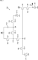
- FIG. 2 is a diagram illustrating a circuit configuration example of the pixel 100 of FIG.
- the pixel 100 includes a high-sensitivity photodiode 121-1, a low-sensitivity photodiode 121-1, a first transfer transistor 122-1, a second transfer transistor 122-2, a third transfer transistor 122-3, and a fourth transfer transistor 122-. 4, a charge storage unit 123, an FD (Floating Diffusion) unit 126, a reset transistor 127, an amplification transistor 128, and a selection transistor 129.
- FD Floating Diffusion
- a plurality of drive lines are wired to the pixels 100 as pixel drive lines 21 (FIG. 1), for example, for each pixel row.
- Various drive signals TGL, TGS, FCG, FDG, RST, and SEL are supplied through a plurality of drive lines from the vertical drive circuit 12 (FIG. 1). These drive signals are pulses in which each transistor of the pixel 100 is an NMOS transistor, so that a high level (for example, power supply VDD) state is active and a low level (for example, negative potential) is inactive. Signal.
- the high-sensitivity photodiode 121-1 is, for example, a photoelectric conversion unit including a PN junction photodiode (PD).
- the high-sensitivity photodiode 121-1 generates and accumulates charges according to the received light quantity.
- the low sensitivity photodiode 121-2 is, for example, a photoelectric conversion unit made of a PN junction photodiode (PD).
- the low-sensitivity photodiode 121-2 generates and accumulates charges corresponding to the received light quantity.
- the high-sensitivity photodiode 121-1 when comparing the high-sensitivity photodiode 121-1 and the low-sensitivity photodiode 121-2, the high-sensitivity photodiode 121-1 has a unit illuminance per unit time than the low-sensitivity photodiode 121-2. The total amount of charges (signal charges) generated per hit increases. Therefore, the high sensitivity photodiode 121-1 has higher sensitivity, and the low sensitivity photodiode 121-2 has lower sensitivity.
- the first transfer transistor 122-1 is connected between the high sensitivity photodiode 121-1 and the FD unit 126.
- a drive signal TGL is applied to the gate electrode of the first transfer transistor 122-1.
- this drive signal TGL becomes active, the transfer gate of the first transfer transistor 122-1 becomes conductive, and the charge accumulated in the high sensitivity photodiode 121-1 passes through the first transfer transistor 122-1. Transferred to the FD unit 126.
- the second transfer transistor 122-2 is connected between the FD unit 124 and the FD unit 125.
- the drive signal FCG is applied to the gate electrode of the second transfer transistor 122-2.
- the transfer gate of the second transfer transistor 122-2 becomes conductive, and the potentials of the FD portion 124 and the FD portion 125 are coupled.
- the third transfer transistor 122-3 is connected between the low sensitivity photodiode 121-2 and the FD unit 124.
- the drive signal TGS is applied to the gate electrode of the third transfer transistor 122-3.
- the transfer gate of the third transfer transistor 122-3 becomes conductive, and the charge accumulated in the low sensitivity photodiode 121-2 passes through the third transfer transistor 122-3. Then, it is transferred to a region where the potentials of the charge storage unit 123 or the FD unit 124 and the FD unit 125 are combined.
- the fourth transfer transistor 122-4 is connected between the FD unit 125 and the FD unit 126 between the second transfer transistor 122-2, the fourth transfer transistor 122-4, and the reset transistor 127.
- the drive signal FDG is applied to the gate electrode of the fourth transfer transistor 122-4.
- the transfer gate of the fourth transfer transistor 122-4 becomes conductive, and the FD portion 125 between the second transfer transistor 122-2, the reset transistor 127, and the fourth transfer transistor 122-4.
- the potential of the FD portion 126 are combined.
- the charge storage unit 123 includes a capacitor and is connected to the FD unit 124 between the second transfer transistor 122-2 and the third transfer transistor 122-3.
- the counter electrode of the charge storage unit 123 is connected between the power supply VDD that supplies the power supply VDD.
- the charge storage unit 123 stores the charge transferred or overflowed from the low sensitivity photodiode 121-2.
- the charge storage unit 123 corresponds to a pixel internal capacity (FC: Floating Capacitor) (for example, the internal capacity 123 in FIG. 10) described later.
- the FD unit 126 is FD (Floating Diffusion), and converts the charge into a voltage signal and outputs it.
- the FD unit 126 corresponds to “FD1” in a plan view (for example, a plan view of A in FIG. 6) described later.
- the FD unit 125 corresponds to “FD2” in a plan view described later, and the FD unit 124 corresponds to “FD3” in a plan view described later.
- the reset transistor 127 is connected between the power supply VDD and the FD unit 125.
- a drive signal RST and a drive signal FDG are applied to the gate electrode of the reset transistor 127.
- this drive signal RST becomes active, the reset gate of the reset transistor 127 becomes conductive, and the potential of the FD portion 126 is reset to the level of the power supply VDD.
- the amplification transistor 128 has a gate electrode connected to the FD unit 126, a drain electrode connected to the power supply VDD, and a read circuit that reads a voltage signal held in the FD unit 126, that is, an input unit of a so-called source follower circuit.
- the amplifying transistor 128 has a source electrode connected to the vertical signal line 22 (FIG. 1) via the selection transistor 129, whereby a constant current source 130 and a source follower connected to one end of the vertical signal line 22 are connected. Configure the circuit.
- the selection transistor 129 is connected between the source electrode of the amplification transistor 128 and the vertical signal line 22.
- a drive signal SEL is applied to the gate electrode of the selection transistor 129.
- the selection transistor 129 becomes conductive and the pixel 100 becomes selected.
- the pixel signal output from the amplification transistor 128 is output to the vertical signal line 22 (FIG. 1) via the selection transistor 129.
- the pixel 100 is configured as described above.
- the high-sensitivity imaging unit including the transfer transistor that transfers the charge generated at ⁇ 1 is also referred to as “high-sensitivity pixel (high-sensitivity pixel unit)”.
- the low-sensitivity photodiode 121-2 included in the pixel 100 of FIG. 2 an on-chip lens for making light incident on the low-sensitivity photodiode 121-2, and the charge generated by the low-sensitivity photodiode 121-2.
- the low-sensitivity image pickup unit including the transfer transistor that transfers the signal is also referred to as “low-sensitivity pixel (low-sensitivity pixel unit)”.
- the charge storage unit 123 is provided so that the charge overflowed by the low-sensitivity photodiode 121-2 can be stored, but a configuration in which the charge storage unit 123 is not provided is employed. You can also Therefore, in the embodiment described later, there are both a structure in which the charge storage unit 123 is provided and a structure in which the charge storage unit 123 is not provided for the low sensitivity photodiode 121-2. .
- the CMOS image sensor 10 can expand the dynamic range by using the different sensitivity between the high-sensitivity pixel having the high-sensitivity photodiode 121-1 and the low-sensitivity pixel having the low-sensitivity photodiode 121-2.
- a plurality of configurations can be adopted. Therefore, hereinafter, first to sixth embodiments corresponding to the configuration of a plurality of pixels 100 arranged two-dimensionally in the pixel array unit 11 of the CMOS image sensor 10 will be described.
- the pixel of the first embodiment is described as a pixel 900, and is distinguished from the pixels of other embodiments.
- the pixels of the second to sixth embodiments are described as a pixel 100, a pixel 200, a pixel 300, a pixel 400, and a pixel 500, respectively.
- These pixels are also referred to as the CMOS image sensor 10 ( The two-dimensional arrangement in the pixel array section 11 of FIG.
- the pixel 900 is provided as the pixel 100 arranged two-dimensionally in the pixel array unit 11 of the CMOS image sensor 10 (FIG. 1).
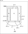
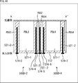
- FIG. 3 is a plan view showing the structure of the pixel 900 according to the first embodiment.
- FIG. 3 shows a plan view when one of the pixels 900 arranged two-dimensionally in the pixel array section 11 of the back-illuminated CMOS image sensor 10 (FIG. 1) is viewed from the wiring side.
- the pixel 900 illustrated in FIG. 3 has a configuration similar to that of the pixel 100 illustrated in FIG.
- the pixel 900 includes a high sensitivity photodiode 921-1 and a low sensitivity photodiode 921-2.
- the first transfer transistor 922-1 to the selection transistor 929 correspond to the first transfer transistor 122-1 to the selection transistor 129 of the pixel 100 in FIG.
- a pixel internal capacitance (FC: Floating Capacitor) 923 corresponds to the charge accumulation unit 123 of the pixel 100 in FIG.
- a MOS capacitor can be used as an example of the in-pixel capacitor 923.
- FIG. 4 a high-sensitivity photodiode (PD) 921-1 and a low-sensitivity photodiode (PD) 921-2 are formed in a semiconductor substrate 912.
- the high-sensitivity photodiode 921-1 generates and accumulates charges corresponding to the amount of light incident through the on-chip lens 911-1.
- the charge accumulated in the high sensitivity photodiode 921-1 is read out by the pixel circuit. That is, the on-chip lens 911-1, the high-sensitivity photodiode 921-1, and the pixel circuit constitute a high-sensitivity pixel 901-1.
- the low-sensitivity photodiode 921-2 generates and accumulates charges corresponding to the amount of light incident through the on-chip lens 911-2.
- the charge accumulated in the low sensitivity photodiode 921-2 is read out by the pixel circuit. That is, the low-sensitivity pixel 901-2 is configured by the on-chip lens 911-2, the low-sensitivity photodiode 921-2, and the pixel circuit.
- the silicon (Si) depth direction of the semiconductor substrate 912 of the high-sensitivity photodiode 921-1 and the low-sensitivity photodiode 921-2 is equivalent, the size in the plane direction (area of the light receiving surface) is different.
- the planar size (light receiving surface area) of the low sensitivity photodiode 921-2 is smaller than the planar size (light receiving surface area) of the high sensitivity photodiode 921-1.
- the amount of charge generated as a result of photoelectric conversion is approximately proportional to the size (thickness) in the depth direction of the photodiode.
- the amount of charge generated as a result of photoelectric conversion in the photodiode is approximately proportional to the area of the light receiving surface of the photodiode.
- the high-sensitivity photodiode 921-1 and the low-sensitivity photodiode 921-2 have the same size (thickness) in the depth direction of the photodiode. Therefore, the amount of charge (signal charge) generated per unit area of the photodiode under the unit time and unit illuminance is equal between the high sensitivity photodiode 921-1 and the low sensitivity photodiode 921-2. .
- the size of the photodiode in the planar direction is smaller in the low sensitivity photodiode 921-2 than in the high sensitivity photodiode 921-1.
- the total amount of charge (signal charge) generated in the photodiode is smaller in the low-sensitivity photodiode 921-2 than in the high-sensitivity photodiode 921-1. More specifically, it decreases in proportion to the area of the light receiving surface of the photodiode.
- the high sensitivity photodiode 921-1 and the low sensitivity photodiode 921-2 have different sensitivities, and the sensitivity of the low sensitivity photodiode 921-2 is lower than that of the high sensitivity photodiode 921-1.
- the saturation charge amount (Qs) of the photodiode is approximately proportional to the size of the photodiode in the planar direction (the area of the light receiving surface). Since both the amount of charge generated as a result of photoelectric conversion in the photodiode and the saturation charge amount (Qs) of the photodiode are approximately proportional to the area of the light receiving surface of the photodiode, the high sensitivity photodiode 921-1 and the low sensitivity If both the photodiodes 921-2 are irradiated with light having the same illuminance and the illuminance is increased, the high sensitivity photodiode 921-1 and the low sensitivity photodiode 921-2 are saturated at the same illuminance. . That is, at the same illuminance, the amount of charge generated in each photodiode has reached the saturation charge amount (Qs) of each photodiode.
- the low-sensitivity photodiode 921-2 causes the charge generated as a result of photoelectric conversion to exceed the saturation charge amount (Qs) of the low-sensitivity photodiode 921-2.
- the charge generated according to the illuminance can be overflowed and accumulated in the pixel capacitor 923 and output as a signal charge.
- the high sensitivity photodiode 921-1 generates a high sensitivity photodiode.
- Overflow to the P-well layer which is a P-type impurity region around 921-1. As described above, the charge overflowed to the P well layer is absorbed by the drain region of the NMOS transistor included in the pixel 900 having the same structure as the pixel 100 shown in FIG. 2, and is not used as the signal charge.
- a low-sensitivity pixel portion (low-sensitivity pixel 901-2) including a pixel internal capacitance 923 and a low-sensitivity photodiode 921-2, and a high-sensitivity pixel portion (high-sensitivity pixel) including a high-sensitivity photodiode 921-1.
- 901-1) represents input / output characteristics.
- the horizontal axis represents the illuminance of light applied to each photodiode, and the vertical axis represents the amount of charge output from each photodiode.
- the dotted line in the figure represents the input / output characteristics of the high-sensitivity pixel portion (high-sensitivity pixel 901-1), and the alternate long and short dash line in the figure represents the input-output characteristics of the low-sensitivity pixel portion (low-sensitivity pixel 901-2). Represents.
- the low-sensitivity pixel unit In the high-sensitivity pixel portion, at a lower illuminance than the low-sensitivity pixel portion, the charge generated as a result of photoelectric conversion reaches the saturation charge amount (Qs), and the output is saturated.
- the low-sensitivity pixel unit outputs a signal charge corresponding to the illuminance even in the illuminance where the output of the high-sensitivity pixel unit is saturated. That is, in the input / output characteristics shown in FIG. 5, the low sensitivity pixel unit has a wider input range (illuminance range in which an output corresponding to the illuminance can be obtained) than the high sensitivity pixel unit, and the output range ( The range of the output charge amount) is widened. In other words, it can be said that the low sensitivity pixel unit has a wider dynamic range than the high sensitivity pixel unit.
- the CMOS image sensor 10 including the pixel 900 includes an amplifier that multiplies the output of the low-sensitivity pixel unit.
- the column signal processing circuit 13 shown in FIG. 1 includes this amplifier. The operation of this amplifier will be described below with reference to FIG.
- the high-sensitivity pixel portion has higher sensitivity than the low-sensitivity pixel in the illuminance region where the output is not saturated. For this reason, in FIG. 5 (inside the dotted line of “sensitivity ratio”), in the illuminance region where the output (dotted line) of the high-sensitivity pixel unit is not saturated, the inclination is the output of the low-sensitivity pixel unit (dashed line) It is larger than the slope. In other words, in this illuminance region, the output of the high-sensitivity pixel unit is larger than the output of the low-sensitivity pixel unit, and of course, the S / N ratio (SignalSignNoise ratio, hereinafter referred to as S / N) is also large. Get higher.
- FIG. 5 (outside the dotted line of “sensitivity ratio”), in the region where the output of the high-sensitivity pixel portion is saturated, an output corresponding to the illuminance is obtained from the low-sensitivity pixel portion. It becomes smaller than the slope of the output before the pixel portion is saturated. Therefore, in the CMOS image sensor 10 (FIG. 1) including the pixels 900, the amplifier (for example, the amplifier included in the column signal processing circuit 13 in FIG. 1) described above is used for the output obtained from the low sensitivity pixel unit. Try to multiply the gain.
- the amplifier for example, the amplifier included in the column signal processing circuit 13 in FIG.
- the slope of the output of the high-sensitivity pixel unit before saturation is the same as the slope of the output after gain increase, which is obtained by multiplying the output of the low-sensitivity pixel unit before saturation by a gain.
- a gain is applied to the output of the low-sensitivity pixel unit.
- the solid line in FIG. 5 represents the output of the low-sensitivity pixel unit after this gain increase (arrows A1 and A2 in the figure).
- the input irradiates the photodiode from the illuminance range where the high sensitivity pixel unit outputs the electric charge according to the illuminance to the illuminance range where the low sensitivity pixel unit outputs the electric charge according to the illuminance.
- a linear output (amount of charge output from the photodiode) can be obtained with respect to (illuminance of light).
- the output before saturation of the high-sensitivity pixel portion indicated by the dotted line in FIG. 5 has an S / N ratio higher than the output before saturation of the low-sensitivity pixel portion indicated by the one-dot chain line in FIG. Get higher.
- the output of the low sensitivity pixel unit has a lower S / N ratio than the output of the high sensitivity pixel unit.
- the CMOS image sensor 10 (FIG. 1) including the pixels 900 has data based on the output of the high-sensitivity pixel unit in the illuminance range in which the high-sensitivity pixel unit in FIG. 5 outputs charges according to the illuminance.
- data based on the output of the low-sensitivity pixel unit after gain increase can be output as pixel data of the imaging result.
- the CMOS image sensor 10 (FIG. 1) including the pixels 900 has a wider dynamic range in the direction of higher illuminance than that of the prior art, and can obtain characteristics with good S / N in the low illuminance region. it can.
- the CMOS image sensor 10 (FIG. 1) including the pixel 900 has a low-sensitivity pixel that does not apply gain without providing an amplifier that applies gain to the low-sensitivity pixel unit.
- Data based on the output of the unit may be output as pixel data of the imaging result. In this case, it is desirable to multiply the data based on the output of the low sensitivity pixel unit by a gain on the device side that receives the output of the CMOS image sensor 10.
- Second Embodiment Structure in which the size in the depth direction of a low-sensitivity PD is limited>
- the size in the planar direction of the low-sensitivity photodiode of the low-sensitivity pixel is formed to be smaller than the size in the planar direction of the high-sensitivity photodiode of the high-sensitivity pixel.
- the size of the low-sensitivity photodiode in the low-sensitivity pixel is limited in the depth direction to reduce the amount of charge generated as a result of photoelectric conversion.
- the size in the planar direction of the low-sensitivity photodiode of the low-sensitivity pixel can be made equal to or larger than the size in the planar direction of the high-sensitivity photodiode.
- the pixels 100A to 100D are described as the pixels 100 arranged two-dimensionally in the pixel array unit 11 of the CMOS image sensor 10 (FIG. 1).
- the pixels 100A and 100B are described.
- the pixel 100C and the pixel 100D have a structure having the pixel capacity 123, while the structure does not have the pixel capacity 123. Therefore, the pixel circuits of the pixel 100C and the pixel 100D correspond to the configuration of the pixel circuit shown in FIG. 2, but the pixel circuits of the pixel 100A and the pixel 100B are the pixel internal capacitance 123 in the pixel circuit shown in FIG. This corresponds to a configuration in which no is provided.
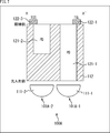
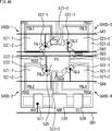
- the pixel 100A having a structure in which the size of the low-sensitivity photodiode (PD) in the depth direction is limited will be described with reference to the plan view of FIG. 6 and the cross-sectional view of FIG.
- FIG. 6 is a plan view showing the structure of the pixel 100A.
- a in FIG. 6 represents a plan view when one of the pixels 100A arranged two-dimensionally in the pixel array unit 11 of the CMOS image sensor 10 (FIG. 1) is viewed from the wiring side.
- B of FIG. 6 represents a plan view when the pixel 100A is viewed from the light incident side.
- FIG. 7 a high sensitivity photodiode (PD) 121-1 and a low sensitivity photodiode (PD) 121-2 are formed in silicon (Si) of a semiconductor substrate 112.
- the first transfer transistor 122-1 and the third transfer transistor 122-3 which will be described later, are also shown for convenience.
- the high-sensitivity photodiode 121-1 generates and accumulates electric charges according to the amount of light incident through the on-chip lens 111-1. Then, the charge accumulated in the high-sensitivity photodiode 121-1 is read out by the first transfer transistor 122-1 operating in accordance with the drive signal TGL applied to the gate electrode.
- a high-sensitivity pixel 101A-1 is configured by a pixel circuit such as the above.
- the low-sensitivity photodiode 121-2 generates and accumulates charges corresponding to the amount of light incident through the on-chip lens 111-2.
- the charge accumulated in the low-sensitivity photodiode 121-2 is read out by the third transfer transistor 122-3 operating according to the drive signal TGS applied to the gate electrode.
- a low-sensitivity pixel 101A-2 is configured by a pixel circuit such as the above.
- the size (area of the light receiving surface) in the planar direction of the high-sensitivity photodiode 121-1 and the low-sensitivity photodiode 121-2 is: Although the sizes are the same (substantially the same), the size of the semiconductor substrate 112 in the depth direction of silicon (Si) is different. Specifically, the size of the low sensitivity photodiode 121-2 in the depth direction is smaller than the size of the high sensitivity photodiode 121-1 in the depth direction.
- the size of the low sensitivity photodiode 121-2 is limited, and the high sensitivity photodiode 121 is limited.
- the size in the depth direction is made smaller than -1. Further, in this case, as shown in the plan view of the wiring side of FIG. 6A and the light incident side of FIG. 6B, the high-sensitivity photodiode 121-1 and the low-sensitivity photodiode 121-2 in the planar direction.
- the size (area of the light receiving surface) is the same (substantially the same) size.
- the pixel 100A of the second embodiment shown in FIGS. 6 and 7 is compared with the pixel 900 of the first embodiment shown in FIGS.
- the pixel 900 shown in FIG. 3 and FIG. 4 has a planar size (light receiving surface area) of the low sensitivity photodiode 921-2 and a planar size (light receiving surface area) of the high sensitivity photodiode 921-1.
- the amount of charge generated as a result of photoelectric conversion in the low-sensitivity photodiode 921-2 is made smaller than the amount of charge generated as a result of photoelectric conversion in the high-sensitivity photodiode 921-1.
- the low-sensitivity photodiode 921-2 includes an in-pixel capacitor 923 as charge storage means other than the low-sensitivity photodiode 921-2 in order to accumulate more charge generated as a result of photoelectric conversion.
- the low-sensitivity pixel of the pixel 900 including the low-sensitivity photodiode 921-2 and the pixel capacitance 923 can be stored.
- the unit (low-sensitivity pixel 901-2) accumulates electric charges according to the illuminance and outputs it without saturating the output over a wide illuminance range.
- the pixel 900 according to the first embodiment shown in FIGS. 3 and 4 can obtain characteristics with a wider dynamic range than the conventional technique.
- the size (thickness) of the low sensitivity photodiode 121-2 in the depth direction is the same as the size (thickness) of the high sensitivity photodiode 121-1.
- the amount of charge generated as a result of photoelectric conversion in the low-sensitivity photodiode 121-2 is made smaller than the amount of charge generated as a result of photoelectric conversion in the high-sensitivity photodiode 121-1.
- the size of the low-sensitivity photodiode 121-2 in the plane direction (the area of the light receiving surface) is set in the pixel 900.
- the saturation charge amount (Qs) of the low-sensitivity photodiode 121-2 is increased by making it larger than the size (area of the light-receiving surface) of the low-sensitivity photodiode 921-2 provided.
- the low-sensitivity pixel portion (low-sensitivity pixel) of the pixel 100A including the low-sensitivity photodiode 121-2. 101A-2) can accumulate and output charges according to the illuminance without saturating the output over a wide illuminance range.
- the pixel 100A of the second embodiment shown in FIGS. 6 and 7 can obtain characteristics with a wider dynamic range than the prior art.
- the pixel 100A accumulates the charge generated in the low sensitivity photodiode 121-2 in the photodiode.
- the photodiode stores charge in a potential well generated in the depleted photodiode, while the MOS capacitor has free electrons. Charges are accumulated using a large number of metals or degenerate semiconductors as electrodes. For this reason, it is less noise to store charges in a photodiode than to store charges in a MOS capacitor.
- the pixel 100A has the structure shown in FIGS. 6 and 7, so that a higher S / N can be obtained at the output of the low-sensitivity photodiode than the pixel 900 shown in FIGS. it can.
- the CMOS image sensor 10 (FIG. 1) including the pixel 100A has a wider dynamic range in the direction of higher illuminance than that of the prior art, and has a good S / N in both low illuminance and high illuminance regions. Can be obtained.
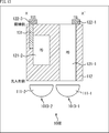
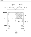
- the pixel 100B having a structure in which the position of the low sensitivity photodiode (PD) in the depth direction is changed will be described with reference to the plan view of FIG. 8 and the cross-sectional view of FIG.
- FIG. 8 is a plan view showing the structure of the pixel 100B.
- a in FIG. 8 represents a plan view when one of the pixels 100B arranged two-dimensionally in the pixel array unit 11 of the CMOS image sensor 10 (FIG. 1) is viewed from the wiring side.
- B in FIG. 8 represents a plan view when the pixel 100B is viewed from the light incident side.
- FIG. 9 a high sensitivity photodiode (PD) 121-1 and a low sensitivity photodiode (PD) 121-2 are formed in silicon (Si) of a semiconductor substrate 112.
- the size of the high sensitivity photodiode 121-1 and the low sensitivity photodiode 121-2 in the planar direction is equal (substantially the same) or larger.
- the size of the low sensitivity photodiode 121-2 in the depth direction is smaller than the size of the high sensitivity photodiode 121-1 in the depth direction.
- the vertical transistor 131 is formed on the silicon (Si) of the semiconductor substrate 112, and the charge accumulated in the low-sensitivity photodiode 121-2 is transferred to the third transfer transistor 122- through the vertical transistor 131. 3 is read.
- the size of the low sensitivity photodiode 121-2 is limited, and the high sensitivity photodiode is limited.
- the size in the depth direction is smaller than that of 121-1.
- the sensitivity of the low-sensitivity pixel 101B-2 can be adjusted by changing the position of the low-sensitivity photodiode 121-2 in the depth direction.
- the sensitivity of the low-sensitivity pixel 101B-2 improves as the position in the depth direction of the low-sensitivity photodiode 121-2 moves toward the light incident side, while the sensitivity of the low-sensitivity pixel 101B-2 increases toward the wiring side.
- the sensitivity difference between the high-sensitivity pixel 101B-1 and the low-sensitivity pixel 101B-2 is optimized by setting the position of the low-sensitivity photodiode 121-2 in the depth direction to an appropriate position. be able to.
- the planar direction of the high sensitivity photodiode 121-1 and the low sensitivity photodiode 121-2. are equal (substantially the same size).
- the low sensitivity photodiode 121-2 in the depth direction has been described, but the size (width) of the low-sensitivity photodiode 121-2 in the planar direction is changed. Also good.
- the low sensitivity photodiode can be obtained by forming the vertical transistor 131 according to the structure. The charge accumulated in 121-2 can be read out.
- the pixel 100B has the cross-sectional structure shown in FIG. 8 and FIG. 9, so that the low-sensitivity pixel 101B-2 reduces the amount of charge generated as a result of photoelectric conversion and generates the generated charge. The amount that can be stored is increased. Thereby, the pixel 100B can obtain characteristics with a wide dynamic range.
- both the high-sensitivity pixel 101B-1 and the low-sensitivity pixel 101B-2 accumulate the generated charges in the photodiode, so that the S / N is good in both the low and high illuminance regions. Characteristics can be obtained.
- the sensitivity of the low-sensitivity pixel 101B-2 can be adjusted by changing the position in the depth direction of the low-sensitivity photodiode 121-2 and the size (width) in the planar direction.
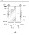
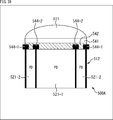
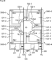
- the pixel 100C having a structure in which the low-sensitivity pixel has a pixel internal capacitance (FC) will be described.
- FIG. 10 is a plan view showing the structure of the pixel 100C.
- a in FIG. 10 represents a plan view when one of the pixels 100C arranged two-dimensionally in the pixel array unit 11 of the CMOS image sensor 10 (FIG. 1) is viewed from the wiring side.
- B in FIG. 10 represents a plan view when the pixel 100C is viewed from the light incident side.
- FIG. 11 a high-sensitivity photodiode (PD) 121-1 and a low-sensitivity photodiode (PD) 121-2 are formed in silicon (Si) of a semiconductor substrate 112.
- the size (area of the light receiving surface) in the planar direction of the high sensitivity photodiode 121-1 and the low sensitivity photodiode 121-2 is the same (approximately).
- the size in the depth direction of the low-sensitivity photodiode 121-2 is smaller than the size in the depth direction of the high-sensitivity photodiode 121-1.
- the low-sensitivity pixel 101C-2 has a pixel internal capacitance (FC) 123 as shown in the plan view on the wiring side of FIG. This is different from the structure of the low-sensitivity pixel 101A-2 of the pixel 100A shown in the plan view on the wiring side. That is, in the low-sensitivity pixel 101C-2, the charges overflowing from the low-sensitivity photodiode 121-2 are accumulated by the pixel capacitance 123.
- FC pixel internal capacitance
- the saturation charge amount (Qs) of the low sensitivity pixel 101C-2 overflows to the in-pixel capacitance 123. It will be expanded according to the amount of charge.
- the size of the low-sensitivity photodiode 121-2 in the planar direction can be equal to or larger than the size of the high-sensitivity photodiode 121-1 in the planar direction. Saturation charge (Qs) can be gained to some extent, so it is superior in S / N characteristics at low illumination.
- the pixel 100C has the cross-sectional structure shown in FIGS. 10 and 11, and thus contributes to the saturation charge amount (Qs) of the low-sensitivity pixel 101C-2. Since a certain amount of saturation charge (Qs) can be obtained without reducing the size in the plane direction, it is difficult for the charge to overflow into the pixel internal capacity 123, which is superior in S / N characteristics at low illumination. .
- the saturation charge amount (Qs) of the low sensitivity pixel 101C-2 is the charge overflowed to the in-pixel capacitance 123. It will be expanded according to the amount.
- the low-sensitivity pixel has a pixel internal capacitance (FC), and the position of the low-sensitivity photodiode (PD) in the depth direction is changed.
- FC pixel internal capacitance
- PD low-sensitivity photodiode
- FIG. 12 is a plan view showing the structure of the pixel 100D.
- a in FIG. 12 represents a plan view when one of the pixels 100D arranged two-dimensionally in the pixel array unit 11 of the CMOS image sensor 10 (FIG. 1) is viewed from the wiring side.
- B of FIG. 12 represents a plan view when the pixel 100D is viewed from the light incident side.
- FIG. 13 a high sensitivity photodiode (PD) 121-1 and a low sensitivity photodiode (PD) 121-2 are formed in silicon (Si) of a semiconductor substrate 112.
- the size (area of the light receiving surface) in the planar direction of the high sensitivity photodiode 121-1 and the low sensitivity photodiode 121-2 is the same (substantially).
- the size in the depth direction of the low-sensitivity photodiode 121-2 is smaller than the size in the depth direction of the high-sensitivity photodiode 121-1.
- the position of the low sensitivity photodiode 121-2 in the depth direction is changed from the position on the wiring side to the position closer to the light incident side.
- the sensitivity of the low sensitivity pixel 101D-2 is adjusted.
- the charge accumulated in the low-sensitivity photodiode 121-2 is read out by the third transfer transistor 122-3 via the vertical transistor 131.
- the low-sensitivity pixel 101D-2 has a pixel internal capacitance (FC) 123. This is different from the structure of the low-sensitivity pixel 101B-2 of the pixel 100B shown in the plan view on the wiring side. That is, in the low-sensitivity pixel 101D-2, the charges overflowing from the low-sensitivity photodiode 121-2 are accumulated by the pixel capacitance 123.
- FC pixel internal capacitance
- the saturation charge amount (Qs) of the low sensitivity pixel 101D-2 overflows to the in-pixel capacitance 123. It will be expanded according to the amount of charge.
- the low-sensitivity photodiode 121-2 of the low-sensitivity pixel 101D-2 is formed at a position away from the ion-implanted wiring side, so that it is difficult to form a steep PN junction.
- the saturation charge amount (Qs) of only the low sensitivity photodiode 121-2 becomes small.
- the charge from the low-sensitivity photodiode 121-2 overflows and accumulates in the pixel capacitance 123, so there is no problem with the saturation charge amount (Qs) as the low-sensitivity pixel 101D-2.
- the pixel 100D has the cross-sectional structure shown in FIGS. 12 and 13, and thus contributes to the saturation charge amount (Qs) of the low-sensitivity pixel 101D-2.
- a certain amount of saturation charge (Qs) can be earned without reducing the size in the planar direction.
- the saturation charge amount (Qs) of the low sensitivity pixel 101D-2 is the charge overflowed to the in-pixel capacitance 123. It will be expanded according to the amount.
- the sensitivity of the low-sensitivity pixel 101D-2 can be adjusted by changing the position in the depth direction and the size (width) in the planar direction of the low-sensitivity photodiode 121-2.
- the pixels 100A to 100D have been described as the second embodiment.
- the sensitivity is lowered, and the size of the low-sensitivity pixel in the planar direction of the low-sensitivity photodiode is reduced. Is equal to or larger than the size of the high-sensitivity photodiode in the planar direction.
- the amount of generated charges can be accumulated while reducing the amount of charges generated as a result of photoelectric conversion.
- the pixels 100A to 100D can obtain characteristics with a wide dynamic range.
- a certain amount of saturation charge (Qs) can be obtained, so that it is difficult for the charge to overflow into the pixel internal capacity, and the S / N has a characteristic advantage.
- the “depth direction” of silicon (Si) of the semiconductor substrate 112 described above is an “optical axis direction” in which light enters.
- the “plane direction” is a “direction perpendicular to the optical axis”.
- FC Floating Capacitor
- LFIC Lateral Over Flow Integration Capacitor
- the photodiode is formed by implanting ions from the wiring side. This makes it easier to form a high-capacity photodiode using a PN junction. That is, in order to increase the saturation charge amount (Qs) of the low-sensitivity pixel, the size in the plane direction on the wiring side of the low-sensitivity photodiode may be increased. The higher the saturation charge amount (Qs) of the low-sensitivity photodiode of the low-sensitivity pixel, the higher the dynamic range can be obtained.
- the size of the low-sensitivity pixel in the plane direction on the wiring side of the low-sensitivity photodiode is made larger than the size in the plane direction on the light incident side so that the saturation charge amount ( Qs) can be expanded.
- the saturation charge amount (Qs) of the low-sensitivity pixel is increased, and a high dynamic range can be obtained.
- the pixels 200A to 200F are described as the pixels 200 arranged two-dimensionally in the pixel array unit 11 of the CMOS image sensor 10 (FIG. 1). However, the pixels 200A and 200F are described.
- the pixel 200B to the pixel 200E have a structure having the pixel capacitor 223, while the pixel 200B to the pixel 200E have a structure without the pixel capacitor 223.
- pixel circuits such as the high-sensitivity photodiode 221-1, the low-sensitivity photodiode 221-2, and the first transfer transistor 222-1 to the selection transistor 229 have high sensitivity in the pixel 100 in FIG. This corresponds to pixel circuits such as the photodiode 121-1, the low-sensitivity photodiode 121-2, and the first transfer transistor 122-1 to the selection transistor 129.
- the pixel circuits of the pixel 200B and the pixel 200E correspond to the configuration of the pixel circuit shown in FIG. 2, but the pixel circuits of the pixel 200A and the pixel 200F have a pixel internal capacitance 223 in the pixel circuit shown in FIG. This corresponds to a configuration in which no is provided.
- (2-A) Basic structure Structure in which the incident light side and the wiring side of the low sensitivity PD have different sizes in the plane direction
- a pixel 200A having a structure in which the size of the incident light side and the wiring side of the low sensitivity photodiode (PD) are different from each other will be described.
- FIG. 14 is a plan view showing the structure of the pixel 200A.
- a in FIG. 14 represents a plan view when one of the pixels 200A arranged two-dimensionally in the pixel array section 11 of the CMOS image sensor 10 (FIG. 1) is viewed from the wiring side.
- B of FIG. 14 represents a plan view when the pixel 200A is viewed from the light incident side.
- FIG. 15 a high sensitivity photodiode (PD) 221-1 and a low sensitivity photodiode (PD) 221-2 are formed in silicon (Si) of a semiconductor substrate 212.
- the high-sensitivity photodiode 221-1 generates and accumulates charges corresponding to the amount of light incident through the on-chip lens 211-1.
- the charge accumulated by the high sensitivity photodiode 221-1 is read out by a pixel circuit such as the first transfer transistor 222-1.
- a high-sensitivity pixel 201A-1 is configured by a pixel circuit such as the above.
- the low-sensitivity photodiode 221-2 generates and accumulates charges corresponding to the amount of light incident through the on-chip lens 211-2. Then, the charge accumulated by the high sensitivity photodiode 221-2 is read out by the pixel circuit such as the third transfer transistor 222-3 via the vertical transistor 231.
- a low-sensitivity pixel 201A-2 is configured by a pixel circuit such as the above.
- the size of the low-sensitivity photodiode 221-2 in the depth direction is the size of the high-sensitivity photodiode 221-1 in the depth direction. It becomes a smaller size.
- the size of the low-sensitivity photodiode 221-2 in the planar direction is different from the size in the planar direction on the light incident side and the size in the planar direction on the wiring side. Specifically, in the low sensitivity photodiode 221-2, the size in the plane direction on the wiring side is larger than the size in the plane direction on the light incident side.
- the difference in sensitivity between the high-sensitivity pixel 201A-1 and the low-sensitivity pixel 201A-2 is set by the size of the photodiode in the depth direction, and thus the planar direction of the low-sensitivity photodiode 221-2. Is not required to be smaller than the size of the high-sensitivity photodiode 221-1 in the planar direction, and can be equal to or larger than the size of the high-sensitivity photodiode 221-1.
- the size of the light incident side plane direction contributing to the sensitivity of the low sensitivity photodiode 221-2 of the low sensitivity pixel 201A-2 is set to the plane on the wiring side contributing to the saturation charge amount (Qs).
- the high sensitivity photodiode 221-1 of the high sensitivity pixel 201A-1 and the low sensitivity photodiode 221-2 of the low sensitivity pixel 201A-2 are formed on the semiconductor substrate 212, ions are implanted from the wiring side. As a result, a photodiode is formed. On the wiring side, it becomes easier to form a high-capacity photodiode by a PN junction.
- the size of the low-sensitivity photodiode 221-2 on the wiring side may be increased, and the low-sensitivity photodiode 221-2. Then, the size in the plane direction on the wiring side is set to be larger than the size in the plane direction on the light incident side. Thereby, the saturation charge amount (Qs) of the low-sensitivity pixel 201A-2 is increased, and a high dynamic range can be obtained.
- the pixel 200A has the structure shown in FIGS. 14 and 15, and thereby contributes to the saturation charge amount (Qs) of the low-sensitivity pixel 101A-2.
- the saturation charge amount (Qs) of the low-sensitivity pixel 201A-2 can be increased by widening the size in the planar direction of the light incident side.
- the plane size on the light incident side of the low sensitivity photodiode 221-2 that contributes to the sensitivity of the low sensitivity pixel 201A-2 is smaller than the size in the plane direction on the wiring side. While the saturation charge amount (Qs) of the high-sensitivity pixel 201A-1 and the low-sensitivity pixel 201A-2 is ensured to be equal to or higher, the sensitivity of the low-sensitivity pixel 201A-2 can be further reduced. The effect of expanding the dynamic range in the pixel 200A is increased.
- a pixel 200B having a structure in which a low-sensitivity pixel has a pixel internal capacitance (FC) will be described with reference to a plan view of FIG. 16 and a cross-sectional view of FIG.
- FIG. 16 is a plan view showing the structure of the pixel 200B.
- a in FIG. 16 represents a plan view when one of the pixels 200B arranged two-dimensionally in the pixel array unit 11 of the CMOS image sensor 10 (FIG. 1) is viewed from the wiring side.
- B of FIG. 16 represents a plan view when the pixel 200B is viewed from the light incident side.
- FIG. 17 a high sensitivity photodiode (PD) 221-1 and a low sensitivity photodiode (PD) 221-2 are formed in silicon (Si) of the semiconductor substrate 112.
- the size of the low sensitivity photodiode 221-2 in the depth direction is larger than the size of the high sensitivity photodiode 221-1 in the depth direction. Small size.
- the size in the plane direction on the wiring side is larger than the size in the plane direction on the light incident side.
- the low sensitivity pixel 201B-2 has a pixel internal capacity (FC) 223. This is different from the structure of the low-sensitivity pixel 201A-2 of the pixel 200A shown in the plan view of FIG. That is, in the low-sensitivity pixel 201B-2 of the pixel 200B, the charges overflowing from the low-sensitivity photodiode 221-2 are accumulated by the pixel capacitance 223.
- FC pixel internal capacity
- the pixel 200B has the structure shown in FIGS. 16 and 17, and thereby contributes to the saturation charge amount (Qs) of the low-sensitivity pixel 101B-2, which is on the wiring side of the low-sensitivity photodiode 221-2.
- the saturation charge amount (Qs) of the low-sensitivity pixel 201B-2 can be increased by expanding the size in the planar direction of the light-receiving side.
- the plane size on the light incident side of the low sensitivity photodiode 221-2 that contributes to the sensitivity of the low sensitivity pixel 201B-2 is smaller than the size in the plane direction on the wiring side. While the saturation charge amount (Qs) of the high-sensitivity pixel 201B-1 and the low-sensitivity pixel 201B-2 is ensured to be equal to or higher, the sensitivity of the low-sensitivity pixel 201B-2 can be further reduced. The effect of expanding the dynamic range in the pixel 200B is increased.
- the saturation charge amount (Qs) of the low-sensitivity pixel 201B-2 is the charge overflowed to the in-pixel capacitance 223. It will be expanded according to the amount.
- a pixel 200C having a structure in which a low-sensitivity photodiode (PD) is formed around the high-sensitivity photodiode (PD) will be described with reference to a plan view of FIG. 18 and a cross-sectional view of FIG.
- FIG. 18 is a plan view showing the structure of the pixel 200C.
- a in FIG. 18 represents a plan view when one of the pixels 200 ⁇ / b> C arranged two-dimensionally in the pixel array unit 11 of the CMOS image sensor 10 (FIG. 1) is viewed from the wiring side.
- B of FIG. 18 represents a plan view when the pixel 200C is viewed from the light incident side.
- FIG. 19 a high-sensitivity photodiode (PD) 221-1 and a low-sensitivity photodiode (PD) 221-2 are formed in the silicon (Si) of the semiconductor substrate 212.
- Reference numeral 221-2 is formed around (around) the high-sensitivity photodiode 221-1 (a plan view on the light incident side in FIG. 18).
- the low-sensitivity photodiode 221-2 of the low-sensitivity pixel 201C-2 is formed in a region outside the condensing point of the on-chip lens 211, so that the high-sensitivity pixel 201C-1 And a low sensitivity pixel 201C-2.
- the size of the high-sensitivity photodiode 221-1 in the planar direction is different between the light incident side and the wiring side. Specifically, in the high sensitivity photodiode 221-1, the size in the planar direction on the wiring side is smaller than the size in the planar direction on the light incident side.
- the size of the low-sensitivity photodiode 221-2 in the planar direction is different between the light incident side and the wiring side. Specifically, in the low-sensitivity photodiode 221-2, the size in the plane direction on the wiring side is larger than the size in the plane direction on the light incident side.
- the saturation charge amount (Qs) of the low-sensitivity photodiode 221-2 of the low-sensitivity pixel 201C-2 is larger, a higher dynamic range can be expected. Therefore, also in the pixel 200C, the above-described pixel 200A (FIG. 15). Similarly to the pixel 200B (FIG. 17), the size of the low sensitivity photodiode 121-2 in the plane direction on the wiring side is made larger than the size in the plane direction on the light incident side.
- the size in the planar direction on the wiring side of the high-sensitivity photodiode 221-1 is set in order to secure a region for increasing the size in the planar direction on the wiring side of the low-sensitivity photodiode 121-2. It is small.
- the pixel 200C has a structure in which the low sensitivity pixel 201C-2 is arranged around (periphery) the high sensitivity pixel 201C-1, so that the low sensitivity photodiode 221 of the low sensitivity pixel 201C-2 is provided. -2 is formed in a region deviated from the condensing point of the on-chip lens 211, and thus the sensitivity can be reduced.
- the saturation charge amount (Qs) is ensured by setting the size in the plane direction on the wiring side to be larger than the size in the plane direction on the light incident side in the low-sensitivity photodiode 221-2.
- the sensitivity can be lowered.
- a part of the low-sensitivity photodiode 221-2 has a high-sensitivity photodiode. Although it is smaller than the diode 221-1, the entire low sensitivity photodiode 221-2 may be smaller than the high sensitivity photodiode 221-1.
- the pixel 200C has the structure shown in FIGS. 18 and 19, and thereby contributes to the saturation charge amount (Qs) of the low-sensitivity pixel 101C-2.
- the saturation charge amount (Qs) of the low-sensitivity pixel 201C-2 can be increased by widening the size in the planar direction of the pixel.
- the plane size on the light incident side of the low sensitivity photodiode 221-2 that contributes to the sensitivity of the low sensitivity pixel 201C-2 is smaller than the size in the plane direction on the wiring side.
- the saturation charge amount (Qs) of the high-sensitivity pixel 201C-1 and the low-sensitivity pixel 201C-2 can be equalized or higher, and the sensitivity of the low-sensitivity pixel 201C-2 can be further reduced. The effect of expanding the dynamic range in the pixel 200C is increased.
- a pixel 200D having a structure in which the wiring side of a high-sensitivity photodiode (PD) is formed by a PN junction will be described with reference to the plan view of FIG. 20 and the cross-sectional views of FIGS.
- FIG. 20 is a plan view showing the structure of the pixel 200D.
- a in FIG. 20 represents a plan view when one of the pixels 200D arranged two-dimensionally in the pixel array section 11 of the CMOS image sensor 10 (FIG. 1) is viewed from the wiring side.
- B of FIG. 20 represents a plan view when the pixel 200D is viewed from the light incident side.
- the structure shown in the cross sectional view of FIG. 21 is obtained.
- the pixel 200D of FIG. 21 as in the pixel 200C (FIG. 19) described above, the low sensitivity photodiode 221-2 is formed around (around) the high sensitivity photodiode 221-1 (B in FIG. 20). Plan view of the light incident side of FIG.
- the low-sensitivity photodiode 221-2 of the low-sensitivity pixel 201D-2 is formed in a region outside the condensing point of the on-chip lens 211, so that the high-sensitivity pixel 201D- 1 and a low sensitivity pixel 201D-2.
- the pixel 200D has a size in the plane direction on the wiring side smaller than the size in the plane direction on the light incident side in the high-sensitivity photodiode 221-1.
- the size in the plane direction on the wiring side is larger than the size in the plane direction on the light incident side.
- an N + layer 213 that is an N-type region and a P + layer 214 that is a P-type region are formed on the wiring side of the high-sensitivity photodiode 221-1, and a PN junction is formed.
- ions are implanted into the semiconductor substrate 212 from the wiring side. It is easy to form a high-capacity photodiode. That is, in order to increase the saturation charge amount (Qs), the size in the planar direction on the wiring side of the photodiode may be increased.
- the wiring of the low-sensitivity photodiode 121-2 The size in the plane direction on the side is increased.
- the size in the planar direction on the wiring side of the high-sensitivity photodiode 221-1 is reduced.
- both the high-sensitivity photodiode 221-1 of the high-sensitivity pixel 201D-1 and the low-sensitivity photodiode 221-2 of the low-sensitivity pixel 201D-2 are connected to the plane direction on the light incident side and the wiring side.
- the size is different in the plane direction.
- a PN junction that contributes to the saturation charge amount (Qs) is formed on the wiring side, so that the high-capacity high-sensitivity photodiode 221- 1 is formed. 1 is formed.
- a PN junction may also be formed at a portion in the middle of reducing the size of the high-sensitivity photodiode 221-1 in the planar direction.
- a PN junction is formed in the pixel 200E.
- the pixel 200D has the structure shown in FIGS. 20 and 21, and the pixel 200E has the structure shown in FIGS. 20 and 22. Therefore, the low-sensitivity pixel 201D-2 (201E-2 ) That contributes to the saturation charge amount (Qs) of the low-sensitivity photodiode 221-2, the size in the plane direction on the wiring side of the low-sensitivity photodiode 221-2 is made wider than the size in the plane direction on the light incident side, thereby reducing the low-sensitivity pixel 201D-2 (201E Since the saturation charge amount (Qs) of -2) can be increased, a high dynamic range can be obtained.
- the saturation charge amount (Qs) of -2 Since the saturation charge amount (Qs) of -2) can be increased, a high dynamic range can be obtained.
- the plane size on the light incident side of the low sensitivity photodiode 221-2 that contributes to the sensitivity of the low sensitivity pixel 201D-2 (201E-2) is smaller than the size in the plane direction on the wiring side. Therefore, the saturation charge amount (Qs) of the high-sensitivity pixel 201D-1 (201E-1) and the low-sensitivity pixel 201D-2 (201E-2) is ensured to be equal to or higher than the low-sensitivity pixel 201D-2.
- the sensitivity of (201E-2) can be further reduced, and the effect of expanding the dynamic range in the pixel 200D is increased.
- the pixel 200F will be described with reference to the cross-sectional view of FIG.
- the size in the depth direction of the low sensitivity photodiode 221-2 is larger than the size in the depth direction of the high sensitivity photodiode 221-1 in the same manner as the pixel 200A (FIG. 15) described above. Small size.
- the size in the plane direction on the wiring side is larger than the size in the plane direction on the light incident side.
- the external size of the on-chip lens 211-2 that condenses the light on the low-sensitivity photodiode 221-2 is in the plane direction on the light incident side of the low-sensitivity photodiode 221-2. It is matched to the size.
- the on-chip lens 211-1 of the high-sensitivity pixel 201A-1 and the on-chip lens 211-2 of the low-sensitivity pixel 201A-2 have the same outer size.
- the on-chip lens 211-1 of the high-sensitivity pixel 201F-1 and the on-chip lens 211-2 of the low-sensitivity pixel 201F-2 are different from each other in the pixel 200F in FIG.
- the external size of the on-chip lens 211-2 can be changed according to the size of the low-sensitivity photodiode 221-2 in the planar direction on the light incident side.
- the pixels 200A to 200F have been described as the third embodiment.
- the size of the low-sensitivity pixel in the planar direction on the wiring side of the low-sensitivity photodiode is made larger than the size in the planar direction on the light incident side, and the saturation charge amount ( Qs) can be extended.
- the saturation charge amount (Qs) of the high-sensitivity pixel and the low-sensitivity pixel can be equalized or higher, and the sensitivity of the low-sensitivity pixel can be further reduced. This is advantageous for expanding the dynamic range of pixels having the.
- the sensitivity difference between the high-sensitivity pixel and the low-sensitivity pixel is limited by limiting the size of the low-sensitivity photodiode in the depth direction.
- limiting the size it is possible to adopt a structure in which a pixel internal capacitance (FC) or the like is stacked on a low-sensitivity photodiode.
- the size of the low-sensitivity photodiode in the depth direction is limited, and the low-sensitivity photodiode has a structure in which a pixel internal capacitance (FC) is stacked.
- FC pixel internal capacitance
- the pixels 300A to 300E are described as the pixels 300 arranged two-dimensionally in the pixel array unit 11 of the CMOS image sensor 10 (FIG. 1).
- pixel circuits such as the high-sensitivity photodiode 321-1, the low-sensitivity photodiode 321-2, and the first transfer transistor 322-1 to the selection transistor 329 have high sensitivity in the pixel 100 in FIG. This corresponds to pixel circuits such as the photodiode 121-1, the low-sensitivity photodiode 121-2, and the first transfer transistor 122-1 to the selection transistor 129.
- the pixel circuit of the pixel having the intra-pixel capacitance 323 corresponds to the configuration of the pixel circuit shown in FIG. 2, and the pixel circuit of the pixel not having the intra-pixel capacitance 323 is shown in FIG. This corresponds to the configuration in which the pixel capacitor 323 is not provided in the pixel circuit shown in FIG.
- a pixel 300A having a structure in which a low sensitivity photodiode (PD) and a pixel capacitance (FC) are stacked will be described with reference to FIGS.
- PD low sensitivity photodiode
- FC pixel capacitance
- FIG. 24 is a plan view showing the structure of the pixel 300A.
- FIG. 24 is a plan view when one of the pixels 300 ⁇ / b> A arranged two-dimensionally in the pixel array unit 11 of the CMOS image sensor 10 (FIG. 1) is viewed from the wiring side.
- FIG. 25 a high sensitivity photodiode (PD) 321-1 and a low sensitivity photodiode (PD) 321-2 are formed in silicon (Si) of a semiconductor substrate 312.
- the size of the high-sensitivity photodiode 321-1 and the low-sensitivity photodiode 321-2 in the planar direction is the same as that of the pixel 100 of the second embodiment (for example, the pixel 100A of FIG. 7). (Area of the light receiving surface) is the same size, but the size of the low sensitivity photodiode 321-2 in the depth direction is smaller than the size of the high sensitivity photodiode 321-1 in the depth direction. .
- the position of the low-sensitivity photodiode 321-2 in the depth direction is not on the wiring side but on the light incident side, so that the silicon (Si) of the semiconductor substrate 312 has a vertical position.
- a type transistor 331 is formed. The charges accumulated in the low sensitivity photodiode 321-2 are read out by the vertical transistor 331.
- the pixel 300A silicon (Si) of the semiconductor substrate 312 is dug from the wiring side, and a trench type pixel internal capacitor (FC) 323A is buried in the dug portion. That is, in the pixel 300A, the low-sensitivity photodiode 321-2 and the pixel internal capacitance 323A have a laminated structure.
- the size of the high sensitivity photodiode 321-1 in the planar direction is set.
- Can be extended (PDL extension area" in FIG. 24).
- the difference in size in the plane direction between the high sensitivity photodiode 321-1 and the low sensitivity photodiode 321-2 can be further increased, and thus the high sensitivity pixel 301A-1 and the low sensitivity pixel 301A.
- the sensitivity difference from -2 can be further increased.
- FIG. 26 shows an example of the structure of the trench type pixel internal capacitance 323A of FIG. 26, an N ⁇ layer 353 corresponding to the lower electrode is formed on the inner wall and the bottom surface of the digging portion 350 dug from the wiring side. Further, a capacitor film 352 is formed on the inner wall surface and bottom surface in the digging portion 350 and on the substrate in the formation region of the pixel capacitor 323A.
- An upper electrode 351 is formed on the capacitor film 352 so as to fill the digging portion 350 and protrude from the substrate surface.
- an element isolation portion 354 is formed around the pixel capacitor 323A.
- an N + layer 355 corresponding to the source of the transfer transistor is formed on the surface of the substrate located on the right side of the pixel internal capacitor 323A.
- the pixel 300A has the structure shown in FIGS. 24 to 26, so that the high-sensitivity photo expanded to the PDL extension region (the region secured by forming the pixel capacitor 323A in a stacked structure).
- the sensitivity of the diode 321-1 can be further increased than the sensitivity of the low sensitivity photodiode 321-2.
- the sensitivity difference between the high sensitivity pixel 301A-1 and the low sensitivity pixel 301A-2 can be further expanded.
- a pixel 300B having a structure in which a low-sensitivity photodiode (PD) and an oxide film are stacked will be described with reference to a cross-sectional view of FIG.
- the cross-sectional view of FIG. 27 corresponds to the cross-section of the dotted line XX ′ in the plan view of FIG.
- the size of the low sensitivity photodiode 321-2 in the depth direction is smaller than the size of the high sensitivity photodiode 321-1 in the depth direction, as in the pixel 300A of FIG. Become.
- the charge accumulated in the low sensitivity photodiode 321-2 is read out by the vertical transistor 331.
- an oxide film 341 is embedded in a dug portion from the wiring side formed in silicon (Si) of the semiconductor substrate 312. That is, as in the pixel 300A (FIG. 25), when the in-pixel capacitor 323A is not stacked with the low sensitivity photodiode 321-2, a structure in which the oxide film 341 is embedded in the digging portion can be employed. Thereby, in the pixel 300B, the low-sensitivity photodiode 321-2 and the oxide film 341 have a laminated structure.
- the material embedded in the digging portion formed in the semiconductor substrate 312 is not limited to the oxide film 341, and other materials may be embedded.
- (3-C) A structure in which a low-sensitivity PD and an oxide film are stacked (digging from the light incident side)
- a pixel 300C having a structure in which a low-sensitivity photodiode (PD) and an oxide film are stacked will be described with reference to a cross-sectional view of FIG.
- the cross-sectional view of FIG. 28 corresponds to the cross section of the dotted line XX ′ in the plan view of FIG.
- the size of the low sensitivity photodiode 321-2 in the depth direction is smaller than the size of the high sensitivity photodiode 321-1 in the depth direction, similar to the pixel 300B of FIG. Become.
- the position of the low-sensitivity photodiode 321-2 in the depth direction is not on the light incident side but on the wiring side, so that the third transfer transistor 322-3 is directly low
- the charge accumulated in the sensitivity photodiode 321-2 is read out.
- the vertical transistor 331 is different from the structure of the pixel 300B (FIG. 27) in which charges are read from the low-sensitivity photodiode 321-2.
- silicon (Si) of the semiconductor substrate 312 is dug from the light incident side, and an oxide film 341 is buried in the dug portion. That is, as in the pixel 300A (FIG. 25), when the in-pixel capacitor 323A is not stacked with the low-sensitivity photodiode 321-2, a structure in which the oxide film 341 is embedded in the digging portion can be employed.
- the oxide film 341 can be embedded in a dug portion dug from the wiring side or the light incident side. Thereby, in the pixel 300C, the low sensitivity photodiode 321-2 and the oxide film 341 have a laminated structure.
- the material embedded in the digging portion formed in the semiconductor substrate 312 is not limited to the oxide film 341, and other materials may be embedded.
- FIG. 29 corresponds to the cross section of the dotted line XX ′ in the plan view of FIG.
- the size in the depth direction of the low sensitivity photodiode 321-2 is smaller than the size in the depth direction of the high sensitivity photodiode 321-1 in the same manner as the pixel 300A in FIG. Become.
- the charge accumulated in the low sensitivity photodiode 321-2 is read out by the vertical transistor 331.
- a trench-type pixel internal capacitor 323A is embedded in the digging portion from the silicon (Si) wiring side of the semiconductor substrate 312 and the low-sensitivity photodiode 321- 2 and the pixel internal capacity 323A have a laminated structure.
- the region of the pixel internal capacitance 323 (323A) stacked on the low sensitivity photodiode 321-2 is allocated to the region of the high sensitivity photodiode 321-1.
- the size in the planar direction of the high-sensitivity photodiode 321-1 can be expanded.
- the region of the high-sensitivity photodiode 321-1 can be expanded to the PDL expansion region (FIG. 24).
- the sensitivity difference between the pixel 301A-1 and the low sensitivity pixel 301A-2 can be further enlarged.
- the pixel 300D employs an RDTI structure between the high-sensitivity photodiode 321-1 and the low-sensitivity photodiode 321-2, color mixing can be suppressed.
- the pixel 300D is equivalent to the structure in which the light shielding film 343 is provided for the pixel 300A (FIG. 25), but similarly to the pixel 300B (FIG. 27) or the pixel 300C (FIG. 28). You may make it employ
- FIGS. 30 and 31 a pixel 300E having a structure in which a low-sensitivity photodiode (PD) and a pixel internal capacitance (FC) are stacked will be described.
- the cross-sectional view of FIG. 30 corresponds to the cross section of the dotted line XX ′ in the plan view of FIG.
- the size of the low sensitivity photodiode 321-2 in the depth direction is smaller than the size of the high sensitivity photodiode 321-1 in the depth direction, as in the pixel 300A of FIG. Become.
- the charge accumulated in the low sensitivity photodiode 321-2 is read by the vertical transistor 331.
- a trench-type pixel internal capacitor 323B is embedded in a digging portion from the silicon (Si) wiring side of the semiconductor substrate 312 and a low-sensitivity photodiode 321- 2 and the in-pixel capacitor 323B have a laminated structure.
- FIG. 31 shows an example of the structure of the trench type intra-pixel capacitor 323B of FIG.
- a P-layer 363 is formed as a lower electrode on the inner wall surface and the bottom surface of the first digging portion 360a.
- This P ⁇ layer 363 is connected to the P well layer of the substrate.
- a capacitive film 362 is formed on the inner wall surface and the bottom surface of the first digging portion 360a.
- a trench-type upper electrode 361 is formed on the substrate so as to cover the capacitance film 362 and bury the second digging portion 360b formed in the vicinity of the substrate surface.
- the intra-pixel capacitor 323B is configured by connecting an N + layer 365 corresponding to the source of the transfer transistor and an upper electrode 361.
- the pixel 300E has the same structure as the pixel 300A (FIG. 25) except that an in-pixel capacitor 323B is embedded instead of the in-pixel capacitor 323A. Therefore, also in the pixel 300E, by assigning the region of the in-pixel capacitance 323B stacked on the low sensitivity photodiode 321-2 to the region of the high sensitivity photodiode 321-1, the planar direction of the high sensitivity photodiode 321-1 The size of can be expanded.
- the region of the high-sensitivity photodiode 321-1 can be expanded to the PDL expansion region (FIG. 24). Therefore, the sensitivity difference between the high sensitivity pixel 301A-1 and the low sensitivity pixel 301A-2 is further enlarged.
- the pixels 300A to 300E have been described as the fourth embodiment.
- the size of the low-sensitivity photodiode in the depth direction is limited, and the low-sensitivity photodiode has a structure in which a pixel capacitance (FC) is stacked.
- the obtained space (for example, the PDL expansion region in FIG. 24) can be used to expand the size of the high sensitivity photodiode in the planar direction. As a result, the sensitivity difference between the high sensitivity pixel and the low sensitivity pixel can be further expanded.
- the size of the low-sensitivity pixel in the depth direction of the low-sensitivity photodiode is limited. Since the size of the sensitivity photodiode in the planar direction (area of the light receiving surface) can be increased, and a pixel internal capacitance (charge storage unit) can be provided for the low sensitivity photodiode, characteristics with a wide dynamic range can be obtained. be able to.
- FIG. 32 Next, a fifth embodiment will be described with reference to FIGS. 32 to 36.
- FIG. 32 Next, a fifth embodiment will be described with reference to FIGS. 32 to 36.
- a so-called moth-eye structure in which a minute uneven structure is provided at the interface on the light-receiving surface side (light incident side) of a silicon layer in which a photodiode is formed in a pixel.
- this moth-eye structure it is possible to prevent reflection of incident light, but since incident light can be diffracted, it is possible to increase the optical path length of light that is subject to photoelectric conversion in the photodiode. it can.
- the sensitivity of the photodiode can be increased if the optical path length of the light to be subjected to photoelectric conversion can be increased.
- this principle is utilized.
- a highly sensitive pixel with higher sensitivity can be formed.
- this principle is used to expand the dynamic range of pixels having high sensitivity pixels and low sensitivity pixels.
- the pixels 400A to 400D are described as the pixels 400 arranged two-dimensionally in the pixel array unit 11 of the CMOS image sensor 10 (FIG. 1).
- pixel circuits such as the high-sensitivity photodiode 421-1, the low-sensitivity photodiode 421-2, and the first transfer transistor 422-1 to the selection transistor 429 have high sensitivity in the pixel 100 in FIG. This corresponds to pixel circuits such as the photodiode 121-1, the low-sensitivity photodiode 121-2, and the first transfer transistor 122-1 to the selection transistor 129.
- a pixel 400A in which a high-sensitivity photodiode (PD) has a moth-eye structure will be described with reference to a cross-sectional view of FIG.
- FIG. 32 as an example of the pixel 400A arranged two-dimensionally in the pixel array section 11 of the CMOS image sensor 10 (FIG. 1), a pixel composed of a high sensitivity pixel 401A-1 and a low sensitivity pixel 401A-2 is shown. It is shown in the figure.
- an N-type photodiode 421 is formed for each pixel on P-type silicon (Si).
- the size in the planar direction (area of the light receiving surface) of each photodiode 421 formed in the semiconductor substrate 412 and the size in the depth direction of silicon (Si) are the same size.
- the external size of the on-chip lens 411 on which light is incident on each photodiode 421 is also the same size.
- the moth-eye structure is formed at the interface (light-receiving surface side interface) of the P-type semiconductor region above the photodiode 421-1.
- a fine concavo-convex structure is formed.
- the moth-eye structure is not formed above the photodiode 421-2.
- the photodiode 421-1 since the photodiode 421-1 has a moth-eye structure, incident light can be diffracted, and therefore, the optical path length of light to be subjected to photoelectric conversion can be made longer than that of the photodiode 421-2. it can. As described above, the sensitivity of the photodiode 421 can be increased if the optical path length of light to be subjected to photoelectric conversion can be increased.
- the shape of the moth-eye structure made of silicon (Si) is formed so as to correspond to the wavelength to be absorbed.
- the sensitivity of the photodiode 421-1 can be increased as compared with the sensitivity of the photodiode 421-2. .
- the photodiode 421-2 that does not have the moth-eye structure becomes a low-sensitivity photodiode, while the moth-eye structure
- the photodiode 421-1 having a high-sensitivity photodiode can be used.
- the pixel 400A includes a high-sensitivity pixel 401A-1 having a high-sensitivity photodiode 421-1 and a low-sensitivity pixel 401A-2 having a low-sensitivity photodiode 421-2.
- a pinning film 443 covering the upper surface of the semiconductor region and light shielding films 444-1 to 444-5 are formed in the dug portion of the semiconductor region on the back surface side (light incident side) of the semiconductor substrate 412. Is formed.
- the pinning film 443 is formed using a high dielectric material having a negative fixed charge so that a positive charge (hole) accumulation region is formed at the interface portion of the semiconductor substrate 412 and generation of dark current is suppressed. .
- light shielding films 444-1 to 444-5 are formed between the photodiodes 421 in the semiconductor region of the semiconductor substrate 412, and the elements are separated. This structure realizes inter-pixel light shielding that prevents leakage of incident light from adjacent pixels.
- An insulating film 442 is formed on the entire upper surface of the pinning film 443 including the light shielding films 444-1 to 444-5.
- a color filter 441 is formed between the on-chip lens 411 and the insulating film 442.
- one of the color filters 441-1 corresponding to the high sensitivity photodiode 421-1 is a red (R) color filter
- the other color filter is a green (G) color filter. It can be a filter.
- one of the color filters 441-2 corresponding to the low sensitivity photodiode 421-2 is a red (R) color filter
- the other color filter is a green (G) color filter. It can be.
- the high-sensitivity photodiode 421-1 and the low-sensitivity photodiode 421-2 include the first transfer transistor 422-1, the third transfer transistor 422-3, and the like. Are connected to each other. Then, the first transfer transistor 422-1 and the third transfer transistor 422-3 operate according to the drive signals TGL, TGS, etc., so that they are stored in the high sensitivity photodiode 421-1 and the low sensitivity photodiode 421-2. The charged charges are read out.
- the pixel 400A has the cross-sectional structure shown in FIG. 32, the sensitivity of the high-sensitivity photodiode 421-1 having the moth-eye structure is made higher than the sensitivity of the low-sensitivity photodiode 421-2. Can do. Further, the pixel 400A has the cross-sectional structure shown in FIG. 32, so that the dynamic range can be expanded.
- FIG. 33 shows an example of the dynamic range obtained by adopting the cross-sectional structure of the pixel 400A.
- the horizontal axis represents the illuminance of light applied to each photodiode
- the vertical axis represents the amount of charge output from each photodiode.
- the dotted line in the figure represents the input / output characteristics of the high sensitivity pixel 401A-1
- the alternate long and short dash line in the figure represents the input / output characteristics of the low sensitivity pixel 401A-2.
- the sensitivity of the high-sensitivity pixel 401A-1 is improved, but the saturation charge is not changed without changing the sensitivity of the low-sensitivity pixel 401A-2. Since the amount (Qs) can be increased, the dynamic range of the pixel 400A can be expanded as compared with a normal pixel, as represented by the solid line in FIG.
- the pixel 400B in which the high-sensitivity photodiode (PD) has a moth-eye structure when the sensitivity difference of the photodiode (PD) is set by the size of the on-chip lens (OCL), the pixel 400B in which the high-sensitivity photodiode (PD) has a moth-eye structure. explain.
- FIG. 34 as an example of the pixel 400B arranged two-dimensionally in the pixel array unit 11 of the CMOS image sensor 10 (FIG. 1), a pixel composed of a high sensitivity pixel 401B-1 and a low sensitivity pixel 401B-2 is shown. It is shown in the figure.
- the photodiode 421 is formed for each pixel in the semiconductor region (silicon (Si)) of the semiconductor substrate 412 as in the pixel 400A (FIG. 32) described above.
- the external size of the on-chip lens 411 provided corresponding to 421 is different. Further, the size in the planar direction (area of the light receiving surface) of each photodiode 421 differs depending on the size of each on-chip lens 411.
- the outer size of the on-chip lens 411-1 is larger than the outer size of the on-chip lens 411-2.
- the size of the photodiode 421-1 in the planar direction is larger than the size of the photodiode 421-2 in the planar direction.
- the photodiode 421-2 corresponding to the on-chip lens 411-2 having a small outer size is a low-sensitivity photodiode.
- the photodiode 421-1 corresponding to the on-chip lens 411-1 having a large outer size is a highly sensitive photodiode.
- the pixel 400B includes a high-sensitivity pixel 401B-1 having a high-sensitivity photodiode 421-1 and a low-sensitivity pixel 401B-2 having a low-sensitivity photodiode 421-2.
- the interface (light-receiving surface side interface) of the P-type semiconductor region above the high-sensitivity photodiode 421-1 is as follows. A fine uneven structure is formed by the moth-eye structure. On the other hand, the moth-eye structure is not formed above the low sensitivity photodiode 421-2.
- the high-sensitivity photodiode 421-1 since the high-sensitivity photodiode 421-1 has a moth-eye structure, incident light can be diffracted. Therefore, compared with the low-sensitivity photodiode 421-2, the optical path length of light subjected to photoelectric conversion can be reduced. The sensitivity of the high sensitivity photodiode 421-1 can be increased by increasing the length.
- the moth-eye structure is formed on the high sensitivity photodiode 421-1 side.
- the sensitivity of the high sensitivity photodiode 421-1 is compared with the sensitivity of the low sensitivity photodiode 421-2. Can be further increased.
- the sensitivity of the high-sensitivity photodiode 421-1 having the moth-eye structure is further increased than the sensitivity of the low-sensitivity photodiode 421-2. be able to.
- each photodiode 421 is different depending on the size of the on-chip lens 411. May be the same size.
- the pixel 400C in which the high-sensitivity photodiode (PD) has a moth-eye structure when the sensitivity difference of the photodiode (PD) is different depending on the size of the photodiode (PD), the pixel 400C in which the high-sensitivity photodiode (PD) has a moth-eye structure. explain.
- FIG. 35 as an example of the pixel 400C arranged two-dimensionally in the pixel array unit 11 of the CMOS image sensor 10 (FIG. 1), a pixel composed of a high sensitivity pixel 401C-1 and a low sensitivity pixel 401C-2 is shown. It is shown in the figure.
- the photodiode 421 is formed for each pixel in the semiconductor region (silicon (Si)) of the semiconductor substrate 412 as in the pixel 400A (FIG. 32) described above.
- the size (area of the light receiving surface) of 421 in the planar direction is different.
- the external size of the on-chip lens 411 provided corresponding to each photodiode 421 in the pixel 400C is the same size.
- the size of the photodiode 421-1 in the planar direction is larger than the size of the photodiode 421-2 in the planar direction.
- the outer size of the on-chip lens 411-1 is the same as the outer size of the on-chip lens 411-2.
- the photodiode 421-2 having a small size in the planar direction becomes a low-sensitivity photodiode, whereas the photodiode in the planar direction
- the photodiode 421-1 having a large size can be a highly sensitive photodiode.
- the pixel 400C includes a high-sensitivity pixel 401C-1 having a high-sensitivity photodiode 421-1 and a low-sensitivity pixel 401C-2 having a low-sensitivity photodiode 421-2.
- the interface (light-receiving surface side interface) of the P-type semiconductor region above the high-sensitivity photodiode 421-1 is as follows. A fine uneven structure is formed by the moth-eye structure. On the other hand, the moth-eye structure is not formed above the low sensitivity photodiode 421-2.
- the high-sensitivity photodiode 421-1 since the high-sensitivity photodiode 421-1 has a moth-eye structure, incident light can be diffracted. Therefore, compared with the low-sensitivity photodiode 421-2, the optical path length of light subjected to photoelectric conversion can be reduced. The sensitivity of the high sensitivity photodiode 421-1 can be increased by increasing the length.
- the moth-eye structure is formed on the high-sensitivity photodiode 421-1 side.
- the sensitivity of the high-sensitivity photodiode 421-1 is compared with the sensitivity of the low-sensitivity photodiode 421-2. Can be further increased.
- the sensitivity of the high-sensitivity photodiode 421-1 having the moth-eye structure is further increased than the sensitivity of the low-sensitivity photodiode 421-2. be able to.
- FIG. 36 as an example of the pixel 400D arranged two-dimensionally in the pixel array unit 11 of the CMOS image sensor 10 (FIG. 1), a pixel composed of a high sensitivity pixel 401D-1 and a low sensitivity pixel 401D-2 is shown. It is shown in the figure.
- a photodiode 421 is formed for each pixel in the semiconductor region (silicon (Si)) of the semiconductor substrate 412 as in the pixel 400A (FIG. 32) described above.
- the external size of the on-chip lens 411 provided corresponding to 421 is different. Further, the size in the planar direction (area of the light receiving surface) of each photodiode 421 differs depending on the size of each on-chip lens 411.
- the light shielding film 444 formed between the photodiodes 421 is formed inside the low-sensitivity pixel 401D-2 as compared to the pixel 400B (FIG. 35).
- the light shielding films 444-1 and 444-2 on both sides of the photodiode 421-2 are formed on the inner side. Yes. Therefore, the size of the photodiode 421-2 in the planar direction is smaller.
- the light shielding film 444-3 and the light shielding film 444-4 are formed on the inner side, and the photodiode 421-2 is arranged in the planar direction. The size is getting smaller.
- the outer size of the on-chip lens 411-1 is larger than the outer size of the on-chip lens 411-2. Further, the size of the photodiode 421-2 in the planar direction is further smaller than the size of the photodiode 421-1 in the planar direction.
- the photodiode 421-2 corresponding to the on-chip lens 411-2 having a small outer size is a low-sensitivity photodiode.
- the photodiode 421-1 corresponding to the on-chip lens 411-1 having a large outer size is a highly sensitive photodiode.
- the interface (light-receiving surface side interface) of the P-type semiconductor region above the high-sensitivity photodiode 421-1 is as follows. A fine uneven structure is formed by the moth-eye structure. On the other hand, the moth-eye structure is not formed above the low sensitivity photodiode 421-2.
- the high-sensitivity photodiode 421-1 since the high-sensitivity photodiode 421-1 has a moth-eye structure, incident light can be diffracted. Therefore, compared with the low-sensitivity photodiode 421-2, the optical path length of light subjected to photoelectric conversion can be reduced. The sensitivity of the high sensitivity photodiode 421-1 can be increased by increasing the length.
- the moth-eye structure is formed on the high sensitivity photodiode 421-1 side.
- the sensitivity of the high sensitivity photodiode 421-1 is compared with the sensitivity of the low sensitivity photodiode 421-2. Can be further increased.
- the sensitivity of the high-sensitivity photodiode 421-1 having the moth-eye structure is further increased than the sensitivity of the low-sensitivity photodiode 421-2. be able to.
- the pixels 400A to 400D have been described as the fifth embodiment.
- a moth-eye structure having a fine concavo-convex structure is formed in the upper region of the high-sensitivity photodiode so that the optical path length of light to be subjected to photoelectric conversion can be increased.
- the sensitivity of the high sensitivity photodiode can be increased.
- the dynamic range can be expanded.
- the size of the low-sensitivity photodiode in the planar direction (area of the light-receiving surface) of the low-sensitivity pixel is the same as the size of the high-sensitivity photodiode in the planar direction (area of the light-receiving surface).
- the size of the low-sensitivity photodiode in the planar direction is equal to or larger than the size of the high-sensitivity photodiode in the planar direction. By doing so, it may be possible to obtain characteristics with a wide dynamic range.
- a pixel internal capacitance charge storage unit
- FIG. 37 shows a plan view when the pixel 900 of the first embodiment is viewed from the wiring side
- FIG. 37B shows a cross-sectional view and a plan view of the pixel.
- the size in the planar direction of the high-sensitivity photodiode 921-1 and the low-sensitivity photodiode 921-2 is changed according to the pixel layout shown in FIG.
- the size of the high sensitivity photodiode 921-1 and the low sensitivity photodiode 921-2 in the planar direction is changed with such a layout, for example, an on-chip lens 911-1 shown in FIG. It is necessary to form the on-chip lens 911-2.
- the sixth embodiment by adopting a structure in which the low-sensitivity pixel surrounds the high-sensitivity pixel in the pixel, not only the dynamic range in the pixel having the high-sensitivity pixel and the low-sensitivity pixel is expanded. To facilitate on-chip lens formation and pupil correction.
- pixels 500A to 500D will be described as the pixels 500 that are two-dimensionally arranged in the pixel array unit 11 of the CMOS image sensor 10 (FIG. 1).
- pixel circuits such as the high-sensitivity photodiode 521-1, the low-sensitivity photodiode 521-2, and the first transfer transistor 522-1 to the selection transistor 529 have high sensitivity in the pixel 100 in FIG. This corresponds to pixel circuits such as the photodiode 121-1, the low-sensitivity photodiode 121-2, and the first transfer transistor 122-1 to the selection transistor 129.
- a pixel 500A having a structure in which the periphery of a high-sensitivity photodiode (PD) is surrounded by the low-sensitivity photodiode (PD) will be described with reference to FIG.
- FIG. 38A is a plan view showing the structure of the pixel 500A.
- FIG. 38A shows a plan view when one of the pixels 500A arranged two-dimensionally in the pixel array section 11 of the CMOS image sensor 10 (FIG. 1) is viewed from the light incident side.
- the pixel 500A includes a high sensitivity pixel 501A-1 and a low sensitivity pixel 501A-2 surrounding the periphery.
- the high sensitivity pixel 501A-1 is a pixel having higher sensitivity than the low sensitivity pixel 501A-2.
- the structure is as shown in the cross sectional view of B of FIG. 38B, in the silicon (Si) of the semiconductor substrate 512, the high-sensitivity photodiode (PD) 521-1 constituting the high-sensitivity pixel 501A-1 and the low-sensitivity pixel 501A so as to surround the periphery thereof. -2 constituting a low-sensitivity photodiode (PD) 521-2 is formed.
- the light-shielding film 544 is provided between the low-sensitivity photodiode 521-2 and between the low-sensitivity photodiode 521-2 and the high-sensitivity photodiode 521-1 by an element isolation structure such as a DTI structure. -1 and a light-shielding film 544-2 are formed to separate elements.
- the high-sensitivity photodiode 521-1 generates and accumulates charges according to the amount of light incident from the light incident side.
- the charges accumulated in the high-sensitivity photodiode 521-1 are read out by a pixel circuit such as the first transfer transistor 522-1 (arrows S1 and S2 in the figure). Note that light incident on the high-sensitivity photodiode 521-1 does not leak into the low-sensitivity photodiode 521-2 due to the light-shielding film 544-2 (arrows S3 and S4 in the figure).
- the low-sensitivity photodiode 521-2 generates and accumulates charges according to the amount of light incident from the light incident side. Then, the charge accumulated in the low-sensitivity photodiode 521-2 is read out by a pixel circuit such as the third transfer transistor 522-3. Note that light incident on the low-sensitivity photodiode 521-2 does not leak into the high-sensitivity photodiode 521-1 due to the light-shielding film 544-2.
- FIGS. 39 and 40 show a structure in the case where an on-chip lens, a color filter, and the like are provided in the pixel 500A.
- FIG. 39 is a diagram showing a structure when one on-chip lens is formed for the high-sensitivity photodiode 521-1 and the low-sensitivity photodiode 521-2 surrounding the high-sensitivity photodiode 521-1.
- an insulating film 542 is formed on the entire upper surface of the photodiode (PD) 521 including the light shielding film 544. Note that although not shown in the structure of the pixel 500A in FIG. 39, the upper surface of the semiconductor region of the semiconductor substrate 512 is covered with a pinning film.
- a color filter 541 and an on-chip lens 511 are formed on the insulating film 542.
- One on-chip lens 511 is provided for the high-sensitivity photodiode 521-1 and the low-sensitivity photodiode 521-2 surrounding the high-sensitivity photodiode 521-1, and the high-sensitivity photodiode 521-1 and the low-sensitivity photodiode 521-. The light is incident on each of the two.
- FIG. 40 is a diagram showing a structure when an on-chip lens is separately formed for the high-sensitivity photodiode 521-1 and the low-sensitivity photodiode 521-2 surrounding the high-sensitivity photodiode 521-1.
- the structure of the pixel 500A in FIG. 40 is the same as that of the pixel 500A in FIG. 39 described above except that the structure of the on-chip lens 511 is different. The description is omitted.
- an on-chip lens 511-1 for entering light into the high sensitivity photodiode 521-1 and an on-chip lens 511 for entering light into the low sensitivity photodiode 521-2. -2 are provided.
- the on-chip lens 511-2 surrounds the periphery of the on-chip lens 511-1 corresponding to the low-sensitivity photodiode 521-2 being disposed surrounding the periphery of the high-sensitivity photodiode 521-1. Arranged. That is, the on-chip lens 511-2 is arranged in a donut shape with respect to the on-chip lens 511-1.
- the on-chip lenses 511 (511-1, 511-2) shown in FIG. 39 or 40 can be formed. Since the shape of 511-2) is a general shape, the on-chip lenses 511 (511-1, 511-2) can be formed by using a method that is currently widely used.
- the sensitivity of the high-sensitivity photodiode 521-1 is higher than the sensitivity of the low-sensitivity photodiode 521-2 surrounding the high-sensitivity photodiode 521-2.
- the use of such a layout can facilitate on-chip lens formation and pupil correction.
- a light-shielding film 544 is formed between the high-sensitivity photodiode 521-1 and the low-sensitivity photodiode 521-2, and the elements are separated from each other. Therefore, the high-sensitivity pixel 501A-1 And the problem of color mixture between the low-sensitivity pixels 501A-2 can be solved.
- a pixel 500B having a structure in which a low-sensitivity photodiode (PD) performs photoelectric conversion with incident light that has passed through the high-sensitivity photodiode (PD) will be described with reference to FIG.
- 41A is a plan view showing the structure of the pixel 500B.
- 41A is a plan view when one of the pixels 500B arranged two-dimensionally in the pixel array unit 11 of the CMOS image sensor 10 (FIG. 1) is viewed from the light incident side.
- the structure is as shown in the cross sectional view of B in FIG.
- the high-sensitivity photodiode (PD) 521-1 and the periphery thereof are surrounded in the silicon (Si) of the semiconductor substrate 512.
- a low sensitivity photodiode (PD) 521-2 is formed.
- a light shielding film 554 is formed around the low sensitivity photodiode 521-2.
- the light shielding film 554 also covers the light incident side above the low sensitivity photodiode (PD) 521-2. Thereby, in the low sensitivity photodiode 521-2, light does not enter from the upper part (the light incident side).
- an oxide film 555 is formed between the high sensitivity photodiode 521-1 and the low sensitivity photodiode 521-2.
- light incident from above (on the light incident side) of the high-sensitivity photodiode 521-1 transmits not only within the high-sensitivity photodiode 521-1 but also through the oxide film 555 and transmits the low-sensitivity photodiode 521-2. It will also enter into the side (arrow L1, L2 in a figure).
- the high-sensitivity photodiode 521-1 generates and accumulates charges according to the amount of light incident from the light incident side. Then, the charge accumulated in the high sensitivity photodiode 521-1 is read out by a pixel circuit such as the first transfer transistor 522-1.
- the low-sensitivity photodiode 521-2 generates and accumulates charges corresponding to the amount of light incident on the high-sensitivity photodiode 521-1 and incident through the oxide film 555. Then, the charge accumulated in the low-sensitivity photodiode 521-2 is read out by a pixel circuit such as the third transfer transistor 522-3.
- an on-chip lens and a color filter are provided on the light incident side of the pixel 500B as shown in FIGS.
- the pixel 500B does not require an on-chip lens for making light incident on the low-sensitivity photodiode 521-2, when the structure shown in FIG. 40 is adopted, the on-chip lens 511- disposed in a donut shape. 2 need not be provided.
- the pixel 500B has the structure shown in FIG. 41, the sensitivity of the high-sensitivity photodiode 521-1 is made higher than that of the low-sensitivity photodiode 521-2 surrounding the high-sensitivity photodiode 521-1, By adopting such a layout, formation of an on-chip lens and pupil correction can be facilitated.
- a pixel 500C having a structure in which a memory (MEM) is arranged in a part of a region around a high sensitivity photodiode (PD) will be described.
- MEM memory
- 42A is a plan view showing the structure of the pixel 500C.
- 42A shows a plan view when one of the pixels 500C arranged two-dimensionally in the pixel array unit 11 of the CMOS image sensor 10 (FIG. 1) is viewed from the light incident side.
- the four corner areas (triangle areas in the figure) of the portion excluding the area of the high-sensitivity pixel 501C-1 having a hexagonal shape within the square area are low sensitivity.
- a part of the four corner regions (triangular regions in the drawing) (for example, the lower left region in the drawing) is shielded by the light shielding film 564, and the light shielding film 564
- a memory portion (MEM) 561 for holding charges can be formed in the lower region. That is, the memory portion 561 formed in the semiconductor substrate 512 is shielded from light by the light shielding film 564.
- the structure is as shown in the cross sectional view in FIG. 42B, in the silicon (Si) in the semiconductor substrate 512, the high-sensitivity photodiode (PD) 521-1 and the low-sensitivity photodiode (PD) 521 so as to surround (a part of) the periphery thereof. -2 is formed.
- a light shielding film 564-2 and a light shielding film 564-3 are formed between the high sensitivity photodiode 521-1 and the low sensitivity photodiode 521-2 and around the low sensitivity photodiode 521-2. The elements are separated from each other.
- a part of the four corner areas (on the incident light side) is shielded by the light shielding film 564 (light shielding film 564-1), and the light shielding film 564 (light shielding film 564-1).
- a memory unit (MEM) 561 is formed in the lower area of the.
- the high-sensitivity photodiode 521-1 generates and accumulates charges according to the amount of light incident from the light incident side. Then, the charge accumulated in the high sensitivity photodiode 521-1 is read out by a pixel circuit such as the first transfer transistor 522-1. Further, the electric charge read by the first transfer transistor 522-1 can be stored in the memory unit 561.
- the low-sensitivity photodiode 521-2 generates and accumulates charges according to the amount of light incident from the light incident side. Then, the charge accumulated in the low-sensitivity photodiode 521-2 is read out by a pixel circuit such as the third transfer transistor 522-3. Further, the charge read by the third transfer transistor 522-3 can be stored in the memory portion 561.
- the charge accumulated in the memory unit 561 is transferred to the FD unit 526 and converted into a voltage, and then amplified by the amplification transistor 528 and output through the selection transistor 529.
- CMOS image sensor 10 of FIG. 1 if the rolling shutter system that sequentially reads out each pixel is used, image distortion occurs due to a difference in exposure timing, so that charge is held in the pixel.
- a global shutter method is used in which all pixels are read simultaneously by providing a memory unit (charge holding unit).
- a memory unit 561 is provided as a charge holding unit for holding charges when this global shutter method is adopted.
- on-chip lenses and color filters can be formed on the light incident side of the pixel 500C as shown in FIGS.
- the lower left region of the four regions at the four corners is the memory unit 561.
- the present invention is not limited to this.
- Other structures such as a memory unit 561-1 for 521-1 and a memory unit 561-2 for the low-sensitivity photodiode 521-2 may be adopted.
- the 42 may employ a configuration in which the low-sensitivity photodiodes 521-2 are all arranged without providing the memory portions 561 in the four regions at the four corners. Further, in the pixel 500C of FIG. 42, the low sensitivity pixel 501C-2 and the memory unit 561 are arranged in the four regions at the four corners, but the low sensitivity pixel 501C-2 is the high sensitivity pixel 501C-1. If the shape of the high-sensitivity pixel 501C-1 is changed, the low-sensitivity pixel 501C-2 and the memory unit 561 may be arranged in another region by changing the shape of the high-sensitivity pixel 501C-1.
- the pixel 500C has the structure shown in FIG. 42, the sensitivity of the high-sensitivity photodiode 521-1 is made higher than that of the low-sensitivity photodiode 521-2 that surrounds the pixel 500C. By adopting such a layout, formation of an on-chip lens and pupil correction can be facilitated. Further, the pixel 500C can be used as the memory portion 561 that accumulates electric charges by shielding a part of the light receiving surface on which light is incident.
- FIG. 43 is a plan view showing the structure of a pixel 500D configured by sharing four pixels.
- FIG. 43 is a plan view of the pixels 500D-1 to 500D-4 that are two-dimensionally arranged in the pixel array unit 11 of the CMOS image sensor 10 (FIG. 1) when viewed from the light incident side. Yes.
- the pixel circuit such as the FD portion (FD) 526 is shared by the four pixels 500D-1 to 500D-4.
- the high sensitivity photodiodes (PDL2, PDL3, PDL4) 521-1 and the surrounding low sensitivity photodiodes (PDS2, PDS3, PDS4) 521-2 are accumulated.
- the charges are read by the transfer transistors (TRL2, TRL3, TRL4) 522-1 and the transfer transistors (TRS2, TRS3, TRS4) 522-3 and transferred to the FD unit 526.
- the FD unit 526 converts the charges read from the photodiodes of the pixels 500D-1 to 500D-4 into a voltage signal, and outputs the voltage signal. This voltage signal is read by the amplification transistor (AMP) 528 and output to the vertical signal line 22 (FIG. 1) via the selection transistor (SEL) 529. Note that the reset transistor (RST) 527 resets the potential of the FD portion 526.
- FIG. 44 shows a cross-sectional structure of the pixel 500D-1 among the four-pixel shared pixels.
- a high-sensitivity photodiode (PDL1) 521-1 and a low-sensitivity photodiode (PDS1) 521-2 are formed in the silicon (Si) of the semiconductor substrate 512 so as to surround the periphery.
- a light shielding film 574-1 and a light shielding film 574-2 are formed between the high sensitivity photodiode (PDL1) 521-1 and the low sensitivity photodiode (PDS1) 521-2, and the elements are separated. ing.
- the charge accumulated in the high sensitivity photodiode (PDL1) 521-1 is read out by a pixel circuit such as the transfer transistor (TRL1) 522-1 and transferred to the FD unit 526.
- the charge accumulated in the low sensitivity photodiode (PDS1) 521-2 is read out by a pixel circuit such as the transfer transistor (TRS1) 522-3 and transferred to the FD unit 526.
- FIG. 45 shows a cross-sectional structure of the pixel 500D-2 and the pixel 500D-4 among the pixels sharing the four pixels.
- a high-sensitivity photodiode (PDL2) 521-1 of a pixel 500D-2 and a low-sensitivity photodiode (PDS2) 521-2 around it are formed in silicon (Si) of a semiconductor substrate 512. Yes. Further, in the silicon (Si) of the semiconductor substrate 512, a high-sensitivity photodiode (PDL4) 521-1 of the pixel 500D-4 and a low-sensitivity photodiode (PDS4) 521-2 around it are formed.
- a light shielding film 574-3 and a light shielding film are provided. 574-4 is formed, and the elements are separated.
- the low-sensitivity photodiode (PDS2) 521-2 of the pixel 500D-2 and the low-sensitivity photodiode (PDS4) 521-2 of the pixel 500D-4 are separated from each other by a light shielding film 574-5.
- a light shielding film 574-6 and a light shielding film 574-7 are provided between the high sensitivity photodiode (PDL4) 521-1 of the pixel 500D-4 and the low sensitivity photodiode (PDS4) 521-2 of the pixel 500D-4. Therefore, the elements are separated from each other.
- the charge accumulated in the high-sensitivity photodiode (PDL2) 521-1 of the pixel 500D-2 is read by the pixel circuit such as the transfer transistor (TRL2) 522-1 and transferred to the FD unit 526.
- the charge accumulated in the low-sensitivity photodiode (PDS2) 521-2 of the pixel 500D-2 is read by the pixel circuit such as the transfer transistor (TRS2) 522-3 and transferred to the FD unit 526.
- the charge stored in the high-sensitivity photodiode (PDL4) 521-1 of the pixel 500D-4 is read out by a pixel circuit such as the transfer transistor (TRL4) 522-1 and transferred to the FD unit 526.
- the charge accumulated in the low-sensitivity photodiode (PDS4) 521-2 of the pixel 500D-4 is read by the pixel circuit such as the transfer transistor (TRS4) 522-3 and transferred to the FD unit 526.
- FIG. 46 shows a structure in which one wiring layer among a plurality of wiring layers is arranged as a control line for the transfer transistor 522-1 and the reset transistor 527.
- the transfer transistor (TGL1) 522-1 of the pixel 500D-1 is connected to the control line 581.
- the drive signal TGL1 is applied to the transfer gate of the transfer transistor (TGL1) 522-1 via the control line 581 and the charge accumulated in the high sensitivity photodiode (PDL1) 521-1 is read out.
- the transfer transistor (TGL2) 522-1 of the pixel 500D-2 is connected to the control line 583, and the drive signal TGL2 is applied to the transfer gate, whereby the transfer transistor (TGL2) 522-1 is stored in the high-sensitivity photodiode (PDL2) 521-1. The charge is read out.
- the transfer transistor (TGL3) 522-1 of the pixel 500D-3 is connected to the control line 582, and the drive signal TGL3 is applied to the transfer gate, thereby being stored in the high-sensitivity photodiode (PDL3) 521-1.
- the charge is read out.
- the transfer transistor (TGL4) 522-1 of the pixel 500D-4 is connected to the control line 584, and the drive signal TGL4 is applied to the transfer gate, thereby being stored in the high-sensitivity photodiode (PDL4) 521-1. The charge is read out.
- the reset transistor 527 is connected to the control line 585.
- a drive signal RST is applied to the gate electrode of the reset transistor 527 via the control line 585.
- the reset transistor 527 resets the FD unit 526 by operating in accordance with the drive signal RST.
- FIG. 47 shows a structure in which one wiring layer among a plurality of wiring layers is arranged as a control line for the transfer transistor 522-3 and the selection transistor 529.
- the transfer transistor (TGS1) 522-3 of the pixel 500D-1 is connected to the control line 586.
- the drive signal TGS1 is applied to the transfer gate of the transfer transistor (TGS1) 522-3 via the control line 586, and the charge accumulated in the low sensitivity photodiode (PDS1) 521-2 is read out.
- the transfer transistor (TGS2) 522-3 of the pixel 500D-2 is connected to the control line 588, and the drive signal TGS2 is applied to the transfer gate, whereby the transfer transistor (TGS2) 522-3 is stored in the low sensitivity photodiode (PDS2) 521-2. The charge is read out.
- the transfer transistor (TGS3) 522-3 of the pixel 500D-3 is connected to the control line 587, and is stored in the low-sensitivity photodiode (PDS3) 521-2 by applying the drive signal TGS3 to the transfer gate. The charge is read out.
- the transfer transistor (TGS4) 522-3 of the pixel 500D-4 is connected to the control line 589, and the drive signal TGS4 is applied to the transfer gate, thereby being stored in the low sensitivity photodiode (PDS4) 521-2. The charge is read out.
- the selection transistor 529 is connected to the control line 590.
- a drive signal SEL is applied to the gate electrode of the selection transistor 529 through a control line 590.
- the selection transistor 529 selects the pixel 500D by operating according to the drive signal SEL.
- FIG. 48 shows a structure in which one wiring layer among a plurality of wiring layers is arranged as an FD wiring layer.
- FIG. 48 three points of the FD portion 526 as a floating diffusion (FD), the gate electrode of the amplification transistor 528, and the diffusion layer of the reset transistor 527 that is connected to the FD portion 526 A so-called FD wiring 593 to be connected is arranged.
- FD floating diffusion
- FIG. 49 shows a structure in which one wiring layer among a plurality of wiring layers is arranged as a power supply line and a vertical signal line.
- a power supply line (VDD) 595 is connected to a reset transistor 527 and an amplification transistor 528.
- the vertical signal line (VSL) 596 is connected to the selection transistor 529.
- the power supply line 595 corresponds to the power supply VDD in FIG. 2, and the vertical signal line 596 corresponds to the vertical signal line 22 in FIG.
- FIG. 50 is a diagram illustrating a circuit configuration example when four pixels are shared by the pixels 500D-1 to 500D-4.
- an FD portion (FD) 526, a reset transistor (RST) 527, an amplification transistor (AMP) 528, and a selection transistor (SEL) 529 are provided for the pixels 500D-1 to 500D-4.
- a pixel sharing pixel circuit is shown.
- the drive signal TGL1 is applied to the transfer gate of the transfer transistor (TGL1) 522-1, whereby the charge accumulated in the high sensitivity photodiode (PDL1) 521-1 is transferred to the FD unit 526.
- the drive signal TGS1 is applied to the transfer gate of the transfer transistor (TGS1) 522-3, whereby the charge accumulated in the low sensitivity photodiode (PDS1) 521-2 is transferred to the FD portion 526. Transferred.
- the drive signal TGL2 is applied to the transfer gate of the transfer transistor (TGL2) 522-1, whereby the charge accumulated in the high-sensitivity photodiode (PDL2) 521-1 is transferred to the FD unit 526.
- the drive signal TGS2 is applied to the transfer gate of the transfer transistor (TGS2) 522-3, whereby the charge accumulated in the low sensitivity photodiode (PDS2) 521-2 is transferred to the FD unit 526. Transferred.
- the drive signal TGL3 is applied to the transfer gate of the transfer transistor (TGL3) 522-1, whereby the charge accumulated in the high sensitivity photodiode (PDL3) 521-1 is transferred to the FD unit 526.
- the drive signal TGS3 is applied to the transfer gate of the transfer transistor (TGS3) 522-3, so that the charge accumulated in the low sensitivity photodiode (PDS3) 521-2 is transferred to the FD unit 526. Transferred.
- the drive signal TGL4 is applied to the transfer gate of the transfer transistor (TGL4) 522-1, whereby the charge accumulated in the high sensitivity photodiode (PDL4) 521-1 is transferred to the FD unit 526.
- the drive signal TGS4 is applied to the transfer gate of the transfer transistor (TGS4) 522-3, so that the charge accumulated in the low sensitivity photodiode (PDS4) 521-2 is transferred to the FD unit 526. Transferred.
- the FD unit 526 includes a transfer transistor (TGL1) 522-1 and a transfer transistor (TGS1) 522-3 of the pixel 500D-1, and a transfer transistor (TGL2) 522-1 and a transfer transistor (TGS2) of the pixel 500D-2. 522-3, between the transfer transistor (TGL3) 522-1 and transfer transistor (TGS3) 522-3 of the pixel 500D-3, and between the transfer transistor (TGL4) 522-1 and transfer transistor of the pixel 500D-4 And (TGS4) 522-3.
- the FD unit 526 reads the charges read from the photodiodes (PDL1, PDS1, PDL2, PDS2, PDL3, PDS3, PDL4, PDS4) of the pixels 500D-1 to 500D-4 according to the operation of each transfer transistor. Is converted into a voltage signal and output.
- the reset transistor 527 is connected between the power supply VDD and the FD unit 526.
- a drive signal RST is applied to the gate electrode of the reset transistor 527.
- the drive signal RST becomes active, the reset gate of the reset transistor 527 becomes conductive, and the potential of the FD portion 526 is reset to the level of the power supply VDD.
- the amplification transistor 528 has a gate electrode connected to the FD unit 526, a drain electrode connected to the power supply VDD, a read circuit that reads a voltage signal held in the FD unit 526, an input unit of a so-called source follower circuit, and Become.
- the amplification transistor 528 has a source electrode connected to the vertical signal line 22 (FIG. 1) via the selection transistor 529, so that a constant current source 530 and a source follower connected to one end of the vertical signal line 22 are connected. Configure the circuit.
- the selection transistor 529 is connected between the source electrode of the amplification transistor 528 and the vertical signal line 22 (FIG. 1).
- a drive signal SEL is applied to the gate electrode of the selection transistor 529.
- the selection transistor 529 is in a conductive state and is in a selected state.
- the pixel signal output from the amplification transistor 528 is output to the vertical signal line 22 (FIG. 1) via the selection transistor 529.
- the pixels 500D-1 to 500D-4 configured by sharing four pixels are configured as described above.
- the pixels 500A to 500D have been described as the sixth embodiment.
- the sensitivity of the photodiode of the high-sensitivity pixel is made higher than the sensitivity of the photodiode of the low-sensitivity pixel surrounding the periphery, and such a layout is adopted, so that the on-chip Lens formation and pupil correction can be facilitated.
- each of the above-described six embodiments is not limited to a single embodiment, but may be a combination of all or some of the plurality of embodiments within a possible range.
- the second embodiment can be combined with the fifth embodiment or the sixth embodiment described above.
- the size in the depth direction of the low-sensitivity photodiode 421-2 is limited, or the low-sensitivity pixel 401A-2 of the pixel 400A (FIG. 38)
- the size of the low sensitivity photodiode 521-2 in the depth direction can be limited.
- the pixel capacitance may be provided at least in the photodiode having the lowest sensitivity without providing the pixel capacitance (charge storage unit) in the photodiode having the highest sensitivity. If this condition is satisfied, it is possible to provide two or more photodiodes having the same sensitivity.
- the present invention is applied to a CMOS image sensor in which pixels are arranged in a matrix is described as an example.
- the present technology is not limited to application to a CMOS image sensor. That is, the present technology can be applied to all solid-state imaging devices of the XY address system in which pixels are two-dimensionally arranged in a matrix.
- the present technology is not limited to application to a solid-state imaging device that detects the distribution of the amount of incident light of visible light and captures it as an image, but a solid-state that captures the distribution of the incident amount of infrared rays, X-rays, or particles as an image. Applicable to all imaging devices.
- FIG. 51 is a diagram illustrating a configuration example of an electronic apparatus having a solid-state imaging device.
- an electronic device such as an imaging device such as a digital still camera or a video camera, or a mobile terminal device having an imaging function such as a smartphone or a tablet terminal.
- the electronic device 1000 includes a solid-state imaging device 1001, a DSP (Digital Signal Processor) circuit 1002, a frame memory 1003, a display unit 1004, a recording unit 1005, an operation unit 1006, and a power supply unit 1007.
- the DSP circuit 1002, the frame memory 1003, the display unit 1004, the recording unit 1005, the operation unit 1006, and the power supply unit 1007 are connected to each other via a bus line 1008.
- the solid-state imaging device 1001 corresponds to the CMOS image sensor 10 of FIG. 1 and has a pixel structure corresponding to any of the first to sixth embodiments described above, for example. Structure is adopted.
- the DSP circuit 1002 is a signal processing circuit that processes a signal supplied from the solid-state imaging device 1001.
- the DSP circuit 1002 outputs image data obtained by processing a signal from the solid-state imaging device 1001.
- the frame memory 1003 temporarily holds the image data processed by the DSP circuit 1002 in units of frames.
- the display unit 1004 includes, for example, a panel type display device such as a liquid crystal panel or an organic EL (Electro Luminescence) panel, and displays a moving image or a still image captured by the solid-state imaging device 1001.
- the recording unit 1005 records moving image or still image data captured by the solid-state imaging device 1001 on a recording medium such as a semiconductor memory or a hard disk.
- the operation unit 1006 outputs operation commands for various functions of the electronic device 1000 in accordance with user operations.
- the power supply unit 1007 appropriately supplies various power sources serving as operation power sources for the DSP circuit 1002, the frame memory 1003, the display unit 1004, the recording unit 1005, and the operation unit 1006 to these supply targets.
- the electronic device 1000 is configured as described above.
- FIG. 52 is a diagram showing a usage example of the CMOS image sensor 10 as an image sensor.
- the above-described CMOS image sensor 10 (FIG. 1) can be used in various cases for sensing light such as visible light, infrared light, ultraviolet light, and X-ray as follows. That is, as shown in FIG. 52, not only the above-mentioned field of appreciation for taking an image provided for appreciation, but also, for example, the field of transportation, the field of home appliances, the field of medical / health care, the field of security.
- the CMOS image sensor 10 can also be used in devices used in the field of beauty, the field of sports, the field of agriculture, and the like.
- CMOS image sensor 10 can be used in the electronic device 1000).
- CMOS image sensor 10 can be used in a device used for traffic such as a surveillance camera and a distance measuring sensor for measuring distance between vehicles.
- a CMOS image sensor 10 is a device used for home appliances such as a television receiver, a refrigerator, and an air conditioner in order to photograph a user's gesture and perform device operations in accordance with the gesture. Can be used. Further, in the medical / healthcare field, for example, the CMOS image sensor 10 is used in a device used for medical or health care such as an endoscope or a blood vessel photographing device by receiving infrared light. can do.
- the CMOS image sensor 10 can be used in a security device such as a security camera or a personal authentication camera.
- the CMOS image sensor 10 can be used in a device used for beauty, such as a skin measuring device for photographing skin and a microscope for photographing the scalp.
- the CMOS image sensor 10 can be used in devices used for sports such as action cameras and wearable cameras for sports applications.
- the CMOS image sensor 10 can be used in an apparatus provided for agriculture, such as a camera for monitoring the state of fields and crops.
- the present technology can take the following configurations.
- the solid-state imaging device according to (1) or (2), wherein the pixel further includes a pixel internal capacitor that accumulates charges overflowed by the second photoelectric conversion unit.
- the second photoelectric conversion unit is formed at an arbitrary position in the optical axis direction in the semiconductor region of the pixel, The solid-state imaging device according to any one of (1) to (3), wherein a vertical transistor for reading out charges accumulated in the second photoelectric conversion unit is formed in the semiconductor region of the pixel.
- the second photoelectric conversion unit has a size in a plane direction orthogonal to the optical axis on the opposite side to the light incident side that is larger than a size in the plane direction on the light incident side. .
- the pixel further includes a pixel internal capacity for accumulating charges overflowed by the second photoelectric conversion unit, The second photoelectric conversion unit and the pixel internal capacitance are stacked so that the second photoelectric conversion unit is on the light incident side,
- the solid-state imaging device according to (1) wherein a region of the first photoelectric conversion unit is expanded to a region that can be secured by forming a stacked structure of the second photoelectric conversion unit and the pixel internal capacitance.
- the pixel further includes an oxide film, The solid-state imaging device according to (1), wherein the second photoelectric conversion unit and the oxide film are stacked such that the second photoelectric conversion unit or the oxide film is on a light incident side.
- a light shielding film for shielding light between the first photoelectric conversion unit and the second photoelectric conversion unit is formed between the first photoelectric conversion unit and the second photoelectric conversion unit.
- the solid-state imaging device according to (8) or (9).
- (11) A pixel array unit in which a plurality of pixels are arranged two-dimensionally; The pixel is A first photoelectric conversion unit; A second photoelectric conversion unit having a lower sensitivity than the first photoelectric conversion unit, A solid-state imaging device is formed with a fine concavo-convex structure on a light incident side of the first photoelectric conversion unit.
- the first lens that makes light incident on the first photoelectric conversion unit has a larger outer size than the second lens that makes light incident on the second photoelectric conversion unit.
- the solid-state imaging device according to (11), wherein the first photoelectric conversion unit has a size in a plane direction orthogonal to an optical axis larger than a size in a plane direction of the second photoelectric conversion unit.
- the first lens that enters light into the first photoelectric conversion unit has an outer size that is larger than the outer size of the second lens that enters light into the second photoelectric conversion unit.
- the solid-state imaging device according to (11), wherein the first photoelectric conversion unit has a size in a plane direction orthogonal to an optical axis larger than a size in a plane direction of the second photoelectric conversion unit.
- the second photoelectric conversion unit performs photoelectric conversion using light incident on the first photoelectric conversion unit.
- the solid-state imaging device according to (15), wherein the second photoelectric conversion unit is formed in a point-symmetric region with the center of the first photoelectric conversion unit as a symmetry point.
- the light incident side of a part of the region in which the second photoelectric conversion unit can be formed is shielded from light, and the shielded region is used as a memory unit that holds charges.
- Solid-state imaging device (20) Having a pixel array part in which a plurality of pixels are arranged two-dimensionally; The pixel is A first photoelectric conversion unit; A second photoelectric conversion unit having a lower sensitivity than the first photoelectric conversion unit, The second photoelectric conversion unit includes a solid-state imaging device in which a size in an optical axis direction in which light is incident is smaller than a size of the first photoelectric conversion unit in an optical axis direction.
- CMOS image sensor 11 pixel array section, 12 vertical drive circuit, 13 column processing circuit, 14 horizontal drive circuit, 15 output circuit, 16 control circuit, 17 input / output terminal, 100, 100A to 100D pixel, 121-1 high sensitivity Photodiode, 121-2 low sensitivity photodiode, 122-1 first transfer transistor, 122-3 third transfer transistor, 123 pixel internal capacity (charge storage unit), 200, 200A to 200F pixel, 221-1 high sensitivity photo Diode, 221-2, low-sensitivity photodiode, 222-1 first transfer transistor, 222-3 third transfer transistor, 223 pixel internal capacity (charge storage unit), 300, 300A to 300E pixels, 321-1 High-sensitivity photodiode, 321-2 low-sensitivity photodiode, 322-1 first transfer transistor, 322-3 third transfer transistor, 323, 323A, 323B pixel internal capacitance (charge storage unit), 341 oxide film, 400, 400A To 400D pixels, 411-1, 411-2 on-chip lens, 421-1 high-sensitivity photod
Landscapes
- Engineering & Computer Science (AREA)
- Physics & Mathematics (AREA)
- Power Engineering (AREA)
- Electromagnetism (AREA)
- Condensed Matter Physics & Semiconductors (AREA)
- General Physics & Mathematics (AREA)
- Computer Hardware Design (AREA)
- Microelectronics & Electronic Packaging (AREA)
- Multimedia (AREA)
- Signal Processing (AREA)
- Solid State Image Pick-Up Elements (AREA)
- Transforming Light Signals Into Electric Signals (AREA)
Abstract
本技術は、高感度画素と低感度画素を有する画素においてダイナミックレンジをより拡大することができるようにする固体撮像装置、及び電子機器に関する。 固体撮像装置は、複数の画素が2次元状に配置されている画素アレイ部を備え、画素は、第1の光電変換部と、第1の光電変換部よりも感度が低い第2の光電変換部とを有し、第2の光電変換部は、光の入射する光軸方向のサイズが、第1の光電変換部の光軸方向のサイズよりも小さいサイズとなる。本技術は、例えば、裏面照射型のCMOSイメージセンサに適用することができる。
Description
本技術は、固体撮像装置、及び電子機器に関し、特に、高感度画素と低感度画素を有する画素においてダイナミックレンジをより拡大することができるようにした固体撮像装置、及び電子機器に関する。
CMOS(Complementary Metal Oxide Semiconductor)イメージセンサ等の固体撮像装置は、例えば、デジタルスチルカメラやビデオカメラ等の撮像装置や、撮像機能を有する携帯端末装置などの電子機器に用いられる。
CMOSイメージセンサでは、低照度時にも撮像信号を取得することができるように、感度は高いほうが望ましい。また、ダイナミックレンジが大きくなるため、フォトダイオードは飽和しにくい方が望ましい。しかしながら、感度が高いことと、フォトダイオードが飽和しにくいことは、トレードオフの関係にあり、感度を維持しつつ、ダイナミックレンジを拡大することは難しい。
そこで、高感度画素と低感度画素との両方を備え、高感度画素により高感度を維持しつつ、低感度画素によりダイナミックレンジを拡大するCMOSイメージセンサが提案されている(例えば、特許文献1参照)。
ところで、高感度画素と低感度画素との感度差を利用して、ダイナミックレンジを拡大する場合には、ダイナミックレンジをより拡大することが求められるが、現状では、そのような技術方式は確立されていない。そのため、高感度画素と低感度画素を有する画素において、ダイナミックレンジをより拡大するための技術が求められていた。
本技術はこのような状況に鑑みてなされたものであり、高感度画素と低感度画素を有する画素においてダイナミックレンジをより拡大することができるようにするものである。
本技術の第1の側面の固体撮像装置は、複数の画素が2次元状に配置されている画素アレイ部を備え、前記画素は、第1の光電変換部と、前記第1の光電変換部よりも感度が低い第2の光電変換部とを有し、前記第2の光電変換部は、光の入射する光軸方向のサイズが、前記第1の光電変換部の光軸方向のサイズよりも小さいサイズとなる固体撮像装置である。
本技術の第2の側面の固体撮像装置は、複数の画素が2次元状に配置されている画素アレイ部を備え、前記画素は、第1の光電変換部と、前記第1の光電変換部よりも感度が低い第2の光電変換部とを有し、前記第2の光電変換部は、光の入射する光軸方向のサイズが、前記第1の光電変換部の光軸方向のサイズよりも小さいサイズとなり、光入射側と反対側の光軸に直交する平面方向のサイズが、光入射側の平面方向のサイズよりも大きいサイズとなる固体撮像装置である。
本技術の第3の側面の固体撮像装置は、複数の画素が2次元状に配置されている画素アレイ部を備え、前記画素は、第1の光電変換部と、前記第1の光電変換部よりも感度が低い第2の光電変換部と、前記第2の光電変換部でオーバーフローした電荷を蓄積する画素内容量とを有し、前記第2の光電変換部は、光の入射する光軸方向のサイズが、前記第1の光電変換部の光軸方向のサイズよりも小さいサイズとなり、前記第2の光電変換部と前記画素内容量とは、前記第2の光電変換部が光入射側となるように積層され、前記第2の光電変換部と前記画素内容量とを積層構造にすることで確保可能な領域に、前記第1の光電変換部の領域が拡張される固体撮像装置である。
本技術の第4の側面の固体撮像装置は、複数の画素が2次元状に配置されている画素アレイ部を備え、前記画素は、第1の光電変換部と、前記第1の光電変換部よりも感度が低い第2の光電変換部とを有し、前記第1の光電変換部の光入射側には、微細な凹凸構造が形成されている固体撮像装置である。
本技術の第5の側面の固体撮像装置は、複数の画素が2次元状に配置されている画素アレイ部を備え、前記画素は、第1の光電変換部と、前記第1の光電変換部よりも感度が低い第2の光電変換部とを有し、前記第2の光電変換部は、前記第1の光電変換部の周囲を取り囲んで形成されている固体撮像装置である。
本技術の第6の側面の電子機器は、複数の画素が2次元状に配置されている画素アレイ部を有し、前記画素は、第1の光電変換部と、前記第1の光電変換部よりも感度が低い第2の光電変換部とを有し、前記第2の光電変換部は、光の入射する光軸方向のサイズが、前記第1の光電変換部の光軸方向のサイズよりも小さいサイズとなる固体撮像装置を備える電子機器である。
本技術の第1の側面乃至第6の側面によれば、高感度画素と低感度画素を有する画素においてダイナミックレンジをより拡大することができる。
なお、ここに記載された効果は必ずしも限定されるものではなく、本開示中に記載されたいずれかの効果であってもよい。
以下、図面を参照しながら本技術の実施の形態について説明する。なお、説明は以下の順序で行うものとする。
1.システム構成
2.第1の実施の形態:画素内にオーバーフローパスを備えた構造
3.第2の実施の形態:低感度PDの深さ方向のサイズを限定した構造
4.第3の実施の形態:低感度PDの入射光側と配線側の平面方向のサイズが異なる構造
5.第4の実施の形態:低感度PDと画素内容量等を積層した構造
6.第5の実施の形態:高感度PDにモスアイ構造を用いた構造
7.第6の実施の形態:高感度PDの周囲を低感度PDで取り囲んだ構造
8.変形例
9.電子機器の構成
10.固体撮像装置の使用例
2.第1の実施の形態:画素内にオーバーフローパスを備えた構造
3.第2の実施の形態:低感度PDの深さ方向のサイズを限定した構造
4.第3の実施の形態:低感度PDの入射光側と配線側の平面方向のサイズが異なる構造
5.第4の実施の形態:低感度PDと画素内容量等を積層した構造
6.第5の実施の形態:高感度PDにモスアイ構造を用いた構造
7.第6の実施の形態:高感度PDの周囲を低感度PDで取り囲んだ構造
8.変形例
9.電子機器の構成
10.固体撮像装置の使用例
<1.システム構成>
(固体撮像装置の構成例)
図1は、本技術を適用した固体撮像装置の一実施の形態を示す図である。
図1は、本技術を適用した固体撮像装置の一実施の形態を示す図である。
図1のCMOSイメージセンサ10は、CMOS(Complementary Metal Oxide Semiconductor)を用いた固体撮像装置である。CMOSイメージセンサ10は、光学レンズ系(不図示)を介して被写体からの入射光(像光)を取り込んで、撮像面上に結像された入射光の光量を画素単位で電気信号に変換して画素信号として出力する。
図1において、CMOSイメージセンサ10は、画素アレイ部11、垂直駆動回路12、カラム信号処理回路13、水平駆動回路14、出力回路15、制御回路16、及び入出力端子17を含んで構成される。
画素アレイ部11には、複数の画素100が2次元状に配列される。画素100は、光電変換素子としてのフォトダイオードと、複数の画素トランジスタを有して構成される。
垂直駆動回路12は、例えばシフトレジスタによって構成され、所定の画素駆動線21を選択して、選択された画素駆動線21に画素100を駆動するためのパルスを供給し、行単位で画素100を駆動する。すなわち、垂直駆動回路12は、画素アレイ部11の各画素100を行単位で順次垂直方向に選択走査し、各画素100のフォトダイオードにおいて受光量に応じて生成された信号電荷に基づく画素信号を、垂直信号線22を通してカラム信号処理回路13に供給する。
カラム信号処理回路13は、画素100の列ごとに配置されており、1行分の画素100から出力される信号を画素列ごとにノイズ除去などの信号処理を行う。例えば、カラム信号処理回路13は、画素固有の固定パターンノイズを除去するためのCDS(Correlated Double Sampling)及びA/D(Analog/Digital)変換等の信号処理を行う。
水平駆動回路14は、例えばシフトレジスタによって構成され、水平走査パルスを順次出力することによって、カラム信号処理回路13の各々を順番に選択し、カラム信号処理回路13の各々から画素信号を水平信号線23に出力させる。
出力回路15は、カラム信号処理回路13の各々から水平信号線23を通して順次に供給される信号に対し、信号処理を行って出力する。なお、出力回路15は、例えば、バッファリングだけする場合もあるし、黒レベル調整、列ばらつき補正、各種デジタル信号処理などが行われる場合もある。
制御回路16は、CMOSイメージセンサ10の各部の動作を制御する。例えば、制御回路16は、入力クロック信号と、動作モードなどを指令するデータを受け取り、また、CMOSイメージセンサ10の内部情報などのデータを出力する。すなわち、制御回路16は、垂直同期信号、水平同期信号、及び、マスタクロック信号に基づいて、垂直駆動回路12、カラム信号処理回路13、及び、水平駆動回路14などの動作の基準となるクロック信号や制御信号を生成する。制御回路16は、生成したクロック信号や制御信号を、垂直駆動回路12、カラム信号処理回路13、及び、水平駆動回路14などに出力する。
入出力端子17は、外部と信号のやりとりを行う。
以上のように構成される、図1のCMOSイメージセンサ10は、CDS処理とA/D変換処理を行うカラム信号処理回路13が画素列ごとに配置されたカラムAD方式と呼ばれるCMOSイメージセンサとされる。また、図1のCMOSイメージセンサ10は、裏面照射型のCMOSイメージセンサとすることができる。
(画素の回路構成)
図2は、図1の画素100の回路構成例を示す図である。
図2は、図1の画素100の回路構成例を示す図である。
画素100は、高感度フォトダイオード121-1、低感度フォトダイオード121-2、第1転送トランジスタ122-1、第2転送トランジスタ122-2、第3転送トランジスタ122-3、第4転送トランジスタ122-4、電荷蓄積部123、FD(Floating Diffusion)部126、リセットトランジスタ127、増幅トランジスタ128、及び選択トランジスタ129を含んで構成される。
また、画素100に対し、画素駆動線21(図1)として、複数の駆動線が、例えば画素行ごとに配線される。そして、垂直駆動回路12(図1)からの複数の駆動線を介して、各種の駆動信号TGL,TGS,FCG,FDG,RST,SELが供給される。これらの駆動信号は、画素100の各トランジスタがNMOSトランジスタであるため、高レベル(例えば、電源VDD)の状態がアクティブ状態となり、低レベルの状態(例えば、負電位)が非アクティブ状態となるパルス信号である。
高感度フォトダイオード121-1は、例えば、PN接合のフォトダイオード(PD)からなる光電変換部である。高感度フォトダイオード121-1は、受光した光量に応じた電荷を生成して蓄積する。
低感度フォトダイオード121-2は、例えば、PN接合のフォトダイオード(PD)からなる光電変換部である。低感度フォトダイオード121-2は、受光した光量に応じた電荷を生成して蓄積する。
ここで、高感度フォトダイオード121-1と低感度フォトダイオード121-2とを比較すると、高感度フォトダイオード121-1の方が、低感度フォトダイオード121-2よりも、単位時間で、単位照度当たりに発生させる電荷(信号電荷)の総量が多くなる。したがって、高感度フォトダイオード121-1の方が、感度が高く、低感度フォトダイオード121-2の方が、感度が低い。
第1転送トランジスタ122-1は、高感度フォトダイオード121-1とFD部126との間に接続される。第1転送トランジスタ122-1のゲート電極には、駆動信号TGLが印加される。この駆動信号TGLがアクティブ状態になると、第1転送トランジスタ122-1の転送ゲートが導通状態となり、高感度フォトダイオード121-1に蓄積されている電荷が、第1転送トランジスタ122-1を介してFD部126に転送される。
第2転送トランジスタ122-2は、FD部124とFD部125との間に接続される。第2転送トランジスタ122-2のゲート電極には、駆動信号FCGが印加される。この駆動信号FCGがアクティブ状態になると、第2転送トランジスタ122-2の転送ゲートが導通状態となり、FD部124とFD部125のポテンシャルが結合する。
第3転送トランジスタ122-3は、低感度フォトダイオード121-2とFD部124との間に接続される。第3転送トランジスタ122-3のゲート電極には、駆動信号TGSが印加される。この駆動信号TGSがアクティブ状態になると、第3転送トランジスタ122-3の転送ゲートが導通状態となり、低感度フォトダイオード121-2に蓄積されている電荷が、第3転送トランジスタ122-3を介して、電荷蓄積部123、あるいはFD部124とFD部125のポテンシャルが結合した領域に転送される。
なお、第3転送トランジスタ122-3のチャネル領域には、オーバーフローパスが設けられている。そのため、駆動信号TGSが非アクティブ状態であっても、低感度フォトダイオード121-2における光電変換動作の結果発生した電荷の量が、低感度フォトダイオード121-2の飽和電荷量(Qs)を超えると、電荷は、第3転送トランジスタ122-3に備わるオーバーフローパスを介して電荷蓄積部123へとオーバーフローする。
第4転送トランジスタ122-4は、第2転送トランジスタ122-2と第4転送トランジスタ122-4とリセットトランジスタ127の間のFD部125と、FD部126との間に接続されている。第4転送トランジスタ122-4のゲート電極には、駆動信号FDGが印加される。駆動信号FDGがアクティブ状態になると、第4転送トランジスタ122-4の転送ゲートが導通状態となり、第2転送トランジスタ122-2、リセットトランジスタ127、及び第4転送トランジスタ122-4の間のFD部125と、FD部126とのポテンシャルが結合する。
電荷蓄積部123は、キャパシタからなり、第2転送トランジスタ122-2と第3転送トランジスタ122-3との間のFD部124に接続される。電荷蓄積部123の対向電極は、電源VDDを供給する電源VDDの間に接続される。電荷蓄積部123は、低感度フォトダイオード121-2から転送若しくはオーバーフローされる電荷を蓄積する。なお、電荷蓄積部123は、後述する画素内容量(FC:Floating Capacitor)(例えば、図10の画素内容量123)に相当するものである。
FD部126は、FD(Floating Diffusion)であり、電荷を電圧信号に電荷電圧変換して出力する。なお、FD部126は、後述する平面図(例えば、図6のAの平面図等)の「FD1」に相当するものである。また、FD部125は、後述する平面図の「FD2」に相当し、FD部124は、後述する平面図の「FD3」に相当している。
リセットトランジスタ127は、電源VDDとFD部125との間に接続される。リセットトランジスタ127のゲート電極には、駆動信号RSTと駆動信号FDGが印加される。この駆動信号RSTがアクティブ状態になると、リセットトランジスタ127のリセットゲートが導通状態となり、FD部126の電位が、電源VDDのレベルにリセットされる。
増幅トランジスタ128は、そのゲート電極がFD部126に接続され、ドレイン電極が電源VDDに接続されており、FD部126に保持されている電圧信号を読み出す読み出し回路、いわゆるソースフォロア回路の入力部となる。すなわち、増幅トランジスタ128は、そのソース電極が選択トランジスタ129を介して垂直信号線22(図1)に接続されることにより、当該垂直信号線22の一端に接続される定電流源130とソースフォロア回路を構成する。
選択トランジスタ129は、増幅トランジスタ128のソース電極と垂直信号線22との間に接続される。選択トランジスタ129のゲート電極には、駆動信号SELが印加される。この駆動信号SELがアクティブ状態になると、選択トランジスタ129が導通状態になり、画素100が選択状態となる。これにより、増幅トランジスタ128から出力される画素信号が、選択トランジスタ129を介して、垂直信号線22(図1)に出力される。
画素100は、以上のように構成される。
なお、以下の説明においては、図2の画素100に備わる、高感度フォトダイオード121-1と、その高感度フォトダイオード121-1に光を入射させるためのオンチップレンズと、高感度フォトダイオード121-1で発生した電荷を転送する転送トランジスタとからなる高感度撮像部を、「高感度画素(高感度画素部)」とも称する。また、図2の画素100に備わる、低感度フォトダイオード121-2と、その低感度フォトダイオード121-2に光を入射させるためのオンチップレンズと、低感度フォトダイオード121-2で発生した電荷を転送する転送トランジスタとからなる低感度撮像部を、「低感度画素(低感度画素部)」とも称する。
また、図2の画素100においては、電荷蓄積部123を設けることで、低感度フォトダイオード121-2でオーバーフローした電荷を蓄積できるようにしているが、電荷蓄積部123を設けない構成を採用することもできる。そのため、後述する実施の形態では、低感度フォトダイオード121-2に対し、電荷蓄積部123を設けた場合の構造と、電荷蓄積部123を設けない場合の構造の両方の構造が存在している。
ところで、CMOSイメージセンサ10は、高感度フォトダイオード121-1を有する高感度画素と、低感度フォトダイオード121-2を有する低感度画素の異感度を利用してダイナミックレンジを拡大することができるが、その構成としては、複数の構成を採用することができる。そこで、以下、CMOSイメージセンサ10の画素アレイ部11に2次元状に配置される複数の画素100の構成に応じた第1の実施の形態乃至第6の実施の形態について説明する。
なお、以下の説明では、説明の都合上、第1の実施の形態の画素を、画素900と記述し、他の実施の形態の画素と区別する。同様に、第2の実施の形態乃至第6の実施の形態の画素を、画素100、画素200、画素300、画素400、画素500とそれぞれ記述するが、これらの画素も、CMOSイメージセンサ10(図1)の画素アレイ部11に2次元状に配置されることに変わりはない。
<2.第1の実施の形態:画素内にオーバーフローパスを備えた構造>
まず、図3乃至図5を参照して、第1の実施の形態について説明する。なお、第1の実施の形態では、CMOSイメージセンサ10(図1)の画素アレイ部11で2次元状に配置される画素100として、画素900を備える。
(画素の構造)
図3は、第1の実施の形態の画素900の構造を示す平面図である。なお、図3は、裏面照射型のCMOSイメージセンサ10(図1)の画素アレイ部11で2次元状に配置される画素900の1つを配線側から見た場合の平面図を表している。なお、図3に記載の画素900は、図2に記載した画素100と同様の構成を備えている。
図3は、第1の実施の形態の画素900の構造を示す平面図である。なお、図3は、裏面照射型のCMOSイメージセンサ10(図1)の画素アレイ部11で2次元状に配置される画素900の1つを配線側から見た場合の平面図を表している。なお、図3に記載の画素900は、図2に記載した画素100と同様の構成を備えている。
図3において、画素900は、高感度フォトダイオード921-1と、低感度フォトダイオード921-2を有する。また、画素900において、第1転送トランジスタ922-1乃至選択トランジスタ929は、図2の画素100の第1転送トランジスタ122-1乃至選択トランジスタ129に対応している。さらに、画素900において、画素内容量(FC:Floating Capacitor)923は、図2の画素100の電荷蓄積部123に対応している。画素内容量923は、その一例として、MOSキャパシタを用いることができる。
また、図3の画素900上の点線XX'の断面を図示すると、図4の断面図に示すような構造となる。図4において、半導体基板912内には、高感度フォトダイオード(PD)921-1と、低感度フォトダイオード(PD)921-2が形成されている。
高感度フォトダイオード921-1は、オンチップレンズ911-1を介して入射される光の光量に応じた電荷を生成して蓄積する。高感度フォトダイオード921-1に蓄積された電荷は、画素回路により読み出される。すなわち、オンチップレンズ911-1、高感度フォトダイオード921-1、及び画素回路により、高感度画素901-1が構成される。
低感度フォトダイオード921-2は、オンチップレンズ911-2を介して入射される光の光量に応じた電荷を生成して蓄積する。低感度フォトダイオード921-2に蓄積された電荷は、画素回路により読み出される。すなわち、オンチップレンズ911-2、低感度フォトダイオード921-2、及び画素回路により、低感度画素901-2が構成される。
ここで、高感度画素901-1と低感度画素901-2とを比較すれば、高感度フォトダイオード921-1と低感度フォトダイオード921-2の半導体基板912のシリコン(Si)の深さ方向(以下、単に深さ方向という)のサイズは、同等のサイズとなるが、平面方向のサイズ(受光面の面積)が、異なるサイズとなる。
具体的には、低感度フォトダイオード921-2の平面方向のサイズ(受光面の面積)が、高感度フォトダイオード921-1の平面方向のサイズ(受光面の面積)よりも小さくなっている。ここで、フォトダイオードにおいて、光電変換の結果発生する電荷の量は、概ねフォトダイオードの深さ方向のサイズ(厚さ)に比例している。また、フォトダイオードにおいて光電変換の結果発生する電荷の量は、概ねフォトダイオードの受光面の面積に比例している。
図4において、高感度フォトダイオード921-1と低感度フォトダイオード921-2は、フォトダイオードの深さ方向のサイズ(厚さ)が同等である。このため、単位時間かつ単位照度の下で、フォトダイオードの単位面積当たりに発生する電荷(信号電荷)の量は、高感度フォトダイオード921-1と低感度フォトダイオード921-2とで同等である。
一方で、フォトダイオードの平面方向のサイズ(受光面の面積)は、低感度フォトダイオード921-2のほうが、高感度フォトダイオード921-1よりも小さい。このため、単位時間かつ単位照度の下で、フォトダイオード内で発生する電荷(信号電荷)の総量は、低感度フォトダイオード921-2のほうが、高感度フォトダイオード921-1よりも少なくなる。より具体的には、フォトダイオードの受光面の面積に概ね比例して少なくなる。したがって、高感度フォトダイオード921-1と低感度フォトダイオード921-2は、感度が異なり、低感度フォトダイオード921-2のほうが、高感度フォトダイオード921-1よりも感度が低くなる。
また、フォトダイオードの飽和電荷量(Qs)は、概ねフォトダイオードの平面方向のサイズ(受光面の面積)に比例している。フォトダイオードにおいて光電変換の結果発生する電荷の量と、フォトダイオードの飽和電荷量(Qs)の双方が、概ねフォトダイオードの受光面の面積に比例するため、高感度フォトダイオード921-1と低感度フォトダイオード921-2の双方に、同じ照度の光を照射しながら、その照度を大きくしていくと、高感度フォトダイオード921-1と低感度フォトダイオード921-2とは、同じ照度で飽和する。すなわち、同じ照度において、それぞれのフォトダイオードで発生した電荷の量が、それぞれのフォトダイオードの飽和電荷量(Qs)に達したことになる。
そして、さらに照度を大きくしていくと、低感度フォトダイオード921-2は、光電変換の結果発生した電荷の量が、低感度フォトダイオード921-2の飽和電荷量(Qs)を超えても、照度に応じて発生した電荷を画素内容量923にオーバーフローさせて蓄積し、これを信号電荷として出力することができる。一方で、高感度フォトダイオード921-1は、光電変換の結果発生した電荷の量が、高感度フォトダイオード921-1の飽和電荷量(Qs)を超えると、発生した電荷は、高感度フォトダイオード921-1の周囲のP型の不純物領域であるPウェル層へとオーバーフローすることになる。このように、Pウェル層にオーバーフローした電荷は、図2に示した画素100と同じ構造となる画素900に備わるNMOSトランジスタのドレイン領域に吸収されてしまい、信号電荷としては利用されなくなる。
このような特性を、図5に示している。図5においては、画素内容量923と低感度フォトダイオード921-2を備える低感度画素部(低感度画素901-2)と、高感度フォトダイオード921-1を備える高感度画素部(高感度画素901-1)における入出力特性を表している。図5において、横軸は、各フォトダイオードへ照射した光の照度を表し、縦軸は、各フォトダイオードから出力される電荷の量を表している。また、図中の点線は、高感度画素部(高感度画素901-1)の入出力特性を表し、図中の一点鎖線は、低感度画素部(低感度画素901-2)の入出力特性を表している。
図5において、高感度画素部は、低感度画素部よりも低い照度において、光電変換の結果発生した電荷が飽和電荷量(Qs)に達し、出力が飽和する。一方で、低感度画素部は、高感度画素部の出力が飽和している照度においても、照度に応じた信号電荷を出力する。すなわち、図5に示した入出力特性において、低感度画素部は、高感度画素部よりも入力レンジ(照度に応じた出力を得ることができる照度範囲)が広く、これに応じて出力レンジ(出力される電荷量の範囲)が広くなる。換言すれば、低感度画素部は、高感度画素部よりもダイナミックレンジが広いと言える。
ここで、上述した図1に示したように、画素900を備えるCMOSイメージセンサ10は、低感度画素部の出力に対してゲインを掛けるアンプを備えている。その一例としては、例えば、図1に示したカラム信号処理回路13がこのアンプを備えている。以下、このアンプの動作を、図5を参照しながら説明する。
先に述べたように、高感度画素部は、出力が飽和していない照度領域においては、低感度画素よりも感度が高い。このため、図5(の「感度比率」の点線内)において、高感度画素部の出力(点線)が飽和していない照度領域においては、その傾きが、低感度画素部の出力(一点鎖線)の傾きよりも大きくなっている。すなわち、この照度領域においては、低感度画素部の出力よりも、高感度画素部の出力のほうが、信号が大きく、当然ながら、S/N比(Signal Noise比、以下、S/Nという)も高くなる。
また、図5(の「感度比率」の点線外)において、高感度画素部の出力が飽和した領域においては、低感度画素部から照度に応じた出力が得られるが、その傾きは、高感度画素部が飽和する前の出力の傾きよりも小さくなる。そこで、画素900を備えるCMOSイメージセンサ10(図1)では、低感度画素部から得た出力に対し、先に述べたアンプ(例えば、図1のカラム信号処理回路13が備えるアンプ)を用いてゲインを掛けるようにする。
より具体的には、図5において、飽和前の高感度画素部の出力の傾きと、飽和前の低感度画素部の出力に対してゲインを掛けた、いわゆるゲインアップ後の出力の傾きが同じになるように、低感度画素部の出力に対してゲインを掛けるようにする。図5における実線が、このゲインアップ後(図中の矢印A1,A2)における低感度画素部の出力を表している。
これにより、高感度画素部が照度に応じた電荷を出力している照度範囲から、低感度画素部が照度に応じた電荷を出力している照度範囲に渡って、入力(フォトダイオードへ照射した光の照度)に対して線形な出力(フォトダイオードから出力される電荷の量)を得ることができる。
また、先に述べたように、図5に点線で示す高感度画素部の飽和前の出力は、図5に一点鎖線で示す低感度画素部の飽和前の出力よりも、S/N比が高くなる。換言すれば、低感度画素部の出力は、高感度画素部の出力よりも、S/N比が低くなる。
このため、画素900を備えるCMOSイメージセンサ10(図1)は、図5における高感度画素部が照度に応じた電荷を出力している照度範囲では、高感度画素部の出力に基づいたデータを、撮像結果の画素データとして出力し、これを超える照度範囲では、ゲインアップ後の低感度画素部の出力に基づいたデータを、撮像結果の画素データとして出力することができる。
これにより、画素900を備えるCMOSイメージセンサ10(図1)では、従来技術よりも高照度の方向にダイナミックレンジが広く、かつ、低照度の領域において、S/Nが良好な特性を得ることができる。
なお、第1の実施の形態の変形例として、画素900を備えるCMOSイメージセンサ10(図1)は、低感度画素部に対し、ゲインを掛けるアンプを設けずに、ゲインを掛けない低感度画素部の出力に基づいたデータを、撮像結果の画素データとして出力するようにしてもよい。この場合には、CMOSイメージセンサ10の出力を受け取る機器側において、低感度画素部の出力に基づいたデータに対し、ゲインを掛けるようにすることが望ましい。
<3.第2の実施の形態:低感度PDの深さ方向のサイズを限定した構造>
次に、図6乃至図13を参照して、第2の実施の形態について説明する。
ところで、第1の実施の形態では、低感度画素の低感度フォトダイオードの平面方向のサイズが、高感度画素の高感度フォトダイオードの平面方向のサイズよりも小さくなるように形成していたが、第2の実施の形態では、低感度画素の低感度フォトダイオードの深さ方向のサイズを限定して、光電変換の結果発生する電荷の量を少なくする。その結果、低感度画素の低感度フォトダイオードの平面方向のサイズを、高感度フォトダイオードの平面方向のサイズと同等又はそれ以上にすることが可能となる。
なお、第2の実施の形態では、CMOSイメージセンサ10(図1)の画素アレイ部11で2次元状に配置される画素100として、画素100A乃至画素100Dを説明するが、画素100A及び画素100Bは、画素内容量123を有していない構造となる一方で、画素100C及び画素100Dは、画素内容量123を有する構造となる。したがって、画素100C及び画素100Dの画素回路は、図2に示した画素回路の構成に対応しているが、画素100A及び画素100Bの画素回路は、図2に示した画素回路において画素内容量123を設けていない場合の構成に対応している。
(1-A)基本構造:低感度PDの深さ方向のサイズを限定した構造
まず、図6の平面図と、図7の断面図を参照して、低感度フォトダイオード(PD)の深さ方向のサイズを限定した構造からなる画素100Aについて説明する。
図6は、画素100Aの構造を示す平面図である。なお、図6において、図6のAは、CMOSイメージセンサ10(図1)の画素アレイ部11で2次元状に配置される画素100Aの1つを配線側から見た場合の平面図を表す一方で、図6のBは、その画素100Aを光入射側から見た場合の平面図を表している。
また、図6のAの画素100A上の点線XX'の断面を図示すると、図7の断面図に示すような構造となる。図7において、半導体基板112のシリコン(Si)内には、高感度フォトダイオード(PD)121-1と、低感度フォトダイオード(PD)121-2が形成されている。なお、図7においては、この後の説明で述べる第1転送トランジスタ122-1と第3転送トランジスタ122-3も、便宜的に記載している。
高感度フォトダイオード121-1は、オンチップレンズ111-1を介して入射される光の光量に応じた電荷を生成して蓄積する。そして、高感度フォトダイオード121-1に蓄積された電荷は、第1転送トランジスタ122-1が、そのゲート電極に印加される駆動信号TGLに応じて動作することで読み出される。
なお、図7においては、説明の簡略化のため、その構成要素のすべては図示していないが、オンチップレンズ111-1と、高感度フォトダイオード121-1と、第1転送トランジスタ122-1等の画素回路により、高感度画素101A-1が構成される。
低感度フォトダイオード121-2は、オンチップレンズ111-2を介して入射される光の光量に応じた電荷を生成して蓄積する。低感度フォトダイオード121-2に蓄積されている電荷は、第3転送トランジスタ122-3が、そのゲート電極に印加される駆動信号TGSに応じて動作することで読み出される。
なお、図7においては、説明の簡略化のため、その構成要素のすべては図示していないが、オンチップレンズ111-2と、低感度フォトダイオード121-2と、第3転送トランジスタ122-3等の画素回路により、低感度画素101A-2が構成される。
ここで、高感度画素101A-1と低感度画素100A-2とを比較すれば、高感度フォトダイオード121-1と低感度フォトダイオード121-2の平面方向のサイズ(受光面の面積)は、同等(略同一)のサイズとなるが、半導体基板112のシリコン(Si)の深さ方向のサイズが、異なるサイズとなる。具体的には、低感度フォトダイオード121-2の深さ方向のサイズが、高感度フォトダイオード121-1の深さ方向のサイズよりも、小さいサイズとなる。
すなわち、画素100Aでは、高感度画素101A-1と低感度画素101A-2との感度差をつけるために、低感度フォトダイオード121-2の深さ方向のサイズを限定し、高感度フォトダイオード121-1よりも、深さ方向のサイズが小さくなるようにしている。また、この場合において、図6のAの配線側と、図6のBの光入射側の平面図に示すように、高感度フォトダイオード121-1と低感度フォトダイオード121-2の平面方向のサイズ(受光面の面積)は、同等(略同一)のサイズとなっている。
ここで、図6及び図7に示した第2の実施の形態の画素100Aと、図3及び図4に示した第1の実施の形態の画素900とを比較する。
図3及び図4に示した画素900は、低感度フォトダイオード921-2の平面方向のサイズ(受光面の面積)を、高感度フォトダイオード921-1の平面方向のサイズ(受光面の面積)よりも小さくすることで、低感度フォトダイオード921-2において、光電変換の結果発生する電荷の量を、高感度フォトダイオード921-1において、光電変換の結果発生する電荷の量よりも少なくしている。また、低感度フォトダイオード921-2においては、光電変換の結果発生する電荷をより多く蓄積するために、低感度フォトダイオード921-2以外の電荷蓄積手段として、画素内容量923を備えている。
このように、光電変換によって発生する電荷の量を少なくしつつ、発生した電荷を蓄積できる量を大きくすることにより、低感度フォトダイオード921-2と画素内容量923を備える画素900の低感度画素部(低感度画素901-2)は、広い照度範囲に渡って出力が飽和せずに、照度に応じた電荷を蓄積して、これを出力することができる。これにより、図3及び図4に示した第1の実施の形態の画素900は、従来技術よりも、ダイナミックレンジの広い特性を得ることができる。
これに対し、図6及び図7に示した画素100Aは、低感度フォトダイオード121-2の深さ方向のサイズ(厚さ)を、高感度フォトダイオード121-1の深さ方向のサイズ(厚さ)よりも小さくすることで、低感度フォトダイオード121-2において光電変換の結果発生する電荷の量を、高感度フォトダイオード121-1において光電変換の結果発生する電荷の量よりも少なくしている。また、低感度フォトダイオード121-2においては、光電変換の結果発生する電荷をより多く蓄積するために、低感度フォトダイオード121-2の平面方向のサイズ(受光面の面積)を、画素900に備わる低感度フォトダイオード921-2の平面方向のサイズ(受光面の面積)よりも大きくして、これにより、低感度フォトダイオード121-2の飽和電荷量(Qs)を大きくしている。
このように、光電変換によって発生する電荷の量を少なくしつつ、発生した電荷を蓄積できる量を大きくすることにより、低感度フォトダイオード121-2を備える画素100Aの低感度画素部(低感度画素101A-2)は、広い照度範囲に渡って出力を飽和させずに、照度に応じた電荷を蓄積してこれを出力することができる。これにより、図6及び図7に示した第2の実施の形態の画素100Aは、従来技術よりもダイナミックレンジの広い特性を得ることができる。
さらに、画素100Aは、低感度フォトダイオード121-2で発生した電荷を、当該フォトダイオード内に蓄積している。ここで、電荷蓄積手段としての、フォトダイオードとMOSキャパシタとを比較すると、フォトダイオードは、空乏化したフォトダイオード内に発生する電位の井戸に電荷を蓄積する一方で、MOSキャパシタは、自由電子が多数存在する金属や縮退した半導体を電極に用いて電荷を蓄積する。このため、電荷をフォトダイオードに蓄積するほうが、電荷をMOSキャパシタに蓄積するよりもノイズが少なくなる。
このため、画素100Aでは、図6及び図7に示した構造を有することで、図3及び図4に示した画素900よりも、低感度フォトダイオードの出力において、高いS/Nを得ることができる。また、画素100Aを備えるCMOSイメージセンサ10(図1)は、従来技術よりも高照度の方向にダイナミックレンジが広く、かつ、低照度と高照度の双方の領域において、S/Nが良好な特性を得ることができる。
(1-B)低感度PDの深さ方向の位置を変更した構造
次に、図8の平面図と、図9の断面図を参照して、低感度フォトダイオード(PD)の深さ方向の位置を変更した構造からなる画素100Bについて説明する。
図8は、画素100Bの構造を示す平面図である。なお、図8において、図8のAは、CMOSイメージセンサ10(図1)の画素アレイ部11で2次元状に配置される画素100Bの1つを配線側から見た場合の平面図を表す一方で、図8のBは、その画素100Bを光入射側から見た場合の平面図を表している。
また、図8のAの画素100B上の点線XX'の断面を図示すると、図9の断面図に示すような構造となる。図9において、半導体基板112のシリコン(Si)内には、高感度フォトダイオード(PD)121-1と、低感度フォトダイオード(PD)121-2が形成されている。
図9の画素100Bでは、上述した画素100A(図7)と同様に、高感度フォトダイオード121-1と低感度フォトダイオード121-2の平面方向のサイズは、同等(略同一)又はそれ以上のサイズとなるが、低感度フォトダイオード121-2の深さ方向のサイズが、高感度フォトダイオード121-1の深さ方向のサイズよりも、小さいサイズとなる。
ただし、図9の画素100Bでは、上述した画素100A(図7)と比べて、低感度フォトダイオード121-2の深さ方向の位置が、配線側の位置から、光入射側寄りの位置に変更されている。そのため、半導体基板112のシリコン(Si)には、縦型トランジスタ131が形成され、低感度フォトダイオード121-2に蓄積されている電荷が、縦型トランジスタ131を介して、第3転送トランジスタ122-3により読み出される。
すなわち、画素100Bにおいては、高感度画素101B-1と低感度画素101B-2との感度差をつけるために、低感度フォトダイオード121-2の深さ方向のサイズを限定し、高感度フォトダイオード121-1よりも、深さ方向のサイズが小さくなるようにしている。また、画素100Bでは、低感度フォトダイオード121-2の深さ方向の位置を変更することで、低感度画素101B-2の感度を調整できるようにしている。
例えば、低感度フォトダイオード121-2の深さ方向の位置が、光入射側にいくほど、低感度画素101B-2の感度は向上する一方で、配線側にいくほど、低感度画素101B-2の感度は低下するので、低感度フォトダイオード121-2の深さ方向の位置を適切な位置にすることで、高感度画素101B-1と低感度画素101B-2との感度差を最適にすることができる。
また、この場合において、図8のAの配線側と、図8のBの光入射側の平面図に示すように、高感度フォトダイオード121-1と低感度フォトダイオード121-2との平面方向のサイズ(受光面の面積)は、同等(略同一)のサイズとなっている。
なお、図9においては、低感度フォトダイオード121-2の深さ方向の位置を変更する場合を説明したが、低感度フォトダイオード121-2の平面方向のサイズ(幅)を変更するようにしてもよい。このように、低感度フォトダイオード121-2の深さ方向の位置や平面方向のサイズ(幅)を変更した場合でも、その構造に応じた縦型トランジスタ131を形成することで、低感度フォトダイオード121-2に蓄積される電荷を読み出すことができる。
以上のように、画素100Bでは、図8及び図9に示した断面の構造を有することで、低感度画素101B-2において、光電変換の結果発生する電荷の量を少なくしつつ、発生した電荷を蓄積できる量を大きくしている。これにより、画素100Bは、ダイナミックレンジの広い特性を得ることができる。また、画素100Bでは、高感度画素101B-1と低感度画素101B-2ともに、発生した電荷をフォトダイオード内に蓄積することにより、低照度と高照度の双方の領域においてS/Nが良好な特性を得ることができる。さらに、画素100Bでは、低感度フォトダイオード121-2の深さ方向の位置や平面方向のサイズ(幅)を変更することで、低感度画素101B-2の感度を調整することができる。
(1-C)低感度画素が画素内容量を有する構造
次に、図10の平面図と、図11の断面図を参照して、低感度画素が画素内容量(FC)を有する構造からなる画素100Cについて説明する。
図10は、画素100Cの構造を示す平面図である。なお、図10において、図10のAは、CMOSイメージセンサ10(図1)の画素アレイ部11で2次元状に配置される画素100Cの1つを配線側から見た場合の平面図を表す一方で、図10のBは、その画素100Cを光入射側から見た場合の平面図を表している。
また、図10のAの画素100C上の点線XX'の断面を図示すると、図11の断面図に示すような構造となる。図11において、半導体基板112のシリコン(Si)内には、高感度フォトダイオード(PD)121-1と、低感度フォトダイオード(PD)121-2とが形成されている。
図11の画素100Cでは、上述した画素100A(図7)と同様に、高感度フォトダイオード121-1と低感度フォトダイオード121-2の平面方向のサイズ(受光面の面積)は、同等(略同一)又はそれ以上のサイズとなるが、低感度フォトダイオード121-2の深さ方向のサイズが、高感度フォトダイオード121-1の深さ方向のサイズよりも、小さいサイズとなる。
ただし、この画素100Cでは、図10のAの配線側の平面図に示すように、低感度画素101C-2が、画素内容量(FC)123を有している点が、図6のAの配線側の平面図に示した画素100Aの低感度画素101A-2の構造と異なっている。すなわち、低感度画素101C-2においては、低感度フォトダイオード121-2からあふれた電荷が、画素内容量123により蓄積されることになる。
このように、画素100Cでは、低感度画素101C-2が、画素内容量123を有していることから、低感度画素101C-2の飽和電荷量(Qs)は、画素内容量123にオーバーフローされた電荷量に応じて拡大されることになる。また、画素100Cでは、低感度フォトダイオード121-2の平面方向のサイズを、高感度フォトダイオード121-1の平面方向のサイズと同等又はそれ以上とすることができ、低感度画素101C-2の飽和電荷量(Qs)をある程度稼ぐことができるため、低照度時のS/Nの特性に優位となる。
以上のように、画素100Cでは、図10及び図11に示した断面の構造を有することで、低感度画素101C-2の飽和電荷量(Qs)に寄与する、低感度フォトダイオード121-2の平面方向のサイズを小さくすることなく、ある程度の飽和電荷量(Qs)を稼ぐことができるため、電荷が画素内容量123にオーバーフローしにくくなり、低照度時のS/Nの特性に優位となる。また、画素100Cでは、低感度画素101C-2が、画素内容量123を有していることから、低感度画素101C-2の飽和電荷量(Qs)は、画素内容量123にオーバーフローされた電荷量に応じて拡大されることになる。
(1-D)低感度画素が画素内容量を有し、かつ低感度PDの深さ方向の位置を変更した構造
最後に、図12の平面図と、図13の断面図を参照して、低感度画素が画素内容量(FC)を有し、かつ低感度フォトダイオード(PD)の深さ方向の位置を変更した構造からなる画素100Dについて説明する。
図12は、画素100Dの構造を示す平面図である。なお、図12において、図12のAは、CMOSイメージセンサ10(図1)の画素アレイ部11で2次元状に配置される画素100Dの1つを配線側から見た場合の平面図を表す一方で、図12のBは、その画素100Dを光入射側から見た場合の平面図を表している。
また、図12のAの画素100D上の点線XX'の断面を図示すると、図13の断面図に示すような構造となる。図13において、半導体基板112のシリコン(Si)内には、高感度フォトダイオード(PD)121-1と、低感度フォトダイオード(PD)121-2が形成されている。
図13の画素100Dでは、上述した画素100B(図9)と同様に、高感度フォトダイオード121-1と低感度フォトダイオード121-2の平面方向のサイズ(受光面の面積)は、同等(略同一)又はそれ以上のサイズとなるが、低感度フォトダイオード121-2の深さ方向のサイズが、高感度フォトダイオード121-1の深さ方向のサイズよりも、小さいサイズとなる。
また、図13の画素100Dでは、上述した画素100B(図9)と同様に、低感度フォトダイオード121-2の深さ方向の位置が、配線側の位置から、光入射側寄りの位置に変更され、低感度画素101D-2の感度が調整されている。この低感度フォトダイオード121-2に蓄積される電荷は、縦型トランジスタ131を介して、第3転送トランジスタ122-3により読み出される。
ただし、この画素100Dでは、図12のAの配線側の平面図に示すように、低感度画素101D-2が、画素内容量(FC)123を有している点が、図8のAの配線側の平面図に示した画素100Bの低感度画素101B-2の構造と異なっている。すなわち、低感度画素101D-2においては、低感度フォトダイオード121-2からあふれた電荷が、画素内容量123により蓄積されることになる。
このように、画素100Dでは、低感度画素101D-2が、画素内容量123を有していることから、低感度画素101D-2の飽和電荷量(Qs)は、画素内容量123にオーバーフローされた電荷量に応じて拡大されることになる。
なお、図13の画素100Dにおいて、低感度画素101D-2の低感度フォトダイオード121-2は、イオン注入される配線側から離れた位置に形成されるため、急峻なPN接合を形成しにくく、低感度フォトダイオード121-2だけの飽和電荷量(Qs)は小さくなる。しかしながら、画素100Dでは、低感度フォトダイオード121-2からの電荷を、画素内容量123にオーバーフローして蓄積するため、低感度画素101D-2としての飽和電荷量(Qs)としては問題がない。
以上のように、画素100Dでは、図12及び図13に示した断面の構造を有することで、低感度画素101D-2の飽和電荷量(Qs)に寄与する、低感度フォトダイオード121-2の平面方向のサイズを小さくすることなく、ある程度の飽和電荷量(Qs)を稼ぐことができる。また、画素100Dでは、低感度画素101D-2が、画素内容量123を有していることから、低感度画素101D-2の飽和電荷量(Qs)は、画素内容量123にオーバーフローされた電荷量に応じて拡大されることになる。
さらに、画素100Dでは、低感度フォトダイオード121-2の深さ方向の位置や平面方向のサイズ(幅)を変更することで、低感度画素101D-2の感度を調整することができる。
以上、第2の実施の形態として、画素100A乃至画素100Dについて説明した。この第2の実施の形態においては、低感度画素の低感度フォトダイオードの深さ方向のサイズを限定することで、その感度を低くするとともに、低感度画素の低感度フォトダイオードの平面方向のサイズを、高感度フォトダイオードの平面方向のサイズと同等又はそれ以上にしている。
これにより、低感度画素において、光電変換の結果発生する電荷の量を少なくしつつ、発生した電荷を蓄積できる量を大きくしている。その結果、画素100A乃至画素100Dは、ダイナミックレンジの広い特性を得ることができる。また、低感度画素が画素内容量を有している場合には、ある程度の飽和電荷量(Qs)を稼ぐことができるため、電荷が画素内容量にオーバーフローしにくくなり、低照度時のS/Nの特性的に優位となる。
なお、上述した半導体基板112のシリコン(Si)の「深さ方向」とは、光の入射する「光軸方向」であるとも言える。また、「平面方向」は、「光軸に直交する方向」であるとも言える。また、上述した画素内容量(FC:Floating Capacitor)は、横型オーバーフロー蓄積容量(LOFIC:Lateral Over Flow Integration Capacitor)とも称される。
<4.第3の実施の形態:低感度PDの入射光側と配線側の平面方向のサイズが異なる構造>
次に、図14乃至図23を参照して、第3の実施の形態について説明する。
ところで、高感度画素の高感度フォトダイオードや、低感度画素の低感度フォトダイオードを、半導体基板に形成する場合、配線側からイオンを注入することでフォトダイオードを形成するが、配線側の方が、PN接合による高容量のフォトダイオードを形成しやすくなる。すなわち、低感度画素の飽和電荷量(Qs)を拡大するためには、低感度フォトダイオードの配線側の平面方向のサイズを大きくすればよい。そして、低感度画素の低感度フォトダイオードの飽和電荷量(Qs)が、大きければ大きいほど、高ダイナミックレンジを得ることができる。
そこで、第3の実施の形態では、低感度画素の低感度フォトダイオードの配線側の平面方向のサイズを、光入射側の平面方向のサイズよりも大きくして、低感度画素の飽和電荷量(Qs)を拡大することができるようにする。その結果、低感度画素の飽和電荷量(Qs)が大きくなって、高ダイナミックレンジを得ることができる。
なお、第3の実施の形態では、CMOSイメージセンサ10(図1)の画素アレイ部11で2次元状に配置される画素200として、画素200A乃至画素200Fを説明するが、画素200Aと画素200Fは、画素内容量223を有していない構造となる一方で、画素200B乃至画素200Eは、画素内容量223を有する構造となる。
また、画素200において、高感度フォトダイオード221-1と、低感度フォトダイオード221-2と、第1転送トランジスタ222-1乃至選択トランジスタ229等の画素回路は、図2の画素100における、高感度フォトダイオード121-1と、低感度フォトダイオード121-2と、第1転送トランジスタ122-1乃至選択トランジスタ129等の画素回路に対応している。
したがって、画素200B及び画素200Eの画素回路は、図2に示した画素回路の構成に対応しているが、画素200Aと画素200Fの画素回路は、図2に示した画素回路において画素内容量223を設けていない場合の構成に対応している。
(2-A)基本構造:低感度PDの入射光側と配線側の平面方向のサイズが異なる構造
まず、図14の平面図と、図15の断面図を参照して、低感度フォトダイオード(PD)の入射光側と配線側の平面方向のサイズが異なる構造からなる画素200Aについて説明する。
図14は、画素200Aの構造を示す平面図である。なお、図14において、図14のAは、CMOSイメージセンサ10(図1)の画素アレイ部11で2次元状に配置される画素200Aの1つを配線側から見た場合の平面図を表す一方で、図14のBは、その画素200Aを光入射側から見た場合の平面図を表している。
また、図14のAの画素200A上の点線XX'の断面を図示すると、図15の断面図に示すような構造となる。図15において、半導体基板212のシリコン(Si)内には、高感度フォトダイオード(PD)221-1と、低感度フォトダイオード(PD)221-2が形成されている。
高感度フォトダイオード221-1は、オンチップレンズ211-1を介して入射される光の光量に応じた電荷を生成して蓄積する。そして、高感度フォトダイオード221-1により蓄積された電荷は、第1転送トランジスタ222-1等の画素回路により読み出される。
なお、図15においては、説明の簡略化のため、その構成要素のすべては図示していないが、オンチップレンズ211-1と、高感度フォトダイオード221-1と、第1転送トランジスタ222-1等の画素回路により、高感度画素201A-1が構成される。
低感度フォトダイオード221-2は、オンチップレンズ211-2を介して入射される光の光量に応じた電荷を生成して蓄積する。そして、高感度フォトダイオード221-2により蓄積された電荷は、縦型トランジスタ231を介して、第3転送トランジスタ222-3等の画素回路により読み出される。
なお、図15においては、説明の簡略化のため、その構成要素のすべては図示していないが、オンチップレンズ211-2と、低感度フォトダイオード221-2と、第3転送トランジスタ222-3等の画素回路により、低感度画素201A-2が構成される。
ここで、高感度画素201A-1と低感度画素201A-2とを比較すれば、低感度フォトダイオード221-2の深さ方向のサイズが、高感度フォトダイオード221-1の深さ方向のサイズよりも、小さいサイズとなる。また、低感度画素201A-2において、低感度フォトダイオード221-2の平面方向のサイズであるが、光入射側の平面方向のサイズと、配線側の平面方向のサイズが、異なるサイズとなる。具体的には、低感度フォトダイオード221-2において、配線側の平面方向のサイズは、光入射側の平面方向のサイズよりも、大きいサイズとなる。
すなわち、画素200Aにおいては、高感度画素201A-1と低感度画素201A-2との感度差を、深さ方向のフォトダイオードのサイズでつけているため、低感度フォトダイオード221-2の平面方向のサイズは、高感度フォトダイオード221-1の平面方向のサイズに対して小さくする必要はなく、高感度フォトダイオード221-1と同等のサイズ又はそれ以上のサイズにすることができる。
また、画素200Aにおいては、低感度画素201A-2の低感度フォトダイオード221-2について、感度に寄与する光入射側の平面方向のサイズを、飽和電荷量(Qs)に寄与する配線側の平面方向のサイズよりも、小さいサイズとすることで、飽和電荷量(Qs)を確保しつつ、感度をより低感度にすることができる。
ここで、半導体基板212に、高感度画素201A-1の高感度フォトダイオード221-1や、低感度画素201A-2の低感度フォトダイオード221-2を形成する場合に、配線側からイオンを注入することでフォトダイオードを形成するが、配線側の方が、PN接合による高容量のフォトダイオードを形成しやすくなる。
そのため、低感度画素201A-2の飽和電荷量(Qs)を拡大するためには、低感度フォトダイオード221-2の配線側の平面方向のサイズを大きくすればよく、低感度フォトダイオード221-2では、配線側の平面方向のサイズを、光入射側の平面方向のサイズよりも、大きいサイズとしている。これにより、低感度画素201A-2の飽和電荷量(Qs)が大きくなって、高ダイナミックレンジを得ることができる。
以上のように、画素200Aでは、図14及び図15に示した構造を有することで、低感度画素101A-2の飽和電荷量(Qs)に寄与する、低感度フォトダイオード221-2の配線側の平面方向のサイズを、光入射側の平面方向のサイズよりも広げて、低感度画素201A-2の飽和電荷量(Qs)を大きくすることができる。
換言すれば、低感度画素201A-2の感度に寄与する、低感度フォトダイオード221-2の光入射側の平面方向サイズが、配線側の平面方向のサイズよりも小さいサイズとなっているため、高感度画素201A-1と低感度画素201A-2の飽和電荷量(Qs)は、同等以上を確保しながら、低感度画素201A-2の感度は、より低感度化を実現することができ、画素200Aにおけるダイナミックレンジの拡大の効果が大きくなる。
(2-B)低感度画素が画素内容量を有する構造
次に、図16の平面図と、図17の断面図を参照して、低感度画素が画素内容量(FC)を有する構造からなる画素200Bについて説明する。
図16は、画素200Bの構造を示す平面図である。なお、図16において、図16のAは、CMOSイメージセンサ10(図1)の画素アレイ部11で2次元状に配置される画素200Bの1つを配線側から見た場合の平面図を表す一方で、図16のBは、その画素200Bを光入射側から見た場合の平面図を表している。
また、図16のAの画素200B上の点線XX'の断面を図示すると、図17の断面図に示すような構造となる。図17において、半導体基板112のシリコン(Si)内には、高感度フォトダイオード(PD)221-1と、低感度フォトダイオード(PD)221-2とが形成されている。
図17の画素200Bでは、上述した画素200A(図15)と同様に、低感度フォトダイオード221-2の深さ方向のサイズが、高感度フォトダイオード221-1の深さ方向のサイズよりも、小さいサイズとなる。また、低感度フォトダイオード221-2において、配線側の平面方向のサイズは、光入射側の平面方向のサイズよりも、大きいサイズとなる。これにより、画素200Bでは、飽和電荷量(Qs)を確保しつつ、感度をより低感度にすることができる。
ただし、この画素200Bでは、図16のAの配線側の平面図に示すように、低感度画素201B-2が、画素内容量(FC)223を有している点が、図14の配線側の平面図に示した画素200Aの低感度画素201A-2の構造と異なっている。すなわち、画素200Bの低感度画素201B-2においては、低感度フォトダイオード221-2からあふれた電荷が、画素内容量223により蓄積されることになる。
以上のように、画素200Bでは、図16及び図17に示した構造を有することで、低感度画素101B-2の飽和電荷量(Qs)に寄与する、低感度フォトダイオード221-2の配線側の平面方向のサイズを、光入射側の平面方向のサイズよりも広げて、低感度画素201B-2の飽和電荷量(Qs)を大きくすることができる。
換言すれば、低感度画素201B-2の感度に寄与する、低感度フォトダイオード221-2の光入射側の平面方向サイズが、配線側の平面方向のサイズよりも小さいサイズとなっているため、高感度画素201B-1と低感度画素201B-2の飽和電荷量(Qs)は、同等以上を確保しながら、低感度画素201B-2の感度は、より低感度化を実現することができ、画素200Bにおけるダイナミックレンジの拡大の効果が大きくなる。
また、画素200Bでは、低感度画素201B-2が、画素内容量223を有していることから、低感度画素201B-2の飽和電荷量(Qs)は、画素内容量223にオーバーフローされた電荷量に応じて拡大されることになる。
(2-C)高感度PDの周囲に低感度PDを形成した構造
次に、図18の平面図と、図19の断面図を参照して、高感度フォトダイオード(PD)の周囲に低感度フォトダイオード(PD)を形成した構造からなる画素200Cについて説明する。
図18は、画素200Cの構造を示す平面図である。なお、図18において、図18のAは、CMOSイメージセンサ10(図1)の画素アレイ部11で2次元状に配置される画素200Cの1つを配線側から見た場合の平面図を表す一方で、図18のBは、その画素200Cを光入射側から見た場合の平面図を表している。
また、図18のAの画素200C上の点線XX'の断面を図示すると、図19の断面図に示すような構造となる。図19において、半導体基板212のシリコン(Si)内には、高感度フォトダイオード(PD)221-1と、低感度フォトダイオード(PD)221-2とが形成されているが、低感度フォトダイオード221-2は、高感度フォトダイオード221-1の周囲(周辺)に形成されている(図18の光入射側の平面図)。
すなわち、画素200Cでは、低感度画素201C-2の低感度フォトダイオード221-2が、オンチップレンズ211の集光ポイントから外れた領域に形成されるようにすることで、高感度画素201C-1と低感度画素201C-2との感度差をつけている。
ここで、高感度画素201C-1において、高感度フォトダイオード221-1の平面方向のサイズであるが、光入射側と配線側とで、異なるサイズとなっている。具体的には、高感度フォトダイオード221-1において、配線側の平面方向のサイズは、光入射側の平面方向のサイズよりも、小さいサイズとなる。
また、低感度画素201C-2においても、低感度フォトダイオード221-2の平面方向のサイズが、光入射側と配線側とで、異なるサイズとなっている。具体的には、低感度フォトダイオード221-2において、配線側の平面方向のサイズは、光入射側の平面方向のサイズよりも、大きなサイズとなる。
すなわち、低感度画素201C-2の低感度フォトダイオード221-2の飽和電荷量(Qs)は、大きければ大きいほど、高ダイナミックレンジが望めるため、画素200Cにおいても、上述した画素200A(図15)や画素200B(図17)と同様に、低感度フォトダイオード121-2の配線側の平面方向のサイズを、光入射側の平面方向のサイズよりも大きくしている。
一方で、画素200Cでは、低感度フォトダイオード121-2の配線側の平面方向のサイズを大きくするための領域を確保するために、高感度フォトダイオード221-1の配線側の平面方向のサイズを小さくしている。
このように、画素200Cにおいては、高感度画素201C-1の周囲(周辺)に、低感度画素201C-2が配置される構造とすることで、低感度画素201C-2の低感度フォトダイオード221-2が、オンチップレンズ211の集光ポイントから外れた領域に形成されているため、低感度化することができる。
また、画素200Cでは、低感度フォトダイオード221-2において、配線側の平面方向のサイズを、光入射側の平面方向のサイズよりも、大きいサイズとすることで、飽和電荷量(Qs)を確保しつつ、感度をより低感度にすることができる。
なお、図19の断面図では、高感度フォトダイオード221-1と、低感度フォトダイオード221-2の深さ方向のサイズを比べると、低感度フォトダイオード221-2の一部が、高感度フォトダイオード221-1よりも小さくなっているが、低感度フォトダイオード221-2の全体が、高感度フォトダイオード221-1よりも小さくなるようにしてもよい。
以上のように、画素200Cでは、図18及び図19に示した構造を有することで、低感度画素101C-2の飽和電荷量(Qs)に寄与する、低感度フォトダイオード221-2の配線側の平面方向のサイズを、光入射側の平面方向のサイズよりも広げて、低感度画素201C-2の飽和電荷量(Qs)を大きくすることができる。
換言すれば、低感度画素201C-2の感度に寄与する、低感度フォトダイオード221-2の光入射側の平面方向サイズが、配線側の平面方向のサイズよりも小さいサイズとなっているため、高感度画素201C-1と低感度画素201C-2の飽和電荷量(Qs)は、同等以上を確保しながら、低感度画素201C-2の感度は、より低感度化を実現することができ、画素200Cにおけるダイナミックレンジの拡大の効果が大きくなる。
(2-D,E)高感度PDの配線側をPN接合により形成した構造
次に、図20の平面図と、図21及び図22の断面図を参照して、高感度フォトダイオード(PD)の配線側をPN接合により形成した構造からなる画素200Dについて説明する。
図20は、画素200Dの構造を示す平面図である。なお、図20において、図20のAは、CMOSイメージセンサ10(図1)の画素アレイ部11で2次元状に配置される画素200Dの1つを配線側から見た場合の平面図を表す一方で、図20のBは、その画素200Dを光入射側から見た場合の平面図を表している。
また、図20のAの画素200D上の点線XX'の断面を図示すると、図21の断面図に示すような構造となる。図21の画素200Dでは、上述した画素200C(図19)と同様に、低感度フォトダイオード221-2が、高感度フォトダイオード221-1の周囲(周辺)に形成されている(図20のBの光入射側の平面図)。
すなわち、画素200Dにおいても、低感度画素201D-2の低感度フォトダイオード221-2が、オンチップレンズ211の集光ポイントから外れた領域に形成されるようにすることで、高感度画素201D-1と低感度画素201D-2との感度差をつけている。
また、画素200Dは、上述した画素200C(図19)と同様に、高感度フォトダイオード221-1において、配線側の平面方向のサイズが、光入射側の平面方向のサイズよりも、小さいサイズとなり、低感度フォトダイオード221-2において、配線側の平面方向のサイズが、光入射側の平面方向のサイズよりも、大きなサイズとなる。
画素200Dにおいては、高感度フォトダイオード221-1の配線側には、N型の領域であるN+層213と、P型の領域であるP+層214とが形成され、PN接合が形成されている。ここで、高感度フォトダイオード221-1と低感度フォトダイオード221-2を形成する場合、半導体基板212に対し、配線側からイオンを注入することになるが、配線側の方が、PN接合による高容量のフォトダイオードを形成しやすい。すなわち、飽和電荷量(Qs)を拡大するためには、フォトダイオードの配線側の平面方向のサイズを大きくすればよい。
そして、低感度画素201D-2の低感度フォトダイオード221-2の飽和電荷量(Qs)は、大きければ大きいほど、高ダイナミックレンジが望めるため、画素200Dでは、低感度フォトダイオード121-2の配線側の平面方向のサイズを大きくしている。一方で、低感度フォトダイオード121-2の配線側の平面方向のサイズを大きくするための領域を確保するために、高感度フォトダイオード221-1の配線側の平面方向のサイズを小さくする。
すなわち、画素200Dでは、高感度画素201D-1の高感度フォトダイオード221-1と、低感度画素201D-2の低感度フォトダイオード221-2の両方を、光入射側の平面方向と、配線側の平面方向とで、そのサイズが異なるようにしている。
また、画素200Dにおいては、高感度フォトダイオード221-1を形成する際に、配線側に、飽和電荷量(Qs)に寄与するPN接合を形成することで、高容量の高感度フォトダイオード221-1が形成されるようにしている。
なお、画素200Dでは、高感度フォトダイオード221-1の配線側の平面方向にサイズを小さくした部分の配線側にのみ、PN接合を形成する構造を示したが、光入射側から配線側に向けて、高感度フォトダイオード221-1の平面方向のサイズを小さくする途中段階の部分にも、PN接合が形成されるようにしてもよい。例えば、図22に示すように、画素200Eでは、高感度フォトダイオード221-1の配線側の平面方向にサイズを小さくした部分の配線側のみならず、平面方向のサイズを小さくする途中段階の部分にも、PN接合が形成されている。
以上のように、画素200Dは、図20及び図21に示した構造を有し、画素200Eは、図20及び図22に示した構造を有することから、低感度画素201D-2(201E-2)の飽和電荷量(Qs)に寄与する、低感度フォトダイオード221-2の配線側の平面方向のサイズを、光入射側の平面方向のサイズよりも広げて、低感度画素201D-2(201E-2)の飽和電荷量(Qs)を大きくすることができるため、高ダイナミックレンジを得ることができる。
換言すれば、低感度画素201D-2(201E-2)の感度に寄与する、低感度フォトダイオード221-2の光入射側の平面方向サイズが、配線側の平面方向のサイズよりも小さいサイズとなっているため、高感度画素201D-1(201E-1)と低感度画素201D-2(201E-2)の飽和電荷量(Qs)は、同等以上を確保しながら、低感度画素201D-2(201E-2)の感度は、より低感度化を実現することができ、画素200Dにおけるダイナミックレンジの拡大の効果が大きくなる。
(2-F)変形例
最後に、図23の断面図を参照して、画素200Fについて説明する。図23の画素200Fは、上述した画素200A(図15)と同様に、低感度フォトダイオード221-2の深さ方向のサイズが、高感度フォトダイオード221-1の深さ方向のサイズよりも、小さいサイズとなる。また、低感度フォトダイオード221-2において、配線側の平面方向のサイズは、光入射側の平面方向のサイズよりも、大きいサイズとなる。
一方で、低感度画素201F-2において、低感度フォトダイオード221-2に光を集光するオンチップレンズ211-2の外形サイズが、低感度フォトダイオード221-2の光入射側の平面方向のサイズに合わせられている。
すなわち、上述した画素200A(図15)では、高感度画素201A-1のオンチップレンズ211-1と、低感度画素201A-2のオンチップレンズ211-2の外形サイズが同一とされていたが、図23の画素200Fでは、高感度画素201F-1のオンチップレンズ211-1と、低感度画素201F-2のオンチップレンズ211-2の外形サイズが異なっている。
このように、画素200Fにおいては、低感度フォトダイオード221-2の光入射側の平面方向のサイズに応じて、オンチップレンズ211-2の外形サイズを変えることができる。
以上、第3の実施の形態として、画素200A乃至画素200Fについて説明した。この第3の実施の形態においては、低感度画素の低感度フォトダイオードの配線側の平面方向のサイズを、光入射側の平面方向のサイズよりも大きくして、低感度画素の飽和電荷量(Qs)を拡張することができる。また、高感度画素と低感度画素の飽和電荷量(Qs)は、同等以上を確保しながら、低感度画素の感度は、より低感度化を実現することができ、高感度画素と低感度画素を有する画素におけるダイナミックレンジの拡大に優位となる。
<5.第4の実施の形態:低感度PDと画素内容量等を積層した構造>
次に、図24乃至図31を参照して、第4の実施の形態について説明する。
上述した第2の実施の形態では、低感度フォトダイオードの深さ方向のサイズを限定することで、高感度画素と低感度画素の感度差をつけていたが、低感度フォトダイオードの深さ方向のサイズが限定されることで、低感度フォトダイオードに対し、画素内容量(FC)などを積層させた構造を採用することが可能となる。
そこで、第4の実施の形態では、低感度フォトダイオードの深さ方向のサイズを限定して、さらに、低感度フォトダイオードに対し、画素内容量(FC)などを積層させた構造とすることで得られる、空いた領域を利用して、高感度フォトダイオードの平面方向のサイズが拡張されるようにする。その結果、高感度画素と低感度画素との感度差のさらなる拡大が可能となる。
なお、第4の実施の形態では、CMOSイメージセンサ10(図1)の画素アレイ部11で2次元状に配置される画素300として、画素300A乃至画素300Eを説明する。
また、画素300において、高感度フォトダイオード321-1と、低感度フォトダイオード321-2と、第1転送トランジスタ322-1乃至選択トランジスタ329等の画素回路は、図2の画素100における、高感度フォトダイオード121-1と、低感度フォトダイオード121-2と、第1転送トランジスタ122-1乃至選択トランジスタ129等の画素回路に対応している。
ただし、画素300A乃至画素300Eのうち、画素内容量323を有する画素の画素回路は、図2に示した画素回路の構成に対応し、画素内容量323を有しない画素の画素回路は、図2に示した画素回路において画素内容量323を設けていない場合の構成に対応している。
(3-A)基本構造:低感度PDと画素内容量FCを積層した構造
まず、図24乃至図26を参照して、低感度フォトダイオード(PD)と画素内容量(FC)を積層した構造からなる画素300Aについて説明する。
図24は、画素300Aの構造を示す平面図である。なお、図24は、CMOSイメージセンサ10(図1)の画素アレイ部11で2次元状に配置される画素300Aの1つを配線側から見た場合の平面図を表している。
また、図24の画素300Aの点線XX'の断面を図示すると、図25の断面図に示すような構造となる。図25において、半導体基板312のシリコン(Si)内には、高感度フォトダイオード(PD)321-1と、低感度フォトダイオード(PD)321-2とが形成されている。
図25の画素300Aでは、第2の実施の形態の画素100(例えば、図7の画素100A)と同様に、高感度フォトダイオード321-1と低感度フォトダイオード321-2との平面方向のサイズ(受光面の面積)は、同等のサイズとなるが、低感度フォトダイオード321-2の深さ方向のサイズが、高感度フォトダイオード321-1の深さ方向のサイズよりも、小さいサイズとなる。
また、画素300Aでは、低感度フォトダイオード321-2の深さ方向の位置が、配線側ではなく、光入射側寄りの位置となっているので、半導体基板312のシリコン(Si)には、縦型トランジスタ331が形成されている。この縦型トランジスタ331により、低感度フォトダイオード321-2に蓄積された電荷が読み出される。
ここで、画素300Aでは、半導体基板312のシリコン(Si)が、配線側から掘り込まれ、この掘り込み部に、トレンチ型の画素内容量(FC)323Aが埋め込まれている。すなわち、画素300Aでは、低感度フォトダイオード321-2と画素内容量323Aとが積層構造となっている。
これにより、上述した第2の実施の形態のように、低感度フォトダイオードと画素内容量(FC)とが積層されていない構造(例えば、図10や図12の平面図の構造)の場合、平面方向に、画素内容量(FC)の領域を確保する必要があったが、画素300Aでは、図24の平面図に示すように、平面方向に、画素内容量323(323A)の領域を確保する必要はない。
そして、低感度フォトダイオード321-2に積層される画素内容量323(323A)の領域を、高感度フォトダイオード321-1の領域に割り当てることで、高感度フォトダイオード321-1の平面方向のサイズを拡張することができる(図24の「PDL拡張領域」)。その結果、画素300Aでは、高感度フォトダイオード321-1と低感度フォトダイオード321-2との平面方向のサイズの差をさらに大きくすることができるので、高感度画素301A-1と低感度画素301A-2との感度差をさらに大きくすることが可能となる。
図26には、図25のトレンチ型の画素内容量323Aの構造の例が図示されている。図26の画素内容量323Aにおいて、配線側から掘り込まれた掘り込み部350の内壁及び底面には下部電極に対応するN-層353が形成されている。また、この掘り込み部350内の内壁面及び底面、並びに画素内容量323Aの形成領域における基板上には、容量膜352が形成されている。
この容量膜352上には、掘り込み部350を埋め込み、かつ基板表面から突出した上部電極351が形成されている。また、画素内容量323Aの周囲には、素子分離部354が形成されている。さらに、図26において、画素内容量323Aの右側に位置する基板の表面には、転送トランジスタのソースに対応するN+層355が形成されている。
以上のように、画素300Aでは、図24乃至図26に示した構造を有することで、PDL拡張領域(画素内容量323Aを積層構造とすることで確保された領域)に拡張された高感度フォトダイオード321-1の感度を、低感度フォトダイオード321-2の感度よりもさらに高めることができる。その結果、高感度画素301A-1と低感度画素301A-2との感度差をさらに拡大することができる。
(3-B)低感度PDと酸化膜を積層した構造(配線側からの掘り込み部)
次に、図27の断面図を参照して、低感度フォトダイオード(PD)と酸化膜を積層した構造からなる画素300Bについて説明する。なお、図示はしないが、図27の断面図は、図24の平面図の点線XX'の断面に対応している。
図27の画素300Bでは、図25の画素300Aと同様に、低感度フォトダイオード321-2の深さ方向のサイズが、高感度フォトダイオード321-1の深さ方向のサイズよりも、小さいサイズとなる。また、画素300Aでは、縦型トランジスタ331により、低感度フォトダイオード321-2に蓄積された電荷が読み出される。
一方で、画素300Bでは、半導体基板312のシリコン(Si)に形成された配線側からの掘り込み部に、酸化膜341が埋め込まれている。すなわち、画素300A(図25)のように、画素内容量323Aを、低感度フォトダイオード321-2と積層しない場合には、掘り込み部に、酸化膜341を埋め込む構造を採用することができる。これにより、画素300Bでは、低感度フォトダイオード321-2と酸化膜341とが積層構造となっている。
なお、画素300Bにおいて、半導体基板312に形成された掘り込み部に埋め込まれる物質としては、酸化膜341に限らず、他の物質が埋め込まれるようにしてもよい。
(3-C)低感度PDと酸化膜を積層した構造(光入射側からの掘り込み部)
次に、図28の断面図を参照して、低感度フォトダイオード(PD)と酸化膜を積層した構造からなる画素300Cについて説明する。なお、図示はしないが、図28の断面図は、図24の平面図の点線XX'の断面に対応している。
図28の画素300Cでは、図27の画素300Bと同様に、低感度フォトダイオード321-2の深さ方向のサイズが、高感度フォトダイオード321-1の深さ方向のサイズよりも、小さいサイズとなる。
一方で、画素300Cでは、低感度フォトダイオード321-2の深さ方向の位置が、光入射側寄りではなく、配線側の位置となっているので、第3転送トランジスタ322-3が直接、低感度フォトダイオード321-2に蓄積された電荷を読み出すことになる。この点、縦型トランジスタ331によって、低感度フォトダイオード321-2から電荷を読み出していた画素300B(図27)の構造とは異なっている。
また、画素300Cでは、半導体基板312のシリコン(Si)が、光入射側から掘り込まれ、この掘り込み部に、酸化膜341が埋め込まれている。すなわち、画素300A(図25)のように、画素内容量323Aを、低感度フォトダイオード321-2と積層しない場合、掘り込み部に、酸化膜341を埋め込む構造を採用することができるが、この酸化膜341は、配線側又は光入射側から掘り込まれた掘り込み部に埋め込むことができる。これにより、画素300Cでは、低感度フォトダイオード321-2と酸化膜341とが積層構造となっている。
なお、画素300Cにおいて、半導体基板312に形成された掘り込み部に埋め込まれる物質としては、酸化膜341に限らず、他の物質が埋め込まれるようにしてもよい。
(3-D)画素間遮光を有する構造
次に、図29の断面図を参照して、画素間遮光を有する構造からなる画素300Dについて説明する。なお、図示はしないが、図29の断面図は、図24の平面図の点線XX'の断面に対応している。
図29の画素300Dでは、図25の画素300Aと同様に、低感度フォトダイオード321-2の深さ方向のサイズが、高感度フォトダイオード321-1の深さ方向のサイズよりも、小さいサイズとなる。また、画素300Dでは、縦型トランジスタ331により、低感度フォトダイオード321-2に蓄積された電荷が読み出される。
また、画素300Dでは、図25の画素300Aと同様に、半導体基板312のシリコン(Si)の配線側からの掘り込み部に、トレンチ型の画素内容量323Aが埋め込まれ、低感度フォトダイオード321-2と画素内容量323Aとが積層構造となっている。これにより、画素300Dでは、図25の画素300Aと同様に、低感度フォトダイオード321-2に積層される画素内容量323(323A)の領域を、高感度フォトダイオード321-1の領域に割り当てることで、高感度フォトダイオード321-1の平面方向のサイズを拡張することができる。
ここで、画素300Dにおいては、高感度フォトダイオード321-1と、低感度フォトダイオード321-2との間には、RDTI構造により、遮光膜344-1乃至344-3が形成され、素子間分離がなされている。この構造により、隣接する画素からの入射光の漏れ込みを防止する画素間遮光が実現されるため、高感度フォトダイオード321-1と低感度フォトダイオード321-2との混色を抑制することができる。
以上のように、画素300Dでは、図29に示した断面の構造を有することで、高感度フォトダイオード321-1の領域を、PDL拡張領域(図24)まで拡張することができるため、高感度画素301A-1と低感度画素301A-2との感度差をさらに拡大することができる。また、画素300Dでは、高感度フォトダイオード321-1と低感度フォトダイオード321-2との間に、RDTI構造を採用しているため、混色を抑制することができる。
なお、画素内容量323Aの埋め込み電極部を電荷蓄積領域とすることで、高感度フォトダイオード321-1と画素内容量323Aとの間の混色を抑制することができる。また、画素300Dは、画素300A(図25)に対し、遮光膜343を設けた構造と等価であるが、画素300B(図27)又は画素300C(図28)に対して同様に、遮光膜344を設けた構造を採用するようにしてもよい。
(3-E)低感度PDと画素内容量FCを積層した構造(画素内容量の他の構造)
最後に、図30及び図31を参照して、低感度フォトダイオード(PD)と画素内容量(FC)を積層した構造からなる画素300Eについて説明する。なお、図示はしないが、図30の断面図は、図24の平面図の点線XX'の断面に対応している。
図30の画素300Eでは、図25の画素300Aと同様に、低感度フォトダイオード321-2の深さ方向のサイズが、高感度フォトダイオード321-1の深さ方向のサイズよりも、小さいサイズとなる。また、画素300Eでは、縦型トランジスタ331により、低感度フォトダイオード321-2に蓄積された電荷が読み出される。
また、画素300Eでは、図25の画素300Aと同様に、半導体基板312のシリコン(Si)の配線側からの掘り込み部に、トレンチ型の画素内容量323Bが埋め込まれ、低感度フォトダイオード321-2と画素内容量323Bとが積層構造となっている。
ここで、図31には、図30のトレンチ型の画素内容量323Bの構造の例が図示されている。図31の画素内容量323Bにおいて、第1の掘り込み部360aの内壁面及び底面に、下部電極としてP-層363が形成されている。このP-層363は、基板のPウェル層と接続されている。そして、この第1の掘り込み部360aの内壁面及び底面には、容量膜362が形成されている。
そして、この容量膜362を覆うとともに、基板表面近傍に形成された第2の掘り込み部360bを埋め込むように、基板にトレンチ型の上部電極361が形成されている。画素内容量323Bでは、転送トランジスタのソースに対応するN+層365と、上部電極361とが接続されて構成されている。
なお、画素300Eは、画素内容量323Aの代わりに、画素内容量323Bが埋め込まれている点を除いては、画素300A(図25)と同様の構造を有している。したがって、画素300Eにおいても、低感度フォトダイオード321-2に積層される画素内容量323Bの領域を、高感度フォトダイオード321-1の領域に割り当てることで、高感度フォトダイオード321-1の平面方向のサイズを拡張することができる。
以上のように、画素300Eでは、図30及び図31に示した断面の構造を有することで、高感度フォトダイオード321-1の領域を、PDL拡張領域(図24)まで拡張することができるため、高感度画素301A-1と低感度画素301A-2との感度差がさらに拡大されることになる。
以上、第4の実施の形態として、画素300A乃至画素300Eについて説明した。この第4の実施の形態においては、低感度フォトダイオードの深さ方向のサイズを限定して、さらに、低感度フォトダイオードに対し、画素内容量(FC)などを積層させた構造とすることで得られる、空いた領域(例えば、図24のPDL拡張領域)を利用して、高感度フォトダイオードの平面方向のサイズを拡張することができる。その結果、高感度画素と低感度画素との感度差のさらなる拡大が可能となる。
なお、第4の実施の形態の画素300においても、第2の実施の形態の画素100等と同様に、低感度画素の低感度フォトダイオードの深さ方向のサイズを制限することで、当該低感度フォトダイオードの平面方向のサイズ(受光面の面積)を広げることができ、さらに低感度フォトダイオードに対して画素内容量(電荷蓄積部)を設けることができるため、ダイナミックレンジの広い特性を得ることができる。
<6.第5の実施の形態:高感度PDにモスアイ構造を用いた構造>
次に、図32乃至図36を参照して、第5の実施の形態について説明する。
ところで、画素において、フォトダイオードが形成されるシリコン層の受光面側(光入射側)の界面に微小な凹凸構造を設ける、いわゆるモスアイ構造が知られている。このモスアイ構造を利用することで、入射光の反射を防止することができるが、入射光を回折させることができるため、フォトダイオード内における光電変換の対象となる光の光路長を長くすることができる。
ここで、光電変換の対象となる光の光路長を長くとることができれば、フォトダイオードの感度を上げることができることが知られているが、第5の実施の形態では、この原理を利用して、より感度の高い高感度画素を形成することができるようにする。さらに、第5の実施の形態では、この原理を利用して、高感度画素と低感度画素を有する画素におけるダイナミックレンジを拡大できるようにする。
なお、第5の実施の形態では、CMOSイメージセンサ10(図1)の画素アレイ部11で2次元状に配置される画素400として、画素400A乃至画素400Dを説明する。
また、画素400において、高感度フォトダイオード421-1と、低感度フォトダイオード421-2と、第1転送トランジスタ422-1乃至選択トランジスタ429等の画素回路は、図2の画素100における、高感度フォトダイオード121-1と、低感度フォトダイオード121-2と、第1転送トランジスタ122-1乃至選択トランジスタ129等の画素回路に対応している。
(4-A)基本構造:高感度PDのモスアイ構造
まず、図32の断面図を参照して、高感度フォトダイオード(PD)がモスアイ構造からなる画素400Aについて説明する。
図32においては、CMOSイメージセンサ10(図1)の画素アレイ部11で2次元状に配置される画素400Aの一例として、高感度画素401A-1と低感度画素401A-2とからなる画素が図示されている。
図32において、半導体基板412では、P型のシリコン(Si)に、画素ごとに、N型のフォトダイオード421が形成されている。
ただし、画素400Aにおいて、半導体基板412内に形成される各フォトダイオード421の平面方向のサイズ(受光面の面積)と、シリコン(Si)の深さ方向のサイズは、同一のサイズとされる。また、画素400Aにおいて、各フォトダイオード421に対し、光を入射するオンチップレンズ411の外形サイズも、同一のサイズとされる。
ここで、図32に示した半導体基板412内に形成される4つのフォトダイオード421のうち、フォトダイオード421-1の上部のP型の半導体領域の界面(受光面側界面)には、モスアイ構造により、微細な凹凸構造が形成されている。一方で、フォトダイオード421-2の上部には、モスアイ構造は形成されていない。
すなわち、フォトダイオード421-1では、モスアイ構造を有することで、入射光を回折させることができるため、フォトダイオード421-2と比べて、光電変換の対象となる光の光路長を長くすることができる。そして、上述した通り、光電変換の対象となる光の光路長を長くとることができれば、フォトダイオード421の感度を上げることができる。ただし、シリコン(Si)からなるモスアイ構造の形状は、吸収したい波長に応じた形状となるように形成される。
このように、感度を上げたいフォトダイオード421に対し、モスアイ構造を形成することで、結果として、フォトダイオード421-2の感度と比べて、フォトダイオード421-1の感度を高めることが可能となる。
これにより、画素400Aにおいては、半導体基板412内に形成される4つのフォトダイオード421のうち、モスアイ構造を有していないフォトダイオード421-2が、低感度なフォトダイオードとなる一方で、モスアイ構造を有しているフォトダイオード421-1を、高感度フォトダイオードとすることができる。
換言すれば、画素400Aは、高感度フォトダイオード421-1を有する高感度画素401A-1と、低感度フォトダイオード421-2を有する低感度画素401A-2とから構成されると言える。
なお、画素400Aにおいて、半導体基板412の裏面側(光入射側)の半導体領域の掘り込み部分には、半導体領域の上面を被覆しているピニング膜443と、遮光膜444-1乃至444-5が形成される。このピニング膜443は、半導体基板412の界面部分で正電荷(ホール)蓄積領域が形成されて暗電流の発生が抑制されるように、負の固定電荷を有する高誘電体を用いて形成される。
また、半導体基板412の半導体領域における各フォトダイオード421の間には、遮光膜444-1乃至444-5が形成され、素子間分離がなされている。この構造より、隣接する画素からの入射光の漏れ込みを防止する画素間遮光が実現される。遮光膜444-1乃至444-5を含むピニング膜443の上部の全面には、絶縁膜442が形成されている。
また、画素400Aでは、オンチップレンズ411と絶縁膜442との間には、カラーフィルタ441が形成される。ここでは、例えば、高感度フォトダイオード421-1に対応したカラーフィルタ441-1のうち、一方のカラーフィルタを、赤色(R)のカラーフィルタとし、他方のカラーフィルタを、緑色(G)のカラーフィルタとすることができる。また、例えば、低感度フォトダイオード421-2に対応したカラーフィルタ441-2のうち、一方のカラーフィルタを、赤色(R)のカラーフィルタとし、他方のカラーフィルタを、緑色(G)のカラーフィルタとすることができる。
なお、図32には図示していないが、画素400Aにおいて、高感度フォトダイオード421-1と低感度フォトダイオード421-2には、第1転送トランジスタ422-1や第3転送トランジスタ422-3等を含む画素回路がそれぞれ接続されている。そして、第1転送トランジスタ422-1や第3転送トランジスタ422-3が、駆動信号TGL,TGS等に応じて動作することで、高感度フォトダイオード421-1と低感度フォトダイオード421-2に蓄積された電荷が読み出されることになる。
以上のように、画素400Aでは、図32に示した断面の構造を有することから、モスアイ構造を有する高感度フォトダイオード421-1の感度を、低感度フォトダイオード421-2の感度よりも高めることができる。また、画素400Aにおいては、図32に示した断面の構造を有することで、ダイナミックレンジを拡大することができる。
ここで、図33には、画素400Aの断面の構造を採用することで得られるダイナミックレンジの例を示している。図33において、横軸は、各フォトダイオードへ照射した光の照度を表し、縦軸は、各フォトダイオードから出力される電荷の量を表している。また、図中の点線は、高感度画素401A-1の入出力特性を表し、図中の一点鎖線は、低感度画素401A-2の入出力特性を表している。画素400Aでは、高感度フォトダイオード421-1の表面をモスアイ構造としているため、高感度画素401A-1の感度は向上する一方で、低感度画素401A-2の感度を変化させずに、飽和電荷量(Qs)を大きくすることができるため、図33の実線で表すように、画素400Aにおけるダイナミックレンジを、通常の画素と比べて拡大させることができる。
(4-B)OCLの大小でPDの感度差をつける場合に、高感度PDのモスアイ構造
次に、図34の断面図を参照して、オンチップレンズ(OCL)の大小でフォトダイオード(PD)の感度差をつける場合に、高感度フォトダイオード(PD)がモスアイ構造からなる画素400Bについて説明する。
図34においては、CMOSイメージセンサ10(図1)の画素アレイ部11で2次元状に配置される画素400Bの一例として、高感度画素401B-1と低感度画素401B-2とからなる画素が図示されている。
図34の画素400Bでは、上述した画素400A(図32)と同様に、半導体基板412の半導体領域(シリコン(Si))に、画素ごとに、フォトダイオード421が形成されているが、各フォトダイオード421に対応して設けられるオンチップレンズ411の外形サイズが異なっている。また、各オンチップレンズ411のサイズに応じて、各フォトダイオード421の平面方向のサイズ(受光面の面積)が異なっている。
すなわち、画素400Bにおいて、オンチップレンズ411-1の外形サイズは、オンチップレンズ411-2の外形サイズよりも大きくなる。また、このオンチップレンズ411の外形サイズの違いに対応して、フォトダイオード421-1の平面方向のサイズは、フォトダイオード421-2の平面方向のサイズよりも大きくなる。
これにより、画素400Bにおいては、半導体基板412内に形成される4つのフォトダイオード421のうち、外形サイズの小さいオンチップレンズ411-2に対応するフォトダイオード421-2が、低感度なフォトダイオードとなる。一方で、4つのフォトダイオード421のうち、外形サイズの大きいオンチップレンズ411-1に対応するフォトダイオード421-1が、高感度なフォトダイオードとなる。
換言すれば、画素400Bは、高感度フォトダイオード421-1を有する高感度画素401B-1と、低感度フォトダイオード421-2を有する低感度画素401B-2とから構成されると言える。
ここで、図34に示した半導体基板412内に形成される4つのフォトダイオード421のうち、高感度フォトダイオード421-1の上部のP型の半導体領域の界面(受光面側界面)には、モスアイ構造により、微細な凹凸構造が形成されている。一方で、低感度フォトダイオード421-2の上部には、モスアイ構造は形成されていない。
すなわち、高感度フォトダイオード421-1では、モスアイ構造を有することで、入射光を回折させることができるため、低感度フォトダイオード421-2と比べて、光電変換の対象となる光の光路長を長くして、高感度フォトダイオード421-1の感度を上げることができる。
このように、画素400Bでは、高感度フォトダイオード421-1側にモスアイ構造を形成することで、結果として、低感度フォトダイオード421-2の感度と比べて、高感度フォトダイオード421-1の感度をさらに高めることが可能となる。
なお、図34の画素400Bにおいて、上述した画素400A(図32)と対応する箇所には、同一の符号を付してあり、その説明は繰り返しになるので省略する。
以上のように、画素400Bでは、図34に示した断面の構造を有することから、モスアイ構造を有する高感度フォトダイオード421-1の感度を、低感度フォトダイオード421-2の感度よりもさらに高めることができる。
なお、図34の画素400Bにおいては、オンチップレンズ411のサイズに応じて、各フォトダイオード421の平面方向のサイズ(受光面の面積)が異なっているとしたが、各フォトダイオード421の平面方向のサイズは、同一のサイズであってもよい。
(4-C)PDの大小でPDの感度差をつける場合に、高感度PDのモスアイ構造
次に、図35の断面図を参照して、フォトダイオード(PD)の大小で、フォトダイオード(PD)の感度差をつける場合に、高感度フォトダイオード(PD)がモスアイ構造からなる画素400Cについて説明する。
図35においては、CMOSイメージセンサ10(図1)の画素アレイ部11で2次元状に配置される画素400Cの一例として、高感度画素401C-1と低感度画素401C-2とからなる画素が図示されている。
図35の画素400Cでは、上述した画素400A(図32)と同様に、半導体基板412の半導体領域(シリコン(Si))に、画素ごとに、フォトダイオード421が形成されているが、各フォトダイオード421の平面方向のサイズ(受光面の面積)が異なっている。ただし、画素400Cにおいて、各フォトダイオード421に対応して設けられるオンチップレンズ411の外形サイズは、同一のサイズとされる。
すなわち、画素400Cにおいて、フォトダイオード421-1の平面方向のサイズは、フォトダイオード421-2の平面方向のサイズよりも大きくなる。また、オンチップレンズ411-1の外形サイズは、オンチップレンズ411-2の外形サイズと同一のサイズとなる。
これにより、画素400Cにおいては、半導体基板412内に形成される4つのフォトダイオード421のうち、平面方向のサイズの小さいフォトダイオード421-2が、低感度なフォトダイオードとなる一方で、平面方向のサイズの大きいフォトダイオード421-1を、高感度なフォトダイオードとすることができる。
換言すれば、画素400Cは、高感度フォトダイオード421-1を有する高感度画素401C-1と、低感度フォトダイオード421-2を有する低感度画素401C-2とから構成されると言える。
ここで、図35に示した半導体基板412内に形成される4つのフォトダイオード421のうち、高感度フォトダイオード421-1の上部のP型の半導体領域の界面(受光面側界面)には、モスアイ構造により、微細な凹凸構造が形成されている。一方で、低感度フォトダイオード421-2の上部には、モスアイ構造は形成されていない。
すなわち、高感度フォトダイオード421-1では、モスアイ構造を有することで、入射光を回折させることができるため、低感度フォトダイオード421-2と比べて、光電変換の対象となる光の光路長を長くして、高感度フォトダイオード421-1の感度を上げることができる。
このように、画素400Cでは、高感度フォトダイオード421-1側にモスアイ構造を形成することで、結果として、低感度フォトダイオード421-2の感度と比べて、高感度フォトダイオード421-1の感度をさらに高めることが可能となる。
なお、図35の画素400Cにおいて、上述した画素400A(図32)と対応する箇所には、同一の符号を付してあり、その説明は繰り返しになるので省略する。
以上のように、画素400Cでは、図35に示した断面の構造を有することから、モスアイ構造を有する高感度フォトダイオード421-1の感度を、低感度フォトダイオード421-2の感度よりもさらに高めることができる。
(4-D)OCLの大小とPDの大小でPDの感度差をつける場合に、高感度PDのモスアイ構造
最後に、図36の断面図を参照して、オンチップレンズ(OCL)の大小とフォトダイオード(PD)の大小で、フォトダイオード(PD)の感度差をつける場合に、高感度フォトダイオード(PD)がモスアイ構造からなる画素400Dについて説明する。
図36においては、CMOSイメージセンサ10(図1)の画素アレイ部11で2次元状に配置される画素400Dの一例として、高感度画素401D-1と低感度画素401D-2とからなる画素が図示されている。
図36の画素400Dでは、上述した画素400A(図32)と同様に、半導体基板412の半導体領域(シリコン(Si))に、画素ごとに、フォトダイオード421が形成されているが、各フォトダイオード421に対応して設けられるオンチップレンズ411の外形サイズが異なっている。また、各オンチップレンズ411のサイズに応じて、各フォトダイオード421の平面方向のサイズ(受光面の面積)が異なっている。
ここで、画素400Dにおいては、各フォトダイオード421の間に形成される遮光膜444が、画素400B(図35)と比べて、低感度画素401D-2の内側に形成されている。
具体的には、一方(図中の最も左側)の低感度画素401D-2においては、フォトダイオード421-2の両側の遮光膜444-1と遮光膜444-2が、より内側に形成されている。そのため、フォトダイオード421-2の平面方向のサイズが、より小さくなっている。同様に、他方(図中の左から3番目)の低感度画素401D-2においては、遮光膜444-3と遮光膜444-4がより内側に形成され、フォトダイオード421-2の平面方向のサイズが、より小さくなっている。
すなわち、オンチップレンズ411-1の外形サイズは、オンチップレンズ411-2の外形サイズよりも大きくなる。また、フォトダイオード421-2の平面方向のサイズは、フォトダイオード421-1の平面方向のサイズと比べて、いっそう小さくなっている。
これにより、画素400Dにおいては、半導体基板412内に形成される4つのフォトダイオード421のうち、外形サイズの小さいオンチップレンズ411-2に対応するフォトダイオード421-2が、低感度なフォトダイオードとなる。一方で、4つのフォトダイオード421のうち、外形サイズの大きいオンチップレンズ411-1に対応するフォトダイオード421-1が、高感度なフォトダイオードとなる。
ここで、図36に示した半導体基板412内に形成される4つのフォトダイオード421のうち、高感度フォトダイオード421-1の上部のP型の半導体領域の界面(受光面側界面)には、モスアイ構造により、微細な凹凸構造が形成されている。一方で、低感度フォトダイオード421-2の上部には、モスアイ構造は形成されていない。
すなわち、高感度フォトダイオード421-1では、モスアイ構造を有することで、入射光を回折させることができるため、低感度フォトダイオード421-2と比べて、光電変換の対象となる光の光路長を長くして、高感度フォトダイオード421-1の感度を上げることができる。
このように、画素400Dでは、高感度フォトダイオード421-1側にモスアイ構造を形成することで、結果として、低感度フォトダイオード421-2の感度と比べて、高感度フォトダイオード421-1の感度をさらに高めることが可能となる。
なお、図36の画素400Dにおいて、上述した画素400A(図32)と対応する箇所には、同一の符号を付してあり、その説明は繰り返しになるので省略する。
以上のように、画素400Dでは、図36に示した断面の構造を有することから、モスアイ構造を有する高感度フォトダイオード421-1の感度を、低感度フォトダイオード421-2の感度よりもさらに高めることができる。
以上、第5の実施の形態として、画素400A乃至画素400Dについて説明した。この第5の実施の形態においては、高感度フォトダイオードの上部の領域に、微細な凹凸構造からなるモスアイ構造を形成して、光電変換の対象となる光の光路長が長くとれるようにすることで、高感度フォトダイオードの感度を高めることができる。また、高感度画素と低感度画素を有する画素400においては、ダイナミックレンジを拡大させることもできる。
なお、画素400B乃至画素400Dにおいては、低感度画素の低感度フォトダイオードの平面方向のサイズ(受光面の面積)が、高感度画素の高感度フォトダイオードの平面方向(受光面の面積)のサイズよりも小さくなる場合を示したが、第2の実施の形態の画素100等と同様に、低感度フォトダイオードの平面方向のサイズを、高感度フォトダイオードの平面方向のサイズと同等又はそれ以上にすることで、ダイナミックレンジの広い特性を得ることができるようにしてもよい。また、この場合において、低感度画素では、低感度フォトダイオードに対して画素内容量(電荷蓄積部)を設けるようにしてもよい。
<7.第6の実施の形態:高感度PDの周囲を低感度PDで取り囲んだ構造>
最後に、図37乃至図50を参照して、第6の実施の形態について説明する。
ここで、図37を参照して、図1のCMOSイメージセンサ10の画素アレイ部11で2次元状に配置される、第1の実施の形態の画素900について説明する。図37のAは、第1の実施の形態の画素900を配線側から見た場合の平面図を表し、図37のBは、その画素の断面図と平面図を表している。
第1の実施の形態の画素900では、図37のAに示した画素レイアウトにより高感度フォトダイオード921-1と、低感度フォトダイオード921-2の平面方向のサイズを変えている。ところで、このようなレイアウトで、高感度フォトダイオード921-1と、低感度フォトダイオード921-2の平面方向のサイズを変える場合には、例えば、図37のBに示したオンチップレンズ911-1とオンチップレンズ911-2を形成する必要がある。
しかしながら、現状では、このような高感度画素と低感度画素で、画素サイズが異なり、かつレンズ厚が異なるようなオンチップレンズの形成方法は確立されておらず、一般的なオンチップレンズの形成方法で、高感度画素と低感度画素のオンチップレンズを形成するための方法が求められていた。また、図37のAに示した画素レイアウトであると、瞳補正をかける場合にそのレイアウトが困難となっていた。
そこで、第6の実施の形態では、画素において、低感度画素が高感度画素を取り囲むような構造を採用することで、高感度画素と低感度画素を有する画素におけるダイナミックレンジを拡大するだけでなく、オンチップレンズの形成や瞳補正が容易になるようにする。
なお、第6の実施の形態では、CMOSイメージセンサ10(図1)の画素アレイ部11で2次元状に配置される画素500として、画素500A乃至画素500Dを説明する。
また、画素500において、高感度フォトダイオード521-1と、低感度フォトダイオード521-2と、第1転送トランジスタ522-1乃至選択トランジスタ529等の画素回路は、図2の画素100における、高感度フォトダイオード121-1と、低感度フォトダイオード121-2と、第1転送トランジスタ122-1乃至選択トランジスタ129等の画素回路に対応している。
(5-A)基本構造:高感度PDの周囲を低感度PDで取り囲んだ構造
まず、図38を参照して、高感度フォトダイオード(PD)の周囲を、低感度フォトダイオード(PD)で取り囲んだ構造からなる画素500Aについて説明する。
図38のAは、画素500Aの構造を示す平面図である。なお、図38のAは、CMOSイメージセンサ10(図1)の画素アレイ部11で2次元状に配置される画素500Aの1つを光入射側から見た場合の平面図を表している。
図38のAにおいて、画素500Aは、高感度画素501A-1と、その周囲を取り囲んだ低感度画素501A-2から構成される。高感度画素501A-1は、低感度画素501A-2よりも感度が高い画素である。
また、図38のAの画素500A上の点線XX'の断面を図示すると、図38のBの断面図に示すような構造となる。図38のBにおいて、半導体基板512のシリコン(Si)内には、高感度画素501A-1を構成する高感度フォトダイオード(PD)521-1と、その周囲を取り囲むように、低感度画素501A-2を構成する低感度フォトダイオード(PD)521-2が形成されている。
画素500Aにおいて、低感度フォトダイオード521-2の周囲と、低感度フォトダイオード521-2と高感度フォトダイオード521-1との間には、例えばDTI構造等の素子間分離構造により、遮光膜544-1と遮光膜544-2が形成され、素子間分離を行っている。
高感度フォトダイオード521-1は、光入射側から入射される光の光量に応じた電荷を生成して蓄積する。そして、高感度フォトダイオード521-1に蓄積された電荷は、第1転送トランジスタ522-1等の画素回路により読み出される(図中の矢印S1,S2)。なお、高感度フォトダイオード521-1に入射された光は、遮光膜544-2により、低感度フォトダイオード521-2側に漏れ込むことはない(図中の矢印S3,S4)。
低感度フォトダイオード521-2は、光入射側から入射される光の光量に応じた電荷を生成して蓄積する。そして、低感度フォトダイオード521-2に蓄積された電荷は、第3転送トランジスタ522-3等の画素回路により読み出される。なお、低感度フォトダイオード521-2に入射された光は、遮光膜544-2により、高感度フォトダイオード521-1側に漏れ込むことはない。
なお、図38には、図示していないが、画素500Aの光入射側には、オンチップレンズやカラーフィルタ等が形成される。ここで、図39及び図40には、画素500Aに、オンチップレンズとカラーフィルタ等を設けた場合の構造が図示されている。
図39は、高感度フォトダイオード521-1と、その周囲を取り囲んだ低感度フォトダイオード521-2に対し、1つのオンチップレンズを形成した場合の構造を示す図である。
図39の画素500Aにおいて、遮光膜544を含むフォトダイオード(PD)521の上部の全面には、絶縁膜542が形成されている。なお、図39の画素500Aの構造では、図示していないが、半導体基板512の半導体領域の上面には、ピニング膜が被覆される。
また、画素500Aにおいて、絶縁膜542の上部には、カラーフィルタ541とオンチップレンズ511が形成される。オンチップレンズ511は、高感度フォトダイオード521-1と、その周囲を取り囲んだ低感度フォトダイオード521-2に対して、1つ設けられ、高感度フォトダイオード521-1と低感度フォトダイオード521-2とのそれぞれに対し、光を入射させる。
図40は、高感度フォトダイオード521-1と、その周囲を取り囲んだ低感度フォトダイオード521-2に対し、別個にオンチップレンズを形成した場合の構造を示す図である。なお、図40の画素500Aの構造は、上述した図39の画素500Aとの構造と比べて、オンチップレンズ511の構造が異なる以外は、同一の構造となるため、説明が繰り返しになる部分については、その説明は省略する。
すなわち、図40の画素500Aにおいては、高感度フォトダイオード521-1に光を入射するためのオンチップレンズ511-1と、低感度フォトダイオード521-2に光を入射するためのオンチップレンズ511-2とが設けられている。
オンチップレンズ511-2は、低感度フォトダイオード521-2が、高感度フォトダイオード521-1の周囲を取り囲んで配置されているのに対応して、オンチップレンズ511-1の周囲を取り囲むようにして配置される。すなわち、オンチップレンズ511-2は、オンチップレンズ511-1に対し、いわばドーナツ状に配置されている。
このように、画素500Aにおいては、例えば、図39又は図40に示したオンチップレンズ511(511-1,511-2)を形成することができるが、このオンチップレンズ511(511-1,511-2)の形状は、一般的な形状であるため、現在一般的に普及している方法を用いて、オンチップレンズ511(511-1,511-2)を形成することができる。
以上のように、画素500Aでは、図38乃至図40に示した構造を有することから、高感度フォトダイオード521-1の感度を、その周囲を取り囲んだ低感度フォトダイオード521-2の感度よりも高めるとともに、そのようなレイアウトを採用したことで、オンチップレンズの形成や瞳補正を容易にすることができる。
また、画素500Aでは、高感度フォトダイオード521-1と、低感度フォトダイオード521-2との間に、遮光膜544が形成され、素子間分離がなされていることから、高感度画素501A-1と低感度画素501A-2との間の混色の問題も解消することができる。
(5-B)低感度PDが高感度PDを通過した入射光で光電変換を行う構造
次に、図41を参照して、低感度フォトダイオード(PD)が、高感度フォトダイオード(PD)を通過した入射光で光電変換を行う構造からなる画素500Bについて説明する。
図41のAは、画素500Bの構造を示す平面図である。なお、図41のAは、CMOSイメージセンサ10(図1)の画素アレイ部11で2次元状に配置される画素500Bの1つを光入射側から見た場合の平面図を表している。
また、図41のAの画素500B上の点線XX'の断面を図示すると、図41のBの断面図に示すような構造となる。図41の画素500Bでは、上述した画素500A(図38)と同様に、半導体基板512のシリコン(Si)内には、高感度フォトダイオード(PD)521-1と、その周囲を取り囲むように、低感度フォトダイオード(PD)521-2が形成されている。
画素500Bにおいて、低感度フォトダイオード521-2の周囲には、遮光膜554が形成されている。この遮光膜554は、低感度フォトダイオード(PD)521-2の上部の光入射側も覆っている。これにより、低感度フォトダイオード521-2では、その上部(の光入射側)から、光が入射されることはない。
また、画素500Bにおいて、高感度フォトダイオード521-1と低感度フォトダイオード521-2との間には、酸化膜555が形成されている。これにより、高感度フォトダイオード521-1の上部(の光入射側)から入射した光は、高感度フォトダイオード521-1内だけでなく、酸化膜555を透過して低感度フォトダイオード521-2側にも入射されることになる(図中の矢印L1,L2)。
高感度フォトダイオード521-1は、光入射側から入射される光の光量に応じた電荷を生成して蓄積する。そして、高感度フォトダイオード521-1に蓄積された電荷は、第1転送トランジスタ522-1等の画素回路により読み出される。
低感度フォトダイオード521-2は、高感度フォトダイオード521-1に入射された光であって、酸化膜555を介して入射される光の光量に応じた電荷を生成して蓄積する。そして、低感度フォトダイオード521-2に蓄積された電荷は、第3転送トランジスタ522-3等の画素回路により読み出される。
なお、図41には、図示していないが、画素500Bの光入射側には、図39及び図40に示したように、オンチップレンズやカラーフィルタが設けられる。ただし、画素500Bでは、低感度フォトダイオード521-2に光を入射するためのオンチップレンズは必要ないため、図40の構造を採用した場合には、ドーナツ状に配置されるオンチップレンズ511-2を設ける必要はない。
以上のように、画素500Bでは、図41に示した構造を有することから、高感度フォトダイオード521-1の感度を、その周囲を取り囲んだ低感度フォトダイオード521-2の感度よりも高めるとともに、そのようなレイアウトを採用したことで、オンチップレンズの形成や瞳補正を容易にすることができる。
(5-C)高感度PDの周囲の領域の一部にメモリを配置した構造
次に、図42を参照して、高感度フォトダイオード(PD)の周囲の領域の一部にメモリ(MEM)を配置した構造からなる画素500Cについて説明する。
図42のAは、画素500Cの構造を示す平面図である。なお、図42のAは、CMOSイメージセンサ10(図1)の画素アレイ部11で2次元状に配置される画素500Cの1つを光入射側から見た場合の平面図を表している。
図42のAの画素500Cでは、その正方形の領域内で、六角形の形状からなる高感度画素501C-1の領域を除いた部分の四隅の領域(図中の三角形の領域)が、低感度画素501C-2の領域となる。すなわち、画素500Cにおいて、低感度画素501C-2は、高感度画素501C-1の中心を対称点として、点対称の位置に配置されている。
また、画素500Cにおいては、その四隅の領域(図中の三角形の領域)のうち、一部の領域(例えば、図中の左下の領域)を遮光膜564により遮光して、その遮光膜564の下部の領域に、電荷を保持するためのメモリ部(MEM)561を形成することができる。すなわち、半導体基板512内に形成されるメモリ部561は、遮光膜564により遮光されている。
また、図42のAの画素500C上の点線XX'の断面を図示すると、図42のBの断面図に示すような構造となる。図42のBにおいて、半導体基板512内のシリコン(Si)内には、高感度フォトダイオード(PD)521-1と、その周囲(の一部)を取り囲むように低感度フォトダイオード(PD)521-2が形成されている。
画素500Cにおいて、高感度フォトダイオード521-1と低感度フォトダイオード521-2との間と、低感度フォトダイオード521-2の周囲には、遮光膜564-2と遮光膜564-3が形成され、素子間分離がなされている。また、画素500Cにおいては、その四隅の領域のうち、一部の領域(の入射光側)が遮光膜564(遮光膜564-1)により遮光され、その遮光膜564(遮光膜564-1)の下部の領域には、メモリ部(MEM)561が形成されている。
高感度フォトダイオード521-1は、光入射側から入射される光の光量に応じた電荷を生成して蓄積する。そして、高感度フォトダイオード521-1に蓄積された電荷は、第1転送トランジスタ522-1等の画素回路により読み出される。また、この第1転送トランジスタ522-1により読み出された電荷は、メモリ部561に蓄積することができる。
低感度フォトダイオード521-2は、光入射側から入射される光の光量に応じた電荷を生成して蓄積する。そして、低感度フォトダイオード521-2に蓄積された電荷は、第3転送トランジスタ522-3等の画素回路により読み出される。また、この第3転送トランジスタ522-3により読み出される電荷は、メモリ部561に蓄積することができる。
なお、メモリ部561に蓄積された電荷は、FD部526に転送されて電圧に変換された後に、増幅トランジスタ528により増幅され、選択トランジスタ529を介して出力される。
ここで、図1のCMOSイメージセンサ10等の固体撮像装置においては、各画素を順次読み出すローリングシャッタ方式であると、露光のタイミングの違いにより画像の歪みが生じるので、画素内に電荷を保持するためのメモリ部(電荷保持部)を設けることで、全画素を同時に読み出すグローバルシャッタ方式が用いられる。
このグローバルシャッタ方式を用いることで、メモリ部に、全画素同時読み出しを行った後、順次読み出しが可能となるため、露光タイミングを全画素共通にすることができ、画素の歪みを抑制することができる。そして、画素500Cでは、このグローバルシャッタ方式を採用したときの電荷を保持するための電荷保持部として、メモリ部561が設けられているのである。
なお、図42には、図示していないが、画素500Cの光入射側には、図39及び図40に示したように、オンチップレンズやカラーフィルタを形成することができる。
また、図42の画素500Cにおいては、四隅の4つの領域のうち、左下の領域をメモリ部561としたが、それに限らず、例えば、4つの領域のうち、2つの領域を、高感度フォトダイオード521-1用のメモリ部561-1と、低感度フォトダイオード521-2用のメモリ部561-2とするなど、他の構造を採用してもよい。
また、図42の画素500Cでは、四隅の4つの領域にメモリ部561を設けずに、すべて低感度フォトダイオード521-2を配置する構成を採用してもよい。さらに、図42の画素500Cでは、四隅の4つの領域に、低感度画素501C-2とメモリ部561が配置されるようにしているが、低感度画素501C-2が、高感度画素501C-1の周囲に配置されていれば、高感度画素501C-1の形状を変えることで、低感度画素501C-2とメモリ部561が他の領域に配置されるようにしてもよい。
以上のように、画素500Cでは、図42に示した構造を有することから、高感度フォトダイオード521-1の感度を、その周囲を取り囲んだ低感度フォトダイオード521-2の感度よりも高めるとともに、そのようなレイアウトを採用したことで、オンチップレンズの形成や瞳補正を容易にすることができる。また、画素500Cでは、光が入射する受光面の一部の領域を遮光することで、電荷を蓄積するメモリ部561として使用することができる。
(5-D)4画素共有の構造
次に、図43乃至図50を参照して、4画素共有で構成される画素500Dについて説明する。
図43は、4画素共有で構成される画素500Dの構造を示す平面図である。なお、図43は、CMOSイメージセンサ10(図1)の画素アレイ部11で2次元状に配置される画素500D-1乃至画素500D-4を光入射側から見た場合の平面図を表している。
図43においては、画素500D-1乃至画素500D-4の4画素で、FD部(FD)526等の画素回路を共有している。
画素500D-1において、高感度フォトダイオード(PDL1)521-1と、その周囲の低感度フォトダイオード(PDS1)521-2に蓄積される電荷は、転送トランジスタ(TRL1)522-1と、転送トランジスタ(TRS1)522-3により読み出され、FD部526に転送される。
同様に、画素500D-2乃至画素500D-4において、高感度フォトダイオード(PDL2,PDL3,PDL4)521-1と、その周囲の低感度フォトダイオード(PDS2,PDS3,PDS4)521-2に蓄積される電荷は、転送トランジスタ(TRL2,TRL3,TRL4)522-1と、転送トランジスタ(TRS2,TRS3,TRS4)522-3により読み出され、FD部526に転送される。
FD部526は、画素500D-1乃至画素500D-4の各フォトダイオードから読み出された電荷を、電圧信号に電荷電圧変換して出力する。この電圧信号が、増幅トランジスタ(AMP)528により読み出され、選択トランジスタ(SEL)529を介して、垂直信号線22(図1)に出力される。なお、リセットトランジスタ(RST)527は、FD部526の電位をリセットする。
ここで、図43の画素500D-1上の点線YY'の断面を図示すると、図44の断面図に示すような構造となる。また、図43の画素500D-2と画素500D-4上の点線XX'の断面を図示すると、図45の断面図に示すような構造となる。
すなわち、図44は、4画素共有の画素のうち、画素500D-1の断面構造を示している。図44において、半導体基板512のシリコン(Si)内には、高感度フォトダイオード(PDL1)521-1と、その周囲を取り囲むように、低感度フォトダイオード(PDS1)521-2が形成されている。また、高感度フォトダイオード(PDL1)521-1と、低感度フォトダイオード(PDS1)521-2との間には、遮光膜574-1と遮光膜574-2が形成され、素子間分離がなされている。
高感度フォトダイオード(PDL1)521-1に蓄積された電荷は、転送トランジスタ(TRL1)522-1等の画素回路により読み出され、FD部526に転送される。また、低感度フォトダイオード(PDS1)521-2に蓄積された電荷は、転送トランジスタ(TRS1)522-3等の画素回路により読み出され、FD部526に転送される。
また、図45は、4画素共有の画素のうち、画素500D-2と画素500D-4の断面構造を示している。図45において、半導体基板512のシリコン(Si)内には、画素500D-2の高感度フォトダイオード(PDL2)521-1と、その周囲の低感度フォトダイオード(PDS2)521-2が形成されている。また、半導体基板512のシリコン(Si)内には、画素500D-4の高感度フォトダイオード(PDL4)521-1と、その周囲の低感度フォトダイオード(PDS4)521-2が形成されている。
図45において、画素500D-2の高感度フォトダイオード(PDL2)521-1と、画素500D-2の低感度フォトダイオード(PDS2)521-2との間には、遮光膜574-3と遮光膜574-4が形成され、素子間分離がなされている。
同様に、画素500D-2の低感度フォトダイオード(PDS2)521-2と、画素500D-4の低感度フォトダイオード(PDS4)521-2との間は、遮光膜574-5によって、素子間分離がなされている。また、画素500D-4の高感度フォトダイオード(PDL4)521-1と、画素500D-4の低感度フォトダイオード(PDS4)521-2との間は、遮光膜574-6と遮光膜574-7によって、素子間分離がなされている。
画素500D-2の高感度フォトダイオード(PDL2)521-1に蓄積された電荷は、転送トランジスタ(TRL2)522-1等の画素回路により読み出され、FD部526に転送される。また、画素500D-2の低感度フォトダイオード(PDS2)521-2に蓄積された電荷は、転送トランジスタ(TRS2)522-3等の画素回路により読み出され、FD部526に転送される。
画素500D-4の高感度フォトダイオード(PDL4)521-1に蓄積された電荷は、転送トランジスタ(TRL4)522-1等の画素回路により読み出され、FD部526に転送される。また、画素500D-4の低感度フォトダイオード(PDS4)521-2に蓄積された電荷は、転送トランジスタ(TRS4)522-3等の画素回路により読み出され、FD部526に転送される。
ここで、図46乃至図49を参照して、画素500D-1乃至画素500D-4により4画素共有を行う場合における配線層の構造の例について説明する。
(TGL,RSTの制御線)
図46は、複数の配線層のうち、ある1つの配線層を、転送トランジスタ522-1とリセットトランジスタ527の制御線として配置した場合の構造を示している。
図46は、複数の配線層のうち、ある1つの配線層を、転送トランジスタ522-1とリセットトランジスタ527の制御線として配置した場合の構造を示している。
図46において、画素500D-1の転送トランジスタ(TGL1)522-1は、制御線581と接続される。この転送トランジスタ(TGL1)522-1の転送ゲートには、制御線581を介して駆動信号TGL1が印加され、高感度フォトダイオード(PDL1)521-1に蓄積された電荷が読み出されることになる。画素500D-2の転送トランジスタ(TGL2)522-1は、制御線583と接続され、その転送ゲートに駆動信号TGL2が印加されることで、高感度フォトダイオード(PDL2)521-1に蓄積された電荷が読み出される。
画素500D-3の転送トランジスタ(TGL3)522-1は、制御線582と接続され、その転送ゲートに駆動信号TGL3が印加されることで、高感度フォトダイオード(PDL3)521-1に蓄積された電荷が読み出される。画素500D-4の転送トランジスタ(TGL4)522-1は、制御線584と接続され、その転送ゲートに駆動信号TGL4が印加されることで、高感度フォトダイオード(PDL4)521-1に蓄積された電荷が読み出される。
リセットトランジスタ527は、制御線585と接続される。このリセットトランジスタ527のゲート電極には、制御線585を介して駆動信号RSTが印加される。リセットトランジスタ527は、駆動信号RSTに応じて動作することで、FD部526をリセットする。
(TGS,SELの制御線)
図47は、複数の配線層のうち、ある1つの配線層を、転送トランジスタ522-3と選択トランジスタ529の制御線として配置した場合の構造を示している。
図47は、複数の配線層のうち、ある1つの配線層を、転送トランジスタ522-3と選択トランジスタ529の制御線として配置した場合の構造を示している。
図47において、画素500D-1の転送トランジスタ(TGS1)522-3は、制御線586と接続される。この転送トランジスタ(TGS1)522-3の転送ゲートには、制御線586を介して駆動信号TGS1が印加され、低感度フォトダイオード(PDS1)521-2に蓄積された電荷が読み出されることになる。画素500D-2の転送トランジスタ(TGS2)522-3は、制御線588と接続され、その転送ゲートに駆動信号TGS2が印加されることで、低感度フォトダイオード(PDS2)521-2に蓄積された電荷が読み出される。
画素500D-3の転送トランジスタ(TGS3)522-3は、制御線587と接続され、その転送ゲートに駆動信号TGS3が印加されることで、低感度フォトダイオード(PDS3)521-2に蓄積された電荷が読み出される。画素500D-4の転送トランジスタ(TGS4)522-3は、制御線589と接続され、その転送ゲートに駆動信号TGS4が印加されることで、低感度フォトダイオード(PDS4)521-2に蓄積された電荷が読み出される。
選択トランジスタ529は、制御線590と接続される。この選択トランジスタ529のゲート電極には、制御線590を介して駆動信号SELが印加される。選択トランジスタ529は、駆動信号SELに応じて動作することで、画素500Dを選択する。
(FD配線)
図48は、複数の配線層のうち、ある1つの配線層を、FD配線層として配置した場合の構造を示している。
図48は、複数の配線層のうち、ある1つの配線層を、FD配線層として配置した場合の構造を示している。
図48においては、フローティングディフュージョン(FD)としてのFD部526と、増幅トランジスタ528のゲート電極と、リセットトランジスタ527の拡散層であってFD部526と接続する側の拡散層と、の3点を接続する、いわゆるFD配線593が配置されている。
(電源線、垂直信号線)
図49は、複数の配線層のうち、ある1つの配線層を、電源線と垂直信号線として配置した場合の構造を示している。
図49は、複数の配線層のうち、ある1つの配線層を、電源線と垂直信号線として配置した場合の構造を示している。
図49において、電源線(VDD)595は、リセットトランジスタ527と、増幅トランジスタ528に接続される。また、垂直信号線(VSL)596は、選択トランジスタ529に接続される。なお、電源線595は、図2の電源VDDに相当し、垂直信号線596は、図1の垂直信号線22に相当するものである。
(画素共有の回路構成)
図50は、画素500D-1乃至画素500D-4により4画素共有を行う場合における回路構成例を示す図である。
図50は、画素500D-1乃至画素500D-4により4画素共有を行う場合における回路構成例を示す図である。
図50には、画素500D-1乃至画素500D-4に対し、FD部(FD)526、リセットトランジスタ(RST)527、増幅トランジスタ(AMP)528、及び選択トランジスタ(SEL)529が設けられた4画素共有の画素回路が図示されている。
画素500D-1において、転送トランジスタ(TGL1)522-1の転送ゲートに駆動信号TGL1が印加されることで、高感度フォトダイオード(PDL1)521-1に蓄積された電荷がFD部526に転送される。また、画素500D-1において、転送トランジスタ(TGS1)522-3の転送ゲートに駆動信号TGS1が印加されることで、低感度フォトダイオード(PDS1)521-2に蓄積された電荷がFD部526に転送される。
画素500D-2において、転送トランジスタ(TGL2)522-1の転送ゲートに駆動信号TGL2が印加されることで、高感度フォトダイオード(PDL2)521-1に蓄積された電荷がFD部526に転送される。また、画素500D-2において、転送トランジスタ(TGS2)522-3の転送ゲートに駆動信号TGS2が印加されることで、低感度フォトダイオード(PDS2)521-2に蓄積された電荷がFD部526に転送される。
画素500D-3において、転送トランジスタ(TGL3)522-1の転送ゲートに駆動信号TGL3が印加されることで、高感度フォトダイオード(PDL3)521-1に蓄積された電荷がFD部526に転送される。また、画素500D-3において、転送トランジスタ(TGS3)522-3の転送ゲートに駆動信号TGS3が印加されることで、低感度フォトダイオード(PDS3)521-2に蓄積された電荷がFD部526に転送される。
画素500D-4において、転送トランジスタ(TGL4)522-1の転送ゲートに駆動信号TGL4が印加されることで、高感度フォトダイオード(PDL4)521-1に蓄積された電荷がFD部526に転送される。また、画素500D-4において、転送トランジスタ(TGS4)522-3の転送ゲートに駆動信号TGS4が印加されることで、低感度フォトダイオード(PDS4)521-2に蓄積された電荷がFD部526に転送される。
FD部526は、画素500D-1の転送トランジスタ(TGL1)522-1と転送トランジスタ(TGS1)522-3との間、画素500D-2の転送トランジスタ(TGL2)522-1と転送トランジスタ(TGS2)522-3との間、画素500D-3の転送トランジスタ(TGL3)522-1と転送トランジスタ(TGS3)522-3との間、及び画素500D-4の転送トランジスタ(TGL4)522-1と転送トランジスタ(TGS4)522-3との間にそれぞれ接続される。
FD部526は、各転送トランジスタの動作に応じて、画素500D-1乃至画素500D-4の各フォトダイオード(PDL1,PDS1,PDL2,PDS2,PDL3,PDS3,PDL4,PDS4)から読み出された電荷を電圧信号に変換して出力する。
リセットトランジスタ527は、電源VDDとFD部526との間に接続される。リセットトランジスタ527のゲート電極には、駆動信号RSTが印加される。この駆動信号RSTがアクティブ状態になると、リセットトランジスタ527のリセットゲートが導通状態となり、FD部526の電位が、電源VDDのレベルにリセットされる。
増幅トランジスタ528は、そのゲート電極がFD部526に接続され、ドレイン電極が電源VDDに接続されており、FD部526に保持されている電圧信号を読み出す読み出し回路、いわゆるソースフォロア回路の入力部となる。すなわち、増幅トランジスタ528は、そのソース電極が選択トランジスタ529を介して垂直信号線22(図1)に接続されることにより、当該垂直信号線22の一端に接続される定電流源530とソースフォロア回路を構成する。
選択トランジスタ529は、増幅トランジスタ528のソース電極と垂直信号線22(図1)との間に接続される。選択トランジスタ529のゲート電極には、駆動信号SELが印加される。この駆動信号SELがアクティブ状態になると、選択トランジスタ529が導通状態になり、選択状態となる。これにより、増幅トランジスタ528から出力される画素信号が、選択トランジスタ529を介して、垂直信号線22(図1)に出力される。
4画素共有で構成される画素500D-1乃至画素500D-4は、以上のように構成される。
以上、第6の実施の形態として、画素500A乃至画素500Dについて説明した。この第6の実施の形態においては、高感度画素のフォトダイオードの感度を、その周囲を取り囲んだ低感度画素のフォトダイオードの感度よりも高めるとともに、そのようなレイアウトを採用したことで、オンチップレンズの形成や瞳補正を容易にすることができる。
<8.変形例>
上述した6つの実施の形態は、それぞれが単独の実施の形態として成立することは勿論、複数の実施の形態の全て又は一部を可能な範囲で組み合わせた形態を採用するようにしてもよい。例えば、上述した第5の実施の形態又は第6の実施の形態に対し、第2の実施の形態を組み合わせることが可能である。具体的には、例えば、画素400A(図32)の低感度画素401A-2において、低感度フォトダイオード421-2の深さ方向のサイズを制限したり、あるいは、画素500A(図38)の低感度画素501A-2において、低感度フォトダイオード521-2の深さ方向のサイズを制限したりすることができる。
以上の説明では、1画素内に感度が異なる2つのフォトダイオード(光電変換部)を設ける例を示したが、1画素内に3つ以上のフォトダイオードを設けることも可能である。この場合、感度が最も高いフォトダイオードに画素内容量(電荷蓄積部)を設けずに、少なくとも感度が最も低いフォトダイオードに画素内容量を設けるようにすればよい。また、この条件を満たしていれば、感度が同じフォトダイオードを2つ以上設けることも可能である。
また、上記した実施の形態では、画素が行列状に配置されてなるCMOSイメージセンサに適用した場合を例に挙げて説明したが、本技術はCMOSイメージセンサへの適用に限られるものではない。すなわち、本技術は、画素が行列状に2次元配置されてなるX-Yアドレス方式の固体撮像装置全般に対して適用可能である。
さらに、本技術は、可視光の入射光量の分布を検知して画像として撮像する固体撮像装置への適用に限らず、赤外線やX線、あるいは粒子等の入射量の分布を画像として撮像する固体撮像装置全般に対して適用可能である。
<9.電子機器の構成>
図51は、固体撮像装置を有する電子機器の構成例を示す図である。
図51の電子機器1000は、例えば、デジタルスチルカメラやビデオカメラ等の撮像装置や、スマートフォンやタブレット型端末等の撮像機能を有する携帯端末装置などの電子機器である。
図51において、電子機器1000は、固体撮像装置1001、DSP(Digital Signal Processor)回路1002、フレームメモリ1003、表示部1004、記録部1005、操作部1006、及び電源部1007から構成される。また、電子機器1000において、DSP回路1002、フレームメモリ1003、表示部1004、記録部1005、操作部1006、及び、電源部1007は、バスライン1008を介して相互に接続されている。
固体撮像装置1001は、図1のCMOSイメージセンサ10に対応しており、その画素の構造として、例えば、上述した第1の実施の形態乃至第6の実施の形態のいずれかに対応した画素の構造が採用されている。
DSP回路1002は、固体撮像装置1001から供給される信号を処理する信号処理回路である。DSP回路1002は、固体撮像装置1001からの信号を処理して得られる画像データを出力する。フレームメモリ1003は、DSP回路1002により処理された画像データを、フレーム単位で一時的に保持する。
表示部1004は、例えば、液晶パネルや有機EL(Electro Luminescence)パネル等のパネル型表示装置からなり、固体撮像装置1001で撮像された動画又は静止画を表示する。記録部1005は、固体撮像装置1001で撮像された動画又は静止画の画像データを、半導体メモリやハードディスク等の記録媒体に記録する。
操作部1006は、ユーザによる操作に従い、電子機器1000が有する各種の機能についての操作指令を出力する。電源部1007は、DSP回路1002、フレームメモリ1003、表示部1004、記録部1005、及び、操作部1006の動作電源となる各種の電源を、これら供給対象に対して適宜供給する。
電子機器1000は、以上のように構成される。
<10.固体撮像装置の使用例>
図52は、イメージセンサとしてのCMOSイメージセンサ10の使用例を示す図である。
上述したCMOSイメージセンサ10(図1)は、例えば、以下のように、可視光や、赤外光、紫外光、X線等の光をセンシングする様々なケースに使用することができる。すなわち、図52に示すように、上述した、鑑賞の用に供される画像を撮影する鑑賞の分野だけでなく、例えば、交通の分野、家電の分野、医療・ヘルスケアの分野、セキュリティの分野、美容の分野、スポーツの分野、又は、農業の分野などにおいて用いられる装置でも、CMOSイメージセンサ10を使用することができる。
具体的には、上述したように、鑑賞の分野において、例えば、デジタルカメラやスマートフォン、カメラ機能付きの携帯電話機等の、鑑賞の用に供される画像を撮影するための装置(例えば図51の電子機器1000)で、CMOSイメージセンサ10を使用することができる。
交通の分野において、例えば、自動停止等の安全運転や、運転者の状態の認識等のために、自動車の前方や後方、周囲、車内等を撮影する車載用センサ、走行車両や道路を監視する監視カメラ、車両間等の測距を行う測距センサ等の、交通の用に供される装置で、CMOSイメージセンサ10を使用することができる。
家電の分野において、例えば、ユーザのジェスチャを撮影して、そのジェスチャに従った機器操作を行うために、テレビ受像機や冷蔵庫、エアーコンディショナ等の家電に供される装置で、CMOSイメージセンサ10を使用することができる。また、医療・ヘルスケアの分野において、例えば、内視鏡や、赤外光の受光による血管撮影を行う装置等の、医療やヘルスケアの用に供される装置で、CMOSイメージセンサ10を使用することができる。
セキュリティの分野において、例えば、防犯用途の監視カメラや、人物認証用途のカメラ等の、セキュリティの用に供される装置で、CMOSイメージセンサ10を使用することができる。また、美容の分野において、例えば、肌を撮影する肌測定器や、頭皮を撮影するマイクロスコープ等の、美容の用に供される装置で、CMOSイメージセンサ10を使用することができる。
スポーツの分野において、例えば、スポーツ用途等向けのアクションカメラやウェアラブルカメラ等の、スポーツの用に供される装置で、CMOSイメージセンサ10を使用することができる。また、農業の分野において、例えば、畑や作物の状態を監視するためのカメラ等の、農業の用に供される装置で、CMOSイメージセンサ10を使用することができる。
なお、本技術の実施の形態は、上述した実施の形態に限定されるものではなく、本技術の要旨を逸脱しない範囲において種々の変更が可能である。
また、本技術は、以下のような構成をとることができる。
(1)
複数の画素が2次元状に配置されている画素アレイ部を備え、
前記画素は、
第1の光電変換部と、
前記第1の光電変換部よりも感度が低い第2の光電変換部と
を有し、
前記第2の光電変換部は、光の入射する光軸方向のサイズが、前記第1の光電変換部の光軸方向のサイズよりも小さいサイズとなる
固体撮像装置。
(2)
前記第2の光電変換部は、光軸に直交する平面方向のサイズが、前記第1の光電変換部の平面方向のサイズと略同一又はそれ以上のサイズとなる
(1)に記載の固体撮像装置。
(3)
前記画素は、前記第2の光電変換部でオーバーフローした電荷を蓄積する画素内容量をさらに有する
(1)又は(2)に記載の固体撮像装置。
(4)
前記第2の光電変換部は、前記画素の半導体領域内の光軸方向の任意の位置に形成され、
前記画素の半導体領域には、前記第2の光電変換部に蓄積される電荷を読み出すための縦型トランジスタが形成される
(1)乃至(3)のいずれかに記載の固体撮像装置。
(5)
前記第2の光電変換部は、光入射側と反対側の光軸に直交する平面方向のサイズが、光入射側の平面方向のサイズよりも大きいサイズとなる
(1)に記載の固体撮像装置。
(6)
前記第1の光電変換部は、光入射側と反対側の平面方向のサイズが、光入射側の平面方向のサイズよりも小さいサイズとなる
(5)に記載の固体撮像装置。
(7)
前記第1の光電変換部は、光入射側と反対側にPN接合が形成されている
(6)に記載の固体撮像装置。
(8)
前記画素は、前記第2の光電変換部でオーバーフローした電荷を蓄積する画素内容量をさらに有し、
前記第2の光電変換部と前記画素内容量とは、前記第2の光電変換部が光入射側となるように積層され、
前記第2の光電変換部と前記画素内容量とを積層構造にすることで確保可能な領域に、前記第1の光電変換部の領域が拡張される
(1)に記載の固体撮像装置。
(9)
前記画素は、酸化膜をさらに有し、
前記第2の光電変換部と前記酸化膜とは、前記第2の光電変換部又は前記酸化膜が光入射側となるように積層される
(1)に記載の固体撮像装置。
(10)
前記第1の光電変換部と前記第2の光電変換部との間には、前記第1の光電変換部と前記第2の光電変換部との間を遮光するための遮光膜が形成される
(8)又は(9)に記載の固体撮像装置。
(11)
複数の画素が2次元状に配置されている画素アレイ部を備え、
前記画素は、
第1の光電変換部と、
前記第1の光電変換部よりも感度が低い第2の光電変換部と
を有し、
前記第1の光電変換部の光入射側には、微細な凹凸構造が形成されている
固体撮像装置。
(12)
前記第1の光電変換部に光を入射する第1のレンズは、その外形サイズが、前記第2の光電変換部に光を入射する第2のレンズよりも大きいサイズとなる
(11)に記載の固体撮像装置。
(13)
前記第1の光電変換部は、光軸に直交する平面方向のサイズが、前記第2の光電変換部の平面方向のサイズよりも大きいサイズとなる
(11)に記載の固体撮像装置。
(14)
前記第1の光電変換部に光を入射する第1のレンズは、その外形サイズが、前記第2の光電変換部に光を入射する第2のレンズの外形サイズよりも大きいサイズとなり、
前記第1の光電変換部は、光軸に直交する平面方向のサイズが、前記第2の光電変換部の平面方向のサイズよりも大きいサイズとなる
(11)に記載の固体撮像装置。
(15)
複数の画素が2次元状に配置されている画素アレイ部を備え、
前記画素は、
第1の光電変換部と、
前記第1の光電変換部よりも感度が低い第2の光電変換部と
を有し、
前記第2の光電変換部は、前記第1の光電変換部の周囲を取り囲んで形成されている
固体撮像装置。
(16)
前記第1の光電変換部と前記第2の光電変換部とは、前記画素内で素子分離されて形成されている
(15)に記載の固体撮像装置。
(17)
前記第2の光電変換部は、前記第1の光電変換部に入射した光を用いて光電変換を行う
(15)に記載の固体撮像装置。
(18)
前記第2の光電変換部は、前記第1の光電変換部の中心を対称点として、点対称の領域に形成されている
(15)に記載の固体撮像装置。
(19)
前記第2の光電変換部を形成可能な領域のうち、一部の領域の光入射側は、遮光されており、その遮光された領域を、電荷を保持するメモリ部として用いる
(18)に記載の固体撮像装置。
(20)
複数の画素が2次元状に配置されている画素アレイ部を有し、
前記画素は、
第1の光電変換部と、
前記第1の光電変換部よりも感度が低い第2の光電変換部と
を有し、
前記第2の光電変換部は、光の入射する光軸方向のサイズが、前記第1の光電変換部の光軸方向のサイズよりも小さいサイズとなる
固体撮像装置を備える
電子機器。
複数の画素が2次元状に配置されている画素アレイ部を備え、
前記画素は、
第1の光電変換部と、
前記第1の光電変換部よりも感度が低い第2の光電変換部と
を有し、
前記第2の光電変換部は、光の入射する光軸方向のサイズが、前記第1の光電変換部の光軸方向のサイズよりも小さいサイズとなる
固体撮像装置。
(2)
前記第2の光電変換部は、光軸に直交する平面方向のサイズが、前記第1の光電変換部の平面方向のサイズと略同一又はそれ以上のサイズとなる
(1)に記載の固体撮像装置。
(3)
前記画素は、前記第2の光電変換部でオーバーフローした電荷を蓄積する画素内容量をさらに有する
(1)又は(2)に記載の固体撮像装置。
(4)
前記第2の光電変換部は、前記画素の半導体領域内の光軸方向の任意の位置に形成され、
前記画素の半導体領域には、前記第2の光電変換部に蓄積される電荷を読み出すための縦型トランジスタが形成される
(1)乃至(3)のいずれかに記載の固体撮像装置。
(5)
前記第2の光電変換部は、光入射側と反対側の光軸に直交する平面方向のサイズが、光入射側の平面方向のサイズよりも大きいサイズとなる
(1)に記載の固体撮像装置。
(6)
前記第1の光電変換部は、光入射側と反対側の平面方向のサイズが、光入射側の平面方向のサイズよりも小さいサイズとなる
(5)に記載の固体撮像装置。
(7)
前記第1の光電変換部は、光入射側と反対側にPN接合が形成されている
(6)に記載の固体撮像装置。
(8)
前記画素は、前記第2の光電変換部でオーバーフローした電荷を蓄積する画素内容量をさらに有し、
前記第2の光電変換部と前記画素内容量とは、前記第2の光電変換部が光入射側となるように積層され、
前記第2の光電変換部と前記画素内容量とを積層構造にすることで確保可能な領域に、前記第1の光電変換部の領域が拡張される
(1)に記載の固体撮像装置。
(9)
前記画素は、酸化膜をさらに有し、
前記第2の光電変換部と前記酸化膜とは、前記第2の光電変換部又は前記酸化膜が光入射側となるように積層される
(1)に記載の固体撮像装置。
(10)
前記第1の光電変換部と前記第2の光電変換部との間には、前記第1の光電変換部と前記第2の光電変換部との間を遮光するための遮光膜が形成される
(8)又は(9)に記載の固体撮像装置。
(11)
複数の画素が2次元状に配置されている画素アレイ部を備え、
前記画素は、
第1の光電変換部と、
前記第1の光電変換部よりも感度が低い第2の光電変換部と
を有し、
前記第1の光電変換部の光入射側には、微細な凹凸構造が形成されている
固体撮像装置。
(12)
前記第1の光電変換部に光を入射する第1のレンズは、その外形サイズが、前記第2の光電変換部に光を入射する第2のレンズよりも大きいサイズとなる
(11)に記載の固体撮像装置。
(13)
前記第1の光電変換部は、光軸に直交する平面方向のサイズが、前記第2の光電変換部の平面方向のサイズよりも大きいサイズとなる
(11)に記載の固体撮像装置。
(14)
前記第1の光電変換部に光を入射する第1のレンズは、その外形サイズが、前記第2の光電変換部に光を入射する第2のレンズの外形サイズよりも大きいサイズとなり、
前記第1の光電変換部は、光軸に直交する平面方向のサイズが、前記第2の光電変換部の平面方向のサイズよりも大きいサイズとなる
(11)に記載の固体撮像装置。
(15)
複数の画素が2次元状に配置されている画素アレイ部を備え、
前記画素は、
第1の光電変換部と、
前記第1の光電変換部よりも感度が低い第2の光電変換部と
を有し、
前記第2の光電変換部は、前記第1の光電変換部の周囲を取り囲んで形成されている
固体撮像装置。
(16)
前記第1の光電変換部と前記第2の光電変換部とは、前記画素内で素子分離されて形成されている
(15)に記載の固体撮像装置。
(17)
前記第2の光電変換部は、前記第1の光電変換部に入射した光を用いて光電変換を行う
(15)に記載の固体撮像装置。
(18)
前記第2の光電変換部は、前記第1の光電変換部の中心を対称点として、点対称の領域に形成されている
(15)に記載の固体撮像装置。
(19)
前記第2の光電変換部を形成可能な領域のうち、一部の領域の光入射側は、遮光されており、その遮光された領域を、電荷を保持するメモリ部として用いる
(18)に記載の固体撮像装置。
(20)
複数の画素が2次元状に配置されている画素アレイ部を有し、
前記画素は、
第1の光電変換部と、
前記第1の光電変換部よりも感度が低い第2の光電変換部と
を有し、
前記第2の光電変換部は、光の入射する光軸方向のサイズが、前記第1の光電変換部の光軸方向のサイズよりも小さいサイズとなる
固体撮像装置を備える
電子機器。
10 CMOSイメージセンサ, 11 画素アレイ部, 12 垂直駆動回路, 13 カラム処理回路, 14 水平駆動回路, 15 出力回路, 16 制御回路, 17 入出力端子, 100,100A乃至100D 画素, 121-1 高感度フォトダイオード, 121-2 低感度フォトダイオード, 122-1 第1転送トランジスタ, 122-3 第3転送トランジスタ, 123 画素内容量(電荷蓄積部), 200,200A乃至200F 画素, 221-1 高感度フォトダイオード, 221-2 低感度フォトダイオード, 222-1 第1転送トランジスタ, 222-3 第3転送トランジスタ, 223 画素内容量(電荷蓄積部), 300,300A乃至300E 画素, 321-1 高感度フォトダイオード, 321-2 低感度フォトダイオード, 322-1 第1転送トランジスタ, 322-3 第3転送トランジスタ, 323,323A,323B 画素内容量(電荷蓄積部), 341 酸化膜, 400,400A乃至400D 画素, 411-1、411-2 オンチップレンズ, 421-1 高感度フォトダイオード, 421-2 低感度フォトダイオード, 500,500A乃至500D 画素, 511,511-1、511-2 オンチップレンズ, 521-1 高感度フォトダイオード, 521-2 低感度フォトダイオード, 561 メモリ部, 1000 電子機器, 1001 固体撮像装置
Claims (20)
- 複数の画素が2次元状に配置されている画素アレイ部を備え、
前記画素は、
第1の光電変換部と、
前記第1の光電変換部よりも感度が低い第2の光電変換部と
を有し、
前記第2の光電変換部は、光の入射する光軸方向のサイズが、前記第1の光電変換部の光軸方向のサイズよりも小さいサイズとなる
固体撮像装置。 - 前記第2の光電変換部は、光軸に直交する平面方向のサイズが、前記第1の光電変換部の平面方向のサイズと略同一又はそれ以上のサイズとなる
請求項1に記載の固体撮像装置。 - 前記画素は、前記第2の光電変換部でオーバーフローした電荷を蓄積する画素内容量をさらに有する
請求項1に記載の固体撮像装置。 - 前記第2の光電変換部は、前記画素の半導体領域内の光軸方向の任意の位置に形成され、
前記画素の半導体領域には、前記第2の光電変換部に蓄積される電荷を読み出すための縦型トランジスタが形成される
請求項1に記載の固体撮像装置。 - 前記第2の光電変換部は、光入射側と反対側の光軸に直交する平面方向のサイズが、光入射側の平面方向のサイズよりも大きいサイズとなる
請求項1に記載の固体撮像装置。 - 前記第1の光電変換部は、光入射側と反対側の平面方向のサイズが、光入射側の平面方向のサイズよりも小さいサイズとなる
請求項5に記載の固体撮像装置。 - 前記第1の光電変換部は、光入射側と反対側にPN接合が形成されている
請求項6に記載の固体撮像装置。 - 前記画素は、前記第2の光電変換部でオーバーフローした電荷を蓄積する画素内容量をさらに有し、
前記第2の光電変換部と前記画素内容量とは、前記第2の光電変換部が光入射側となるように積層され、
前記第2の光電変換部と前記画素内容量とを積層構造にすることで確保可能な領域に、前記第1の光電変換部の領域が拡張される
請求項1に記載の固体撮像装置。 - 前記画素は、酸化膜をさらに有し、
前記第2の光電変換部と前記酸化膜とは、前記第2の光電変換部又は前記酸化膜が光入射側となるように積層される
請求項1に記載の固体撮像装置。 - 前記第1の光電変換部と前記第2の光電変換部との間には、前記第1の光電変換部と前記第2の光電変換部との間を遮光するための遮光膜が形成される
請求項8に記載の固体撮像装置。 - 複数の画素が2次元状に配置されている画素アレイ部を備え、
前記画素は、
第1の光電変換部と、
前記第1の光電変換部よりも感度が低い第2の光電変換部と
を有し、
前記第1の光電変換部の光入射側には、微細な凹凸構造が形成されている
固体撮像装置。 - 前記第1の光電変換部に光を入射する第1のレンズは、その外形サイズが、前記第2の光電変換部に光を入射する第2のレンズよりも大きいサイズとなる
請求項11に記載の固体撮像装置。 - 前記第1の光電変換部は、光軸に直交する平面方向のサイズが、前記第2の光電変換部の平面方向のサイズよりも大きいサイズとなる
請求項11に記載の固体撮像装置。 - 前記第1の光電変換部に光を入射する第1のレンズは、その外形サイズが、前記第2の光電変換部に光を入射する第2のレンズの外形サイズよりも大きいサイズとなり、
前記第1の光電変換部は、光軸に直交する平面方向のサイズが、前記第2の光電変換部の平面方向のサイズよりも大きいサイズとなる
請求項11に記載の固体撮像装置。 - 複数の画素が2次元状に配置されている画素アレイ部を備え、
前記画素は、
第1の光電変換部と、
前記第1の光電変換部よりも感度が低い第2の光電変換部と
を有し、
前記第2の光電変換部は、前記第1の光電変換部の周囲を取り囲んで形成されている
固体撮像装置。 - 前記第1の光電変換部と前記第2の光電変換部とは、前記画素内で素子分離されて形成されている
請求項15に記載の固体撮像装置。 - 前記第2の光電変換部は、前記第1の光電変換部に入射した光を用いて光電変換を行う
請求項15に記載の固体撮像装置。 - 前記第2の光電変換部は、前記第1の光電変換部の中心を対称点として、点対称の領域に形成されている
請求項15に記載の固体撮像装置。 - 前記第2の光電変換部を形成可能な領域のうち、一部の領域の光入射側は、遮光されており、その遮光された領域を、電荷を保持するメモリ部として用いる
請求項18に記載の固体撮像装置。 - 複数の画素が2次元状に配置されている画素アレイ部を有し、
前記画素は、
第1の光電変換部と、
前記第1の光電変換部よりも感度が低い第2の光電変換部と
を有し、
前記第2の光電変換部は、光の入射する光軸方向のサイズが、前記第1の光電変換部の光軸方向のサイズよりも小さいサイズとなる
固体撮像装置を備える
電子機器。
Priority Applications (4)
| Application Number | Priority Date | Filing Date | Title |
|---|---|---|---|
| CN201780019060.XA CN108780803B (zh) | 2016-03-29 | 2017-03-15 | 固态成像装置及电子设备 |
| US16/087,131 US10998357B2 (en) | 2016-03-29 | 2017-03-15 | Solid-state imaging device having pixels with high and low sensitivity photoelectric conversion units, and electronic device including the same |
| JP2018508979A JP6915608B2 (ja) | 2016-03-29 | 2017-03-15 | 固体撮像装置、及び電子機器 |
| US17/174,640 US11798962B2 (en) | 2016-03-29 | 2021-02-12 | Solid-state imaging device with a pixel having a partially shielded photoelectric conversion unit region for holding charge |
Applications Claiming Priority (2)
| Application Number | Priority Date | Filing Date | Title |
|---|---|---|---|
| JP2016-065606 | 2016-03-29 | ||
| JP2016065606 | 2016-03-29 |
Related Child Applications (2)
| Application Number | Title | Priority Date | Filing Date |
|---|---|---|---|
| US16/087,131 A-371-Of-International US10998357B2 (en) | 2016-03-29 | 2017-03-15 | Solid-state imaging device having pixels with high and low sensitivity photoelectric conversion units, and electronic device including the same |
| US17/174,640 Continuation US11798962B2 (en) | 2016-03-29 | 2021-02-12 | Solid-state imaging device with a pixel having a partially shielded photoelectric conversion unit region for holding charge |
Publications (1)
| Publication Number | Publication Date |
|---|---|
| WO2017169754A1 true WO2017169754A1 (ja) | 2017-10-05 |
Family
ID=59965222
Family Applications (1)
| Application Number | Title | Priority Date | Filing Date |
|---|---|---|---|
| PCT/JP2017/010301 WO2017169754A1 (ja) | 2016-03-29 | 2017-03-15 | 固体撮像装置、及び電子機器 |
Country Status (4)
| Country | Link |
|---|---|
| US (2) | US10998357B2 (ja) |
| JP (2) | JP6915608B2 (ja) |
| CN (1) | CN108780803B (ja) |
| WO (1) | WO2017169754A1 (ja) |
Cited By (10)
| Publication number | Priority date | Publication date | Assignee | Title |
|---|---|---|---|---|
| JP2019193169A (ja) * | 2018-04-26 | 2019-10-31 | キヤノン株式会社 | 撮像装置、撮像システム、および、移動体 |
| KR102060194B1 (ko) * | 2018-10-15 | 2019-12-27 | (주) 픽셀플러스 | 이미지 센싱 장치 및 이의 동작 방법 |
| WO2020049867A1 (ja) * | 2018-09-05 | 2020-03-12 | ソニーセミコンダクタソリューションズ株式会社 | 撮像装置、および撮像素子 |
| WO2021020156A1 (ja) * | 2019-07-31 | 2021-02-04 | ソニー株式会社 | 撮像素子、撮像装置、信号処理装置、及び、信号処理方法 |
| WO2021106748A1 (ja) * | 2019-11-25 | 2021-06-03 | キヤノン株式会社 | 半導体装置および機器 |
| WO2021124975A1 (ja) * | 2019-12-16 | 2021-06-24 | ソニーセミコンダクタソリューションズ株式会社 | 固体撮像装置および電子機器 |
| US20210399029A1 (en) * | 2018-11-06 | 2021-12-23 | Sony Semiconductor Solutions Corporation | Imaging element and electronic equipment |
| WO2023079840A1 (ja) * | 2021-11-05 | 2023-05-11 | ソニーセミコンダクタソリューションズ株式会社 | 撮像装置および電子機器 |
| WO2023181657A1 (ja) * | 2022-03-25 | 2023-09-28 | ソニーセミコンダクタソリューションズ株式会社 | 光検出装置及び電子機器 |
| US12009375B2 (en) | 2018-09-05 | 2024-06-11 | Sony Semiconductor Solutions Corporation | Imaging device and imaging element |
Families Citing this family (18)
| Publication number | Priority date | Publication date | Assignee | Title |
|---|---|---|---|---|
| WO2012170966A1 (en) | 2011-06-09 | 2012-12-13 | Christopher Horvath | Laser delivery system for eye surgery |
| US8986290B2 (en) | 2011-10-06 | 2015-03-24 | Douglas Patton | Systems and methods for combined femto-phaco cataract surgery |
| WO2017048425A1 (en) * | 2015-09-17 | 2017-03-23 | Semiconductor Components Industries, Llc | High dynamic range pixel using light separation |
| JP2017163010A (ja) * | 2016-03-10 | 2017-09-14 | ソニー株式会社 | 撮像装置、電子機器 |
| US11937954B2 (en) | 2016-10-21 | 2024-03-26 | Lensar, Inc. | Systems and methods for combined Femto-Phaco surgery |
| CN108337409B (zh) * | 2017-01-19 | 2021-06-22 | 松下知识产权经营株式会社 | 摄像装置及照相机系统 |
| US11658193B2 (en) | 2018-01-23 | 2023-05-23 | Samsung Electronics Co., Ltd. | Image sensor |
| US10714517B2 (en) | 2018-01-23 | 2020-07-14 | Samsung Electronics Co., Ltd. | Image sensor |
| KR20210156839A (ko) | 2019-05-03 | 2021-12-27 | 렌사르, 인크. | 클라우드 기반 시스템 백내장 치료 데이터베이스 및 알고리즘 시스템 |
| CN110190075B (zh) * | 2019-05-23 | 2021-08-17 | Oppo广东移动通信有限公司 | 一种图像传感器 |
| CN112399110A (zh) * | 2019-08-15 | 2021-02-23 | 天津大学青岛海洋技术研究院 | 一种对数光响应大动态范围像素结构 |
| US11362121B2 (en) * | 2020-01-28 | 2022-06-14 | Omnivision Technologies, Inc. | Light attenuation layer fabrication method and structure for image sensor |
| CN115280502A (zh) * | 2020-03-18 | 2022-11-01 | 索尼半导体解决方案公司 | 成像装置和电子设备 |
| US11647300B2 (en) * | 2020-12-07 | 2023-05-09 | Omnivision Technologies, Inc. | Method for forming LED flickering reduction (LFR) film for HDR image sensor and image sensor having same |
| CN112563299B (zh) * | 2020-12-10 | 2023-03-24 | 成都微光集电科技有限公司 | Cmos图像传感器及其制备方法 |
| KR20220085542A (ko) * | 2020-12-15 | 2022-06-22 | 에스케이하이닉스 주식회사 | 이미지 센싱 장치 |
| KR20220120049A (ko) | 2021-02-22 | 2022-08-30 | 삼성전자주식회사 | 이미지 센서 |
| WO2024106114A1 (en) * | 2022-11-18 | 2024-05-23 | Sony Semiconductor Solutions Corporation | Imaging element |
Citations (9)
| Publication number | Priority date | Publication date | Assignee | Title |
|---|---|---|---|---|
| JP2005072097A (ja) * | 2003-08-20 | 2005-03-17 | Sony Corp | 光電変換装置及びその駆動方法、並びにその製造方法、固体撮像装置及びその駆動方法、並びにその製造方法 |
| JP2005117008A (ja) * | 2003-09-19 | 2005-04-28 | Fuji Film Microdevices Co Ltd | 固体撮像素子 |
| JP2007066962A (ja) * | 2005-08-29 | 2007-03-15 | Fujifilm Corp | カラー固体撮像装置及びデジタルカメラ |
| JP2011061522A (ja) * | 2009-09-10 | 2011-03-24 | Fujifilm Corp | Mos型イメージセンサ、mos型イメージセンサの駆動方法、撮像装置 |
| JP2012034350A (ja) * | 2010-07-07 | 2012-02-16 | Canon Inc | 固体撮像装置及び撮像システム |
| JP2012079861A (ja) * | 2010-09-30 | 2012-04-19 | Canon Inc | 固体撮像装置 |
| JP2014175992A (ja) * | 2013-03-12 | 2014-09-22 | Nikon Corp | 固体撮像素子及びこれを用いた撮像装置 |
| JP2014232988A (ja) * | 2013-05-29 | 2014-12-11 | 株式会社ニコン | 撮像装置 |
| WO2015012098A1 (ja) * | 2013-07-22 | 2015-01-29 | ソニー株式会社 | 固体撮像素子および電子機器 |
Family Cites Families (33)
| Publication number | Priority date | Publication date | Assignee | Title |
|---|---|---|---|---|
| FI20031143A0 (fi) * | 2003-08-08 | 2003-08-08 | Wallac Oy | Optinen fokusointimenetelmä ja -järjestely |
| US7026596B2 (en) * | 2003-10-30 | 2006-04-11 | Micron Technology, Inc. | High-low sensitivity pixel |
| CN101120285A (zh) * | 2005-02-10 | 2008-02-06 | 富士胶片株式会社 | 图像曝光装置 |
| JP4967427B2 (ja) | 2006-04-06 | 2012-07-04 | 凸版印刷株式会社 | 撮像素子 |
| KR101338353B1 (ko) * | 2007-05-30 | 2013-12-06 | 삼성전자주식회사 | 영상 촬상 장치 및 방법 |
| JP5040960B2 (ja) * | 2009-06-04 | 2012-10-03 | 株式会社ニコン | 電子カメラ |
| JP5422362B2 (ja) * | 2009-12-15 | 2014-02-19 | 株式会社東芝 | 固体撮像装置 |
| JP5454894B2 (ja) * | 2009-12-16 | 2014-03-26 | 株式会社東芝 | 固体撮像装置およびその製造方法 |
| US20110175981A1 (en) * | 2010-01-19 | 2011-07-21 | Chun-Hung Lai | 3d color image sensor |
| JP2011238781A (ja) * | 2010-05-11 | 2011-11-24 | Panasonic Corp | 固体撮像素子及びその製造方法 |
| JP5489855B2 (ja) * | 2010-05-14 | 2014-05-14 | キヤノン株式会社 | 固体撮像装置の製造方法 |
| JP5513623B2 (ja) * | 2010-08-24 | 2014-06-04 | 富士フイルム株式会社 | 固体撮像装置 |
| JP2013033864A (ja) | 2011-08-02 | 2013-02-14 | Sony Corp | 固体撮像素子の製造方法、固体撮像素子、および電子機器 |
| JP5646421B2 (ja) * | 2011-09-22 | 2014-12-24 | 株式会社東芝 | 固体撮像装置および固体撮像システム |
| US9490373B2 (en) * | 2012-02-02 | 2016-11-08 | Sony Corporation | Solid-state imaging device and electronic apparatus with improved storage portion |
| JP6130221B2 (ja) | 2013-05-24 | 2017-05-17 | ソニー株式会社 | 固体撮像装置、および電子機器 |
| JP6303803B2 (ja) | 2013-07-03 | 2018-04-04 | ソニー株式会社 | 固体撮像装置およびその製造方法 |
| JP2015026675A (ja) | 2013-07-25 | 2015-02-05 | ソニー株式会社 | 固体撮像素子およびその製造方法、並びに電子機器 |
| US20150054997A1 (en) * | 2013-08-23 | 2015-02-26 | Aptina Imaging Corporation | Image sensors having pixel arrays with non-uniform pixel sizes |
| US9147704B2 (en) * | 2013-11-11 | 2015-09-29 | Omnivision Technologies, Inc. | Dual pixel-sized color image sensors and methods for manufacturing the same |
| DE102014001933A1 (de) * | 2014-02-12 | 2015-08-13 | Michael Niederbacher | Verfahren und Anlage zum Erzeugen von Biomethan |
| JP2015216186A (ja) * | 2014-05-09 | 2015-12-03 | ソニー株式会社 | 固体撮像装置および電子機器 |
| JP6418785B2 (ja) * | 2014-05-21 | 2018-11-07 | キヤノン株式会社 | 撮像素子、その制御方法、および制御プログラム、並びに信号処理装置 |
| JP6579756B2 (ja) * | 2015-02-10 | 2019-09-25 | キヤノン株式会社 | 固体撮像素子およびそれを用いた撮像装置 |
| KR20160109694A (ko) * | 2015-03-12 | 2016-09-21 | 삼성전자주식회사 | 이미지 센서 및 상기 이미지 센서를 포함하는 이미지 처리 시스템 |
| US9812488B2 (en) * | 2015-05-19 | 2017-11-07 | Taiwan Semiconductor Manufacturing Company Ltd. | Backside illuminated image sensor and method of manufacturing the same |
| US10341592B2 (en) * | 2015-06-09 | 2019-07-02 | Sony Semiconductor Solutions Corporation | Imaging element, driving method, and electronic device |
| US9911773B2 (en) * | 2015-06-18 | 2018-03-06 | Omnivision Technologies, Inc. | Virtual high dynamic range large-small pixel image sensor |
| JP6558998B2 (ja) * | 2015-07-28 | 2019-08-14 | キヤノン株式会社 | 撮像装置 |
| JP6754157B2 (ja) * | 2015-10-26 | 2020-09-09 | ソニーセミコンダクタソリューションズ株式会社 | 撮像装置 |
| US9590005B1 (en) * | 2016-01-25 | 2017-03-07 | Omnivision Technologies, Inc. | High dynamic range image sensor with reduced sensitivity to high intensity light |
| WO2017130728A1 (ja) * | 2016-01-29 | 2017-08-03 | ソニー株式会社 | 固体撮像装置および電子機器 |
| CN112788224B (zh) * | 2016-01-29 | 2023-04-04 | 松下知识产权经营株式会社 | 摄像装置 |
-
2017
- 2017-03-15 CN CN201780019060.XA patent/CN108780803B/zh active Active
- 2017-03-15 WO PCT/JP2017/010301 patent/WO2017169754A1/ja active Application Filing
- 2017-03-15 JP JP2018508979A patent/JP6915608B2/ja active Active
- 2017-03-15 US US16/087,131 patent/US10998357B2/en active Active
-
2021
- 2021-02-12 US US17/174,640 patent/US11798962B2/en active Active
- 2021-07-06 JP JP2021112200A patent/JP7192922B2/ja active Active
Patent Citations (9)
| Publication number | Priority date | Publication date | Assignee | Title |
|---|---|---|---|---|
| JP2005072097A (ja) * | 2003-08-20 | 2005-03-17 | Sony Corp | 光電変換装置及びその駆動方法、並びにその製造方法、固体撮像装置及びその駆動方法、並びにその製造方法 |
| JP2005117008A (ja) * | 2003-09-19 | 2005-04-28 | Fuji Film Microdevices Co Ltd | 固体撮像素子 |
| JP2007066962A (ja) * | 2005-08-29 | 2007-03-15 | Fujifilm Corp | カラー固体撮像装置及びデジタルカメラ |
| JP2011061522A (ja) * | 2009-09-10 | 2011-03-24 | Fujifilm Corp | Mos型イメージセンサ、mos型イメージセンサの駆動方法、撮像装置 |
| JP2012034350A (ja) * | 2010-07-07 | 2012-02-16 | Canon Inc | 固体撮像装置及び撮像システム |
| JP2012079861A (ja) * | 2010-09-30 | 2012-04-19 | Canon Inc | 固体撮像装置 |
| JP2014175992A (ja) * | 2013-03-12 | 2014-09-22 | Nikon Corp | 固体撮像素子及びこれを用いた撮像装置 |
| JP2014232988A (ja) * | 2013-05-29 | 2014-12-11 | 株式会社ニコン | 撮像装置 |
| WO2015012098A1 (ja) * | 2013-07-22 | 2015-01-29 | ソニー株式会社 | 固体撮像素子および電子機器 |
Cited By (11)
| Publication number | Priority date | Publication date | Assignee | Title |
|---|---|---|---|---|
| JP2019193169A (ja) * | 2018-04-26 | 2019-10-31 | キヤノン株式会社 | 撮像装置、撮像システム、および、移動体 |
| US11063076B2 (en) | 2018-04-26 | 2021-07-13 | Canon Kabushiki Kaisha | Imaging apparatus, imaging system, and mobile object having pixels with different saturation charge quantities |
| WO2020049867A1 (ja) * | 2018-09-05 | 2020-03-12 | ソニーセミコンダクタソリューションズ株式会社 | 撮像装置、および撮像素子 |
| US12009375B2 (en) | 2018-09-05 | 2024-06-11 | Sony Semiconductor Solutions Corporation | Imaging device and imaging element |
| KR102060194B1 (ko) * | 2018-10-15 | 2019-12-27 | (주) 픽셀플러스 | 이미지 센싱 장치 및 이의 동작 방법 |
| US20210399029A1 (en) * | 2018-11-06 | 2021-12-23 | Sony Semiconductor Solutions Corporation | Imaging element and electronic equipment |
| WO2021020156A1 (ja) * | 2019-07-31 | 2021-02-04 | ソニー株式会社 | 撮像素子、撮像装置、信号処理装置、及び、信号処理方法 |
| WO2021106748A1 (ja) * | 2019-11-25 | 2021-06-03 | キヤノン株式会社 | 半導体装置および機器 |
| WO2021124975A1 (ja) * | 2019-12-16 | 2021-06-24 | ソニーセミコンダクタソリューションズ株式会社 | 固体撮像装置および電子機器 |
| WO2023079840A1 (ja) * | 2021-11-05 | 2023-05-11 | ソニーセミコンダクタソリューションズ株式会社 | 撮像装置および電子機器 |
| WO2023181657A1 (ja) * | 2022-03-25 | 2023-09-28 | ソニーセミコンダクタソリューションズ株式会社 | 光検出装置及び電子機器 |
Also Published As
| Publication number | Publication date |
|---|---|
| US20210242256A1 (en) | 2021-08-05 |
| CN108780803A (zh) | 2018-11-09 |
| US11798962B2 (en) | 2023-10-24 |
| JP7192922B2 (ja) | 2022-12-20 |
| JP2021170657A (ja) | 2021-10-28 |
| JP6915608B2 (ja) | 2021-08-04 |
| US20190096933A1 (en) | 2019-03-28 |
| US10998357B2 (en) | 2021-05-04 |
| JPWO2017169754A1 (ja) | 2019-02-07 |
| CN108780803B (zh) | 2023-03-17 |
Similar Documents
| Publication | Publication Date | Title |
|---|---|---|
| JP7192922B2 (ja) | 固体撮像装置、及び電子機器 | |
| US11315976B2 (en) | Solid-state imaging device, manufacturing method of solid-state imaging device and electronic apparatus | |
| US20240047504A1 (en) | Solid-state imaging device, drive method thereof and electronic apparatus | |
| CN108475691B (zh) | 固态成像装置和电子设备 | |
| JP6787134B2 (ja) | 固体撮像素子、撮像装置、および電子機器 | |
| CN108389871B (zh) | 摄像器件 | |
| JPWO2017130723A1 (ja) | 固体撮像素子および電子機器 | |
| JP2017212351A (ja) | 撮像装置 | |
| JP2017519352A (ja) | フローティングディフュージョン・インターコネクト・キャパシタを有する撮像素子 | |
| JPWO2020013130A1 (ja) | 固体撮像装置及び電子装置 | |
| JP5326507B2 (ja) | 固体撮像装置、固体撮像装置の駆動方法、及び電子機器 | |
| JP2018157127A (ja) | 固体撮像装置及び撮像システム | |
| WO2017043343A1 (ja) | 固体撮像装置および電子機器 | |
| CN108810430A (zh) | 一种成像系统及其形成方法 | |
| JP2016162917A (ja) | 固体撮像素子および電子機器 | |
| WO2017126332A1 (ja) | 半導体装置およびその製造方法、固体撮像素子、並びに電子機器 | |
| US20220285410A1 (en) | Semiconductor apparatus and device | |
| KR20170122724A (ko) | 반도체 장치, 고체 촬상 소자, 촬상 장치, 및 전자 기기 | |
| JP2023032549A (ja) | 光電変換装置、光電変換システム、および移動体 | |
| JP2023174479A (ja) | 光電変換装置 |
Legal Events
| Date | Code | Title | Description |
|---|---|---|---|
| WWE | Wipo information: entry into national phase |
Ref document number: 2018508979 Country of ref document: JP |
|
| NENP | Non-entry into the national phase |
Ref country code: DE |
|
| 121 | Ep: the epo has been informed by wipo that ep was designated in this application |
Ref document number: 17774298 Country of ref document: EP Kind code of ref document: A1 |
|
| 122 | Ep: pct application non-entry in european phase |
Ref document number: 17774298 Country of ref document: EP Kind code of ref document: A1 |