WO2017169749A1 - セラミック回路基板およびそれを用いた半導体装置 - Google Patents
セラミック回路基板およびそれを用いた半導体装置 Download PDFInfo
- Publication number
- WO2017169749A1 WO2017169749A1 PCT/JP2017/010259 JP2017010259W WO2017169749A1 WO 2017169749 A1 WO2017169749 A1 WO 2017169749A1 JP 2017010259 W JP2017010259 W JP 2017010259W WO 2017169749 A1 WO2017169749 A1 WO 2017169749A1
- Authority
- WO
- WIPO (PCT)
- Prior art keywords
- circuit board
- conductor
- ceramic circuit
- hole
- less
- Prior art date
- Legal status (The legal status is an assumption and is not a legal conclusion. Google has not performed a legal analysis and makes no representation as to the accuracy of the status listed.)
- Ceased
Links
Images



Classifications
-
- H—ELECTRICITY
- H05—ELECTRIC TECHNIQUES NOT OTHERWISE PROVIDED FOR
- H05K—PRINTED CIRCUITS; CASINGS OR CONSTRUCTIONAL DETAILS OF ELECTRIC APPARATUS; MANUFACTURE OF ASSEMBLAGES OF ELECTRICAL COMPONENTS
- H05K1/00—Printed circuits
- H05K1/02—Details
- H05K1/03—Use of materials for the substrate
- H05K1/0306—Inorganic insulating substrates, e.g. ceramic, glass
-
- H—ELECTRICITY
- H05—ELECTRIC TECHNIQUES NOT OTHERWISE PROVIDED FOR
- H05K—PRINTED CIRCUITS; CASINGS OR CONSTRUCTIONAL DETAILS OF ELECTRIC APPARATUS; MANUFACTURE OF ASSEMBLAGES OF ELECTRICAL COMPONENTS
- H05K1/00—Printed circuits
- H05K1/02—Details
- H05K1/11—Printed elements for providing electric connections to or between printed circuits
-
- H—ELECTRICITY
- H10—SEMICONDUCTOR DEVICES; ELECTRIC SOLID-STATE DEVICES NOT OTHERWISE PROVIDED FOR
- H10W—GENERIC PACKAGES, INTERCONNECTIONS, CONNECTORS OR OTHER CONSTRUCTIONAL DETAILS OF DEVICES COVERED BY CLASS H10
- H10W70/00—Package substrates; Interposers; Redistribution layers [RDL]
- H10W70/60—Insulating or insulated package substrates; Interposers; Redistribution layers
- H10W70/62—Insulating or insulated package substrates; Interposers; Redistribution layers characterised by their interconnections
- H10W70/63—Vias, e.g. via plugs
- H10W70/635—Through-vias
-
- H—ELECTRICITY
- H10—SEMICONDUCTOR DEVICES; ELECTRIC SOLID-STATE DEVICES NOT OTHERWISE PROVIDED FOR
- H10W—GENERIC PACKAGES, INTERCONNECTIONS, CONNECTORS OR OTHER CONSTRUCTIONAL DETAILS OF DEVICES COVERED BY CLASS H10
- H10W70/00—Package substrates; Interposers; Redistribution layers [RDL]
- H10W70/60—Insulating or insulated package substrates; Interposers; Redistribution layers
- H10W70/67—Insulating or insulated package substrates; Interposers; Redistribution layers characterised by their insulating layers or insulating parts
- H10W70/68—Shapes or dispositions thereof
-
- H—ELECTRICITY
- H10—SEMICONDUCTOR DEVICES; ELECTRIC SOLID-STATE DEVICES NOT OTHERWISE PROVIDED FOR
- H10W—GENERIC PACKAGES, INTERCONNECTIONS, CONNECTORS OR OTHER CONSTRUCTIONAL DETAILS OF DEVICES COVERED BY CLASS H10
- H10W70/00—Package substrates; Interposers; Redistribution layers [RDL]
- H10W70/60—Insulating or insulated package substrates; Interposers; Redistribution layers
- H10W70/67—Insulating or insulated package substrates; Interposers; Redistribution layers characterised by their insulating layers or insulating parts
- H10W70/69—Insulating materials thereof
- H10W70/692—Ceramics or glasses
-
- H—ELECTRICITY
- H05—ELECTRIC TECHNIQUES NOT OTHERWISE PROVIDED FOR
- H05K—PRINTED CIRCUITS; CASINGS OR CONSTRUCTIONAL DETAILS OF ELECTRIC APPARATUS; MANUFACTURE OF ASSEMBLAGES OF ELECTRICAL COMPONENTS
- H05K1/00—Printed circuits
- H05K1/02—Details
- H05K1/03—Use of materials for the substrate
- H05K1/0313—Organic insulating material
- H05K1/032—Organic insulating material consisting of one material
- H05K1/0346—Organic insulating material consisting of one material containing N
-
- H—ELECTRICITY
- H05—ELECTRIC TECHNIQUES NOT OTHERWISE PROVIDED FOR
- H05K—PRINTED CIRCUITS; CASINGS OR CONSTRUCTIONAL DETAILS OF ELECTRIC APPARATUS; MANUFACTURE OF ASSEMBLAGES OF ELECTRICAL COMPONENTS
- H05K2201/00—Indexing scheme relating to printed circuits covered by H05K1/00
- H05K2201/06—Thermal details
- H05K2201/068—Thermal details wherein the coefficient of thermal expansion is important
-
- H—ELECTRICITY
- H05—ELECTRIC TECHNIQUES NOT OTHERWISE PROVIDED FOR
- H05K—PRINTED CIRCUITS; CASINGS OR CONSTRUCTIONAL DETAILS OF ELECTRIC APPARATUS; MANUFACTURE OF ASSEMBLAGES OF ELECTRICAL COMPONENTS
- H05K2203/00—Indexing scheme relating to apparatus or processes for manufacturing printed circuits covered by H05K3/00
- H05K2203/11—Treatments characterised by their effect, e.g. heating, cooling, roughening
-
- H—ELECTRICITY
- H05—ELECTRIC TECHNIQUES NOT OTHERWISE PROVIDED FOR
- H05K—PRINTED CIRCUITS; CASINGS OR CONSTRUCTIONAL DETAILS OF ELECTRIC APPARATUS; MANUFACTURE OF ASSEMBLAGES OF ELECTRICAL COMPONENTS
- H05K3/00—Apparatus or processes for manufacturing printed circuits
- H05K3/38—Improvement of the adhesion between the insulating substrate and the metal
- H05K3/381—Improvement of the adhesion between the insulating substrate and the metal by special treatment of the substrate
Definitions
- Embodiment described later relates to a ceramic circuit board and a semiconductor device using the same.
- Ceramic circuit boards are used as substrates on which semiconductor elements are mounted.
- Various semiconductor devices include power devices, light emitting diodes (LEDs), laser diodes, and the like.
- a conventional ceramic circuit board is formed by bonding a metal plate on a ceramic substrate. Specifically, it has a structure in which materials are laminated so as to be a metal plate / ceramic substrate / metal plate. In the case of such a laminated structure, there is a problem that the ceramic circuit board is likely to warp due to the difference in thermal expansion coefficient between the ceramic substrate and the metal plate.
- the output of semiconductor elements is increasing year by year.
- the operation compensation temperature junction temperature
- the operation compensation temperature is 150 ° C. in the seventh generation semiconductor and 175 ° C. or more in the eighth generation. For this reason, there was also a problem that the heat cycle characteristics of the ceramic circuit board deteriorated due to the difference in thermal expansion coefficient of the constituent materials.
- Patent Document 1 discloses a structure for conducting through a through hole.
- Patent Document 1 is a ceramic circuit board for mounting an LED.
- the thickness of the wiring pattern on the surface of the through hole is usually about 50 ⁇ m.
- This wiring pattern is patterned by etching a Cu-plated one, for example. For this reason, a step is easily formed in the wiring pattern. If dust or the like adheres to the step, a short circuit (short circuit) is likely to occur, and a device malfunction is likely to occur. In addition, there is a problem that it is difficult to remove the adhered dust when it enters between the steps.
- the present invention is intended to address such problems, and has an object to provide a ceramic circuit board that improves heat cycle characteristics and is easy to remove even if dust adheres to the wiring pattern.
- the ceramic circuit board according to the embodiment is a ceramic circuit board having at least one of a concave portion and a through hole, and has a conductor portion filled with a conductor in the concave portion or the through hole, and the surface roughness of the ceramic circuit substrate.
- Ra is 1.0 ⁇ m or less
- Rz is 100 ⁇ m or less.
- the ceramic circuit board according to the embodiment is a ceramic circuit board having at least one of a concave portion and a through hole, and has a conductor portion filled with a conductor in the concave portion or the through hole, and the surface roughness of the ceramic circuit substrate.
- Ra is 1.0 ⁇ m or less
- Rz is 100 ⁇ m or less.
- 1 to 5 show an example of a ceramic circuit board according to each embodiment.
- reference numeral 1 denotes a ceramic circuit board
- 2 denotes a ceramic substrate
- 3 denotes a through-hole type conductor portion
- 4 denotes a concave-type conductor portion.
- 1 and 2 show a structure having a through-hole type conductor portion.
- FIG. 3 shows a structure having a recessed conductor portion.
- FIG. 4 shows a structure having both a through-hole type conductor part and a recessed type conductor part.
- FIG. 5 is a top view of the ceramic circuit board 1.
- the ceramic circuit board according to the embodiment has at least one of a recess and a through hole.
- the through hole is a hole penetrating the front and back of the ceramic substrate.
- a straight hole is used, but a curved hole or a stepped hole may be used.
- the shape which matched the triangle up and down, ie, the through-hole whose cross section is X shape, may be sufficient.
- the recess may have a structure that does not penetrate the ceramic substrate.
- the shape (trapezoidal shape) is widened on the surface side of the ceramic substrate.
- FIG. 4 shows a structure having both a recess and a through hole.
- FIG. 5 is a top view showing an example of the ceramic circuit board according to the embodiment.
- the upper surface shape of the recess or the through hole is set to be circular. Note that the upper surface shape is not limited to a circular shape, and may be configured in various shapes such as a rectangular shape, an elliptical shape, and a curved shape.
- a conductor portion filled with a conductor is formed in the recess or the through hole.
- the conductor portion filled in the through hole becomes a through hole type conductor portion.
- the conductor part with which the recessed part was filled turns into a recessed part type
- the conductor portion serves as a wiring for conducting the semiconductor element.
- the semiconductor element is made conductive by a pair of conductor portions. 1 to 5 illustrate a structure having a pair of conductor portions. When a plurality of semiconductor elements are mounted, the number of conductors is increased corresponding to the number.
- the surface roughness Ra of the ceramic circuit board is 1.0 ⁇ m or less, and the maximum height Rz is 100 ⁇ m or less.
- Ra and Rz are defined in JIS-B-0601 (2013). That is, the surface roughness Ra is an arithmetic average roughness.
- the maximum height Rz is the maximum height roughness.
- the ceramic circuit board according to the embodiment has Ra of 1.0 ⁇ m or less and Rz of 100 ⁇ m or less even when Ra and Rz are measured at arbitrary locations on the surface where the conductor portion is provided.
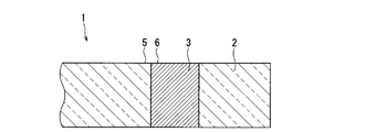
- FIG. 6 is a cross-sectional view showing an example of an edge portion of a through-hole type conductor portion and an edge portion of the conductor portion of the ceramic circuit board according to the embodiment.
- 5 is the edge of the through hole
- 6 is the edge of the conductor.
- the edge portion 5 of the through hole and the edge portion 6 of the conductor portion are flat surfaces that are continuously connected. For this reason, even if the surface roughness of the edge 5 of the through hole and the edge 6 of the conductor is measured continuously, Ra can be 1.0 ⁇ m or less and Rz can be 100 ⁇ m or less.
- mold conductor part may be sufficient. That is, it is a flat surface in which the edge of the concave portion and the edge of the concave conductor portion are connected. For this reason, even if the surface roughness of the edge of the concave portion and the edge of the concave conductor portion is continuously measured, Ra can be 1.0 ⁇ m or less and Rz can be 100 ⁇ m or less.
- the surface roughness Ra is 1.0 ⁇ m or less, and more preferably 0.5 ⁇ m or less.
- the maximum height Rz is 100 ⁇ m or less, and more preferably 30 ⁇ m or less. More preferably, the maximum height Rz is 10 ⁇ m or less.
- the lower limit of the surface roughness Ra is not particularly limited, but Ra is preferably 0.01 ⁇ m or more. Although it can be used even if Ra is less than 0.01 ⁇ m, polishing is essential for Ra to be 0.01 ⁇ m or less. If the polishing process is performed too much, the ceramic substrate is likely to fall off. When degranulation occurs, Rz may exceed 100 ⁇ m.
- the difference between the height of the edge of the recess of the ceramic substrate or the edge of the through hole and the height of the edge of the conductor is 0 ⁇ m or more and 5 ⁇ m or less. Either the edge of the recess (or the edge of the through hole) or the edge of the conductor may be higher. If the difference in height is larger than 5 ⁇ m, a step is formed, and the problem of dust adhesion is likely to occur.
- this state is a state in which the thickness of the ceramic substrate 2 and the thickness T of the through-hole type conductor portion 3 coincide.
- the difference in height between adjacent conductor portions is 0 ⁇ m or more and 5 ⁇ m or less.
- the conductor portions are arranged in pairs. If the height of adjacent conductor portions exceeds 5 ⁇ m, the semiconductor element is inclined obliquely. As long as Ra satisfies 1 ⁇ m or less and Rz satisfies 100 ⁇ m or less, the thickness T of the conductor portion may be larger than the thickness t of the ceramic substrate as shown in FIG.
- the shortest distance between adjacent conductor portions or through holes can be 2 mm or less, and further 1 mm or less.
- the minimum of the shortest distance of an adjacent conductor part or a through hole is not specifically limited, It is preferable that it is 0.5 mm or more. If the shortest distance between adjacent conductor portions or through holes is as short as less than 0.5 mm, processing when forming recesses or through holes becomes difficult.
- the filling rate of the conductor in the recess or the through hole is preferably 98% or more and 100% or less.
- the filling rate is less than 98%, it means that there are few conductors in the recessed conductor portion or the through-hole conductor portion.
- the number of conductors is small, there is a case where the amount of the conductor filled in the recess or the through hole is small. If the amount of conductor is small, there is a risk that a large step is formed between the edge of the recess (or the edge of the through hole) and the edge of the conductor. Further, when the step is small, there is a pore inside the conductor portion.
- the filling rate of the conductor in the recess or the through hole is preferably 98% or more and 100% or less, and more preferably 99% or more and 100% or less.
- the most preferable filling rate is 100%.
- the current carrying capacity can be increased by setting the filling factor of the conductor to 98% or more.
- the filling factor of the conductor may be less than 98%.
- X-ray CT imaging may be mentioned.
- the conductor and the cavity in the conductor part can be distinguished by image analysis.
- Cu, Al, Ag, and Au are elements that easily transmit X-rays.
- the filling rate can be measured in a non-destructive state by X-ray CT imaging.
- the diameter of the concave portion or the through hole is 1 mm or less.
- the diameter is preferably in the range of 0.1 to 0.3 mm (100 to 300 ⁇ m).
- the recessed conductor portions (or the through-hole conductor portions) are paired with each other and are electrically connected to the semiconductor element.
- Semiconductor devices are becoming smaller in size with higher output.
- the interval between the recessed conductor parts (or through-hole type conductor parts) is matched to the size of the semiconductor element. If the diameter is larger than 1 mm, the size of the semiconductor element may not be met.
- the ceramic circuit board according to the embodiment is suitable for mounting a flip chip type semiconductor element.
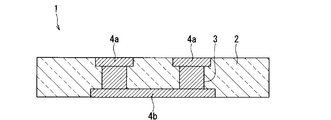
- FIG. 7 a structure in which the through-hole type conductive portion 3 and the recessed type conductive portions 4a and 4b are combined may be used. Moreover, it is good also as a structure which connected the back surface side as needed. Further, as shown in FIGS. 9 and 10, a structure in which the through-hole type conductor portion 3 and the recessed type conductive portions 4 and 4 are combined in an L shape may be employed.
- reference numeral 1 denotes a ceramic circuit board
- 3 denotes a through-hole type conductor portion
- 4 denotes a concave-type conductor portion.
- FIG. 10 shows a structure in which a cavity portion 8 is formed in the central axis direction of the through-hole type conductor portion 3.
- FIG. 9A is a cross-sectional view
- FIG. 9B is a top view.
- FIG. 10A is a cross-sectional view
- FIG. 10B is a top view.
- FIG. 10 shows a structure in which a hollow portion 8 is provided in the through-hole type conductor portion 3. This is a structure in which a conductor portion is provided on the inner surface of the through hole.
- the filling rate of the conductor in the through hole is less than 98%.
- the film density of the conductive film is preferably 98% or more.
- the conductor portion contains at least one selected from Cu, Al, Ag, and Au as a main component.
- These metals are highly conductive.
- the conductor portion can be easily formed by a plating method or a method of firing a metal paste. Therefore, the filling factor of the conductor in a small recessed part (or through hole) can be increased.
- “Containing as a main component” means a state in which a conductor is contained in an amount of 50% by mass or more and 100% by mass or less in the conductor part. For this reason, a conductor part shows at least 1 sort (s) selected from Cu, Cu alloy, Al, Al alloy, Ag, Ag alloy, Au, and Au alloy.
- the ceramic substrate is preferably one of an aluminum nitride substrate, a silicon nitride substrate, an aluminum oxide substrate, silicon carbide, silicon oxide, and zirconium oxide.
- the aluminum nitride substrate has a high thermal conductivity of 170 W / m ⁇ K or higher.
- the thermal conductivity can be 200 W / m ⁇ K or more.
- the three-point bending strength is about 300 to 450 MPa.
- a silicon nitride substrate having a thermal conductivity of 50 W / m ⁇ K or more.
- the upper limit of the thermal conductivity is 130 W / m ⁇ K or less.
- the three-point bending strength is as high as 600 MPa or more.
- the aluminum oxide substrate has a thermal conductivity of about 20 W / m ⁇ K, and a three-point bending strength of about 400 MPa.
- the silicon carbide substrate is used after being subjected to insulation treatment at a place where the conductive portion is provided.
- the zirconium oxide substrate has a three-point bending strength of about 400 to 500 MPa.
- AlN substrate An aluminum nitride substrate (AlN substrate) is characterized by high thermal conductivity. On the other hand, the strength is as low as 450 MPa or less. Therefore, the mainstream thickness of the substrate is about 0.635 mm.
- the silicon nitride substrate (Si 3 N 4 substrate) has a strength of 600 MPa or more, and further, a high value of 700 MPa or more. For this reason, the thickness of the substrate is not limited to 0.635 mm, and can be as thin as 0.32 mm or less.
- a silicon nitride substrate has a thermal conductivity of about half that of an AlN substrate, but the thickness of the substrate can be reduced, so that the thermal resistance is about the same. Since the silicon nitride substrate has high strength, the circuit substrate can be thinned.
- An aluminum oxide substrate (Al 2 O 3 substrate) has a low thermal conductivity, but is inexpensive.
- the material of the ceramic substrate is selected according to the purpose.
- a sintering aid is added to each ceramic substrate as necessary.
- Si 3 N 4 substrate when importance is attached to thinning and strength, it is preferable to use a Si 3 N 4 substrate.
- the conductive portion may be formed mainly of at least one selected from Cu, Al, Ag, and Au, and any one of an aluminum nitride substrate, a silicon nitride substrate, and an aluminum oxide substrate may be employed as the ceramic substrate.
- the ceramic substrate and the conductive portion are different in color, so that the position of the conductive portion can be easily detected by the CCD camera.
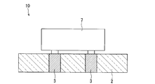
- the ceramic circuit board as described above is suitable for a semiconductor device in which a semiconductor element is mounted on a conductor portion.
- the semiconductor element include various elements such as a power element, a light emitting diode (LED), and a laser diode.
- the semiconductor element is mounted across the adjacent conductor portions. “Mounting across conductor portions” means mounting one semiconductor element using a pair of conductor portions. An example of such a semiconductor element is a flip chip type semiconductor element.
- the ceramic circuit board dust does not adhere to the step because the step between the edge of the recess (or through hole) of the ceramic substrate and the edge of the conductor is small. Further, since the difference in height between adjacent conductive portions is the same, when a semiconductor element is mounted across adjacent conductive portions (a pair of conductive portions), the semiconductor element can be mounted without being inclined. For example, in the case of an LED element, if there is an inclination of the element, a large influence appears on the light emission characteristics. Further, by arranging the semiconductor elements straight, it is possible to easily transfer the heat of the elements to the ceramic circuit board. Moreover, since a metal plate is not joined, the curvature of a ceramic circuit board can be suppressed. Further, since the metal plate is not bonded, no stress is generated at the bonding interface between the metal plate and the ceramic substrate, so that the heat cycle characteristics (TCT characteristics) are also excellent.
- TCT characteristics heat cycle characteristics
- a recessed conductive portion or a through-hole conductive portion can be provided at a place where a semiconductor element is desired to be mounted. For this reason, the freedom degree of module design can be raised.
- the metal plate is bonded to a portion that enters inside from the end of the ceramic substrate. Since it is necessary to ensure the creepage distance, a restriction is necessarily generated on the mounting position of the semiconductor element.
- the ceramic substrate is preferably one selected from an aluminum nitride substrate, a silicon nitride substrate, and an aluminum oxide substrate.
- the aluminum nitride substrate preferably has a thermal conductivity of 170 W / m ⁇ K or more and a three-point bending strength of 300 MPa or more.
- the silicon nitride substrate preferably has a thermal conductivity of 50 W / m ⁇ K or more and a three-point bending strength of 600 MPa or more.
- the aluminum oxide substrate preferably has a three-point bending strength of 350 MPa or more.
- the ceramic substrate preferably has a substrate thickness of 0.1 mm to 3.0 mm, more preferably 0.2 mm to 1.0 mm.
- the substrate thickness is preferably 0.60 mm or more.
- the substrate thickness is preferably less than 0.60 mm.
- the ceramic substrate may be one to which a sintering aid is added as necessary.
- a step of forming a recess or a through hole is performed. This process is performed by etching, blasting, laser processing, drilling, or the like. Moreover, it is preferable to provide a recessed part or a through hole by processing a ceramic substrate directly. There is also a method of processing the green sheet, but there is a possibility that the position of the recess or the through hole is shifted due to shrinkage due to sintering.
- the diameter of the recess or the through hole is preferably 1 mm or less.
- the diameter is preferably in the range of 0.1 to 0.3 mm. If the diameter is as small as less than 0.1 mm, processing is difficult. Further, if the diameter is larger than 1 mm, the size of the semiconductor element may be larger. Moreover, if the hole is excessively large, the strength of the ceramic substrate may be reduced.
- the conductor portion preferably contains at least one selected from Cu, Al, Ag, and Au as a main component.
- the plating method and the method of baking a metal paste are mentioned.
- the method of baking after inserting a metal pillar in a through hole and filling the clearance with the metal paste is also mentioned.
- the pressing step is preferably performed after performing a plating method or a method of firing a metal paste.
- the method of making a conductor part protrude from a ceramic substrate and performing a press process is preferable. By performing such a method, the pores in the conductor portion can be eliminated.
- the filling rate of the conductor in the recess or the through hole can be 98% or more, and further 100%.
- the pressing step can be performed by a pressing step using a flat plate or a mold. Moreover, you may press, heating. Examples of such processes include hot pressing and HIP (hot isostatic pressing).
- the surface roughness Ra of the ceramic circuit board can be made 1.0 ⁇ m or less, and further 0.5 ⁇ m or less.
- the maximum height Rz of the ceramic circuit board can be set to 100 ⁇ m or less, and further to 10 ⁇ m or less.
- the difference between the height of the edge of the recess (or the through hole) and the height of the edge of the conductor can be easily controlled to 0 ⁇ m or more and 5 ⁇ m or less. Further, the difference between the height of the edge of the recess (or through hole) and the height of the edge of the conductor may be adjusted by etching.
- a cleaning process shall be performed as necessary.
- the cleaning process is performed by air cleaning or the like. Since the ceramic circuit board according to the embodiment has a small step between the edge of the recess or the through hole and the edge of the conductive part, dust is difficult to adhere. Therefore, an effect that can be easily cleaned by air cleaning is obtained.
- Example 2 (Examples 1 to 10 and Comparative Examples 1 and 2) As a ceramic substrate, a silicon nitride substrate, an aluminum nitride substrate, and an aluminum oxide substrate shown in Table 1 below were prepared.
- the recesses or through holes shown in Table 2 were provided by laser processing.
- the recesses or through holes were provided in pairs so as to have the intervals shown in Table 2.
- the silicon nitride substrates 3 to 5 have a structure in which a recessed conductive portion and a through-hole conductive portion are combined as shown in FIG.
- conductive parts shown in Table 3 were formed.
- the conductive part was formed using Cu paste.
- Cu paste was filled in the recesses or through holes and baked. Thereafter, the upper and lower surfaces of the ceramic circuit board were pressed with a mold while heating the ceramic circuit board.
- ceramic circuit boards according to the respective examples were prepared. Moreover, the surface polishing process was implemented as needed.
- Comparative Example 1 the conductive portion protruded from the ceramic substrate. In Comparative Example 1, the pressing step and the polishing process were not performed.
- the surface roughness Ra and the maximum height Rz were measured. Moreover, the edge part of the recessed part or the through hole, and the edge part of the electroconductive part were measured continuously linearly. The results are shown in Table 4 below.
- Ra and Rz both have small values even when the edge of the concave portion or the through hole and the edge of the conductive portion are continuously measured. For this reason, it has been found that the level difference between the edge of the recess or the through hole and the edge of the conductive part is very small.
- the durability test was conducted by a TCT test (thermal cycle test).
- the thermal cycle was as follows: temperature-40 ° C. ⁇ 30 minutes hold ⁇ room temperature ⁇ 10 minutes hold ⁇ 150 ° C. ⁇ 30 minutes hold ⁇ room temperature ⁇ 10 minutes hold And the change rate of the curvature amount of the ceramic substrate after 1000 cycles and the incidence rate of defects such as cracks were measured.
- the amount of change in warpage is the amount of change relative to the warp before the test.
- the ease of dust removal was measured by measuring the ratio of dust remaining when the substrate surface was cleaned by air cleaning. That is, 100 ceramic circuit boards according to each example and comparative example were prepared. The percentage of dust remaining after cleaning for 1 minute at an air injection pressure of 0.25 MPa is shown.
- the ease of position detection with a CCD camera was conducted by implementing the process of mounting a semiconductor element 100 times while performing position detection with a CCD camera, and investigating the rate of occurrence of positional deviation.
- an aluminum nitride substrate (thermal conductivity 180 W / m ⁇ K, 3-point bending strength 400 MPa) bonded to a copper plate was prepared.
- the size of the aluminum nitride substrate was 50 mm long ⁇ 40 mm wide ⁇ 0.635 mm thick.
- the front side copper plate joined 10 mm long x 10 mm wide x 0.3 mm thick at intervals of 2 mm.
- a copper plate having a length of 45 mm, a width of 35 mm, and a thickness of 0.2 mm was joined as a back copper plate.
- the ceramic circuit boards according to the respective examples had a high dielectric breakdown voltage. This indicates that creeping discharge is sufficiently suppressed.
- those using a silicon nitride substrate had a high dielectric breakdown voltage.
Landscapes
- Engineering & Computer Science (AREA)
- Microelectronics & Electronic Packaging (AREA)
- Chemical & Material Sciences (AREA)
- Ceramic Engineering (AREA)
- Inorganic Chemistry (AREA)
- Printing Elements For Providing Electric Connections Between Printed Circuits (AREA)
- Structure Of Printed Boards (AREA)
Abstract
凹部およびスルーホールの少なくとも一方を有するセラミックス回路基板において、上記凹部またはスルーホール内には導体が充填された導体部を有し、上記セラミックス回路基板の表面粗さRaが1.0μm以下であり、最大高さRzが100μm以下であることを特徴とするセラミックス回路基板である。また、最大高さRzが10μm以下であることが好ましい。また、表面粗さRaが0.5μm以下であることが好ましい。上記構成によれば、半導体素子を実装する導電部の位置決め性が優れたセラミックス回路基板を提供することができる。
Description
後述する実施形態は、セラミック回路基板およびそれを用いた半導体装置に関する。
セラミックス回路基板は、半導体素子を搭載する基板として用いられている。半導体素子は、パワー素子、発光ダイオード(LED)、レーザダイオードなど様々なものが挙げられる。従来のセラミックス回路基板は、セラミックス基板上に金属板を接合して形成されている。具体的には、金属板/セラミックス基板/金属板となるように素材を積層した構造を有している。このような積層構造とした場合、セラミックス基板と金属板との熱膨張率の差からセラミックス回路基板に反りが生じ易い問題点があった。
一方で、半導体素子は、年々高出力化している。これに伴い動作補償温度(ジャンクション温度)が高くなっている。第7世代の半導体では動作補償温度が150℃になり、第8世代では175℃以上になると言われている。このため、構成材料の熱膨張率の差に起因してセラミックス回路基板の耐熱サイクル特性が低下する問題点もあった。
また、セラミックス基板にスルーホールを設け、このスルーホールによりセラミックス回路基板の表裏の導通を図る構造も採用されている。
例えば、特開2006-287126号公報(特許文献1)には、スルーホールにより導通を図る構造が開示されている。特許文献1はLEDを搭載するためのセラミックス回路基板である。
特許文献1のようにスルーホール型セラミックス回路基板であると、金属板を接合しないため反りの発生を抑制することができる。その一方、特許文献1のセラミックス回路基板は、LEDチップを搭載する部分を凸状にしているので、セラミックス基板を凸状に研磨することは、コスト的負荷が大きい。また、特許文献1のセラミックス回路基板では、スルーホール表面に配線パターンを設けた後、半田付けにてLEDチップを実装している。
スルーホール表面上の配線パターンの厚さは、通常50μm程度である。この配線パターンは、例えばCuメッキしたものをエッチング加工してパターニングする。このため、配線パターンには段差ができ易い。その段差にダストなどが付着すると、ショート(短絡)が発生し易くなり、デバイスの不具合が発生し易い。また、付着したダストが段差間に入ると、除去しにくいという問題があった。
本発明は、このような課題に対応するためのものであり、耐熱サイクル特性を向上させると共に、配線パターンにゴミが付着したとしても除去し易いセラミックス回路基板を提供することを目的とする。
実施形態に係るセラミックス回路基板は、凹部およびスルーホールの少なくとも一方を有するセラミックス回路基板において、上記凹部またはスルーホール内には導体が充填された導体部を有し、上記セラミックス回路基板の表面粗さRaが1.0μm以下であり、最大高さRzが100μm以下であることを特徴とするものである。
実施形態に係るセラミックス回路基板は、凹部およびスルーホールの少なくとも一方を有するセラミックス回路基板において、上記凹部またはスルーホール内には導体が充填された導体部を有し、上記セラミックス回路基板の表面粗さRaが1.0μm以下であり、最大高さRzが100μm以下であることを特徴とするものである。
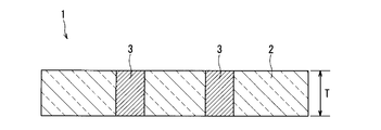
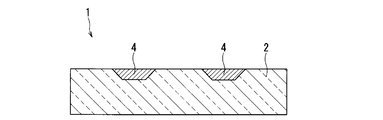
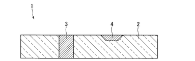
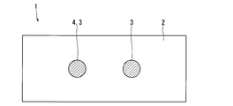
図1~5に各実施形態に係るセラミックス回路基板の一例を示す。図1~5において、符号1はセラミックス回路基板であり、2はセラミックス基板であり、3はスルーホール型導体部であり、4は凹部型導体部、である。図1および図2は、スルーホール型導体部を有する構造を示す。また、図3は凹部型導体部を有する構造を示す。また、図4はスルーホール型導体部と凹部型導体部とを共に有する構造を示す。また、図5はセラミックス回路基板1の上面図である。
実施形態に係るセラミックス回路基板は、凹部およびスルーホールの少なくとも一方を有している。スルーホールは図1に示したように、セラミックス基板の表裏に貫通した孔である。図1では直線形状の孔としているが、曲線形状または段差形状の孔であってもよい。また、三角形を上下に合わせたような形状、すなわち断面がX字形状のスルーホールであってもよい。また、凹部は、図3に示すように、セラミックス基板を貫通していない構造を有してもよい。図3においては、セラミックス基板の表面側に広くなっている形状(台形形状)としたが、断面四角形状であってもよい。また、図4は凹部とスルーホールとの両方を有する構造を示す。
また、図5は、実施形態に係るセラミックス回路基板の一例を示す上面図である。図5では凹部またはスルーホールの上面形状を円形に設定している。なお、上面形状は円形に限らず、四角形状、楕円形状、湾曲形状など様々な形状で構成してもよい。
凹部またはスルーホール内には、導体を充填した導体部が形成されている。スルーホール内に充填された導体部はスルーホール型導体部となる。また、凹部内に充填された導体部は凹部型導体部となる。導体部は半導体素子と導通をとるための配線となる。半導体素子は、一対の導体部により導通を図られる。図1~5は、一対の導体部を有する構造として例示している。複数の半導体素子を搭載する場合は、その数に対応して導体部を増加させる。
また、セラミックス回路基板の表面粗さRaが1.0μm以下であり、最大高さRzが100μm以下であることを特徴とするものである。Ra、RzはJIS-B-0601(2013)に定められたものである。つまり、表面粗さRaは算術平均粗さのことである。また、最大高さRzは最大高さ粗さのことである。
実施形態に係るセラミックス回路基板は、導体部が設けられた表面の任意の箇所のRaおよびRzを測定したとしても、Raが1.0μm以下、Rzが100μm以下となる。
図6は、実施形態に係るセラミックス回路基板のスルーホール型導体部の縁部と導体部の縁部の一例を示す断面図である。図中、5はスルーホールの縁部、6は導体部の縁部、である。図6は、スルーホールの縁部5と導体部の縁部6とは、連続して繋がった平坦面となっている。このため、スルーホールの縁部5と導体部の縁部6とを連続的に表面粗さを測定したとしても、Raを1.0μm以下とし、Rzを100μm以下とすることができる。
なお、図6ではスルーホール型導体部を使ったものを例示したが、凹部型導体部であってもよい。つまり、凹部の縁部と凹部型導体部の縁部がつながった平坦面となっている。このため、凹部の縁部と凹部型導体部の縁部を連続的に表面粗さを測定したとしてもRaを1.0μm以下とし、Rzを100μm以下とすることができる。
このような構造を採用することにより、導体部とセラミックス基板との境界に大きな段差がされない。このため、導体部間にダストが付着し難い。また、ダストが付着したとしても、エアーの噴き付けなどの簡単な清掃工程で除去することが可能である。
また、表面粗さRaは1.0μm以下であり、さらには0.5μm以下であることが好ましい。また、最大高さRzは100μm以下であり、さらには30μm以下であることが好ましい。さらに好ましくは最大高さRzが10μm以下である。RaやRzが小さい平坦面とすることにより、導体部がCCDカメラによって位置検出し易くなる。導体部の位置検出が容易になると、半導体素子の実装工程中における実装エラーが大幅に抑制される。
また、表面粗さRaの下限値は特に限定されるものではないが、Raは0.01μm以上であることが好ましい。Raが0.01μm未満であっても使用可能ではあるが、Raを0.01μm以下にするには研磨加工が必須である。研磨加工を施し過ぎると、セラミックス基板の脱粒が起き易くなる。脱粒がおきるとRzが100μmを超えるおそれがある。
また、セラミックス基板の凹部の縁部またはスルーホールの縁部の高さと導体部の縁部の高さとの差が0μm以上5μm以下であることが好ましい。凹部の縁部(またはスルーホールの縁部)と導体部の縁部は、どちらが高くても良い。高さの差が5μmを超えて大きいと、段差が出来てしまう結果、ダストの付着という問題が生じ易くなる。
また、セラミックス基板のスルーホールの縁部(または凹部の縁部)の高さと導体部の縁部の高さの差が0μmの状態が最も好ましい。この状態は図1に示したように、セラミックス基板2の厚さとスルーホール型導体部3の厚さTが一致した状態である。
また、隣り合う導体部の高さの差が0μm以上5μm以下であることが好ましい。後述するようにフリップチップ型半導体素子を搭載する場合には、導体部をペアにして配置される。隣り合う導体部の高さが5μmを超えて大きいと、半導体素子が斜めに傾いた状態となってしまう。また、Raが1μm以下、Rzが100μm以下を満たすのであれば、図2に示したように導体部の厚さTがセラミックス基板の厚さtより大きくなっても良い。
また、このような形状とすることにより、沿面放電を抑制することができる。そのため、隣り合う導体部またはスルーホールの最短距離を2mm以下、さらには1mm以下にすることができる。なお、隣り合う導体部またはスルーホールの最短距離の下限は特に限定されるものではないが、0.5mm以上であることが好ましい。隣り合う導体部またはスルーホールの最短距離が0.5mm未満と短くなると、凹部やスルーホールを形成する際の加工が困難になる。
また、凹部またはスルーホール内の導体の充填率は98%以上100%以下であることが好ましい。充填率が98%未満であると、凹部型導体部またはスルーホール型導体部の中の導体が少ないことを意味する。導体が少ない場合としては、凹部またはスルーホール内に充填された導体量が少ない場合が挙げられる。導体量が少ないと、凹部の縁部(またはスルーホールの縁部)と導体部の縁部の間に大きな段差が出来てしまうおそれがある。また、段差が小さな場合、導体部の内部にポアがある状態となる。導体部の内部にポアがあると、導体部による通電容量を確保できなくなるおそれがある。このため、凹部またはスルーホール内の導体の充填率は98%以上100%以下、さらには99%以上100%以下が好ましい。また、最も好ましい充填率は100%である。
また、導体の充填率を98%以上にすることにより通電容量を高くすることができる。これにより、大電流が必要な半導体素子に好適なセラミックス回路基板とすることができる。
言い換えると、大電流が不要な半導体素子を搭載する場合は、導体の充填率は98%未満であっても良い。このような場合は、後述する図10に示したように、スルーホール型導体部3の中に空洞部8を設けた構造とすることが好ましい。つまり、スルーホール内面のみに導体膜として導体部を設けた構造である。導体膜によって形成された導体部であったとしても、導体膜の膜密度は98%以上であることが好ましい。
言い換えると、大電流が不要な半導体素子を搭載する場合は、導体の充填率は98%未満であっても良い。このような場合は、後述する図10に示したように、スルーホール型導体部3の中に空洞部8を設けた構造とすることが好ましい。つまり、スルーホール内面のみに導体膜として導体部を設けた構造である。導体膜によって形成された導体部であったとしても、導体膜の膜密度は98%以上であることが好ましい。
また、凹部またはスルーホール内の導体の充填率の測定方法は、X線CT撮影が挙げられる。X線CT撮影であれば、画像解析により導体部内の導体と空洞が区別できる。また、Cu、Al、Ag、AuはX線を透過し易い元素である。後述するように、導体部をCu、Al、Ag、Auから選ばれる少なくとも1種を主成分とすることにより、X線CT撮影により充填率を非破壊状態で測定することが可能である。
また、凹部またはスルーホールの直径が1mm以下であることが好ましい。また、直径は0.1~0.3mm(100~300μm)の範囲が好ましい。前述のように、凹部型導体部(またはスルーホール型導体部)は一対(ペア)となって半導体素子と導通を図ることになる。半導体素子は、高出力化と共に小型化も進行している。例えば、フリップチップ型半導体素子の場合、凹部型導体部(またはスルーホール型導体部)同士の間隔を半導体素子のサイズに合わせることになる。直径が1mmより大きいと、半導体素子のサイズに合わなくなるおそれがある。直径1mm以下と小さな凹部型導体部またはスルーホール型導体部のときに、導体部の内部にポアがあると、通電容量を確保出来なくなる。このため、実施形態に係るセラミックス回路基板は、フリップチップ型半導体素子を実装するのに好適なものであると言える。
また、図7に示すように、スルーホール型導電部3と凹部型導電部4a,4bとを組合せた構造であっても良い。また、必要に応じ、裏面側をつなげた構造としても良い。また、図9および図10に示したように、スルーホール型導体部3と凹部型導電部4,4とをL字に組合せた構造を採用しても良い。図中、符号1はセラミックス回路基板、3はスルーホール型導体部、4は凹部型導体部、である。また、図10はスルーホール型導体部3の中心軸方向に空洞部8を形成した構造を示す。また、図9(a)は断面図であり、図9(b)は上面図である。また、図10(a)は断面図であり、図10(b)は上面図である。
図10はスルーホール型導体部3の中に空洞部8を設けた構造を示す。これはスルーホール内面に導体部を設けた構造である。図10に示す構造の場合、スルーホール内の導体の充填率は98%未満になる。この場合は、導電膜の膜密度を98%以上にすることが好ましい。
また、導体部は、Cu、Al、Ag、Auから選択される少なくとも1種を主成分とすることが好ましい。これら金属は導電性が高い。また、メッキ法や金属ペーストを焼成する方法によって導体部を形成し易い利点がある。そのため、小さな凹部(またはスルーホール)内における導体の充填率を高くすることができる。なお、「主成分とする」とは導体部の中に導体が50質量%以上100質量%以下含有される状態を示す。このため、導体部はCu、Cu合金、Al、Al合金、Ag、Ag合金、Au、Au合金から選択される少なくとも1種を示すものである。
また、セラミックス基板は、窒化アルミニウム基板、窒化珪素基板、酸化アルミニウム基板、炭化ケイ素、酸化ケイ素、酸化ジルコニウムのいずれか1種であることが好ましい。
ここで、窒化アルミニウム基板は、熱伝導率が170W/m・K以上と高い。また、熱伝導率は200W/m・K以上とすることも可能である。また、3点曲げ強度は300~450MPa程度である。
また、窒化珪素基板は、熱伝導率が50W/m・K以上のものを使用する。また、熱伝導率の上限は130W/m・K以下である。また、3点曲げ強度は600MPa以上と高い。
また、酸化アルミニウム基板は、熱伝導率が20W/m・K程度であり、3点曲げ強度は400MPa程度である。また、炭化ケイ素基板は導電部を設ける箇所に絶縁処理した後に使用する。また、酸化ジルコニウム基板は3点曲げ強度が400~500MPa程度である。
窒化アルミニウム基板(AlN基板)は、熱伝導率が高いのが特徴である。その一方で強度は450MPa以下と低い。そのため基板の厚さは0.635mm程度が主流となる。
窒化珪素基板(Si3N4基板)は、強度が600MPa以上であり、さらには700MPa以上と高い。このため、基板の厚さは0.635mmに限らず、0.32mm以下と薄くすることができる。窒化珪素基板は、AlN基板と比べて熱伝導率が半分程度であるが、基板の厚さを薄くできるので、熱抵抗は同程度である。窒化珪素基板は強度が高いため、回路基板の薄型化が可能である。
また、酸化アルミニウム基板(Al2O3基板)は、熱伝導率は低いが、価格は安い。セラミックス基板の材質は、それぞれ目的に合わせて選択するものとする。また、それぞれのセラミックス基板には、必要に応じ焼結助剤を添加するものとする。なお、熱伝導率を重視する場合には、AlN基板を用いることが好ましい。また、薄型化や強度を重視する場合はSi3N4基板を用いることが好ましい。
また、導電部をCu、Al、Ag、Auから選択される少なくとも1種を主成分として形成し、セラミックス基板を窒化アルミニウム基板、窒化珪素基板、酸化アルミニウム基板のいずれか1種を採用することが好ましい。この組合せであると、セラミックス基板と導電部との色が異なるので、CCDカメラによる導電部の位置検出が容易となる。
以上のようなセラミックス回路基板は、導体部上に半導体素子を実装する半導体装置に好適である。半導体素子としては、パワー素子、発光ダイオード(LED)、レーザダイオードなど様々な素子が挙げられる。また、半導体素子は隣り合う導体部をまたいで実装されていることが好ましい。「導体部をまたいで実装する」とは、一対の導体部を使用して一つの半導体素子を実装することである。このような半導体素子としてはフリップチップ型半導体素子が挙げられる。
実施形態に係るセラミックス回路基板は、セラミックス基板の凹部(またはスルーホール)の縁部と導体部の縁部との段差が小さいため、段差にダストが付着しない。また、隣り合う導電部の高さの差を同一にしてあるため、隣り合う導電部(一対の導電部)をまたいで半導体素子を搭載したときに、半導体素子を傾斜させずに実装できる。例えば、LED素子の場合、素子の傾きがあると発光特性に大きな影響が出現する。また、半導体素子をまっすぐに配置することにより、素子の熱をセラミックス回路基板に伝達し易くすることができる。また、金属板を接合しないため、セラミックス回路基板の反りを抑制できる。また、金属板を接合していないため、金属板とセラミックス基板の接合界面に応力が発生しないので耐熱サイクル特性(TCT特性)も優れている。
また、凹部型導電部またはスルーホール型導電部の数を増加させることにより、複数の半導体素子を実装することが可能である。また、半導体素子を実装したい場所に、凹部型導電部またはスルーホール型導電部を設けることができる。このため、モジュール設計の自由度を高めることができる。例えば、金属板を接合したセラミックス回路基板の場合、セラミックス基板の端部から内側に入った箇所に金属板を接合することになる。沿面距離を確保する必要があるため、半導体素子の実装位置に制約が必然的に生じる。
次に実施形態に係るセラミックス回路基板の製造方法について説明する。実施形態に係るセラミックス回路基板は上記構成を有していれば、その製造方法は特に限定されるものではない。
まず、セラミックス基板を用意する。セラミックス基板は、窒化アルミニウム基板、窒化珪素基板、酸化アルミニウム基板から選択される1種が好ましい。また、窒化アルミニウム基板は、熱伝導率が170W/m・K以上であり、かつ3点曲げ強度が300MPa以上のものが好ましい。また、窒化珪素基板は、熱伝導率が50W/m・K以上であり、かつ、3点曲げ強度が600MPa以上のものが好ましい。また、酸化アルミニウム基板は、3点曲げ強度が350MPa以上のものが好ましい。
また、セラミックス基板は、基板厚さが0.1mm以上3.0mm以下、さらには0.2mm以上1.0mm以下であることが好ましい。基板強度が500MPa未満の場合は、基板厚さは0.60mm以上が好ましい。また、基板強度が500MPa以上の場合は、基板厚さは0.60mm未満が好ましい。また、セラミックス基板は、必要に応じ焼結助剤を添加したものであってもよい。
次に、凹部またはスルーホールを形成する工程を行う。この工程は、エッチング加工、ブラスト加工、レーザ加工、ドリルでの加工などで実施される。また、セラミックス基板を直接加工して凹部またはスルーホールを設けることが好ましい。グリーンシートを加工する方法もあるが、焼結による収縮により凹部またはスルーホールの位置がずれる可能性がある。
また、凹部またはスルーホールの直径は1mm以下が好ましい。また、直径は0.1~0.3mmの範囲が好ましい。直径が0.1mm未満と小さいと、加工が難しい。また、直径が1mmより大きいと、半導体素子のサイズより大きくなってしまうおそれがある。また、あまり過大な穴をあけるとセラミックス基板の強度が低下するおそれがある。
次に導体部を形成する工程を実施する。導体部は、Cu、Al、Ag、Auから選択される少なくとも1種を主成分とすることが好ましい。また、導体部の形成方法としては、メッキ法や金属ペーストを焼成する方法が挙げられる。また、スルーホールに金属柱を挿入し、その隙間に金属ペーストを充填した後、焼成する方法も挙げられる。
また、必要に応じ、押圧工程を実施しても良い。押圧工程は、メッキ法や金属ペーストを焼成する方法を行った後に、実施することが好ましい。また、導体部をセラミックス基板からはみ出させて、押圧工程を行う方法が好ましい。このような方法を行うことにより、導体部中のポアを消滅させることができる。また、凹部またはスルーホール内の導体の充填率を98%以上、さらには100%とすることができる。また、押圧工程は、平板や金型によるプレス工程でも実施できる。また、加熱しながら押圧してもよい。このような工程としては、ホットプレス、HIP(熱間静水圧プレス)などが挙げられる。
また、必要に応じ、押圧工程を実施しても良い。押圧工程は、メッキ法や金属ペーストを焼成する方法を行った後に、実施することが好ましい。また、導体部をセラミックス基板からはみ出させて、押圧工程を行う方法が好ましい。このような方法を行うことにより、導体部中のポアを消滅させることができる。また、凹部またはスルーホール内の導体の充填率を98%以上、さらには100%とすることができる。また、押圧工程は、平板や金型によるプレス工程でも実施できる。また、加熱しながら押圧してもよい。このような工程としては、ホットプレス、HIP(熱間静水圧プレス)などが挙げられる。
また、必要に応じ、研磨加工工程を実施しても良い。研磨加工により、セラミックス回路基板の表面粗さRaを1.0μm以下、さらには0.5μm以下にすることができる。同様に、セラミックス回路基板の最大高さRzを100μm以下、さらには10μm以下にすることができる。
また、上記研磨加工を実施することにより、凹部(またはスルーホール)の縁部の高さと導体部の縁部の高さとの差を0μm以上5μm以下に制御し易くなる。また、エッチング加工により、凹部(またはスルーホール)の縁部の高さと導体部の縁部の高さとの差を調整しても良い。
また、必要に応じ、クリーニング工程を実施するものとする。クリーニング工程は、エアー洗浄などで実施される。実施形態に係るセラミックス回路基板は、凹部またはスルーホールの縁部と導電部の縁部との段差が小さいので、ダストが付着し難い。そのため、エアー洗浄で容易にクリーニングできる効果が得られる。
(実施例)
(実施例1~10および比較例1~2)
セラミックス基板として、下記表1に示す窒化珪素基板、窒化アルミニウム基板、酸化アルミニウム基板を用意した。

(実施例1~10および比較例1~2)
セラミックス基板として、下記表1に示す窒化珪素基板、窒化アルミニウム基板、酸化アルミニウム基板を用意した。
次に、レーザ加工により、表2に示す凹部またはスルーホールを設けた。凹部またはスルーホールは、表2に示した間隔となるようにペアで設けた。また、窒化珪素基板3~5は図9に示したような凹部型導電部とスルーホール型導電部とを組合せた構造である。

次に、表3に示す導電部を形成した。導電部はCuペーストを用いて形成した。Cuペーストを凹部またはスルーホール内に充填し、焼成した。その後、セラミックス回路基板を加熱しながら、その上下面を金型で押圧した。これにより各実施例に係るセラミックス回路基板を用意した。また、必要に応じ、表面研磨加工を実施した。
また、比較例1は、セラミックス基板から導電部が突出した構造とした。また、比較例1は押圧工程および研磨加工を実施しなかったものである。
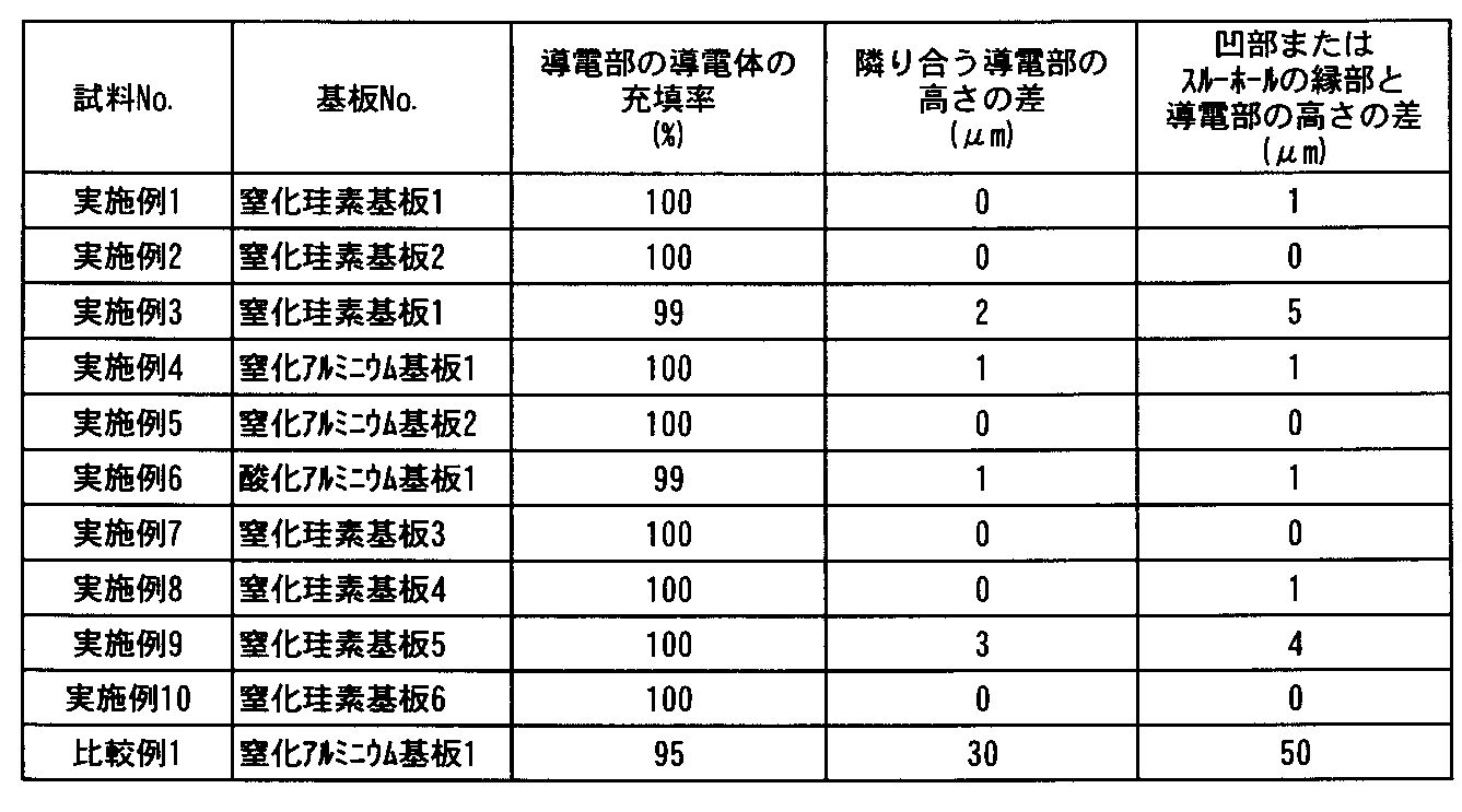
実施例および比較例に係るセラミックス回路基板において、表面粗さRa、最大高さRzを測定した。また、凹部またはスルーホールの縁部と導電部の縁部とを直線状に連続して測定した。その結果を下記表4に示す。

各実施例に係るセラミックス回路基板は、凹部またはスルーホールの縁部と導電部の縁部とを連続して測定したとしても、Ra、Rzが共に小さな値となった。このため、凹部またはスルーホールの縁部と導電部の縁部との段差が非常に小さいことが判明した。
次に、各実施例および比較例に係るセラミックス回路基板の耐久性試験、ダスト除去の容易性、CCDカメラによる導電部の位置検出容易性を調査した。
耐久性試験は、TCT試験(熱サイクル試験)により実施した。熱サイクルは、温度-40℃×30分間保持→室温×10分間保持→150℃×30分間保持→室温×10分間保持を1サイクルとした。そして、1000サイクル後のセラミックス基板の反り量の変化率、割れなどの不具合の発生率を測定した。反りの変化量は、試験前の反りに対しての変化量である。
ダスト除去の容易性は、エアー洗浄にて、基板表面を洗浄したとき、ダストが残存した割合を測定した。すなわち、各実施例および比較例に係るセラミックス回路基板をそれぞれ100枚用意した。エアー噴射圧0.25MPaにて1分間クリーニングした後にダストが残存したものの割合を示した。
CCDカメラによる位置検出容易性は、CCDカメラで位置検出を行いながら半導体素子を実装する工程を100回実施し、位置ずれが発生した割合を調査した。
また、比較例2として、窒化アルミニウム基板(熱伝導率180W/m・K、3点曲げ強度400MPa)に銅板を接合したものを用意した。窒化アルミニウム基板のサイズは縦50mm×横40mm×厚さ0.635mmとした。また、表側銅板は縦10mm×横10mm×厚さ0.3mmのものを2mm間隔で接合した。また、裏銅板として、縦45mm×横35mm×厚さ0.2mmの銅板を接合した。
各測定結果を下記表5に示す。
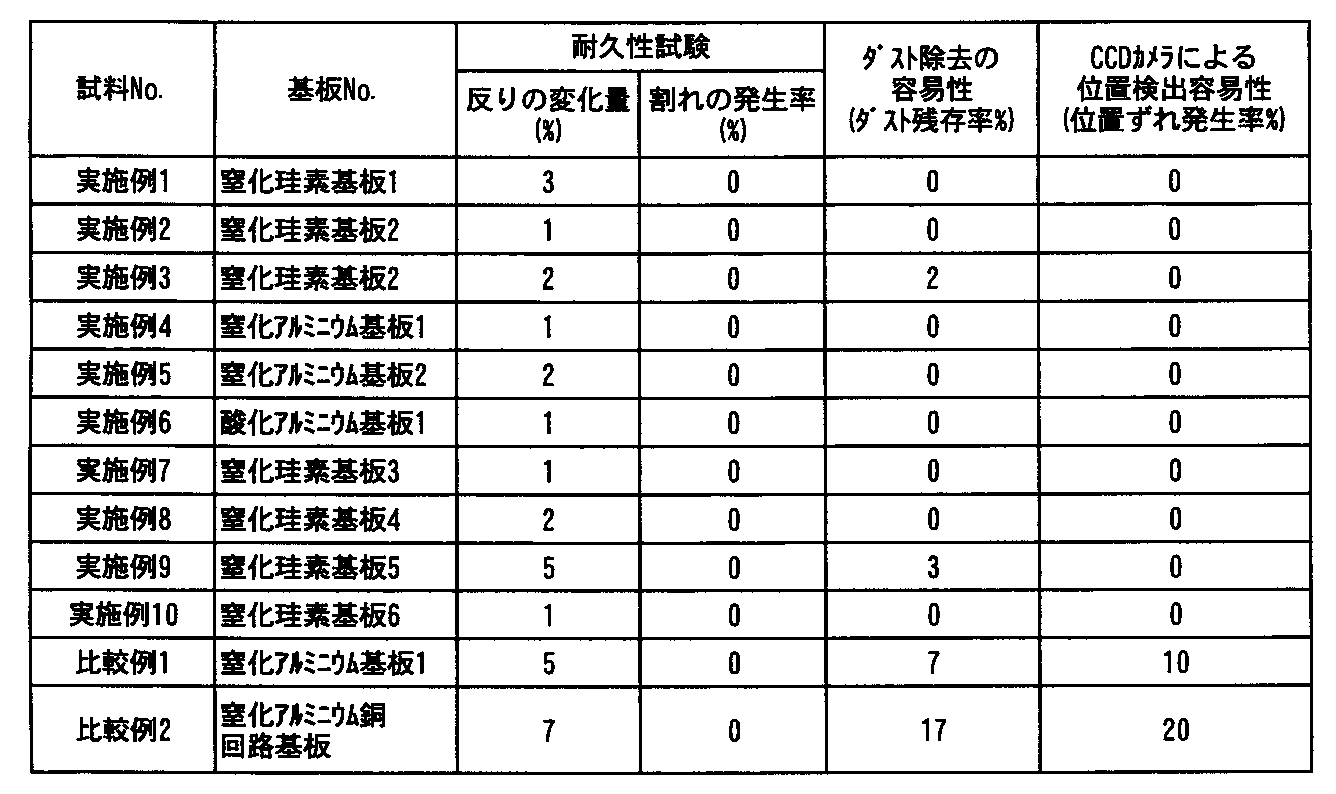
上記表5に示す結果から明らかなように、各実施例に係るセラミックス回路基板は優れた特性を示した。それに対して、比較例1は段差が大きいためダスト除去性能および位置検出性能が共に低下した。また、比較例2のように銅板を接合したセラミックス回路基板も特性が低下した。
次に、各実施例および比較例に係るセラミックス回路基板に対し、沿面放電の影響を調査した。それぞれの導体部(スルーホール)に交流電圧(50Hz)を印加して、絶縁破壊した電圧を測定した。その測定結果を下記表6に示す。
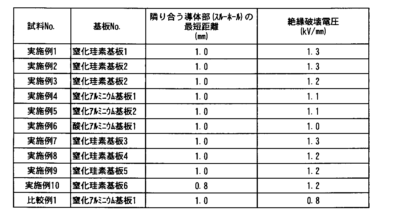
上記表6に示す結果から明らかなように、各実施例に係るセラミックス回路基板は絶縁破壊電圧が大きかった。これは沿面放電が十分に抑制されていることを示す。特に、窒化珪素基板を用いたものは絶縁破壊電圧が高かった。
それに対し、比較例1のように凹部またはスルーホールの縁部と導電部の高さの差が大きいと絶縁破壊電圧が小さくなった。導体部の突出高さが大きくなることにより、パターン間の異物や表面汚染が除去しきれず、沿面放電が起き易いことを示している。
以上、本発明のいくつかの実施形態を例示したが、これらの実施形態は、例として提示したものであり、発明の範囲を限定することは意図していない。これら新規な実施形態は、その他の様々な形態で実施されることが可能であり、発明の要旨を逸脱しない範囲で、種々の省略、置き換え、変更などを行うことができる。これら実施形態やその変形例は、発明の範囲や要旨に含まれるとともに、特許請求の範囲に記載された発明とその均等の範囲に含まれる。また、前述の各実施形態は、相互に組み合わせて実施することができる。
1…セラミックス回路基板
2…セラミックス基板
3…スルーホール型導体部
4,4a,4b…凹部型導体部
5…スルーホールの縁部
6…導体部の縁部
7…半導体素子
8…空洞部
10…半導体装置
T…スルーホール型導体部の厚さ
t…セラミックス基板の厚さ
2…セラミックス基板
3…スルーホール型導体部
4,4a,4b…凹部型導体部
5…スルーホールの縁部
6…導体部の縁部
7…半導体素子
8…空洞部
10…半導体装置
T…スルーホール型導体部の厚さ
t…セラミックス基板の厚さ
Claims (11)
- 凹部およびスルーホールの少なくとも一方を有するセラミックス回路基板において、上記凹部またはスルーホール内には導体が充填された導体部を有し、上記セラミックス回路基板の表面粗さRaが1.0μm以下であり、最大高さRzが100μm以下であることを特徴とするセラミックス回路基板。
- 前記最大高さRzが10μm以下であることを特徴とする請求項1記載のセラミックス回路基板。
- 前記表面粗さRaが0.5μm以下であることを特徴とする請求項1または請求項2記載のセラミックス回路基板。
- 前記凹部またはスルーホール内の導体の充填率が98%以上100%以下であることを特徴とする請求項1ないし請求項3のいずれか1項に記載のセラミックス回路基板。
- 隣り合う導体部の高さの差が0μm以上5μm以下であることを特徴とする請求項1ないし請求項4のいずれか1項に記載のセラミックス回路基板。
- 前記セラミックス基板のスルーホール縁部の高さと導体部の縁部の高さとの差が0μm以上5μm以下であることを特徴とする請求項1ないし請求項5のいずれか1項に記載のセラミックス回路基板。
- 前記スルーホールの直径が1mm以下であることを特徴とする請求項1ないし請求項6のいずれか1項に記載のセラミックス回路基板。
- 前記セラミックス基板は、窒化アルミニウム、窒化珪素、酸化アルミニウム、炭化ケイ素、酸化ケイ素、酸化ジルコニウムのいずれか1種を含む基板であることを特徴とする請求項1ないし請求項7のいずれか1項に記載のセラミックス回路基板。
- 前記導体部は、Cu、Al、Ag、Auから選択される少なくとも1種を主成分とすることを特徴とする請求項1ないし請求項8のいずれか1項に記載のセラミックス回路基板。
- 請求項1ないし請求項9のいずれか1項に記載のセラミックス回路基板の導体部上に半導体素子を実装したことを特徴とする半導体装置。
- 前記半導体素子は隣り合う導体部をまたいで実装されていることを特徴とする請求項10記載の半導体装置。
Priority Applications (2)
| Application Number | Priority Date | Filing Date | Title |
|---|---|---|---|
| JP2018508976A JP6833818B2 (ja) | 2016-03-29 | 2017-03-14 | セラミック回路基板およびそれを用いた半導体装置 |
| US16/082,526 US10674603B2 (en) | 2016-03-29 | 2017-03-14 | Ceramic circuit board and semiconductor device using the same |
Applications Claiming Priority (2)
| Application Number | Priority Date | Filing Date | Title |
|---|---|---|---|
| JP2016-065757 | 2016-03-29 | ||
| JP2016065757 | 2016-03-29 |
Publications (1)
| Publication Number | Publication Date |
|---|---|
| WO2017169749A1 true WO2017169749A1 (ja) | 2017-10-05 |
Family
ID=59965247
Family Applications (1)
| Application Number | Title | Priority Date | Filing Date |
|---|---|---|---|
| PCT/JP2017/010259 Ceased WO2017169749A1 (ja) | 2016-03-29 | 2017-03-14 | セラミック回路基板およびそれを用いた半導体装置 |
Country Status (3)
| Country | Link |
|---|---|
| US (1) | US10674603B2 (ja) |
| JP (1) | JP6833818B2 (ja) |
| WO (1) | WO2017169749A1 (ja) |
Cited By (3)
| Publication number | Priority date | Publication date | Assignee | Title |
|---|---|---|---|---|
| WO2021210395A1 (ja) * | 2020-04-14 | 2021-10-21 | 学校法人関西学院 | 窒化アルミニウム基板の製造方法、窒化アルミニウム基板、及び、レーザー加工により窒化アルミニウム基板に導入された歪層を除去する方法 |
| JP2022512336A (ja) * | 2018-12-10 | 2022-02-03 | ティーディーケイ・エレクトロニクス・アクチェンゲゼルシャフト | 基板及び基板の製造方法 |
| WO2022201571A1 (ja) * | 2021-03-22 | 2022-09-29 | 富士フイルムビジネスイノベーション株式会社 | 発光装置及び計測装置 |
Families Citing this family (4)
| Publication number | Priority date | Publication date | Assignee | Title |
|---|---|---|---|---|
| CN111372382B (zh) * | 2020-04-15 | 2021-05-25 | 黄石广合精密电路有限公司 | 一种pcb板的子母板压合对位设计工艺方法 |
| US20230070377A1 (en) * | 2021-09-09 | 2023-03-09 | Onano Industrial Corp. | Integrated structure of circuit mold unit of ltcc electronic device |
| US20230307314A1 (en) * | 2022-03-24 | 2023-09-28 | Texas Instruments Incorporated | Direct bond copper substrate with metal filled ceramic substrate indentations |
| TWI818870B (zh) * | 2023-02-17 | 2023-10-11 | 華碩電腦股份有限公司 | 隔熱墊以及具有該隔熱墊之電子裝置 |
Citations (9)
| Publication number | Priority date | Publication date | Assignee | Title |
|---|---|---|---|---|
| JPS63216398A (ja) * | 1987-03-05 | 1988-09-08 | ジエコ−株式会社 | 回路基板の製造方法 |
| JPH03102893A (ja) * | 1989-09-18 | 1991-04-30 | Tokuyama Soda Co Ltd | プリント配線板の製造方法 |
| JPH03276790A (ja) * | 1990-03-27 | 1991-12-06 | Mitsubishi Materials Corp | スルーホールを有する回路基板 |
| JPH03283590A (ja) * | 1990-03-30 | 1991-12-13 | Nec Corp | セラミック基板の製造方法 |
| JPH09219577A (ja) * | 1996-02-09 | 1997-08-19 | Nikko Co | セラミック配線板の製造方法 |
| JP2002319758A (ja) * | 2001-04-20 | 2002-10-31 | Murata Mfg Co Ltd | セラミック回路基板及びその製造方法 |
| JP2006005252A (ja) * | 2004-06-18 | 2006-01-05 | Nandei Electronics:Kk | 回路基板及びその製造方法 |
| JP2006287126A (ja) * | 2005-04-04 | 2006-10-19 | Toyoda Gosei Co Ltd | Ledランプ、およびそのユニット板の製造方法 |
| JP2015008268A (ja) * | 2013-05-27 | 2015-01-15 | 三ツ星ベルト株式会社 | 導電膜を有する孔充填基板及びその製造方法並びに膨れ又は剥離抑制方法 |
Family Cites Families (8)
| Publication number | Priority date | Publication date | Assignee | Title |
|---|---|---|---|---|
| JPS62141744A (ja) * | 1985-12-16 | 1987-06-25 | Nec Corp | 窒化アルミニウムセラミツク基板 |
| JP3429126B2 (ja) * | 1996-01-09 | 2003-07-22 | 日本碍子株式会社 | 微細貫通孔を有するセラミック部材の製造方法 |
| JP3344956B2 (ja) * | 1998-01-08 | 2002-11-18 | 日本特殊陶業株式会社 | 積層セラミック基板の製造方法 |
| US6429389B1 (en) * | 2000-11-15 | 2002-08-06 | Intel Corporation | Via-in-pad apparatus and methods |
| JP4030285B2 (ja) * | 2001-10-10 | 2008-01-09 | 株式会社トクヤマ | 基板及びその製造方法 |
| KR101051197B1 (ko) * | 2003-09-29 | 2011-07-21 | 니혼도꾸슈도교 가부시키가이샤 | 박막 전자부품용 세라믹 기판 및 그 제조방법 및 이것을사용한 박막 전자부품 |
| JP4647505B2 (ja) * | 2006-01-26 | 2011-03-09 | 富士通株式会社 | 構造体および配線基板並びに配線付き構造体の製造方法 |
| KR101089936B1 (ko) * | 2010-01-13 | 2011-12-05 | 삼성전기주식회사 | 다층 세라믹 회로 기판 및 제조방법 |
-
2017
- 2017-03-14 JP JP2018508976A patent/JP6833818B2/ja active Active
- 2017-03-14 WO PCT/JP2017/010259 patent/WO2017169749A1/ja not_active Ceased
- 2017-03-14 US US16/082,526 patent/US10674603B2/en active Active
Patent Citations (9)
| Publication number | Priority date | Publication date | Assignee | Title |
|---|---|---|---|---|
| JPS63216398A (ja) * | 1987-03-05 | 1988-09-08 | ジエコ−株式会社 | 回路基板の製造方法 |
| JPH03102893A (ja) * | 1989-09-18 | 1991-04-30 | Tokuyama Soda Co Ltd | プリント配線板の製造方法 |
| JPH03276790A (ja) * | 1990-03-27 | 1991-12-06 | Mitsubishi Materials Corp | スルーホールを有する回路基板 |
| JPH03283590A (ja) * | 1990-03-30 | 1991-12-13 | Nec Corp | セラミック基板の製造方法 |
| JPH09219577A (ja) * | 1996-02-09 | 1997-08-19 | Nikko Co | セラミック配線板の製造方法 |
| JP2002319758A (ja) * | 2001-04-20 | 2002-10-31 | Murata Mfg Co Ltd | セラミック回路基板及びその製造方法 |
| JP2006005252A (ja) * | 2004-06-18 | 2006-01-05 | Nandei Electronics:Kk | 回路基板及びその製造方法 |
| JP2006287126A (ja) * | 2005-04-04 | 2006-10-19 | Toyoda Gosei Co Ltd | Ledランプ、およびそのユニット板の製造方法 |
| JP2015008268A (ja) * | 2013-05-27 | 2015-01-15 | 三ツ星ベルト株式会社 | 導電膜を有する孔充填基板及びその製造方法並びに膨れ又は剥離抑制方法 |
Cited By (13)
| Publication number | Priority date | Publication date | Assignee | Title |
|---|---|---|---|---|
| JP7307171B2 (ja) | 2018-12-10 | 2023-07-11 | ティーディーケイ・エレクトロニクス・アクチェンゲゼルシャフト | 基板及び基板の製造方法 |
| US12441088B2 (en) | 2018-12-10 | 2025-10-14 | Tdk Electronics Ag | Substrate and method for producing the substrate |
| JP2022512336A (ja) * | 2018-12-10 | 2022-02-03 | ティーディーケイ・エレクトロニクス・アクチェンゲゼルシャフト | 基板及び基板の製造方法 |
| JP7727676B2 (ja) | 2018-12-10 | 2025-08-21 | ティーディーケイ・エレクトロニクス・アクチェンゲゼルシャフト | 基板及び基板の製造方法 |
| US11958271B2 (en) | 2018-12-10 | 2024-04-16 | Tdk Electronics Ag | Substrate and method for producing the substrate |
| JP2023078439A (ja) * | 2018-12-10 | 2023-06-06 | ティーディーケイ・エレクトロニクス・アクチェンゲゼルシャフト | 基板及び基板の製造方法 |
| US12325936B2 (en) | 2020-04-14 | 2025-06-10 | Kwansei Gakuin Educational Foundation | Aluminum nitride substrate manufacturing method, aluminum nitride substrate, and method of removing strain layer introduced into aluminum nitride substrate by laser processing |
| WO2021210395A1 (ja) * | 2020-04-14 | 2021-10-21 | 学校法人関西学院 | 窒化アルミニウム基板の製造方法、窒化アルミニウム基板、及び、レーザー加工により窒化アルミニウム基板に導入された歪層を除去する方法 |
| JP7748604B2 (ja) | 2020-04-14 | 2025-10-03 | 学校法人関西学院 | 窒化アルミニウム基板の製造方法、窒化アルミニウム基板、及び、レーザー加工により窒化アルミニウム基板に導入された歪層を除去する方法 |
| JPWO2021210395A1 (ja) * | 2020-04-14 | 2021-10-21 | ||
| JP2022146597A (ja) * | 2021-03-22 | 2022-10-05 | 富士フイルムビジネスイノベーション株式会社 | 発光装置及び計測装置 |
| JP7661737B2 (ja) | 2021-03-22 | 2025-04-15 | 富士フイルムビジネスイノベーション株式会社 | 発光装置及び計測装置 |
| WO2022201571A1 (ja) * | 2021-03-22 | 2022-09-29 | 富士フイルムビジネスイノベーション株式会社 | 発光装置及び計測装置 |
Also Published As
| Publication number | Publication date |
|---|---|
| US20190090346A1 (en) | 2019-03-21 |
| JP6833818B2 (ja) | 2021-02-24 |
| US10674603B2 (en) | 2020-06-02 |
| JPWO2017169749A1 (ja) | 2019-02-07 |
Similar Documents
| Publication | Publication Date | Title |
|---|---|---|
| WO2017169749A1 (ja) | セラミック回路基板およびそれを用いた半導体装置 | |
| JP5976678B2 (ja) | セラミックス銅回路基板 | |
| JP5637992B2 (ja) | セラミックス回路基板の製造方法 | |
| JP2022177207A (ja) | セラミックス金属回路基板およびそれを用いた半導体装置 | |
| JP6400928B2 (ja) | 配線基板および電子装置 | |
| JP6325424B2 (ja) | 静電チャック | |
| WO2001062686A1 (en) | Aluminum nitride sintered compact, ceramic substrate, ceramic heater and electrostatic chuck | |
| EP3093882A1 (en) | Electronic circuit device | |
| WO2001006559A1 (fr) | Testeur de tranche | |
| JP2001247382A (ja) | セラミック基板 | |
| JP2001118759A (ja) | 半導体製造・検査装置用セラミック基板 | |
| JP2004356638A (ja) | 半導体製造・検査装置用セラミック基板 | |
| JP2004214690A (ja) | 半導体製造・検査装置用セラミック基板 | |
| JP2001237304A (ja) | 半導体製造・検査装置用セラミック基板 | |
| JP6423283B2 (ja) | セラミック配線基板および電子部品実装パッケージ | |
| JP2001257196A (ja) | 半導体製造・検査装置用セラミック基板 | |
| JP2001313330A (ja) | 半導体製造・検査装置用セラミック基板 | |
| JP2018031659A (ja) | 回路装置 | |
| JP2004088117A (ja) | ウエハプローバおよびウエハプローバに使用されるセラミック基板 | |
| JP2001135685A (ja) | ウエハプローバ | |
| JP2001319756A (ja) | セラミック基板 | |
| JP2004104150A (ja) | ウエハプローバおよびウエハプローバに使用されるセラミック基板 | |
| JP2001110879A (ja) | 半導体製造・検査装置用セラミック基板 | |
| JP2001196427A (ja) | ウエハプローバおよびウエハプローバに使用されるセラミック基板 | |
| JP2001196426A (ja) | ウエハプローバ装置およびウエハプローバ装置に使用されるセラミック基板 |
Legal Events
| Date | Code | Title | Description |
|---|---|---|---|
| WWE | Wipo information: entry into national phase |
Ref document number: 2018508976 Country of ref document: JP |
|
| NENP | Non-entry into the national phase |
Ref country code: DE |
|
| 121 | Ep: the epo has been informed by wipo that ep was designated in this application |
Ref document number: 17774293 Country of ref document: EP Kind code of ref document: A1 |
|
| 122 | Ep: pct application non-entry in european phase |
Ref document number: 17774293 Country of ref document: EP Kind code of ref document: A1 |