WO2017163459A1 - Fpc付き光変調器、及びそれを用いた光送信装置 - Google Patents
Fpc付き光変調器、及びそれを用いた光送信装置 Download PDFInfo
- Publication number
- WO2017163459A1 WO2017163459A1 PCT/JP2016/077241 JP2016077241W WO2017163459A1 WO 2017163459 A1 WO2017163459 A1 WO 2017163459A1 JP 2016077241 W JP2016077241 W JP 2016077241W WO 2017163459 A1 WO2017163459 A1 WO 2017163459A1
- Authority
- WO
- WIPO (PCT)
- Prior art keywords
- optical modulator
- additional
- signal
- fpc
- holes
- Prior art date
- Legal status (The legal status is an assumption and is not a legal conclusion. Google has not performed a legal analysis and makes no representation as to the accuracy of the status listed.)
- Ceased
Links
Images










Classifications
-
- G—PHYSICS
- G02—OPTICS
- G02F—OPTICAL DEVICES OR ARRANGEMENTS FOR THE CONTROL OF LIGHT BY MODIFICATION OF THE OPTICAL PROPERTIES OF THE MEDIA OF THE ELEMENTS INVOLVED THEREIN; NON-LINEAR OPTICS; FREQUENCY-CHANGING OF LIGHT; OPTICAL LOGIC ELEMENTS; OPTICAL ANALOGUE/DIGITAL CONVERTERS
- G02F1/00—Devices or arrangements for the control of the intensity, colour, phase, polarisation or direction of light arriving from an independent light source, e.g. switching, gating or modulating; Non-linear optics
- G02F1/01—Devices or arrangements for the control of the intensity, colour, phase, polarisation or direction of light arriving from an independent light source, e.g. switching, gating or modulating; Non-linear optics for the control of the intensity, phase, polarisation or colour
- G02F1/03—Devices or arrangements for the control of the intensity, colour, phase, polarisation or direction of light arriving from an independent light source, e.g. switching, gating or modulating; Non-linear optics for the control of the intensity, phase, polarisation or colour based on ceramics or electro-optical crystals, e.g. exhibiting Pockels effect or Kerr effect
- G02F1/035—Devices or arrangements for the control of the intensity, colour, phase, polarisation or direction of light arriving from an independent light source, e.g. switching, gating or modulating; Non-linear optics for the control of the intensity, phase, polarisation or colour based on ceramics or electro-optical crystals, e.g. exhibiting Pockels effect or Kerr effect in an optical waveguide structure
-
- H—ELECTRICITY
- H05—ELECTRIC TECHNIQUES NOT OTHERWISE PROVIDED FOR
- H05K—PRINTED CIRCUITS; CASINGS OR CONSTRUCTIONAL DETAILS OF ELECTRIC APPARATUS; MANUFACTURE OF ASSEMBLAGES OF ELECTRICAL COMPONENTS
- H05K1/00—Printed circuits
- H05K1/02—Details
- H05K1/0271—Arrangements for reducing stress or warp in rigid printed circuit boards, e.g. caused by loads, vibrations or differences in thermal expansion
-
- G—PHYSICS
- G02—OPTICS
- G02F—OPTICAL DEVICES OR ARRANGEMENTS FOR THE CONTROL OF LIGHT BY MODIFICATION OF THE OPTICAL PROPERTIES OF THE MEDIA OF THE ELEMENTS INVOLVED THEREIN; NON-LINEAR OPTICS; FREQUENCY-CHANGING OF LIGHT; OPTICAL LOGIC ELEMENTS; OPTICAL ANALOGUE/DIGITAL CONVERTERS
- G02F1/00—Devices or arrangements for the control of the intensity, colour, phase, polarisation or direction of light arriving from an independent light source, e.g. switching, gating or modulating; Non-linear optics
- G02F1/01—Devices or arrangements for the control of the intensity, colour, phase, polarisation or direction of light arriving from an independent light source, e.g. switching, gating or modulating; Non-linear optics for the control of the intensity, phase, polarisation or colour
- G02F1/21—Devices or arrangements for the control of the intensity, colour, phase, polarisation or direction of light arriving from an independent light source, e.g. switching, gating or modulating; Non-linear optics for the control of the intensity, phase, polarisation or colour by interference
- G02F1/225—Devices or arrangements for the control of the intensity, colour, phase, polarisation or direction of light arriving from an independent light source, e.g. switching, gating or modulating; Non-linear optics for the control of the intensity, phase, polarisation or colour by interference in an optical waveguide structure
- G02F1/2255—Devices or arrangements for the control of the intensity, colour, phase, polarisation or direction of light arriving from an independent light source, e.g. switching, gating or modulating; Non-linear optics for the control of the intensity, phase, polarisation or colour by interference in an optical waveguide structure controlled by a high-frequency electromagnetic component in an electric waveguide structure
-
- H—ELECTRICITY
- H05—ELECTRIC TECHNIQUES NOT OTHERWISE PROVIDED FOR
- H05K—PRINTED CIRCUITS; CASINGS OR CONSTRUCTIONAL DETAILS OF ELECTRIC APPARATUS; MANUFACTURE OF ASSEMBLAGES OF ELECTRICAL COMPONENTS
- H05K1/00—Printed circuits
- H05K1/02—Details
- H05K1/0277—Bendability or stretchability details
- H05K1/028—Bending or folding regions of flexible printed circuits
-
- H—ELECTRICITY
- H05—ELECTRIC TECHNIQUES NOT OTHERWISE PROVIDED FOR
- H05K—PRINTED CIRCUITS; CASINGS OR CONSTRUCTIONAL DETAILS OF ELECTRIC APPARATUS; MANUFACTURE OF ASSEMBLAGES OF ELECTRICAL COMPONENTS
- H05K1/00—Printed circuits
- H05K1/02—Details
- H05K1/11—Printed elements for providing electric connections to or between printed circuits
- H05K1/111—Pads for surface mounting, e.g. lay-out
-
- G—PHYSICS
- G02—OPTICS
- G02F—OPTICAL DEVICES OR ARRANGEMENTS FOR THE CONTROL OF LIGHT BY MODIFICATION OF THE OPTICAL PROPERTIES OF THE MEDIA OF THE ELEMENTS INVOLVED THEREIN; NON-LINEAR OPTICS; FREQUENCY-CHANGING OF LIGHT; OPTICAL LOGIC ELEMENTS; OPTICAL ANALOGUE/DIGITAL CONVERTERS
- G02F1/00—Devices or arrangements for the control of the intensity, colour, phase, polarisation or direction of light arriving from an independent light source, e.g. switching, gating or modulating; Non-linear optics
- G02F1/01—Devices or arrangements for the control of the intensity, colour, phase, polarisation or direction of light arriving from an independent light source, e.g. switching, gating or modulating; Non-linear optics for the control of the intensity, phase, polarisation or colour
- G02F1/21—Devices or arrangements for the control of the intensity, colour, phase, polarisation or direction of light arriving from an independent light source, e.g. switching, gating or modulating; Non-linear optics for the control of the intensity, phase, polarisation or colour by interference
- G02F1/212—Mach-Zehnder type
Definitions
- the present invention relates to an optical modulator and an optical transmitter, and more particularly, to an optical modulator including an FPC (Flexible Printed Circuits, flexible wiring board) for inputting a high-frequency signal, and an optical transmitter using the same.
- FPC Flexible Printed Circuits, flexible wiring board
- an optical modulator incorporating a waveguide type optical modulation element is often used.
- a light modulation element using LiNbO 3 (hereinafter also referred to as LN) having an electro-optic effect as a substrate can realize a light modulation characteristic with a small amount of light loss and a wide band, and therefore, a high-speed / large-capacity optical fiber. Widely used in communication systems.
- a Mach-Zehnder type optical waveguide In the light modulation element using this LN, a Mach-Zehnder type optical waveguide, an RF electrode for applying a high frequency signal, which is a modulation signal, to the optical waveguide, and various adjustments to keep the modulation characteristics in the waveguide favorable. And a bias electrode for performing.
- These electrodes provided on the light modulation element are connected to an external electronic circuit via lead pins and connectors provided on the housing of the light modulator that houses the light modulation element.
- the modulation scheme in the optical fiber communication system has received a trend of increasing transmission capacity in recent years, such as QPSK (QuadratureKPhase Shift Keying) and DP-QPSK (Dual Polarization-Quadrature Phase Shift Keying).
- QPSK QuadratureKPhase Shift Keying
- DP-QPSK Double Polarization-Quadrature Phase Shift Keying
- An optical modulator that performs QPSK modulation (QPSK optical modulator) and an optical modulator that performs DP-QPSK modulation (DP-QPSK optical modulator) include a plurality of Mach-Zehnder type optical waveguides that are nested, and a plurality of high-frequency waveguides. Since the signal electrode and the plurality of bias electrodes are provided (see, for example, Patent Document 1), the size of the optical modulator housing tends to increase, and there is a strong demand for miniaturization.
- an optical modulation element composed of four Mach-Zehnder optical waveguides each having an RF electrode is used.
- the housing cannot be increased in size.
- lead pins and FPC are used instead of the coaxial connector, the size can be reduced. .
- the lead pin of the optical modulator housing and the circuit board on which the electronic circuit for causing the optical modulator to perform a modulation operation is connected via the FPC, it is conventionally used. Further, it is not necessary to perform extra length processing of the coaxial cable, and the mounting space for the optical modulator in the optical transmitter can be reduced.
- An FPC used for an optical modulator is manufactured using, for example, a flexible polyimide-based material as a substrate (hereinafter referred to as an FPC substrate), and each of a plurality of through holes provided near one end portion is connected to a wiring. It is electrically connected to each of the pads provided at the other end portion through the pattern.
- a plurality of lead pins protruding from the bottom surface or side surface of the housing of the optical modulator are respectively inserted into the plurality of through holes and fixed and electrically connected by, for example, solder, and the plurality of pads are, for example, soldered to the circuit board. Fixed and connected by.
- high-frequency signals given from the pads on the circuit board are given to the corresponding RF electrodes of the light modulation elements via the corresponding through holes and lead pins, respectively, and high-speed light modulation is performed.
- the housing can be reduced in size, and the mounting space for the optical modulator on the circuit board can also be reduced, so that the optical transmission apparatus can be reduced in size. Can contribute greatly.
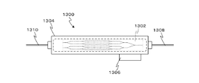
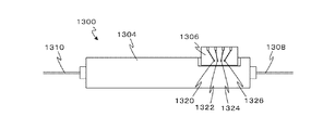
- FIG. 13A, FIG. 13B, and FIG. 13C are diagrams showing the configuration of a conventional optical modulator having such an FPC.
- FIG. 13A is a top view of the optical modulator
- FIG. 13B is a front view
- FIG. It is.
- This optical modulator 1300 includes an optical modulation element 1302, a housing 1304 that accommodates the optical modulation element 1302, a flexible printed circuit board (FPC) 1306, an optical fiber 1308 for making light incident on the optical modulation element 1302, an optical An optical fiber 1310 that guides the light output from the modulation element 1302 to the outside of the housing 1304.
- FPC flexible printed circuit board
- the housing 1304 is provided with four lead pins 1320, 1322, 1324, 1326 respectively connected to four RF electrodes (not shown) of the light modulation element 1302, and the lead pins 1320, 1322, 1324, 1326 are respectively
- the through holes 1420, 1422, 1424, and 1426, which will be described later, provided in the FPC 1306 are inserted and fixed, for example, by solder and electrically connected.
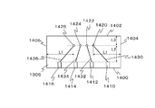
- FIG. 14 is a diagram illustrating a configuration of the FPC 1306.
- four pads 1410, 1412, 1414, and 1416 are arranged in the vicinity of one side 1400 on the lower side in the drawing along the direction of the one side 1400. Further, on the side of the other side 1402 facing the side 1400, for example, four through holes 1420, 1422, 1424, and 1426 are provided side by side along the direction of the side 1402. Further, the four pads 1410, 1412, 1414, 1416 are electrically connected to the through holes 1420, 1422, 1424, 1426 by wiring patterns 1430, 1432, 1434, 1436, respectively.
- the four pads 1410, 1412, 1414, and 1416 are fixed to and electrically connected to pads on the external circuit board, for example, by soldering, so that the RF of the light modulation element 1302 included in the light modulator 1300 is obtained.
- the electrode and the electronic circuit configured on the circuit board are electrically connected and mounted in the optical transmission device.
- the shape of the FPC 1306 is generally a horizontally long rectangle having a short side in the signal transmission direction as shown in the figure in order to shorten the wiring pattern as much as possible and keep the microwave loss low.
- the rectangular shape is about 20 mm or less in the long side direction and about 10 mm or less in the short side direction.
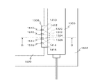
- FIG. 15A and 15B are diagrams illustrating an example of a state in which the optical modulator 1300 is connected to a circuit board on which an electronic circuit is configured.
- FIG. 15A is a diagram viewed from the top surface of the optical modulator 1300, and FIG. It is a BB cross-sectional arrow view in FIG. 15A.
- FIG. 15B the description of the internal configuration of the optical modulator 1300 is omitted.
- the optical modulator 1300 and the circuit board 1500 are fixed to, for example, a base 1502 in the housing of the optical transmission device.
- the FPC 1306 of the optical modulator 1300 extends to the left in the drawing from the connection portion with the lead pins 1320, 1322, 1324, and 1326, and the left end portion is on the circuit board 1500 as shown in FIG. 15B. It is bent in the diagonally lower left direction so as to be in contact with.
- the pads 1410, 1412, 1414, 1416 of the FPC 1306 are fixed and electrically connected to the pads 1510, 1512, 1514, 1516 on the circuit board 1500 by, for example, solder (FIG. 15A).
- the FPC 1306 has the through holes 1420, 1422, 1424, and 1426 fixed to the lead pins 1320, 1322, 1324, and 1326 of the optical modulator housing 1304 by, for example, soldering when the optical modulator 1300 is manufactured. Connected.
- the pads 1410, 1412, 1414, 1416 are fixed to the pads 1510, 1512, 1514, 1516 on the circuit board 1500 by, for example, solder and electrically connected. Is done. At this time, as can be understood from FIG.
- the FPC 1306 includes a through hole 1420 (that is, a solder fixing portion or a solder connection portion with the lead pin 1320) to a right side 1404 and a through hole 1426 (that is, the lead pin). 1326 (solder fixing portion or solder connecting portion) to the side 1406 on the left side of the figure together constitutes a cantilever of length L1 (referred to as first and second cantilever beams, respectively) It vibrates according to the vibration (environmental vibration) of the installation environment of the optical modulator 1300.
- a through hole 1420 that is, a solder fixing portion or a solder connection portion with the lead pin 1320
- 1326 solder fixing portion or solder connecting portion
- the portions from the through holes 1420, 1422, 1424, 1426 (that is, the fixing portions to the lead pins 1320, 1322, 1324, 1326) to the pads 1410, 1412, 1414, 1416 have both lengths L2.
- a portion from the through holes 1420, 1422, 1424, and 1426 to the upper side 1402 in the figure constitutes a cantilever having a length of L3 (referred to as a third cantilever).
- a cantilever having a length of L3 referred to as a third cantilever.
- each of them vibrates in response to environmental vibration (that is, in the rectangular FPC shown in FIG. 14, there are four vibrations: the vibration of the above-mentioned cantilever beam and the vibration of the above-mentioned first to third cantilever beams. Vibration mode exists).
- a heat dissipation fan provided in the optical transmission device, a device rack (rack) in which the optical transmission device is accommodated
- a cooling fan air-conditioning vibration of a room where the light modulation device is installed
- various vibrations transmitted to the building where the light modulation device is installed may be many factors such as a cooling fan, air-conditioning vibration of a room where the light modulation device is installed, and various vibrations transmitted to the building where the light modulation device is installed.
- the cantilever part and / or the cantilever part when the frequency of these environmental vibrations is close to the natural vibration frequency determined by the substrate rigidity of the FPC 1306 and the lengths L1, L2, L3, etc., the cantilever part and / or the cantilever part is Then, it may vibrate with a large amplitude like a resonance vibration. As a result, peeling or cracking may occur in the solder fixing portion or the solder connecting portion between the through holes 1420, 1422, 1424, 1426 and the lead pins 1320, 1322, 1324, 1326 that function as fixed ends of these beam portions.
- the natural frequency of the beam portion becomes lower as the corresponding lengths L1, L2, and L3 are longer, and the power spectral density in the environmental vibration falls within a large frequency range, so that the influence of the environmental vibration is reduced. It becomes easy to receive.
- the portion having the length L1 or L2 is more easily affected by the environmental vibration than the portion having the length L3. More specifically, for example, the portion of the length L1 in FIG. 14 vibrates as shown by a thick arrow in FIG. 16A, and in particular, peeling or cracking occurs in the solder fixing portions or solder connection portions of the lead pins 1320 and 1326, 14 may vibrate as indicated by a thick arrow in FIG. 16B to cause peeling or cracking in the solder fixing portions or solder connection portions of the lead pins 1320, 1322, 1324, and 1326.
- the inner diameters of the through holes 1420, 1422, 1424, and 1426 are such that the frequency of a high-frequency signal to be applied to the light modulation element 1302 may reach several tens of GHz, so that the lead pins 1320, 1322, Similar to the diameters of 1324 and 1326, the diameter is as small as several hundred ⁇ m, and is more susceptible to the environmental vibration than ordinary electronic devices that handle lead pins of around 1 mm.
- One aspect of the present invention is an optical modulator including a flexible wiring board that performs electrical connection with a circuit board.
- the flexible wiring board has a substantially quadrangular shape, and the flexible wiring board is provided with a pad that is electrically connected to the circuit board along one side of the substantially quadrilateral.
- a signal pattern connected to a signal lead pin for signal transmission provided in the optical modulator is provided on the other side opposite to the one side.
- the flexible wiring board has an additional fixing part and / or a notch for increasing the frequency of the natural vibration of the flexible wiring board in a state of being connected to the signal lead pins and the circuit board.
- the additional fixing portion includes an additional pattern connected to an additional lead pin provided in addition to the optical modulator in addition to the signal lead pin.
- the additional pattern is configured to electrically connect a ground pattern provided on a flexible wiring board and the housing of the optical modulator.
- the additional fixing portion includes two sides excluding the one side and the other side of the substantially quadrangular shape, and both ends of the signal pattern arrangement portion. The additional pattern is provided with at least one each between them.
- the additional fixing portion includes at least one additional pattern provided between the array portion and the one side.
- the additional fixing portion is further configured by at least one additional pattern provided between the array portion and the other side.
- the additional pattern provided between the array portion and the one side, and the additional pattern provided between the array portion and the other side A distance d measured in a direction perpendicular to the one side, the additional pattern provided between the end of the pad facing the one side, the array portion and the one side And a distance Lp measured in a direction perpendicular to the one side, d ⁇ Lp / 5.
- the additional pattern provided between the array portion and the one side, and the additional pattern provided between the array portion and the other side, Each of the signal patterns is arranged so as to surround from four sides.
- the additional fixing portion further includes at least one each between two sides excluding the one side and the other side and both ends of the array portion.
- the additional pattern is provided.
- a notch is provided from each of the two sides excluding the one side and the other side toward the array portion.
- the two sides excluding the one side and the other side opposite to the one side, and the two corners formed by the other side, respectively, have notches.
- the notch is a distance from both ends of the array portion to the edge of the notch, and the distance along the direction of the one side is the distance from the one side to the one side. It changes so that it may change according to the distance measured along the direction orthogonal to the edge
- the array part is composed of one or more array parts, and each of two array parts closest to each of two sides excluding the one side and the other side. The distance between the end and the corresponding side of the two sides is different from each other.
- Another aspect of the present invention is an optical transmission device including any one of the optical modulators described above and an electronic circuit that outputs an electrical signal for causing the optical modulator to perform a modulation operation.
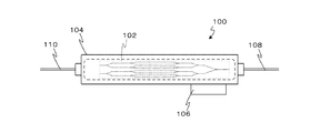
- FIG. 1 is a top view of an optical modulator according to a first embodiment of the present invention.
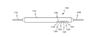
- 1 is a side view of an optical modulator according to a first embodiment of the present invention.
- 1 is a bottom view of an optical modulator according to a first embodiment of the present invention.
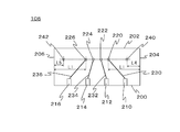
- It is a figure which shows the structure of FPC used for the optical modulator shown to FIG. 1A.
- It is a figure which shows an example of the state which connected the optical modulator shown to FIG. 1A to the circuit board in which the electronic circuit was comprised.
- It is a figure which shows an example of the state which connected the optical modulator shown to FIG. 1A to the circuit board in which the electronic circuit was comprised.
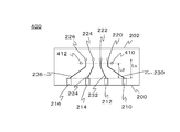
- It is a figure which shows the 1st modification of FPC used for the optical modulator shown to FIG.
- FIG. 1A It is a figure which shows the structure of the optical transmission apparatus which concerns on the 2nd Embodiment of this invention. It is a top view of the conventional optical modulator. It is a side view of the conventional optical modulator. It is a bottom view of the conventional optical modulator. It is a figure which shows the structure of FPC used for the optical modulator shown to FIG. 13A. It is a figure which shows an example of the state which connected the optical modulator shown to FIG. 13A to the circuit board in which the electronic circuit was comprised. It is a figure which shows an example of the state which connected the optical modulator shown to FIG. 13A to the circuit board in which the electronic circuit was comprised. It is a figure which shows an example of the vibration aspect of FPC used for the optical modulator shown to FIG. 13A. It is a figure which shows an example of the vibration aspect of FPC used for the optical modulator shown to FIG. 13A.
- the optical modulator of the present embodiment includes a substantially quadrangular flexible wiring board that performs electrical connection with a circuit board, and the flexible wiring board is attached to a signal lead pin provided in the housing of the optical modulator. It is connected.
- the flexible wiring board has an additional fixing portion for increasing the natural vibration frequency of the vibration with the connecting portion between the flexible wiring board and the signal lead pin and the circuit board as a fixing end.
- the additional fixing portion is configured by an additional wiring pattern connected to an additional lead pin provided in addition to the housing of the optical modulator.
- the optical modulator 100 includes an optical modulation element 102, a housing 104 that houses the optical modulation element 102, a flexible wiring board (FPC) 106, an optical fiber 108 for making light incident on the optical modulation element 102, And an optical fiber 110 that guides light output from the modulation element 102 to the outside of the housing 104.
- FPC flexible wiring board
- the light modulation element 102 includes, for example, four Mach-Zehnder type optical waveguides provided on an LN substrate, and four high-frequency electrodes (RF electrodes) that are provided on the Mach-Zehnder type optical waveguide and modulate light waves propagating in the optical waveguide. And a DP-QPSK optical modulator.
- the two lights output from the light modulation element 102 are polarized and combined by a lens optical system, for example, and guided to the outside of the housing 104 via the optical fiber 110.
- the housing 104 includes four signal lead pins 120, 122, 124, 126 connected to four RF electrodes (not shown) included in the light modulation element 102.
- Signal lead pins 120, 122, 124, 126 provided on the housing 104 are inserted into signal through holes 220, 222, 224, 226 described later provided on the FPC 106, and the signal through holes 220, 222, 224 are inserted. 226 and the signal lead pins 120, 122, 124, 126 are connected and fixed by, for example, solder.
- FIG. 2 is a diagram showing the configuration of the FPC 106.
- the FPC 106 is manufactured using, for example, a substrate made of polyimide as a main material (hereinafter referred to as an FPC substrate).
- the FPC 106 is configured to be rectangular in plan view.
- the shape of the FPC 1306 is generally a horizontally long rectangle in order to shorten the wiring pattern as much as possible to keep the microwave loss low.
- the FPC 106 has a rectangular shape, like the FPC 1306.
- the shape of the FPC 106 is not limited to this, and may be a substantially quadrangular shape, for example.
- side refers to a rectangular side formed by the FPC 106, but when the FPC 106 is configured by a substantially quadrilateral, the “side” refers to the side of the substantially quadrilateral formed by the FPC 106. Means.
- four pads 210, 212, 214, and 216 are provided side by side along the direction of the one side 200. Further, on the side of the other side 202 facing the side 200, for example, four signal through holes 220, 222, 224, and 226 are provided side by side along the direction of the side 202. Further, the four pads 210, 212, 214, and 216 are electrically connected to the signal through holes 220, 222, 224, and 226 by wiring patterns 230, 232, 234, and 236, respectively.
- the four signal through holes 220, 222, 224, and 226 are connected to the four signal lead pins 120, 122, 124, and 126 included in the housing 104, respectively. Therefore, the pads 210, 212, 214, and 216 are electrically connected (for example, by soldering) to the pads that constitute a part of the electronic circuit provided on the external circuit board, respectively.
- the output high frequency signal is applied to the RF electrode of the light modulation element 102 via the FPC 106. That is, the signal through holes 220, 222, 224, and 226 are signal patterns that are connected to the signal lead pins 120, 122, 124, and 126 for signal transmission provided in the optical modulator 100.
- the wiring patterns 230, 232, 234, and 236 provided in the FPC 106 may be configured using a known line configuration as a high-frequency signal line such as a microstrip line, a coplanar line, or a grand coplanar line.
- a ground pattern may be provided on the FPC 106 (not shown).
- the size of the FPC 106 is, for example, the length in the long side direction (direction of the side 200) in order to shorten the wiring patterns 230, 232, 234, and 236 as much as possible to reduce the microwave loss.
- the length in the short side direction (direction perpendicular to the side 200) can be about 10 mm or less.
- FIG. 3A and 3B are diagrams illustrating an example of a state in which the optical modulator 100 is connected to a circuit board on which an electronic circuit is configured.
- FIG. 3A is a diagram viewed from the top surface of the optical modulator 100, and FIG. It is AA cross-sectional arrow view in FIG. 3A.
- FIG. 3B the description of the internal configuration of the optical modulator 100 is omitted.
- the optical modulator 100 and the circuit board 300 are fixed to the base 302 in the housing of the optical transmission device, for example.
- the FPC 106 of the optical modulator 100 extends to the left in the drawing from the connection portion with the signal lead pins 120, 122, 124, 126, and as shown in FIG.
- the board is bent in the diagonally lower left direction so as to be in contact with the substrate 300, whereby the pads 210, 212, 214, 216 of the FPC 106 are fixed to the pads 310, 312, 314, 316 on the circuit board 300 by, for example, soldering and electrical (FIG. 3A).
- one side 200 provided with the pads 210, 212, 214, and 216 and signal through holes 220, 222, 224, and 226 are provided.
- additional through holes 240 and 242 which are additional patterns are provided between the respective end portions close to the two sides 204 and 206 (that is, portions of the signal through holes 220 and 226).
- the distance L1 is between the signal through hole 220 and the side 204 and between the signal through hole 226 and the side 206, and is between the signal through hole 220 and the side 204.
- the additional through hole 240 is provided at a position at a distance L4 ( ⁇ L1) from the side 204, and the additional through hole is provided at a position at a distance L5 ( ⁇ L1) from the side 206 between the signal through hole 226 and the side 206.
- a hole 242 is provided.
- the additional through holes 240 and 242 as additional patterns are added to the signal lead pins 120, 122, 124, and 126 and added to the additional lead pins 132 and 130 provided on the housing 104 of the optical modulator 100, for example, by soldering. Fixed and electrically connected.
- the fixed ends of the two cantilever portions having the two sides 204 and 206 as free ends respectively become the additional through holes 240 and 242 instead of the signal through holes 220 and 226, respectively. Since the length of the arm of each cantilever portion is L4 and L5 shorter than L1, the natural circumferential frequency of the beam portion is higher than that in the case where the additional through holes 240 and 242 are not provided.
- the natural vibration frequency of the two cantilever portions each having the sides 204 and 206 as free ends is away from the frequency range of the environmental vibration, and the vibration of the sides 204 and 206 due to the environmental vibration is suppressed. Therefore, the peeling of the solder fixing portion or the solder connecting portion or the occurrence of cracks due to the environmental vibration is suppressed.
- the number of additional through holes provided between the signal through hole 220 and the side 204 and / or between the signal through hole 226 and the side 206 may be plural.
- the optical modulator 100 having the above configuration includes a flexible wiring board (FPC) 106 that performs electrical connection between the optical modulator 100 and a circuit board, and the signal through holes 220 and 222 of the FPC 106.
- FPC flexible wiring board
- 224, 226 and signal lead pins 120, 122, 124, 126 of the optical modulator 100 are connected to each other, and in addition to signal fixing holes, signal through holes 220, 222, 224 which are signal patterns.
- 226 between the signal through holes 220 and 226 which are the end portions of the arrangement portion 226 and the sides 204 and 206 on the side close to the signal through holes 220 and 226, respectively.
- Holes 240 and 242 are provided.
- the additional through holes 240 and 242 are connected to the additional lead pins 132 and 130 provided in the optical modulator 100, whereby an additional fixing portion is provided in the FPC 106.
- the present optical modulator 100 by adjusting the distances L4 and L5 from the sides 204 and 206 to the additional through holes 240 and 242, the natural vibration of the cantilever vibration having the sides 204 and 206 as free ends, respectively. Is shifted to a higher side away from the environmental vibration frequency range, and the vibration of the FPC 106 caused by the environmental vibration is suppressed to suppress the peeling of the solder fixing portion or the solder connection portion or the generation of cracks. it can.
- the additional fixing portion fixes the additional through holes 240 and 242 provided in the FPC 106 and the additional lead pins 132 and 130 provided in the optical modulator 100 by solder (which may be a conductive material other than solder).
- solder which may be a conductive material other than solder.
- the signal lead pins 120, 122, 124, 126 and the signal through holes 220, 222, 224, 226 can be formed at the same time. For this reason, it is possible to reduce the number of manufacturing steps of the additional fixing portion, and if the additional fixing portion is first solder-fixed, the signal lead pins 120, 122, 124, 126 and the signal through holes 220, 222 are provided. Since the mutual positional relationship between 224 and 226 is fixed, the operation of fixing the solder between them becomes easy, and the finished quality of the solder fixing portion is improved.
- the design (size, shape, etc.) of the additional lead pins 130, 132 and the additional through holes 240, 242 is the same as the design of the signal lead pins 120, 122, 124, 126 and the signal through holes 220, 222, 224, 226. Therefore, it is possible to unify the amount of solder, heating conditions, etc. between each lead pin and each through hole at the time of manufacturing, which is convenient from the viewpoint of manufacturing line work.
- the lengths L4 and L5 are different lengths, the natural vibration frequencies of the cantilever vibrations having the sides 204 and 206 as free ends are different from each other. Even if it spreads to the frequency of vibration, it can suppress that the part of edge
- the housing 104 of the optical modulator 100 is provided with an additional lead pin connected and fixed to an additional through hole provided in the FPC according to the modification.
- illustration of the modified example of the housing 104 having the additional lead pins corresponding to each modified example is omitted.
- both supported beam the portion between the signal through holes 220, 222, 224, 226 and the pads 210, 212, 214, 216 is referred to as “both supported beam” or “both supported beam portions”.
- the cantilever portion having the side 204 or its deformation (notch portion edge or the like) as a free end is also referred to as a “first cantilever portion” or a “first cantilever portion”.
- the vibration of the cantilever portion is also referred to as “first cantilever vibration”.
- a cantilever portion having the side 206 or its deformation (notch portion edge or the like) as a free end is also referred to as a “second cantilever portion” or a “second cantilever portion”.
- the vibration of the cantilever portion is also referred to as “second cantilever vibration”.
- the cantilever part having the side 202 as a free end is also referred to as “third cantilever part” or “third cantilever part”, and the vibration of the third cantilever part is referred to as “third cantilever part”. Also called “cantilever vibration”.
- an additional fixing portion is provided by the additional lead pins 130 and 132 and the additional through holes 240 and 242 to increase the natural vibration frequency of the cantilever vibration with the sides 204 and 206 as free ends. The vibration of the FPC 106 caused by the vibration is suppressed.
- connection portion between the signal through holes 220, 222, 224, 226 and the signal lead pins 120, 122, 124, 126 is one fixed end, and the pads 210, 212, 214, 216 are connected.
- the connection portion between the circuit board and the circuit board is used as the other fixed end, and the frequency of natural vibration of the both-end supported beam portion formed between these fixed ends is increased.
- FIG. 4 is a diagram showing a configuration of an FPC 400 that can be used in place of the FPC 106 according to this modification. 4, the same reference numerals as those in FIG. 2 are used for the same components as those of the FPC 106 illustrated in FIG. 2, and the above description of FIG. 2 is incorporated.
- the FPC 400 shown in FIG. 4 has the same configuration as the FPC 106 shown in FIG. 2, but does not have the additional through holes 240 and 242 and the signal through holes 220 to which the signal lead pins 120, 122, 124, and 126 are connected. , 222, 224, 226 and additional through holes 410, 412 between the pads 210, 212, 214, 216 provided on one side 200 and the ends of the pads facing the side 200. Is provided.
- the additional through-holes 410 and 412 are fixed to additional lead pins provided in the housing 104 of the optical modulator 100 to form an additional fixing portion (note that, in the following, avoiding redundant description and understanding)
- additional through hole means that the corresponding “additional lead pin” is connected to form an additional fixing portion).
- the distance Lp from the end of the pads 210, 212, 214, and 216 provided on the side 200 on the side facing the side 200 to the additional through holes 410 and 412 constituting the additional fixing portion is The distance Ls from the end to the signal through holes 220, 222, 224, and 226 is shorter than the distance Ls. That is, since the distance between the two fixed ends constituting the both-end supported beam portion of the FPC 400 is Lp shorter than Ls, the natural vibration frequency of the both-end supported beam portion is higher than the frequency range of environmental vibration.
- production of peeling and a crack of a solder connection part can be suppressed.
- the number of additional through holes provided between the arrangement portion of the signal through holes 220, 222, 224, and 226 and the pads 210, 212, 214, and 216 is the number of the additional through holes 410 and 412 as in the present embodiment.
- the number is not limited to two and can be any number of at least one or more.
- the distances between the additional through holes and the ends of the pads 210, 212, 214, and 216 facing the side 200 are made different from each other. , 212, 214, and 216 as two fixed ends, the frequency of the natural vibration of the doubly supported beam portion configured in the FPC 400 can be dispersed along the direction of the side 200. As a result, even if the environmental frequency coincides with the frequency of one natural vibration, it is avoided that the entire doubly supported beam portion having the width in the direction of the side 200 vibrates uniformly and greatly. The tolerance of the optical modulator 100 with respect to can be further increased.
- another side 202 (that is, a signal) facing one side 200 provided with pads 210, 212, 214, and 216 is provided.
- At least one additional through hole is also provided between the portion and the other side 202.
- FIG. 5 is a diagram showing a configuration of an FPC 500 that can be used in place of the FPC 106 according to this modification. 5, the same reference numerals as those in FIGS. 2 and 4 are used for the same components as those of the FPC 106 shown in FIG. 2 and the FPC 400 shown in FIG. 4. Incorporate.
- the FPC 500 shown in FIG. 5 has the same configuration as the FPC 400 shown in FIG. 4, but is further arranged with signal through holes 220, 222, 224, 226 to which the signal lead pins 120, 122, 124, 126 are connected. And additional side through holes 510 and 512 are provided between the side 202 facing the side 200 provided with the pads 210, 212, 214, and 216, and the additional through holes 510 and 512 are optically modulated. By fixing to an additional lead pin provided on the housing 104 of the container 100, an additional fixing portion is configured.
- the FPC 500 portion (both-supported beam portion) inherent between the pads 210, 212, 214, 216 and the signal through holes 220, 222, 224, 226 by the additional through holes 410, 412 is the same as the FPC 400.
- the additional through-holes 510 and 512 can also increase the frequency of natural vibration of the cantilever (third cantilever) portion having the side 202 as a free end.
- the additional through holes 410 and 510 are arranged on the side 204 side from the signal through hole 220 located at the right end in the figure of the arrangement portion of the signal through holes 220, 222, 224 and 226. ing.
- the additional through holes 412 and 512 are located closer to the side 206 than the signal through hole 226 located at the left end of the arrangement portion. For this reason, in this modified example, the frequency of the natural vibrations of the first and second cantilever portions having the sides 204 and 206 as free ends, respectively, is increased as in the FPC 106 shown in FIG. That is, the FPC 500 shown in FIG. 5 has four additional through-holes 410, 412, 510, and 512 that allow the four vibration modes (the vibration of the cantilever beam and the vibrations of the first to third cantilever beams). It is an efficient and effective configuration that can increase the frequency of all natural vibrations.
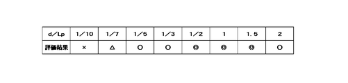
- the distance d measured along the direction orthogonal to the side 200 where the pads 210, 212, 214, and 216 are provided between the additional through holes 410 and 412 and the additional through holes 510 and 512 is narrow. If it is too large, the additional through holes 410, 412, 510, 512 will be too close to the signal through holes 220, 222, 224, 226, and the solder fixing portions or solder of the signal through holes 220, 222, 224, 226 The effect of defense against stress caused by the vibration of the FPC 500 with respect to the connection portion may be diminished.
- the distance d may have an optimum range in relation to the distance Lp between the additional through holes 410 and 412 and the pads 210, 212, 214, and 216.
- FIG. 6 shows the degree of peeling and / or cracking of the solder fixing portions or solder connecting portions of the signal lead pins 120, 122, 124, 126 after vibration and impact at various distances d normalized by the distance Lp. It is the result of evaluation.
- the evaluation shown in FIG. 6 ( ⁇ : very good, ⁇ : good, ⁇ : not enough, ⁇ : bad) was established by the Japan Welding Church “Quality criteria for micro soldering technology certification / certification test” ( Based on JWES-MS060801J), it is determined taking into account the uniformity of the finish.
- This quality judgment standard is based on the quality standard of highly reliable equipment described in JIS C 61191 “Printed wiring board mounting”. In part, the quality judgment standard is specified more specifically than the JIS requirement standard. ing.
- the additional through-holes 410, 412, 510, and 512 are set so that at least d ⁇ Lp / 5. It can be seen that it is preferable to arrange them, and in particular, it is more desirable that the range is 1/2 ⁇ d / Lp ⁇ 1.5.
- the additional through holes 510 and 512 and the additional through holes 410 and 412 are drawn at positions that are vertically symmetrical with respect to the signal through holes 220, 222, 224, and 226.
- the present invention is not limited to this, and the signal through holes 220, 222, 224, and 226 may be disposed asymmetrically.
- the FPC 500 is disposed at a symmetrical position as shown in FIG.
- This modified example has the same configuration as the second modified example shown in FIG. 5, but is provided with an arrangement portion of signal through holes 220, 222, 224, 226 and pads 210, 212, 214, 216.
- the plurality of additional through holes provided between the side 200 and the additional through hole provided between the arrangement portion and the side 202 facing the side 200 include signal through holes 220 and 222.
- Each of 224, 226 is arranged so as to surround each side.
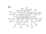
- FIG. 7 is a diagram showing a configuration of an FPC 700 that can be used in place of the FPC 106 according to this modification.
- the same reference numerals as those in FIG. 2 are used for the same components as those of the FPC 106 shown in FIG. 2, and the above description of FIG.
- the FPC 700 shown in FIG. 7 has the same configuration as the FPC 106 shown in FIG. 2, but does not have the additional through holes 240 and 242, and the signal through holes 220 to which the signal lead pins 120, 122, 124 and 126 are connected. , 222, 224, 226 and additional side holes 710, 712, 714, 716, 718 are provided between one side 200 where the pads 210, 212, 214, 216 are provided.
- additional through holes 720, 722, 724, 726, and 728 are provided between the arrangement portion and the side 202 facing the side 200. These additional through holes 710, 712, 714, 716, 718, 720, 722, 724, 726, 728 are arranged so as to surround each of the signal through holes 220, 222, 224, 226 from four sides. Yes.
- the signal through hole 220 is surrounded from four sides by the additional through holes 710, 712, 720, and 722, and the signal through hole 222 is surrounded from the four sides by the additional through holes 712, 714, 722, and 724 and is used for the signal.
- the through hole 224 is surrounded from four sides by additional through holes 714, 716, 724, and 726, and the signal through hole 226 is surrounded from four sides by additional through holes 716, 718, 726, and 728.
- the additional through holes 710, 712, 714, 716, 718, 720, 722, 724, 726, 728 are arranged at positions that surround the signal through holes 220, 222, 224, 226 from four sides. ing. Therefore, in this modification, the solder fixing portion or the solder connection portion in each of the signal through holes 220, 222, 224, and 226 is protected from vibration in all directions in the peripheral portion of the signal through hole, These additional through holes 710, 712, 714, 716, 718, 720, 722, 724, 726, and 728 make the four vibration modes in the FPC 700 (that is, both pads 210, 212, 214, and 216 have one fixed end). The frequency of all natural vibrations of the cantilever vibration and the first to third cantilever vibrations having the sides 202, 204, and 206 as free ends can be increased to reduce the influence of environmental vibration.
- the additional through holes 710, 712, 714, 716, 718, 720, 722, 724, 726, 728 are arranged symmetrically around the signal through holes 220, 222, 224, 226, respectively. It becomes easy to attach the FPC 700 to the housing 104 of the optical modulator 100 stably. Therefore, the signal through holes 220, 222, 224, and 226 at the solder fixing portion or the solder connection portion between the signal lead pins 120, 122, 124, and 126 and the signal through holes 220, 222, 224, and 226 are provided. There will be no variability in each.
- the electrical lines including the signal through holes 220, 222, 224, 226 (therefore, the signal lead pins 120, 122, 124, 126, the signal through holes 220, 222, 224, 226, the wiring pattern 230, 232, 234, and 236 and pads 210, 212, 214, and 216), and the high-frequency characteristics of each of the electrical lines) can be easily made smaller and equivalent. Become.
- FIG. 8 is a diagram showing a configuration of an FPC 800 that can be used in place of the FPC 106 according to this modification.
- the same reference numerals as those in FIGS. 2 and 7 are used for the same components as those of the FPC 106 and FPC 700 shown in FIGS. 2 and 7, and the description of FIGS. 2 and 7 is used. To do.
- the FPC 800 illustrated in FIG. 8 has the same configuration as the FPC 106 illustrated in FIG. 7, but further includes one side 200 provided with the pads 210, 212, 214, and 216 and the other side facing the one side 200. Cutout portions 810 and 812 are provided from the two sides 204 and 206 excluding 202 toward the arrangement portion of the signal through holes 220, 222, 224 and 226.
- notches are provided in the sides 204 and 206, so the additional through holes 710 and 720 are illustrated as fixed ends.
- the frequency of the natural vibration of the first cantilever vibration provided on the right side and the frequency of the natural vibration of the second cantilever vibration provided on the left side of the figure with the additional through holes 718 and 728 as fixed ends are shown in FIG. A significant shift to a higher frequency compared to the FPC 700 shown. For this reason, peeling of the solder fixing portion or the solder connecting portion in the signal through holes 220 and 226 due to the vibration of the first and second cantilever portions and generation of cracks are greatly suppressed.
- the depths of the cutout portions 810 and 812 are different from each other, and the distance L6 between the additional through holes 718 and 728 and the end portion of the cutout portion 812 provided from the side 206 is set.
- the distance L7 between the additional through holes 710 and 720 and the end of the notch 810 provided from the side 204 is short.
- the frequency of the natural vibration of the first cantilever beam having the additional through holes 710 and 720 as the fixed ends and the natural vibration of the second cantilever vibration having the additional through holes 718 and 728 as the fixed ends are obtained.
- the frequency is different.
- the first and second cantilever vibrations are prevented from occurring simultaneously with a large amplitude for the same environmental frequency. Since it can do, the tolerance of the optical modulator 100 with respect to environmental vibration can be improved more.
- cutout portions 810 and 812 may be provided so as to extend to the side 202 and to cut the corners of the sides 202 and 204 and the corners of the sides 202 and 206 into rectangles.
- FIG. 9 is a diagram illustrating a configuration of an FPC 900 that can be used in place of the FPC 106 according to the present modification. 9, the same reference numerals as those in FIGS. 2 and 7 are used for the same components as those of the FPC 106 and the FPC 700 shown in FIGS. 2 and 7, and the description of FIGS. 2 and 7 is used. To do.
- the FPC 900 shown in FIG. 9 has the same configuration as the FPC 700 shown in FIG. 7, but further includes one side 200 provided with signal through holes 220, 222, 224, 226 and pads 210, 212, 214, 216.
- Two through holes 710, 712, 716, 718 located between both ends of the array of the additional through holes 710, 712, 714, 716, and 718, and one side 200 and two sides excluding the side 202 opposite thereto.
- Additional through holes 910 and 912 are provided between the sides 204 and 206, respectively.
- the additional through holes 710 located at both ends of the arrangement of the additional through holes 710, 712, 714, 716, and 718 and Additional through-holes 910 and 912 are provided between 718 and sides 204 and 206, respectively.
- the natural frequency of the first and second cantilever vibrations having the sides 204 and 206 as free ends is shifted to a higher frequency than the configuration of FIG. For this reason, the peeling of the solder fixing portion or the solder connecting portion or the generation of cracks in the signal through holes 220 and 226 due to the cantilever vibration is greatly suppressed.
- the distance L6 between the side 204 and the additional through hole 910 and the distance L7 between the side 206 and the additional through hole 912 are different from each other.
- the frequency of the natural vibration of the cantilever vibration is different from the frequency of the natural vibration of the second cantilever vibration having the side 206 as a free end. For this reason, in this modification, even if the frequency range of the environmental vibration extends to these natural vibration frequencies, the first and second cantilever vibrations simultaneously with a large amplitude with respect to the same environmental frequency. Since generation
- the FPC 800 shown in FIG. 8 is used when it is difficult to provide a large notch in the FPC due to, for example, restrictions on the arrangement of electric lines in the FPC, restrictions on the FPC attachment jig, and the like. Can be used instead.
- a notch portion similar to the notch portions 810 and 812 shown in FIG. 8 is also provided, and the frequency of the natural vibration of the cantilever vibration is further increased to provide an optical modulator for environmental vibration.
- the resistance of 100 can be further increased.
- FIG. 10 is a diagram showing a configuration of an FPC 1000 that can be used in place of the FPC 106 according to this modification. 10, the same reference numerals as those in FIGS. 2 and 7 are used for the same components as those of the FPC 106 and the FPC 700 shown in FIGS. 2 and 7, and the description of FIGS. 2 and 7 is used. To do.
- the FPC 1000 shown in FIG. 10 has the same configuration as the FPC 700 shown in FIG. 7, but two sides except for one side 200 provided with pads 210, 212, 214, and 216 and the other side 202 facing the side. Notches 1020 and 1021 are provided at two corners 1010 and 1012 formed by 204 and 206 and the other side 202, respectively.
- the notches 1020 and 1021 are added through holes 710, 720, and 718 located at both ends of the arrangement portion of the additional through holes 710, 712, 714, 716, 718, 720, 722, 724, 726, and 728,
- the distance measured along the direction of the side 200 from the 728 to the respective edges 1030 and 1032 of the notches 1020 and 1021 is provided so as to change according to the distance from the one side 200.
- the notch 1020 is configured such that the distance from the additional through-holes 710 and 720 measured along the direction of the side 200 to the edge 1030 decreases as the distance from the side 200 increases.
- the distance L9 at the position of the additional through hole 720 that is distant from the additional through hole 710 with respect to the side 200 is shorter than the distance L8 at the provided position.
- a notch 1020 is provided so that the distance from the additional through-holes 710, 720 measured along the direction of the side 200 to the edge 1030 of the notch 1020 varies according to the distance from the side 200. Therefore, the frequency of the natural vibration of the first cantilever beam provided on the right side of the figure with the additional through holes 710 and 720 as fixed ends changes according to the distance from the side 200. For this reason, the frequency of the natural vibration of the first cantilever vibration with the edge 1030 as a free end is distributed in a finite frequency range, and the vibration amplitude of the cantilever vibration generated due to the environmental vibration. Is greatly suppressed.
- the frequency of the natural vibration of the second cantilever vibration having the edge 1032 as a free end is also distributed in a finite frequency range, and the cantilever generated due to environmental vibration.
- the vibration amplitude of vibration is also greatly suppressed.
- FIG. 11 is a diagram showing a configuration of an FPC 1100 that can be used in place of the FPC 106 according to this modification. 11, the same reference numerals as those in FIGS. 2 and 7 are used for the same components as those of the FPC 106 and the FPC 700 shown in FIGS. 2 and 7, and the description of FIGS. 2 and 7 is used. To do.
- the FPC 1100 shown in FIG. 11 has the same configuration as the FPCs 106 and 700 shown in FIGS. 2 and 7, but the signal through-hole arrangement part is separated and consists of two arrangement parts. Specifically, instead of the signal through holes 224 and 226 that are symmetrical with the signal through holes 220 and 222 across the left and right center line of the FPC 106, the left of the figure is shown from the position of the signal through holes 224 and 226. Signal through holes 1110 and 1112 are provided at positions moved in the direction. Thereby, the arrangement part of the signal through hole is composed of two arrangement parts, an arrangement part where the signal through holes 220 and 222 are arranged and an arrangement part where the signal through holes 1110 and 1112 are arranged. The
- the additional through holes 716, 718, 726, 728 of the FPC 700 shown in FIG. 7 are provided instead of the additional through holes 716, 718, 726, 728 of the FPC 700 shown in FIG. 7, the additional through holes arranged at positions moved to the left in the drawing from the positions of the additional through holes 716, 718, 726, 728. 1122, 1124, 1132 and 1134 are provided. Further, additional through holes 1120 and 1130 are provided, and the additional through holes 1120, 1122, 1124, 1130, 1132, and 1134 are arranged at positions that surround the signal through holes 1110 and 1112 from four directions.
- signal lead pins are provided at positions corresponding to the signal through holes 220, 222, 1110, and 1112 in the housing of the optical modulator. There is a need.
- the signal through hole arrangement portion is composed of two arrangement portions, that is, the signal through holes 220 and 222 and the signal through holes 1110 and 1112. Further, as described above, the signal through holes 1110 and 1112 are provided at positions that move to the left in the drawing from symmetrical positions with respect to the signal through holes 220 and 222 with the right and left center line interposed therebetween.
- the frequency of the natural vibration of the second cantilever vibration having the side 206 as a free end, the frequency of the natural vibration of the first cantilever vibration having the side 204 as a free end, Will be different. Therefore, even if the frequency range of the environmental vibration extends to these natural vibration frequencies, the first and second cantilever vibrations can be prevented from occurring simultaneously with a large amplitude for the same environmental frequency. Therefore, the tolerance of the light modulator 100 against environmental vibration can be further increased.
- additional through holes 710, 712, 714, 720, 722, 724, 1120, 1122, 1124, 1130, and 1322 are provided at positions that surround the signal through holes 220, 222, 1110, and 1112 from four directions. 1134 are provided. Therefore, similar to the FPC 700 shown in FIG. 7, the solder fixing portion or the solder connecting portion in each of the signal through holes 220, 222, 1110, and 1112 is caused by vibrations in all directions in the peripheral portion of the signal through hole. It is protected.
- these additional through-holes 710, 712, 714, 720, 722, 724, 1120, 1122, 1124, 1130, 1132, and 1134 allow the four vibration modes in the FPC 1100 (the vibration of the both-end supported beam portion and the first
- the frequency of all natural vibrations (vibration of the third cantilever part) can be increased to reduce the influence of environmental vibrations.
- a ground pattern (not shown) provided in each FPC has additional through holes (240 etc.) and additional lead pins (132 etc.).
- the optical modulator 100 (or a modification thereof) can be connected to the housing ground. Thereby, the fluctuation
- the present embodiment is an optical transmission device on which the optical modulator 100 (including any modifications shown in FIGS. 4 to 11) shown in the first embodiment is mounted.
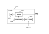
- FIG. 12 is a diagram showing a configuration of the optical transmission apparatus according to the present embodiment.
- the optical transmission apparatus 1200 includes an optical modulator 1202, a light source 1204 that makes light incident on the optical modulator 1202, a modulation signal generation unit 1206, and a modulation data generation unit 1208.
- the optical modulator 1202 is the optical modulator 100 illustrated in FIG. 1A (instead of the FPC 106, the optical modulator 1202 may include any of the FPCs 400, 500, 700, 900, or 1000 illustrated in FIGS. Alternatively, it may be a modification of the optical modulator including the FPC 1100 shown in FIG.
- the modulation data generation unit 1208 receives transmission data given from the outside, generates modulation data for transmitting the transmission data (for example, data obtained by converting or processing the transmission data into a predetermined data format), and The generated modulation data is output to modulation signal generation section 1206.
- the modulation signal generation unit 1206 is an electronic circuit that outputs an electric signal for causing the optical modulator 1202 to perform a modulation operation. Based on the modulation data output from the modulation data generation unit 1208, the modulation signal generation unit 1206 sends the modulation data to the optical modulator 1202.
- a modulation signal which is a high-frequency signal for performing an optical modulation operation according to the above, is generated and input to the optical modulator 100.
- the modulation signal includes four RF signals corresponding to four RF electrodes (not shown) of the light modulation element 102 included in the light modulator 100.
- the four RF signals are respectively input to pads 210, 212, 214, and 216 of the FPC 106 of the optical modulator 100 (which may be any of the above-described modifications of the FPC 106 as described above), and the wiring pattern 230, 232, 234, 236, signal through holes 220, 222, 224, 226, and signal lead pins 120, 122, 124, 126 are applied to the RF electrodes, respectively.
- the light output from the light source 1204 is modulated by the optical modulator 100 and is output from the optical transmission device 1200 as modulated light.
- the optical modulator 100 having the above-described configuration is used in the present optical transmission device 1200, the solder fixing portion or the solder connection portion in the FPC 106 caused by environmental vibration during transportation or operation of the optical transmission device 1200 can be reduced. The generation of cracks can be suppressed and good optical transmission quality can be ensured.
- an optical modulator including an optical modulation element having four RF electrodes using LN as a substrate is shown.
- the present invention is not limited to this, and a number of RFs other than four is provided.
- the present invention can be similarly applied to an optical modulator having an electrode and / or an optical modulator using a material other than LN as a substrate.
- the configuration of the FPC 106 shown in FIG. 2 and the configuration of the modified example of the FPC 106 shown in FIGS. 4 to 11 can not only be used individually as individual FPCs, but also can be combined into a single one by appropriately combining those configurations.
- An FPC may be configured and used.
Landscapes
- Physics & Mathematics (AREA)
- Nonlinear Science (AREA)
- Engineering & Computer Science (AREA)
- General Physics & Mathematics (AREA)
- Optics & Photonics (AREA)
- Microelectronics & Electronic Packaging (AREA)
- Electromagnetism (AREA)
- Chemical & Material Sciences (AREA)
- Ceramic Engineering (AREA)
- Crystallography & Structural Chemistry (AREA)
- Optical Modulation, Optical Deflection, Nonlinear Optics, Optical Demodulation, Optical Logic Elements (AREA)
- Structure Of Printed Boards (AREA)
Abstract
FPCを備えた光変調器において、搬送時や稼働時の振動に起因するハンダ固定部の剥離や割れを抑制して、信号経路の高周波特性の劣化を効果的且つ安価に抑制すること。 本発明に係る光変調器(100)は、回路基板との間の電気的接続を行うフレキシブル配線板(106)を備える。前記フレキシブル配線板は略四辺形を為し、前記フレキシブル配線板には、前記略四辺形の一の辺に沿って前記回路基板と電気的に接続されるパッド(210等)が設けられている。また、前記フレキシブル配線板には、前記一の辺に対向する他の辺に前記光変調器に設けられた信号伝達のための信号用リードピン(120等)と接続される信号用パターン(220等)が設けられている。さらに、前記フレキシブル配線板は、前記信号用リードピン及び前記回路基板に接続された状態における当該フレキシブル配線板の固有振動の周波数を高めるための、追加の固定部(240等)及び又は切り欠き部(810等)を有する。
Description
本発明は、光変調器及び光送信装置に関し、特に、高周波信号を入力するためのFPC(Flexible Printed Circuits、フレキシブル配線板)を備える光変調器、及びそれを用いた光送信装置に関する。
高速/大容量光ファイバ通信システムにおいては、導波路型の光変調素子を組み込んだ光変調器が多く用いられている。中でも、電気光学効果を有するLiNbO3(以下、LNともいう)を基板に用いた光変調素子は、光の損失が少なく且つ広帯域な光変調特性を実現し得ることから、高速/大容量光ファイバ通信システムに広く用いられている。
このLNを用いた光変調素子では、マッハツェンダ型光導波路と、当該光導波路に変調信号である高周波信号を印加するためのRF電極と、当該導波路における変調特性を良好に保つため種々の調整を行うためのバイアス電極と、が設けられている。そして、光変調素子に設けられたこれらの電極は、当該光変調素子を収容する光変調器の筺体に設けられたリードピンやコネクタを介して、外部の電子回路に接続される。
一方、光ファイバ通信システムにおける変調方式は、近年の伝送容量の増大化の流れを受け、QPSK(Quadrature Phase Shift Keying)やDP-QPSK(Dual Polarization - Quadrature Phase Shift Keying)等、多値変調や、多値変調に偏波多重を取り入れた伝送フォーマットが主流となっている。
QPSK変調を行う光変調器(QPSK光変調器)やDP-QPSK変調を行う光変調器(DP-QPSK光変調器)は、入れ子構造になった複数のマハツェンダ型光導波路を備え、複数の高周波信号電極及び複数のバイアス電極を備えることから(例えば、特許文献1参照)、光変調器の筺体のサイズが大型化する傾向があり、特に小型化の要請が強い。
この小型化の要請に対応する一つの策として、従来、RF電極のインタフェースとして光変調器の筺体に設けられていたプッシュオン型の同軸コネクタを、バイアス電極のインタフェースと同様のリードピンに置き換え、これらのリードピンを外部の回路基板に接続するためのFPC(フレキシブル配線板(FPC:Flexible Printed Circuits)を付加した光変調器が提案されている。
例えば、DP-QPSK光変調器では、それぞれにRF電極を有する4つのマッハツェンダ型光導波路で構成される光変調素子が用いられる。この場合、光変調器の筺体に4つのプッシュオン型同軸コネクタを設けたのでは筺体の大型化は避けられないが、同軸コネクタに代えてリードピンとFPCとを用いれば、小型化が可能となる。
また、光変調器の筺体のリードピンと、当該光変調器に変調動作を行わせるための電子回路が搭載された回路基板と、の間が、上記FPCを介して接続されるので、従来用いていた同軸ケーブルの余長処理を行う必要が無くなり、光送信装置内における光変調器の実装スペースを縮小することができる。
光変調器に用いられるFPCは、例えば柔軟性のあるポリイミドベースの材料を基板(以下、FPC基板)として用いて作製され、一方の端部付近に設けられた複数のスルーホールのそれぞれが、配線パターンを介して、他方の端部に設けられたパッドのそれぞれに電気的に接続されている。そして、光変調器の筺体の底面又は側面から突き出た複数のリードピンが上記複数のスルーホールにそれぞれ挿通されて例えばハンダにより固定され且つ電気的に接続され、上記複数のパッドが回路基板に例えばハンダにより固定され且つ接続される。これにより、当該回路基板上のパッドから与えられる高周波信号が、それぞれ対応する上記スルーホールとリードピンとを介して、光変調素子の対応するRF電極に与えられて、高速光変調が行われる。
上記のFPCを用いた光変調器では、上述のように、筺体を小型化することができ、回路基板上における光変調器の実装スペースも縮小することができるので、光伝送装置の小型化に大きく貢献し得る。
図13A、図13B、図13Cは、そのようなFPCを備える従来の光変調器の構成を示す図であり、図13Aは光変調器の上面図、図13Bは正面図、図13Cは底面図である。この光変調器1300は、光変調素子1302と、光変調素子1302を収容する筺体1304と、フレキシブル配線板(FPC)1306と、光変調素子1302に光を入射するための光ファイバ1308と、光変調素子1302から出力される光を筺体1304の外部へ導く光ファイバ1310と、を備える。
筺体1304には、光変調素子1302の4つのRF電極(不図示)にそれぞれ接続された4つのリードピン1320、1322、1324、1326が設けられており、当該リードピン1320、1322、1324、1326は、FPC1306に設けられた後述するスルーホール1420、1422、1424、1426に挿通されて例えばハンダにより固定され且つ電気的に接続されている。
図14は、FPC1306の構成を示す図である。FPC1306は、図示下側の一の辺1400の近傍に、当該一の辺1400の方向に沿って4つのパッド1410、1412、1414、1416が並んで設けられている。また、辺1400に対向する他の辺1402の側には、例えば辺1402の方向に沿って、4つのスルーホール1420、1422、1424、1426が並んで設けられている。さらに、4つのパッド1410、1412、1414、1416は、それぞれ、配線パターン1430、1432、1434、1436によりスルーホール1420、1422、1424、1426に電気的に接続されている。
そして、4つのパッド1410、1412、1414、1416が外部の回路基板のパッドに対してそれぞれ例えばハンダにより固定され且つ電気的に接続されることにより、光変調器1300が備える光変調素子1302のRF電極と当該回路基板上に構成された電子回路とが電気的に接続されて光送信装置内に実装される。なお、FPC1306の形状は、配線パターンを極力短くしてマイクロ波損失を低く抑えるべく、図示のように信号伝送方向に短い辺を持つ横長の長方形になるのが一般的であり、図示の例のように4つのパッド1410、1412、1414、1416を持つ場合には、長辺方向で約20mm以下、短辺方向で約10mm以下程度の長方形となる。
図15A、図15Bは、電子回路が構成された回路基板に光変調器1300を接続した状態の一例を示す図であり、図15Aは光変調器1300の上面方向から見た図、図15Bは図15AにおけるBB断面矢視図である。なお、図15Bにおいて光変調器1300の内部の構成については記載を省略している。
光変調器1300と回路基板1500とは、例えば光送信装置の筺体内のベース1502に固定されている。図15Aに示すように、光変調器1300のFPC1306は、リードピン1320、1322、1324、1326との接続部分から図示左方へ延在し、図15Bに示すように、左側端部が回路基板1500に接するように図示斜め左下方向に曲げられている。これにより、FPC1306のパッド1410、1412、1414、1416は、回路基板1500上のパッド1510、1512、1514、1516に、例えばハンダにより固定され且つ電気的に接続される(図15A)。
しかしながら、上記のようなFPC付き光変調器を光送信装置内の回路基板に接続し、当該光送信装置を搬送してその稼働を開始すると、当該搬送の途中や稼働時の設置環境における振動等により、光変調器の筺体1304のリードピン1320、1322、1324、1326とFPC1306のスルーホール1420、1422、1424、1426との間のハンダ固定部又はハンダ接続部に剥離やヒビ割れを生じ得る。その結果、FPC1306のパッド1410、1412、1414、1416からリードピン1320、1322、1324、1326に至るまでの高周波特性が劣化又は変化することとなって、光変調器1300における光変調特性に問題を生じ得る。
上述したように、FPC1306は、光変調器1300の製造の際にスルーホール1420、1422、1424、1426が光変調器の筺体1304のリードピン1320、1322、1324、1326に例えばハンダにより固定され且つ電気的に接続される。そして、光変調器1300を光送信装置内で用いる際には、パッド1410、1412、1414、1416が回路基板1500上のパッド1510、1512、1514、1516に例えばハンダにより固定され且つ電気的に接続される。このとき、FPC1306は、図14から理解され得るように、スルーホール1420(すなわち、リードピン1320とのハンダ固定部又はハンダ接続部)から図示右側の辺1404までの部分及びスルーホール1426(すなわち、リードピン1326とのハンダ固定部又はハンダ接続部)から図示左側の辺1406までの部分が、共に長さL1の片持ち梁(それぞれ、第1及び第2の片持ち梁という)を構成することとなり、光変調器1300の設置環境の振動(環境振動)に応じて振動することとなる。また、同様に、スルーホール1420、1422、1424、1426(すなわち、リードピン1320、1322、1324、1326との固定部)からパッド1410、1412、1414、1416までの部分が、長さL2の両持ち梁を構成することとなり、スルーホール1420、1422、1424、1426から図示上方の辺1402までの部分が、長さがL3の片持ち梁(第3の片持ち梁という)を構成することとなって、それぞれが環境振動に応じて振動することとなる(すなわち、図14に示す矩形のFPCでは、上記両持ち梁の振動、及び上記第1ないし第3の片持ち梁の振動の、4つの振動モードが存在する)。
環境振動としては、光変調器1300及び当該光変調器1300を用いる光送信装置の、搬送や組み付け時の振動のほか、光送信装置が備える放熱ファン、光送信装置が収容される装置架(ラック)の冷却ファン、光変調装置が設置される部屋の空調振動、光変調装置が設置される建物に伝達されるさまざまな振動など、多くの要因が存在し得る。
そして、特にこれらの環境振動の周波数が、FPC1306の基板剛性と上記長さL1、L2、L3等とで定まる固有振動の周波数に近い場合には、上記片持ち梁部分及び又は両持ち梁部分は、共振振動のように大きな振幅を伴って振動することとなり得る。その結果、これら梁部分の固定端として機能するスルーホール1420、1422、1424、1426とリードピン1320、1322、1324、1326とのハンダ固定部又はハンダ接続部に、剥離やひび割れが生じ得る。
ここで、上記梁部分の固有周波数は、対応する長さL1、L2,L3が長いほど低くなり、環境振動におけるパワースペクトル密度が大きい周波数範囲内に入ることとなって、当該環境振動の影響を受けやすくなる。例えば、図14のような構成のFPC1306の場合、環境振動の影響を受けやすいのは、長さL3の部分よりも長さL1又はL2の部分となる。より具体的には、例えば図14における長さL1の部分は、図16Aに太線矢印で示す如く振動して、特にリードピン1320及び1326のハンダ固定部又はハンダ接続部に剥離やひび割れを発生させ、図14における長さL2の部分は、図16Bに太線矢印で示す如く振動して、リードピン1320、1322、1324、1326のハンダ固定部又はハンダ接続部に剥離やひび割れを発生させ得る。
特に、スルーホール1420、1422、1424、1426の内径は、光変調素子1302に印加されることとなる高周波信号の周波数が数十GHz程度にまで及ぶ可能性があることから、リードピン1320、1322、1324、1326の直径と同様に数百μm程度と小さく、1mm前後のリードピンを扱う通常の電子機器に比べて上記環境振動の影響を受け易い。
上記背景より、外部の回路基板との電気的接続を行うFPCを備えた光変調器において、搬送時や稼働時の振動に起因する例えばハンダにより固定部又は電気的接続部の剥離や割れを抑制して、信号経路の高周波特性の劣化を効果的且つ安価に抑制することが望まれている。
本発明の一の態様は、回路基板との間の電気的接続を行うフレキシブル配線板を備えた光変調器である。当該光変調器では、前記フレキシブル配線板は略四辺形を為し、前記フレキシブル配線板には、前記略四辺形の一の辺に沿って前記回路基板と電気的に接続されるパッドが設けられ、且つ前記一の辺に対向する他の辺に前記光変調器に設けられた信号伝達のための信号用リードピンと接続される信号用パターンが設けられている。また、前記フレキシブル配線板は、前記信号用リードピン及び前記回路基板に接続された状態における当該フレキシブル配線板の固有振動の周波数を高めるための、追加の固定部及び又は切り欠き部を有する。
本発明の他の態様によると、前記追加の固定部は、前記信号用リードピンに加えて前記光変調器に追加して設けられた追加リードピンと接続される追加パターンで構成される。
本発明の他の態様によると、前記追加パターンは、フレキシブル配線板に設けられたグランドパターンと前記光変調器の筺体とを電気的に接続するよう構成されている。
本発明の他の態様によると、前記追加の固定部は、前記略四辺形の前記一の辺及び前記他の辺を除く二つの辺と、前記信号用パターンの配列部分の両端部と、の間にそれぞれ少なくとも一つずつ設けられた前記追加パターンで構成される。
本発明の他の態様によると、前記追加の固定部は、前記配列部分と前記一の辺との間に設けられた少なくとも一つの前記追加パターンで構成される。
本発明の他の態様によると、前記追加の固定部は、さらに、前記配列部分と前記他の辺との間に設けられた少なくとも一つの前記追加パターンで構成される。
本発明の他の態様によると、前記配列部分と前記一の辺との間に設けられた前記追加パターンと、前記配列部分と前記他の辺との間に設けられた前記追加パターンと、の間の、前記一の辺に直交する方向に測った距離dが、前記パッドの前記一の辺に対向する端部と、前記配列部分と前記一の辺との間に設けられた前記追加パターンと、の間の、前記一の辺に直交する方向に測った距離Lpに対し、d≧Lp/5 の関係を有する。
本発明の他の態様によると、前記配列部分と前記一の辺との間に設けられた前記追加パターン、及び前記配列部分と前記他の辺との間に設けられた前記追加パターンは、前記信号用パターンのそれぞれを四方から囲むように配されている。
本発明の他の態様によると、前記追加の固定部は、さらに、前記一の辺及び前記他の辺を除く二つの辺と、前記配列部分の両端部と、の間にそれぞれ少なくとも一つずつ設けられた前記追加パターンで構成される。
本発明の他の態様によると、前記一の辺及び前記他の辺を除く二つの辺のそれぞれから、前記配列部分に向かって切り欠き部が設けられている。
本発明の他の態様によると、前記一の辺及び当該一の辺に対向する他の辺を除く二つの辺と、前記他の辺と、が構成する2つの角部に、それぞれ切り欠き部が設けられており、前記切り欠き部は、前記配列部分の両端部から前記切り欠き部のエッジまでの距離であって前記一の辺の方向に沿った距離が、前記一の辺から当該一の辺に直交する方向に沿って測った距離に従って変化するように設けられている。
本発明の他の態様によると、前記配列部分は、一つ又は複数の配列部分から成り、前記一の辺及び前記他の辺を除く二つの辺のそれぞれに最も近い2つの配列部分のそれぞれの端部と、当該二つの辺のうちの対応する辺との間の距離が、互いに異なっている。
本発明の他の態様は、上記のいずれかの光変調器と、当該光変調器に変調動作を行わせるための電気信号を出力する電子回路と、を備える、光送信装置である。
本発明の他の態様によると、前記追加の固定部は、前記信号用リードピンに加えて前記光変調器に追加して設けられた追加リードピンと接続される追加パターンで構成される。
本発明の他の態様によると、前記追加パターンは、フレキシブル配線板に設けられたグランドパターンと前記光変調器の筺体とを電気的に接続するよう構成されている。
本発明の他の態様によると、前記追加の固定部は、前記略四辺形の前記一の辺及び前記他の辺を除く二つの辺と、前記信号用パターンの配列部分の両端部と、の間にそれぞれ少なくとも一つずつ設けられた前記追加パターンで構成される。
本発明の他の態様によると、前記追加の固定部は、前記配列部分と前記一の辺との間に設けられた少なくとも一つの前記追加パターンで構成される。
本発明の他の態様によると、前記追加の固定部は、さらに、前記配列部分と前記他の辺との間に設けられた少なくとも一つの前記追加パターンで構成される。
本発明の他の態様によると、前記配列部分と前記一の辺との間に設けられた前記追加パターンと、前記配列部分と前記他の辺との間に設けられた前記追加パターンと、の間の、前記一の辺に直交する方向に測った距離dが、前記パッドの前記一の辺に対向する端部と、前記配列部分と前記一の辺との間に設けられた前記追加パターンと、の間の、前記一の辺に直交する方向に測った距離Lpに対し、d≧Lp/5 の関係を有する。
本発明の他の態様によると、前記配列部分と前記一の辺との間に設けられた前記追加パターン、及び前記配列部分と前記他の辺との間に設けられた前記追加パターンは、前記信号用パターンのそれぞれを四方から囲むように配されている。
本発明の他の態様によると、前記追加の固定部は、さらに、前記一の辺及び前記他の辺を除く二つの辺と、前記配列部分の両端部と、の間にそれぞれ少なくとも一つずつ設けられた前記追加パターンで構成される。
本発明の他の態様によると、前記一の辺及び前記他の辺を除く二つの辺のそれぞれから、前記配列部分に向かって切り欠き部が設けられている。
本発明の他の態様によると、前記一の辺及び当該一の辺に対向する他の辺を除く二つの辺と、前記他の辺と、が構成する2つの角部に、それぞれ切り欠き部が設けられており、前記切り欠き部は、前記配列部分の両端部から前記切り欠き部のエッジまでの距離であって前記一の辺の方向に沿った距離が、前記一の辺から当該一の辺に直交する方向に沿って測った距離に従って変化するように設けられている。
本発明の他の態様によると、前記配列部分は、一つ又は複数の配列部分から成り、前記一の辺及び前記他の辺を除く二つの辺のそれぞれに最も近い2つの配列部分のそれぞれの端部と、当該二つの辺のうちの対応する辺との間の距離が、互いに異なっている。
本発明の他の態様は、上記のいずれかの光変調器と、当該光変調器に変調動作を行わせるための電気信号を出力する電子回路と、を備える、光送信装置である。
以下、図面を参照して、本発明の実施の形態を説明する。
<第1実施形態>
本実施形態の光変調器は、回路基板との間の電気的接続を行う略四辺形のフレキシブル配線板を備え、当該フレキシブル配線板は、当該光変調器の筺体に設けられた信号用リードピンに接続されている。そして、フレキシブル配線板は、当該フレキシブル配線板と上記信号用リードピン及び上記回路基板との接続部を固定端とする振動の固有振動の周波数を高めるための、追加の固定部を有している。そして、当該追加の固定部は、上記信号用リードピンに加えて上記光変調器の筺体に追加して設けられた追加リードピンと接続される追加配線パターンで構成されている。
<第1実施形態>
本実施形態の光変調器は、回路基板との間の電気的接続を行う略四辺形のフレキシブル配線板を備え、当該フレキシブル配線板は、当該光変調器の筺体に設けられた信号用リードピンに接続されている。そして、フレキシブル配線板は、当該フレキシブル配線板と上記信号用リードピン及び上記回路基板との接続部を固定端とする振動の固有振動の周波数を高めるための、追加の固定部を有している。そして、当該追加の固定部は、上記信号用リードピンに加えて上記光変調器の筺体に追加して設けられた追加リードピンと接続される追加配線パターンで構成されている。
図1A、図1B、図1Cは、本発明の一実施形態に係る光変調器の構成を示す図である。
本光変調器100は、光変調素子102と、光変調素子102を収容する筺体104と、フレキシブル配線板(FPC)106と、光変調素子102に光を入射するための光ファイバ108と、光変調素子102から出力される光を筺体104の外部へ導く光ファイバ110と、を備える。
本光変調器100は、光変調素子102と、光変調素子102を収容する筺体104と、フレキシブル配線板(FPC)106と、光変調素子102に光を入射するための光ファイバ108と、光変調素子102から出力される光を筺体104の外部へ導く光ファイバ110と、を備える。
光変調素子102は、例えばLN基板上に設けられた4つのマッハツェンダ型光導波路と、当該マッハツェンダ型光導波路上にそれぞれ設けられて光導波路内を伝搬する光波を変調する4つの高周波電極(RF電極)と、を備えたDP―QPSK光変調器である。光変調素子102から出力される2つの光は、例えばレンズ光学系により偏波合成され、光ファイバ110を介して筺体104の外部へ導かれる。
筺体104は、上記光変調素子102が備える4つのRF電極(不図示)のそれぞれに接続された4つの信号用リードピン120、122、124、126を備える。筺体104に設けられた信号用リードピン120、122、124、126は、FPC106に設けられた後述する信号用スルーホール220、222、224、226に挿通され、当該信号用スルーホール220、222、224、226と信号用リードピン120、122、124、126との間がそれぞれ例えばハンダにより接続され及び固定されている。
図2は、FPC106の構成を示す図である。FPC106は、例えばポリイミドを主原料とした基板(以下、FPC基板)に用いて作製されている。FPC106は、例えば平面視が矩形に構成されている。上述したように、FPC1306の形状は、配線パターンを極力短くしてマイクロ波損失を低く抑えるべく、横長の長方形になるのが一般的である。このため、本実施形態では、FPC1306と同様に、FPC106は矩形形状を為すものとしている。ただし、FPC106の形状は、これに限らず、例えば略四辺形の形状を為すものとすることができる。以下の記載において、「辺」というときは、FPC106が為す矩形の辺をいうが、FPC106が略四辺形で構成される場合には、「辺」とは、FPC106が為す当該略四辺形の辺を意味する。
FPC106の図示下側の一の辺200の近傍には、当該一の辺200の方向に沿って4つのパッド210、212、214、216が並んで設けられている。また、辺200に対向する他の辺202の側には、例えば辺202の方向に沿って、4つの信号用スルーホール220、222、224、226が並んで設けられている。さらに、4つのパッド210、212、214、216は、それぞれ、配線パターン230、232、234、236により信号用スルーホール220、222、224、226に電気的に接続されている。
上述のように、4つの信号用スルーホール220、222、224、226は、それぞれ、筺体104が備える4つの信号用リードピン120、122、124、126に接続されている。したがって、外部の回路基板に設けられた電子回路の一部を構成するパッドに対して(例えばハンダにより)パッド210、212、214、216がそれぞれ電気的に接続されることにより、当該電子回路から出力される高周波信号が、FPC106を介して光変調素子102のRF電極に印加される。すなわち、信号用スルーホール220、222、224、226は、光変調器100に設けられた信号伝達のための信号用リードピン120、122、124、126と接続される信号用パターンである。
FPC106に設けられる配線パターン230、232、234、236は、マイクロストリップ線路、コプレーナ線路、グランデットコプレーナ線路など、高周波用の信号線路として公知の線路構成を用いて構成されるものとすることができ、当該構成に合わせて、FPC106上にはグランドパターンも設けられ得る(不図示)。
FPC106のサイズは、上述した従来のFPC1306と同様に、配線パターン230、232、234、236を極力短くしてマイクロ波損失を低く抑えるべく、例えば長辺方向(辺200の方向)の長さが約20mm以下、短辺方向(辺200に対し垂直な方向)の長さが約10mm以下となり得る。
図3A、図3Bは、電子回路が構成された回路基板に光変調器100を接続した状態の一例を示す図であり、図3Aは光変調器100の上面方向から見た図、図3Bは図3AにおけるAA断面矢視図である。なお、図3Bにおいて光変調器100の内部の構成については記載を省略している。
光変調器100と回路基板300とは、例えば光送信装置の筺体内のベース302に固定されている。図3Aに示すように、光変調器100のFPC106は、信号用リードピン120、122、124、126との接続部分から図示左方へ延在し、図3Bに示すように、左側端部が回路基板300と接するように図示斜め左下方向に曲げられ、これにより、FPC106のパッド210、212、214、216が回路基板300上のパッド310、312、314、316に例えばハンダにより固定され且つ電気的に接続される(図3A)。
特に、本実施形態の光変調器100では、図2に示すように、前記パッド210、212、214、216が設けられた一の辺200及び信号用スルーホール220、222、224、226が設けられた他の辺202を除く二つの辺204、206と、信号用リードピン120、122、124、126が接続される信号用パターンである信号用スルーホール220、222、224、226の配列部分の、上記二つの辺204、206に近いそれぞれの端部(すなわち、信号用スルーホール220及び226の部分)と、の間に、それぞれ追加パターンである追加スルーホール240及び242が設けられている。
例えば、図示の例では、信号用スルーホール220と辺204との間、及び信号用スルーホール226と辺206との間が、距離L1であり、信号用スルーホール220と辺204との間の、辺204から距離L4(<L1)の位置に、追加スルーホール240が設けられ、信号用スルーホール226と辺206との間の、辺206から距離L5(<L1)の位置に、追加スルーホール242が設けられている。そして、追加パターンである追加スルーホール240、242は、信号用リードピン120、122、124、126に追加して光変調器100の筺体104に設けられた追加リードピン132、130に、それぞれ例えばハンダにより固定され且つ電気的に接続される。
これにより、FPC106のうち、二つの辺204、206をそれぞれ自由端とする2つの片持ち梁部分の固定端は、それぞれ、信号用スルーホール220、226に代えて追加スルーホール240、242となり、それぞれの片持ち梁部分の腕の長さはL1より短いL4及びL5となるので、当該梁部分の固有周振動数は追加スルーホール240、242を設けない場合に比べて高くなる。
その結果、辺204、206をそれぞれ自由端とする2つの片持ち梁部分の固有振動の周波数は、環境振動の周波数範囲から離れることとなり、当該環境振動に起因する辺204、206の振動は抑制されるので、当該環境振動に起因するハンダ固定部又はハンダ接続部の剥離やヒビの発生が抑制される。
なお、信号用スルーホール220と辺204との間、及び又は信号用スルーホール226と辺206との間に設ける追加スルーホールの数は、複数でもよい。この場合には、辺204及び206にそれぞれ最も近い位置に配された追加スルーホールと辺204及び206との間の距離により、それぞれ辺204、206を自由端とする片持ち梁部分の固有振動の周波数が決定される。
すなわち、上記の構成を有する光変調器100は、当該光変調器100と回路基板との間の電気的接続を行うフレキシブル配線板(FPC)106を備え、当該FPC106の信号用スルーホール220、222、224、226と光変調器100の信号用リードピン120、122、124、126とがそれぞれ接続されることにより設けられる固定部の他に、信号用パターンである信号用スルーホール220、222、224、226の配列部分の端部である信号用スルーホール220及び226と、当該信号用スルーホール220及び226にそれぞれ近い側の辺204及び206と、の間に、それぞれ、追加パターンである追加スルーホール240、242が設けられている。そして、当該追加スルーホール240、242が、光変調器100に設けられた追加リードピン132、130と接続されることにより、FPC106に追加の固定部が設けられる。
このため、本光変調器100では、辺204、206から追加スルーホール240、242までの距離L4、L5を調整することで、辺204、206をそれぞれ自由端とする片持ち梁振動の固有振動の周波数を、環境振動の周波数範囲を離れて高い側にシフトさせ、当該環境振動に起因するFPC106の振動を抑制して、ハンダ固定部又はハンダ接続部の剥離やヒビの発生を抑制することができる。
また、上記追加の固定部は、FPC106に設けた追加スルーホール240、242と、光変調器100に設けた追加リードピン132、130と、をハンダ(ハンダ以外の導電性材料でもよい)により固定することにより設けられるので、例えば、信号用リードピン120、122、124、126と信号用スルーホール220、222、224、226とのハンダ固定作業の際に同時に形成することができる。このため、上記追加の固定部の製造工数を短く抑えることができると共に、当該追加の固定部を先にハンダ固定すれば、信号用リードピン120、122、124、126と信号用スルーホール220、222、224、226との間の互いの位置関係が固定されるので、それらの間のハンダ固定の作業が容易となり、ハンダ固定部分の仕上がり品質も向上する。
また、追加リードピン130、132と追加スルーホール240、242の設計(サイズや形状など)は、信号用リードピン120、122、124、126と信号用スルーホール220、222、224、226の設計と同じとすることができるので、製造時における各リードピンと各スルーホールとの間のハンダの量や加熱条件等を統一することができ、製造ライン作業の観点からも好都合である。
更に、長さL4及びL5を異なる長さとすれば、辺204、206をそれぞれ自由端とする片持ち梁振動の固有振動の周波数は互いに異なるものとなるので、環境振動の周波数範囲がこれらの固有振動の周波数まで広がっていたとしても、同じ環境振動数に対して辺204及び206の部分が同時に振動することを抑制でき、環境振動に対する光変調器100の耐性をより高めることができる。
次に、本実施形態の変形例を、図4ないし図11を用いて説明する。以下に示すFPCは、それぞれ、FPC106に代えて光変調器100に用いることができる。なお、以下の変形例においては、光変調器100の筺体104には、それぞれ、当該変形例に係るFPCに設けられた追加スルーホールに接続・固定される追加リードピンが設けられるものとするが、図面の重複記載を避けて理解を容易にするため、個々の変形例に対応した追加リードピンを有する筺体104の変形例については図示を省略する。
また、以下の変形例の説明においては、信号用スルーホール220、222、224、226とパッド210、212、214、216との間の部分を「両持ち梁」又は「両持ち梁部分」ともいう。また、辺204又はその変形(切り欠き部エッジ等)を自由端とする片持ち梁部分を「第1の片持ち梁」又は「第1の片持ち梁部分」ともいい、当該第1の片持ち梁部分の振動を「第1の片持ち梁振動」ともいう。同様に、辺206又はその変形(切り欠き部エッジ等)を自由端とする片持ち梁部分を「第2の片持ち梁」又は「第2の片持ち梁部分」ともいい、当該第2の片持ち梁部分の振動を「第2の片持ち梁振動」ともいう。さらに、辺202を自由端とする片持ち梁部分を「第3の片持ち梁」又は「第3の片持ち梁部分」ともいい、当該第3の片持ち梁部分の振動を「第3の片持ち梁振動」ともいう。
〔第1の変形例〕
まず、図1Aに示す光変調器100に用いられるFPC106の第1の変形例について説明する。
まず、図1Aに示す光変調器100に用いられるFPC106の第1の変形例について説明する。
図2に示すFPC106では、追加リードピン130、132と追加スルーホール240、242による追加の固定部を設けて、辺204、206を自由端とする片持ち梁振動の固有振動の周波数を高めて環境振動に起因するFPC106の振動を抑制する。
これに対し、本変形例では、信号用スルーホール220、222、224、226と信号用リードピン120、122、124、126との接続部を一方の固定端とし、パッド210、212、214、216と回路基板との接続部を他方の固定端として、これら固定端の間に構成される両持ち梁部分の、固有振動の周波数を高める。具体的には、信号用リードピン120、122、124、126が接続される信号用スルーホール220、222、224、226の配列部分と、パッド210、212、214、216が設けられた一の辺200と、の間に、追加リードピンが接続される追加スルーホールで構成される少なくとも一つの追加の固定部を形成する。
図4は、本変形例に係る、FPC106に代えて用いることのできるFPC400の構成を示す図である。なお、図4において、図2に示すFPC106と同じ構成要素については、図2における符号と同じ符号を用いるものとし、上述した図2についての説明を援用する。
図4に示すFPC400は、図2に示すFPC106と同様の構成を有するが、追加スルーホール240、242を有さず、信号用リードピン120、122、124、126が接続される信号用スルーホール220、222、224、226の配列部分と、一の辺200に設けられたパッド210、212、214、216の、辺200と対向する側の端部と、の間に追加スルーホール410、412が設けられている。そして、当該追加スルーホール410、412が光変調器100の筺体104に設けられる追加リードピンに固定されることにより、追加の固定部が構成される(なお、以下では、冗長な記載を避けて理解を容易にするため、「追加スルーホール」とは、対応する「追加リードピン」が接続されて追加の固定部を構成するものをいうものとする)。
本変形例では、辺200に設けられたパッド210、212、214、216の、辺200と対向する側の端部から、追加の固定部を構成する追加スルーホール410、412までの距離Lpが、当該端部から信号用スルーホール220、222、224、226までの距離Lsよりも短く構成される。すなわち、FPC400の両持ち梁部分を構成する2つの固定端間の距離は、Lsより短いLpとなるので、当該両持ち梁部分の固有振動の周波数を、環境振動の周波数範囲を超えて高い側にシフトさせて、当該環境振動に起因するFPC400の振動を抑制し、信号用スルーホール220、222、224、226のハンダ固定部又はハンダ接続部及びパッド210、212、214、216のハンダ固定部又はハンダ接続部の、剥離やヒビの発生を抑制することができる。
なお、信号用スルーホール220、222、224、226の配列部分とパッド210、212、214、216との間に設ける追加スルーホールの数は、本実施形態のように追加スルーホール410、412の2つに限らず、少なくとも一つ以上の任意の数とすることができる。ただし、一つ又は二つの追加スルーホールのみを設ける場合には、図4に示すFPC400のように、信号用スルーホール220、222、224、226の配列のうち最も振動の影響を受け易い両端部の信号用スルーホール220及び226のいずれか一方又は両方の近傍に当該追加スルーホールを設けることが望ましい。
また、複数の追加スルーホールを設ける場合には、各追加スルーホールとパッド210、212、214、216の辺200に対向する端部までの距離を互いに異ならせて、これら追加スルーホールとパッド210、212、214、216とを2つの固定端としてFPC400に構成される両持ち梁部分の固有振動の周波数を、辺200の方向に沿って分散させるものとすることができる。これにより、環境振動数が一の固有振動の周波数に一致しても、辺200の方向を幅とする当該両持ち梁部分の全体が一様に大きく振動してしまうのを避けて、環境振動に対する光変調器100の耐性をより高めることができる。
〔第2の変形例〕
次に、図1Aに示す光変調器100に用いられるFPC106の第2の変形例について説明する。
次に、図1Aに示す光変調器100に用いられるFPC106の第2の変形例について説明する。
本変形例では、図4に示す第1の変形例に係るFPC400の構成に加えて、パッド210、212、214、216が設けられた一の辺200に対向する他の辺202(すなわち、信号用スルーホール220、222、224、226が設けられた側の辺202)を自由端とする片持ち梁振動の固有振動の周波数を高めるべく、信号用スルーホール220、222、224、226の配列部分と他の辺202との間にも少なくとも一つの追加スルーホールを設ける。
図5は、本変形例に係る、FPC106に代えて用いることのできるFPC500の構成を示す図である。なお、図5において、図2に示すFPC106及び図4に示すFPC400と同じ構成要素については、図2及び図4における符号と同じ符号を用いるものとし、上述した図2及び図4についての説明を援用する。
図5に示すFPC500は、図4に示すFPC400と同様の構成を有するが、さらに、信号用リードピン120、122、124、126が接続される信号用スルーホール220、222、224、226の配列部分と、パッド210、212、214、216が設けられた一の辺200に対向する辺202と、の間に追加スルーホール510、512が設けられており、当該追加スルーホール510、512が光変調器100の筺体104に設けられる追加リードピンに固定されることにより、追加の固定部が構成される。
本変形例では、FPC400と同様に追加スルーホール410、412によりパッド210、212、214、216と信号用スルーホール220、222、224、226との間のFPC500部分(両持ち梁部分)の固有振動の周波数が高められるほか、更に追加スルーホール510、512により辺202を自由端とする片持ち梁(第3の片持ち梁)部分の固有振動の周波数も高められる。また、本変形例では、追加スルーホール410、510が、信号用スルーホール220、222、224、226の配列部分の図示右側の端部に位置する信号用スルーホール220より辺204側に配されている。また、追加スルーホール412、512が、当該配列部分の図示左側の端部に位置する信号用スルーホール226より辺206側にある。このため、本変形例では、図2に示すFPC106と同様に、辺204及び206をそれぞれ自由端とする第1及び第2の片持ち梁部分の固有振動の周波数も高められる。すなわち、図5に示すFPC500は、4つの追加スルーホール410、412、510、512により上記四つの振動モード(上記両持ち梁の振動と、上記第1ないし第3の片持ち梁の振動)の全ての固有振動の周波数を高めることができる効率的かつ効果的な構成となっている。
なお、追加スルーホール410、412と、追加スルーホール510、512と、の間の、パッド210、212、214、216が設けられた辺200と直交する方向に沿って測った距離dは、狭すぎると追加スルーホール410、412、510、512が信号用スルーホール220、222、224、226と接近し過ぎることとなって、信号用スルーホール220、222、224、226のハンダ固定部分又はハンダ接続部分に対するFPC500の振動に起因したストレスに対する防御の効果が薄れることとなり得る。
また、一方、上記距離dが大き過ぎると、信号用スルーホール220、222、224、226と追加スルーホール410、412、510、512との間が広がり過ぎて、例えば追加スルーホール410、412とパッド210、212、214、216との間に発生する両持ち梁振動が、追加スルーホール410、412を支点として、信号用スルーホール220、222、224、226に向かって伝わることとなり得る。すなわち、上記距離dは、追加スルーホール410、412とパッド210、212、214、216との間の距離Lpとの関係において、最適な範囲が存在し得る。
図6は、上記距離Lpにより正規化された様々な距離dにおける、振動及び衝撃後における信号用リードピン120、122、124、126のハンダ固定部又はハンダ接続部分の剥離及び又はヒビの発生程度を評価した結果である。図6に示す評価(◎:非常に良い、○:良い、△:十分でない、×:悪い)は、社団法人日本溶接教会が制定した「マイクロソルダリング技術認定・検定試験における品質判定基準」(JWES-MS060801J)をベースとして、更に仕上がりの均一性を加味して決定している。この品質判定基準は、JIS C 61191「プリント配線板実装」に記載されている高信頼性機器の品質基準に基づいており、部分的にはJIS要求基準よりも品質判定基準が具体的に規定されている。
図6に示す結果より、正規化距離d/Lpが1/5より小さい場合には効果が十分でないことから、少なくともd≧Lp/5となるように追加スルーホール410、412、510、512を配置することが好ましく、特に、1/2≦d/Lp≦1.5の範囲とするのが更に望ましいことが分かる。
なお、図5に示すFPC500では、追加スルーホール510、512と、追加スルーホール410、412と、が信号用スルーホール220、222、224、226を挟んで図示上下対称となる位置に描かれているが、これに限らず、信号用スルーホール220、222、224、226を挟んで非対称に配置してもよい。ただし、図5に示すように対称位置に配置した場合には、FPC500を光変調器100の筺体104に対し安定に取り付けることが容易となるので、信号用スルーホール220、222、224、226と信号用リードピン120、122、124、126との間のそれぞれのハンダ固定部又はハンダ接続部分における、互いに対応するスルーホール及びリードピンの位置関係のばらつきや、ハンダ量等の製造ばらつきを抑制して、信号用スルーホール220、222、224、226のそれぞれが構成する電気線路の高周波特性を互いに同等なものとすることが容易となる。
〔第3の変形例〕
次に、図1Aに示す光変調器100に用いられるFPC106の第3の変形例について説明する。
次に、図1Aに示す光変調器100に用いられるFPC106の第3の変形例について説明する。
本変形例は、図5に示す第2の変形例と同様の構成を有するが、信号用スルーホール220、222、224、226の配列部分とパッド210、212、214、216が設けられた一の辺200と、の間に設けられた複数の追加スルーホールと、当該配列部分と辺200に対向する辺202との間に設けられた追加スルーホールと、が、信号用スルーホール220、222、224、226のそれぞれを四方から囲むように配されている。
図7は、本変形例に係る、FPC106に代えて用いることのできるFPC700の構成を示す図である。なお、図7において、図2に示すFPC106と同じ構成要素については、図2における符号と同じ符号を用いるものとし、上述した図2についての説明を援用する。
図7に示すFPC700は、図2に示すFPC106と同様の構成を有するが、追加スルーホール240、242を有さず、信号用リードピン120、122、124、126が接続される信号用スルーホール220、222、224、226の配列部分と、パッド210、212、214、216が設けられた一の辺200と、の間に追加スルーホール710、712、714、716、718が設けられている。
また、上記配列部分と、辺200に対向する辺202と、の間に追加スルーホール720、722、724、726、728が設けられている。そして、これらの追加スルーホール710、712、714、716、718、720、722、724、726、728は、信号用スルーホール220、222、224、226のそれぞれを四方から囲むように配されている。
すなわち、信号用スルーホール220は、追加スルーホール710、712、720、722により四方から囲まれ、信号用スルーホール222は、追加スルーホール712、714、722、724により四方から囲まれ、信号用スルーホール224は、追加スルーホール714、716、724、726により四方から囲まれ、信号用スルーホール226は、追加スルーホール716、718、726、728により四方から囲まれている。
本変形例では、追加スルーホール710、712、714、716、718、720、722、724、726、728が、信号用スルーホール220、222、224、226のそれぞれを四方から囲む位置に配されている。このため、本変形例では、信号用スルーホール220、222、224、226のそれぞれにおけるハンダ固定部又はハンダ接続部が、当該信号用スルーホールの周囲部分における全ての方向における振動から守られると共に、これら追加スルーホール710、712、714、716、718、720、722、724、726、728により、FPC700における四つの振動モード(すなわち、パッド210、212、214、216を一の固定端とする両持ち梁振動、及び辺202、204、206をそれぞれ自由端とする第1ないし第3の片持ち梁振動)の全ての固有振動の周波数を高めて、環境振動の影響を低減することができる。
また、追加スルーホール710、712、714、716、718、720、722、724、726、728は、信号用スルーホール220、222、224、226のそれぞれを中心として対称に配置されているので、FPC700を光変調器100の筺体104に対し安定に取り付けることが容易となる。このため、信号用リードピン120、122、124、126と、信号用スルーホール220、222、224、226との間のハンダ固定部又はハンダ接続部の、信号用スルーホール220、222、224、226のそれぞれにおける(それぞれの間での)ばらつきがなくなる。その結果、信号用スルーホール220、222、224、226を含む電気線路(従って、信号用リードピン120、122、124、126と、信号用スルーホール220、222、224、226と、配線パターン230、232、234、236と、パッド210、212、214、216、でそれぞれ構成される電気線路)のそれぞれの高周波特性の、それぞれの電気線路間での差を小さく同等なものとすることが容易になる。
〔第4の変形例〕
次に、図1Aに示す光変調器100に用いられるFPC106の第4の変形例について説明する。
次に、図1Aに示す光変調器100に用いられるFPC106の第4の変形例について説明する。
図8は、本変形例に係る、FPC106に代えて用いることのできるFPC800の構成を示す図である。なお、図8において、図2及び図7に示すFPC106及びFPC700と同じ構成要素については、図2及び図7における符号と同じ符号を用いるものとし、上述した図2及び図7についての説明を援用する。
図8に示すFPC800は、図7に示すFPC106と同様の構成を有するが、さらに、パッド210、212、214、216が設けられた一の辺200及び当該一の辺200に対向する他の辺202を除く二つの辺204、206のそれぞれから、信号用スルーホール220、222、224、226の配列部分に向かって、切り欠き部810、812が設けられている。
本変形例では、図7に示す第3の変形例と同様の効果を奏することに加えて、辺204、206に切り欠き部を設けているので、追加スルーホール710、720を固定端として図示右側に設けられる第1の片持ち梁振動の固有振動の周波数、及び追加スルーホール718、728を固定端として図示左側に設けられる第2の片持ち梁振動の固有振動の周波数が、図7に示すFPC700に比べてより高い振動数へ大幅にシフトする。このため、これら第1及び第2の片持ち梁部分の振動に起因する信号用スルーホール220、226におけるハンダ固定部又はハンダ接続部の剥離やヒビの発生が大きく抑制される。
特に、本変形例では、切り欠き部810、812の深さが互いに異なっており、追加スルーホール718、728と、辺206から設けた切り欠き部812の端部と、の間の距離L6に対し、追加スルーホール710、720と、辺204から設けた切り欠き部810の端部と、の間の距離L7が短くなっている。
これにより、追加スルーホール710、720を固定端とする第1の片持ち梁振動の固有振動の周波数と、追加スルーホール718、728を固定端とする第2の片持ち梁振動の固有振動の周波数と、は異なるものとなる。その結果、環境振動の周波数範囲がこれらの固有振動の周波数まで広がっていたとしても、同じ環境振動数に対して上記第1及び第2の片持ち梁振動が大きな振幅で同時に発生することを抑制できるので、環境振動に対する光変調器100の耐性をより高めることができる。
なお、切り欠き部810、812は、辺202まで延在して、辺202と辺204との角部及び辺202と辺206との角部をそれぞれ矩形に切り取る形状として設けてもよい。
〔第5の変形例〕
次に、図1Aに示す光変調器100に用いられるFPC106の第5の変形例について説明する。
次に、図1Aに示す光変調器100に用いられるFPC106の第5の変形例について説明する。
図9は、本変形例に係る、FPC106に代えて用いることのできるFPC900の構成を示す図である。なお、図9において、図2及び図7に示すFPC106及びFPC700と同じ構成要素については、図2及び図7における符号と同じ符号を用いるものとし、上述した図2及び図7についての説明を援用する。
図9に示すFPC900は、図7に示すFPC700と同様の構成を有するが、さらに、信号用スルーホール220、222、224、226とパッド210、212、214、216が設けられた一の辺200との間に設けられた追加スルーホール710、712、714、716、718の配列の両端部に位置する追加スルーホール710及び718と、一の辺200及びこれに対向する辺202を除く2つの辺204及び206との間に、それぞれ、追加スルーホール910及び912が設けられている。
本変形例では、図7に示す第3の変形例と同様の効果を奏することに加えて、追加スルーホール710、712、714、716、718の配列の両端部に位置する追加スルーホール710及び718と、辺204及び206と、の間に、それぞれ、追加スルーホール910及び912が設けられている。その結果、本変形例では、辺204及び206をそれぞれ自由端とする第1及び第2の片持ち梁振動の固有振動の周波数が図7の構成に比べてさらに高い振動数へシフトする。このため、これら片持ち梁振動に起因する信号用スルーホール220、226におけるハンダ固定部又はハンダ接続部の剥離やヒビの発生が大きく抑制される。
特に、本変形例では、辺204と追加スルーホール910との距離L6と、辺206と追加スルーホール912との距離L7と、が互いに異なっているので、辺204を自由端とする第1の片持ち梁振動の固有振動の周波数と、辺206を自由端とする第2の片持ち梁振動の固有振動の周波数と、は異なるものとなる。このため、本変形例では、環境振動の周波数範囲がこれらの固有振動の周波数まで広がっていたとしても、同じ環境振動数に対して上記第1及び第2の片持ち梁振動が大きな振幅で同時に発生することを抑制できるので、環境振動に対する光変調器100の耐性をより高めることができる。
本変形例は、例えば、FPCにおける電気線路の配置上の制約や、FPCの取り付け治具等の制約などから、FPCに大きな切り欠き部を設けることが困難な場合などに、図8に示すFPC800に代えて用いることができる。
なお、図9に示す構成において、図8に示す切り欠き部810、812と同様な切り欠き部も設けて、上記片持ち梁振動の固有振動の周波数を更に高めて、環境振動に対する光変調器100の耐性を更に高めることもできる。
〔第6の変形例〕
次に、図1Aに示す光変調器100に用いられるFPC106の第6の変形例について説明する。
次に、図1Aに示す光変調器100に用いられるFPC106の第6の変形例について説明する。
図10は、本変形例に係る、FPC106に代えて用いることのできるFPC1000の構成を示す図である。なお、図10において、図2及び図7に示すFPC106及びFPC700と同じ構成要素については、図2及び図7における符号と同じ符号を用いるものとし、上述した図2及び図7についての説明を援用する。
図10に示すFPC1000は、図7に示すFPC700と同様の構成を有するが、パッド210、212、214、216が設けられた一の辺200及びこれに対向する他の辺202を除く2つの辺204、206と、当該他の辺202と、が構成する2つの角部1010、1012に、それぞれ、切り欠き部1020、1021が設けられている。そして、切り欠き部1020、1021は、追加スルーホール710、712、714、716、718、720、722、724、726、728の配列部分の両端部に位置する追加スルーホール710、720及び718、728から前記切り欠き部1020、1021のそれぞれのエッジ1030、1032までの、辺200の方向に沿って測った距離が、当該一の辺200からの距離に従って変化するように設けられている。例えば、切り欠き部1020は、辺200の方向に沿って測った追加スルーホール710及び720からエッジ1030までの距離が、辺200から離れるに従って短くなるように構成されており、追加スルーホール710が設けられている位置での当該距離L8に対し、辺200に対し追加スルーホール710より離れた追加スルーホール720の位置での当該距離L9は短くなっている。
本変形例では、辺200の方向に沿って測った追加スルーホール710、720から切り欠き部1020のエッジ1030までの距離が、辺200からの距離に従って変化するように、切り欠き1020が設けられているので、追加スルーホール710、720を固定端として図示右側に設けられる第1の片持ち梁の固有振動の周波数は、辺200からの距離に従って変化する。このため、エッジ1030を自由端とする第1の片持ち梁振動の固有振動の周波数は有限の振動数範囲に分布することとなり、環境振動に起因して発生する当該片持ち梁振動の振動振幅が大きく抑制される。また、同様の原理から、エッジ1032を自由端とする第2の片持ち梁振動の固有振動の周波数も有限の振動数範囲に分布することとなり、環境振動に起因して発生する当該片持ち梁振動の振動振幅も大きく抑制される。
したがって、本変形例に係るFPC1000では、追加スルーホール710、720及び718、728をそれぞれ固定端として図示右側及び左側に設けられる第1及び第2の片持ち梁部分の振動に伴う信号用スルーホール220、222、224、226のハンダ固定部又はハンダ接続部の剥離やヒビが効果的に抑制される。
また、一般に、FPC母材からの打ち抜きによって個々のFPCを作成する場合には、当該個々のFPCが有する直角又は鋭角を為す角部において変形を生じ易い。このため、例えば図8に示すような角部を多く持つFPC800を作成する場合には変形個所が多くなる。これに対し、本変形例のFPC1000では、直角の角部1010、1012に切り欠き部1020、1032を設けたことで、当該直角の角部1010、1012が、それぞれ2つの鈍角で構成される形状に置き換わるので、上記打ち抜きによりFPC1000を作製した場合にも、角部における変形を生じ難い。
〔第7の変形例〕
次に、図1Aに示す光変調器100に用いられるFPC106の第7の変形例について説明する。
次に、図1Aに示す光変調器100に用いられるFPC106の第7の変形例について説明する。
図11は、本変形例に係る、FPC106に代えて用いることのできるFPC1100の構成を示す図である。なお、図11において、図2及び図7に示すFPC106及びFPC700と同じ構成要素については、図2及び図7における符号と同じ符号を用いるものとし、上述した図2及び図7についての説明を援用する。
図11に示すFPC1100は、図2及び図7に示すFPC106、700と同様の構成を有するが、信号用スルーホールの配列部分が分離して2つの配列部分からなる。具体的には、FPC106の左右中心線を挟んで信号用スルーホール220、222と対称位置にあった信号用スルーホール224、226に代えて、当該信号用スルーホール224、226の位置から図示左方向へ移動した位置に配された信号用スルーホール1110、1112が設けられている。これにより、信号用スルーホールの配列部分は、信号用スルーホール220、222が配列された配列部分と、信号用スルーホール1110、1112が配列された配列部分と、の2つの配列部分で構成される。
また、図7に示すFPC700の追加スルーホール716、718、726、728に代えて、当該追加スルーホール716、718、726、728の位置から図示左方向へ移動した位置に配された追加スルーホール1122、1124、1132、1134が設けられている。さらに、追加スルーホール1120、1130が設けられ、追加スルーホール1120、1122、1124、1130、1132、1134は、信号用スルーホール1110、1112のそれぞれを四方から囲む位置に配されている。
なお、FPC1100を光変調器に用いる場合には、光変調器100の変形として、当該光変調器の筺体において、信号用スルーホール220、222、1110、1112に対応する位置に信号用リードピンを設ける必要がある。
本変形例では、信号用スルーホールの配列部分が、信号用スルーホール220、222の配列部分と、信号用スルーホール1110、1112の配列部分と、の2つの配列部分から成る。また、信号用スルーホール1110、1112は、上記のように、左右中心線を挟んで信号用スルーホール220、222に対する対称位置から図示左方へ移動する位置に設けられている。その結果、本変形例では、信号用スルーホール220を図示右側から囲む追加スルーホール710、720と辺204との距離L10に対し、信号用スルーホール1112を図示左側から囲む追加スルーホール1124、1134と辺206との距離L11が短くなっている。
このため、本変形例では、辺206を自由端とする第2の片持ち梁振動の固有振動の周波数と、辺204を自由端とする第1の片持ち梁振動の固有振動の周波数と、は異なるものとなる。したがって、環境振動の周波数範囲がこれらの固有振動の周波数まで広がっていたとしても、同じ環境振動数に対して上記第1及び第2の片持ち梁振動が大きな振幅で同時に発生することを抑制できるので、環境振動に対する光変調器100の耐性をより高めることができる。
また、本変形例では、信号用スルーホール220、222、1110、1112のそれぞれを四方から囲む位置に追加スルーホール710、712、714、720、722、724、1120、1122、1124、1130、1132、1134が設けられている。このため、図7に示すFPC700と同様に、信号用スルーホール220、222、1110、1112のそれぞれにおけるハンダ固定部又はハンダ接続部が、当該信号用スルーホールの周囲部分における全ての方向における振動から守られる。また、さらに、これら追加スルーホール710、712、714、720、722、724、1120、1122、1124、1130、1132、1134により、FPC1100における四つの振動モード(両持ち梁部分の振動、及び第1ないし第3の片持ち梁部分の振動)の全ての固有振動の周波数を高めて、環境振動の影響を低減することができる。
なお、上述したFPC106、400、500、700、800、900、1000、1100においては、各FPCに設けられたグランドパターン(不図示)が、追加スルーホール(240等)と追加リードピン(132等)により、光変調器100(又はその変形)の筺体グランドに接続されるものとすることができる。これにより、各FPCにおける接地電位の変動を効果的に抑制して、安定な高周波伝送特性及び反射特性を得ることができる。
<第2の実施形態>
次に、本発明の第2の実施形態について説明する。本実施形態は、第1の実施形態に示した光変調器100(図4ないし図11に示す任意の変形例を含む)を搭載した光送信装置である。
次に、本発明の第2の実施形態について説明する。本実施形態は、第1の実施形態に示した光変調器100(図4ないし図11に示す任意の変形例を含む)を搭載した光送信装置である。
図12は、本実施形態に係る光送信装置の構成を示す図である。本光送信装置1200は、光変調器1202と、光変調器1202に光を入射する光源1204と、変調信号生成部1206と、変調データ生成部1208と、を有する。
光変調器1202は、図1Aに示す光変調器100である(FPC106に代えて、図4、5、7ないし10に示すFPC400、500、700、900、又は1000のいずれかを備えていてもよい。また、図11に示すFPC1100を備える光変調器の変形であってもよい)。変調データ生成部1208は、外部から与えられる送信データを受信して、当該送信データを送信するための変調データ(例えば、送信データを所定のデータフォーマットに変換又は加工したデータ)を生成し、当該生成した変調データを変調信号生成部1206へ出力する。
変調信号生成部1206は、光変調器1202に変調動作を行わせるための電気信号を出力する電子回路であり、変調データ生成部1208が出力した変調データに基づき、光変調器1202に当該変調データに従った光変調動作を行わせるための高周波信号である変調信号を生成して、光変調器100に入力する。当該変調信号は、光変調器100が備える光変調素子102の4つのRF電極(不図示)に対応する4つのRF信号から成る。
当該4つのRF信号は、光変調器100のFPC106(上述したとおり、FPC106についての上述した変形例のいずれかであってもよい)のパッド210、212、214、216にそれぞれ入力され、配線パターン230、232、234、236、信号用スルーホール220、222、224、226、及び信号用リードピン120、122、124、126を介して上記RF電極にそれぞれ印加される。
これにより、光源1204から出力された光は、光変調器100により変調され、変調光となって光送信装置1200から出力される。
特に、本光送信装置1200では、上述した構成を有する光変調器100を用いるので、光送信装置1200の搬送時や稼働時の環境振動に起因するFPC106におけるハンダ固定部又はハンダ接続部の剥離やヒビの発生を抑制して、良好な光伝送品質を確保することができる。
なお、上述した各実施形態では、LNを基板として用いた4つのRF電極を有する光変調素子を備える光変調器を示したが、本発明は、これに限らず、4つ以外の数のRF電極を持つ光変調器、及び又はLN以外の材料を基板として用いる光変調器にも、同様に適用することができる。また、図2示すFPC106の構成、及び図4ないし図11に示した当該FPC106の変形例の構成は、それぞれ個別のFPCとして単独に用いることができるだけでなく、それらの構成を適宜組み合わせて一つのFPCを構成して用いるものとすることもできる。
100、1202、1300・・・光変調器、102、1302・・・光変調素子、104、1304・・・筺体、106、400、500、700、800、900、1000、1100、1306・・・FPC、108、110、1308、1310・・・光ファイバ、120、122、124、126、1320、1322、1324、1326・・・信号用リードピン、130、132・・・追加リードピン、200、202、204、206、1400、1402、1404、1406・・・辺、210、212、214、216、310、312、314、316、1410、1412、1414、1416、1510、1512、1514、1516・・・パッド、220、222、224、226、1110、1112、1420、1422、1424、1426・・・信号用スルーホール、230、232、234、236、1430、1432、1434、1436・・・配線パターン、240、242、410、412、510、512、710、712、714、716、718、720、722、724、726、728、910、912、1120、1122、1124、1130、1132、1134・・・追加スルーホール、1010、1012・・・角部、300、1500・・・回路基板、302、1502・・・ベース、810、812、1020、1022・・・切り欠き部、1200・・・光送信装置、1204・・・光源、1206・・・変調信号生成部、1208・・・変調データ生成部。
Claims (13)
- 回路基板との間の電気的接続を行うフレキシブル配線板を備えた光変調器であって、
前記フレキシブル配線板は略四辺形を為し、
前記フレキシブル配線板には、前記略四辺形の一の辺に沿って前記回路基板と電気的に接続されるパッドが設けられ、且つ前記一の辺に対向する他の辺に前記光変調器に設けられた信号伝達のための信号用リードピンと接続される信号用パターンが設けられており、
前記フレキシブル配線板は、前記信号用リードピン及び前記回路基板に接続された状態における当該フレキシブル配線板の固有振動の周波数を高めるための、追加の固定部及び又は切り欠き部を有する、
光変調器。 - 前記追加の固定部は、前記信号用リードピンに加えて前記光変調器に追加して設けられた追加リードピンと接続される追加パターンで構成される、
請求項1に記載の光変調器。 - 前記追加パターンは、フレキシブル配線板に設けられたグランドパターンと前記光変調器の筺体とを電気的に接続するよう構成されている、
請求項2に記載の光変調器。 - 前記追加の固定部は、前記略四辺形の前記一の辺及び前記他の辺を除く二つの辺と、前記信号用パターンの配列部分の両端部と、の間にそれぞれ少なくとも一つずつ設けられた前記追加パターンで構成される、
請求項2又は3のいずれか一項に記載の光変調器。 - 前記追加の固定部は、前記配列部分と前記一の辺との間に設けられた少なくとも一つの前記追加パターンで構成される、
請求項4に記載の光変調器。 - 前記追加の固定部は、さらに、前記配列部分と前記他の辺との間に設けられた少なくとも一つの前記追加パターンで構成される、
請求項5に記載の光変調器。 - 前記配列部分と前記一の辺との間に設けられた前記追加パターンと、前記配列部分と前記他の辺との間に設けられた前記追加パターンと、の間の、前記一の辺に直交する方向に測った距離dが、前記パッドの前記一の辺に対向する端部と、前記配列部分と前記一の辺との間に設けられた前記追加パターンと、の間の、前記一の辺に直交する方向に測った距離Lpに対し、
d≧Lp/5 の関係を有する、
請求項6に記載の光変調器。 - 前記配列部分と前記一の辺との間に設けられた前記追加パターン、及び前記配列部分と前記他の辺との間に設けられた前記追加パターンは、前記信号用パターンのそれぞれを四方から囲むように配されている、
請求項7に記載の光変調器。 - 前記追加の固定部は、さらに、前記一の辺及び前記他の辺を除く二つの辺と、前記配列部分の両端部と、の間にそれぞれ少なくとも一つずつ設けられた前記追加パターンで構成される、
請求項8に記載の光変調器。 - 前記一の辺及び前記他の辺を除く二つの辺のそれぞれから、前記配列部分に向かって切り欠き部が設けられている、
請求項8に記載の光変調器。 - 前記一の辺及び当該一の辺に対向する他の辺を除く二つの辺と、前記他の辺と、が構成する2つの角部に、それぞれ切り欠き部が設けられており、
前記切り欠き部は、前記配列部分の両端部から前記切り欠き部のエッジまでの距離であって前記一の辺の方向に沿った距離が、前記一の辺から当該一の辺に直交する方向に沿って測った距離に従って変化するように設けられている、
請求項10に記載の光変調器。 - 前記配列部分は、一つ又は複数の配列部分から成り、前記一の辺及び前記他の辺を除く二つの辺のそれぞれに最も近い2つの配列部分のそれぞれの端部と、当該二つの辺のうちの対応する辺との間の距離が、互いに異なっている、
請求項8に記載の光変調器。 - 請求項1ないし12のいずれか一項に記載の光変調器と、
当該光変調器に変調動作を行わせるための電気信号を出力する電子回路と、
を備える、
光送信装置。
Priority Applications (2)
| Application Number | Priority Date | Filing Date | Title |
|---|---|---|---|
| CN201680048850.6A CN107924076B (zh) | 2016-03-25 | 2016-09-15 | 带有fpc的光调制器及使用其的光发送装置 |
| US15/770,649 US10595398B2 (en) | 2016-03-25 | 2016-09-15 | Optical modulator with FPC, and optical transmission apparatus using same |
Applications Claiming Priority (2)
| Application Number | Priority Date | Filing Date | Title |
|---|---|---|---|
| JP2016062460A JP6226012B2 (ja) | 2016-03-25 | 2016-03-25 | Fpc付き光変調器、及びそれを用いた光送信装置 |
| JP2016-062460 | 2016-03-25 |
Publications (1)
| Publication Number | Publication Date |
|---|---|
| WO2017163459A1 true WO2017163459A1 (ja) | 2017-09-28 |
Family
ID=59900139
Family Applications (1)
| Application Number | Title | Priority Date | Filing Date |
|---|---|---|---|
| PCT/JP2016/077241 Ceased WO2017163459A1 (ja) | 2016-03-25 | 2016-09-15 | Fpc付き光変調器、及びそれを用いた光送信装置 |
Country Status (4)
| Country | Link |
|---|---|
| US (1) | US10595398B2 (ja) |
| JP (1) | JP6226012B2 (ja) |
| CN (1) | CN107924076B (ja) |
| WO (1) | WO2017163459A1 (ja) |
Families Citing this family (2)
| Publication number | Priority date | Publication date | Assignee | Title |
|---|---|---|---|---|
| JP7135645B2 (ja) * | 2018-09-19 | 2022-09-13 | 住友大阪セメント株式会社 | 光モジュール |
| US20250327850A1 (en) * | 2024-04-23 | 2025-10-23 | Ciena Corporation | Fixturing Assembly and Method for Testing, Calibrating, and Validating High Speed Radio Frequency Signals on Flexible Printed Circuits |
Citations (6)
| Publication number | Priority date | Publication date | Assignee | Title |
|---|---|---|---|---|
| JP2002134860A (ja) * | 2000-10-23 | 2002-05-10 | Matsushita Electric Ind Co Ltd | フレキシブルプリント配線板 |
| JP2006228988A (ja) * | 2005-02-17 | 2006-08-31 | Sony Corp | フレキシブル基板 |
| JP2008135465A (ja) * | 2006-11-27 | 2008-06-12 | Funai Electric Co Ltd | フレキシブル配線基板およびこのフレキシブル配線基板を備えた液晶表示装置 |
| JP2012048121A (ja) * | 2010-08-30 | 2012-03-08 | Fujitsu Optical Components Ltd | 光変調器モジュール |
| JP2013029791A (ja) * | 2011-07-29 | 2013-02-07 | Fujitsu Optical Components Ltd | 回路基板、及び光変調器 |
| JP2016020928A (ja) * | 2014-07-11 | 2016-02-04 | 富士通オプティカルコンポーネンツ株式会社 | 光モジュール及び送信装置 |
Family Cites Families (7)
| Publication number | Priority date | Publication date | Assignee | Title |
|---|---|---|---|---|
| JP5273600B2 (ja) * | 2008-06-17 | 2013-08-28 | 日本オクラロ株式会社 | 光半導体装置 |
| US8721193B2 (en) * | 2010-08-13 | 2014-05-13 | Finisar Corporation | Electronic module having multiple flex circuit connectors |
| JP5652145B2 (ja) * | 2010-11-15 | 2015-01-14 | 富士通オプティカルコンポーネンツ株式会社 | 通信デバイス |
| KR101512816B1 (ko) * | 2012-10-08 | 2015-04-17 | 한국전자통신연구원 | 플렉시블 인쇄회로기판 및 이를 포함하는 광통신 모듈 |
| JP5929709B2 (ja) * | 2012-10-31 | 2016-06-08 | 富士通オプティカルコンポーネンツ株式会社 | 光変調装置及び光送信機 |
| JP2015172682A (ja) * | 2014-03-12 | 2015-10-01 | 富士通オプティカルコンポーネンツ株式会社 | 光モジュール |
| JP6627397B2 (ja) * | 2015-10-09 | 2020-01-08 | 富士通オプティカルコンポーネンツ株式会社 | 光モジュール及び光伝送装置 |
-
2016
- 2016-03-25 JP JP2016062460A patent/JP6226012B2/ja active Active
- 2016-09-15 CN CN201680048850.6A patent/CN107924076B/zh active Active
- 2016-09-15 WO PCT/JP2016/077241 patent/WO2017163459A1/ja not_active Ceased
- 2016-09-15 US US15/770,649 patent/US10595398B2/en active Active
Patent Citations (6)
| Publication number | Priority date | Publication date | Assignee | Title |
|---|---|---|---|---|
| JP2002134860A (ja) * | 2000-10-23 | 2002-05-10 | Matsushita Electric Ind Co Ltd | フレキシブルプリント配線板 |
| JP2006228988A (ja) * | 2005-02-17 | 2006-08-31 | Sony Corp | フレキシブル基板 |
| JP2008135465A (ja) * | 2006-11-27 | 2008-06-12 | Funai Electric Co Ltd | フレキシブル配線基板およびこのフレキシブル配線基板を備えた液晶表示装置 |
| JP2012048121A (ja) * | 2010-08-30 | 2012-03-08 | Fujitsu Optical Components Ltd | 光変調器モジュール |
| JP2013029791A (ja) * | 2011-07-29 | 2013-02-07 | Fujitsu Optical Components Ltd | 回路基板、及び光変調器 |
| JP2016020928A (ja) * | 2014-07-11 | 2016-02-04 | 富士通オプティカルコンポーネンツ株式会社 | 光モジュール及び送信装置 |
Also Published As
| Publication number | Publication date |
|---|---|
| CN107924076B (zh) | 2022-06-24 |
| CN107924076A (zh) | 2018-04-17 |
| US20190014657A1 (en) | 2019-01-10 |
| JP2017173745A (ja) | 2017-09-28 |
| US10595398B2 (en) | 2020-03-17 |
| JP6226012B2 (ja) | 2017-11-08 |
Similar Documents
| Publication | Publication Date | Title |
|---|---|---|
| JP5580994B2 (ja) | 光モジュール | |
| JP4774920B2 (ja) | 光送受信装置 | |
| US10473998B2 (en) | FPC-attached optical modulator and optical transmission apparatus using same | |
| JP6168171B1 (ja) | 光モジュール | |
| US10061179B2 (en) | Optical modulator and optical transmission apparatus | |
| US8723283B2 (en) | Optical module | |
| US10231327B1 (en) | Optical module and optical transmission equipment | |
| US10268057B2 (en) | FPC-attached optical modulator and optical transmission apparatus using same | |
| CN104914517B (zh) | 光模块 | |
| US10091881B1 (en) | Connection structure between optical device and circuit substrate, and optical transmission apparatus using the same | |
| US20180088361A1 (en) | Optical modulator and optical transmission apparatus | |
| US10151959B2 (en) | FPC-attached optical modulator and optical transmission device using the same | |
| JP2016156893A (ja) | 光モジュール | |
| JP4816007B2 (ja) | フレキシブル基板用コネクタ、基板接続構造、光送受信モジュール及び光送受信装置 | |
| JP2016001284A (ja) | 光モジュール及び送信装置 | |
| JP2011013646A (ja) | 光変調器モジュールおよびその製造方法 | |
| JP6226012B2 (ja) | Fpc付き光変調器、及びそれを用いた光送信装置 | |
| CN111679457B (zh) | 光调制器及使用了该光调制器的光发送装置 | |
| US10477677B2 (en) | Optical modulator with FPC and optical transmission device using same | |
| WO2019167486A1 (ja) | 光変調器、及び光伝送装置 | |
| US12147097B2 (en) | Optical modulator and optical transmission apparatus using same | |
| JP6528719B2 (ja) | Fpc付き光変調器、及びそれを用いた光送信装置 | |
| JP2019101140A (ja) | 光変調器及びそれを用いた光送信装置 | |
| JP7098930B2 (ja) | 光変調器及びそれを用いた光送信装置 |
Legal Events
| Date | Code | Title | Description |
|---|---|---|---|
| NENP | Non-entry into the national phase |
Ref country code: DE |
|
| 121 | Ep: the epo has been informed by wipo that ep was designated in this application |
Ref document number: 16895482 Country of ref document: EP Kind code of ref document: A1 |
|
| 122 | Ep: pct application non-entry in european phase |
Ref document number: 16895482 Country of ref document: EP Kind code of ref document: A1 |