WO2017159246A1 - 半導体ウェーハの洗浄方法 - Google Patents
半導体ウェーハの洗浄方法 Download PDFInfo
- Publication number
- WO2017159246A1 WO2017159246A1 PCT/JP2017/006512 JP2017006512W WO2017159246A1 WO 2017159246 A1 WO2017159246 A1 WO 2017159246A1 JP 2017006512 W JP2017006512 W JP 2017006512W WO 2017159246 A1 WO2017159246 A1 WO 2017159246A1
- Authority
- WO
- WIPO (PCT)
- Prior art keywords
- cleaning
- semiconductor wafer
- solution
- tank
- stage
- Prior art date
- Legal status (The legal status is an assumption and is not a legal conclusion. Google has not performed a legal analysis and makes no representation as to the accuracy of the status listed.)
- Ceased
Links
Images





Classifications
-
- C—CHEMISTRY; METALLURGY
- C11—ANIMAL OR VEGETABLE OILS, FATS, FATTY SUBSTANCES OR WAXES; FATTY ACIDS THEREFROM; DETERGENTS; CANDLES
- C11D—DETERGENT COMPOSITIONS; USE OF SINGLE SUBSTANCES AS DETERGENTS; SOAP OR SOAP-MAKING; RESIN SOAPS; RECOVERY OF GLYCEROL
- C11D7/00—Compositions of detergents based essentially on non-surface-active compounds
- C11D7/02—Inorganic compounds
- C11D7/04—Water-soluble compounds
-
- H—ELECTRICITY
- H10—SEMICONDUCTOR DEVICES; ELECTRIC SOLID-STATE DEVICES NOT OTHERWISE PROVIDED FOR
- H10P—GENERIC PROCESSES OR APPARATUS FOR THE MANUFACTURE OR TREATMENT OF DEVICES COVERED BY CLASS H10
- H10P70/00—Cleaning of wafers, substrates or parts of devices
- H10P70/10—Cleaning before device manufacture, i.e. Begin-Of-Line process
- H10P70/15—Cleaning before device manufacture, i.e. Begin-Of-Line process by wet cleaning only
-
- B—PERFORMING OPERATIONS; TRANSPORTING
- B08—CLEANING
- B08B—CLEANING IN GENERAL; PREVENTION OF FOULING IN GENERAL
- B08B3/00—Cleaning by methods involving the use or presence of liquid or steam
- B08B3/04—Cleaning involving contact with liquid
- B08B3/08—Cleaning involving contact with liquid the liquid having chemical or dissolving effect
-
- C—CHEMISTRY; METALLURGY
- C11—ANIMAL OR VEGETABLE OILS, FATS, FATTY SUBSTANCES OR WAXES; FATTY ACIDS THEREFROM; DETERGENTS; CANDLES
- C11D—DETERGENT COMPOSITIONS; USE OF SINGLE SUBSTANCES AS DETERGENTS; SOAP OR SOAP-MAKING; RESIN SOAPS; RECOVERY OF GLYCEROL
- C11D7/00—Compositions of detergents based essentially on non-surface-active compounds
- C11D7/02—Inorganic compounds
- C11D7/04—Water-soluble compounds
- C11D7/06—Hydroxides
-
- H—ELECTRICITY
- H10—SEMICONDUCTOR DEVICES; ELECTRIC SOLID-STATE DEVICES NOT OTHERWISE PROVIDED FOR
- H10P—GENERIC PROCESSES OR APPARATUS FOR THE MANUFACTURE OR TREATMENT OF DEVICES COVERED BY CLASS H10
- H10P52/00—Grinding, lapping or polishing of wafers, substrates or parts of devices
-
- H—ELECTRICITY
- H10—SEMICONDUCTOR DEVICES; ELECTRIC SOLID-STATE DEVICES NOT OTHERWISE PROVIDED FOR
- H10P—GENERIC PROCESSES OR APPARATUS FOR THE MANUFACTURE OR TREATMENT OF DEVICES COVERED BY CLASS H10
- H10P72/00—Handling or holding of wafers, substrates or devices during manufacture or treatment thereof
- H10P72/04—Apparatus for manufacture or treatment
- H10P72/0402—Apparatus for fluid treatment
- H10P72/0406—Apparatus for fluid treatment for cleaning followed by drying, rinsing, stripping, blasting or the like
- H10P72/0411—Apparatus for fluid treatment for cleaning followed by drying, rinsing, stripping, blasting or the like for wet cleaning or washing
- H10P72/0416—Apparatus for fluid treatment for cleaning followed by drying, rinsing, stripping, blasting or the like for wet cleaning or washing with the semiconductor substrates being dipped in baths or vessels
-
- C—CHEMISTRY; METALLURGY
- C11—ANIMAL OR VEGETABLE OILS, FATS, FATTY SUBSTANCES OR WAXES; FATTY ACIDS THEREFROM; DETERGENTS; CANDLES
- C11D—DETERGENT COMPOSITIONS; USE OF SINGLE SUBSTANCES AS DETERGENTS; SOAP OR SOAP-MAKING; RESIN SOAPS; RECOVERY OF GLYCEROL
- C11D2111/00—Cleaning compositions characterised by the objects to be cleaned; Cleaning compositions characterised by non-standard cleaning or washing processes
- C11D2111/10—Objects to be cleaned
- C11D2111/14—Hard surfaces
- C11D2111/22—Electronic devices, e.g. PCBs or semiconductors
Definitions
- the present invention relates to a method for cleaning a semiconductor wafer.
- SC-1 Standard Cleaning 1
- SC-2 Standard Cleaning 2
- RCA cleaning a cleaning method using SC-1 (Standard Cleaning 1) solution and SC-2 (Standard Cleaning 2) solution, which is conventionally called RCA cleaning.
- the SC-1 solution is an aqueous solution of ammonium hydroxide and hydrogen peroxide, and has a feature that the particle removal performance on the surface of the semiconductor wafer is very excellent.
- the SC-2 solution is an aqueous solution of hydrochloric acid and hydrogen peroxide, and plays a role in removing metal impurities.
- Patent Document 1 as a method for cleaning a semiconductor wafer using an SC-1 solution and an SC-2 solution, anions adhere to the surface of the semiconductor wafer during cleaning with the SC-2 solution (SC-2 cleaning).
- SC-2 cleaning a method for cleaning a semiconductor wafer using an SC-1 solution and an SC-2 solution
- SC-1 washing a method for washing a cationized metal is washed with an SC-1 solution so as to remain on the surface of the semiconductor wafer (SC-1 washing).
- the SC-1 solution is an alkaline solution
- adhesion of particles is suppressed by electrostatic repulsion because both the wafer surface and the surface charge of various particles have negative charges during SC-1 cleaning.
- the SC-2 solution is an acidic solution
- the higher the concentration of HCl added to the SC-2 solution the longer the SC-2 cleaning time, the more likely the particles will adhere to the wafer surface. It is possible to suppress the deterioration of the particle level by shortening the SC-2 cleaning time and reducing the HCl concentration in the SC-2 solution.
- the metal removal effect by the acid is reduced, so the metal impurity level is deteriorated. Resulting in.
- the present invention has been made in view of the above problems, and a semiconductor capable of improving the particle level without deteriorating the metal impurity level on the surface of the semiconductor wafer when the semiconductor wafer is subjected to SC-2 cleaning.
- An object of the present invention is to provide a wafer cleaning method.
- the present invention is a method of cleaning a semiconductor wafer using a chemical bath containing an SC-2 solution,
- the semiconductor wafer is cleaned by using a plurality of the chemical baths and reducing the HCl concentration in the SC-2 solution contained in the last used chemical bath among the SC-2 solutions contained in the plurality of chemical baths.
- a method for cleaning a semiconductor wafer is provided.
- the SC-2 solution contained in the last used chemical bath is made to have the lowest HCl concentration. 2 Particles are less likely to adhere to the surface of the semiconductor wafer after cleaning.
- the HCl concentration in the tank before the last chemical tank is higher than that in the last tank, metal impurities can be sufficiently removed, and SC-2 cleaning is performed using a plurality of chemical tanks.
- the chemical tank containing the SC-1 solution is also called SC-1 tank
- the chemical tank containing the SC-2 solution is also called SC-2 tank.
- the HCl concentration in the SC-2 solution contained in the chemical tanks in the second and subsequent stages is lower than that in the first tank.
- Such a semiconductor wafer cleaning method can reliably remove metal impurities and more reliably prevent the particle level on the semiconductor wafer surface from deteriorating.
- the semiconductor wafer is preferably a silicon wafer.
- the method for cleaning a semiconductor wafer of the present invention can be used particularly suitably for cleaning a silicon wafer.
- the semiconductor wafer cleaning method of the present invention can improve the particle level without deteriorating the metal impurity level.
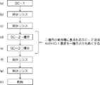
- FIG. 1 It is a flowchart which shows an example of the cleaning method of the semiconductor wafer of this invention. It is the figure which compared the number of the particle
- FIG. It is the figure which compared the number of the particle
- the present inventors first investigated the relationship between particle adhesion and zeta potential in a chemical bath containing SC-2 solution. Hereinafter, this relationship will be described with reference to FIGS.
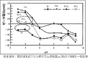
- FIG. 6 is a graph showing the relationship between the zeta potential ( ⁇ ) of particles and pH.
- Si, PSL (polystyrene latex), Si 3 N 4 and SiO 2 are listed as particles.
- FIG. 7 shows a photograph obtained by SEM (Scanning Electro Microscope) / EDX (Energy Dispersive X-ray spectroscopy) of SiO 2 surrounded by a broken line in FIG.
- FIG. 8 shows a photograph obtained by SEM / EDX of Si surrounded by a broken line in FIG.
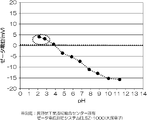
- FIG. 9 is a graph showing the relationship between the zeta potential ( ⁇ s) on the silicon wafer surface and pH.
- the zeta potential of particles such as SiO 2 and Si in the acidic region (around pH 2 to 4), that is, in the SC-2 tank containing the acidic solution is The absolute value is smaller than the area.
- the zeta potential on the surface of the silicon wafer is slightly near 0 on the plus side in the acidic region.
- Vr electric repulsive force
- the electric power between the silicon wafer surface and the particles is larger in the SC-2 tank (acidic) than in the SC-1 tank (alkaline). It can be seen that the repulsive force is weak.
- particles such as SiO 2 and Si having a small absolute value of the zeta potential in the acidic region tend to adhere to the silicon wafer after SC-2 cleaning.
- the SC-1 solution is an alkaline solution
- both the wafer surface and the surface charges of various particles have a negative charge, so that the adhesion of particles is suppressed by electrostatic repulsion.
- the SC-2 solution is an acidic solution, there is a problem that the surface charge of the wafer surface and the particles do not always have the same sign and the particles are likely to adhere during the SC-2 cleaning (see FIGS. 6 to 9 and the above theoretical formula). ).
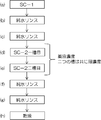
- FIG. 10 is a flowchart showing an example of a semiconductor wafer cleaning method when two SC-2 tanks are used and the composition of the SC-2 solution contained in the two tanks is the same.
- FIG. 10 is a flowchart showing an example of a semiconductor wafer cleaning method when two SC-2 tanks are used and the composition of the SC-2 solution contained in the two tanks is the same.
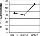
- FIG. 11 is a graph showing the relationship between the amount of increased particles and the HCl concentration before and after SC-2 cleaning.
- FIG. 11 illustrates the amount of increase in particles when the HCl concentration in the SC-2 solution is doubled or halved in both the first and second stages with respect to the REF condition.
- FIG. 12 is a graph showing the relationship between the amount of increased particles before and after the SC-2 cleaning and the SC-2 cleaning time.
- FIG. 12 illustrates the amount of increase in particles when the SC-2 cleaning time is doubled or halved in both the first and second stages with respect to the REF condition.
- FIG. 13 is a flowchart showing an example of a semiconductor wafer cleaning method when only one SC-2 tank is used.
- FIGS. 14 to 16 are diagrams showing the relationship between the number of particles per silicon wafer after SC-2 cleaning and the number of SC-2 tanks as relative values.
- FIG. 14 shows the number of particles of 26 nm or more measured using the particle inspection machine SP3 (manufactured by KLA-Tencor), and FIG. 15 shows particles of 45 nm or more measured using the particle inspection machine SP2 (manufactured by KLA-Tencor).
- FIG. 16 shows the number of particles of 120 nm or more measured using SP2.
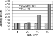
- FIG. 17 shows the relationship between the Al concentration on the silicon wafer surface after SC-2 cleaning and the cleaning batch of SC-2 cleaning, with one SC-2 tank and two SC-2 tanks. It is the figure compared relatively with the case where it was.
- the particle level improves when the SC-2 tank is reduced from two tanks to one tank.
- the Al detection level increases and the metal impurity level deteriorates.
- the inventors further studied to solve the above problems.
- a method of cleaning a semiconductor wafer using a chemical bath containing an SC-2 solution, wherein a plurality of the chemical baths are used, and the last used chemical solution among the SC-2 solutions contained in the plurality of chemical baths The present inventors have found that a semiconductor wafer cleaning method characterized by cleaning the semiconductor wafer by reducing the HCl concentration in the SC-2 solution contained in the bath to the lowest level, and has completed the present invention.
- the semiconductor wafer cleaning method of the present invention uses a plurality of SC-2 tanks when SC-2 cleaning a semiconductor wafer, and among the SC-2 solutions contained in the plurality of SC-2 tanks, This is a method for cleaning a semiconductor wafer by reducing the HCl concentration in the SC-2 solution contained in the SC-2 tank used last.
- the SC-2 solution contained in the last used chemical bath is made to have the lowest HCl concentration. 2 Particles are less likely to adhere to the surface of the semiconductor wafer after cleaning.
- the HCl concentration in the SC-2 solution contained in the second and subsequent chemical tanks is lower than that in the first tank.
- the semiconductor wafer to be cleaned in the present invention is not particularly limited, but an elemental semiconductor such as germanium or a compound semiconductor such as GaAs or InP can be used in addition to the silicon wafer.
- an elemental semiconductor such as germanium or a compound semiconductor such as GaAs or InP
- the method for cleaning a semiconductor wafer according to the present invention can be particularly suitably used for cleaning a silicon wafer.
- the present invention is not limited to this.
- three SC-2 tanks are used, and among the SC-2 solutions contained in the three SC-2 tanks, the SC-2 solutions contained in the first and second stage SC-2 tanks. It is also possible to clean the semiconductor wafer with the same HCl concentration in the SC-2 solution contained in the SC-2 tank used last and lower HCl concentration than in the first tank and the second tank.
- SC-2 three tanks of SC-2 are used, and the semiconductor wafer is cleaned with the relationship of HCl concentration in the SC-2 solution contained in these tanks of SC-2 being first tank> second tank> third tank. You can also. Note that the number of SC-2 tanks used in the present invention may be plural, but may be, for example, 2 to 5 tanks.
- the semiconductor wafer is SC-1 cleaned (FIG. 1 (a)).
- the SC-1 tank is filled with an aqueous solution of ammonium hydroxide and hydrogen peroxide (SC-1 solution), the semiconductor wafer is immersed in the SC-1 solution, and the semiconductor wafer is cleaned.
- the material of the SC-1 tank is not particularly limited, but for example, a quartz glass can be used.
- pure water rinsing is performed on the semiconductor wafer subjected to SC-1 cleaning (FIGS. 1B and 1C). At this time, ultrapure water can be used.
- pure water rinsing is performed in a total of four stages, but the conditions of these pure water rinsings may be the same or different.
- SC-2 cleaning is performed on the semiconductor wafer that has been subjected to pure water rinsing (FIG. 1 (d)).
- the SC-2 tank is filled with an aqueous solution of hydrochloric acid and hydrogen peroxide (SC-2 solution), the semiconductor wafer is immersed in the SC-2 solution, and the semiconductor wafer is cleaned.
- the material of the SC-2 tank is not particularly limited, but for example, a quartz glass can be used.
- the composition of the SC-2 solution contained in the first-stage SC-2 tank is not particularly limited, and cleaning can be performed as usual with an SC-2 solution having the same composition as the conventional one.
- the HCl concentration in the first-stage SC-2 solution needs to be higher than in the second tank described later.
- the HCl concentration in the first-stage SC-2 solution can be, for example, 0.3-2% by mass.
- the pH of the SC-2 solution in the first stage can be set to 1 to 4, for example.
- the concentration of H 2 O 2 in the first-stage SC-2 solution is not particularly limited, but can be, for example, 0.01 to 2% by mass.
- the temperature of the first-stage SC-2 solution is not particularly limited, but can be, for example, 40 to 90 ° C.
- the time for the first stage SC-2 cleaning is not particularly limited, but can be shorter than when only one SC-2 tank is used. This is because a plurality of SC-2 tanks are used in the present invention.
- This cleaning time can be, for example, 50 to 200 seconds.
- the second-stage SC-2 cleaning is performed on the semiconductor wafer that has been subjected to the first-stage SC-2 cleaning (FIG. 1E).
- the semiconductor wafer cleaning method shown in FIG. 1 two stages of SC-2 tanks are prepared, and the HCl concentration in the SC-2 solution contained in the latter stage tank is made lower than that of the preceding stage tank. In the latter stage, the amount of hydrochloric acid is made extremely small, but the pH is kept in the acidic region. As a result, since the HCl concentration in the SC-2 solution contained in the latter tank is lower than that in the former tank, the adhesion of particles is small, but since the second SC-2 solution is acidic, it cannot be completely removed in the former tank. Cleaning that removes metallic impurities is possible.
- the HCl concentration in the second stage SC-2 solution can be, for example, 0.001 to 0.2 mass%.
- the pH of the second stage SC-2 solution can be, for example, 2-6.
- the temperature of the second stage SC-2 solution is not particularly limited, but can be, for example, 40 to 90 ° C.
- the temperature of the first-stage SC-2 solution and the second-stage SC-2 solution may be the same or different.
- the time for cleaning the second stage SC-2 is not particularly limited, but can be, for example, 50 to 200 seconds.
- the time for the first-stage SC-2 cleaning and the second-stage SC-2 cleaning may be the same or different.
- the SC-2 solution may be replaced with a new solution for each batch, but in order to reduce costs, the same solution is used up to a predetermined number of batches, for example, 80 batches. May be. Even in such a case, since the present invention uses a plurality of SC-2 tanks, the metal impurity level is unlikely to deteriorate.
- the number of processing of one batch of semiconductor wafers is not particularly limited, but may be 5 to 25, for example.
- Example 1 According to the flow chart shown in FIG. 1, the 300 mm diameter boron-doped p-type single crystal silicon wafer after mirror polishing was cleaned. In the following examples and comparative examples, cleaning was performed by treating 25 silicon wafers as one batch.
- the silicon wafer was SC-1 cleaned using a quartz glass SC-1 bath (FIG. 1A).
- the silicon wafer subjected to pure water rinsing was SC-2 cleaned using quartz glass as the first SC-2 tank (FIG. 1 (d)).
- the first stage SC-2 cleaning conditions were as follows: HCl concentration was 0.4 mass%, H 2 O 2 concentration was 0.4 mass%, pH was 1, temperature was 80 ° C., and time was 125 seconds. did.
- the second stage SC-2 tank was made of quartz glass, and the silicon wafer subjected to the first stage SC-2 cleaning was subjected to the second stage SC-2 cleaning (FIG. 1 (e)). )).
- the second stage SC-2 cleaning conditions were as follows: HCl concentration was 0.2 mass%, H 2 O 2 concentration was 0.4 mass%, pH was 1, temperature was 80 ° C., and time was 125 seconds. It was.
- Example 2 The silicon wafer was cleaned in the same procedure as in Example 1 except that the HCl concentration in the second stage SC-2 cleaning was changed to 0.04 mass%.
- Example 3 The silicon wafer was cleaned in the same procedure as in Example 1 except that the HCl concentration in the second stage SC-2 cleaning was changed to 0.01 mass%.
- Example 4 The silicon wafer was prepared in the same procedure as in Example 1 except that the HCl concentration in the second SC-2 cleaning was changed to 0.01% by mass and the H 2 O 2 concentration was changed to 0.1% by mass. Washed.
- Example 1 A silicon wafer similar to that in Example 1 was cleaned according to the flowchart shown in FIG. Specifically, Example 1 except that the HCl concentration in the second-stage SC-2 cleaning was changed to 0.4 mass% (the HCl concentration was 0.4 mass% in both the first and second stages). The silicon wafer was cleaned in the same procedure as described above.
- Example 2 A silicon wafer similar to that in Example 1 was cleaned according to the flowchart shown in FIG. Specifically, the silicon wafer was cleaned in the same procedure as in Example 1 except that the second-stage SC-2 cleaning was not performed (only one SC-2 tank was used).
- the metal impurity levels and particle levels of the examples and comparative examples were evaluated as follows. First, particles before SC-2 cleaning (for example, after FIG. 1 (c) and before FIG. 1 (d) in the cleaning method of FIG. 1) are measured with a particle inspection machine SP3 (manufactured by KLA-Tencor). In addition, after the SC-2 cleaning under each condition (for example, after FIG. 1 (h) in the cleaning method of FIG. 1), the particles are measured again. The newly added point is defined as an increase point compared to before and after. In this example and the comparative example, the amount of particle deterioration was investigated at an increase point. Further, in the metal impurity analysis after SC-2 cleaning, the surface impurity concentration of the silicon wafer was evaluated by ICP-MS (Inductively Coupled Plasma-Mass Spectroscopy) analysis.
- ICP-MS Inductively Coupled Plasma-Mass Spectroscopy
- Table 1 shows the metal impurity level and particle level results. Table 1 shows the average of the results of two silicon wafers in the 80th batch cleaning.
- Comparative Example 1 there are two SC-2 tanks containing an SC-2 solution having a sufficient chemical concentration (the HCl concentration is 0.4% by mass in the first and second stages).
- the metal impurity level is good, but the amount of particle increase is large.
- Comparative Example 2 since the number of tanks is reduced from two to one, the amount of increase in particles is small, but a large amount of Al is detected, indicating that the metal removal ability is reduced.
- the HCl concentration in the second tank is set lower than that in the first tank, so the amount of increase in particles is small, but the Al detection amount is also below the detection lower limit, which is good.
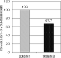
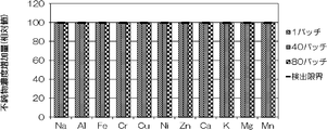
- Example 3 in which SC-2 cleaning is performed under conditions of low concentration in the latter stage is different from Comparative Example 1 in which SC-2 cleaning is performed under conditions of the same concentration in the previous stage and subsequent stage. In all particle sizes, the number of particles is reduced. Further, as shown in FIG. 5, under the conditions of Example 3, there is no deterioration of the metal impurity level even if the cleaning batch advances.
- 2 to 4 are diagrams comparing the number of particles per silicon wafer after SC-2 cleaning in Example 3 and Comparative Example 1 with relative values.
- 2 to 4 show the average of the results of 25 silicon wafers in the 80th batch cleaning.
- 2 shows the number of particles of 26 nm or more measured using SP3
- FIG. 3 shows the number of particles of 45 nm or more measured using SP2
- FIG. 4 shows the number of particles of 120 nm or more measured using SP2.
- FIG. 5 is a graph showing the relationship between the metal impurity concentration on the silicon wafer surface after SC-2 cleaning in Example 3 and the number of cleaning batches for SC-2 cleaning.
- the present invention is not limited to the above embodiment.
- the above-described embodiment is an exemplification, and the present invention has substantially the same configuration as the technical idea described in the claims of the present invention, and any device that exhibits the same function and effect is the present invention. It is included in the technical scope of the invention.
Landscapes
- Chemical & Material Sciences (AREA)
- Chemical Kinetics & Catalysis (AREA)
- Inorganic Chemistry (AREA)
- Life Sciences & Earth Sciences (AREA)
- Engineering & Computer Science (AREA)
- Oil, Petroleum & Natural Gas (AREA)
- Wood Science & Technology (AREA)
- Organic Chemistry (AREA)
- General Chemical & Material Sciences (AREA)
- Cleaning Or Drying Semiconductors (AREA)
Abstract
本発明は、SC-2溶液を含む薬液槽を用いて半導体ウェーハを洗浄する方法であって、前記薬液槽を複数用い、該複数の薬液槽に含まれるSC-2溶液のうち、最後に用いる薬液槽に含まれるSC-2溶液中のHCl濃度を最も低くして前記半導体ウェーハを洗浄することを特徴とする半導体ウェーハの洗浄方法である。これにより、半導体ウェーハをSC-2洗浄する際に、半導体ウェーハ表面における金属不純物レベルを悪化させることなく、パーティクルレベルを向上させることができる半導体ウェーハの洗浄方法が提供される。
Description
本発明は、半導体ウェーハの洗浄方法に関する。
シリコンウェーハ等の半導体ウェーハの洗浄方法として、従来からRCA洗浄と呼ばれるSC-1(Standard Cleaning 1)溶液、SC-2(Standard Cleaning 2)溶液を使用した洗浄方法が広く用いられている。SC-1溶液は水酸化アンモニウムと過酸化水素の水溶液であり、半導体ウェーハ表面のパーティクル除去性能が非常に優れているという特徴を有している。SC-2溶液は塩酸と過酸化水素の水溶液であり、金属不純物除去の役割を担っている。
例えば、特許文献1には、SC-1溶液及びSC-2溶液を使用した半導体ウェーハの洗浄方法として、SC-2溶液による洗浄(SC-2洗浄)時に半導体ウェーハの表面に陰イオンが付着することを防止するために、陽イオン化した金属を半導体ウェーハの表面に残留させるようにSC-1溶液で洗浄(SC-1洗浄)する方法が記載されている。
SC-1溶液はアルカリ性溶液であるため、SC-1洗浄時にはウェーハ表面と各種パーティクルの表面電荷が共にマイナスの電荷を持つため静電反発力によりパーティクルの付着が抑制される。しかしSC-2溶液は酸性溶液であるため、SC-2洗浄時にはウェーハ表面とパーティクルの表面電荷が必ずしも同符号とならずパーティクルが付着しやすいという問題がある。また、SC-2溶液に添加するHClの濃度が濃いほど、SC-2洗浄時間が長いほどウェーハ表面にパーティクルが付着しやすくなってしまう。SC-2洗浄時間を短く、SC-2溶液中のHCl濃度を薄くすることでパーティクルレベルの悪化を抑えることは可能だが、この場合、酸による金属除去効果が低下するので、金属不純物レベルが悪化してしまう。
本発明は、上記問題点に鑑みてなされたものであって、半導体ウェーハをSC-2洗浄する際に、半導体ウェーハ表面における金属不純物レベルを悪化させることなく、パーティクルレベルを向上させることができる半導体ウェーハの洗浄方法を提供することを目的とする。
上記目的を達成するために、本発明では、SC-2溶液を含む薬液槽を用いて半導体ウェーハを洗浄する方法であって、
前記薬液槽を複数用い、該複数の薬液槽に含まれるSC-2溶液のうち、最後に用いる薬液槽に含まれるSC-2溶液中のHCl濃度を最も低くして前記半導体ウェーハを洗浄することを特徴とする半導体ウェーハの洗浄方法を提供する。
前記薬液槽を複数用い、該複数の薬液槽に含まれるSC-2溶液のうち、最後に用いる薬液槽に含まれるSC-2溶液中のHCl濃度を最も低くして前記半導体ウェーハを洗浄することを特徴とする半導体ウェーハの洗浄方法を提供する。
このような半導体ウェーハの洗浄方法であれば、複数の薬液槽に含まれるSC-2溶液のうち、最後に用いる薬液槽に含まれるSC-2溶液中のHCl濃度を最も低くするため、SC-2洗浄後の半導体ウェーハ表面にパーティクルが付着しにくくなる。また、最後に用いる薬液槽より前の槽は、HCl濃度が最後の槽より濃いので、金属不純物の除去も十分に行うことができる上、複数の薬液槽を用いてSC-2洗浄を行うことにより、一段目の薬液槽で落とし切れなかった金属不純物を後の段で除去することができる。なお、以下では、SC-1溶液を含む薬液槽をSC-1槽、SC-2溶液を含む薬液槽をSC-2槽とも呼称する。
また、二段目以降の薬液槽に含まれるSC-2溶液中のHCl濃度を一槽目よりも低くすることが好ましい。
このような半導体ウェーハの洗浄方法であれば、金属不純物を確実に除去できるとともに、半導体ウェーハ表面のパーティクルレベルが悪化してしまうことをより確実に抑制することができる。
また、前記半導体ウェーハをシリコンウェーハとすることが好ましい。
本発明の半導体ウェーハの洗浄方法は、シリコンウェーハを洗浄するのに特に好適に用いることができる。
本発明の半導体ウェーハの洗浄方法であれば、金属不純物レベルを悪化させることなく、パーティクルレベルを向上させることができる。
以下、本発明をより詳細に説明する。
上記のように、半導体ウェーハをSC-2洗浄する際に、半導体ウェーハ表面における金属不純物レベルを悪化させることなく、パーティクルレベルを向上させることができる半導体ウェーハの洗浄方法が求められている。
本発明者らは、まず、SC-2溶液を含む薬液槽内でのパーティクルの付着とゼータ電位の関係について調査した。以下、図6~9を参照してこの関係について説明する。
図6はパーティクルのゼータ電位(ψ)とpHの関係を示す図である。図6中には、パーティクルとしてSi、PSL(ポリスチレンラテックス)、Si3N4及びSiO2が挙げられている。また、図7に、図6中の破線で囲まれたSiO2のSEM(Scanning Electro Microscopy)/EDX(Energy Dispersive X-ray spectroscopy)で得られた写真を示す。また、図8に図6中の破線で囲まれたSiのSEM/EDXで得られた写真を示す。また、図9はシリコンウェーハ表面のゼータ電位(ψs)とpHの関係を示す図である。
図6の破線で囲まれた部分に示すように、酸性領域(pH2~4付近)における、すなわち、酸性の溶液を含むSC-2槽内におけるSiO2やSi等のパーティクルのゼータ電位は、アルカリ領域に比べ絶対値が小さい。また、図9の破線で囲まれた部分に示すように、シリコンウェーハ表面のゼータ電位は酸性領域ではややプラス側の0付近である。ここで、電気的反発力(Vr)の理論式は以下の通りであるため、SC-2槽内(酸性)ではSC-1槽内(アルカリ性)に比べ、シリコンウェーハ表面とパーティクルとの電気的反発力が弱いことが分かる。特に、酸性領域におけるゼータ電位の絶対値が小さいSiO2やSi等のパーティクルは、SC-2洗浄後のシリコンウェーハに付着しやすい。

また、SC-1溶液はアルカリ性溶液であるため、SC-1洗浄時にはウェーハ表面と各種パーティクルの表面電荷が共にマイナスの電荷を持つため静電反発力によりパーティクルの付着が抑制される。しかしSC-2溶液は酸性溶液であるため、SC-2洗浄時にはウェーハ表面とパーティクルの表面電荷が必ずしも同符号とならずパーティクルが付着しやすいという問題がある(図6~9及び上記理論式参照)。
本発明者らは、次に、SC-2槽の各条件を変えて洗浄を行い、パーティクルの増加量を調査した。以下、図10~12を参照してSC-2洗浄条件とパーティクル増加量の関係について説明する。図10はSC-2槽を二槽用い、二槽に含まれるSC-2溶液の組成を同じにした場合の半導体ウェーハの洗浄方法の一例を示すフロー図である。SC-2洗浄のREF条件(参照条件)は、一段目のSC-2槽、二段目のSC-2槽共に、濃度(体積比)をHCl:H2O2:H2O=1:1:100とし、温度を80℃とし、時間を125秒とした。また、図11はSC-2洗浄前後におけるパーティクル増加量とHCl濃度の関係を示す図である。図11には、REF条件の場合、REF条件に対してSC-2溶液中のHCl濃度を一段目、二段目共に2倍又は1/2にした場合のパーティクル増加量を図示してある。また、図12はSC-2洗浄前後におけるパーティクル増加量とSC-2洗浄時間の関係を示す図である。図12には、REF条件の場合、REF条件に対してSC-2洗浄時間を一段目、二段目共に2倍又は1/2にした場合のパーティクル増加量を図示してある。
図10~12に示すように、SC-2溶液に添加するHClの濃度が濃いほど、SC-2洗浄時間が長いほどウェーハ表面にパーティクルが付着しやすくなってしまう。
本発明者らは、更に、SC-2槽を二槽から一槽に削減してSC-2洗浄を行った。以下、図13~17を参照してSC-2槽を一槽のみ用い、シリコンウェーハをSC-2洗浄した場合の洗浄後のパーティクルレベルと金属不純物レベルの関係について説明する。なお、本調査においてSC-2槽を二槽から一槽に削減する以外の洗浄条件は、図10のREF条件の場合と同じとした。図13はSC-2槽を一槽のみ用いた場合の半導体ウェーハの洗浄方法の一例を示すフロー図である。また、図14~16はSC-2洗浄後におけるシリコンウェーハ1枚当たりのパーティクルの数とSC-2槽の数との関係を相対値で示す図である。図14はパーティクル検査機SP3(KLA-Tencor社製)を用いて測定した26nm以上のパーティクルの数について、図15はパーティクル検査機SP2(KLA-Tencor社製)を用いて測定した45nm以上のパーティクルの数について、図16はSP2を用いて測定した120nm以上のパーティクルの数について、それぞれ示している。また、図17は、SC-2洗浄後におけるシリコンウェーハ表面のAl濃度とSC-2洗浄の洗浄バッチとの関係を、SC-2槽を一槽用いた場合とSC-2槽を二槽用いた場合とで相対比較した図である。
図14~17に示すように、SC-2槽を二槽から一槽に減らすとパーティクルレベルが改善する。しかしながら、この場合、洗浄バッチが増えるとAl検出レベルが増加し、金属不純物レベルが悪化する。
図10~17に示すように、SC-2洗浄時間を短く、SC-2溶液中のHCl濃度を薄くすることでパーティクルレベルの悪化を抑えることは可能だが、この場合、酸による金属除去効果が低下するので、金属不純物レベルが悪化してしまう。
本発明者らは、上記問題点を解決するために、更に検討を行った。その結果、SC-2溶液を含む薬液槽を用いて半導体ウェーハを洗浄する方法であって、前記薬液槽を複数用い、該複数の薬液槽に含まれるSC-2溶液のうち、最後に用いる薬液槽に含まれるSC-2溶液中のHCl濃度を最も低くして前記半導体ウェーハを洗浄することを特徴とする半導体ウェーハの洗浄方法が、上記課題を解決できることを見出し、本発明を完成させた。
以下、本発明の実施の形態について具体的に説明するが、本発明はこれらに限定されるものではない。
上記のように、本発明の半導体ウェーハの洗浄方法は、半導体ウェーハをSC-2洗浄する際にSC-2槽を複数用い、該複数のSC-2槽に含まれるSC-2溶液のうち、最後に用いるSC-2槽に含まれるSC-2溶液中のHCl濃度を最も低くして半導体ウェーハを洗浄する方法である。このような半導体ウェーハの洗浄方法であれば、複数の薬液槽に含まれるSC-2溶液のうち、最後に用いる薬液槽に含まれるSC-2溶液中のHCl濃度を最も低くするため、SC-2洗浄後の半導体ウェーハ表面にパーティクルが付着しにくくなる。また、最後に用いる薬液槽より前の槽は、HCl濃度が最後の槽より濃いので、金属不純物の除去も十分に行うことができる上、複数の薬液槽を用いてSC-2洗浄を行うことにより、一段目の薬液槽で落とし切れなかった金属不純物を後の段で除去することができる。
この場合、二段目以降の薬液槽に含まれるSC-2溶液中のHCl濃度を一槽目よりも低くすることが好ましい。これにより、金属不純物を確実に除去できるとともに、半導体ウェーハ表面のパーティクルレベルが悪化してしまうことをより確実に抑制することができる。
本発明における洗浄される半導体ウェーハは特に限定はされないが、シリコンウェーハの他に、ゲルマニウムのような元素半導体やGaAs、InPのような化合物半導体等でも使用することができる。中でも、本発明の半導体ウェーハの洗浄方法は、シリコンウェーハを洗浄するのに特に好適に用いることができる。
以下、図1を参照して、本発明の半導体ウェーハの洗浄方法について説明する。ここでは、SC-2槽を二槽用い、二槽のSC-2槽に含まれるSC-2溶液のうち、二段目のSC-2槽に含まれるSC-2溶液中のHCl濃度を一槽目よりも低くして半導体ウェーハを洗浄する場合について説明するが、本発明はこれに限定されるものではない。例えば、本発明では、SC-2槽を三槽用い、三槽のSC-2槽に含まれるSC-2溶液のうち、一段目と二段目のSC-2槽に含まれるSC-2溶液中のHCl濃度を同じにし、最後に用いるSC-2槽に含まれるSC-2溶液中のHCl濃度を一槽目と二槽目よりも低くして半導体ウェーハを洗浄することもできる。また、SC-2槽を三槽用い、これらのSC-2槽に含まれるSC-2溶液中のHCl濃度の大小関係を一槽目>二槽目>三槽目として半導体ウェーハを洗浄することもできる。なお、本発明において用いるSC-2槽の数は複数であれば良いが、例えば、2~5槽とすることができる。
まず、半導体ウェーハをSC-1洗浄する(図1(a))。例えば、SC-1槽内に、水酸化アンモニウムと過酸化水素の水溶液(SC-1溶液)を満たし、半導体ウェーハをSC-1溶液に浸漬させ、半導体ウェーハを洗浄する。SC-1槽の材質は特に限定されないが、例えば、石英ガラス製のものを用いることができる。
次に、SC-1洗浄を施した半導体ウェーハに対して純水リンスを行う(図1(b)、(c))。この際、超純水を用いることができる。図1に示す半導体ウェーハの洗浄方法においては、純水リンスを計四段行うが、これらの純水リンスの条件は同じであっても、異なっていてもよい。
次に、純水リンスを施した半導体ウェーハをSC-2洗浄する(図1(d))。例えば、SC-2槽内に、塩酸と過酸化水素の水溶液(SC-2溶液)を満たし、半導体ウェーハをSC-2溶液に浸漬させ、半導体ウェーハを洗浄する。SC-2槽の材質は特に限定されないが、例えば、石英ガラス製のものを用いることができる。
一段目のSC-2槽に含まれるSC-2溶液の組成は特に限定されず、従来と同組成のSC-2溶液で従来通り洗浄を行うことができる。但し、一段目のSC-2溶液中のHCl濃度は、後述する二槽目よりも高い必要がある。一段目のSC-2溶液中のHCl濃度は、例えば、0.3~2質量%とすることができる。一段目のSC-2溶液のpHは、例えば、1~4とすることができる。
一段目のSC-2溶液中のH2O2濃度は特に限定されないが、例えば、0.01~2質量%とすることができる。
一段目のSC-2溶液の温度は特に限定されないが、例えば、40~90℃とすることができる。
一段目のSC-2洗浄の時間は特に限定されないが、SC-2槽を一槽のみ用いる場合よりも短くすることができる。本発明では、SC-2槽を複数用いるためである。この洗浄時間は、例えば、50~200秒とすることができる。
次に、一段目のSC-2洗浄を施した半導体ウェーハに二段目のSC-2洗浄を施す(図1(e))。図1に示す半導体ウェーハの洗浄方法においては、SC-2槽を2段用意して、後段槽に含まれるSC-2溶液中のHCl濃度を前段槽より低くする。後段では塩酸を極微量にするが、pHを酸性領域にしておく。これにより、後段槽に含まれるSC-2溶液中のHCl濃度が前段槽よりも低いためにパーティクルの付着は少ないが、二段目のSC-2溶液は酸性であるので前段槽で落とし切れなかった金属不純物を除去する洗浄が可能となる。二段目のSC-2溶液中のHCl濃度は、例えば、0.001~0.2質量%とすることができる。二段目のSC-2溶液のpHは、例えば、2~6とすることができる。
二段目のSC-2溶液の温度は特に限定されないが、例えば、40~90℃とすることができる。一段目のSC-2溶液と二段目のSC-2溶液の温度は同じであっても、異なっていてもよい。
二段目のSC-2洗浄の時間は特に限定されないが、例えば、50~200秒とすることができる。一段目のSC-2洗浄と二段目のSC-2洗浄の時間は同じであっても、異なっていてもよい。
本発明においてバッチ処理により半導体ウェーハを洗浄する場合、SC-2溶液はバッチごとに新しい溶液に換えても良いが、コストを減らすために、所定のバッチ数、例えば、80バッチまで同じ溶液を用いても良い。このような場合であっても、本発明であればSC-2槽を複数用いるため、金属不純物レベルが悪化しにくい。なお、1バッチの半導体ウェーハの処理数は特に限定されないが、例えば、5~25枚とすることができる。
次に、二段目のSC-2洗浄を施した半導体ウェーハに対して純水リンスを行う(図1(f)、(g))。
次に、四段目の純水リンスを施した半導体ウェーハを乾燥させる(図1(h))。
以下、実施例及び比較例を示して本発明をより具体的に説明するが、本発明は下記の実施例に限定されるものではない。
(実施例1)
図1に示すフロー図に従って鏡面研磨後の直径300mmボロンドープp型単結晶シリコンウェーハを洗浄した。なお、以下に示す実施例及び比較例において、洗浄は、シリコンウェーハ25枚を1バッチとして処理した。
図1に示すフロー図に従って鏡面研磨後の直径300mmボロンドープp型単結晶シリコンウェーハを洗浄した。なお、以下に示す実施例及び比較例において、洗浄は、シリコンウェーハ25枚を1バッチとして処理した。
まず、石英ガラス製のSC-1槽を用いてシリコンウェーハをSC-1洗浄した(図1(a))。SC-1洗浄の条件は、濃度(体積比)をNH4OH:H2O2:H2O=1:1:20とし、温度を70℃とし、時間を125秒とした。
次に、SC-1洗浄を施したシリコンウェーハに対して超純水を用いて純水リンスを2段行った(図1(b)、(c))。
次に、一槽目のSC-2槽として石英ガラス製のものを用いて、純水リンスを施したシリコンウェーハをSC-2洗浄した(図1(d))。一段目のSC-2洗浄の条件は、HCl濃度を0.4質量%とし、H2O2濃度を0.4質量%とし、pHを1とし、温度を80℃とし、時間を125秒とした。
次に、二槽目のSC-2槽として石英ガラス製のものを用いて、一段目のSC-2洗浄を施したシリコンウェーハに二段目のSC-2洗浄を施した(図1(e))。二段目のSC-2洗浄の条件は、HCl濃度を0.2質量%とし、H2O2濃度を0.4質量%とし、pHを1とし、温度を80℃とし、時間を125秒とした。
次に、二段目のSC-2洗浄を施したシリコンウェーハに対して超純水を用いて純水リンスを2段行った(図1(f)、(g))。
次に、四段目の純水リンスを施したシリコンウェーハを乾燥させた(図1(h))。
(実施例2)
二段目のSC-2洗浄におけるHCl濃度を0.04質量%に変更したこと以外、実施例1と同様の手順で、シリコンウェーハを洗浄した。
二段目のSC-2洗浄におけるHCl濃度を0.04質量%に変更したこと以外、実施例1と同様の手順で、シリコンウェーハを洗浄した。
(実施例3)
二段目のSC-2洗浄におけるHCl濃度を0.01質量%に変更したこと以外、実施例1と同様の手順で、シリコンウェーハを洗浄した。
二段目のSC-2洗浄におけるHCl濃度を0.01質量%に変更したこと以外、実施例1と同様の手順で、シリコンウェーハを洗浄した。
(実施例4)
二段目のSC-2洗浄におけるHCl濃度を0.01質量%に変更し、H2O2濃度を0.1質量%に変更したこと以外、実施例1と同様の手順で、シリコンウェーハを洗浄した。
二段目のSC-2洗浄におけるHCl濃度を0.01質量%に変更し、H2O2濃度を0.1質量%に変更したこと以外、実施例1と同様の手順で、シリコンウェーハを洗浄した。
(比較例1)
図10に示すフロー図に従って実施例1と同様のシリコンウェーハを洗浄した。具体的には、二段目のSC-2洗浄におけるHCl濃度を0.4質量%に変更した(HCl濃度を一段目、二段目共に0.4質量%とした)こと以外、実施例1と同様の手順で、シリコンウェーハを洗浄した。
図10に示すフロー図に従って実施例1と同様のシリコンウェーハを洗浄した。具体的には、二段目のSC-2洗浄におけるHCl濃度を0.4質量%に変更した(HCl濃度を一段目、二段目共に0.4質量%とした)こと以外、実施例1と同様の手順で、シリコンウェーハを洗浄した。
(比較例2)
図13に示すフロー図に従って実施例1と同様のシリコンウェーハを洗浄した。具体的には、二段目のSC-2洗浄を行わない(SC-2槽を一槽のみ用いる)こと以外、実施例1と同様の手順で、シリコンウェーハを洗浄した。
図13に示すフロー図に従って実施例1と同様のシリコンウェーハを洗浄した。具体的には、二段目のSC-2洗浄を行わない(SC-2槽を一槽のみ用いる)こと以外、実施例1と同様の手順で、シリコンウェーハを洗浄した。
実施例及び比較例の金属不純物レベル及びパーティクルレベルは以下のようにして評価した。まず、パーティクル検査機SP3(KLA-Tencor社製)でSC-2洗浄前(例えば、図1の洗浄方法においては図1(c)の後かつ図1(d)の前)のパーティクルを測定しておき、各条件でSC-2洗浄後(例えば、図1の洗浄方法においては図1(h)の後)、再度パーティクルを測定する。前後で比較して新たに付着していた点を増加点とする。本実施例及び比較例では増加点でパーティクルの悪化量を調査した。また、SC-2洗浄後の金属不純物分析はシリコンウェーハの表面不純物濃度をICP-MS(Inductively Coupled Plasma - Mass Spectroscopy)分析により評価した。
金属不純物レベル及びパーティクルレベルの結果を表1に示す。なお、表1には、80バッチ目の洗浄におけるシリコンウェーハ2枚の結果の平均を示している。
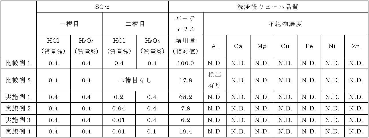
表1に示すように、比較例1では十分な薬液濃度のSC-2溶液を含むSC-2槽が2槽ある(HCl濃度を一段目、二段目共に0.4質量%とした)ため金属不純物レベルは良好であるが、パーティクル増加量は多い。比較例2では槽を二槽から一槽に減らしているため、パーティクル増加量は少ないが、Alが多く検出されており、金属除去能力が低下していることがわかる。これらに対して実施例1~4では二槽目のHCl濃度を一槽目より低く設定しているのでパーティクル増加量が少ないが、Al検出量も検出下限以下であり良好である。
また、図2~4に示すように、SC-2洗浄を後段低濃度の条件で行う実施例3は、SC-2洗浄を前段と後段とで同濃度の条件で行う比較例1と比べて、全ての粒径でパーティクルの数が少なくなっている。また、図5に示すように、実施例3の条件では、洗浄バッチが進んでも金属不純物レベルの悪化もない。
なお、図2~4は実施例3と比較例1とでSC-2洗浄後におけるシリコンウェーハ1枚当たりのパーティクルの数を相対値で比較した図である。図2~4では、80バッチ目の洗浄におけるシリコンウェーハ25枚の結果の平均を示している。図2はSP3を用いて測定した26nm以上のパーティクルの数について、図3はSP2を用いて測定した45nm以上のパーティクルの数について、図4はSP2を用いて測定した120nm以上のパーティクルの数について、それぞれ示している。また、図5は、実施例3のSC-2洗浄後におけるシリコンウェーハ表面の金属不純物濃度とSC-2洗浄の洗浄バッチ数との関係を示す図である。
なお、本発明は、上記実施形態に限定されるものではない。上記実施形態は、例示であり、本発明の特許請求の範囲に記載された技術的思想と実質的に同一な構成を有し、同様な作用効果を奏するものは、いかなるものであっても本発明の技術的範囲に包含される。
Claims (3)
- SC-2溶液を含む薬液槽を用いて半導体ウェーハを洗浄する方法であって、
前記薬液槽を複数用い、該複数の薬液槽に含まれるSC-2溶液のうち、最後に用いる薬液槽に含まれるSC-2溶液中のHCl濃度を最も低くして前記半導体ウェーハを洗浄することを特徴とする半導体ウェーハの洗浄方法。 - 二段目以降の薬液槽に含まれるSC-2溶液中のHCl濃度を一槽目よりも低くすることを特徴とする請求項1に記載の半導体ウェーハの洗浄方法。
- 前記半導体ウェーハをシリコンウェーハとすることを特徴とする請求項1又は請求項2に記載の半導体ウェーハの洗浄方法。
Priority Applications (5)
| Application Number | Priority Date | Filing Date | Title |
|---|---|---|---|
| SG11201807140QA SG11201807140QA (en) | 2016-03-18 | 2017-02-22 | Method for cleaning semiconductor wafer |
| KR1020187026568A KR102474557B1 (ko) | 2016-03-18 | 2017-02-22 | 반도체 웨이퍼의 세정방법 |
| CN201780012827.6A CN108701603A (zh) | 2016-03-18 | 2017-02-22 | 半导体晶圆的洗净方法 |
| DE112017000938.3T DE112017000938T8 (de) | 2016-03-18 | 2017-02-22 | Verfahren zum Reinigen eines Halbleiterwafers |
| US16/079,264 US10692714B2 (en) | 2016-03-18 | 2017-02-22 | Method for cleaning semiconductor wafer |
Applications Claiming Priority (2)
| Application Number | Priority Date | Filing Date | Title |
|---|---|---|---|
| JP2016055294A JP6424183B2 (ja) | 2016-03-18 | 2016-03-18 | 半導体ウェーハの洗浄方法 |
| JP2016-055294 | 2016-03-18 |
Publications (1)
| Publication Number | Publication Date |
|---|---|
| WO2017159246A1 true WO2017159246A1 (ja) | 2017-09-21 |
Family
ID=59850723
Family Applications (1)
| Application Number | Title | Priority Date | Filing Date |
|---|---|---|---|
| PCT/JP2017/006512 Ceased WO2017159246A1 (ja) | 2016-03-18 | 2017-02-22 | 半導体ウェーハの洗浄方法 |
Country Status (8)
| Country | Link |
|---|---|
| US (1) | US10692714B2 (ja) |
| JP (1) | JP6424183B2 (ja) |
| KR (1) | KR102474557B1 (ja) |
| CN (1) | CN108701603A (ja) |
| DE (1) | DE112017000938T8 (ja) |
| SG (1) | SG11201807140QA (ja) |
| TW (1) | TWI767902B (ja) |
| WO (1) | WO2017159246A1 (ja) |
Families Citing this family (4)
| Publication number | Priority date | Publication date | Assignee | Title |
|---|---|---|---|---|
| JP6424183B2 (ja) * | 2016-03-18 | 2018-11-14 | 信越半導体株式会社 | 半導体ウェーハの洗浄方法 |
| KR102713031B1 (ko) * | 2020-07-02 | 2024-10-07 | 창신 메모리 테크놀로지즈 아이엔씨 | 반도체 구조의 처리 방법 및 형성 방법 |
| CN113889405B (zh) | 2020-07-02 | 2024-07-05 | 长鑫存储技术有限公司 | 半导体结构的处理方法及形成方法 |
| CN112452906A (zh) * | 2020-09-29 | 2021-03-09 | 威科赛乐微电子股份有限公司 | 一种研磨后晶片的清洗方法 |
Citations (4)
| Publication number | Priority date | Publication date | Assignee | Title |
|---|---|---|---|---|
| JPH11283947A (ja) * | 1998-03-27 | 1999-10-15 | Dainippon Screen Mfg Co Ltd | 基板処理装置および基板処理方法 |
| JP2001053016A (ja) * | 1999-08-04 | 2001-02-23 | Toshiba Corp | 半導体装置の製造方法 |
| JP2005210075A (ja) * | 2003-12-25 | 2005-08-04 | Matsushita Electric Ind Co Ltd | 半導体ウエハの洗浄方法 |
| JP2015041753A (ja) * | 2013-08-23 | 2015-03-02 | 株式会社東芝 | ウェハの洗浄方法 |
Family Cites Families (18)
| Publication number | Priority date | Publication date | Assignee | Title |
|---|---|---|---|---|
| JP2643814B2 (ja) * | 1993-12-24 | 1997-08-20 | 日本電気株式会社 | 半導体基板の洗浄方法 |
| US6240933B1 (en) * | 1997-05-09 | 2001-06-05 | Semitool, Inc. | Methods for cleaning semiconductor surfaces |
| TW426874B (en) * | 1998-10-14 | 2001-03-21 | United Microelectronics Corp | Method for cleaning a semiconductor wafer |
| US7456113B2 (en) * | 2000-06-26 | 2008-11-25 | Applied Materials, Inc. | Cleaning method and solution for cleaning a wafer in a single wafer process |
| US6589356B1 (en) * | 2000-09-29 | 2003-07-08 | Taiwan Semiconductor Manufacturing Co., Ltd | Method for cleaning a silicon-based substrate without NH4OH vapor damage |
| US6503333B2 (en) * | 2000-11-30 | 2003-01-07 | Taiwan Semiconductor Manufacturing Company, Ltd | Method for cleaning semiconductor wafers with ozone-containing solvent |
| JP2002261062A (ja) * | 2001-03-05 | 2002-09-13 | Texas Instr Japan Ltd | 半導体ウェハ上の粒子を除去する方法及び装置 |
| TW512445B (en) * | 2001-04-30 | 2002-12-01 | Macronix Int Co Ltd | Method for cleaning semiconductor wafer |
| US20030106572A1 (en) * | 2001-12-12 | 2003-06-12 | Hirohiko Nishiki | System and method for ozonated water cleaning |
| TW533497B (en) * | 2002-04-30 | 2003-05-21 | Silicon Integrated Sys Corp | Cleaning method of wet cleaning device |
| CN1464533A (zh) * | 2002-06-26 | 2003-12-31 | 矽统科技股份有限公司 | 湿式洗净装置 |
| US7071077B2 (en) * | 2003-03-26 | 2006-07-04 | S.O.I.Tec Silicon On Insulator Technologies S.A. | Method for preparing a bonding surface of a semiconductor layer of a wafer |
| JP4179098B2 (ja) | 2003-08-13 | 2008-11-12 | 株式会社Sumco | 半導体ウェーハの洗浄方法 |
| KR20050065312A (ko) | 2003-12-25 | 2005-06-29 | 마츠시타 덴끼 산교 가부시키가이샤 | 반도체웨이퍼의 세정방법 |
| US20050177267A1 (en) * | 2004-02-10 | 2005-08-11 | Taiwan Semiconductor Manufacturing Co., Ltd. | Tank scheduling optimization for replicated chemical in a semiconductor manufacturing wet bench |
| JP5789400B2 (ja) * | 2011-04-12 | 2015-10-07 | 東京エレクトロン株式会社 | 液処理方法及び液処理装置 |
| US9561982B2 (en) * | 2013-04-30 | 2017-02-07 | Corning Incorporated | Method of cleaning glass substrates |
| JP6424183B2 (ja) * | 2016-03-18 | 2018-11-14 | 信越半導体株式会社 | 半導体ウェーハの洗浄方法 |
-
2016
- 2016-03-18 JP JP2016055294A patent/JP6424183B2/ja active Active
-
2017
- 2017-02-22 SG SG11201807140QA patent/SG11201807140QA/en unknown
- 2017-02-22 US US16/079,264 patent/US10692714B2/en active Active
- 2017-02-22 CN CN201780012827.6A patent/CN108701603A/zh active Pending
- 2017-02-22 KR KR1020187026568A patent/KR102474557B1/ko active Active
- 2017-02-22 WO PCT/JP2017/006512 patent/WO2017159246A1/ja not_active Ceased
- 2017-02-22 DE DE112017000938.3T patent/DE112017000938T8/de active Active
- 2017-03-01 TW TW106106583A patent/TWI767902B/zh active
Patent Citations (4)
| Publication number | Priority date | Publication date | Assignee | Title |
|---|---|---|---|---|
| JPH11283947A (ja) * | 1998-03-27 | 1999-10-15 | Dainippon Screen Mfg Co Ltd | 基板処理装置および基板処理方法 |
| JP2001053016A (ja) * | 1999-08-04 | 2001-02-23 | Toshiba Corp | 半導体装置の製造方法 |
| JP2005210075A (ja) * | 2003-12-25 | 2005-08-04 | Matsushita Electric Ind Co Ltd | 半導体ウエハの洗浄方法 |
| JP2015041753A (ja) * | 2013-08-23 | 2015-03-02 | 株式会社東芝 | ウェハの洗浄方法 |
Also Published As
| Publication number | Publication date |
|---|---|
| US20190066999A1 (en) | 2019-02-28 |
| SG11201807140QA (en) | 2018-09-27 |
| DE112017000938T5 (de) | 2019-01-03 |
| JP6424183B2 (ja) | 2018-11-14 |
| TW201801167A (zh) | 2018-01-01 |
| KR102474557B1 (ko) | 2022-12-06 |
| TWI767902B (zh) | 2022-06-21 |
| US10692714B2 (en) | 2020-06-23 |
| JP2017168785A (ja) | 2017-09-21 |
| DE112017000938T8 (de) | 2019-03-07 |
| CN108701603A (zh) | 2018-10-23 |
| KR20180125473A (ko) | 2018-11-23 |
Similar Documents
| Publication | Publication Date | Title |
|---|---|---|
| JP4752270B2 (ja) | 洗浄液及びそれを用いた洗浄方法 | |
| JP5533624B2 (ja) | 半導体ウェーハの洗浄方法 | |
| JP6424183B2 (ja) | 半導体ウェーハの洗浄方法 | |
| JP2002069495A (ja) | 洗浄剤組成物 | |
| JP3957264B2 (ja) | 半導体基板の洗浄方法 | |
| WO2012172724A1 (ja) | 半導体ウェーハの洗浄方法 | |
| JP2013251461A (ja) | 半導体ウェーハの洗浄方法 | |
| CN113518817B (zh) | 氮化硅膜蚀刻组合物 | |
| US6884721B2 (en) | Silicon wafer storage water and silicon wafer storage method | |
| KR20140091327A (ko) | 웨이퍼 세정 방법 | |
| US20120129344A1 (en) | Process and apparatus for removal of contaminating material from substrates | |
| KR20210015762A (ko) | 실리콘 웨이퍼의 세정방법 | |
| US20040266191A1 (en) | Process for the wet-chemical surface treatment of a semiconductor wafer | |
| TWI755496B (zh) | 半導體晶圓的洗淨方法 | |
| JP4857738B2 (ja) | 半導体ウエーハの洗浄方法および製造方法 | |
| JPH08306651A (ja) | アルカリ性洗浄組成物及びそれを用いた基板の洗浄方法 | |
| JP2001244228A (ja) | 半導体基板の洗浄液及び洗浄方法 | |
| JP6784237B2 (ja) | シリコンエピタキシャルウェーハの製造方法 | |
| CN113544248A (zh) | 半导体晶片清洗液组合物及利用其的清洗方法 | |
| JP2688293B2 (ja) | ウェーハの表面洗浄方法 | |
| TW404852B (en) | Method for cleaning semiconductor wafer | |
| JPH0689888A (ja) | 半導体ウェーハの洗浄方法 | |
| JP2007123383A (ja) | 半導体ウエーハの製造方法及び半導体ウエーハの洗浄方法 | |
| KR20230100380A (ko) | Cmp 후 세정액 조성물 | |
| JP2008181941A (ja) | 金属系不純物の除去方法 |
Legal Events
| Date | Code | Title | Description |
|---|---|---|---|
| ENP | Entry into the national phase |
Ref document number: 20187026568 Country of ref document: KR Kind code of ref document: A |
|
| 121 | Ep: the epo has been informed by wipo that ep was designated in this application |
Ref document number: 17766251 Country of ref document: EP Kind code of ref document: A1 |
|
| 122 | Ep: pct application non-entry in european phase |
Ref document number: 17766251 Country of ref document: EP Kind code of ref document: A1 |