WO2017158478A1 - 撮像装置および電子機器 - Google Patents
撮像装置および電子機器 Download PDFInfo
- Publication number
- WO2017158478A1 WO2017158478A1 PCT/IB2017/051375 IB2017051375W WO2017158478A1 WO 2017158478 A1 WO2017158478 A1 WO 2017158478A1 IB 2017051375 W IB2017051375 W IB 2017051375W WO 2017158478 A1 WO2017158478 A1 WO 2017158478A1
- Authority
- WO
- WIPO (PCT)
- Prior art keywords
- circuit
- transistor
- wiring
- potential
- layer
- Prior art date
- Legal status (The legal status is an assumption and is not a legal conclusion. Google has not performed a legal analysis and makes no representation as to the accuracy of the status listed.)
- Ceased
Links
Images


















Classifications
-
- H—ELECTRICITY
- H04—ELECTRIC COMMUNICATION TECHNIQUE
- H04N—PICTORIAL COMMUNICATION, e.g. TELEVISION
- H04N25/00—Circuitry of solid-state image sensors [SSIS]; Control thereof
- H04N25/70—SSIS architectures; Circuits associated therewith
- H04N25/709—Circuitry for control of the power supply
-
- G—PHYSICS
- G08—SIGNALLING
- G08B—SIGNALLING SYSTEMS, e.g. PERSONAL CALLING SYSTEMS; ORDER TELEGRAPHS; ALARM SYSTEMS
- G08B13/00—Burglar, theft or intruder alarms
- G08B13/18—Actuation by interference with heat, light, or radiation of shorter wavelength; Actuation by intruding sources of heat, light, or radiation of shorter wavelength
- G08B13/189—Actuation by interference with heat, light, or radiation of shorter wavelength; Actuation by intruding sources of heat, light, or radiation of shorter wavelength using passive radiation detection systems
- G08B13/194—Actuation by interference with heat, light, or radiation of shorter wavelength; Actuation by intruding sources of heat, light, or radiation of shorter wavelength using passive radiation detection systems using image scanning and comparing systems
- G08B13/196—Actuation by interference with heat, light, or radiation of shorter wavelength; Actuation by intruding sources of heat, light, or radiation of shorter wavelength using passive radiation detection systems using image scanning and comparing systems using television cameras
- G08B13/19602—Image analysis to detect motion of the intruder, e.g. by frame subtraction
- G08B13/19604—Image analysis to detect motion of the intruder, e.g. by frame subtraction involving reference image or background adaptation with time to compensate for changing conditions, e.g. reference image update on detection of light level change
-
- H—ELECTRICITY
- H04—ELECTRIC COMMUNICATION TECHNIQUE
- H04N—PICTORIAL COMMUNICATION, e.g. TELEVISION
- H04N23/00—Cameras or camera modules comprising electronic image sensors; Control thereof
- H04N23/30—Cameras or camera modules comprising electronic image sensors; Control thereof for generating image signals from X-rays
-
- H—ELECTRICITY
- H04—ELECTRIC COMMUNICATION TECHNIQUE
- H04N—PICTORIAL COMMUNICATION, e.g. TELEVISION
- H04N23/00—Cameras or camera modules comprising electronic image sensors; Control thereof
- H04N23/50—Constructional details
- H04N23/55—Optical parts specially adapted for electronic image sensors; Mounting thereof
-
- H—ELECTRICITY
- H04—ELECTRIC COMMUNICATION TECHNIQUE
- H04N—PICTORIAL COMMUNICATION, e.g. TELEVISION
- H04N23/00—Cameras or camera modules comprising electronic image sensors; Control thereof
- H04N23/60—Control of cameras or camera modules
- H04N23/65—Control of camera operation in relation to power supply
- H04N23/651—Control of camera operation in relation to power supply for reducing power consumption by affecting camera operations, e.g. sleep mode, hibernation mode or power off of selective parts of the camera
-
- H—ELECTRICITY
- H04—ELECTRIC COMMUNICATION TECHNIQUE
- H04N—PICTORIAL COMMUNICATION, e.g. TELEVISION
- H04N23/00—Cameras or camera modules comprising electronic image sensors; Control thereof
- H04N23/60—Control of cameras or camera modules
- H04N23/667—Camera operation mode switching, e.g. between still and video, sport and normal or high- and low-resolution modes
-
- H—ELECTRICITY
- H04—ELECTRIC COMMUNICATION TECHNIQUE
- H04N—PICTORIAL COMMUNICATION, e.g. TELEVISION
- H04N23/00—Cameras or camera modules comprising electronic image sensors; Control thereof
- H04N23/60—Control of cameras or camera modules
- H04N23/68—Control of cameras or camera modules for stable pick-up of the scene, e.g. compensating for camera body vibrations
- H04N23/681—Motion detection
- H04N23/6811—Motion detection based on the image signal
-
- H—ELECTRICITY
- H04—ELECTRIC COMMUNICATION TECHNIQUE
- H04N—PICTORIAL COMMUNICATION, e.g. TELEVISION
- H04N25/00—Circuitry of solid-state image sensors [SSIS]; Control thereof
-
- H—ELECTRICITY
- H04—ELECTRIC COMMUNICATION TECHNIQUE
- H04N—PICTORIAL COMMUNICATION, e.g. TELEVISION
- H04N25/00—Circuitry of solid-state image sensors [SSIS]; Control thereof
- H04N25/40—Extracting pixel data from image sensors by controlling scanning circuits, e.g. by modifying the number of pixels sampled or to be sampled
- H04N25/42—Extracting pixel data from image sensors by controlling scanning circuits, e.g. by modifying the number of pixels sampled or to be sampled by switching between different modes of operation using different resolutions or aspect ratios, e.g. switching between interlaced and non-interlaced mode
-
- H—ELECTRICITY
- H04—ELECTRIC COMMUNICATION TECHNIQUE
- H04N—PICTORIAL COMMUNICATION, e.g. TELEVISION
- H04N25/00—Circuitry of solid-state image sensors [SSIS]; Control thereof
- H04N25/70—SSIS architectures; Circuits associated therewith
- H04N25/703—SSIS architectures incorporating pixels for producing signals other than image signals
- H04N25/707—Pixels for event detection
-
- H—ELECTRICITY
- H04—ELECTRIC COMMUNICATION TECHNIQUE
- H04N—PICTORIAL COMMUNICATION, e.g. TELEVISION
- H04N25/00—Circuitry of solid-state image sensors [SSIS]; Control thereof
- H04N25/70—SSIS architectures; Circuits associated therewith
- H04N25/76—Addressed sensors, e.g. MOS or CMOS sensors
-
- H—ELECTRICITY
- H04—ELECTRIC COMMUNICATION TECHNIQUE
- H04N—PICTORIAL COMMUNICATION, e.g. TELEVISION
- H04N25/00—Circuitry of solid-state image sensors [SSIS]; Control thereof
- H04N25/70—SSIS architectures; Circuits associated therewith
- H04N25/76—Addressed sensors, e.g. MOS or CMOS sensors
- H04N25/766—Addressed sensors, e.g. MOS or CMOS sensors comprising control or output lines used for a plurality of functions, e.g. for pixel output, driving, reset or power
-
- H—ELECTRICITY
- H04—ELECTRIC COMMUNICATION TECHNIQUE
- H04N—PICTORIAL COMMUNICATION, e.g. TELEVISION
- H04N25/00—Circuitry of solid-state image sensors [SSIS]; Control thereof
- H04N25/70—SSIS architectures; Circuits associated therewith
- H04N25/76—Addressed sensors, e.g. MOS or CMOS sensors
- H04N25/767—Horizontal readout lines, multiplexers or registers
-
- H—ELECTRICITY
- H04—ELECTRIC COMMUNICATION TECHNIQUE
- H04N—PICTORIAL COMMUNICATION, e.g. TELEVISION
- H04N25/00—Circuitry of solid-state image sensors [SSIS]; Control thereof
- H04N25/70—SSIS architectures; Circuits associated therewith
- H04N25/76—Addressed sensors, e.g. MOS or CMOS sensors
- H04N25/77—Pixel circuitry, e.g. memories, A/D converters, pixel amplifiers, shared circuits or shared components
- H04N25/771—Pixel circuitry, e.g. memories, A/D converters, pixel amplifiers, shared circuits or shared components comprising storage means other than floating diffusion
-
- H—ELECTRICITY
- H04—ELECTRIC COMMUNICATION TECHNIQUE
- H04N—PICTORIAL COMMUNICATION, e.g. TELEVISION
- H04N5/00—Details of television systems
- H04N5/30—Transforming light or analogous information into electric information
- H04N5/32—Transforming X-rays
- H04N5/3205—Transforming X-rays using subtraction imaging techniques
-
- H—ELECTRICITY
- H10—SEMICONDUCTOR DEVICES; ELECTRIC SOLID-STATE DEVICES NOT OTHERWISE PROVIDED FOR
- H10D—INORGANIC ELECTRIC SEMICONDUCTOR DEVICES
- H10D30/00—Field-effect transistors [FET]
- H10D30/60—Insulated-gate field-effect transistors [IGFET]
- H10D30/67—Thin-film transistors [TFT]
-
- H—ELECTRICITY
- H10—SEMICONDUCTOR DEVICES; ELECTRIC SOLID-STATE DEVICES NOT OTHERWISE PROVIDED FOR
- H10D—INORGANIC ELECTRIC SEMICONDUCTOR DEVICES
- H10D86/00—Integrated devices formed in or on insulating or conducting substrates, e.g. formed in silicon-on-insulator [SOI] substrates or on stainless steel or glass substrates
- H10D86/40—Integrated devices formed in or on insulating or conducting substrates, e.g. formed in silicon-on-insulator [SOI] substrates or on stainless steel or glass substrates characterised by multiple TFTs
- H10D86/421—Integrated devices formed in or on insulating or conducting substrates, e.g. formed in silicon-on-insulator [SOI] substrates or on stainless steel or glass substrates characterised by multiple TFTs having a particular composition, shape or crystalline structure of the active layer
- H10D86/423—Integrated devices formed in or on insulating or conducting substrates, e.g. formed in silicon-on-insulator [SOI] substrates or on stainless steel or glass substrates characterised by multiple TFTs having a particular composition, shape or crystalline structure of the active layer comprising semiconductor materials not belonging to the Group IV, e.g. InGaZnO
-
- H—ELECTRICITY
- H10—SEMICONDUCTOR DEVICES; ELECTRIC SOLID-STATE DEVICES NOT OTHERWISE PROVIDED FOR
- H10D—INORGANIC ELECTRIC SEMICONDUCTOR DEVICES
- H10D86/00—Integrated devices formed in or on insulating or conducting substrates, e.g. formed in silicon-on-insulator [SOI] substrates or on stainless steel or glass substrates
- H10D86/40—Integrated devices formed in or on insulating or conducting substrates, e.g. formed in silicon-on-insulator [SOI] substrates or on stainless steel or glass substrates characterised by multiple TFTs
- H10D86/60—Integrated devices formed in or on insulating or conducting substrates, e.g. formed in silicon-on-insulator [SOI] substrates or on stainless steel or glass substrates characterised by multiple TFTs wherein the TFTs are in active matrices
-
- H—ELECTRICITY
- H10—SEMICONDUCTOR DEVICES; ELECTRIC SOLID-STATE DEVICES NOT OTHERWISE PROVIDED FOR
- H10D—INORGANIC ELECTRIC SEMICONDUCTOR DEVICES
- H10D87/00—Integrated devices comprising both bulk components and either SOI or SOS components on the same substrate
-
- H—ELECTRICITY
- H10—SEMICONDUCTOR DEVICES; ELECTRIC SOLID-STATE DEVICES NOT OTHERWISE PROVIDED FOR
- H10F—INORGANIC SEMICONDUCTOR DEVICES SENSITIVE TO INFRARED RADIATION, LIGHT, ELECTROMAGNETIC RADIATION OF SHORTER WAVELENGTH OR CORPUSCULAR RADIATION
- H10F39/00—Integrated devices, or assemblies of multiple devices, comprising at least one element covered by group H10F30/00, e.g. radiation detectors comprising photodiode arrays
- H10F39/10—Integrated devices
- H10F39/12—Image sensors
- H10F39/191—Photoconductor image sensors
-
- H—ELECTRICITY
- H10—SEMICONDUCTOR DEVICES; ELECTRIC SOLID-STATE DEVICES NOT OTHERWISE PROVIDED FOR
- H10F—INORGANIC SEMICONDUCTOR DEVICES SENSITIVE TO INFRARED RADIATION, LIGHT, ELECTROMAGNETIC RADIATION OF SHORTER WAVELENGTH OR CORPUSCULAR RADIATION
- H10F39/00—Integrated devices, or assemblies of multiple devices, comprising at least one element covered by group H10F30/00, e.g. radiation detectors comprising photodiode arrays
- H10F39/80—Constructional details of image sensors
- H10F39/803—Pixels having integrated switching, control, storage or amplification elements
- H10F39/8037—Pixels having integrated switching, control, storage or amplification elements the integrated elements comprising a transistor
- H10F39/80377—Pixels having integrated switching, control, storage or amplification elements the integrated elements comprising a transistor characterised by the channel of the transistor, e.g. channel having a doping gradient
-
- H—ELECTRICITY
- H10—SEMICONDUCTOR DEVICES; ELECTRIC SOLID-STATE DEVICES NOT OTHERWISE PROVIDED FOR
- H10F—INORGANIC SEMICONDUCTOR DEVICES SENSITIVE TO INFRARED RADIATION, LIGHT, ELECTROMAGNETIC RADIATION OF SHORTER WAVELENGTH OR CORPUSCULAR RADIATION
- H10F39/00—Integrated devices, or assemblies of multiple devices, comprising at least one element covered by group H10F30/00, e.g. radiation detectors comprising photodiode arrays
- H10F39/80—Constructional details of image sensors
- H10F39/809—Constructional details of image sensors of hybrid image sensors
-
- H—ELECTRICITY
- H10—SEMICONDUCTOR DEVICES; ELECTRIC SOLID-STATE DEVICES NOT OTHERWISE PROVIDED FOR
- H10F—INORGANIC SEMICONDUCTOR DEVICES SENSITIVE TO INFRARED RADIATION, LIGHT, ELECTROMAGNETIC RADIATION OF SHORTER WAVELENGTH OR CORPUSCULAR RADIATION
- H10F39/00—Integrated devices, or assemblies of multiple devices, comprising at least one element covered by group H10F30/00, e.g. radiation detectors comprising photodiode arrays
- H10F39/80—Constructional details of image sensors
- H10F39/813—Electronic components shared by multiple pixels, e.g. one amplifier shared by two pixels
Definitions
- One embodiment of the present invention relates to an imaging device.
- one embodiment of the present invention is not limited to the above technical field.
- the technical field of one embodiment of the invention disclosed in this specification and the like relates to an object, a method, or a manufacturing method.
- one embodiment of the present invention relates to a process, a machine, a manufacture, or a composition (composition of matter). Therefore, the technical field of one embodiment of the present invention disclosed in this specification more specifically includes a semiconductor device, a display device, a liquid crystal display device, a light-emitting device, a lighting device, a power storage device, a memory device, an imaging device, An operation method or a manufacturing method thereof can be given as an example.
- a semiconductor device refers to any device that can function by utilizing semiconductor characteristics.
- a transistor and a semiconductor circuit are one embodiment of a semiconductor device.
- a memory device, a display device, an imaging device, and an electronic device may include a semiconductor device.
- Patent Document 1 discloses an imaging device having a structure in which a transistor including an oxide semiconductor is used as part of a pixel circuit.
- Patent Document 2 discloses an imaging apparatus having a pixel circuit that can output a differential potential between two different frames.
- CMOS complementary metal oxide semiconductor
- An object of one embodiment of the present invention is to provide an imaging device with low power consumption. Another object is to provide an imaging device including a circuit that determines whether or not there is a difference between two different frames. Another object is to provide an imaging device suitable for high-speed operation. Another object is to provide an imaging device with high resolution. Another object is to provide an imaging device capable of imaging under low illuminance. Another object is to provide an imaging device that can be used in a wide temperature range. Another object is to provide an imaging device with a high aperture ratio. Another object is to provide a highly reliable imaging device. Another object is to provide a novel imaging device or the like. Another object is to provide a method for operating the imaging device. Another object is to provide a novel semiconductor device or the like.
- One embodiment of the present invention relates to an imaging device including a circuit that determines whether there is a significant difference between two different frames.
- One embodiment of the present invention includes a first pixel circuit, a second pixel circuit, a first circuit, a second circuit, a third circuit, a fourth circuit, and a fifth circuit.
- the first pixel circuit is electrically connected to the first circuit, and the first pixel circuit is electrically connected to the fourth circuit.
- the second pixel circuit is electrically connected to the second circuit, the second pixel circuit is electrically connected to the fifth circuit, and the first circuit is electrically connected to the first wiring.
- the second circuit is electrically connected to the first wiring, the first wiring is electrically connected to the third circuit, and the third circuit is connected to the fourth circuit.
- the third circuit is electrically connected to the fifth circuit, and the first and second pixel circuits have a function of outputting an analog signal, and the first and second pixels Circuit
- the first and second circuits have a function of outputting a third potential to the first wiring when the difference potential is equal to or higher than the first potential.
- the first and second circuits have a function of outputting a third potential to the first wiring when the difference potential is equal to or lower than the second potential.
- the first and second circuits The third circuit has a function of outputting the fourth potential to the first wiring when the potential is larger than the second potential and smaller than the first potential, and the third circuit supplies power to the fourth and fifth circuits.
- the fourth and fifth circuits have a function of converting an analog signal into a digital signal
- the third circuit includes the fourth and fifth circuits when the first wiring is at the third potential. Power is supplied to the first circuit, and power is not supplied to the fourth and fifth circuits when the first wiring is at the fourth potential.
- the sixth circuit includes a sixth circuit and a seventh circuit.
- the sixth circuit is electrically connected to the first and second pixel circuits.
- the seventh circuit includes the fourth and fifth circuits.
- the sixth circuit is electrically connected to the third circuit, the seventh circuit is electrically connected to the third circuit, and the sixth circuit is electrically connected to the third circuit.
- the first circuit has a function of selecting the first and second pixel circuits, the seventh circuit (has a function of selecting the fourth or fifth circuit, and the third circuit has a first wiring that is third. It may have a function of supplying power to the seventh circuit when the potential is, and not supplying power to the seventh circuit when the first wiring is at the fourth potential.
- the eighth circuit is electrically connected to the second wiring.
- the eighth circuit is electrically connected to the sixth circuit.
- the eighth circuit is electrically connected to the first and second pixel circuits, and the eighth circuit has a function of electrically connecting the sixth circuit and the first and second pixel circuits.
- the eighth circuit electrically connects the sixth circuit and the first and second pixel circuits when the second wiring is at the fifth potential, and the eighth circuit when the second wiring is at the sixth potential.
- 6 circuit and the first and second pixel circuits are made non-conductive, and the eighth circuit operates the first and second pixel circuits when the second wiring is at the sixth potential. It may have a function to select.
- the first and second pixel circuits each include a photoelectric conversion element, a first transistor, a second transistor, a third transistor, a fourth transistor, and a capacitor element.
- One electrode is electrically connected to one of the source and the drain of the first transistor, the other of the source and the drain of the first transistor is electrically connected to the other of the source and the drain of the second transistor, and
- the other of the source and the drain of one transistor is electrically connected to one electrode of the capacitor, and the other electrode of the capacitor is electrically connected to the other of the source and the drain of the third transistor.
- the other electrode is electrically connected to the gate of the fourth transistor, and one of the source and the drain of the fourth transistor is the fifth transistor. It may be electrically connected to one Configurations of the source and the drain.
- the first to third transistors each include an oxide semiconductor in a channel formation region, and the oxide semiconductor preferably includes In, Zn, and M (M is Al, Ga, Y, or Sn).
- an imaging device with low power consumption can be provided.
- an imaging device suitable for high-speed operation can be provided.
- an imaging device with high resolution can be provided.
- an imaging device capable of imaging under low illuminance can be provided.
- an imaging device that can be used in a wide temperature range can be provided.
- an imaging device with a high aperture ratio can be provided.
- a highly reliable imaging device can be provided.
- a novel imaging device or the like can be provided.
- an operation method of the imaging device can be provided.
- a novel semiconductor device or the like can be provided.
- one embodiment of the present invention is not limited to these effects.
- one embodiment of the present invention may have effects other than these effects depending on circumstances or circumstances.
- one embodiment of the present invention may not have these effects depending on circumstances or circumstances.
- FIG. 11 is a block diagram illustrating an imaging device.
- FIG. 14 is a block diagram and a circuit diagram illustrating an imaging device.
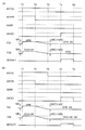
- the figure explaining the circuit which determines difference data. 6 is a timing chart for explaining the operation of a circuit for determining difference data.
- the figure explaining the circuit which determines difference data. 6 is a timing chart for explaining the operation of a circuit for determining difference data.
- the figure explaining the circuit which determines difference data. 6 is a timing chart for explaining the operation of a circuit for determining difference data.
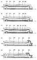
- FIG. 10 is a circuit diagram illustrating a pixel. 6 is a timing chart illustrating operation of a pixel. 6 is a timing chart illustrating operation of a pixel.
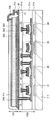
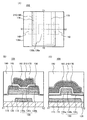
- FIG. 14 is a cross-sectional view illustrating a structure of an imaging device. Sectional drawing explaining the connection form of a photoelectric conversion element. Sectional drawing explaining the connection form of a photoelectric conversion element.
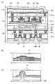
- FIG. 14 is a cross-sectional view illustrating a structure of an imaging device. Sectional drawing explaining the connection form of a photoelectric conversion element. Sectional drawing explaining the structure of an imaging device.
- FIG. 14 is a cross-sectional view illustrating a structure of an imaging device. Sectional drawing explaining the structure of an imaging device.
- FIG. 14 is a cross-sectional view illustrating a structure of an imaging device.
- FIG. 14 is a cross-sectional view illustrating a structure of an imaging device.
- FIG. 14 is a cross-sectional view illustrating a structure of an imaging device.
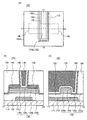
- 4A and 4B are a top view and cross-sectional views illustrating a transistor.
- 4A and 4B are a top view and cross-sectional views illustrating a transistor.
- 4A and 4B are a top view and cross-sectional views illustrating a transistor.
- 4A and 4B are a top view and cross-sectional views illustrating a transistor.
- 4A and 4B are a top view and cross-sectional views illustrating a transistor.
- 4A and 4B are a top view and cross-sectional views illustrating a transistor.
- 4A and 4B are a top view and cross-sectional views illustrating a transistor.
- 4A and 4B are a top view and cross-sectional views illustrating a transistor.
- FIG. 6A and 6B illustrate a range of the atomic ratio of an oxide semiconductor.
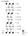
- FIG. 6 illustrates a crystal of InMZnO 4 .
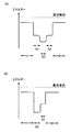
- FIG. 11 is a band diagram of a stacked structure of an oxide semiconductor.
- 10A and 10B each illustrate an electronic device.
- 6 is a flowchart illustrating an operation method of the imaging device.
- X and Y are assumed to be objects (for example, devices, elements, circuits, wirings, electrodes, terminals, conductive films, layers, etc.).
- an element that enables electrical connection between X and Y for example, a switch, a transistor, a capacitor, an inductor, a resistor, a diode, a display, etc.
- Element, light emitting element, load, etc. are not connected between X and Y
- elements for example, switches, transistors, capacitive elements, inductors
- resistor element for example, a diode, a display element, a light emitting element, a load, or the like.
- an element for example, a switch, a transistor, a capacitive element, an inductor, a resistance element, a diode, a display, etc.
- the switch has a function of controlling on / off. That is, the switch is in a conductive state (on state) or a non-conductive state (off state), and has a function of controlling whether or not to pass a current. Alternatively, the switch has a function of selecting and switching a path through which a current flows.
- the case where X and Y are electrically connected includes the case where X and Y are directly connected.
- a circuit for example, a logic circuit (an inverter, a NAND circuit, a NOR circuit, etc.) that enables a functional connection between X and Y, signal conversion, etc.
- a circuit for example, a logic circuit (an inverter, a NAND circuit, a NOR circuit, etc.) that enables a functional connection between X and Y, signal conversion, etc.
- Circuit (D / A conversion circuit, A / D conversion circuit, gamma correction circuit, etc.), potential level conversion circuit (power supply circuit (boost circuit, step-down circuit, etc.), level shifter circuit that changes signal potential level, etc.), voltage source, Current source, switching circuit, amplifier circuit (circuit that can increase signal amplitude or current amount, operational amplifier, differential amplifier circuit, source follower circuit, buffer circuit, etc.), signal generation circuit, storage circuit, control circuit, etc.)
- One or more can be connected between Y and Y.
- Y and Y One or more can be connected between Y and Y.
- X and Y are functionally connected.
- the case where X and Y are functionally connected includes the case where X and Y are directly connected and the case where X and Y are electrically connected.
- the source (or the first terminal) of the transistor is electrically connected to X through (or not through) Z1, and the drain (or the second terminal or the like) of the transistor is connected to Z2.
- Y is electrically connected, or the source (or the first terminal, etc.) of the transistor is directly connected to a part of Z1, and another part of Z1 Is directly connected to X, the drain (or second terminal, etc.) of the transistor is directly connected to a part of Z2, and another part of Z2 is directly connected to Y.
- X and Y, and the source (or the first terminal or the like) of the transistor and the drain (or the second terminal or the like) are electrically connected to each other. Terminal, etc., the drain of the transistor (or the second terminal, etc.) and Y are electrically connected in this order. ” Or “the source (or the first terminal or the like) of the transistor is electrically connected to X, the drain (or the second terminal or the like) of the transistor is electrically connected to Y, and X or the source ( Alternatively, the first terminal and the like, the drain of the transistor (or the second terminal, and the like) and Y are electrically connected in this order.
- X is electrically connected to Y through the source (or the first terminal or the like) and the drain (or the second terminal or the like) of the transistor, and X is the source of the transistor (or the first terminal or the first terminal). Terminal, etc.), the drain of the transistor (or the second terminal, etc.), and Y are provided in this connection order.
- Terminal, etc.), the drain of the transistor (or the second terminal, etc.), and Y are provided in this connection order.
- a source (or a first terminal or the like of a transistor) is electrically connected to X through at least a first connection path, and the first connection path is The second connection path does not have a second connection path, and the second connection path includes a transistor source (or first terminal or the like) and a transistor drain (or second terminal or the like) through the transistor.
- the first connection path is a path through Z1
- the drain (or the second terminal, etc.) of the transistor is electrically connected to Y through at least the third connection path.
- the third connection path is connected and does not have the second connection path, and the third connection path is a path through Z2.
- the source of the transistor (or the first terminal or the like) is electrically connected to X via Z1 by at least a first connection path, and the first connection path is a second connection path.
- the second connection path has a connection path through a transistor, and the drain (or the second terminal or the like) of the transistor is at least connected to Z2 by the third connection path.
- Y, and the third connection path does not have the second connection path.
- the source of the transistor (or the first terminal or the like) is electrically connected to X through Z1 by at least a first electrical path, and the first electrical path is a second electrical path Does not have an electrical path, and the second electrical path is an electrical path from the source (or first terminal or the like) of the transistor to the drain (or second terminal or the like) of the transistor;
- the drain (or the second terminal or the like) of the transistor is electrically connected to Y through Z2 by at least a third electrical path, and the third electrical path is a fourth electrical path.
- the fourth electrical path is an electrical path from the drain (or second terminal or the like) of the transistor to the source (or first terminal or the like) of the transistor.
- Can By defining the connection path in the circuit configuration using the same expression method as in these examples, the source (or the first terminal, etc.) and the drain (or the second terminal, etc.) of the transistor are distinguished from each other. The technical scope can be determined.
- X, Y, Z1, and Z2 are objects (for example, devices, elements, circuits, wirings, electrodes, terminals, conductive films, layers, and the like).
- the term “electrically connected” in this specification includes in its category such a case where one conductive film has functions of a plurality of components.
- film and “layer” can be interchanged with each other depending on the case or circumstances.
- conductive layer may be changed to the term “conductive film”.
- insulating film may be changed to the term “insulating layer” in some cases.
- the potential is relative, and the magnitude is determined by the relative magnitude from the reference potential. Therefore, even when “ground”, “GND”, “ground”, and the like are described, the potential is not necessarily 0 volts.
- “ground” or “GND” may be defined with reference to the lowest potential in the circuit.
- “ground” or “GND” may be defined with reference to an intermediate potential in the circuit. In that case, a positive potential and a negative potential are defined based on the potential.
- One embodiment of the present invention is a configuration and an operation method of an imaging device including a circuit that determines whether there is a significant difference between two different frames.
- the imaging apparatus includes a pixel that can output difference data, a circuit that determines the difference data, a circuit that controls power supply, an A / D converter, and the like.
- the presence / absence of a significant difference can be determined at high speed. If it is determined that there is no difference, the power supply to the A / D converter or the like can be cut off to reduce power consumption.
- a transistor using an oxide semiconductor as an active layer (hereinafter referred to as an OS transistor) is preferably used for the pixel circuit. Since the OS transistor has a small off-state current, a memory for holding data in the pixel circuit can be easily configured.
- FIG. 1 is a block diagram of an imaging device of one embodiment of the present invention.
- the imaging apparatus includes a pixel array 21, a circuit 22, a circuit 23, a circuit 24, a circuit 25, and a circuit 26.
- the pixel array 21 has pixels 20.
- the pixels 20 can be arranged in a matrix of, for example, m rows and n columns (m and n are natural numbers of 1 or more).
- the pixel 20 can output image data or difference data of two different frames to the electrically connected wiring 91 (OUT1).
- One circuit 22 is provided for each column, and is electrically connected to the wiring 91 (OUT1).
- the circuit 22 can have a function of determining the significance of difference data output from the pixel 20. Note that the difference data is significant means that the difference data is greater than or equal to a value that can be determined to have a difference. The value can be arbitrarily set by the practitioner.
- the circuit 22 when it is determined that the difference data has no difference, the circuit 22 outputs a low level potential (hereinafter, “L”) to the wiring 92 (OUT2). When the difference data is determined to have a difference, the circuit 22 outputs a high level potential (hereinafter, “H”) to the wiring 92 (OUT2). Note that the logic of the signal output as the determination result of the presence or absence of the difference may be reversed.
- the circuit 23 can have a function as a row driver that selects the pixels 20 for each row. Image data or difference data is output from the pixel 20 selected by the circuit 23 to the wiring 91 (OUT1).
- a shift register or the like can be used for the circuit 23, for example, a shift register or the like can be used.
- the circuit 24 is electrically connected to the wiring 91 (OUT1).
- the circuit 24 can have a function of converting image data of an analog signal output from the pixel 20 into a digital signal.
- an A / D converter or the like can be used for the circuit 24.
- the circuit 24 can be provided for each column.
- the circuit 25 can have a function as a column driver that sequentially selects the circuit 24 provided for each column. A digital signal corresponding to image data is output from the circuit 24 selected by the circuit 25 to the wiring 93 (OUT3).
- a shift register or the like can be used as the circuit 25, for example.
- the circuit 26 is electrically connected to peripheral circuits such as the circuit 24 and the circuit 25 and the wiring 92 (OUT2).
- the circuit 26 can have a function of controlling power supply to the circuit 24 and the circuit 25 in accordance with a signal potential input from the wiring 92 (OUT2).
- the imaging apparatus acquires new image data and performs an operation of rewriting or recording the output destination image data. Do. Therefore, when it is determined that there is a difference, the circuit 26 performs control to continue or restart the power supply to the circuit 24 and the circuit 25, and reads image data from the pixel 20.
- circuit 26 only needs to have a function of controlling power supply to the circuit 24, the circuit 25, and the like in accordance with the potential of the wiring 92 (OUT2). Therefore, other circuits may have the function of the circuit 26. Alternatively, the circuit 26 may be omitted, and the operation related to the function may be performed using software.
- the imaging device of one embodiment of the present invention may have a structure illustrated in FIG.
- the imaging apparatus is different from the imaging apparatus shown in FIG.
- the circuit 27 is provided for each row and is electrically connected to the wiring 90 (RDSE).
- the circuit 27 is electrically connected to the row wiring that connects the circuit 23 and the pixel 20.
- the circuit 27 can have a function of controlling electrical connection between the circuit 23 and the pixel 20. Further, the circuit 27 can select all the pixels 20 included in the pixel array 21.
- FIG. 2B illustrates an example of a specific structure of the circuit 27, which includes a p-ch transistor and an n-ch transistor.
- One of the source and the drain of the p-ch transistor is electrically connected to the circuit 23, and the other of the source and the drain is electrically connected to the pixel 20.
- One of a source and a drain of the n-ch transistor is electrically connected to a high potential power supply line (VDD), and the other of the source and the drain is electrically connected to the pixel 20.
- VDD high potential power supply line
- Each gate of the p-ch transistor and the n-ch transistor is electrically connected to the wiring 90 (RDSE).
- the circuit 27 can select whether or not the circuit 23 is used depending on a signal potential input from the wiring 90 (RDSE).
- the p-ch transistor When the potential of the wiring 90 (RDSE) is “L”, the p-ch transistor is turned on, the n-ch transistor is turned off, and the circuit 23 and the pixel 20 are turned on. That is, the operation mode using the circuit 23 is set, and the same operation as that of the imaging apparatus shown in FIG. 1 can be performed.
- the p-ch transistor When the potential of the wiring 90 (RDSE) is “H”, the p-ch transistor is turned off, and the circuit 23 and the pixel 20 are turned off. That is, an operation mode in which the circuit 23 is not used can be set. Further, the n-ch transistor is turned on, and “H” is supplied to all the pixels 20 from the high potential power supply line (VDD). That is, all the pixels 20 are selected. Note that as another configuration of the circuit 27, an OR circuit using the output signal of the circuit 23 and the signal of the wiring 90 as an input signal and a signal to the pixel 20 as an output signal can be used.
- one column of pixels 20 is electrically connected to one wiring 91 (OUT1), if a significant difference potential can be output from any of the pixels 20 in the column direction when the difference data is acquired.
- the circuit 22 can determine that there is a difference.
- each circuit 22 provided for each column uses the wiring 92 (OUT2) as a common output line, if any circuit 22 determines that there is a difference, the potential of the wiring 92 (OUT2) is “ H ”. In other words, it is possible to determine whether or not there is a difference substantially simultaneously for all the pixels 20.
- the circuit 26 controls power supply to the circuit 23 in addition to the circuit 24 and the circuit 25 by the signal potential input from the wiring 92 (OUT2). Also good.
- the circuit 26 When the signal potential is “L”, that is, when the circuit 22 determines that there is no difference, the circuit 26 performs control to cut off the power supply to the circuit 23, the circuit 24, and the circuit 25.
- the signal potential is “H”, that is, when the circuit 22 determines that there is a difference, the circuit 26 performs control to continue or restart the power supply to the circuit 23, the circuit 24, and the circuit 25.
- the wiring 90 can be electrically connected to the wiring 91 (OUT1) if the circuit 27 appropriately operates in accordance with the logic signal output from the circuit 22.
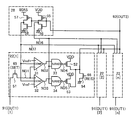
- FIG. 3 shows an example of the configuration of the circuit 22.
- the circuit 22 [1] and the wiring 91 (OUT1) [1] mean the circuit 22 and the wiring 91 (OUT1) provided in the first column. 3 illustrates the configuration in which the circuits 22 are provided for all the wirings 91 (OUT1), the circuits 22 may be provided for every several columns, every several tens of columns, or every several hundred columns. That is, there may be a column that does not detect difference data.
- the circuit 22 can include a transistor 51, a transistor 52, a transistor 53, a transistor 54, a comparator circuit 31, and a comparator circuit 32.
- the polarity of the transistors 51 and 54 is n-ch type
- the polarity of the transistors 52 and 53 is p-ch type.
- the polarity of the transistors can be changed by changing the operating conditions.
- One of a source and a drain of the transistor 51 is electrically connected to the wiring 91 (OUT1).
- the other of the source and the drain of the transistor 51 is electrically connected to one input terminal of the comparator circuit 31.
- the other of the source and the drain of the transistor 51 is electrically connected to the other input terminal of the comparator circuit 32.
- the output terminal of the comparator circuit 31 is electrically connected to the gate of the transistor 52.
- the output terminal of the comparator circuit 32 is electrically connected to the gate of the transistor 53.
- One of the source and the drain of the transistor 52 is electrically connected to one of the source and the drain of the transistor 54.
- One of the source and the drain of the transistor 53 is electrically connected to one of the source and the drain of the transistor 54.
- One of a source and a drain of the transistor 54 is electrically connected to the wiring 92 (OUT2).
- the other input terminal of the comparator circuit 31 is supplied with either the upper limit or the lower limit (for example, Vref ⁇ ) of the voltage for determining the significance of the difference data.
- One input terminal of the comparator circuit 32 is supplied with the other of the upper limit and the lower limit of the voltage for determining the significance of the difference data (for example, Vref +).
- a high potential eg, VDD
- a low potential eg, GND
- GND is supplied to the other of the source and the drain of the transistor 54.
- the gate of the transistor 51 is electrically connected to the wiring 65 (SET).
- the gate of the transistor 54 is electrically connected to the wiring 66 (RES).
- the wiring 65 (SET) and the wiring 66 (RES) can function as signal lines for controlling conduction of transistors connected to the wiring 65 (SET) and the wiring 66 (RES).
- a constant high potential power supply (BIAS) capable of controlling the circuit operation is supplied to the power supply input terminals of the comparator circuits 31 and 32.
- a wiring to which the other of the source and the drain of the transistor 51, one input terminal of the comparator circuit 31, and the other input terminal of the comparator circuit 32 are connected is referred to as a node ND1.
- a wiring to which the output terminal of the comparator circuit 31 and the gate of the transistor 52 are connected is referred to as a node ND2.
- a wiring to which the output terminal of the comparator circuit 32 and the gate of the transistor 53 are connected is referred to as a node ND3.
- the difference data output from the pixel 20 can be input to the comparator circuits 31 and 32.
- the comparator circuits 31 and 32 an upper limit or a lower limit of a voltage for determining the significance of the difference data is set, and the circuit 22 can output signals having different logics depending on the presence or absence of the difference.
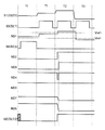
- a period T0 is a reset operation period in which the potential of the wiring 92 (OUT2) is set to “L”.
- the potential of the wiring 92 (OUT2) is reset to “L”.
- the period T1 illustrates an operation when the difference data output from the pixel 20 is within the upper and lower limit values set in the comparator circuits 31 and 32, that is, when it is determined that there is no difference.
- the period T2 illustrates the operation when the difference data output from the pixel 20 exceeds the upper limit set in the comparator circuit 31, that is, when it is determined that there is a difference.
- the period T3 illustrates the operation when the difference data output from the pixel 20 is below the lower limit set in the comparator circuit 32, that is, when it is determined that there is a difference.
- the difference determination operation exemplified in the period T ⁇ b> 1 or the like may be performed in accordance with the row selection operation by the circuit 23. That is, the determination operation for the maximum number of rows is performed in one frame period. Note that by controlling the potential of the wiring 65 (SET), a difference determination operation can be performed every several rows, every several tens of rows, or every several hundred rows. In addition, the difference determination operation can be intensively performed in a partial region of the pixel array 21, for example, only in a row near the center.
- FIG. 5 shows an example of the configuration of the circuit 22 different from that in FIG.
- FIG. 3 illustrates the configuration in which the circuits 22 are provided in all the wirings 91 (OUT1)
- the circuits 22 may be provided every several columns, every several tens of columns, or every several hundred columns.
- the circuit 22 is electrically connected to the circuit 28.
- the circuit 22 illustrated in FIG. 5 can include a transistor 51, a transistor 52, a transistor 53, a transistor 54, a comparator circuit 31, a comparator circuit 32, a NAND circuit 33, and a NAND circuit 34.
- the polarity of the transistors 51 and 54 is n-ch type
- the polarity of the transistors 52 and 53 is p-ch type.
- the polarity of the transistors can be changed by changing the operating conditions.
- One of a source and a drain of the transistor 51 is electrically connected to the wiring 91 (OUT1).
- the other of the source and the drain of the transistor 51 is electrically connected to one input terminal of the comparator circuit 31.
- the other of the source and the drain of the transistor 51 is electrically connected to the other input terminal of the comparator circuit 32.
- the output terminal of the comparator circuit 31 is electrically connected to one input terminal of the NAND circuit 33.
- the output terminal of the comparator circuit 32 is electrically connected to one input terminal of the NAND circuit 34.
- the output terminal of the NAND circuit 33 is electrically connected to the gate of the transistor 52.
- the output terminal of the NAND circuit 34 is electrically connected to the gate of the transistor 53.
- One of the source and the drain of the transistor 52 is electrically connected to one of the source and the drain of the transistor 54.
- One of the source and the drain of the transistor 53 is electrically connected to one of the source and the drain of the transistor 54.
- One of a source and a drain of the transistor 54 is electrically connected to the wiring 92 (OUT2).
- the other input terminal of the comparator circuit 31 is supplied with either the upper limit or the lower limit of the voltage for determining the significance of the difference data (for example, Vref +).
- One input terminal of the comparator circuit 32 is supplied with the other of the upper limit and the lower limit of the voltage for determining the significance of the difference data (for example, Vref ⁇ ).
- a high potential eg, VDD
- a low potential eg, GND
- the comparator circuits 31 and 32 are supplied with a constant high potential power supply (BIAS) or a low potential (for example, GND) capable of controlling the circuit operation via the circuit 28.
- a high potential (for example, VDD) or a low potential (for example, GND) is supplied to the other input terminals of the NAND circuits 33 and 34 via the circuit 28.
- a wiring to which the other of the source and the drain of the transistor 51, one input terminal of the comparator circuit 31, and the other input terminal of the comparator circuit 32 are connected is referred to as a node ND1.
- a wiring to which the output terminal of the comparator circuit 31 and one input terminal of the NAND circuit 33 are connected is referred to as a node ND2.
- a wiring to which the output terminal of the comparator circuit 32 and one input terminal of the NAND circuit 34 are connected is referred to as a node ND3.
- a wiring to which the output terminal of the NAND circuit 33 and the gate of the transistor 52 are connected is referred to as a node ND4.
- a wiring to which the output terminal of the NAND circuit 34 and the gate of the transistor 53 are connected is referred to as a node ND5.
- the circuit 28 can include a transistor 55, a transistor 56, a transistor 57, and a transistor 58.
- the polarity of the transistors 55 and 57 is p-ch type, and the polarity of the transistors 56 and 57 is n-ch type.
- the polarity of the transistors can be changed by changing the operating conditions.
- One of the source and the drain of the transistor 55 is electrically connected to one of the source and the drain of the transistor 56.
- One of the source and the drain of the transistor 55 is electrically connected to the other input terminal of the NAND circuits 33 and 34.
- a wiring to which one of the source and the drain of the transistor 55, one of the source and the drain of the transistor 56, and the other input terminal of the NAND circuits 33 and 34 are connected is referred to as a node ND6.
- One of a source and a drain of the transistor 57 is electrically connected to one of a source and a drain of the transistor 58.
- One of the source and the drain of the transistor 57 is electrically connected to the power input terminals of the comparator circuits 31 and 32.
- a wiring to which one of the source and the drain of the transistor 57, one of the source and the drain of the transistor 58, and the power supply input terminals of the comparator circuits 31 and 32 are connected is referred to as a node ND7.
- Gates of the transistors 55 to 58 are electrically connected to the wiring 92 (OUT2).
- a high potential eg, VDD
- the other of the source and the drain of the transistor 57 is supplied with a constant high potential power supply (BIAS) capable of controlling the circuit operation of the comparator circuits 31 and 32.
- a low potential for example, GND is supplied to the other of the source and the drain of the transistors 54 and 58.
- the circuit 22 inputs a potential output to the wiring 92 (OUT2) to the circuit 28.
- the circuit 28 can stop some of the circuits included in the circuit 22 in accordance with the value of the potential. Therefore, power consumption can be reduced.
- the GND potential is supplied to the comparator circuits 31 and 32, and the circuit becomes inoperative. Further, “L” is supplied to the other input terminals of the NAND circuits 33 and 34, and the potentials of the nodes ND4 and ND5 are fixed to “H”. Therefore, since the potential of the wiring 92 (OUT2) is fixed to “H”, unnecessary difference detection operation is not performed for the remaining period until one frame is completed, and power consumption can be suppressed.
- a period T0 is a reset operation period in which the potential of the wiring 92 (OUT2) is set to “L”.
- the potential of the wiring 92 (OUT2) is reset to “L”.
- BIAS is supplied to the comparator circuits 31 and 32, and “H” is supplied to the other input terminals of the NAND circuits 33 and 34.
- the period T1 illustrates an operation when the difference data output from the pixel 20 is within the upper and lower limit values set in the comparator circuits 31 and 32, that is, when it is determined that there is no difference.
- the period T2 illustrates the operation when the difference data output from the pixel 20 exceeds the upper limit set in the comparator circuit 31, that is, when it is determined that there is a difference.
- the potential of the wiring 92 (OUT2) is “H”
- the potential of the node ND6 is “L”. Therefore, the potential of the node ND4 increases from “L” to “H”.
- the period T3 illustrates the operation when the difference data output from the pixel 20 is below the lower limit set in the comparator circuit 32, that is, when it is determined that there is a difference.
- the potentials of the nodes ND2 to ND5 are fixed in the period T2
- the potential of the wiring 92 (OUT2) is “H” regardless of the potential of the node ND1. Accordingly, in the circuit, the period T3 does not change from the state of the period T2.
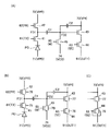
- the circuit 28 shown in FIG. 5 can be replaced with the circuit 29 shown in FIG.
- the circuit 29 can include a NOR circuit 35, an inverter circuit 36, a level shifter circuit 37, a transistor 59, and a transistor 60.
- the polarity of the transistors 59 and 60 is an n-ch type, but the polarity of the transistors can be changed by changing the operating conditions.
- One input terminal of the NOR circuit is electrically connected to the wiring 92 (OUT2).
- the output terminal of the NOR circuit is electrically connected to the inverter circuit 36, the gate of the transistor 59, and the inverting input terminal of the level shifter circuit 37.
- the output terminal of the inverter circuit 36 is electrically connected to the input terminal of the level shifter circuit 37.
- the output terminal of the level shifter circuit 37 is electrically connected to the gate of the transistor 60.
- One of the source and the drain of the transistor 59 is electrically connected to one of the source and the drain of the transistor 60.
- a constant high potential power supply (BIAS) capable of controlling the circuit operation of the comparator circuits 31 and 32 is supplied to the other of the source and the drain of the transistor 59.
- the other of the source and the drain of the transistor 60 is supplied with a constant low potential power supply (AVSS) capable of controlling the circuit operation of the comparator circuits 31 and 32.
- AVSS constant low potential power supply
- the wiring 94 is connected to the other input terminal of the NOR circuit 35, and an operation signal (AENE) is input thereto.
- a wiring to which the output terminal of the NOR circuit is electrically connected is connected to the NAND circuits 33 and 34 and corresponds to the node ND6 in FIG.
- a wiring electrically connected to one of the source and the drain of the transistor 59 is connected to the comparator circuits 31 and 32 and corresponds to the node ND7 in FIG.
- the low level potential “L” input to the power input terminals of the comparator circuits 31 and 32 can be made appropriate.
- the power supply voltage of the comparator circuits 31 and 32 (analog circuit) and the power supply voltage of other circuits (digital circuit) are not distinguished.
- the analog circuit may not be stopped normally at the low level potential “L” supplied from the circuit 28. Therefore, it is preferable to set the voltage value of the low level potential “L” in accordance with the operation of the analog circuit.
- AVSS can be supplied as the low level potential “L” of the comparator circuits 31 and 32.
- the circuit 29 when the operation signal (AENE) is input from the wiring 94, the potentials of the nodes ND6 and ND7 can be set to "L" regardless of the potential of the wiring 91 (OUT1).
- the circuit 29 can be selected and operated. For example, if each of the wirings that can individually supply the operation signal (AENE) and the circuit 29 are configured so that one circuit 29 controls half of the circuits 22, all the circuits 22 are operated. In addition, half of the circuits 22 can be operated and half of the circuits 22 can be stopped. Therefore, power consumption can be reduced.
- the number of operations of the circuit 22 can be controlled more finely.
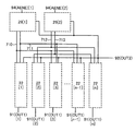
- the wiring 94 [1] and the wiring 94 [2] to which the operation signal (AENE) can be individually supplied, the circuit 29 [1] to which the wiring 94 [1] is connected, and the wiring 94 [2] are connected.
- the circuits 22 [4] to 22 [n-2] (not shown) are connected to either the circuit 29 [1] or the circuit 29 [2].
- the circuits 22 [1] to [n] are connected to the circuits 29 [1] and [2] through the wiring 92 (OUT2).
- wirings 710 and 712 correspond to the node ND6 illustrated in FIG.
- the wirings 711 and 713 correspond to the node ND7 shown in FIG.
- FIG. 9 is a timing chart for explaining the operation of the circuit shown in FIG.
- an operation when the potential of the wiring 94 [1] is “H” and the potential of the wiring 94 [2] is “L” is described.
- the operation of the circuit 22 in the periods T0 to T3 is the same as that described in the timing chart in FIG.
- the voltage at which the output of the circuit 22 is fixed is supplied from the circuit 29 [2] to which the wiring 94 [2] is connected regardless of the input signal and the output signal to the circuit 22. Therefore, the circuit 22 [2], the circuit 22 [n], and the like connected to the circuit 29 [2] via the wirings 712 and 713 do not perform the difference data determination operation. That is, in the circuit shown in FIG. 9, the difference determination operation can be performed without operating half of the circuits.
- the imaging apparatus can select and execute a first imaging mode for acquiring image data or a second imaging mode for acquiring difference data between two different frames.
- an image mode is acquired in the first imaging mode (S1).
- the image data (analog data) is output from the pixel 20 for each row selected by the circuit 23 to the circuit 24 and converted into digital data.
- the circuit 25 sequentially selects columns and outputs the digital data to the outside (S2). The above operation is repeated from the first line to the last line within one frame period.
- the mode is switched to the second imaging mode (S3).
- Difference data is acquired in the second imaging mode and output from the pixel 20 to the circuit 22 (S4).
- the circuit 22 determines the significance of the difference data (S5).
- the signal potential “L” is output to the circuit 26 (S8), and the power supply to the circuit 24 and the circuit 25 is cut off (S7). Then, the process returns to S4 to acquire difference data again.
- the circuit 26 performs control to resume power supply to the circuit 24 and the circuit 25.
- the circuit 23 may be included as a target of a circuit for which the circuit 26 controls power supply.
- an imaging device with low power consumption can be provided.
- Embodiment 2 In this embodiment, an example of a pixel circuit applicable to the pixel 20 included in the imaging device described in Embodiment 1 and a driving method thereof will be described.
- FIG. 10A illustrates an example of a pixel circuit that can be used as the pixel 20. Note that FIG. 10A illustrates an example in which transistors are n-ch transistors; however, one embodiment of the present invention is not limited thereto, and some transistors are replaced with p-ch transistors. Also good.
- the pixel circuit can include a photoelectric conversion element PD, a transistor 41, a transistor 42, a transistor 43, a transistor 44, a transistor 45, a capacitor C1, and a capacitor C2. Note that the capacitor C2 may not be provided.
- One terminal of the photoelectric conversion element PD is electrically connected to one of the source and the drain of the transistor 41.
- the other of the source and the drain of the transistor 41 is electrically connected to one of the source and the drain of the transistor 42.
- the other of the source and the drain of the transistor 41 is electrically connected to one terminal of the capacitor C1.
- the other terminal of the capacitor C ⁇ b> 1 is electrically connected to one of the source and the drain of the transistor 45.
- the other terminal of the capacitor C ⁇ b> 1 is electrically connected to the gate of the transistor 43.
- the other terminal of the capacitive element C1 is electrically connected to one terminal of the capacitive element C2.
- One of the source and the drain of the transistor 43 is electrically connected to one of the source and the drain of the transistor 44.
- the other terminal of the capacitor C ⁇ b> 2 is electrically connected to the other of the source and the drain of the transistor 43.
- a node to which one of the source and the drain of the transistor 41, one of the source and the drain of the transistor 42, and one terminal of the capacitor C1 are connected is FD1. Further, a node to which the other terminal of the capacitor C1, one of the source and the drain of the transistor 45, the gate of the transistor 43, and one terminal of the capacitor C2 are connected is FD2.
- the other terminal of the photoelectric conversion element PD is electrically connected to the wiring 71 (VPD).
- the other of the source and the drain of the transistor 42 is electrically connected to the wiring 72 (VPR).
- the other of the source and the drain of the transistor 45 is electrically connected to the wiring 74 (VCS).
- the other of the source and the drain of the transistor 43 and the other terminal of the capacitor C2 are electrically connected to the wiring 73 (VPI).
- the other of the source and the drain of the transistor 44 is electrically connected to the wiring 91 (OUT1).
- the wiring 71 (VPD), the wiring 72 (VPR), the wiring 73 (VPI), and the wiring 74 (VCS) can function as power supply lines.
- the wiring 71 (VPD) and the wiring 74 (VCS) can function as low potential power supply lines.
- the wiring 72 (VPR) and the wiring 73 (VPI) can function as high potential power supply lines.
- a gate of the transistor 41 is electrically connected to the wiring 61 (TX).
- a gate electrode of the transistor 42 is electrically connected to the wiring 62 (PR).
- a gate of the transistor 45 is electrically connected to the wiring 63 (W).
- a gate of the transistor 44 is electrically connected to the wiring 63 (SE).
- the wiring 61 (TX), the wiring 62 (PR), the wiring 63 (SE), and the wiring 65 (W) can function as signal lines that control conduction of the transistors.
- the other terminal of the capacitor C2 may be connected not to the wiring 73 (VPI) but to other wiring or the like that can supply a fixed potential.
- the transistor included in the pixel circuit may be provided with a back gate as illustrated in FIG.
- FIG. 10B illustrates a structure in which a constant potential is applied to the back gate, and the threshold voltage can be controlled.
- Different potentials can be individually supplied to the wirings 75 to 79 connected to the respective back gates. Note that a wiring connected to the back gate of the transistor 43 and the transistor 44 may be electrically connected.
- the threshold voltage shifts in the positive direction when a potential lower than the source potential is applied to the back gate. Conversely, when a potential higher than the source potential is applied to the back gate, the threshold voltage shifts in the negative direction. Therefore, when on / off of each transistor is controlled with a predetermined gate voltage, the off-state current can be reduced by applying a potential lower than the source potential to the back gate. In addition, when a potential higher than the source potential is applied to the back gate, the on-state current can be reduced.
- transistors with low off-state current are preferably used as the transistors 41, 42, and 45.
- OS transistors are preferably used as the transistors 41, 42, and 45.
- the transistors 43 and 44 function as amplification transistors, it is preferable to use transistors with high on-state current. By applying a potential higher than the source potential to the back gates of the transistors 43 and 44, the on-state current can be further increased. Accordingly, the read potential output to the wiring 91 (OUT1) can be quickly determined, that is, the operation can be performed at a high frequency.
- the transistors 43 and 44 are preferably transistors using silicon in the active region or active layer (hereinafter referred to as Si transistors).
- the transistor 44 may have a structure in which the same potential as that of the front gate is applied to the back gate as illustrated in FIG.
- the transistors 43 and 44 may be OS transistors instead of Si transistors. Although the on-state current of the OS transistor is relatively small, the on-state current can be increased by providing the back gate, and the OS transistor can be operated at a high frequency.
- a plurality of potentials such as a signal potential and a potential applied to the back gate are used inside the imaging device.
- a plurality of potentials are supplied from the outside of the imaging device, the number of terminals and the like increase. Therefore, it is preferable to have a power supply circuit that generates a plurality of potentials inside the imaging device.
- the OS transistor Since the OS transistor has extremely low off-state current characteristics, the periods during which charges can be held at the nodes FD1 and FD2 can be extremely long due to the low off-state current characteristics of the transistors 41, 42, and 443. Therefore, it is possible to apply a global shutter system in which charge accumulation operation is simultaneously performed in all pixels without complicating a circuit configuration and an operation method.
- the imaging device of one embodiment of the present invention can also be operated by a rolling shutter system.
- the OS transistor can be used in a very wide temperature range because the temperature dependence of the electrical characteristic variation is smaller than that of the Si transistor. Therefore, an imaging device and a semiconductor device having an OS transistor are suitable for mounting on automobiles, aircraft, spacecrafts, and the like.
- the OS transistor has a higher drain breakdown voltage than the Si transistor.
- a photoelectric conversion element using a selenium-based material as a photoelectric conversion layer it is preferable to operate by applying a relatively high voltage (for example, 10 V or more) in order to use avalanche multiplication. Therefore, by combining an OS transistor and a photoelectric conversion element using a selenium-based material as a photoelectric conversion layer, an imaging device with high reliability can be obtained.
- the pixel circuit described in this embodiment holds the difference data between the operation in the first imaging mode in which image data is acquired and the imaging data of the initial frame and the imaging data of the current frame. It is possible to perform an operation in the second imaging mode that outputs a corresponding signal. In the second operation, difference data can be output without performing comparison processing or the like in an external circuit. Therefore, the pixel circuit is preferably used in the imaging device described in Embodiment 1.
- the potential of the wiring 61 (TX) is set to “H”
- the potential of the wiring 62 (PR) is set to “H”
- the potential of the wiring 65 (W) is set to “H”.
- the potential of the node FD1 is set to the potential VPR of the wiring 72 (VPR)
- the potential of the node FD2 is set to the potential VCS of the wiring 74 (VCS) (reset operation).
- the potential of the wiring 61 (TX) is “H”
- the potential of the wiring 62 (PR) is “L”
- the potential of the wiring 65 (W) is “L”.
- the potential of the node FD1 decreases in accordance with the light applied to the photoelectric conversion element PD
- the potential of the node FD2 also decreases due to capacitive coupling.
- the reduced potential amount of the node FD1 at time T3 is VA
- the potential of the node FD1 is VPR ⁇ VA.
- the potential of the node FD2 decreases by VB and becomes VCS ⁇ VB (accumulation operation). Note that in the circuit configuration illustrated in FIG. 5A, the potential of the node FD1 and the node FD2 decreases as the light applied to the photoelectric conversion element PD increases.
- the potential of the wiring 61 (TX) is set to “H”
- the potential of the wiring 62 (PR) is set to “H”
- the potential of the wiring 65 (W) is set to “H”.
- the potential of the node FD1 is set to the potential VPR of the wiring 72 (VPR)
- the potential of the node FD2 is set to the potential VCS of the wiring 74 (VCS).
- the potential of the wiring 61 (TX) is “H”
- the potential of the wiring 62 (PR) is “L”
- the potential of the wiring 65 (W) is “H”.
- the potential of the node FD1 decreases in accordance with the light applied to the photoelectric conversion element PD.
- the reduced potential amount of the node FD1 at time T3 is VA
- the potential of the node FD1 is VPR ⁇ VA. Note that in the circuit configuration in FIG. 5A, the potential of the node FD1 decreases as the light applied to the photoelectric conversion element PD increases.
- the potential of the node FD1 is The potential of the node FD2 increases by VB due to capacitive coupling.
- VA and VB are potentials that reflect the illuminance of the first frame.
- the potential of the node FD1 is The potential of the node FD2 increases by VB due to capacitive coupling.
- VA and VB are potentials that reflect the illuminance of the first frame.
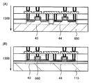
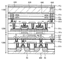
- FIG. 13 is a diagram illustrating an example of a specific configuration of the pixel 20, and is a cross-sectional view illustrating the channel length direction of the transistors 41, 42, 43, and 44 included in the pixel circuit.
- the wiring, the electrode, the metal layer, and the contact plug are illustrated as individual elements. However, when they are electrically connected, May be provided as the same element.
- the form in which elements such as wiring, electrodes, and metal layers are connected via the conductor 82 is merely an example, and each element may be directly connected without passing through the conductor 82.
- insulating layers 81 a to 81 k that function as protective films, interlayer insulating films, or planarization films are provided over the substrate and each element such as a transistor.
- an inorganic insulating film such as a silicon oxide film or a silicon oxynitride film can be used for the insulating layers 81a to 81k.
- an organic insulating film such as an acrylic resin or a polyimide resin may be used.
- the top surfaces of the insulating layers 81a to 81k and the like may be planarized by a CMP (Chemical Mechanical Polishing) method or the like as necessary.
- the pixel 20 can have a layer 1100 and a layer 1200.
- the layer 1100 can include the photoelectric conversion element PD.
- a two-terminal photodiode can be used for the photoelectric conversion element PD.
- the photodiode a pn-type photodiode using a single crystal silicon substrate, an amorphous silicon thin film, a pin-type photodiode using a microcrystalline silicon thin film or a polycrystalline silicon thin film, selenium or a compound of selenium, or an organic compound A photodiode using the above can be used.
- the photoelectric conversion element PD included in the layer 1100 is a pn photodiode using a single crystal silicon substrate.
- the photoelectric conversion element PD can include a p + region 620, a p ⁇ region 630, an n-type region 640, and a p + region 650.
- the layer 1200 can include an OS transistor included in the pixel circuit, and FIG. 13 illustrates the transistors 41, 42, 43, and 44 included in the pixel circuit.
- the photoelectric conversion element PD and the transistor can be overlapped with each other, and the light receiving area of the photoelectric conversion element PD can be widened.
- An insulating layer 80 is provided between the region where the OS transistor is formed and the region where the Si device (Si transistor or Si photodiode or the like) is formed.
- the insulating layer provided in the vicinity of the Si device preferably contains hydrogen in order to terminate dangling bonds of silicon.
- hydrogen in an insulating layer provided in the vicinity of an oxide semiconductor layer which is an active layer of the transistors 41 and 42 and the like is one of the factors that generate carriers in the oxide semiconductor layer. Therefore, the hydrogen may be a factor that decreases the reliability of the transistors 41 and 42 and the like. Therefore, in the case where one layer having a Si device and the other layer having an OS transistor are stacked, it is preferable to provide an insulating layer 80 having a function of preventing hydrogen diffusion therebetween. Since the insulating layer 80 can prevent hydrogen diffusion, the reliability of both the Si device and the OS transistor can be improved.
- the insulating layer 80 for example, aluminum oxide, aluminum oxynitride, gallium oxide, gallium oxynitride, yttrium oxide, yttrium oxynitride, hafnium oxide, hafnium oxynitride, yttria-stabilized zirconia (YSZ), or the like can be used.
- aluminum oxide, aluminum oxynitride, gallium oxide, gallium oxynitride, yttrium oxide, yttrium oxynitride, hafnium oxide, hafnium oxynitride, yttria-stabilized zirconia (YSZ), or the like can be used.
- One electrode (n-type region 640) of the photoelectric conversion element PD can be electrically connected to the transistor 41 through two conductors 82 and a wiring 69, for example.
- the conductor 82 since the conductor 82 is provided through the insulating layer 80, it is preferable that the conductor 82 also has a function of preventing hydrogen diffusion.
- the conductor 82 b that has a barrier property against hydrogen is formed on the outside in contact with at least the side wall of the through hole of the conductor 82, and the conductor 82 a having low resistance is formed on the inside.
- tungsten can be used for the conductor 82a
- tantalum nitride or the like can be used for the conductor 82b.
- the conductor 82 can also be comprised only with the conductor 82a. In the case where the conductor 82 does not contact the layer having an impurity such as hydrogen, the conductor 82 may be formed using only the conductor 82b.
- FIG. 13 illustrates a structure in which a top-gate OS transistor is provided in the layer 1200.
- the OS transistor is provided over a stack of insulating layers (insulating layers 81a, 80, and 81b) formed over the layer 1100, and includes an oxide semiconductor layer 130 and 140 and 150 that function as a source electrode and a drain electrode. And an insulating layer 160 functioning as a gate insulating layer and a conductive layer 170 functioning as a gate electrode. Note that the insulating layer 81b can also function as a gate insulating layer.
- FIG. 13 illustrates a structure in which the OS transistor is provided with a conductive layer 173 functioning as a back gate electrode.
- a structure in which a back gate electrode is provided also as a light-blocking layer is preferable. Further, by providing the back gate, the threshold voltage of the OS transistor can be controlled.
- the pixel 20 may have a stacked structure shown in FIG.
- a pixel 20 illustrated in FIG. 14 has a structure in which a layer 1200 and a layer 1100 are provided over a substrate 115. Since the photoelectric conversion element PD is provided over the OS transistor, electrical connection between the OS transistor and one electrode of the photoelectric conversion element PD is facilitated.
- FIG. 14 illustrates a mode in which a selenium-based material is used for the photoelectric conversion layer 561.
- a photoelectric conversion element PD using a selenium-based material has a high external quantum efficiency with respect to visible light. Further, since the selenium-based material has a high light absorption coefficient, it has an advantage that the photoelectric conversion layer 561 can be easily thinned.
- the photoelectric conversion element PD using a selenium-based material can be a highly sensitive sensor with large amplification by avalanche multiplication. That is, by using a selenium-based material for the photoelectric conversion layer 561, a sufficient photocurrent can be obtained even when the pixel area is reduced. Therefore, it can be said that the photoelectric conversion element PD using the selenium-based material is suitable for imaging in a low illumination environment.
- amorphous selenium or crystalline selenium can be used as the selenium-based material.
- Crystalline selenium can be obtained, for example, by heat-treating amorphous selenium after film formation. By making the crystal grain size of crystalline selenium smaller than the pixel pitch, it is possible to reduce variation in characteristics from pixel to pixel. Crystalline selenium has higher spectral sensitivity to visible light and higher light absorption coefficient than amorphous selenium.
- the photoelectric conversion layer 561 is illustrated as a single layer, but as shown in FIG. 15A, gallium oxide, cerium oxide, or In—Ga—Zn oxide is formed as a hole injection blocking layer 568 on the light receiving surface side. Things may be provided. Alternatively, as illustrated in FIG. 15B, nickel oxide, antimony sulfide, or the like may be provided as the electron injection blocking layer 569 on the electrode 566 side. Alternatively, as illustrated in FIG. 15C, a hole injection blocking layer 568 and an electron injection blocking layer 569 may be provided.
- the photoelectric conversion layer 561 may be a layer containing a compound of copper, indium, and selenium (CIS). Alternatively, it may be a layer containing a compound of copper, indium, gallium, and selenium (CIGS). In CIS and CIGS, a photoelectric conversion element using avalanche multiplication can be formed as in the case of a single layer of selenium.
- a photoelectric conversion element PD using a selenium-based material can have a structure in which a photoelectric conversion layer 561 is provided between an electrode 566 formed of a metal material or the like and a light-transmitting conductive layer 562, for example.
- CIS and CIGS are p-type semiconductors, and n-type semiconductors such as cadmium sulfide and zinc sulfide may be provided in contact with each other to form a junction.
- the light-transmitting conductive layer 562 and the wiring 71 are in direct contact with each other; however, the structure may be in which both are in contact with each other through the wiring 588 as illustrated in FIG.
- the photoelectric conversion layer 561 and the light-transmitting conductive layer 562 are not separated between pixel circuits, but may be separated between circuits as shown in FIG.
- FIG. 14 it is good also as a structure which does not provide the partition 567.
- the electrode 566, the wiring 71, and the like may be multilayer.
- the electrode 566 can have two layers of a conductive layer 566a and a conductive layer 566b
- the wiring 71 can have two layers of a conductive layer 71a and a conductive layer 71b.
- the conductive layer 566a and the conductive layer 71a are formed by selecting a low-resistance metal or the like, and the conductive layer 566a and the conductive layer 71a are metals having good contact characteristics with the photoelectric conversion layer 561. Or the like may be selected. With such a configuration, the electrical characteristics of the photoelectric conversion element PD can be improved.
- some metals may cause electrolytic corrosion when in contact with the light-transmitting conductive layer 562. Even when such a metal is used for the conductive layer 71a, electrolytic corrosion can be prevented through the conductive layer 71b.
- conductive layer 566b and the conductive layer 71b for example, molybdenum, tungsten, or the like can be used.
- conductive layer 566a and the conductive layer 71a for example, aluminum, titanium, or a stack in which aluminum is sandwiched between titanium can be used.
- the light-transmitting conductive layer 562 and the wiring 71 may be connected through a conductor 82 and a wiring 88.
- the partition wall 567 can be formed using an inorganic insulator, an insulating organic resin, or the like.
- the partition wall 567 may be colored black or the like in order to shield light from the transistor and / or to determine the area of the light receiving portion per pixel.
- the pixel 20 may have a stacked structure shown in FIG.
- the pixel 20 illustrated in FIG. 17 is different from the pixel 20 illustrated in FIG. 14 only in the layer 1100, and the other configurations are the same.
- the photoelectric conversion element PD included in the layer 1100 is a pin-type photodiode using an amorphous silicon film, a microcrystalline silicon film, or the like as the photoelectric conversion layer.
- the photoelectric conversion element PD can include an n-type semiconductor layer 565, an i-type semiconductor layer 564, a p-type semiconductor layer 563, an electrode 566, a wiring 71, and a wiring 588.
- the electrode 566 is electrically connected to the metal layer 405.
- the p-type semiconductor layer 563 is electrically connected to the wiring 71 through the wiring 588.
- Amorphous silicon is preferably used for the i-type semiconductor layer 564.
- amorphous silicon, microcrystalline silicon, or the like containing a dopant imparting each conductivity type can be used.
- a photodiode using amorphous silicon as a photoelectric conversion layer has high sensitivity in the wavelength region of visible light and can easily detect weak visible light.
- the configuration of the photoelectric conversion element PD having the form of a pin-type thin film photodiode and the connection form of the photoelectric conversion element PD and the wiring are examples shown in FIGS. 18A, 18B, and 18C. Also good.
- the configuration of the photoelectric conversion element PD and the connection form of the photoelectric conversion element PD and the wiring are not limited to these, and other forms may be used.
- FIG. 18A illustrates a structure in which a light-transmitting conductive layer 562 in contact with the p-type semiconductor layer 563 of the photoelectric conversion element PD is provided.
- the light-transmitting conductive layer 562 functions as an electrode and can increase the output current of the photoelectric conversion element PD.
- the light-transmitting conductive layer 562 can be formed using, for example, indium tin oxide, indium tin oxide containing silicon, indium oxide containing zinc, zinc oxide, zinc oxide containing gallium, zinc oxide containing aluminum, tin oxide, or fluorine. Tin oxide containing, tin oxide containing antimony, graphene, graphene oxide, or the like can be used.
- the light-transmitting conductive layer 562 is not limited to a single layer and may be a stack of different films.
- FIG. 18B illustrates a structure in which the light-transmitting conductive layer 562 and the wiring 71 are connected to each other through the conductor 82 and the wiring 588. Note that the p-type semiconductor layer 563 of the photoelectric conversion element PD and the wiring 71 may be connected to each other through the conductor 82 and the wiring 588. Note that in FIG. 18B, the light-transmitting conductive layer 562 can be omitted.
- FIG. 18C illustrates an opening in which the p-type semiconductor layer 563 is exposed in the insulating layer 81e that covers the photoelectric conversion element PD, and the light-transmitting conductive layer 562 and the wiring 71 that cover the opening are electrically connected. It is the structure which has a connection.
- the photoelectric conversion element PD formed using the above-described selenium-based material, amorphous silicon, or the like can be manufactured using a general semiconductor manufacturing process such as a film formation process, a lithography process, or an etching process.
- the selenium-based material has high resistance, and as illustrated in FIG. 14, the photoelectric conversion layer 561 can be configured not to be separated between circuits. Therefore, it can be manufactured at a low cost with a high yield.
- FIG. 19A is a cross-sectional view illustrating the channel length direction of the transistors 41, 42, 43, and 44.
- 19B is a cross-sectional view taken along dashed-dotted line X1-X2 in FIG. 19A and illustrates a cross section of the transistor 41 in the channel width direction.
- 19C is a cross-sectional view taken along dashed-dotted line Y1-Y2 in FIG. 19A and illustrates a cross section of the transistor 42 in the channel width direction.
- the layer 1100 can have a structure including the photoelectric conversion element PD similarly to the structure of the pixel 20 described above.
- FIG. 19A illustrates a configuration in which a selenium photoelectric conversion element PD is provided in the same manner as the configuration in FIG. 14, but a photoelectric transistor having a pin-type thin film photodiode similar to the configuration in FIG. 17 is illustrated.
- the structure provided with conversion element PD may be sufficient.
- the layer 1200 can include the transistors 41, 42, and 45.
- the transistor 45 is not shown.
- the layer 1300 can include the transistor 43 and the transistor 44.
- transistors 43 and 44 transistors using silicon as an active layer or an active region are preferably used.
- a transistor having silicon as an active layer or an active region has a large on-state current, and can efficiently amplify the potential of the node FD2.
- the capacitor C1 has a structure in which the conductive layer 84 and the conductive layer 85 are used as electrodes and the insulating layer 83 is used as a dielectric layer in the layer 1300, the capacitor C1 may be provided in the layer 1200. Further, although the capacitor C2 is not illustrated, the capacitor C2 may be provided in any of the layer 1200 and the layer 1300.
- the transistors 43 and 44 are illustrated as fin-type structures, but may be planar types as shown in FIG. Alternatively, as illustrated in FIG. 20B, a transistor including a silicon thin film active layer 660 may be used.
- the active layer 660 can be made of polycrystalline silicon or SOI (Silicon on Insulator) single crystal silicon.
- the photoelectric conversion element PD included in the layer 1100 may be a pn type photodiode using a single crystal silicon substrate as shown in FIG.
- the layer 1200 is formed over the layer 1300 and then the separately formed layer 1100 is attached.
- the layer 1200 is provided with an insulating layer 81i and metal layers 402a and 403a.
- the layer 1100 is provided with an insulating layer 81k and metal layers 402b and 403b.
- the metal layers 402a and 403a are provided to have a region embedded in the insulating layer 81h, and the metal layer 402a is electrically connected to one of the source and the drain of the transistor 41. Further, 403a is electrically connected to the wiring 71.
- the metal layers 402b and 403b are provided so as to have a region embedded in the insulating layer 81i, and the metal layer 402b is electrically connected to the n-type region 640 of the photoelectric conversion element PD. Further, 403b is electrically connected to the p + region 620 through the p + region 650.
- the metal layer 402a and the metal layer 402b, and the metal layer 403a and the metal layer 403b are provided at positions where they are in direct contact with each other, and have connection portions 402 and 403.
- the metal layer 402a and the metal layer 402b are preferably composed of the same metal element as a main component.
- the metal layer 403a and the metal layer 403b are preferably composed of the same metal element as a main component.
- the insulating layer 81i and the insulating layer 81k are preferably composed of the same component.
- Cu, Al, Sn, Zn, W, Ag, Pt, or Au can be used for the metal layers 402a, 402b, 403a, and 403b. From the viewpoint of ease of joining, Cu, Al, W, or Au is preferably used.
- silicon oxide, silicon oxynitride, silicon nitride oxide, silicon nitride, titanium nitride, or the like can be used.
- the same metal material as described above is used for each of the metal layers 402a, 402b, 403a, and 403b, and the same insulating material as described above is used for each of the insulating layers 81i and 81k.
- a bonding process can be performed at 1200. Through the bonding step, electrical connection between the metal layer 402a and the metal layer 402b and electrical connection between the metal layer 403a and the metal layer 403b can be obtained. Moreover, the connection which has the mechanical strength of the insulating layer 81i and the insulating layer 81k can be obtained.
- a surface activated bonding method can be used in which an oxide film or an adsorption layer of impurities is removed by sputtering or the like, and cleaned and activated surfaces are brought into contact with each other for bonding.
- a diffusion bonding method in which the surfaces are bonded to each other using both temperature and pressure can be used. In both cases, bonding at the atomic level occurs, so that excellent bonding not only electrically but also mechanically can be obtained.
- the insulating layers can be bonded to each other after high flatness is obtained by polishing or the like, and then the surfaces that have been subjected to hydrophilic treatment with oxygen plasma or the like are brought into contact with each other for temporary bonding, followed by dehydration by heat treatment to perform the main bonding.
- a bonding method or the like can be used. Since the bonding at the atomic level also occurs in the hydrophilic bonding method, a mechanically excellent bonding can be obtained.
- an insulating layer and a metal layer are mixed on each bonding surface.
- a surface activated bonding method and a hydrophilic bonding method may be combined.
- a method can be used in which the surface is cleaned after polishing, the surface of the metal layer is subjected to an antioxidant treatment, and then subjected to a hydrophilic treatment and bonded.
- the surface of the metal layer may be made of a hardly oxidizable metal such as Au and subjected to a hydrophilic treatment. Note that a bonding method other than the method described above may be used.
- bonding is performed after a device included in each layer is completed, so that each device can be manufactured using an optimal process. Therefore, electrical characteristics and reliability of the transistor and the photoelectric conversion element can be improved.
- an insulating layer 80a is provided as a layer corresponding to the insulating layer 80 between the OS transistor and the Si transistor.
- An insulating layer 80b is provided between the OS transistor and the Si photodiode.
- a circuit different from a pixel circuit can be provided using a Si transistor formed in the layer 1300.
- Examples of the circuit include the circuit 22 to the circuit 29.
- FIGS. 22 A transistor 546 and a transistor 547 included in any of the above circuits are illustrated in FIGS.
- the transistors 546 and 547 can be formed in a region overlapping with the photoelectric conversion element PD. That is, the circuit is formed in a region overlapping with the pixel 20.
- FIG. 22 shows an example of the configuration of the CMOS inverter in which the transistor 46 is a p-ch type and the transistor 47 is an n-ch type, other circuit configurations may be used.
- the transistor 47 may be an OS transistor provided in the layer 1200.
- the transistor 46 and the transistor 47 can be provided in a region where they overlap each other in a bonding process, so that a circuit area can be reduced.
- all the transistors provided in the single crystal silicon substrate 600 can be a p-ch type, and an n-ch type Si transistor is formed. The process to perform can be omitted.
- FIG. 24 is a cross-sectional view of a configuration in which a layer 1400 is added to the configuration shown in FIG. 13 and represents three pixels (pixels 20a, 20b, and 20c).
- the layer 1400 can be provided with a light-blocking layer 1530, optical conversion layers 1550a, 1550b, and 1550c, a microlens array 1540, and the like.
- an insulating layer 81j is formed in a region in contact with the layer 1100.
- the insulating layer 81j can be formed using a silicon oxide film or the like that has high light-transmitting property with respect to visible light.
- a silicon nitride film may be stacked as the passivation film.
- a dielectric film such as hafnium oxide may be stacked as the antireflection film.
- a light-blocking layer 1530 can be provided over the insulating layer 81j.
- the light shielding layer 1530 is disposed at and near the pixel boundary and has a function of shielding stray light entering from an oblique direction.
- the light-blocking layer 1530 can have a structure in which a metal layer such as aluminum or tungsten or a dielectric film having a function as an antireflection film is stacked.
- Optical conversion layers 1550a, 1550b, and 1550c can be provided over the insulating layer 81 and the light-blocking layer 1530. For example, by assigning color filters such as R (red), G (green), B (blue), Y (yellow), C (cyan), and M (magenta) to the optical conversion layers 1550a, 1550b, and 1550c, A color image can be obtained.
- color filters such as R (red), G (green), B (blue), Y (yellow), C (cyan), and M (magenta
- an infrared imaging device can be obtained.
- a far infrared imaging device can be obtained.
- an ultraviolet imaging device can be obtained.
- an imaging device that can be used for an X-ray imaging device or the like to obtain an image that visualizes the intensity of radiation can be obtained.
- radiation such as X-rays transmitted through the subject
- the scintillator it is converted into light (fluorescence) such as visible light or ultraviolet light by a photoluminescence phenomenon.
- the image data is acquired by detecting the said light with the photoelectric conversion element PD.
- the imaging device having the configuration may be used for a radiation detector or the like.
- a scintillator contains a substance that emits visible light or ultraviolet light by absorbing energy when irradiated with radiation such as X-rays or gamma rays.
- Gd 2 O 2 S Tb
- Gd 2 O 2 S Pr
- Gd 2 O 2 S Eu
- BaFCl Eu
- NaI, CsI, CaF 2 , BaF 2 , CeF 3 LiF, LiI, ZnO
- those dispersed in ceramics can be used.
- a microlens array 1540 can be provided on the optical conversion layers 1550a, 1550b, and 1550c. Light passing through the individual lenses of the microlens array 1540 passes through the optical conversion layers 1550a, 1550b, and 1550c directly below, and is irradiated to the photoelectric conversion element PD.
- one embodiment of the present invention has been described.
- one embodiment of the present invention will be described.
- Note that one embodiment of the present invention is not limited thereto. That is, in this embodiment and other embodiments, various aspects of the invention are described; therefore, one embodiment of the present invention is not limited to a particular aspect.
- the present invention may not be applied to an imaging device.
- one embodiment of the present invention may be applied to a semiconductor device having another function.
- a channel formation region, a source / drain region, and the like of a transistor include an oxide semiconductor
- one embodiment of the present invention is not limited thereto.
- various transistors in one embodiment of the present invention, a channel formation region of the transistor, a source / drain region of the transistor, or the like may include various semiconductors.
- a channel formation region of the transistor, a source / drain region of the transistor, and the like can be formed using, for example, silicon, germanium, silicon germanium, silicon carbide, or gallium.
- At least one of arsenic, aluminum gallium arsenide, indium phosphide, gallium nitride, or an organic semiconductor may be included.
- a variety of transistors, channel formation regions of the transistors, source and drain regions of the transistors, and the like of the transistor may not include an oxide semiconductor.
- an oxide semiconductor for example, as an embodiment of the present invention, an example in the case of the global shutter system is shown, but the embodiment of the present invention is not limited to this. In some cases or depending on circumstances, one embodiment of the present invention may use another method, for example, a rolling shutter method. In some cases or depending on the situation, the global shutter method may not be used.
- FIG. 25A, 25B, and 25C are a top view and a cross-sectional view of the transistor 101 of one embodiment of the present invention.
- FIG. 25A is a top view, and a cross section in the direction of dashed-dotted line X1-X2 in FIG. 25A corresponds to FIG.
- a cross section in the direction of dashed-dotted line Y1-Y2 in FIG. 25A corresponds to FIG.
- a direction of dashed-dotted line X1-X2 is referred to as a channel length direction
- a direction of dashed-dotted line Y1-Y2 is referred to as a channel width direction.
- the transistor 101 includes an insulating layer 120 in contact with the substrate 115, a conductive layer 173 in contact with the insulating layer 120, an oxide semiconductor layer 130 in contact with the insulating layer 120, a conductive layer 140 in electrical connection with the oxide semiconductor layer 130, and
- the conductive layer 150 includes the insulating layer 160 in contact with the oxide semiconductor layer 130, the conductive layer 141, and the conductive layer 151, and the conductive layer 170 in contact with the insulating layer 160.
- oxide semiconductor layer 130, the conductive layer 141, the conductive layer 151, the insulating layer 160, and the insulating layer 180 in contact with the conductive layer 170 may be provided over the transistor 101 as needed.
- the oxide semiconductor layer 130 can have a three-layer structure of oxide semiconductor layers 130a, 130b, and 130c.
- the conductive layer 140 and the conductive layer 150 can function as a source or drain electrode layer, the insulating layer 160 can function as a gate insulating film, and the conductive layer 170 can function as a gate electrode layer.
- the conductive layer 173 when used as the second gate electrode layer (back gate), the on-state current can be increased and the threshold voltage can be controlled. Note that the conductive layer 173 can also function as a light-blocking layer.
- the conductive layer 170 and the conductive layer 173 may have the same potential and may be driven as a double gate transistor.
- a constant potential different from that of the conductive layer 170 may be supplied to the conductive layer 173.
- a region in contact with the conductive layer 140 and the conductive layer 150 in the oxide semiconductor layer 130 can function as a source region or a drain region.
- the oxide semiconductor layer 130 When the oxide semiconductor layer 130 is in contact with the conductive layer 140 and the conductive layer 150, oxygen vacancies are generated in the oxide semiconductor layer 130, and the oxygen vacancies and hydrogen remaining in the oxide semiconductor layer 130 or hydrogen diffused from the outside are generated. By the interaction, the region becomes a low-resistance region whose conductivity type is n-type.
- Source and drain of the transistor may be interchanged when a transistor with a different polarity is used or when the direction of current changes during circuit operation. Therefore, in this specification, the terms “source” and “drain” can be used interchangeably.
- the “electrode layer” can also be called “wiring”.
- the conductive layer 140 and the conductive layer 150 are in contact with the top surface of the oxide semiconductor layer 130 and are not in contact with the side surfaces. With such a structure, oxygen vacancies in the oxide semiconductor layer 130 due to oxygen included in the insulating layer 120 can be easily filled.
- the transistor of one embodiment of the present invention may have a structure illustrated in FIGS. 26A, 26B, and 26C.
- FIG. 26A is a top view of the transistor 102, and a cross section in the direction of dashed-dotted line X1-X2 in FIG. 26A corresponds to FIG.
- a cross section in the direction of dashed-dotted line Y1-Y2 in FIG. 26A corresponds to FIG.
- the transistor 102 is similar to the transistor 101 except that the conductive layer 140 and the conductive layer 150 are in contact with the insulating layer 120 and the conductive layer 140 and the conductive layer 150 are in contact with the side surfaces of the oxide semiconductor layer 130. It has a configuration.
- FIG. 27A is a top view of the transistor 103, and a cross section in the direction of dashed-dotted line X1-X2 in FIG. 27A corresponds to FIG.
- a cross section in the direction of dashed-dotted line Y1-Y2 in FIG. 27A corresponds to FIG.
- the transistor 103 has a structure similar to that of the transistor 101 except that the oxide semiconductor layers 130a and 130b, the conductive layer 140, and the conductive layer 150 are covered with the oxide semiconductor layer 130c and the insulating layer 160.
- the oxide semiconductor layers 130a and 130b By covering the oxide semiconductor layers 130a and 130b with the oxide semiconductor layer 130c, the effect of supplementing oxygen to the oxide semiconductor layers 130a and 130b and the insulating layer 120 can be increased. Further, the oxide semiconductor layer 130c is interposed, so that oxidation of the conductive layer 140 and the conductive layer 150 by the insulating layer 180 can be suppressed.
- the transistor of one embodiment of the present invention may have a structure illustrated in FIGS. 28A, 28B, and 28C.
- FIG. 28A is a top view of the transistor 104, and a cross section in the direction of dashed-dotted line X1-X2 in FIG. 28A corresponds to FIG.
- a cross section in the direction of dashed-dotted line Y1-Y2 in FIG. 28A corresponds to FIG.
- the transistor 104 includes the transistor 101 except that the oxide semiconductor layers 130a and 130b, the conductive layer 140, and the conductive layer 150 are covered with the oxide semiconductor layer 130c, and the conductive layer 170 is covered with the insulating layer 210. It has the same configuration as.
- a material having a blocking property against oxygen can be used.
- a metal oxide such as aluminum oxide can be used. With the insulating layer 210 interposed, oxidation of the conductive layer 170 by the insulating layer 180 can be suppressed.
- the transistors 101 to 104 have a top gate structure including a region where the conductive layer 170 overlaps with the conductive layer 140 and the conductive layer 150.
- the width of the region in the channel length direction is preferably 3 nm or more and less than 300 nm in order to reduce parasitic capacitance. In this structure, since an offset region is not formed in the oxide semiconductor layer 130, a transistor with high on-state current can be easily formed.
- the transistor of one embodiment of the present invention may have a structure illustrated in FIGS. 29A, 29B, and 29C.
- FIG. 29A is a top view of the transistor 105, and a cross section in the direction of dashed-dotted line X1-X2 in FIG. 29A corresponds to FIG.
- a cross section in the direction of dashed-dotted line Y1-Y2 in FIG. 29A corresponds to FIG.
- the transistor 105 includes an insulating layer 120 in contact with the substrate 115, a conductive layer 173 in contact with the insulating layer 120, an oxide semiconductor layer 130 in contact with the insulating layer 120, an insulating layer 160 in contact with the oxide semiconductor layer 130, and an insulating layer 160.
- a conductive layer 170 in contact with the conductive layer 170.
- the insulating layer 180 functioning as an interlayer insulating film is provided with the conductor 200 in contact with the region 231 of the oxide semiconductor layer 130 and the conductor 201 in contact with the region 232 of the oxide semiconductor layer 130.
- the conductor 200 and the conductor 201 can function as part of the source electrode layer or part of the drain electrode layer.
- An impurity for forming an oxygen vacancy and increasing conductivity is preferably added to the region 231 and the region 232 in the transistor 105.
- impurities that form oxygen vacancies in the oxide semiconductor layer include phosphorus, arsenic, antimony, boron, aluminum, silicon, nitrogen, helium, neon, argon, krypton, xenon, indium, fluorine, chlorine, titanium, zinc, One or more selected from any of carbon and carbon can be used.
- a plasma treatment method, an ion implantation method, an ion doping method, a plasma immersion ion implantation method, or the like can be used as a method for adding the impurity.
- the bond between the metal element and oxygen in the oxide semiconductor layer is cut, so that an oxygen vacancy is formed.
- the conductivity of the oxide semiconductor layer can be increased by the interaction between oxygen vacancies contained in the oxide semiconductor layer and hydrogen remaining in the oxide semiconductor layer or added later.
- an oxide conductor When hydrogen is added to an oxide semiconductor in which oxygen vacancies are formed by addition of an impurity element, hydrogen enters the oxygen vacancy site and a donor level is formed in the vicinity of the conduction band. As a result, an oxide conductor can be formed.
- a conductive oxide semiconductor is referred to as an oxide conductor.
- the transistor 105 has a self-aligned structure which does not include a region where the conductive layer 170 overlaps with the conductive layer 140 and the conductive layer 150.
- a transistor having a self-aligned structure is suitable for high-speed operation because the parasitic capacitance between the gate electrode layer, the source electrode layer, and the drain electrode layer is extremely small.
- the transistor of one embodiment of the present invention may have a structure illustrated in FIGS. 30A, 30B, and 30C.
- FIG. 30A is a top view of the transistor 106, and a cross section in the direction of dashed-dotted line X1-X2 in FIG. 30A corresponds to FIG.
- a cross section in the direction of dashed-dotted line Y1-Y2 in FIG. 30A corresponds to FIG.
- the transistor 106 includes a substrate 115, an insulating layer 120 over the substrate 115, a conductive layer 173 in contact with the insulating layer 120, and an oxide semiconductor layer 130 (an oxide semiconductor layer 130a, an oxide semiconductor layer 130b, Oxide semiconductor layer 130c), conductive layers 140 and 150 in contact with and spaced from oxide semiconductor layer 130, insulating layer 160 in contact with oxide semiconductor layer 130c, and conductive in contact with insulating layer 160 It has a layer 170.
- the oxide semiconductor layer 130, the insulating layer 160, and the conductive layer 170 are provided in openings that reach the oxide semiconductor layer 130a, the oxide semiconductor layer 130b, and the insulating layer 120 provided in the insulating layer 180 over the transistor 106. ing.
- the transistor of one embodiment of the present invention may have a structure illustrated in FIGS. 31A, 31B, and 31C.
- FIG. 31A is a top view of the transistor 107, and a cross section in the direction of dashed-dotted line X1-X2 in FIG. 31A corresponds to FIG.
- a cross section in the direction of dashed-dotted line Y1-Y2 in FIG. 31A corresponds to FIG.
- the transistor 107 has a structure similar to that of the transistor 106 except that the oxide semiconductor layers 130a and 130b, the conductive layer 140, and the conductive layer 150 are covered with the oxide semiconductor layer 130c and the oxide semiconductor layer 130d.
- the oxide semiconductor layer 130d can be formed using the same material as the oxide semiconductor layer 130c.
- oxide semiconductor layers 130a and 130b By covering the oxide semiconductor layers 130a and 130b with the oxide semiconductor layers 130c and 130d, an effect of filling oxygen into the oxide semiconductor layers 130a and 130b and the insulating layer 120 can be increased. Further, the oxide semiconductor layer 130d is interposed, whereby oxidation of the conductive layer 140 and the conductive layer 150 by the insulating layer 180 can be suppressed.
- the structure of the transistors 106 and 107 can reduce the parasitic capacitance because the region where the conductor serving as the source or drain overlaps with the conductor serving as the gate electrode is small. Therefore, the transistors 106 and 107 are suitable as circuit elements that require high-speed operation.
- the oxide semiconductor layer 130 may be a single layer as illustrated in FIG. In addition, as illustrated in FIG. 32B, the oxide semiconductor layer 130 may be formed with two layers.
- the transistor of one embodiment of the present invention may have a structure without the conductive layer 173 as illustrated in FIG.
- the insulating layer 120, the oxide semiconductor layer 130c, and the insulating layer An opening reaching the conductive layer 173 may be provided in the layer 160, and the conductive layer 170 may be formed so as to cover the opening.
- the insulating layer 145 and the insulating layer 155 which are in contact with the conductive layer 140 and the conductive layer 150 may be provided as illustrated in FIG.
- the insulating layer 145 and the insulating layer 155 can suppress oxidation of the conductive layer 140 and the conductive layer 150.
- a material having a blocking property against oxygen can be used.
- a metal oxide such as aluminum oxide can be used as the insulating layer 145 and the insulating layer 155.
- the conductive layer 170 may be a stack of the conductive layer 171 and the conductive layer 172 as illustrated in FIG.
- the conductive layers 140 and 150 are provided over the oxide semiconductor layer 130
- top views (the oxide semiconductor layer 130 and the conductive layer 140 shown in FIGS. 32G and 32H).
- the width (W SD ) of the conductive layer 140 and the conductive layer 150 may be shorter than the width (W OS ) of the oxide semiconductor layer 130 as shown in FIG.
- FIGS. 32A to 32F illustrate the modification example of the transistor 101; however, the modification example can also be applied to the other transistors described in this embodiment.
- the conductive layer 170 (and the conductive layer 173) which is a gate electrode layer electrically surrounds the channel width direction of the oxide semiconductor layer 130 with an insulating layer interposed therebetween. It is. With such a structure, an on-state current can be increased, which is referred to as a surround channel (s-channel) structure.
- a transistor including the oxide semiconductor layer 130a and the oxide semiconductor layer 130b and a transistor including the oxide semiconductor layer 130a, the oxide semiconductor layer 130b, and the oxide semiconductor layer 130c, two layers constituting the oxide semiconductor layer 130 or A current can flow through the oxide semiconductor layer 130b by appropriately selecting the three-layer material.
- a current flows through the oxide semiconductor layer 130b it is difficult to be affected by interface scattering and a high on-state current can be obtained.
- Embodiment 4 In this embodiment, components of the transistor described in Embodiment 2 will be described in detail.
- a glass substrate, a quartz substrate, a semiconductor substrate, a ceramic substrate, a metal substrate whose surface is insulated, or the like can be used.
- a silicon substrate over which a transistor or a photodiode is formed, and a substrate in which a conductor having a function as an insulating layer, a wiring, a contact plug, or the like is formed over the silicon substrate can be used.
- a silicon substrate having an n ⁇ conductivity type it is preferable to use a silicon substrate having an n ⁇ conductivity type.
- an SOI substrate having an n - type or i-type silicon layer may be used.
- the transistor provided on the silicon substrate is a p-ch type
- a silicon substrate whose surface orientation on which the transistor is formed is a (110) plane.
- the insulating layer 120 can serve to prevent diffusion of impurities from elements included in the substrate 115 and can supply oxygen to the oxide semiconductor layer 130. Therefore, the insulating layer 120 is preferably an insulating film containing oxygen, and more preferably an insulating film containing oxygen larger than the stoichiometric composition. For example, when the surface temperature of the film is 100 ° C. or higher and 700 ° C. or lower, preferably 100 ° C. or higher and 500 ° C. or lower, the amount of released oxygen converted to oxygen atoms is 1.0 ⁇ 10 19 atoms in the TDS method. / Cm 3 or more.
- the insulating layer 120 also has a function as an interlayer insulating film. In that case, it is preferable to perform a planarization process by a CMP method or the like so that the surface becomes flat.
- the conductive layer 173 acting as the back gate electrode layer includes, for example, a conductive film such as Al, Ti, Cr, Co, Ni, Cu, Y, Zr, Mo, Ru, Ag, Mn, Nd, Sc, Ta, and W. Can be used. Alternatively, an alloy of the above material or a conductive nitride of the above material may be used. Further, it may be a stack of a plurality of materials selected from the above materials, alloys of the above materials, and conductive nitrides of the above materials.
- the insulating layer 120 includes an oxide insulating film such as aluminum oxide, magnesium oxide, silicon oxide, silicon oxynitride, gallium oxide, germanium oxide, yttrium oxide, zirconium oxide, lanthanum oxide, neodymium oxide, hafnium oxide, and tantalum oxide.
- oxide insulating film such as aluminum oxide, magnesium oxide, silicon oxide, silicon oxynitride, gallium oxide, germanium oxide, yttrium oxide, zirconium oxide, lanthanum oxide, neodymium oxide, hafnium oxide, and tantalum oxide.
- a nitride insulating film such as silicon nitride, silicon nitride oxide, aluminum nitride, or aluminum nitride oxide, or a mixed material thereof can be used.
- a laminate of the above materials may be used.
- the oxide semiconductor layer 130 can have a three-layer structure in which the oxide semiconductor layer 130a, the oxide semiconductor layer 130b, and the oxide semiconductor layer 130c are stacked in this order from the insulating layer 120 side.
- oxide semiconductor layer 130 is a single layer, a layer corresponding to the oxide semiconductor layer 130b described in this embodiment may be used.
- the oxide semiconductor layer 130 includes two layers
- a stack in which a layer corresponding to the oxide semiconductor layer 130a and a layer corresponding to the oxide semiconductor layer 130b are sequentially stacked from the insulating layer 120 side may be used.
- the oxide semiconductor layer 130a and the oxide semiconductor layer 130b can be interchanged.
- an oxide semiconductor having a higher electron affinity (energy from the vacuum level to the lower end of the conduction band) than that of the oxide semiconductor layer 130a and the oxide semiconductor layer 130c is used.
- the oxide semiconductor layer 130b has a region functioning as a semiconductor, but the oxide semiconductor layer 130a and the oxide semiconductor layer 130c can also be said to have regions functioning as an insulator or a semi-insulator.
- An oxide semiconductor that can be used as the oxide semiconductor layer 130a, the oxide semiconductor layer 130b, and the oxide semiconductor layer 130c preferably contains at least In or Zn. Or it is preferable that both In and Zn are included.
- a stabilizer such as Al, Ga, Y, or Sn is preferably included together with them.
- an In—Ga—Zn oxide having an atomic ratio of 4: 2: 3 (atomic ratio) and the vicinity thereof can be used.
- the oxide semiconductor layer 130a, the oxide semiconductor layer 130b, and the oxide semiconductor layer 130c may include a crystal part.
- stable electrical characteristics can be given to the transistor by using crystals oriented in the c-axis.
- crystals oriented in the c-axis are resistant to distortion, and the reliability of a semiconductor device using a flexible substrate can be improved.
- Examples of the conductive layer 140 that functions as the source electrode layer and the conductive layer 150 that functions as the drain electrode layer include Al, Cr, Cu, Ta, Ti, Mo, W, Ni, Mn, Nd, Sc, and the metal material.
- a single layer or a laminate of materials selected from these alloys or conductive nitrides can be used. Note that oxidation can be prevented by using tantalum nitride which is a conductive nitride. Moreover, you may use the lamination
- the above material has a property of extracting oxygen from the oxide semiconductor film. Therefore, oxygen in the oxide semiconductor layer is released from part of the oxide semiconductor film in contact with the material, so that oxygen vacancies are formed.
- the region is remarkably n-type by combining the oxygen slightly contained in the film with the oxygen deficiency. Therefore, the n-type region can serve as the source or drain of the transistor.
- the insulating layer 160 serving as a gate insulating film includes aluminum oxide, magnesium oxide, silicon oxide, silicon oxynitride, silicon nitride oxide, silicon nitride, gallium oxide, germanium oxide, yttrium oxide, zirconium oxide, lanthanum oxide, neodymium oxide, An insulating film containing one or more of hafnium oxide and tantalum oxide can be used.
- the insulating layer 160 may be a stack of the above materials.
- the insulating layer 120 and the insulating layer 160 in contact with the oxide semiconductor layer 130 are preferably formed using a film with a small amount of released nitrogen oxide. In the case where an oxide semiconductor is in contact with an insulating layer with a large amount of released nitrogen oxides, the density of levels due to the nitrogen oxides may increase.
- a shift in threshold voltage of the transistor can be reduced, and variation in electrical characteristics of the transistor can be reduced.
- a conductive film such as Al, Ti, Cr, Co, Ni, Cu, Y, Zr, Mo, Ru, Ag, Mn, Nd, Sc, Ta, and W is used.
- an alloy of the above material or a conductive nitride of the above material may be used.
- it may be a stack of a plurality of materials selected from the above materials, alloys of the above materials, and conductive nitrides of the above materials.
- tungsten, a stack of tungsten and titanium nitride, a stack of tungsten and tantalum nitride, or the like can be used.
- the conductive layer 170 can be formed using titanium nitride for the conductive layer 171 and tungsten for the conductive layer 172.
- the conductive layer 170 may be formed using an oxide conductive layer such as In—Ga—Zn oxide, zinc oxide, indium oxide, tin oxide, or indium tin oxide.
- oxide conductive layer such as In—Ga—Zn oxide, zinc oxide, indium oxide, tin oxide, or indium tin oxide.
- the insulating layer 180 includes one or more of magnesium oxide, silicon oxide, silicon oxynitride, silicon nitride oxide, silicon nitride, gallium oxide, germanium oxide, yttrium oxide, zirconium oxide, lanthanum oxide, neodymium oxide, hafnium oxide, and tantalum oxide.
- An insulating film can be used.
- the insulating layer may be a stack of the above materials.
- the insulating layer 180 preferably contains more oxygen than the stoichiometric composition. Since oxygen released from the insulating layer 180 can be diffused into the channel formation region of the oxide semiconductor layer 130 through the insulating layer 160, oxygen can be filled in oxygen vacancies formed in the channel formation region. . Therefore, stable electrical characteristics of the transistor can be obtained.
- a film having an effect of blocking impurities is preferably provided over the transistor or the insulating layer 180.
- a silicon nitride film, an aluminum nitride film, an aluminum oxide film, or the like can be used as the blocking film.
- the nitride insulating film has a function of blocking moisture and the like, and can improve the reliability of the transistor.
- the aluminum oxide film has a high blocking effect that prevents the film from permeating both impurities such as hydrogen and moisture and oxygen. Therefore, the aluminum oxide film prevents impurities such as hydrogen and moisture from entering the oxide semiconductor layer 130, prevents oxygen from being released from the oxide semiconductor layer, and from the insulating layer 120 during and after the manufacturing process of the transistor. It is suitable as a protective film having an effect of preventing unnecessary release of oxygen.
- Miniaturization of transistors is indispensable for high integration of semiconductor devices.
- the electrical characteristics of a transistor tend to deteriorate due to miniaturization of the transistor. For example, when the channel width is reduced, the on-state current decreases.
- the oxide semiconductor layer 130b in which a channel is formed can be covered with the oxide semiconductor layer 130c.
- the channel formation layer and the gate insulating film are not in contact with each other, scattering of carriers generated at the interface between the channel formation layer and the gate insulating film can be suppressed, and the on-state current of the transistor can be increased.
- the gate electrode layer (the conductive layer 170) is formed so as to electrically surround the channel width direction of the oxide semiconductor layer 130 as described above.
- a gate electric field from a direction perpendicular to the upper surface a gate electric field from a direction perpendicular to the side surface is applied. That is, the gate electric field is applied to the entire channel formation layer and the effective channel width is expanded, so that the on-current can be further increased.
- Various films such as a metal film, a semiconductor film, and an inorganic insulating film described in this embodiment can be typically formed by a sputtering method or a plasma CVD method; however, other methods such as a thermal CVD method can be used. It may be formed.
- the thermal CVD method include a MOCVD (Metal Organic Chemical Vapor Deposition) method and an ALD (Atomic Layer Deposition) method.
- the thermal CVD method has an advantage that no defect is generated due to plasma damage because it is a film forming method that does not use plasma.
- a source gas and an oxidant are simultaneously sent into a chamber, and the inside of the chamber is subjected to atmospheric pressure or reduced pressure.
- the film is formed by reacting in the vicinity of or on the substrate and depositing on the substrate. Also good.
- film formation is performed by setting the inside of a chamber to atmospheric pressure or reduced pressure, introducing and reacting a source gas for reaction into the chamber, and repeating this.
- An inert gas such as argon or nitrogen
- two or more kinds of source gases may be sequentially supplied to the chamber.
- an inert gas is introduced after the reaction of the first source gas so that a plurality of types of source gases are not mixed, and a second source gas is introduced.
- the second source gas may be introduced after the first source gas is exhausted by evacuation instead of introducing the inert gas.
- the first source gas is adsorbed and reacted on the surface of the substrate to form the first layer, and the second source gas introduced later is adsorbed and reacted to make the second layer the first layer.
- a thin film is formed by being laminated on top. By repeating this gas introduction sequence a plurality of times until the desired thickness is achieved, a thin film having excellent step coverage can be formed. Since the thickness of the thin film can be adjusted by the number of repeated gas introductions, precise film thickness adjustment is possible, which is suitable for manufacturing a fine FET.
- a counter target sputtering apparatus can be used for forming the oxide semiconductor layer.
- a film formation method using the facing target sputtering apparatus can also be referred to as VDSP (vapor deposition SP).
- the oxide semiconductor layer By forming the oxide semiconductor layer using the facing target sputtering apparatus, plasma damage during the formation of the oxide semiconductor layer can be reduced. Therefore, oxygen vacancies in the film can be reduced.
- the facing target sputtering system can be used to form a film at a low pressure, the impurity concentration (eg, hydrogen, rare gas (such as argon), water, etc.) in the deposited oxide semiconductor layer is reduced. Can be made.
- the oxide semiconductor preferably contains at least indium or zinc. In particular, it is preferable to contain indium and zinc.
- the element M preferably contains aluminum, gallium, yttrium, tin, or the like.
- the element M includes one or more selected from boron, silicon, titanium, iron, nickel, germanium, zirconium, molybdenum, lanthanum, cerium, neodymium, hafnium, tantalum, tungsten, or magnesium. It may be.
- the oxide semiconductor includes indium, an element M, and zinc is considered.
- [In]: [M]: [Zn] (1 + ⁇ ): (1- ⁇ ): number of atoms of 4
- a line to be a ratio and a line to have an atomic ratio of [In]: [M]: [Zn] (1 + ⁇ ) :( 1 ⁇ ): 5.
- FIG. 33A and FIG. 33B illustrate an example of a preferable range of the atomic ratio of indium, the element M, and zinc included in the oxide semiconductor of one embodiment of the present invention.
- FIG. 34 shows the crystal structure of InMZnO 4 when observed from a direction parallel to the b-axis.
- a metal element in a layer containing M, Zn, and oxygen hereinafter referred to as an (M, Zn) layer
- the element M or zinc represents the element M or zinc.
- the ratio of the element M and zinc shall be equal.
- the element M and zinc can be substituted and the arrangement is irregular.
- InMZnO 4 has a layered crystal structure (also referred to as a layered structure), and a layer containing indium and oxygen (hereinafter referred to as an In layer) has an element M, zinc, and oxygen as shown in 52.
- the (M, Zn) layer is 2.
- Indium and element M can be substituted for each other. Therefore, the element M in the (M, Zn) layer can be replaced with indium and expressed as an (In, M, Zn) layer. In that case, a layered structure in which the In layer is 1 and the (In, M, Zn) layer is 2 is employed.
- a film having an atomic ratio that deviates from the atomic ratio of the target is formed.
- [Zn] of the film may be smaller than [Zn] of the target.
- a plurality of phases may coexist in the oxide semiconductor (two-phase coexistence, three-phase coexistence, and the like).
- a grain boundary also referred to as a grain boundary
- a grain boundary may be formed between different crystal structures.
- the carrier mobility (electron mobility) of the oxide semiconductor can be increased. This is because, in an oxide semiconductor containing indium, element M, and zinc, the s orbital of heavy metal mainly contributes to carrier conduction, and by increasing the indium content, the region where the s orbital overlaps becomes larger. This is because an oxide semiconductor with a high indium content has higher carrier mobility than an oxide semiconductor with a low indium content.
- the oxide semiconductor of one embodiment of the present invention preferably has an atomic ratio shown by a region A in FIG. 33A, in which a carrier mobility is high and a layered structure with few grain boundaries is easily obtained.
- An oxide semiconductor having an atomic ratio represented by the region B is an excellent oxide semiconductor particularly having high crystallinity and high carrier mobility.
- the conditions under which an oxide semiconductor forms a layered structure are not uniquely determined by the atomic ratio. Depending on the atomic ratio, there is a difference in difficulty for forming a layered structure. On the other hand, even if the atomic ratio is the same, there may be a layered structure or a layered structure depending on the formation conditions. Therefore, the illustrated region is a region where the oxide semiconductor has an atomic ratio with a layered structure, and the boundaries between the regions A to C are not strict.
- oxide semiconductor for a transistor, carrier scattering and the like at grain boundaries can be reduced; therefore, a transistor with high field-effect mobility can be realized. In addition, a highly reliable transistor can be realized.
- the carrier density of the oxide semiconductor For the purpose of suppressing a negative shift in the threshold voltage of the transistor or reducing the off-state current of the transistor, it is preferable to reduce the carrier density of the oxide semiconductor.
- the impurity concentration in the oxide semiconductor may be reduced and the defect state density may be reduced.
- a low impurity concentration and a low density of defect states are referred to as high purity intrinsic or substantially high purity intrinsic.
- the carrier density of the high-purity intrinsic oxide semiconductor is less than 8 ⁇ 10 15 cm ⁇ 3 , preferably less than 1 ⁇ 10 11 cm ⁇ 3 , more preferably less than 1 ⁇ 10 10 cm ⁇ 3 , and 1 ⁇ 10 What is necessary is just to be -9 cm ⁇ -3 > or more.
- the carrier density of the oxide semiconductor for the purpose of improving the on-state current of the transistor or improving the field-effect mobility of the transistor, it is preferable to increase the carrier density of the oxide semiconductor.
- the impurity concentration of the oxide semiconductor may be slightly increased or the defect state density of the oxide semiconductor may be slightly increased.
- the band gap of the oxide semiconductor is preferably made smaller.
- an oxide semiconductor with a slightly high impurity concentration or a slightly high defect state density can be regarded as intrinsic in the range where the on / off ratio of the Id-Vg characteristics of the transistor can be obtained.
- an oxide semiconductor having a high electron affinity and a reduced band gap and, as a result, an increased density of thermally excited electrons (carriers) can be regarded as substantially intrinsic. Note that in the case where an oxide semiconductor having higher electron affinity is used, the threshold voltage of the transistor becomes lower.
- the oxide semiconductor whose carrier density is increased is slightly n-type. Therefore, an oxide semiconductor with an increased carrier density may be referred to as “Slightly-n”.
- the carrier density of the substantially intrinsic oxide semiconductor is preferably 1 ⁇ 10 5 cm ⁇ 3 or more and less than 1 ⁇ 10 18 cm ⁇ 3, more preferably 1 ⁇ 10 7 cm ⁇ 3 or more and 1 ⁇ 10 17 cm ⁇ 3 or less.
- 1 ⁇ 10 9 cm ⁇ 3 or more and 5 ⁇ 10 16 cm ⁇ 3 or less are more preferable, 1 ⁇ 10 10 cm ⁇ 3 or more and 1 ⁇ 10 16 cm ⁇ 3 or less are more preferable, and 1 ⁇ 10 11 cm ⁇ 3 or more.
- 1 ⁇ 10 15 cm ⁇ 3 or less is more preferable.
- a highly purified intrinsic or substantially highly purified intrinsic oxide semiconductor has a low density of defect states, and thus may have a low density of trap states.
- the charge trapped in the trap level of the oxide semiconductor takes a long time to disappear and may behave as if it were a fixed charge. Therefore, a transistor in which a channel region is formed in an oxide semiconductor with a high trap state density may have unstable electrical characteristics.
- Impurities include hydrogen, nitrogen, alkali metal, alkaline earth metal, iron, nickel, silicon, and the like.
- the concentration of silicon or carbon is 2 ⁇ 10. Control is performed so as to have a region of 18 atoms / cm 3 or less, preferably 2 ⁇ 10 17 atoms / cm 3 or less.
- the oxide semiconductor contains an alkali metal or an alkaline earth metal
- a defect level is formed and carriers may be generated in some cases. Therefore, a transistor including an oxide semiconductor containing an alkali metal or an alkaline earth metal is likely to be normally on. Therefore, it is preferable to reduce the concentration of alkali metal or alkaline earth metal in the oxide semiconductor.
- the concentration of alkali metal or alkaline earth metal in the oxide semiconductor is 1 ⁇ 10 18 atoms / cm 3 or less, preferably 2 ⁇ 10 16 atoms / cm 3 or less. To have a region to be.
- the nitrogen concentration in the oxide semiconductor is 5 ⁇ 10 19 atoms / cm 3. It is controlled to have a region that is less than, preferably 5 ⁇ 10 18 atoms / cm 3 or less, more preferably 1 ⁇ 10 18 atoms / cm 3 or less, and even more preferably 5 ⁇ 10 17 atoms / cm 3 or less.
- the oxide semiconductor reacts with oxygen bonded to a metal atom to become water, so that an oxygen vacancy may be formed in some cases.
- an oxygen vacancy may be formed in some cases.
- electrons serving as carriers may be generated.
- a part of hydrogen may be combined with oxygen bonded to a metal atom to generate electrons as carriers. Therefore, a transistor including an oxide semiconductor containing hydrogen is likely to be normally on. For this reason, it is preferable that hydrogen in the oxide semiconductor be reduced as much as possible.
- the hydrogen concentration (concentration obtained by SIMS analysis) in the oxide semiconductor is less than 1 ⁇ 10 20 atoms / cm 3 , preferably less than 1 ⁇ 10 19 atoms / cm 3 , more preferably 5 ⁇ 10. Control is performed so as to have a region of less than 18 atoms / cm 3 , more preferably less than 1 ⁇ 10 18 atoms / cm 3 .
- the off-state current of the transistor in which the oxide semiconductor purified as described above is used for a channel formation region is extremely small. For example, when the voltage between the source and the drain is about 0.1 V, 5 V, or 10 V, the off-current per channel width of the transistor can be reduced to several yA / ⁇ m to several zA / ⁇ m. It becomes possible.
- the oxide semiconductor has a two-layer structure or a three-layer structure.
- the band diagram of the insulator in contact with the stacked structure of the oxide semiconductor S1, the oxide semiconductor S2, and the oxide semiconductor S3, and the band diagram of the insulator in contact with the stacked structure of the oxide semiconductor S2 and the oxide semiconductor S3, This will be described with reference to FIG.
- the oxide semiconductor S1 corresponds to the oxide semiconductor layer 130a
- the oxide semiconductor S2 corresponds to the oxide semiconductor layer 130b
- the oxide semiconductor S3 corresponds to the oxide semiconductor layer 130c.
- FIG. 35A illustrates an example of a band diagram in the film thickness direction of a stacked structure including the insulator I1, the oxide semiconductor S1, the oxide semiconductor S2, the oxide semiconductor S3, and the insulator I2.
- FIG. 35B is an example of a band diagram in the film thickness direction of the stacked structure including the insulator I1, the oxide semiconductor S2, the oxide semiconductor S3, and the insulator I2. Note that the band diagram shows the energy level (Ec) at the lower end of the conduction band of the insulator I1, the oxide semiconductor S1, the oxide semiconductor S2, the oxide semiconductor S3, and the insulator I2 for easy understanding.
- Ec energy level
- the energy level at the bottom of the conduction band is closer to the vacuum level than the oxide semiconductor S2, typically, the energy level at the bottom of the conduction band of the oxide semiconductor S2;
- the difference from the energy level at the lower end of the conduction band of the oxide semiconductor S1 and the oxide semiconductor S3 is preferably 0.15 eV or more, or 0.5 eV or more, and 2 eV or less, or 1 eV or less.
- the electron affinity of the oxide semiconductor S2 is larger than the electron affinity of the oxide semiconductor S1 and oxide semiconductor S3, and the electron affinity of the oxide semiconductor S1 and oxide semiconductor S3 and the electron affinity of the oxide semiconductor S2 are The difference is preferably 0.15 eV or more, or 0.5 eV or more, and 2 eV or less, or 1 eV or less.
- the energy level at the lower end of the conduction band changes gently. In other words, it can be said that it is continuously changed or continuously joined.
- the defect state density of the mixed layer formed at the interface between the oxide semiconductor S1 and the oxide semiconductor S2 or the interface between the oxide semiconductor S2 and the oxide semiconductor S3 is lowered. Good.
- the oxide semiconductor S1 and the oxide semiconductor S2 and the oxide semiconductor S2 and the oxide semiconductor S3 have a common element (main component) in addition to oxygen, so that the density of defect states is low.
- a layer can be formed.
- the oxide semiconductor S2 is an In—Ga—Zn oxide semiconductor, an In—Ga—Zn oxide semiconductor, a Ga—Zn oxide semiconductor, gallium oxide, or the like is used as the oxide semiconductor S1 or the oxide semiconductor S3. Good.
- the main path of carriers is the oxide semiconductor S2. Since the defect level density at the interface between the oxide semiconductor S1 and the oxide semiconductor S2 and the interface between the oxide semiconductor S2 and the oxide semiconductor S3 can be lowered, the influence on the carrier conduction due to interface scattering is small. High on-current can be obtained.
- the trapped electrons behave like fixed charges, so that the threshold voltage of the transistor shifts in the positive direction.
- the trap level can be kept away from the oxide semiconductor S2. With this structure, the threshold voltage of the transistor can be prevented from shifting in the positive direction.
- the oxide semiconductor S1 and the oxide semiconductor S3 are formed using a material with sufficiently low conductivity as compared with the oxide semiconductor S2.
- the oxide semiconductor S2, the interface between the oxide semiconductor S2 and the oxide semiconductor S1, and the interface between the oxide semiconductor S2 and the oxide semiconductor S3 mainly function as a channel region.
- the oxide semiconductor S2 when an oxide semiconductor having an atomic ratio indicated by the region A is used for the oxide semiconductor S2, [M] / [In] is 1 or more, preferably 2 or more in the oxide semiconductor S1 and the oxide semiconductor S3. It is preferable to use an oxide semiconductor with an atomic ratio of Further, as the oxide semiconductor S3, it is preferable to use an oxide semiconductor having an atomic ratio in which [M] / ([Zn] + [In]) is 1 or more, which can obtain sufficiently high insulation. It is.
- FIG. 36A is an external perspective view of the upper surface side of the package containing the image sensor chip.
- the package includes a package substrate 810 for fixing the image sensor chip 850, a cover glass 820, and an adhesive 830 for bonding the two.
- FIG. 36B is an external perspective view of the lower surface side of the package.
- the bottom surface of the package has a BGA (Ball grid array) configuration with solder balls as bumps 840.
- BGA Bit grid array
- LGA Land grid array
- PGA Peripheral Component Interconnect
- FIG. 36C is a perspective view of the package shown with the cover glass 820 and part of the adhesive 830 omitted
- FIG. 36D is a cross-sectional view of the package.
- An electrode pad 860 is formed on the package substrate 810, and the electrode pad 860 and the bump 840 are electrically connected through the through hole 880 and the land 885.
- the electrode pad 860 is electrically connected to an electrode included in the image sensor chip 850 by a wire 870.
- FIG. 37A is an external perspective view of the upper surface side of the camera module in which the image sensor chip is housed in a lens-integrated package.
- the camera module includes a package substrate 811 for fixing the image sensor chip 851, a lens cover 821, a lens 835, and the like. Further, an IC chip 890 having functions such as a drive circuit and a signal conversion circuit of the imaging device is also provided between the package substrate 811 and the image sensor chip 851, and has a configuration as a SiP (System in package). Yes.
- SiP System in package
- FIG. 37B is an external perspective view of the lower surface side of the camera module.
- the package substrate 811 has a QFN (Quad flat no-lead package) configuration in which mounting lands 841 are provided on the lower surface and the four side surfaces.
- the configuration is an example, and may be a QFP (Quad Flat Package), the BGA described above, or the like.
- FIG. 37C is a perspective view of the module shown with a part of the lens cover 821 and the lens 835 omitted
- FIG. 37D is a cross-sectional view of the camera module.
- a part of the land 841 is used as an electrode pad 861, and the electrode pad 861 is electrically connected to electrodes included in the image sensor chip 851 and the IC chip 890 by wires 871.
- the image sensor chip By mounting the image sensor chip in a package having the above-described form, mounting on a printed board or the like is facilitated, and the image sensor chip can be incorporated into various semiconductor devices and electronic devices.
- Electronic devices that can use the imaging device according to one embodiment of the present invention include a display device, a personal computer, an image storage device or an image playback device including a recording medium, a mobile phone, a portable game machine, and a portable data terminal , Digital book terminals, video cameras, digital still cameras and other cameras, goggles-type displays (head-mounted displays), navigation systems, sound playback devices (car audio, digital audio players, etc.), copiers, facsimiles, printers, printer multifunction devices Automatic teller machines (ATMs), vending machines, and the like. Specific examples of these electronic devices are shown in FIGS.
- FIG. 38A illustrates a monitoring camera, which includes a housing 951, a lens 952, a support portion 953, and the like.
- the imaging device of one embodiment of the present invention can be provided as one of the components for acquiring an image in the monitoring camera.
- the surveillance camera is an idiomatic name and does not limit the application.
- a device having a function as a surveillance camera is also called a camera or a video camera.
- FIG. 38B illustrates a video camera, which includes a first housing 971, a second housing 972, a display portion 973, operation keys 974, a lens 975, a connection portion 976, and the like.
- the operation key 974 and the lens 975 are provided in the first housing 971, and the display portion 973 is provided in the second housing 972.
- the imaging device of one embodiment of the present invention can be provided as one of the components for acquiring an image in the video camera.
- FIG. 38C illustrates a digital camera, which includes a housing 961, a shutter button 962, a microphone 963, a light-emitting portion 967, a lens 965, and the like.
- the imaging device of one embodiment of the present invention can be provided as one of the components for acquiring an image in the digital camera.
- FIG. 38D illustrates a wristwatch type information terminal, which includes a housing 931, a display portion 932, a wristband 933, operation buttons 935, a crown 936, a camera 939, and the like.
- the display unit 932 may be a touch panel.
- the imaging device of one embodiment of the present invention can be provided as one of the components for acquiring an image in the information terminal.
- FIG. 38E illustrates a portable game machine including a housing 901, a housing 902, a display portion 903, a display portion 904, a microphone 905, a speaker 906, operation keys 907, a stylus 908, a camera 909, and the like. Note that although the portable game machine illustrated in FIG. 38E includes two display portions 903 and 904, the number of display portions included in the portable game device is not limited thereto.
- the imaging device of one embodiment of the present invention can be provided as one of components for acquiring an image in the portable game machine.
- FIG. 38F illustrates a portable data terminal, which includes a housing 911, a display portion 912, a camera 919, and the like. Information can be input and output by a touch panel function of the display portion 912.
- the imaging device of one embodiment of the present invention can be provided as one of the components for acquiring an image in the portable data terminal.
Landscapes
- Engineering & Computer Science (AREA)
- Multimedia (AREA)
- Signal Processing (AREA)
- Computer Vision & Pattern Recognition (AREA)
- Physics & Mathematics (AREA)
- General Physics & Mathematics (AREA)
- Thin Film Transistor (AREA)
- Transforming Light Signals Into Electric Signals (AREA)
- Solid State Image Pick-Up Elements (AREA)
- Metal-Oxide And Bipolar Metal-Oxide Semiconductor Integrated Circuits (AREA)
- Electroluminescent Light Sources (AREA)
- Studio Devices (AREA)
Abstract
Description
本実施の形態では、本発明の一態様である撮像装置について、図面を参照して説明する。
本実施の形態では、実施の形態1で説明した撮像装置が有する画素20に適用可能な画素回路およびその駆動方法の一例について説明する。
本実施の形態では、本発明の一態様に用いることのできるOSトランジスタについて図面を用いて説明する。なお、本実施の形態における図面では、明瞭化のために一部の要素を拡大、縮小、または省略して図示している。
本実施の形態では、実施の形態2に示したトランジスタの構成要素について詳細を説明する。
本実施の形態では、本発明の一態様に用いることのできる酸化物半導体の材料について説明する。
本実施の形態では、イメージセンサチップを収めたパッケージおよびカメラモジュールの一例について説明する。当該イメージセンサチップには、本発明の一態様の撮像装置の構成を用いることができる。
本発明の一態様に係る撮像装置を用いることができる電子機器として、表示機器、パーソナルコンピュータ、記録媒体を備えた画像記憶装置または画像再生装置、携帯電話、携帯型を含むゲーム機、携帯データ端末、電子書籍端末、ビデオカメラ、デジタルスチルカメラ等のカメラ、ゴーグル型ディスプレイ(ヘッドマウントディスプレイ)、ナビゲーションシステム、音響再生装置(カーオーディオ、デジタルオーディオプレイヤー等)、複写機、ファクシミリ、プリンタ、プリンタ複合機、現金自動預け入れ払い機(ATM)、自動販売機などが挙げられる。これら電子機器の具体例を図38に示す。
20a 画素
20b 画素
20c 画素
21 画素アレイ
22 回路
23 回路
24 回路
25 回路
26 回路
27 回路
28 回路
29 回路
31 コンパレータ回路
32 コンパレータ回路
33 NAND回路
34 NAND回路
35 NOR回路
36 インバータ回路
37 レベルシフタ回路
41 トランジスタ
42 トランジスタ
43 トランジスタ
44 トランジスタ
45 トランジスタ
46 トランジスタ
47 トランジスタ
51 トランジスタ
52 トランジスタ
53 トランジスタ
54 トランジスタ
55 トランジスタ
56 トランジスタ
57 トランジスタ
58 トランジスタ
59 トランジスタ
60 トランジスタ
61 配線
62 配線
63 配線
65 配線
66 配線
69 配線
71 配線
71a 導電層
71b 導電層
72 配線
73 配線
74 配線
75 配線
79 配線
80 絶縁層
80a 絶縁層
80b 絶縁層
81 絶縁層
81a 絶縁層
81b 絶縁層
81e 絶縁層
81h 絶縁層
81i 絶縁層
81j 絶縁層
81k 絶縁層
82 導電体
82a 導電体
82b 導電体
83 絶縁層
84 導電層
85 導電層
88 配線
90 配線
91 配線
92 配線
93 配線
94 配線
101 トランジスタ
102 トランジスタ
103 トランジスタ
104 トランジスタ
105 トランジスタ
106 トランジスタ
107 トランジスタ
115 基板
120 絶縁層
130 酸化物半導体層
130a 酸化物半導体層
130b 酸化物半導体層
130c 酸化物半導体層
130d 酸化物半導体層
140 導電層
141 導電層
145 絶縁層
150 導電層
151 導電層
155 絶縁層
160 絶縁層
170 導電層
171 導電層
172 導電層
173 導電層
180 絶縁層
200 導電体
201 導電体
210 絶縁層
231 領域
232 領域
402 接続部
402a 金属層
402b 金属層
403 接続部
403a 金属層
403b 金属層
405 金属層
443 トランジスタ
546 トランジスタ
547 トランジスタ
561 光電変換層
562 透光性導電層
563 半導体層
564 半導体層
565 半導体層
566 電極
566a 導電層
566b 導電層
567 隔壁
568 正孔注入阻止層
569 電子注入阻止層
588 配線
600 単結晶シリコン基板
620 p+領域
630 p−領域
640 n型領域
650 p+領域
660 活性層
710 配線
711 配線
712 配線
713 配線
810 パッケージ基板
811 パッケージ基板
820 カバーガラス
821 レンズカバー
830 接着剤
835 レンズ
840 バンプ
841 ランド
850 イメージセンサチップ
851 イメージセンサチップ
860 電極パッド
861 電極パッド
870 ワイヤ
871 ワイヤ
880 スルーホール
885 ランド
890 ICチップ
901 筐体
902 筐体
903 表示部
904 表示部
905 マイク
906 スピーカー
907 操作キー
908 スタイラス
909 カメラ
911 筐体
912 表示部
919 カメラ
931 筐体
932 表示部
933 リストバンド
935 ボタン
936 竜頭
939 カメラ
951 筐体
952 レンズ
953 支持部
961 筐体
962 シャッターボタン
963 マイク
965 レンズ
967 発光部
971 筐体
972 筐体
973 表示部
974 操作キー
975 レンズ
976 接続部
1100 層
1200 層
1300 層
1400 層
1530 遮光層
1540 マイクロレンズアレイ
1550a 光学変換層
1550b 光学変換層
1550c 光学変換層
Claims (7)
- 第1の画素回路と、第2の画素回路と、第1の回路と、第2の回路と、第3の回路と、第4の回路と、第5の回路と、第1の配線と、を有する撮像装置であって、
前記第1の画素回路は、前記第1の回路と電気的に接続され、
前記第1の画素回路は、前記第4の回路と電気的に接続され、
前記第2の画素回路は、前記第2の回路と電気的に接続され、
前記第2の画素回路は、前記第5の回路と電気的に接続され、
前記第1の回路は、前記第1の配線と電気的に接続され、
前記第2の回路は、前記第1の配線と電気的に接続され、
前記第1の配線は、前記第3の回路と電気的に接続され、
前記第3の回路は、前記第4の回路と電気的に接続され、
前記第3の回路は、前記第5の回路と電気的に接続され、
前記第1および前記第2の画素回路は、アナログ信号を出力する機能を有し、
前記第1および前記第2の画素回路は、異なる二つのフレーム間の差分電位を出力する機能を有し、
前記第1および前記第2の回路は、前記差分電位が第1の電位以上の場合に第3の電位を前記第1の配線に出力する機能を有し、
前記第1および前記第2の回路は、前記差分電位が第2の電位以下の場合に前記第3の電位を前記第1の配線に出力する機能を有し、
前記第1および前記第2の回路は、前記差分電位が前記第2の電位より大きく、前記第1より小さい場合に第4の電位を前記第1の配線に出力する機能を有し、
前記第3の回路は、前記第4および前記第5の回路へ電源を供給する機能を有し、
前記第4および前記第5の回路は、前記アナログ信号をデジタル信号に変換する機能を有し、
前記第3の回路は、前記第1の配線が第3の電位のときに前記第4および前記第5の回路への電源供給を行い、前記第1の配線が前記第4の電位のときに前記第4および前記第5の回路への電源供給を行わない機能を有することを特徴とする撮像装置。 - 請求項1において、
第6の回路と、第7の回路と、を有し、
前記第6の回路は、前記第1および前記第2の画素回路と電気的に接続され、
前記第7の回路は、前記第4および前記第5の回路と電気的に接続され、
前記第6の回路は、前記第3の回路と電気的に接続され、
前記第7の回路は、前記第3の回路と電気的に接続され、
前記第6の回路は、前記第1および前記第2の画素回路を選択する機能を有し、
前記第7の回路は、前記第4または前記第5の回路を選択する機能を有し、
前記第3の回路は、前記第1の配線が前記第3の電位のときに前記第7の回路への電源供給を行い、前記第1の配線が前記第4の電位のときに前記第7の回路への電源供給を行わない機能を有することを特徴とする撮像装置。 - 請求項2において、
第8の回路と、第2の配線と、を有し、
前記第8の回路は、前記第2の配線と電気的に接続され、
前記第8の回路は、前記第6の回路と電気的に接続され、
前記第8の回路は、前記第1および前記第2の画素回路と電気的に接続され、
前記第8の回路は、前記第6の回路と前記第1および前記第2の画素回路とを導通させる機能を有し、
前記第8の回路は、前記第2の配線が第5の電位のときに前記第6の回路と前記第1および前記第2の画素回路とを導通させ、前記第2の配線が第6の電位のときに前記第6の回路と前記第1および前記第2の画素回路とを非導通にさせる機能を有し、
前記第8の回路は、前記第2の配線が前記第6の電位のときに前記第1および前記第2の画素回路を選択する機能を有することを特徴とする撮像装置。 - 請求項1において、
前記第1および前記第2の画素回路は、光電変換素子、第1のトランジスタと、第2のトランジスタと、第3のトランジスタと、第4のトランジスタと、容量素子と、を有し、
前記光電変換素子の一方の電極は前記第1のトランジスタのソースまたはドレインの一方と電気的に接続され、
前記第1のトランジスタのソースまたはドレインの他方は前記第2のトランジスタのソースまたはドレインの他方と電気的に接続され、
前記第1のトランジスタのソースまたはドレインの他方は前記容量素子の一方の電極と電気的に接続され、
前記容量素子の他方の電極は前記第3のトランジスタのソースまたはドレインの他方と電気的に接続され、
前記容量素子の他方の電極は前記第4のトランジスタのゲートと電気的に接続され、
前記第4のトランジスタのソースまたはドレインの一方は前記第5のトランジスタのソースまたはドレインの一方と電気的に接続されていることを特徴とする撮像装置。 - 請求項4において、
前記第1乃至第3のトランジスタはチャネル形成領域に酸化物半導体を有し、前記酸化物半導体は、Inと、Znと、M(MはAl、Ga、YまたはSn)と、を有することを特徴とする撮像装置。 - 請求項1に記載の撮像装置と、
レンズと、
を有することを特徴とするモジュール。 - 請求項1に記載の撮像装置と、
表示装置と、
を有することを特徴とする電子機器。
Priority Applications (6)
| Application Number | Priority Date | Filing Date | Title |
|---|---|---|---|
| KR1020187029908A KR20180123547A (ko) | 2016-03-18 | 2017-03-09 | 촬상 장치 및 전자 기기 |
| JP2018505548A JP7007257B2 (ja) | 2016-03-18 | 2017-03-09 | 撮像装置、モジュール、および電子機器 |
| US16/081,322 US10536657B2 (en) | 2016-03-18 | 2017-03-09 | Imaging device and electronic device |
| KR1020217024912A KR102593880B1 (ko) | 2016-03-18 | 2017-03-09 | 촬상 장치 및 전자 기기 |
| US16/715,852 US11330213B2 (en) | 2016-03-18 | 2019-12-16 | Imaging device and electronic device |
| JP2022000921A JP2022033323A (ja) | 2016-03-18 | 2022-01-06 | 撮像装置 |
Applications Claiming Priority (2)
| Application Number | Priority Date | Filing Date | Title |
|---|---|---|---|
| JP2016-055039 | 2016-03-18 | ||
| JP2016055039 | 2016-03-18 |
Related Child Applications (2)
| Application Number | Title | Priority Date | Filing Date |
|---|---|---|---|
| US16/081,322 A-371-Of-International US10536657B2 (en) | 2016-03-18 | 2017-03-09 | Imaging device and electronic device |
| US16/715,852 Continuation US11330213B2 (en) | 2016-03-18 | 2019-12-16 | Imaging device and electronic device |
Publications (1)
| Publication Number | Publication Date |
|---|---|
| WO2017158478A1 true WO2017158478A1 (ja) | 2017-09-21 |
Family
ID=59850212
Family Applications (1)
| Application Number | Title | Priority Date | Filing Date |
|---|---|---|---|
| PCT/IB2017/051375 Ceased WO2017158478A1 (ja) | 2016-03-18 | 2017-03-09 | 撮像装置および電子機器 |
Country Status (4)
| Country | Link |
|---|---|
| US (2) | US10536657B2 (ja) |
| JP (3) | JP7007257B2 (ja) |
| KR (2) | KR20180123547A (ja) |
| WO (1) | WO2017158478A1 (ja) |
Cited By (3)
| Publication number | Priority date | Publication date | Assignee | Title |
|---|---|---|---|---|
| WO2021090110A1 (ja) * | 2019-11-07 | 2021-05-14 | 株式会社半導体エネルギー研究所 | 撮像装置、その動作方法および電子機器 |
| JP2021082994A (ja) * | 2019-11-21 | 2021-05-27 | キヤノン株式会社 | 撮像装置、撮像装置の制御方法 |
| US11483507B2 (en) | 2018-05-02 | 2022-10-25 | Sony Semiconductor Solution Corporation | Solid-state image pickup element and image pickup apparatus |
Families Citing this family (4)
| Publication number | Priority date | Publication date | Assignee | Title |
|---|---|---|---|---|
| US9544636B2 (en) * | 2014-07-07 | 2017-01-10 | Google Inc. | Method and system for editing event categories |
| US10140827B2 (en) | 2014-07-07 | 2018-11-27 | Google Llc | Method and system for processing motion event notifications |
| US10536657B2 (en) * | 2016-03-18 | 2020-01-14 | Semiconductor Energy Laboratory Co., Ltd. | Imaging device and electronic device |
| WO2021258303A1 (zh) * | 2020-06-23 | 2021-12-30 | 庆鼎精密电子(淮安)有限公司 | 相机模组及其制备方法 |
Citations (3)
| Publication number | Priority date | Publication date | Assignee | Title |
|---|---|---|---|---|
| JP2013211840A (ja) * | 2012-02-29 | 2013-10-10 | Semiconductor Energy Lab Co Ltd | イメージセンサ、カメラ、監視システムおよびイメージセンサの駆動方法 |
| JP2014116762A (ja) * | 2012-12-07 | 2014-06-26 | Koichi Sekine | 動き検出用固体撮像装置及び動き検出システム |
| JP2016027694A (ja) * | 2014-05-16 | 2016-02-18 | 株式会社半導体エネルギー研究所 | 撮像装置、監視装置、及び電子機器 |
Family Cites Families (35)
| Publication number | Priority date | Publication date | Assignee | Title |
|---|---|---|---|---|
| US5705807A (en) | 1994-10-24 | 1998-01-06 | Nissan Motor Co., Ltd. | Photo detecting apparatus for detecting reflected light from an object and excluding an external light componet from the reflected light |
| JPH11225289A (ja) | 1997-11-04 | 1999-08-17 | Nikon Corp | エッジ検出用固体撮像装置、並びに固体撮像装置の駆動によるエッジ検出方法 |
| JPH11205683A (ja) | 1998-01-08 | 1999-07-30 | Nikon Corp | 動体検出用赤外線固体撮像装置 |
| JP4265038B2 (ja) | 1999-08-02 | 2009-05-20 | ソニー株式会社 | 画像処理装置 |
| EP3614442A3 (en) | 2005-09-29 | 2020-03-25 | Semiconductor Energy Laboratory Co., Ltd. | Semiconductor device having oxide semiconductor layer and manufactoring method thereof |
| JP5078246B2 (ja) | 2005-09-29 | 2012-11-21 | 株式会社半導体エネルギー研究所 | 半導体装置、及び半導体装置の作製方法 |
| JP2010154189A (ja) | 2008-12-25 | 2010-07-08 | Nec Corp | 携帯端末、及び画像選択方法 |
| EP3051588A1 (en) | 2009-11-06 | 2016-08-03 | Semiconductor Energy Laboratory Co., Ltd. | Semiconductor device |
| KR101823861B1 (ko) | 2009-11-20 | 2018-01-31 | 가부시키가이샤 한도오따이 에네루기 켄큐쇼 | 불휘발성 래치 회로와 논리 회로, 및 이를 사용한 반도체 장치 |
| KR101781336B1 (ko) | 2009-12-25 | 2017-09-25 | 가부시키가이샤 한도오따이 에네루기 켄큐쇼 | 반도체 장치 |
| KR20200013808A (ko) | 2009-12-25 | 2020-02-07 | 가부시키가이샤 한도오따이 에네루기 켄큐쇼 | 메모리 장치, 반도체 장치, 및 전자 장치 |
| TWI525614B (zh) | 2011-01-05 | 2016-03-11 | 半導體能源研究所股份有限公司 | 儲存元件、儲存裝置、及信號處理電路 |
| TWI536502B (zh) | 2011-05-13 | 2016-06-01 | 半導體能源研究所股份有限公司 | 記憶體電路及電子裝置 |
| US8836626B2 (en) | 2011-07-15 | 2014-09-16 | Semiconductor Energy Laboratory Co., Ltd. | Semiconductor device and method for driving the same |
| JP5812959B2 (ja) | 2011-12-15 | 2015-11-17 | キヤノン株式会社 | 撮像装置 |
| JP6046514B2 (ja) | 2012-03-01 | 2016-12-14 | 株式会社半導体エネルギー研究所 | 半導体装置 |
| JP6041707B2 (ja) | 2012-03-05 | 2016-12-14 | 株式会社半導体エネルギー研究所 | ラッチ回路および半導体装置 |
| JP6227890B2 (ja) | 2012-05-02 | 2017-11-08 | 株式会社半導体エネルギー研究所 | 信号処理回路および制御回路 |
| US8785928B2 (en) | 2012-05-31 | 2014-07-22 | Semiconductor Energy Laboratory Co., Ltd. | Semiconductor device |
| US9343120B2 (en) | 2012-06-01 | 2016-05-17 | Semiconductor Energy Laboratory Co., Ltd. | High speed processing unit with non-volatile register |
| WO2014061761A1 (en) | 2012-10-17 | 2014-04-24 | Semiconductor Energy Laboratory Co., Ltd. | Microcontroller and method for manufacturing the same |
| JP5604700B2 (ja) | 2012-10-29 | 2014-10-15 | 弘一 関根 | 動き検出用撮像装置、動き検出カメラおよび動き検出システム |
| JP6541360B2 (ja) | 2014-02-07 | 2019-07-10 | 株式会社半導体エネルギー研究所 | 半導体装置 |
| JP6581825B2 (ja) * | 2014-07-18 | 2019-09-25 | 株式会社半導体エネルギー研究所 | 表示システム |
| JP6555956B2 (ja) * | 2014-07-31 | 2019-08-07 | 株式会社半導体エネルギー研究所 | 撮像装置、監視装置、及び電子機器 |
| US9986179B2 (en) * | 2014-09-30 | 2018-05-29 | Qualcomm Incorporated | Sensor architecture using frame-based and event-based hybrid scheme |
| JP6777421B2 (ja) * | 2015-05-04 | 2020-10-28 | 株式会社半導体エネルギー研究所 | 半導体装置 |
| US9912897B2 (en) | 2015-05-11 | 2018-03-06 | Semiconductor Energy Laboratory Co., Ltd. | Imaging device and electronic device |
| KR20160144314A (ko) | 2015-06-08 | 2016-12-16 | 가부시키가이샤 한도오따이 에네루기 켄큐쇼 | 촬상 장치 및 그 동작 방법, 및 전자 기기 |
| US9860465B2 (en) | 2015-06-23 | 2018-01-02 | Semiconductor Energy Laboratory Co., Ltd. | Imaging device and electronic device |
| JP6791667B2 (ja) | 2015-07-16 | 2020-11-25 | 株式会社半導体エネルギー研究所 | 撮像装置 |
| US9876946B2 (en) | 2015-08-03 | 2018-01-23 | Semiconductor Energy Laboratory Co., Ltd. | Imaging device and electronic device |
| US10536657B2 (en) * | 2016-03-18 | 2020-01-14 | Semiconductor Energy Laboratory Co., Ltd. | Imaging device and electronic device |
| US20170365209A1 (en) | 2016-06-17 | 2017-12-21 | Semiconductor Energy Laboratory Co., Ltd. | Semiconductor device, display device, and electronic device |
| CN108307131B (zh) | 2016-12-27 | 2021-08-03 | 株式会社半导体能源研究所 | 摄像装置及电子设备 |
-
2017
- 2017-03-09 US US16/081,322 patent/US10536657B2/en not_active Expired - Fee Related
- 2017-03-09 KR KR1020187029908A patent/KR20180123547A/ko not_active Ceased
- 2017-03-09 WO PCT/IB2017/051375 patent/WO2017158478A1/ja not_active Ceased
- 2017-03-09 JP JP2018505548A patent/JP7007257B2/ja active Active
- 2017-03-09 KR KR1020217024912A patent/KR102593880B1/ko active Active
-
2019
- 2019-12-16 US US16/715,852 patent/US11330213B2/en active Active
-
2020
- 2020-06-05 JP JP2020098167A patent/JP6982132B2/ja active Active
-
2022
- 2022-01-06 JP JP2022000921A patent/JP2022033323A/ja not_active Withdrawn
Patent Citations (3)
| Publication number | Priority date | Publication date | Assignee | Title |
|---|---|---|---|---|
| JP2013211840A (ja) * | 2012-02-29 | 2013-10-10 | Semiconductor Energy Lab Co Ltd | イメージセンサ、カメラ、監視システムおよびイメージセンサの駆動方法 |
| JP2014116762A (ja) * | 2012-12-07 | 2014-06-26 | Koichi Sekine | 動き検出用固体撮像装置及び動き検出システム |
| JP2016027694A (ja) * | 2014-05-16 | 2016-02-18 | 株式会社半導体エネルギー研究所 | 撮像装置、監視装置、及び電子機器 |
Cited By (14)
| Publication number | Priority date | Publication date | Assignee | Title |
|---|---|---|---|---|
| TWI818971B (zh) * | 2018-05-02 | 2023-10-21 | 日商索尼半導體解決方案公司 | 固態影像拾取元件及影像拾取設備 |
| DE112019000034B4 (de) * | 2018-05-02 | 2025-10-16 | Sony Semiconductor Solutions Corporation | Festkörperbildaufnahmeelement und bildaufnahmeeinrichtung |
| US12212867B2 (en) | 2018-05-02 | 2025-01-28 | Sony Semiconductor Solutions Corporation | Solid-state image pickup element and image pickup apparatus |
| US11483507B2 (en) | 2018-05-02 | 2022-10-25 | Sony Semiconductor Solution Corporation | Solid-state image pickup element and image pickup apparatus |
| JP7663507B2 (ja) | 2019-11-07 | 2025-04-16 | 株式会社半導体エネルギー研究所 | 撮像装置、電子機器 |
| US11917318B2 (en) | 2019-11-07 | 2024-02-27 | Semiconductor Energy Laboratory Co., Ltd. | Imaging device, operation method thereof, and electronic device |
| TWI879824B (zh) * | 2019-11-07 | 2025-04-11 | 日商半導體能源研究所股份有限公司 | 攝像裝置、其工作方法及電子裝置 |
| WO2021090110A1 (ja) * | 2019-11-07 | 2021-05-14 | 株式会社半導体エネルギー研究所 | 撮像装置、その動作方法および電子機器 |
| US12294805B2 (en) | 2019-11-07 | 2025-05-06 | Semiconductor Energy Laboratory Co., Ltd. | Imaging device, operation method thereof, and electronic device |
| JP2025100583A (ja) * | 2019-11-07 | 2025-07-03 | 株式会社半導体エネルギー研究所 | 撮像装置 |
| JPWO2021090110A1 (ja) * | 2019-11-07 | 2021-05-14 | ||
| JP7825762B2 (ja) | 2019-11-07 | 2026-03-06 | 株式会社半導体エネルギー研究所 | 撮像装置 |
| JP7506468B2 (ja) | 2019-11-21 | 2024-06-26 | キヤノン株式会社 | 撮像装置、撮像装置の制御方法 |
| JP2021082994A (ja) * | 2019-11-21 | 2021-05-27 | キヤノン株式会社 | 撮像装置、撮像装置の制御方法 |
Also Published As
| Publication number | Publication date |
|---|---|
| KR20210100221A (ko) | 2021-08-13 |
| KR102593880B1 (ko) | 2023-10-24 |
| US10536657B2 (en) | 2020-01-14 |
| JP2022033323A (ja) | 2022-02-28 |
| US20190096206A1 (en) | 2019-03-28 |
| US20200154068A1 (en) | 2020-05-14 |
| JP7007257B2 (ja) | 2022-01-24 |
| JP6982132B2 (ja) | 2021-12-17 |
| US11330213B2 (en) | 2022-05-10 |
| JPWO2017158478A1 (ja) | 2019-01-31 |
| JP2020171023A (ja) | 2020-10-15 |
| KR20180123547A (ko) | 2018-11-16 |
Similar Documents
| Publication | Publication Date | Title |
|---|---|---|
| JP7700328B2 (ja) | 撮像装置 | |
| JP2022125107A (ja) | 撮像装置、電子機器 | |
| JP2025026586A (ja) | 撮像装置 | |
| JP2024163178A (ja) | 撮像装置 | |
| JP6737633B2 (ja) | 撮像装置および電子機器 | |
| JP7016931B2 (ja) | 半導体装置 | |
| JP7185744B2 (ja) | 撮像装置 | |
| JP6982132B2 (ja) | 電子機器および撮像装置 | |
| JP6734132B2 (ja) | 撮像装置 | |
| JP6688116B2 (ja) | 撮像装置および電子機器 | |
| JP6798790B2 (ja) | 撮像装置および電子機器 | |
| JP2017153074A (ja) | 撮像装置および電子機器 | |
| JP2017073550A (ja) | 撮像装置、モジュール、および電子機器 | |
| JP2017163139A (ja) | 撮像装置、モジュール、および電子機器 | |
| WO2021048676A1 (ja) | 撮像装置および電子機器 |
Legal Events
| Date | Code | Title | Description |
|---|---|---|---|
| WWE | Wipo information: entry into national phase |
Ref document number: 2018505548 Country of ref document: JP |
|
| NENP | Non-entry into the national phase |
Ref country code: DE |
|
| ENP | Entry into the national phase |
Ref document number: 20187029908 Country of ref document: KR Kind code of ref document: A |
|
| 121 | Ep: the epo has been informed by wipo that ep was designated in this application |
Ref document number: 17765939 Country of ref document: EP Kind code of ref document: A1 |
|
| 122 | Ep: pct application non-entry in european phase |
Ref document number: 17765939 Country of ref document: EP Kind code of ref document: A1 |