WO2017154239A1 - モータ駆動装置及びモータ駆動装置における相電流検出方法 - Google Patents
モータ駆動装置及びモータ駆動装置における相電流検出方法 Download PDFInfo
- Publication number
- WO2017154239A1 WO2017154239A1 PCT/JP2016/074599 JP2016074599W WO2017154239A1 WO 2017154239 A1 WO2017154239 A1 WO 2017154239A1 JP 2016074599 W JP2016074599 W JP 2016074599W WO 2017154239 A1 WO2017154239 A1 WO 2017154239A1
- Authority
- WO
- WIPO (PCT)
- Prior art keywords
- phase
- pwm
- current
- pulse
- cycle
- Prior art date
- Legal status (The legal status is an assumption and is not a legal conclusion. Google has not performed a legal analysis and makes no representation as to the accuracy of the status listed.)
- Ceased
Links
Images



Classifications
-
- H—ELECTRICITY
- H02—GENERATION; CONVERSION OR DISTRIBUTION OF ELECTRIC POWER
- H02P—CONTROL OR REGULATION OF ELECTRIC MOTORS, ELECTRIC GENERATORS OR DYNAMO-ELECTRIC CONVERTERS; CONTROLLING TRANSFORMERS, REACTORS OR CHOKE COILS
- H02P21/00—Arrangements or methods for the control of electric machines by vector control, e.g. by control of field orientation
- H02P21/22—Current control, e.g. using a current control loop
-
- H—ELECTRICITY
- H02—GENERATION; CONVERSION OR DISTRIBUTION OF ELECTRIC POWER
- H02M—APPARATUS FOR CONVERSION BETWEEN AC AND AC, BETWEEN AC AND DC, OR BETWEEN DC AND DC, AND FOR USE WITH MAINS OR SIMILAR POWER SUPPLY SYSTEMS; CONVERSION OF DC OR AC INPUT POWER INTO SURGE OUTPUT POWER; CONTROL OR REGULATION THEREOF
- H02M7/00—Conversion of AC power input into DC power output; Conversion of DC power input into AC power output
- H02M7/42—Conversion of DC power input into AC power output without possibility of reversal
- H02M7/44—Conversion of DC power input into AC power output without possibility of reversal by static converters
- H02M7/48—Conversion of DC power input into AC power output without possibility of reversal by static converters using discharge tubes with control electrode or semiconductor devices with control electrode
- H02M7/53—Conversion of DC power input into AC power output without possibility of reversal by static converters using discharge tubes with control electrode or semiconductor devices with control electrode using devices of a triode or transistor type requiring continuous application of a control signal
- H02M7/537—Conversion of DC power input into AC power output without possibility of reversal by static converters using discharge tubes with control electrode or semiconductor devices with control electrode using devices of a triode or transistor type requiring continuous application of a control signal using semiconductor devices only, e.g. single switched pulse inverters
- H02M7/539—Conversion of DC power input into AC power output without possibility of reversal by static converters using discharge tubes with control electrode or semiconductor devices with control electrode using devices of a triode or transistor type requiring continuous application of a control signal using semiconductor devices only, e.g. single switched pulse inverters with automatic control of output wave form or frequency
- H02M7/5395—Conversion of DC power input into AC power output without possibility of reversal by static converters using discharge tubes with control electrode or semiconductor devices with control electrode using devices of a triode or transistor type requiring continuous application of a control signal using semiconductor devices only, e.g. single switched pulse inverters with automatic control of output wave form or frequency by pulse-width modulation
-
- H—ELECTRICITY
- H02—GENERATION; CONVERSION OR DISTRIBUTION OF ELECTRIC POWER
- H02P—CONTROL OR REGULATION OF ELECTRIC MOTORS, ELECTRIC GENERATORS OR DYNAMO-ELECTRIC CONVERTERS; CONTROLLING TRANSFORMERS, REACTORS OR CHOKE COILS
- H02P21/00—Arrangements or methods for the control of electric machines by vector control, e.g. by control of field orientation
- H02P21/14—Estimation or adaptation of machine parameters, e.g. flux, current or voltage
- H02P21/18—Estimation of position or speed
-
- H—ELECTRICITY
- H02—GENERATION; CONVERSION OR DISTRIBUTION OF ELECTRIC POWER
- H02P—CONTROL OR REGULATION OF ELECTRIC MOTORS, ELECTRIC GENERATORS OR DYNAMO-ELECTRIC CONVERTERS; CONTROLLING TRANSFORMERS, REACTORS OR CHOKE COILS
- H02P27/00—Arrangements or methods for the control of AC motors characterised by the kind of supply voltage
- H02P27/04—Arrangements or methods for the control of AC motors characterised by the kind of supply voltage using variable-frequency supply voltage, e.g. inverter or converter supply voltage
- H02P27/06—Arrangements or methods for the control of AC motors characterised by the kind of supply voltage using variable-frequency supply voltage, e.g. inverter or converter supply voltage using DC to AC converters or inverters
- H02P27/08—Arrangements or methods for the control of AC motors characterised by the kind of supply voltage using variable-frequency supply voltage, e.g. inverter or converter supply voltage using DC to AC converters or inverters with pulse width modulation
- H02P27/085—Arrangements or methods for the control of AC motors characterised by the kind of supply voltage using variable-frequency supply voltage, e.g. inverter or converter supply voltage using DC to AC converters or inverters with pulse width modulation wherein the PWM mode is adapted on the running conditions of the motor, e.g. the switching frequency
-
- H—ELECTRICITY
- H02—GENERATION; CONVERSION OR DISTRIBUTION OF ELECTRIC POWER
- H02P—CONTROL OR REGULATION OF ELECTRIC MOTORS, ELECTRIC GENERATORS OR DYNAMO-ELECTRIC CONVERTERS; CONTROLLING TRANSFORMERS, REACTORS OR CHOKE COILS
- H02P6/00—Arrangements for controlling synchronous motors or other dynamo-electric motors using electronic commutation dependent on the rotor position; Electronic commutators therefor
- H02P6/28—Arrangements for controlling current
-
- H—ELECTRICITY
- H02—GENERATION; CONVERSION OR DISTRIBUTION OF ELECTRIC POWER
- H02M—APPARATUS FOR CONVERSION BETWEEN AC AND AC, BETWEEN AC AND DC, OR BETWEEN DC AND DC, AND FOR USE WITH MAINS OR SIMILAR POWER SUPPLY SYSTEMS; CONVERSION OF DC OR AC INPUT POWER INTO SURGE OUTPUT POWER; CONTROL OR REGULATION THEREOF
- H02M1/00—Details of apparatus for conversion
- H02M1/0003—Details of control, feedback or regulation circuits
- H02M1/0009—Devices or circuits for detecting current in a converter
Definitions
- the present invention relates to a motor drive device and a phase current detection method in the motor drive device, and more specifically, detects each of the three-phase phase currents of a three-phase brushless motor from the output of a current detector that detects a DC bus current of an inverter.
- a current detector that detects a DC bus current of an inverter.
- a 1-shunt type current detection circuit having an A / D converter is connected to the power supply side or ground side of an inverter, and duty command values for each phase are fixed at the front, center, and end of the carrier cycle.
- a motor control device is disclosed that has a function of shifting each phase duty command value in a predetermined direction, and detects a current of each phase of the motor and fixes current detection timing for A / D conversion in correspondence with a predetermined position. ing.
- the offset voltage of the operational amplifier constituting the current detector for detecting the DC bus current of the inverter varies depending on the ambient temperature and the like, and an offset error occurs in the current detection value due to the variation of the offset voltage.
- the offset error of the current detection value due to such a temperature change is added to the phase current detection value of each of the three phases, while the sum of the phase currents of the three phases becomes zero.
- An offset error can be obtained by detecting with a detector. Then, by performing offset correction for correcting the current detection value in accordance with the offset error, the detection accuracy of the phase current is maintained even if there is a temperature change, and the control accuracy of the motor torque is maintained.
- the phase current is detected depending on the duty command value.
- the offset error detection frequency offset correction amount update frequency
- the present invention has been made in view of the above problems, and an object of the present invention is to provide a motor drive device and a phase current detection method for the motor drive device that can expand the opportunity to detect the phase current for all three phases.
- the motor drive device includes an inverter that supplies AC power to a three-phase brushless motor, a current detector that detects a DC bus current of the inverter, and an output of the current detector that is input to the inverter.
- a control unit that performs PWM control, wherein the control unit is configured to output each phase from an output of the current detector when a combination of on / off of PWM pulses of each phase is a predetermined combination.
- Phase current detection means for detecting a phase current is provided, and the phase current detection means performs a phase shift of the PWM pulse in each phase in the first PWM period and the second PWM period of the PWM control by a pulse shift process for shifting the phase of the PWM pulse.
- the phase current of each of the three phases is changed from the output of the current detector in two cycles, the first PWM cycle and the second PWM cycle. And to include a first detecting means for output.
- the phase current detection method in the motor drive device includes an inverter that supplies AC power to a three-phase brushless motor and a current detector that detects a DC bus current of the inverter, and the inverter is PWM-controlled.
- a method for detecting a phase current in a motor driving device wherein a first step of generating a phase current detection section of one phase or two phases by a pulse shift process for shifting a phase of a PWM pulse in a first PWM cycle of the PWM control; A second step of detecting the phase current of the first to second phases from the output of the current detector in the phase current detection section generated in the first PWM cycle, and a phase of the PWM pulse in the second PWM cycle of the PWM control
- the remaining two-phase to one-phase phase current detection interval is generated by the pulse shift process for shifting 3 and steps have been to and a fourth step of detecting a phase current of the remaining two phases to one phase from the output of the current detector in the first 2PWM period generated phase current detection section.
- the opportunity to detect all three phase currents from the output of the current detector is greater than when the PWM pulse phase is fixed. Therefore, when the current detection offset error is obtained based on the phase current detection values of all phases and the current detection value is offset-corrected, the offset correction value can be obtained with high accuracy as the frequency of updating the offset correction value increases.
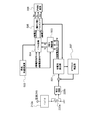
- FIG. 1 is a circuit diagram illustrating an example of a three-phase brushless motor 1 and a motor driving device 2.
- the three-phase brushless motor 1 in FIG. 1 is used, for example, as an electric actuator that generates steering assist torque in an electric power steering device of a vehicle, or as an electric actuator that drives various pumps of the vehicle.
- the motor drive device 2 that drives the three-phase brushless motor 1 includes a drive circuit 212 and a control unit 213.
- the control unit 213 includes an A / D converter 213a and a microcomputer 213b, and the microcomputer 213b includes a microprocessor such as a CPU and MPU, and a memory device such as a ROM and RAM.
- the three-phase brushless motor 1 includes a U-phase, V-phase, and W-phase three-phase windings 215u, 215v, and 215w that are star-connected to a cylindrical stator (not shown), and is formed at the center of the stator. This is a three-phase DC brushless motor that includes a permanent magnet rotor (rotor) 216 that can rotate in space.
- the three-phase brushless motor 1 does not include a sensor that detects rotor position information, and the control unit 213 performs drive control of the three-phase brushless motor 1 by a sensorless driving method that does not use a sensor that detects rotor position information.
- the three-phase brushless motor 1 is provided with a magnetic pole position sensor, and the control unit 213 can control the drive of the three-phase brushless motor 1 by detecting the rotor angle (magnetic pole position) based on the output of the magnetic pole position sensor. .
- the drive circuit 212 includes an inverter 212a in which switching elements 217a to 217f including antiparallel diodes 218a to 218f are connected in a three-phase bridge, and a DC power supply circuit 219.
- the inverter 212a is connected to the three-phase brushless motor 1. Supply AC power.
- the switching elements 217a to 217f of the inverter 212a are composed of, for example, FETs, and the control terminals (gate terminals) of the switching elements 217a to 217f are connected to the output port of the control unit 213. Then, on / off of the switching elements 217a to 217f is controlled by the control unit 213.
- the control unit 213 controls the voltage applied to the three-phase brushless motor 1 by controlling on / off of the switching elements 217a to 217f of the inverter 212a by a triangular wave comparison type PWM (Pulse Width Modulation).
- PWM Pulse Width Modulation
- the triangular wave comparison type PWM control the timing at which each switching element 217a to 217f is turned on / off by comparing the triangular wave (carrier) and the PWM timer set according to the command duty ratio (command voltage), In other words, the rising and falling timings of the PWM pulses, which are control signals for the switching elements of each phase, are detected.
- the control unit 213 is a complementary method in which the PWM pulse for controlling the on / off of the lower arm of each phase is opposite to the PWM pulse for controlling the on / off of the upper arm of each phase.
- the switching elements 217a to 217f are PWM controlled.
- a current detector 220 for detecting the DC bus current of the inverter 212a is provided between the lower arm (switching elements 217b, 217d, 217f) of each phase and the ground side of the power supply circuit 219.
- the current detector 220 includes a shunt resistor 220a connected in series between the lower arm of each phase and the ground side of the power supply circuit 219, and a detection circuit 220b including an operational amplifier.
- the detection circuit 220b detects a voltage proportional to the current generated by the resistance of the shunt resistor 220a, and outputs an analog signal of the voltage.
- the voltage analog signal (DC bus current detection signal) of the detection circuit 220b is A / D converted by the A / D converter 213a and read into the microcomputer 213b.
- the control unit 213 determines the three-phase command voltages Vu, Vv, and Vw by a vector control method based on the rotor position and the command torque, and performs PWM control of the inverter 212a based on the command voltage.
- the controller 213 receives the output of the current detector 220, detects the phase current of each phase, and performs vector control using the detected phase current.
- the current detector 220 detects the DC bus current of the inverter 212a, but the output of the current detector 220 detects that the phase current of one phase is detected by the combination of on / off of the PWM pulse of each phase. Utilizing this, the control unit 213 detects the phase current of each phase from the output of the current detector 220.
- the current detector 220 detects the W-phase current Iw.
- the control unit 213 detects the current of each phase from the output of the current detector 220 using such characteristics, and uses the detected phase current value for PWM control.
- FIG. 2 is a functional block diagram of the control unit 213 and shows a setting process of the three-phase command voltages Vu, Vv, and Vw by the vector control method.
- the phase current detection unit 501 (phase current detection means) is based on the A / D conversion value of the output of the detection circuit 220b, in other words, the phase current Iu, Iv, Iw is detected. That is, the phase current detection unit 501 sets a PWM pulse interval in which one or two of the upper arms of each phase are ON as a phase current detection interval, and based on which phase of the upper arm is ON. One phase in which the phase current is detected in the phase current detection section is specified.
- the phase current detection unit 501 sets the phase current detection timing (sampling timing of the A / D conversion value of the output of the detection circuit 220b) within the phase current detection section, and the current detector 220 at this phase current detection timing.
- the current value obtained from the sampling value is used as the phase current detection value of the phase specified as the detection target at that time.
- the angle / angular velocity calculator 502 estimates the motor angle (magnetic pole position) and angular velocity (motor rotation speed).
- the angle / angular velocity calculation unit 502 estimates the rotor position based on the counter electromotive force of the motor, and sets the estimated rotor position to the estimated rotor position. Based on this, the angular velocity is calculated.
- the angle / angular velocity calculator 502 detects the rotor position from the output of the magnetic pole position sensor, and calculates the angular velocity based on the detected rotor position.
- the three-phase / two-axis converter 503 converts the phase current detection values Iu, Iv, and Iw from the phase current detection unit 501 into a two-axis rotational coordinate system (d) based on the motor angle (magnetic pole position) ⁇ at that time.
- the vector control unit 504 includes a d-q coordinate system obtained by the d-axis command current and the q-axis command current corresponding to the command torque, the angular velocity calculated by the angle / angular velocity calculation unit 502, and the three-phase / two-axis converter 503. Real currents Id and Iq are input.
- the vector control unit 504 determines the command voltages Vq and Vd of the dq coordinate system based on the d-axis and q-axis command currents, the angular velocity, and the actual currents Id and Iq, and sets the determined command voltages Vq and Vd to 2 Output to the axis-3 phase converter 505.
- the two-axis / three-phase converter 505 converts the command voltages Vq and Vd output from the vector control unit 504 into three-phase command voltages Vu, Vv, and Vw and outputs them to the PWM modulation unit 506.
- the 2-axis to 3-phase converter 505 has a pulse shift processing function for shifting the PWM pulse generated around the valley of the triangular wave carrier back and forth by correcting the command voltages Vu, Vv, and Vw.
- the above-described pulse shift process is a process performed to secure a phase current detection interval, and will be described in detail later.
- the PWM modulation unit 506 the rising and falling timings of the switching gate waveform (PWM pulse) for driving the switching elements (upper arm and lower arm) of each phase are determined based on the three-phase command voltage Vu as a modulation wave. , Vv, Vw and the triangular wave carrier, and outputs to the control terminals (gate terminals) of the switching elements 217a to 217f of the inverter 212a.
- the PWM modulation unit 506 compares the U-phase command voltage Vu with the triangular wave carrier, and when the U-phase command voltage Vu is larger than the triangular wave carrier, the switching gate for driving the U-phase upper arm (switching element 217a).
- the waveform (PWM pulse) is set to the high level
- the switching gate waveform (PWM pulse) for driving the upper arm (switching element 217a) of the U phase when the U-phase command voltage Vu is smaller than the triangular wave carrier is set to the low level.
- the PWM modulation unit 506 drives the inverted signal of the switching gate waveform (PWM pulse) for driving the U-phase upper arm (switching element 217a) and the U-phase lower arm (switching element 217b). Generated as a switching gate waveform (PWM pulse). Similarly, the PWM modulation unit 506 generates a switching gate waveform (PWM pulse) for driving the V-phase upper and lower arms and a switching gate waveform (PWM pulse) for driving the W-phase upper and lower arms. .
- the control unit 213 includes an offset correction unit (offset correction unit) 507 that corrects an offset error of the current detector 220.
- the offset correction unit 507 obtains an offset error of the current detector 220 based on the three-phase phase currents Iu, Iv, and Iw detected by the phase current detection unit 501 based on the output of the current detector 220, and performs an offset based on the offset error.
- a correction amount is determined, and the current value detected by the current detector 220 is corrected based on the offset correction amount.
- phase current detection process in the phase current detection unit 501 will be described in detail.
- the vector control unit 504 performs calculation processing of the command voltages Vq and Vd by detecting the two-phase phase current detection values detected from the output of the current detector 220 and the remaining one-phase phase current value calculated based on these values. Can be used.
- the phase current detector 501 detects all three phase currents from the output of the current detector 220. That is, when the offset voltage of the operational amplifier constituting the current detector 220 fluctuates due to a change in ambient temperature or the like and an offset error occurs in the current detection value, the offset error is added to the phase current detection value of each phase, As a result, the sum of the three-phase phase current detection values deviates from zero.
- the amount of deviation from zero of the sum of the phase current detection values is the sum of offset errors added to the phase current detection values of each phase, and the offset error added to the individual current detection values from the amount of deviation. Therefore, when the offset error is obtained, the phase current detection unit 501 detects the three-phase phase currents from the output of the current detector 220, and the detected three-phase phase currents are offset correction units. Output to 507. Then, the offset correction unit 507 calculates an offset error based on the sum of the phase current detection values of the three phases, determines an offset correction amount based on the calculated offset error, stores the offset correction amount, and stores the offset stored in the memory. Based on the correction amount, the current detection value by the current detector 220 is offset-corrected.
- phase current detection part 501 phase current detection part 501
- the routine shown in the flowchart of FIG. 3 is interrupted by the control unit 213 every predetermined time.
- step S101 the control unit 213 determines whether or not an execution condition for the offset correction amount update processing is satisfied. For example, the control unit 213 determines that the elapsed time from the previous update process exceeds a predetermined time or that there is no failure in the current detector 220, the inverter 212a, or the like as an execution condition.
- the control unit 213 proceeds to step S102, and the phase of the PWM pulse for detecting the phase current of two to one phase in the first PWM cycle in the PWM control. Is shifted to the front and back, and a phase current detection section for detecting a phase current of two to one phase from the output of the current detector 220 is generated in the first PWM period.
- the phase current detection in the routine shown in the flowchart of FIG. 3 is configured to detect a three-phase phase current in two PWM control cycles, as will be described later.
- the first cycle is the first PWM cycle
- the immediately following cycle is the second PWM cycle.
- step S103 sets the phase current detection timing within the phase current detection section generated by the pulse shift of step S102, and samples the output of the current detector 220 at this phase current detection timing. Two-phase to one-phase phase current is detected.
- step S104 the control unit 213 proceeds to step S104, and performs a pulse shift process of the PWM pulse in a pattern different from the first PWM cycle in the second PWM cycle immediately after the first PWM cycle, A phase current detection period in which the remaining phase currents of one or two phases that are not detected in the first PWM period are detected from the output of the current detector 220 is generated in the second PWM period.
- control unit 213 changes the phase relationship between the PWM pulses of the respective phases in the first PWM cycle and the second PWM cycle, and detects the phase current in the first PWM cycle and the phase in which the phase current is detected in the second PWM cycle. And sort.
- control unit 213 proceeds to step S105, sets the phase current detection timing within the phase current detection section generated by the pulse shift of step S104, and samples the output of the current detector 220 at this phase current detection timing. A phase current of one to two phases is detected.
- the control unit 213 detects the three-phase phase currents Iu, Iv, and Iw from the output of the current detector 220 in two PWM periods. As described above, if the configuration is such that the three-phase phase current is detected in two cycles of the first PWM cycle and the second PWM cycle by the pulse shift in the first PWM cycle and the pulse shift in the second PWM cycle, the PWM pulse Thus, the three-phase phase current can be detected in the various patterns, and the detection frequency of the offset error can be improved.
- An offset error amount ⁇ I of the current detector 220 due to a temperature change or the like is added to each phase current detection value Iu, Iv, Iw, and if the true phase current values are Iuo, Ivo, Iwo, detection including an offset error
- step S107 the control unit 213 proceeds to step S107, and updates the offset correction amount for correcting the detected current value of the current detector 220 based on the offset error amount ⁇ I.
- the offset error amount ⁇ I calculated in S107 this time is a fluctuation amount of the offset error amount ⁇ I, and the control unit 213 determines in step S107. Then, the offset correction amount is changed by the variation of the offset error amount ⁇ I.
- the control unit 213 obtains the offset error amount ⁇ I a plurality of times, obtains the average value thereof, can change the offset correction amount based on the average value, and obtains the offset correction amount up to the previous time and this time. An average value of the offset correction amount based on the offset error amount ⁇ I can be used as the updated offset correction amount.
- the control unit 213 determines that the current detection accuracy by the current detector 220 is deteriorated even if the offset correction is performed, and detects the phase current detection value. The motor control based on can be stopped.
- the control unit 213 (offset correction means) performs offset correction on the detected current value by the current detector 220 using the offset correction amount updated in step S107, and performs vector control and magnetic pole position using the detected current value after offset correction. And so on.
- the processing (first detection means) in steps S102 to S105 will be described in detail based on a specific example.
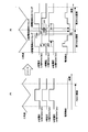
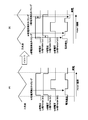
- FIG. 4 illustrates the pulse shift processing and the phase current detection timing when the widths of the three-phase PWM pulses (the three-phase command voltage) are the same.
- the width of the three-phase PWM pulse is the same, so the on-period of the PWM pulse is all three phases. There is no period in which only one-phase or two-phase PWM pulses are on, and the current flowing through one phase cannot be detected by the current detector 220.
- the phase of the V-phase PWM pulse is delayed by the time ⁇ t1 in the first PWM cycle, and the phase of the W-phase PWM pulse is further changed to the time ⁇ t2 ( ⁇ t2> ⁇ t1).
- a pulse shift process that delays only by this is performed.
- the control unit 213 corrects the command voltage using the triangular wave carrier as a reference for correction timing, thereby controlling the rising and falling timings of the PWM pulse and shifting the phase of the PWM pulse.
- Period P1 (period of time ⁇ t1) is a period in which the U-phase PWM pulse is off and the V-phase and W-phase PWM pulses are on. In this period P1, the currents flowing in the V-phase and W-phase are merged. And flows into the U phase. Therefore, the control unit 213 sets the U-phase current detection timing within the period P1, samples the output of the current detector 220 at the U-phase current detection timing, and obtains the U-phase phase current detection value Iu.
- the W-phase after the V-phase PWM pulse falls.
- the period P2 until the PWM pulse falls is a period in which the U-phase and V-phase PWM pulses are off and the W-phase PWM pulse is on.
- the control unit 213 sets the W-phase current detection timing in the period P2, samples the output of the current detector 220 at the W-phase current detection timing, and obtains the W-phase phase current detection value Iw.
- the control unit 213 delays the V-phase PWM pulse by ⁇ t1 in the first PWM cycle, and further delays the W-phase PWM pulse by ⁇ t2 ( ⁇ t2> ⁇ t1).
- the two-phase phase currents Iu and Iw of the U phase and the W phase are detected in the latter half of the first PWM cycle.
- the control unit 213 detects a section in which the V-phase current Iv can be detected in the second PWM cycle immediately after the first PWM cycle. A pulse shift process for generation is performed.
- the control unit 213 performs a process of advancing the phase of the V-phase PWM pulse by time ⁇ t3. If the control unit 213 advances only the V-phase PWM pulse by the time ⁇ t3 in the second PWM cycle, the period P3 in which the U-phase and W-phase PWM pulses are off and the V-phase PWM pulse is on (period of time ⁇ t3) ) Is generated in the first half of the second PWM cycle, and during this period P3, the current flowing in the V phase flows separately into the U phase and the W phase. Accordingly, the control unit 213 sets the V-phase current detection timing in the period P3, samples the output of the current detector 220 at this V-phase current detection timing, and obtains the V-phase phase current detection value Iv.
- the control unit 213 detects the V-phase current Iv in the first half of the second PWM cycle by performing a pulse shift process that advances the V-phase PWM pulse by the time ⁇ t3 in the second PWM cycle.
- the current detector 220 detects the phase currents of all three phases in two cycles of the first PWM cycle and the second PWM cycle.
- the delay times ⁇ t1, ⁇ t2, and ⁇ t3 are set such that the lengths of the periods P1, P2, and P3 are longer than the minimum time required for current detection, and each phase current detection timing is set to the first PWM cycle.
- the second PWM cycle are set close to each other, and the time from when the U-phase current Iu is first detected until the V-phase current Iv is finally detected is set to be as short as possible.
- the phase currents of the three phases are detected in the two periods of the first PWM period and the second PWM period, if the time from the first phase current detection timing to the last phase current detection timing becomes longer, the phase current The detection accuracy of the offset error is affected by the time change of the. Therefore, by detecting the two-phase phase current in the second half of the first PWM cycle and detecting the remaining one-phase phase current in the first half of the second PWM cycle, the section in which the three-phase phase current is detected is shortened. Furthermore, the two-phase phase current detection timing in the second half of the first PWM cycle is delayed as much as possible, and the one-phase phase current detection timing in the first half of the second PWM cycle is advanced as much as possible to shorten the three-phase phase current. To be detected.
- the control unit 213 performs a pulse shift that delays the phase of the V-phase PWM pulse in the second PWM cycle, so that the V-phase PWM pulse is off and the other phase A period in which the PWM pulse is on can be generated, and the V-phase current Iv can be detected in the first half of the second PWM cycle.
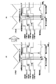
- the phase of the V-phase PWM pulse is delayed in the second PWM cycle as shown in FIG. 5A, compared with the case where the phase of the V-phase PWM pulse is advanced as shown in FIG.
- the detection timing of the phase current Iv of the V phase is delayed, and as a result, the length of the section in which the phase currents of all three phases are detected becomes longer, and the detection accuracy of the offset error decreases.
- control unit 213 performs a process of delaying the phase of the PWM pulse so that the current detection interval is set as late as possible in the first PWM cycle, and the PWM pulse so that the current detection interval is set as early as possible in the second PWM cycle.
- a process of advancing the phase of the three phases is performed so that the phase currents of the three phases can be detected in a short time.
- the control unit 213 differs from the pattern of FIG. 4 in two phases that delay the phase of the PWM pulse in the first PWM cycle and one phase that advances the phase of the PWM pulse in the second PWM cycle, for example, the first PWM cycle.
- the pulse shift process for delaying the phase of the U-phase PWM pulse is performed, and further, the pulse shift process for delaying the phase of the V-phase PWM by a larger amount than the U phase is performed in the first PWM period, and the U-phase PWM pulse is delayed in the second PWM period. If a pulse shift process for advancing the phase of the PWM pulse is performed, the phase currents Iv and Iw of the V phase and the W phase are detected in the second half of the first PWM cycle, and the phase current Iu of the U phase is detected in the first half of the second PWM cycle. can do.
- control unit 213 sets the phase that delays the phase of the PWM pulse in the first PWM cycle to only one phase, sets the phase that advances the phase of the PWM pulse in the second PWM cycle to two phases, and phase current of one phase in the first PWM cycle And the two-phase phase current remaining in the second PWM cycle can be detected. For example, a pulse shift process for delaying the phase of the V-phase PWM pulse in the first PWM period is performed, a pulse shift process for advancing the phase of the V-phase PWM pulse in the second PWM period, and a W shift in the second PWM period.
- the V phase current Iv is detected in the first PWM cycle, and the U phase and W phase current Iu in the second PWM cycle. , Iw can be detected.
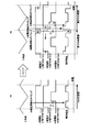
- FIG. 6 exemplifies pulse shift processing and phase current detection timing when two phases are the same and three phases are different among the widths of three-phase PWM pulses.
- the example shown in FIG. 6 is the case where the U-phase and V-phase PWM pulse widths are the same, and the W-phase PWM pulse width is shorter than the U-phase and V-phase PWM pulse widths.
- FIG. 6A shows the phase state of the PWM pulse of each phase before the pulse shift process.
- the pulse shift is not performed, during the period P4 in which the U-phase and V-phase PWM pulses are on and the W-phase PWM pulse width is off, the currents that flow into the U-phase and V-phase are merged and the W-phase Therefore, a period in which the W-phase current Iw can be detected from the output of the current detector 220 is not generated, but no section in which the U-phase and V-phase currents Iu and Iv can be detected is generated.
- the control unit 213 advances the phase of the U-phase PWM pulse in the first PWM period, and further delays the phase of the V-phase PWM pulse in the first PWM period.
- a period P5 in which the V-phase PWM pulse is on and the U-phase and W-phase PWM pulses are off is generated, and the V-phase current Iv is obtained from the output of the current detector 220 in the period P5. To detect.
- control unit 213 advances the phase of the U-phase PWM pulse in the second PWM cycle immediately after the first PWM cycle, and further delays the phase of the V-phase PWM pulse so that only the U-phase PWM pulse is turned on.
- the U-phase phase current Iu and the W-phase phase current Iw are detected in the first half of the second PWM period.
- the control unit 213 performs both the process of advancing the phase of the U-phase PWM pulse and the process of delaying the phase of the V-phase PWM pulse.
- the U-phase and V-phase PWM pulse widths are close to one cycle of PWM control, and a sufficiently long current detection interval can be obtained even if only one of the U-phase and V-phase pulse shift processing is performed. This is because it cannot be generated.
- the control unit 213 performs only the process of delaying the phase of the V-phase PWM pulse in the first PWM cycle. In some cases, the phase current Iv of the phase can be detected. Similarly, the process of advancing the phase of the U-phase PWM pulse and the process of delaying the phase of the V-phase PWM pulse in the second PWM cycle are processes for ensuring the length of the U-phase phase current detection interval.
- the control unit 213 detects the W-phase current Iw in a period P8 in which only the W-phase PWM pulse in the latter half of the first PWM period is off, and the V-phase phase is detected in the first PWM period.
- the current Iv and the W-phase current Iw can be detected, and the U-phase current Iu can be detected in the second PWM cycle.
- the control unit 213 delays the phase by the pulse shift process by performing the pulse shift process of the U-phase and V-phase PWM pulses that are longer than the W-phase PWM pulse.
- the three-phase phase current is detected in a short interval from the second half of the first PWM cycle to the first half of the second PWM cycle while suppressing the time for the advancement or advancement.
- FIG. 7 shows an example of the pulse shift process when the U-phase and V-phase PWM pulses are the same among the three-phase PWM pulses and the W-phase PWM pulse is shorter than the others.
- the control unit 213 delays the phases of the V-phase and W-phase PWM pulses in the first PWM cycle, and generates the U-phase phase current Iu detection period P9 and the W-phase phase current Iw detection period P10.
- a process for advancing the phase is performed so that the V-phase PWM pulse first rises in the second PWM cycle, and the V-phase current Iv detection period P11 is generated.
- the control unit 213 sets the offset correction amount. The update process can be canceled.
- FIG. 8 exemplifies setting of pulse shift processing and current detection timing when the PWM pulse widths are all different in three phases.
- the PWM pulse width of each phase has a relationship of U-phase PWM pulse width> W-phase PWM pulse width> V-phase PWM pulse width, and the W-phase PWM pulse width and the V-phase PWM pulse The width is approximate.
- the control unit 213 delays the phase of the V-phase PWM pulse in the first PWM cycle so that it is turned on after the time when the U-phase PWM pulse falls.
- the U-phase and V-phase phase currents Iu and Iv are detected in one PWM cycle, and in the second PWM cycle, a process for advancing the phase of the W-phase PWM pulse is performed together with a pulse shift process for delaying the phase of the U-phase PWM pulse.
- the W-phase PWM pulse is turned on before the rise time of the U-phase PWM pulse, and the W-phase current Iw is detected in the period P12 in which only the W-phase PWM pulse is on.
- the control unit 213 can be configured as shown in FIG. By performing the pulse shift process as shown, it is possible to detect a three-phase phase current in a shorter time.
- the above-exemplified pulse shift processing for detecting the three-phase phase current in the PWM2 cycle from the output of the current detector 220 is an example, and it is obvious that it can be set as appropriate according to the PWM pulse width of each phase.
- control unit 213 detects the phase current of one to two phases in the first PWM cycle and sets the PWM pulse width of each phase so as to detect the two to one phase current remaining in the first half of the second PWM cycle. Accordingly, the pulse shift processing pattern can be appropriately selected.
- the control unit 213 detects the three-phase phase current in the PWM2 cycle when performing the offset correction amount update process, but the control unit 213 detects the three-phase in the PWM2 cycle.
- the processing for detecting the phase current of the current and the processing for detecting the phase current of the three phases in the PWM1 cycle can be used properly.
- the flowchart of FIG. 9 is a control for selectively using a process for detecting a three-phase phase current in the PWM2 period (first detection means) and a process for detecting all the three-phase phase currents in the PWM1 period (second detection means). An example is shown.
- step S201 the control unit 213 determines whether or not an execution condition for the offset correction amount update processing is satisfied. If the execution condition is satisfied, the control unit 213 proceeds to step S202 (selection operation means) to detect the three-phase phase current in the PWM1 cycle and the three-phase phase current in the PWM2 cycle. Which of the detection conditions is satisfied is determined from the state of the PWM pulse width of each phase at that time.
- the control unit 213 performs 3 in the PWM2 cycle. It is determined that the first condition for detecting the phase current of the phase is satisfied, and the PWM pulse width state of each phase can detect the three-phase phase current in one PWM cycle by performing the pulse shift process.
- the second state it can be determined that the second condition for detecting the three-phase phase current in the PWM1 cycle is satisfied.
- control unit 213 determines that the second condition for detecting the three-phase phase current in the PWM1 period is satisfied when the torque command value is constant and the phase current of each phase is stable, When the torque command value varies, it can be determined that the first condition for detecting the three-phase phase current in the PWM2 period is satisfied.
- the reason for this selection condition is that when three-phase phase current is detected in one PWM cycle, the period during which all three phase currents are detected becomes longer and the detection accuracy of the offset error decreases due to fluctuations in the phase current. This is because, when the phase current is stable, a decrease in offset error detection accuracy can be suppressed even if the period during which all three phase currents are detected becomes long.
- the calculation load of the process of detecting the three-phase phase current in the PWM1 period is small, so the process of detecting the three-phase phase current in the PWM2 period as described above If the process for detecting all the three-phase phase currents in one PWM cycle is properly used, the calculation load in the control unit 213 can be suppressed.
- the control unit 213 has a constant torque command value, the phase current of each phase is stable, and can detect a three-phase phase current in the PWM1 cycle. It is determined that the second condition for detecting the phase current is satisfied, and if the second condition is not satisfied, it is determined that the first condition for detecting the three-phase phase current in the PWM2 period is satisfied. Can do.
- step S202 determines in step S202 that the first condition for detecting the three-phase phase current in the PWM2 cycle is satisfied and the second condition for detecting the three-phase phase current in the PWM1 cycle is not satisfied.
- step S203 the processing from step S203 to step S206, the three-phase phase current is detected in the PWM2 cycle. Note that the processing from step S203 to step S206 is the same as step S102 to step S105 in the flowchart of FIG. 3, and detailed description thereof will be omitted.
- step S202 the control unit 213 does not satisfy the first condition for detecting the three-phase phase current in the PWM2 cycle, and satisfies the second condition for detecting the three-phase phase current in the PWM1 cycle. If it judges, it will progress to step S207 and will carry out the pulse shift process for detecting the phase current of three phases in PWM1 period, and in the next step S208, the current will be within the current detection period of each of the three phases generated by the pulse shift process. A detection timing is set, and a three-phase phase current is detected in one PWM cycle.
- FIG. 10 exemplifies a pulse shift process for detecting a three-phase phase current in one PWM cycle and a current detection timing in the PWM pulse after the pulse shift process.
- FIG. 10A shows the PWM pulse of each phase before the pulse shift processing, the U-phase and V-phase PWM pulse widths are the same, and the W-phase PWM pulse width is greater than the U-phase and V-phase PWM pulse widths. The case where is also short is illustrated.
- the current detection period is limited to a period in which the U-phase and V-phase PWM pulses are on and the W-phase PWM pulse is off and the W-phase current Iw can be detected. An interval in which the phase current of the V phase can be detected is not generated. Therefore, the control unit 213 performs a pulse shift process as illustrated in FIG. 10B, and generates a phase current detection period for each of the three phases within the PWM1 period.
- control unit 213 performs a pulse shift process of advancing the phase of the U-phase PWM pulse while delaying the phase of the V-phase PWM pulse, so that only the U-phase PWM pulse is early in the PWM1 period. Is generated when the U phase is on and the phase current Iu of the U phase can be detected, and at the end of the PWM1 period, only the PWM pulse of the V phase is on and the phase current Iv of the V phase can be detected.
- the U-phase phase current Iu detection timing and the V-phase phase current Iv detection timing are set, and the phase currents Iu and Iv are detected from the output of the current detector 220.
- the pulse shift process is performed on both the U-phase PWM pulse and the V-phase PWM pulse because a sufficiently long current detection period cannot be generated when the pulse shift process is performed only on one phase. It is.
- the control unit 213 sets the W-phase phase current Iw detection timing within a period in which the U-phase and V-phase PWM pulses are on and the W-phase PWM pulse is off and the W-phase phase current Iw can be detected. Then, the phase current Iw is detected from the output of the current detector 220. It is obvious that various combinations other than those illustrated in FIG. 10 can be used for combinations of PWM pulse widths and patterns of pulse shift processing in the case of detecting a three-phase phase current in one PWM cycle.
- the control unit 213 can use the three-phase phase currents Iu, Iv, and Iw detected from the output of the current detector 220 in the PWM 2 cycle for vector control of the three-phase brushless motor 1.
- the control unit 213 when detecting the three-phase phase current from the output of the current detector 220, the control unit 213 performs a process of suppressing the fluctuation of the torque command value (command voltage of each phase), and the torque command value (each It is possible to detect a three-phase phase current in a stable state of the phase command voltage.
- SYMBOLS 1 Three-phase brushless motor, 2 ... Motor drive device, 212 ... Drive circuit, 212a ... Inverter, 213 ... Control part, 213a ... A / D converter, 213b ... Microcomputer, 220 ... Current detector, 220a ... Shunt resistance , 220b ... detection circuit
Landscapes
- Engineering & Computer Science (AREA)
- Power Engineering (AREA)
- Control Of Motors That Do Not Use Commutators (AREA)
- Control Of Ac Motors In General (AREA)
- Inverter Devices (AREA)
Abstract
Description
係る温度変化などによる電流検出値のオフセット誤差は3相それぞれの相電流検出値に付加されることになる一方、3相の相電流の総和は零になるから、3相それぞれの相電流を電流検出器で検出することでオフセット誤差を求めることができる。
そして、オフセット誤差に応じて電流検出値を補正するオフセット補正を行うことで、温度変化があっても相電流の検出精度が維持され、引いては、モータトルクの制御精度が維持される。
このため、各相のデューティ指令値をキャリア周期の所定位置に固定する方式での相電流検出処理では、オフセット誤差の検出頻度(オフセット補正量の更新頻度)が低くなり、温度環境の変化に対してオフセット補正量を応答よく追従させることができずに相電流の検出精度が低下してしまう可能性があった。
したがって、電流検出のオフセット誤差を全相の相電流検出値に基づき求めて電流検出値をオフセット補正する場合は、オフセット補正値の更新頻度が高まると共に高い精度でオフセット補正値を求めることができる。
図1は、3相ブラシレスモータ1及びモータ駆動装置2の一例を示す回路図である。
図1の3相ブラシレスモータ1は、例えば、車両の電動パワーステアリング装置において操舵のアシストトルクを発生する電動アクチュエータとして用いられたり、車両の各種ポンプを駆動する電動アクチュエータとして用いられる。
制御部213は、A/D変換器213aとマイクロコンピュータ213bとを備え、マイクロコンピュータ213bは、CPU,MPUなどのマイクロプロセッサやROM、RAMなどのメモリデバイスを含んで構成される。
3相ブラシレスモータ1は、スター結線されるU相、V相及びW相の3相巻線215u、215v、215wを図示省略した円筒状の固定子に備え、該固定子の中央部に形成した空間に永久磁石回転子(ロータ)216を回転可能に備える、3相DCブラシレスモータである。
但し、3相ブラシレスモータ1に磁極位置センサを備え、制御部213は、係る磁極位置センサの出力に基づきロータの角度(磁極位置)を検出して3相ブラシレスモータ1を駆動制御することができる。
インバータ212aのスイッチング素子217a~217fは例えばFETで構成され、スイッチング素子217a~217fの各制御端子(ゲート端子)は制御部213の出力ポートに接続される。そして、スイッチング素子217a~217fのオン/オフは制御部213によって制御される。
三角波比較方式のPWM制御においては、三角波(キャリア)と、指令デューティ比(指令電圧)に応じて設定されるPWMタイマとを比較することで、各スイッチング素子217a~217fをオン/オフさせるタイミング、換言すれば、各相のスイッチング素子の制御信号であるPWMパルスの立ち上げ及び立ち下げのタイミングを検出する。
なお、制御部213は、各相の上アームのオン/オフを制御するPWMパルスに対し、各相の下アームのオン/オフを制御するPWMパルスを逆相とする相補方式で、インバータ212aのスイッチング素子217a~217fをPWM制御する。
電流検出器220は、各相の下アームと電源回路219の接地側との間に直列に接続したシャント抵抗220aと、オペアンプなどを含む検出回路220bとから構成される。検出回路220bは、シャント抵抗220aの抵抗分で発生する電流に比例した電圧を検出し、係る電圧のアナログ信号を出力する。
制御部213は、例えば、回転子位置と指令トルクとに基づくベクトル制御方式によって3相指令電圧Vu、Vv、Vwを決定し、この指令電圧に基づきインバータ212aをPWM制御する。
電流検出器220は、インバータ212aの直流母線電流を検出するが、各相のPWMパルスのオン/オフの組み合わせによって電流検出器220の出力が1つの相の相電流を検出する状態となることを利用して、制御部213は、各相の相電流を電流検出器220の出力から検出する。
このように、各相の上アームのうちの1つ又は2つがオンであるPWMパルスの状態において、電流検出器220の出力は、パルス状態で決まる1つの相の相電流を表すことになる。そこで、制御部213は、係る特性を利用して電流検出器220の出力から各相の電流を検出し、検出した相電流値をPWM制御に用いる。
図2において、相電流検出部501(相電流検出手段)は、検出回路220bの出力のA/D変換値、換言すればインバータ212aの直流母線電流に基づき、各相の相電流Iu、Iv、Iwを検出する。
つまり、相電流検出部501は、各相の上アームのうちの1つ又は2つがオンであるPWMパルス区間を相電流検出区間とし、また、いずれの相の上アームがオンであるかに基づき前記相電流検出区間で相電流が検出される1つの相を特定する。
角度・角速度演算部502は、モータ角度(磁極位置)及び角速度(モータ回転数)を推定する。
ベクトル制御部504には、指令トルクに応じたd軸指令電流及びq軸指令電流、角度・角速度演算部502で算出された角速度、3相-2軸変換器503で求めたd-q座標系の実電流Id,Iqが入力される。
2軸-3相変換器505は、ベクトル制御部504が出力する指令電圧Vq,Vdを3相指令電圧Vu、Vv、Vwに変換してPWM変調部506に出力する。
そして、PWM変調部506では、各相のスイッチング素子(上アーム及び下アーム)を駆動するためのスイッチングゲート波形(PWMパルス)の立ち上げ、立ち下げタイミングを、変調波としての3相指令電圧Vu、Vv、Vwと三角波キャリアとの比較によって決定し、インバータ212aの各スイッチング素子217a~217fの各制御端子(ゲート端子)に出力する。
同様にして、PWM変調部506は、V相の上下アームを駆動するためのスイッチングゲート波形(PWMパルス)、及び、W相の上下アームを駆動するためのスイッチングゲート波形(PWMパルス)を生成する。
オフセット補正部507は、相電流検出部501が電流検出器220の出力に基づき検出した3相の相電流Iu、Iv、Iwに基づき電流検出器220のオフセット誤差を求め、当該オフセット誤差に基づきオフセット補正量を定め、係るオフセット補正量に基づき電流検出器220で検出される電流値を補正する。
インバータ212aの直流母線電流に基づき各相の相電流を検出する場合、2相の相電流を電流検出器220の出力から検出できれば、残りの1相の電流は相電流の総和が零になることを用いて演算により求めることができる。
そして、ベクトル制御部504は、指令電圧Vq,Vdの演算処理を、電流検出器220の出力から検出した2相の相電流検出値と、これらに基づき演算した残る1相の相電流値とを用いて行える。
つまり、電流検出器220を構成するオペアンプのオフセット電圧が周囲温度の変化などにより変動して電流検出値にオフセット誤差が生じた場合、係るオフセット誤差は各相の相電流検出値にそれぞれ付加され、これにより3相の相電流検出値の総和が零からずれることになる。
そして、オフセット補正部507は、3相それぞれの相電流検出値の総和に基づきオフセット誤差を算出し、算出したオフセット誤差に基づきオフセット補正量を決定してメモリに格納し、メモリに格納されたオフセット補正量に基づき電流検出器220による電流検出値をオフセット補正する。
図3のフローチャートに示すルーチンは、制御部213によって所定時間毎に割り込み実行される。
制御部213は、例えば、前回の更新処理からの経過時間が所定時間を超えていることや、電流検出器220やインバータ212aなどに故障がないことなどを実行条件として判別する。
なお、図3のフローチャートに示すルーチンにおける相電流の検出は、後述するようにPWM制御の2周期で3相の相電流を検出するよう構成され、このPWM制御の2周期を1単位とするときの始めの1周期を第1PWM周期とし、直後の1周期を第2PWM周期とする。
第1PWM周期で相電流の検出を行うと、制御部213は、ステップS104へ進み、第1PWM周期直後の第2PWM周期においてPWMパルスのパルスシフト処理を第1PWM周期とは異なるパターンで実施して、第1PWM周期で相電流を検出していない残る1相乃至2相の相電流を電流検出器220の出力から検出する相電流検出区間を第2PWM周期に生成する。
次いで、制御部213は、ステップS105に進み、ステップS104のパルスシフトで生成した相電流検出区間内に相電流検出タイミングを設定し、この相電流検出タイミングで電流検出器220の出力をサンプリングして、1相乃至2相の相電流を検出する。
そして、制御部213は、ステップS106に進み、相電流検出値Iu、Iv、Iwの総和を3で割った値を、オフセット誤差量ΔIとして算出する(ΔI=(Iu+Iv+Iw)/3)。
各相電流検出値Iu、Iv、Iwがオフセット補正後の値である場合、今回S107で演算されたオフセット誤差量ΔIは、オフセット誤差量ΔIの変動分となり、制御部213は、ステップS107にて、オフセット誤差量ΔIの変動分だけオフセット補正量を変更する。
また、オフセット誤差量ΔIが閾値を超える値である場合、制御部213は、たとえオフセット補正を行ったとしても電流検出器220による電流の検出精度が悪化するものと判断し、相電流の検出値に基づくモータ制御を停止することができる。
ここで、ステップS102-ステップS105での処理(第1検出手段)を、具体例に基づき詳細に説明する。
図4(A)のパルスシフト処理前の状態(三角波キャリアの谷をPWMパルスの中心とする標準状態)では、3相のPWMパルスの幅が同じであるためPWMパルスのオン期間が3相全てで重なっていて、1相又は2相のPWMパルスのみがオンである期間がなく、電流検出器220によって1つの相に流れる電流を検出できない。
制御部213は、三角波キャリアを補正タイミングの基準として指令電圧を補正することで、PWMパルスの立ち上がり及び立ち下がりのタイミングを制御し、PWMパルスの位相をシフトさせる。
上記の第1PWM周期におけるパルスシフト処理ではV相の相電流Ivを検出できる区間が生成されないので、制御部213は、第1PWM周期直後の第2PWM周期でV相の相電流Ivを検出できる区間を生成するためのパルスシフト処理を実施する。
第2PWM周期で制御部213がV相のPWMパルスのみを時間Δt3だけ進ませれば、U相及びW相のPWMパルスがオフでV相のPWMパルスがオンである期間P3(時間Δt3の期間)が第2PWM周期の前半に生成されることになり、この期間P3ではV相に流れた電流がU相及びW相に分かれて流れる。したがって、制御部213は、期間P3にV相電流検出タイミングを設定し、このV相電流検出タイミングで電流検出器220の出力をサンプリングして、V相の相電流検出値Ivを求める。
なお、遅延時間Δt1、Δt2、Δt3は、前記期間P1、P2、P3の長さが電流検出に必要な最小時間よりも長くなるように設定され、更に、各相電流検出タイミングが、第1PWM周期と第2PWM周期との境界近く設定され、最初にU相の相電流Iuが検出されてから最後にV相の相電流Ivが検出されるまでの時間が極力短くなるように設定される。
そこで、第1PWM周期の後半で2相の相電流を検出し第2PWM周期の前半で残りの1相の相電流を検出させることで、3相の相電流が検出される区間が短くするが、更に、第1PWM周期の後半での2相の相電流検出タイミングを極力遅らせ、また、第2PWM周期の前半での1相の相電流検出タイミングを極力早めることで、3相の相電流が短時間で検出されるようにする。
なお、制御部213は、第1PWM周期でPWMパルスの位相を遅らせる2つの相、第2PWM周期でPWMパルスの位相を進ませる1つの相を図4のパターンとは異ならせ、例えば、第1PWM周期でU相のPWMパルスの位相を遅らせるパルスシフト処理を実施し、更に、第1PWM周期でV相のPWMの位相をU相よりも大きく遅らせるパルスシフト処理を実施し、第2PWM周期でU相のPWMパルスの位相を進ませるパルスシフト処理を実施すれば、第1PWM周期の後半でV相とW相の相電流Iv、Iwを検出させ、第2PWM周期の前半でU相の相電流Iuを検出することができる。
例えば、第1PWM周期でV相のPWMパルスの位相を遅らせるパルスシフト処理を実施し、第2PWM周期でV相のPWMパルスの位相を進ませるパルスシフト処理を実施し、更に、第2PWM周期でW相のPWMパルスの位相をV相よりも大きく進ませるパルスシフト処理を実施することで、第1PWM周期でV相の相電流Ivを検出させ、第2PWM周期でU相及びW相の相電流Iu、Iwを検出することができる。
図6に示す例は、U相及びV相のPWMパルス幅が同じで、W相のPWMパルス幅がU相及びV相のPWMパルス幅よりも短い場合である。
同様に、第2PWM周期におけるU相のPWMパルスの位相を進ませる処理及びV相のPWMパルスの位相を遅らせる処理は、U相の相電流検出区間の長さを確保するための処理である。
また、制御部213は、図6に示す例において、W相のPWMパルスに比べて幅が長いU相及びV相のPWMパルスのパルスシフト処理を実施することで、パルスシフト処理で位相を遅らせたり早めたりする時間を抑制しつつ、第1PWM周期の後半から第2PWM周期の前半にかけての短い区間で3相の相電流を検出する。
図7は、3相のPWMパルスのうちのU相及びV相のPWMパルスが同じで、W相のPWMパルスが他よりも短い場合のパルスシフト処理の例を示す。
なお、PWMパルスの幅などの条件がパルスシフト処理によってPWM2周期で3相の相電流を電流検出器220の出力から検出することが困難な条件であるときは、制御部213は、オフセット補正量の更新処理をキャンセルすることができる。
図8の例では、各相のPWMパルス幅は、U相PWMパルス幅>W相PWMパルス幅>V相PWMパルス幅の関係になっていて、かつ、W相PWMパルス幅とV相PWMパルス幅とが近似している。
そこで、制御部213は、図8(B)に示すように、第1PWM周期においてV相のPWMパルスの位相をU相のPWMパルスが立ち下がる時期以降にオンになるように遅らせることで、第1PWM周期においてU相及びV相の相電流Iu、Ivを検出し、第2PWM周期において、U相のPWMパルスの位相を遅らせるパルスシフト処理とともにW相のPWMパルスの位相を進ませる処理を実施することで、W相のPWMパルスがU相のPWMパルスの立ち上がり時期以前にオンになるようにして、このW相のPWMパルスのみがオンである期間P12でW相の相電流Iwを検出する。
上記に例示した、PWM2周期で3相の相電流を電流検出器220の出力から検出するためのパルスシフト処理は一例であり、各相のPWMパルス幅に応じて適宜設定できることは明らかである。つまり、制御部213は、第1PWM周期で1相乃至2相の相電流を検出し第2PWM周期の前半で残る2相乃至1相の相電流を検出できるように、各相のPWMパルス幅に応じてパルスシフト処理のパターンを適宜選定できる。
図9のフローチャートは、PWM2周期で3相の相電流を検出する処理(第1検出手段)と、PWM1周期で3相の相電流を全て検出する処理(第2検出手段)とを使い分ける制御の一例を示す。
そして、実行条件が成立している場合、制御部213は、ステップS202(選択作動手段)へ進んで、PWM1周期で3相の相電流を検出する条件と、PWM2周期で3相の相電流を検出する条件とのいずれが成立しているかを、そのときの各相のPWMパルス幅の状態などから判断する。
なお、制御部213は、トルク指令値が一定であって各相の相電流が安定していて、かつ、PWM1周期で3相の相電流を検出することができるときに、PWM1周期で3相の相電流を検出する第2条件が成立していると判断し、係る第2条件が成立しない場合にPWM2周期で3相の相電流を検出する第1条件が成立していると判断することができる。
なお、ステップS203-ステップS206の処理は、図3のフローチャートのステップS102-ステップS105と同じであり、詳細な説明は省略する。
図10(A)は、パルスシフト処理前の各相のPWMパルスを示し、U相及びV相のPWMパルス幅が同じで、W相のPWMパルス幅がU相及びV相のPWMパルス幅よりも短い場合を例示する。
そこで、制御部213は、図10(B)に例示するようにしてパルスシフト処理を実施し、3相それぞれの相電流検出期間をPWM1周期内に生成する。
また、制御部213は、U相及びV相のPWMパルスがオンでW相のPWMパルスがオフであってW相の相電流Iwを検出できる期間内にW相の相電流Iw検出タイミングを設定して、電流検出器220の出力から相電流Iwを検出する。
なお、PWM1周期で3相の相電流を検出する場合のPWMパルス幅の組み合わせ及びパルスシフト処理のパターンは、図10に例示した以外に種々設定できることは明らかである。
制御部213は、PWM2周期で電流検出器220の出力から検出した3相の相電流Iu,Iv,Iwを3相ブラシレスモータ1のベクトル制御に用いることができる。
Claims (8)
- 3相ブラシレスモータに交流電力を供給するインバータと、前記インバータの直流母線電流を検出する電流検出器と、前記電流検出器の出力を入力し前記インバータをPWM制御する制御部と、を含むモータ駆動装置であって、
前記制御部は、各相のPWMパルスのオン/オフの組み合わせが所定の組み合わせであるときの前記電流検出器の出力から各相の相電流を検出する相電流検出手段を備え、
前記相電流検出手段は、PWMパルスの位相をシフトさせるパルスシフト処理によって前記PWM制御の第1PWM周期と第2PWM周期とで各相のPWMパルスの位相関係を異ならせ、前記第1PWM周期と前記第2PWM周期との2周期で前記電流検出器の出力から3相それぞれの相電流を検出する第1検出手段を含む、モータ駆動装置。 - 前記第1検出手段は、前記第1PWM周期の後半で1相又は2相の電流を検出し、前記第1PWM周期の直後の前記第2PWM周期の前半で残る2相又は1相の電流を検出する、請求項1記載のモータ駆動装置。
- 前記第1検出手段は、前記第1PWM周期において前記PWMパルスの位相を遅らせるパルスシフト処理を実施し、前記第2PWM周期において前記PWMパルスの位相を進ませるパルスシフト処理を実施する、請求項2記載のモータ駆動装置。
- 前記制御部は、PWMパルスの位相をシフトさせるパルスシフト処理によって前記PWM制御の1周期で前記電流検出器の出力から3相それぞれの相電流を検出する第2検出手段と、前記第1検出手段を作動させる第1条件と前記第2検出手段を作動させる第2条件とのいずれが成立しているかに応じて前記第1検出手段と前記第2検出手段とのいずれか一方を作動させる選択作動手段と、を更に含む、請求項1記載のモータ駆動装置。
- 前記制御部は、前記相電流検出手段により検出された3相それぞれの相電流に基づき前記電流検出器による電流検出値をオフセット補正するオフセット補正手段を更に含む、請求項1記載のモータ駆動装置。
- 3相ブラシレスモータに交流電力を供給するインバータと前記インバータの直流母線電流を検出する電流検出器とを含み前記インバータがPWM制御されるモータ駆動装置において相電流を検出する方法であって、
前記PWM制御の第1PWM周期においてPWMパルスの位相をシフトさせるパルスシフト処理によって1相乃至2相の相電流検出区間を生成する第1ステップと、
前記第1PWM周期に生成された相電流検出区間における前記電流検出器の出力から前記1相乃至2相の相電流を検出する第2ステップと、
前記PWM制御の第2PWM周期においてPWMパルスの位相をシフトさせるパルスシフト処理によって残りの2相乃至1相の相電流検出区間を生成する第3ステップと、
前記第2PWM周期に生成された相電流検出区間における前記電流検出器の出力から前記残りの2相乃至1相の相電流を検出する第4ステップと、
を含む、モータ駆動装置における相電流検出方法。 - 前記第1ステップは、前記第1PWM周期においてPWMパルスの位相を遅らせるパルスシフト処理を実施して前記第1PWM周期の後半に1相乃至2相の相電流検出区間を生成し、
前記第3ステップは、前記第1PWM周期の直後である前記第2PWM周期においてPWMパルスの位相を進ませるパルスシフト処理を実施して前記第2PWM周期の前半に残りの2相乃至1相の相電流検出区間を生成する、請求項6記載のモータ駆動装置における相電流検出方法。 - 3相それぞれの相電流の検出値に基づき前記電流検出器による電流検出値をオフセット補正する第5ステップを更に含む、請求項6記載のモータ駆動装置における相電流検出方法。
Priority Applications (4)
| Application Number | Priority Date | Filing Date | Title |
|---|---|---|---|
| KR1020187024462A KR101958159B1 (ko) | 2016-03-11 | 2016-08-24 | 모터 구동 장치 및 모터 구동 장치에서의 상전류 검출 방법 |
| US16/083,853 US10840842B2 (en) | 2016-03-11 | 2016-08-24 | Motor driving device and method for measuring phase current in motor driving device |
| CN201680083203.9A CN108781053B (zh) | 2016-03-11 | 2016-08-24 | 电机驱动装置及电机驱动装置中的相电流检测方法 |
| DE112016006575.2T DE112016006575B4 (de) | 2016-03-11 | 2016-08-24 | Motoransteuervorrichtung und verfahren zum messen eines phasenstroms in einer motoransteuervorrichtung |
Applications Claiming Priority (2)
| Application Number | Priority Date | Filing Date | Title |
|---|---|---|---|
| JP2016048451A JP6529452B2 (ja) | 2016-03-11 | 2016-03-11 | モータ駆動装置及びモータ駆動装置における相電流検出方法 |
| JP2016-048451 | 2016-03-11 |
Publications (1)
| Publication Number | Publication Date |
|---|---|
| WO2017154239A1 true WO2017154239A1 (ja) | 2017-09-14 |
Family
ID=59789180
Family Applications (1)
| Application Number | Title | Priority Date | Filing Date |
|---|---|---|---|
| PCT/JP2016/074599 Ceased WO2017154239A1 (ja) | 2016-03-11 | 2016-08-24 | モータ駆動装置及びモータ駆動装置における相電流検出方法 |
Country Status (6)
| Country | Link |
|---|---|
| US (1) | US10840842B2 (ja) |
| JP (1) | JP6529452B2 (ja) |
| KR (1) | KR101958159B1 (ja) |
| CN (1) | CN108781053B (ja) |
| DE (1) | DE112016006575B4 (ja) |
| WO (1) | WO2017154239A1 (ja) |
Cited By (4)
| Publication number | Priority date | Publication date | Assignee | Title |
|---|---|---|---|---|
| WO2021014948A1 (ja) * | 2019-07-22 | 2021-01-28 | ミネベアミツミ株式会社 | モータ制御装置およびモータシステム |
| US11349412B2 (en) * | 2018-12-13 | 2022-05-31 | Nabtesco Corporation | Three-phase AC control apparatus and three-phase AC control system |
| US20230026201A1 (en) * | 2020-01-14 | 2023-01-26 | Minebea Mitsumi Inc. | Motor drive control device and motor drive control method |
| JP2023044415A (ja) * | 2021-09-17 | 2023-03-30 | 株式会社日立インダストリアルプロダクツ | 電力変換装置 |
Families Citing this family (16)
| Publication number | Priority date | Publication date | Assignee | Title |
|---|---|---|---|---|
| WO2018016356A1 (ja) * | 2016-07-20 | 2018-01-25 | 日本精工株式会社 | 電動パワーステアリング装置 |
| BR112018076801B1 (pt) * | 2016-07-20 | 2023-03-21 | Nsk Ltd | Aparelho de direção de energia elétrica |
| CN111903051B (zh) * | 2018-03-28 | 2024-07-23 | 新电元工业株式会社 | 驱动装置、电动车辆以及驱动装置的控制方法 |
| CN110858757B (zh) * | 2018-08-21 | 2022-05-24 | 广东威灵汽车部件有限公司 | 一种电流控制及采样方法、装置及计算机可读存储介质 |
| CN112740532B (zh) * | 2018-09-28 | 2023-11-07 | 三菱电机株式会社 | 电力变换装置 |
| DE102018251746A1 (de) * | 2018-12-27 | 2020-07-02 | Robert Bosch Gmbh | Verfahren zum Ermitteln eines Verstärkungsfehlers einer Strommesseinrichtung |
| JP7245057B2 (ja) * | 2019-01-22 | 2023-03-23 | 日立Astemo株式会社 | モータ制御装置 |
| IT201900006238A1 (it) * | 2019-04-23 | 2020-10-23 | Piaggio & C Spa | Sistema di controllo di un veicolo a sella cavalcabile provvisto di un azionamento elettrico |
| US10784810B1 (en) * | 2019-04-29 | 2020-09-22 | Allegro Microsystems, Llc | Motor controller with accurate current measurement |
| TWI697257B (zh) * | 2019-06-28 | 2020-06-21 | 聚積科技股份有限公司 | 補償式電流校正裝置 |
| JP7501058B2 (ja) * | 2020-03-31 | 2024-06-18 | 株式会社富士通ゼネラル | モータ制御装置 |
| JP7382885B2 (ja) * | 2020-03-31 | 2023-11-17 | ミネベアミツミ株式会社 | モータ制御装置、モータシステム及びモータ制御方法 |
| KR102797455B1 (ko) * | 2020-06-12 | 2025-04-22 | 두원중공업(주) | 전동압축기 인버터의 전류 오프셋 보정 장치 및 그 방법 |
| JP2022044290A (ja) * | 2020-09-07 | 2022-03-17 | ミネベアミツミ株式会社 | モータ制御装置、モータシステム及びモータ制御方法 |
| CN113852311A (zh) * | 2021-08-18 | 2021-12-28 | 北京精密机电控制设备研究所 | 一种容错永磁同步电机相电流采样方法 |
| JP7782396B2 (ja) * | 2022-09-09 | 2025-12-09 | 株式会社デンソー | 制御装置 |
Citations (4)
| Publication number | Priority date | Publication date | Assignee | Title |
|---|---|---|---|---|
| JP2008061486A (ja) * | 2005-10-24 | 2008-03-13 | Matsushita Electric Ind Co Ltd | インバータ装置 |
| JP2009118622A (ja) * | 2007-11-06 | 2009-05-28 | Omron Corp | 多相電動機の制御装置 |
| JP2013066340A (ja) * | 2011-09-20 | 2013-04-11 | Toshiba Corp | モータ制御装置 |
| JP2015178328A (ja) * | 2014-03-19 | 2015-10-08 | 日立オートモティブシステムズステアリング株式会社 | パワーステアリング装置およびパワーステアリング装置用制御装置 |
Family Cites Families (13)
| Publication number | Priority date | Publication date | Assignee | Title |
|---|---|---|---|---|
| JPH0947063A (ja) * | 1995-07-26 | 1997-02-14 | Konica Corp | Dcモータの速度制御装置 |
| US7560897B2 (en) * | 2005-03-29 | 2009-07-14 | Kabushiki Kaisha Yaskawa Denki | Current controller and current offset correction |
| US7855527B2 (en) | 2005-10-24 | 2010-12-21 | Panasonic Corporation | Inverter device |
| JP5069882B2 (ja) * | 2006-08-30 | 2012-11-07 | 日立アプライアンス株式会社 | 三相コンバータ・インバータ装置及びモジュール |
| JP4884355B2 (ja) | 2007-11-26 | 2012-02-29 | オムロンオートモーティブエレクトロニクス株式会社 | 多相電動機の制御装置 |
| JP5136384B2 (ja) * | 2008-12-16 | 2013-02-06 | 株式会社明電舎 | 直列多重インバータの出力電流検出方法 |
| JP5929521B2 (ja) | 2012-05-31 | 2016-06-08 | 日本精工株式会社 | モータ制御装置及びそれを用いた電動パワーステアリング装置 |
| JP5973856B2 (ja) * | 2012-09-18 | 2016-08-23 | 日立オートモティブシステムズ株式会社 | 電動パワーステアリング装置および電動パワーステアリング装置の制御装置 |
| JP5968805B2 (ja) * | 2013-02-28 | 2016-08-10 | 日立オートモティブシステムズ株式会社 | モータ装置およびモータ駆動装置 |
| BR112015026318A2 (pt) * | 2013-04-17 | 2019-08-27 | Nsk Ltd | aparelho de controle motor multi-fase e aparelho elétrico de direção utilizando o mesmo |
| JP6099148B2 (ja) * | 2013-09-04 | 2017-03-22 | オムロンオートモーティブエレクトロニクス株式会社 | モータ制御装置 |
| US9774284B2 (en) * | 2015-02-19 | 2017-09-26 | Rockwell Automation Technologies, Inc. | Rotor position estimation apparatus and methods |
| US9584043B2 (en) * | 2015-02-28 | 2017-02-28 | Rockwell Automation Technologies, Inc. | Inverter phase current reconstruction apparatus and methods |
-
2016
- 2016-03-11 JP JP2016048451A patent/JP6529452B2/ja active Active
- 2016-08-24 WO PCT/JP2016/074599 patent/WO2017154239A1/ja not_active Ceased
- 2016-08-24 KR KR1020187024462A patent/KR101958159B1/ko not_active Expired - Fee Related
- 2016-08-24 DE DE112016006575.2T patent/DE112016006575B4/de active Active
- 2016-08-24 CN CN201680083203.9A patent/CN108781053B/zh active Active
- 2016-08-24 US US16/083,853 patent/US10840842B2/en active Active
Patent Citations (4)
| Publication number | Priority date | Publication date | Assignee | Title |
|---|---|---|---|---|
| JP2008061486A (ja) * | 2005-10-24 | 2008-03-13 | Matsushita Electric Ind Co Ltd | インバータ装置 |
| JP2009118622A (ja) * | 2007-11-06 | 2009-05-28 | Omron Corp | 多相電動機の制御装置 |
| JP2013066340A (ja) * | 2011-09-20 | 2013-04-11 | Toshiba Corp | モータ制御装置 |
| JP2015178328A (ja) * | 2014-03-19 | 2015-10-08 | 日立オートモティブシステムズステアリング株式会社 | パワーステアリング装置およびパワーステアリング装置用制御装置 |
Cited By (5)
| Publication number | Priority date | Publication date | Assignee | Title |
|---|---|---|---|---|
| US11349412B2 (en) * | 2018-12-13 | 2022-05-31 | Nabtesco Corporation | Three-phase AC control apparatus and three-phase AC control system |
| WO2021014948A1 (ja) * | 2019-07-22 | 2021-01-28 | ミネベアミツミ株式会社 | モータ制御装置およびモータシステム |
| US20230026201A1 (en) * | 2020-01-14 | 2023-01-26 | Minebea Mitsumi Inc. | Motor drive control device and motor drive control method |
| JP2023044415A (ja) * | 2021-09-17 | 2023-03-30 | 株式会社日立インダストリアルプロダクツ | 電力変換装置 |
| JP7734543B2 (ja) | 2021-09-17 | 2025-09-05 | 株式会社日立インダストリアルプロダクツ | 電力変換装置 |
Also Published As
| Publication number | Publication date |
|---|---|
| CN108781053B (zh) | 2019-09-13 |
| CN108781053A (zh) | 2018-11-09 |
| KR20180098692A (ko) | 2018-09-04 |
| DE112016006575B4 (de) | 2025-03-20 |
| KR101958159B1 (ko) | 2019-03-13 |
| JP6529452B2 (ja) | 2019-06-12 |
| JP2017163789A (ja) | 2017-09-14 |
| US10840842B2 (en) | 2020-11-17 |
| US20190068098A1 (en) | 2019-02-28 |
| DE112016006575T5 (de) | 2018-11-22 |
Similar Documents
| Publication | Publication Date | Title |
|---|---|---|
| JP6529452B2 (ja) | モータ駆動装置及びモータ駆動装置における相電流検出方法 | |
| CN107509393B (zh) | 电机驱动装置及3相无刷电机的相电流检测方法 | |
| JP7102407B2 (ja) | インバータ装置、及び、電動パワーステアリング装置 | |
| CN103580587B9 (zh) | 旋转装置的控制设备 | |
| CN110226285B (zh) | 交流电动机的控制装置 | |
| CN109562780B (zh) | 电动助力转向装置 | |
| CN109496393B (zh) | 电动助力转向装置 | |
| JP2001298992A (ja) | モータの制御装置 | |
| CN110901752B (zh) | 转向装置 | |
| EP2571158B1 (en) | Brushless-motor drive apparatus | |
| JP6841336B2 (ja) | モータの制御装置及び記憶媒体 | |
| JP2011004538A (ja) | インバータ装置 | |
| JP6483043B2 (ja) | モータ制御装置及びモータ駆動回路の制御方法 | |
| WO2021200389A1 (ja) | モータ制御装置、モータシステム及びモータ制御方法 | |
| JP6482999B2 (ja) | モータ駆動装置及びモータ駆動装置の制御方法 | |
| JP4760118B2 (ja) | 電動機の制御装置 | |
| JP4722002B2 (ja) | Pwmインバータ制御装置及びpwmインバータ制御方法並びに冷凍空調装置 | |
| JP5428796B2 (ja) | モータ駆動制御装置 | |
| JP7062084B2 (ja) | 交流回転電機の制御装置 | |
| JP4775145B2 (ja) | 同期モータ制御装置 | |
| JP6354523B2 (ja) | 電動機の制御装置 | |
| JP2006081322A (ja) | 交流電動機の制御装置 | |
| JP7501355B2 (ja) | モータ制御装置、モータ、モータ制御方法、及びプログラム | |
| JP7444001B2 (ja) | モータの制御装置 | |
| JP7501058B2 (ja) | モータ制御装置 |
Legal Events
| Date | Code | Title | Description |
|---|---|---|---|
| ENP | Entry into the national phase |
Ref document number: 20187024462 Country of ref document: KR Kind code of ref document: A |
|
| WWE | Wipo information: entry into national phase |
Ref document number: 1020187024462 Country of ref document: KR |
|
| 121 | Ep: the epo has been informed by wipo that ep was designated in this application |
Ref document number: 16893563 Country of ref document: EP Kind code of ref document: A1 |
|
| 122 | Ep: pct application non-entry in european phase |
Ref document number: 16893563 Country of ref document: EP Kind code of ref document: A1 |
|
| WWG | Wipo information: grant in national office |
Ref document number: 112016006575 Country of ref document: DE |