WO2017145595A1 - 化合物半導体装置およびその製造方法 - Google Patents
化合物半導体装置およびその製造方法 Download PDFInfo
- Publication number
- WO2017145595A1 WO2017145595A1 PCT/JP2017/001773 JP2017001773W WO2017145595A1 WO 2017145595 A1 WO2017145595 A1 WO 2017145595A1 JP 2017001773 W JP2017001773 W JP 2017001773W WO 2017145595 A1 WO2017145595 A1 WO 2017145595A1
- Authority
- WO
- WIPO (PCT)
- Prior art keywords
- layer
- deep
- trench
- type
- compound semiconductor
- Prior art date
- Legal status (The legal status is an assumption and is not a legal conclusion. Google has not performed a legal analysis and makes no representation as to the accuracy of the status listed.)
- Ceased
Links
Images

Classifications
-
- H—ELECTRICITY
- H10—SEMICONDUCTOR DEVICES; ELECTRIC SOLID-STATE DEVICES NOT OTHERWISE PROVIDED FOR
- H10D—INORGANIC ELECTRIC SEMICONDUCTOR DEVICES
- H10D62/00—Semiconductor bodies, or regions thereof, of devices having potential barriers
- H10D62/10—Shapes, relative sizes or dispositions of the regions of the semiconductor bodies; Shapes of the semiconductor bodies
- H10D62/102—Constructional design considerations for preventing surface leakage or controlling electric field concentration
- H10D62/103—Constructional design considerations for preventing surface leakage or controlling electric field concentration for increasing or controlling the breakdown voltage of reverse-biased devices
- H10D62/105—Constructional design considerations for preventing surface leakage or controlling electric field concentration for increasing or controlling the breakdown voltage of reverse-biased devices by having particular doping profiles, shapes or arrangements of PN junctions; by having supplementary regions, e.g. junction termination extension [JTE]
- H10D62/109—Reduced surface field [RESURF] PN junction structures
-
- H—ELECTRICITY
- H01—ELECTRIC ELEMENTS
- H01L—SEMICONDUCTOR DEVICES NOT COVERED BY CLASS H10
- H01L21/00—Processes or apparatus adapted for the manufacture or treatment of semiconductor or solid state devices or of parts thereof
- H01L21/02—Manufacture or treatment of semiconductor devices or of parts thereof
- H01L21/02104—Forming layers
- H01L21/02365—Forming inorganic semiconducting materials on a substrate
- H01L21/02367—Substrates
- H01L21/0237—Materials
- H01L21/02373—Group 14 semiconducting materials
- H01L21/02378—Silicon carbide
-
- H—ELECTRICITY
- H01—ELECTRIC ELEMENTS
- H01L—SEMICONDUCTOR DEVICES NOT COVERED BY CLASS H10
- H01L21/00—Processes or apparatus adapted for the manufacture or treatment of semiconductor or solid state devices or of parts thereof
- H01L21/02—Manufacture or treatment of semiconductor devices or of parts thereof
- H01L21/02104—Forming layers
- H01L21/02365—Forming inorganic semiconducting materials on a substrate
- H01L21/02367—Substrates
- H01L21/02428—Structure
- H01L21/0243—Surface structure
-
- H—ELECTRICITY
- H01—ELECTRIC ELEMENTS
- H01L—SEMICONDUCTOR DEVICES NOT COVERED BY CLASS H10
- H01L21/00—Processes or apparatus adapted for the manufacture or treatment of semiconductor or solid state devices or of parts thereof
- H01L21/02—Manufacture or treatment of semiconductor devices or of parts thereof
- H01L21/02104—Forming layers
- H01L21/02365—Forming inorganic semiconducting materials on a substrate
- H01L21/02518—Deposited layers
- H01L21/02521—Materials
- H01L21/02524—Group 14 semiconducting materials
- H01L21/02529—Silicon carbide
-
- H—ELECTRICITY
- H01—ELECTRIC ELEMENTS
- H01L—SEMICONDUCTOR DEVICES NOT COVERED BY CLASS H10
- H01L21/00—Processes or apparatus adapted for the manufacture or treatment of semiconductor or solid state devices or of parts thereof
- H01L21/02—Manufacture or treatment of semiconductor devices or of parts thereof
- H01L21/02104—Forming layers
- H01L21/02365—Forming inorganic semiconducting materials on a substrate
- H01L21/02518—Deposited layers
- H01L21/0257—Doping during depositing
- H01L21/02573—Conductivity type
- H01L21/02579—P-type
-
- H—ELECTRICITY
- H01—ELECTRIC ELEMENTS
- H01L—SEMICONDUCTOR DEVICES NOT COVERED BY CLASS H10
- H01L21/00—Processes or apparatus adapted for the manufacture or treatment of semiconductor or solid state devices or of parts thereof
- H01L21/02—Manufacture or treatment of semiconductor devices or of parts thereof
- H01L21/02104—Forming layers
- H01L21/02365—Forming inorganic semiconducting materials on a substrate
- H01L21/02612—Formation types
- H01L21/02617—Deposition types
- H01L21/0262—Reduction or decomposition of gaseous compounds, e.g. CVD
-
- H—ELECTRICITY
- H01—ELECTRIC ELEMENTS
- H01L—SEMICONDUCTOR DEVICES NOT COVERED BY CLASS H10
- H01L21/00—Processes or apparatus adapted for the manufacture or treatment of semiconductor or solid state devices or of parts thereof
- H01L21/02—Manufacture or treatment of semiconductor devices or of parts thereof
- H01L21/04—Manufacture or treatment of semiconductor devices or of parts thereof the devices having potential barriers, e.g. a PN junction, depletion layer or carrier concentration layer
- H01L21/0445—Manufacture or treatment of semiconductor devices or of parts thereof the devices having potential barriers, e.g. a PN junction, depletion layer or carrier concentration layer the devices having semiconductor bodies comprising crystalline silicon carbide
- H01L21/0475—Changing the shape of the semiconductor body, e.g. forming recesses
-
- H—ELECTRICITY
- H01—ELECTRIC ELEMENTS
- H01L—SEMICONDUCTOR DEVICES NOT COVERED BY CLASS H10
- H01L21/00—Processes or apparatus adapted for the manufacture or treatment of semiconductor or solid state devices or of parts thereof
- H01L21/02—Manufacture or treatment of semiconductor devices or of parts thereof
- H01L21/04—Manufacture or treatment of semiconductor devices or of parts thereof the devices having potential barriers, e.g. a PN junction, depletion layer or carrier concentration layer
- H01L21/0445—Manufacture or treatment of semiconductor devices or of parts thereof the devices having potential barriers, e.g. a PN junction, depletion layer or carrier concentration layer the devices having semiconductor bodies comprising crystalline silicon carbide
- H01L21/048—Making electrodes
- H01L21/049—Conductor-insulator-semiconductor electrodes, e.g. MIS contacts
-
- H—ELECTRICITY
- H10—SEMICONDUCTOR DEVICES; ELECTRIC SOLID-STATE DEVICES NOT OTHERWISE PROVIDED FOR
- H10D—INORGANIC ELECTRIC SEMICONDUCTOR DEVICES
- H10D12/00—Bipolar devices controlled by the field effect, e.g. insulated-gate bipolar transistors [IGBT]
- H10D12/01—Manufacture or treatment
- H10D12/031—Manufacture or treatment of IGBTs
-
- H—ELECTRICITY
- H10—SEMICONDUCTOR DEVICES; ELECTRIC SOLID-STATE DEVICES NOT OTHERWISE PROVIDED FOR
- H10D—INORGANIC ELECTRIC SEMICONDUCTOR DEVICES
- H10D30/00—Field-effect transistors [FET]
- H10D30/01—Manufacture or treatment
- H10D30/021—Manufacture or treatment of FETs having insulated gates [IGFET]
- H10D30/028—Manufacture or treatment of FETs having insulated gates [IGFET] of double-diffused metal oxide semiconductor [DMOS] FETs
- H10D30/0291—Manufacture or treatment of FETs having insulated gates [IGFET] of double-diffused metal oxide semiconductor [DMOS] FETs of vertical DMOS [VDMOS] FETs
- H10D30/0297—Manufacture or treatment of FETs having insulated gates [IGFET] of double-diffused metal oxide semiconductor [DMOS] FETs of vertical DMOS [VDMOS] FETs using recessing of the gate electrodes, e.g. to form trench gate electrodes
-
- H—ELECTRICITY
- H10—SEMICONDUCTOR DEVICES; ELECTRIC SOLID-STATE DEVICES NOT OTHERWISE PROVIDED FOR
- H10D—INORGANIC ELECTRIC SEMICONDUCTOR DEVICES
- H10D30/00—Field-effect transistors [FET]
- H10D30/60—Insulated-gate field-effect transistors [IGFET]
- H10D30/64—Double-diffused metal-oxide semiconductor [DMOS] FETs
- H10D30/66—Vertical DMOS [VDMOS] FETs
- H10D30/668—Vertical DMOS [VDMOS] FETs having trench gate electrodes, e.g. UMOS transistors
-
- H—ELECTRICITY
- H10—SEMICONDUCTOR DEVICES; ELECTRIC SOLID-STATE DEVICES NOT OTHERWISE PROVIDED FOR
- H10D—INORGANIC ELECTRIC SEMICONDUCTOR DEVICES
- H10D62/00—Semiconductor bodies, or regions thereof, of devices having potential barriers
- H10D62/10—Shapes, relative sizes or dispositions of the regions of the semiconductor bodies; Shapes of the semiconductor bodies
- H10D62/17—Semiconductor regions connected to electrodes not carrying current to be rectified, amplified or switched, e.g. channel regions
- H10D62/393—Body regions of DMOS transistors or IGBTs
-
- H—ELECTRICITY
- H10—SEMICONDUCTOR DEVICES; ELECTRIC SOLID-STATE DEVICES NOT OTHERWISE PROVIDED FOR
- H10D—INORGANIC ELECTRIC SEMICONDUCTOR DEVICES
- H10D62/00—Semiconductor bodies, or regions thereof, of devices having potential barriers
- H10D62/80—Semiconductor bodies, or regions thereof, of devices having potential barriers characterised by the materials
- H10D62/83—Semiconductor bodies, or regions thereof, of devices having potential barriers characterised by the materials being Group IV materials, e.g. B-doped Si or undoped Ge
- H10D62/832—Semiconductor bodies, or regions thereof, of devices having potential barriers characterised by the materials being Group IV materials, e.g. B-doped Si or undoped Ge being Group IV materials comprising two or more elements, e.g. SiGe
- H10D62/8325—Silicon carbide
-
- H—ELECTRICITY
- H10—SEMICONDUCTOR DEVICES; ELECTRIC SOLID-STATE DEVICES NOT OTHERWISE PROVIDED FOR
- H10D—INORGANIC ELECTRIC SEMICONDUCTOR DEVICES
- H10D62/00—Semiconductor bodies, or regions thereof, of devices having potential barriers
- H10D62/80—Semiconductor bodies, or regions thereof, of devices having potential barriers characterised by the materials
- H10D62/85—Semiconductor bodies, or regions thereof, of devices having potential barriers characterised by the materials being Group III-V materials, e.g. GaAs
- H10D62/8503—Nitride Group III-V materials, e.g. AlN or GaN
Definitions
- the present disclosure relates to a method of manufacturing a compound semiconductor device and a compound semiconductor device using a compound semiconductor such as silicon carbide (hereinafter referred to as SiC) or gallium nitride (hereinafter referred to as GaN).
- a compound semiconductor such as silicon carbide (hereinafter referred to as SiC) or gallium nitride (hereinafter referred to as GaN).
- Patent Document 1 proposes an SiC semiconductor device including a vertical MOSFET having an inverted trench gate structure as a vertical switching element having a trench gate structure.
- a gate voltage is applied to the gate electrode in the gate trench to form a channel in the p-type base region located on the side surface of the gate trench, and the drain / Current flows between sources.
- a vertical MOSFET having a trench gate structure when a high electric field is applied to the gate insulating film provided in the trench gate structure, dielectric breakdown occurs and the device breakdown voltage decreases.
- the process window of the growth condition is narrow, and the corner of the bottom of the deep trench may become n-type.
- the p-type deep layer does not provide a sufficient effect of suppressing the entry of the electric field to the trench gate structure side, and the drain-source breakdown voltage at the time of OFF is low. It can no longer be obtained.
- n-type dopant atoms for example, nitrogen
- the SiC raw material it is possible to prevent the bottom corners of the deep trench from becoming n-type, but it is difficult to prepare the high-purity material and the cost is increased.
- the p-type deep layer may be epitaxially grown in a high-temperature hydrogen atmosphere, but etching by hydrogen or high temperature and SiC deposition are in an equilibrium state, and SiC is formed at the corners of the deep trench even before the introduction of the SiC source gas. The phenomenon of crystal growth occurs.
- a semiconductor substrate having a first conductivity type underlayer composed of a compound semiconductor is prepared, and a deep trench is formed in the underlayer. And introducing a dopant gas containing a second conductivity type dopant into the epitaxial growth apparatus, introducing a compound semiconductor source gas, and epitaxially growing a second conductivity type deep layer in the deep trench.
- the temperature raising period of the epitaxial growth apparatus is set to a temperature raising period to a temperature at which the deep layer is epitaxially grown, and after the introduction of the dopant gas containing the second conductivity type dopant from the temperature raising period, A deep layer is also formed at the corner of the bottom of the deep trench by introducing the source gas later. Formation to.
- the source gas is introduced after the temperature raising period.
- a deep layer can be formed from the corner
- a method of manufacturing a compound semiconductor device includes providing a semiconductor substrate having a first conductivity type base layer made of a compound semiconductor, and forming a deep trench in the base layer. And introducing a source gas of a compound semiconductor while introducing a dopant gas containing a second conductivity type dopant in the epitaxial growth apparatus, and epitaxially growing a second conductivity type deep layer in the deep trench, In forming the deep layer, the temperature of the epitaxial growth apparatus is raised to a temperature at which the deep layer is epitaxially grown, and the temperature is raised after introducing a dopant gas containing a second conductivity type dopant from the temperature raising period. By introducing the source gas after the introduction of the dopant gas during the period, deep also form a deep layer on the bottom corner of the wrench.
- the source gas may be introduced after the dopant gas is introduced during the temperature rising period.
- the deep layer can be formed from the corner, that is, the corner on the bottom side of the deep trench. Therefore, the effect of suppressing the entry of the electric field to the trench gate structure side by the deep layer can be exhibited accurately. It is possible to obtain a drain-source breakdown voltage when the transistor is off.
- FIG. 3 is a cross-sectional view showing a manufacturing process of the SiC semiconductor device shown in FIG. 1. It is the time chart which showed the growth program of the p-type deep layer in the deep trench concerning 1st Embodiment. It is the time chart which showed the growth program of the p-type deep layer in the deep trench concerning 2nd Embodiment. It is sectional drawing of the SiC semiconductor device provided with the vertical MOSFET concerning 3rd Embodiment. It is the time chart which showed the growth program of the p-type deep layer in the deep trench concerning 3rd Embodiment.
- the SiC semiconductor device shown in FIG. 1 has a structure in which a vertical MOSFET having a trench gate structure is formed in a cell region, and an outer peripheral breakdown voltage structure is provided in an outer peripheral region surrounding the cell region.
- the SiC semiconductor device is a semiconductor in which an n ⁇ type drift layer 2 made of SiC having a lower impurity concentration than the n + type substrate 1 is formed on the surface side of the n + type substrate 1 constituting the high concentration impurity layer made of SiC. It is formed using a substrate.
- the n + type substrate 1 has, for example, an n type impurity concentration of 1.0 ⁇ 10 19 / cm 3 and a surface that is a (0001) Si surface.
- the n ⁇ type drift layer 2 has an n type impurity concentration of 0.5 to 2.0 ⁇ 10 16 / cm 3 .
- Base region 3 is formed in the upper layer portion of n ⁇ type drift layer 2.
- the base region 3 is composed of p-type SiC having a higher impurity concentration than the n ⁇ -type drift layer 2, and a high-concentration base region 3 a having a relatively high p-type impurity concentration,
- a low-concentration base region 3b having a lower p-type impurity concentration is sequentially stacked.
- the high concentration base region 3a has, for example, a p-type impurity concentration of 5 ⁇ 10 17 / cm 3 or more, for example, 1 ⁇ 10 18 / cm 3, and a thickness of 50 to 200 nm.
- the low concentration base region 3b has, for example, a p-type impurity concentration of 1.0 ⁇ 10 16 / cm 3 or less and a thickness of 0.2 to 1.0 ⁇ m.
- an n + type source region 4 is formed in the upper layer portion of the base region 3. Further, through the n + -type source region n + -type source region 4 and the base region 3 from the surface of the 4, n - p-type deep layer 5 is formed so as to reach the type drift layer 2. Specifically, the n + -type source region 4 and the base region 3 through the surface of the n + -type source region 4, n - -type drift layer 2 deep trench 15 reaching are formed, the deep trench 15 The p-type deep layer 5 is embedded in For example, the deep trench 15 has an aspect ratio of 2 or more.
- the n + type source regions 4 are arranged on both sides of a trench gate structure described later.
- the p-type deep layer 5 is formed to a position deeper than the trench gate structure on the opposite side of the trench gate structure with the n + -type source region 4 interposed therebetween, and is embedded up to the corner at the bottom of the deep trench 15. That is, the corner of the bottom of the deep trench 15 is not n-type, and the deep trench 15 is embedded with the p-type deep layer 5.
- the n + -type source region 4 has an n-type impurity concentration in the surface layer portion of, for example, 2.5 ⁇ 10 18 to 1.0 ⁇ 10 19 / cm 3 and a thickness of about 0.5 ⁇ m.
- the p-type deep layer 5 has a higher impurity concentration than that of the base region 3, and the p-type impurity concentration is, for example, 1.0 ⁇ 10 17 to 1.0 ⁇ 10 19 / cm 3 .
- the p-type deep layer 5 also serves as a contact region in which electrical connection is made with a source electrode 9 described later.
- a trench 6 having a longitudinal direction in the plane of the drawing as a longitudinal direction is formed so as to penetrate the base region 3 and the n + type source region 4 and reach the n ⁇ type drift layer 2.
- the high-concentration base region 3a, the low-concentration base region 3b, and the n + -type source region 4 in the base region 3 are arranged so as to be in contact with the side surface of the trench 6.
- a surface layer portion of the base region 3 located between the n + type source region 4 and the n ⁇ type drift layer 2 is used as a channel region, and a gate insulating film is formed on the inner wall surface of the trench 6 including the channel region. 7 is formed.
- a gate electrode 8 made of doped Poly-Si is formed on the surface of the gate insulating film 7, and the trench 6 is filled with the gate insulating film 7 and the gate electrode 8.
- a trench gate structure is configured.
- This trench gate structure is extended with the vertical direction in FIG. 1 as the longitudinal direction, and a plurality of trench gate structures are arranged in the left-right direction in FIG. 1 to form a stripe shape.
- the n + -type source region 4 and the p-type deep layer 5 described above also have a layout structure extending along the longitudinal direction of the trench gate structure.
- a source electrode 9 and a gate wiring are formed on the surface of the n + type source region 4 and the p type deep layer 5 and the surface of the gate electrode 8.
- the source electrode 9 and the gate wiring are made of a plurality of metals such as Ni / Al.
- the plurality of metals at least the n-type SiC, specifically, the n + -type source region 4 or the portion in contact with the gate electrode 8 in the case of n-type doping is made of a metal capable of ohmic contact with the n-type SiC. Yes.
- the plurality of metals that contacts the p-type SiC is made of a metal that can make ohmic contact with the p-type SiC.
- the source electrode 9 and the gate wiring are electrically insulated by being formed on an interlayer insulating film (not shown).
- the source electrode 9 is in electrical contact with the n + type source region 4 and the p type deep layer 5 through the contact hole formed in the interlayer insulating film, and the gate wiring is in electrical contact with the gate electrode 8. ing.
- n + -type substrate 1 electrically connected to a drain electrode 10 are formed.
- an n-channel type inverted MOSFET having a trench gate structure is formed.
- the SiC semiconductor device concerning this embodiment is comprised by providing the outer peripheral pressure
- the corners of the deep trench 15 are buried with the p-type deep layer 5 so that the n-type layer is not formed in the corner of the deep trench 15. I have to.
- the base region 3 is constituted by the high concentration base region 3a and the low concentration base region 3b, and a channel is formed by the high concentration base region 3a and the low concentration base region 3b. .
- the high concentration base region 3a spreading of the depletion layer in the base region 3 can be suppressed by the high concentration base region 3a. Therefore, it is possible to prevent the base region 3 from being completely depleted and punch-through, to ensure the element breakdown voltage, and to prevent the gate insulating film 7 at the bottom of the trench 6 from being deteriorated.
- the threshold voltage depends on the p-type impurity concentration of the high-concentration base region 3a, it is possible to obtain a high threshold voltage.
- the channel mobility is increased in the portion of the low concentration base region 3b, even if the high concentration base region 3a is provided, the on-resistance can be reduced. Therefore, it is possible to obtain a vertical MOSFET having a trench gate structure that can reduce the on-resistance and ensure the element withstand voltage and obtain a high threshold voltage.
- the presence of the high concentration base region 3a enhances the effect of extracting carriers generated from the junction between the n ⁇ -type drift layer 2 and the base region 3 at the time of off, so that the drain leakage current can be reduced.
- the base region 3 that are in contact with the n ⁇ type drift layer 2 are high concentration base regions 3a having a high p type impurity concentration, the PN between the n ⁇ type drift layer 2 and the base region 3 The rising voltage when a current flows through the built-in diode formed by the junction can be reduced. For this reason, the on-voltage of the built-in diode is reduced, and it is possible to reduce the loss during the synchronous rectification drive using the built-in diode positively.
- the depletion layer extending from the high-concentration base region 3a side to the n ⁇ -type drift layer 2 side can prevent the equipotential lines from entering below the trench gate structure. For this reason, the electric field concentration applied to the gate insulating film 7 on the bottom surface of the trench 6 can be relaxed, and the life of the gate insulating film 7 and the reverse bias life can be improved.
- a so-called epi substrate in which an n ⁇ type drift layer 2 made of SiC is epitaxially grown on the surface of an n + type substrate 1 made of SiC is prepared. Then, this epi substrate is placed in an epitaxial growth apparatus, and a high concentration base region 3a, a low concentration base region 3b, and an n + type source region 4 are epitaxially grown on the surface of the n ⁇ type drift layer 2 in this order.
- Step shown in FIG. 2 (b) After a mask material (not shown) is arranged on the surface of the n + -type source region 4, a planned formation position of the p-type deep layer 5 in the mask material is opened by photolithography. Then, anisotropic etching such as RIE (Reactive Ion Etching) is performed in a state where the mask material is arranged, thereby forming the deep trench 15 at a position where the p-type deep layer 5 is to be formed.
- RIE Reactive Ion Etching
- Step shown in FIG. 2 (c) The process of forming the p-type deep layer 5 is continuously performed using an epitaxial growth apparatus (not shown).
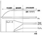
- the temperature in the epitaxial growth apparatus is raised to, for example, 1575 ° C. as a temperature raising period.
- the temperature raising period is, for example, about 40 minutes.
- pre-doping is performed in which a dopant gas containing a p-type dopant is introduced in advance.
- the p-type deep layer 5 is epitaxially grown by introducing a SiC source gas.
- SiC source gas for example, silane (SiH 4 ) as a Si source, propane (C 3 H 8 ) as a C source, or the like can be used.
- a dopant gas when forming the p-type deep layer 5 TMA (trimethylaluminum) containing a p-type dopant is used.
- hydrogen (H 2 ) is also introduced as an etching gas as necessary.
- the p-type deep layer 5 can be formed without the corner of the bottom of the deep trench 15 being made n-type. That is, the p-type dopant previously introduced at the time of pre-doping based on the Si element or C element existing by sublimation into the atmosphere or the like before the introduction of the SiC source gas, or at the initial stage when the SiC source gas is introduced SiC is crystal-grown by the incorporation of. For this reason, the p-type deep layer 5 can be formed from the corner of the bottom of the deep trench 15. Therefore, it becomes possible to accurately suppress the SiC at the corners of the deep trench 15 from becoming n-type.
- an etching gas is introduced as necessary to raise the temperature in an etching gas atmosphere, for example, a hydrogen gas atmosphere
- the etching and SiC deposition are in an equilibrium state during the temperature raising period.
- a phenomenon occurs in which SiC grows at the corners of the deep trench 15 even before the introduction of the SiC source gas.
- by performing the pre-doping of the p-type dopant it is possible to more accurately suppress the SiC at the corners of the deep trench 15 from becoming n-type.
- the impurity concentration of the p-type deep layer 5 can be appropriately controlled by controlling the pre-doping time and the amount of TMA introduced, so that the p-type deep layer 5 has a desired p-type impurity concentration. Can be formed.
- the p-type deep layer 5 is formed so as to embed the deep trench 15 using the period in which the gas ratio is stable as a steady growth period.
- the p-type impurity layer formed on the n + -type source region 4 during the formation of the p-type deep layer 5 is removed by planarization by grinding or CMP (Chemical Mechanical Polishing), and the n + -type source. The surface of region 4 is exposed. Thereby, a structure in which the p-type deep layer 5 is disposed only in the deep trench 15 is formed.
- Step shown in FIG. 2 (d) After disposing a mask material (not shown) on the surface of the n + -type source region 4 and the p-type deep layer 5, the formation planned position of the trench 6 in the mask material is opened by photolithography. Then, the trench 6 is formed in the cell region by performing anisotropic etching such as RIE with the mask material disposed. Thereafter, the mask material is removed.
- a mask material not shown
- the subsequent steps are the same as in the prior art. That is, a step of forming an interlayer insulating film, a step of forming a contact hole by photo-etching, a step of forming a source electrode 9 and a gate wiring layer by patterning after depositing an electrode material, a drain on the back surface of the n + type substrate 1 A process of forming the electrode 10 is performed. Thereby, the SiC semiconductor device in which the vertical MOSFET having the trench gate structure shown in FIG. 1 is provided in the cell region is completed.
- the p-type deep layer extends from the corner on the bottom side of the p-type deep layer 5, that is, from the corner on the bottom side of the deep trench 15. 5 is formed.
- the effect of suppressing the entry of the electric field into the trench gate structure side by the p-type deep layer 5 can be exhibited accurately. It is possible to obtain a drain-source breakdown voltage when the transistor is off.
- the p-type deep layer 5 when the p-type deep layer 5 is formed, the p-type dopant is pre-doped before introducing the SiC source gas. Thereby, the p-type deep layer 5 can be formed at the corner of the bottom of the deep trench 15 based on the Si element or C element existing by sublimation into the atmosphere or at the initial stage when the SiC source gas is introduced. . Therefore, it becomes possible to accurately suppress the SiC at the corners of the deep trench 15 from becoming n-type.
- the SiC source gas is introduced from the middle of the temperature raising period.
- the introduction amount of the SiC source gas is reduced at the initial stage of introduction, and then the introduction amount is gradually increased so as to obtain a desired introduction amount.
- the period during which the amount of SiC source gas introduced is gradually increased is the transition period, and the period after the period is constant is the steady growth period.
- the epitaxial growth is performed slowly, and a desired growth rate, for example, Epitaxial growth is performed at 4 ⁇ m / h.
- the amount of silane introduced during the transition period is gradually increased from 50 ppm to 200 ppm, and the amount of propane introduced is gradually increased from 15 ppm to 60 ppm.
- the SiC source gas by introducing the SiC source gas during the temperature rising period, it is possible to suppress the formation of step bunching on the exposed surface.
- the amount of SiC source gas introduced is gradually increased. For this reason, while suppressing the deterioration of the crystallinity of the grown crystal by suddenly increasing the amount of SiC source gas introduced during the transition period, the epitaxial growth at the desired rate is performed once the growth has progressed to such a degree that the crystallinity is unlikely to occur. Can be done.
- the flatness and crystallinity of the surface of the trench 6 are improved. it can. Therefore, the film quality of the gate insulating film 7 formed on the inner wall surface of the trench 6 can be improved, and the reliability of the gate insulating film 7 can be improved.
- a third embodiment will be described.
- the present embodiment is different from the first and second embodiments in the structure of the p-type deep layer 5 and the method of introducing the SiC source gas, and is otherwise the same as the first and second embodiments. Therefore, only different parts from the first and second embodiments will be described.
- the introduction amount of the SiC source gas is changed will be described as an example, but the introduction amount of the SiC source gas may be constant as in the first embodiment.
- angular part of the bottom part of the p-type deep layer 5 is made into the p ⁇ +> type
- the p + -type region 5a is formed below the base region 3 and away from the base region 3, but may be in a connected state.
- the p + -type region 5a has a p-type impurity concentration of, for example, 1.0 ⁇ 10 17 to 1.0 ⁇ 10 19 / cm 3 and has a triangular cross-section or a portion in contact with the p-type deep layer 5. It is a triangular round shape that is concave and curved.
- the impurity concentration of the p + -type region 5 a does not need to be constant, and the impurity concentration gradually decreases as the distance from the corner of the deep trench 15 increases to the impurity concentration of other regions in the p-type deep layer 5.
- the concentration distribution may be lowered.
- the p-type deep layer 5 has the highest p-type impurity concentration due to the formation of the p + -type region 5a at the bottom corner.
- the effect of suppressing the electric field from entering the trench gate structure side by the p-type deep layer 5 can be further exhibited. It is possible to further obtain the drain-source breakdown voltage at the off time. Further, it becomes possible to intentionally generate a breakdown in the p + type region 5a where the p-type impurity concentration is high, and to suppress the breakdown from occurring in the MOS structure portion, that is, the trench gate structure portion. it can.
- the breakdown current flows not only in the outer peripheral region but also in the cell region so that the surge current can be received over the entire surface of the substrate. Is preferable. For this reason, the breakdown current does not flow in the MOS structure portion while allowing the breakdown current to flow in the cell region, thereby improving the reliability of the vertical MOSFET and improving the withstand capability against the L load. Can also be achieved.
- the manufacturing method of the SiC semiconductor device of this embodiment is basically the same as that of the first and second embodiments, but the amount of dopant gas introduced during pre-doping is different.
- the amount of dopant gas containing a p-type dopant is increased during pre-doping than during the steady growth period. Then, when the SiC source gas starts to be introduced and the transition period starts, the amount of dopant gas introduced is reduced during that period than before the introduction of the SiC source gas. Furthermore, the amount of dopant gas introduced is gradually reduced during the transition period, and is reduced to the amount introduced during the steady growth period.
- the deep trench 15 is based on the Si element or C element present by sublimation into the atmosphere or at the initial stage when the SiC source gas is introduced.
- a p + -type region 5a can be formed at the bottom of the substrate.
- the p + -type region 5a at this time is formed with a higher impurity concentration by taking in a p-type dopant introduced in advance during pre-doping, and can be formed with a higher impurity concentration than the other regions of the p-type deep layer 5. . Since the amount of the dopant gas introduced into the pre-doping is larger than the subsequent period, the p-type impurity concentration in the p + -type region 5a can be further increased. For this reason, it becomes possible to more accurately suppress the SiC at the corners of the deep trench 15 from becoming n-type.
- the amount of dopant gas introduced is increased during the temperature rise, but thereafter the amount of dopant gas introduced is reduced. For this reason, it is possible to prevent the entire region of the p-type deep layer 5 from becoming a region having an excessively high p-type impurity concentration, and to make the entire region of the p + -type region 5a in the p-type deep layer 5 have a uniform concentration. be able to. As a result, it is possible to suppress a decrease in device breakdown voltage as in the case where the concentration distribution in other regions of the p + type region 5a in the p type deep layer 5 increases.
- the n + -type source region 4 is formed by epitaxial growth, but the n + -type source region 4 only needs to be formed in the upper layer portion of the base region 3. It can also be formed by other methods.
- the base region 3 is divided into the high-concentration base region 3a and the low-concentration base region 3b, but may be configured with a single impurity concentration. Further, in the configuration in which the impurity concentration is different, the impurity concentration gradually changes at the boundary portion between the high concentration base region 3a and the low concentration base region 3b, and the p-type impurity concentration is different across the boundary portion. 3a and the low concentration base region 3b may be stacked. Further, the low-concentration base region 3b may be constituted by an i-type semiconductor that is non-doped, that is, in a state where almost no p-type dopant is doped.
- the doping amount of the low-concentration base region 3b can be set to such an extent that the p-type dopant remaining in the atmosphere at the time of epitaxial growth is doped. In this case, it is possible to further realize a high channel mobility in the low concentration base region 3b, and to further reduce the on-resistance.
- the n ⁇ type drift layer 2 is provided on the surface of the n + type substrate 1 as a semiconductor substrate in which the back side is a back layer having a high impurity concentration and the front side is a drift layer having a lower impurity concentration.
- the structure formed is described as an example. However, this is merely an example of a semiconductor substrate.
- a high-concentration impurity layer is formed by ion-implanting an n-type dopant on the back side of the substrate constituted by the n ⁇ -type drift layer 2 or by epitaxial growth. It may be a semiconductor substrate.
- the n-channel type vertical MOSFET in which the first conductivity type is n-type and the second conductivity type is p-type has been described as an example.
- the conductivity type of each component is reversed.
- the present disclosure can also be applied to a p-channel type vertical MOSFET.
- a p-type limiting layer can be predominantly epitaxially grown on the side surface of the deep trench, and the n-type is formed at the bottom of the deep trench.
- the deep layer can be epitaxially grown predominantly.
- SiC is taken as an example of the compound semiconductor, and as an example of epitaxially growing a second conductivity type deep layer in the deep trench, a p-type deep layer is formed on the n ⁇ -type drift layer 2 serving as a base layer.
- the case of forming 5 has been described as an example. However, this is just an example. That is, for a structure in which a deep trench is formed in a first conductive type underlying layer composed of a compound semiconductor and a deep layer composed of a second conductive type compound semiconductor is epitaxially grown in the deep trench. The disclosure can be applied.
Landscapes
- Engineering & Computer Science (AREA)
- Microelectronics & Electronic Packaging (AREA)
- Condensed Matter Physics & Semiconductors (AREA)
- General Physics & Mathematics (AREA)
- Manufacturing & Machinery (AREA)
- Computer Hardware Design (AREA)
- Physics & Mathematics (AREA)
- Power Engineering (AREA)
- Chemical & Material Sciences (AREA)
- Crystallography & Structural Chemistry (AREA)
- Materials Engineering (AREA)
- Recrystallisation Techniques (AREA)
- Electrodes Of Semiconductors (AREA)
Priority Applications (1)
| Application Number | Priority Date | Filing Date | Title |
|---|---|---|---|
| US16/069,914 US10593750B2 (en) | 2016-02-23 | 2017-01-19 | Compound semiconductor device and method for manufacturing the same |
Applications Claiming Priority (2)
| Application Number | Priority Date | Filing Date | Title |
|---|---|---|---|
| JP2016032293A JP6485383B2 (ja) | 2016-02-23 | 2016-02-23 | 化合物半導体装置およびその製造方法 |
| JP2016-032293 | 2016-02-23 |
Publications (1)
| Publication Number | Publication Date |
|---|---|
| WO2017145595A1 true WO2017145595A1 (ja) | 2017-08-31 |
Family
ID=59685286
Family Applications (1)
| Application Number | Title | Priority Date | Filing Date |
|---|---|---|---|
| PCT/JP2017/001773 Ceased WO2017145595A1 (ja) | 2016-02-23 | 2017-01-19 | 化合物半導体装置およびその製造方法 |
Country Status (3)
| Country | Link |
|---|---|
| US (1) | US10593750B2 (enExample) |
| JP (1) | JP6485383B2 (enExample) |
| WO (1) | WO2017145595A1 (enExample) |
Families Citing this family (10)
| Publication number | Priority date | Publication date | Assignee | Title |
|---|---|---|---|---|
| JP6673232B2 (ja) * | 2017-01-17 | 2020-03-25 | 株式会社デンソー | 炭化珪素半導体装置 |
| JP6870547B2 (ja) * | 2017-09-18 | 2021-05-12 | 株式会社デンソー | 半導体装置およびその製造方法 |
| JP7144651B2 (ja) * | 2019-02-22 | 2022-09-30 | 豊田合成株式会社 | 半導体装置 |
| JP6773198B1 (ja) | 2019-11-06 | 2020-10-21 | 富士電機株式会社 | 炭化珪素半導体装置および炭化珪素半導体装置の製造方法 |
| JP7331783B2 (ja) * | 2020-05-29 | 2023-08-23 | 豊田合成株式会社 | 半導体装置の製造方法 |
| JP7327283B2 (ja) | 2020-05-29 | 2023-08-16 | 豊田合成株式会社 | 半導体装置 |
| JP7347335B2 (ja) * | 2020-05-29 | 2023-09-20 | 豊田合成株式会社 | 半導体装置 |
| TW202220206A (zh) * | 2020-10-12 | 2022-05-16 | 日商Flosfia股份有限公司 | 半導體裝置 |
| TW202221924A (zh) * | 2020-10-12 | 2022-06-01 | 日商Flosfia股份有限公司 | 半導體裝置 |
| CN115148826B (zh) * | 2022-09-06 | 2023-01-06 | 深圳平创半导体有限公司 | 一种深沟槽碳化硅jfet结构的制作方法 |
Citations (4)
| Publication number | Priority date | Publication date | Assignee | Title |
|---|---|---|---|---|
| JP2009302091A (ja) * | 2008-06-10 | 2009-12-24 | Denso Corp | 炭化珪素半導体装置およびその製造方法 |
| JP2013222932A (ja) * | 2012-04-19 | 2013-10-28 | Denso Corp | 炭化珪素半導体装置およびその製造方法 |
| JP2014236189A (ja) * | 2013-06-05 | 2014-12-15 | 株式会社デンソー | 炭化珪素半導体装置およびその製造方法 |
| JP2017005236A (ja) * | 2015-06-05 | 2017-01-05 | 豊田合成株式会社 | 半導体装置およびその製造方法ならびに電力変換装置 |
Family Cites Families (1)
| Publication number | Priority date | Publication date | Assignee | Title |
|---|---|---|---|---|
| JP5991809B2 (ja) * | 2011-12-07 | 2016-09-14 | ユニ・チャーム株式会社 | 使い捨て着用物品 |
-
2016
- 2016-02-23 JP JP2016032293A patent/JP6485383B2/ja not_active Expired - Fee Related
-
2017
- 2017-01-19 US US16/069,914 patent/US10593750B2/en active Active
- 2017-01-19 WO PCT/JP2017/001773 patent/WO2017145595A1/ja not_active Ceased
Patent Citations (4)
| Publication number | Priority date | Publication date | Assignee | Title |
|---|---|---|---|---|
| JP2009302091A (ja) * | 2008-06-10 | 2009-12-24 | Denso Corp | 炭化珪素半導体装置およびその製造方法 |
| JP2013222932A (ja) * | 2012-04-19 | 2013-10-28 | Denso Corp | 炭化珪素半導体装置およびその製造方法 |
| JP2014236189A (ja) * | 2013-06-05 | 2014-12-15 | 株式会社デンソー | 炭化珪素半導体装置およびその製造方法 |
| JP2017005236A (ja) * | 2015-06-05 | 2017-01-05 | 豊田合成株式会社 | 半導体装置およびその製造方法ならびに電力変換装置 |
Also Published As
| Publication number | Publication date |
|---|---|
| US20190035882A1 (en) | 2019-01-31 |
| US10593750B2 (en) | 2020-03-17 |
| JP2017152490A (ja) | 2017-08-31 |
| JP6485383B2 (ja) | 2019-03-20 |
Similar Documents
| Publication | Publication Date | Title |
|---|---|---|
| US9608104B2 (en) | Silicon carbide semiconductor device and method for manufacturing same | |
| JP6485382B2 (ja) | 化合物半導体装置の製造方法および化合物半導体装置 | |
| JP6485383B2 (ja) | 化合物半導体装置およびその製造方法 | |
| JP5717661B2 (ja) | 半導体装置とその製造方法 | |
| JP6651894B2 (ja) | 化合物半導体装置およびその製造方法 | |
| JP5298565B2 (ja) | 半導体装置およびその製造方法 | |
| US7355223B2 (en) | Vertical junction field effect transistor having an epitaxial gate | |
| US7279368B2 (en) | Method of manufacturing a vertical junction field effect transistor having an epitaxial gate | |
| JP2010147182A (ja) | エピタキシャルウエハの製造方法および半導体装置の製造方法 | |
| US9099342B2 (en) | Transistor and method for manufacturing same | |
| KR20160018322A (ko) | 반도체 장치의 제조 방법 | |
| JP2019004010A (ja) | 半導体装置およびその製造方法 | |
| US9825125B2 (en) | Silicon carbide semiconductor device and manufacturing method of silicon carbide semiconductor device | |
| JP2010103260A (ja) | 電力制御用半導体装置の製造方法 | |
| US10439037B2 (en) | Method for manufacturing compound semiconductor device including p-type impurity layer |
Legal Events
| Date | Code | Title | Description |
|---|---|---|---|
| NENP | Non-entry into the national phase |
Ref country code: DE |
|
| 121 | Ep: the epo has been informed by wipo that ep was designated in this application |
Ref document number: 17756037 Country of ref document: EP Kind code of ref document: A1 |
|
| 122 | Ep: pct application non-entry in european phase |
Ref document number: 17756037 Country of ref document: EP Kind code of ref document: A1 |