WO2017145595A1 - 化合物半導体装置およびその製造方法 - Google Patents
化合物半導体装置およびその製造方法 Download PDFInfo
- Publication number
- WO2017145595A1 WO2017145595A1 PCT/JP2017/001773 JP2017001773W WO2017145595A1 WO 2017145595 A1 WO2017145595 A1 WO 2017145595A1 JP 2017001773 W JP2017001773 W JP 2017001773W WO 2017145595 A1 WO2017145595 A1 WO 2017145595A1
- Authority
- WO
- WIPO (PCT)
- Prior art keywords
- layer
- deep
- trench
- type
- compound semiconductor
- Prior art date
Links
- 239000004065 semiconductor Substances 0.000 title claims description 70
- 150000001875 compounds Chemical class 0.000 title claims description 36
- 238000004519 manufacturing process Methods 0.000 title claims description 21
- 239000002019 doping agent Substances 0.000 claims abstract description 54
- 239000010410 layer Substances 0.000 claims description 139
- 239000012535 impurity Substances 0.000 claims description 43
- 239000000758 substrate Substances 0.000 claims description 29
- 238000005530 etching Methods 0.000 claims description 12
- 238000000034 method Methods 0.000 claims description 10
- 230000000630 rising effect Effects 0.000 claims description 5
- 239000002344 surface layer Substances 0.000 claims description 5
- JLTRXTDYQLMHGR-UHFFFAOYSA-N trimethylaluminium Chemical compound C[Al](C)C JLTRXTDYQLMHGR-UHFFFAOYSA-N 0.000 claims description 4
- 230000005684 electric field Effects 0.000 abstract description 11
- 238000010438 heat treatment Methods 0.000 abstract description 3
- 230000000149 penetrating effect Effects 0.000 abstract 1
- HBMJWWWQQXIZIP-UHFFFAOYSA-N silicon carbide Chemical compound [Si+]#[C-] HBMJWWWQQXIZIP-UHFFFAOYSA-N 0.000 description 68
- 229910010271 silicon carbide Inorganic materials 0.000 description 68
- 239000007789 gas Substances 0.000 description 57
- 230000015556 catabolic process Effects 0.000 description 19
- 239000000463 material Substances 0.000 description 10
- 230000015572 biosynthetic process Effects 0.000 description 7
- 230000000694 effects Effects 0.000 description 7
- 239000001257 hydrogen Substances 0.000 description 7
- 229910052739 hydrogen Inorganic materials 0.000 description 7
- 230000007704 transition Effects 0.000 description 7
- UFHFLCQGNIYNRP-UHFFFAOYSA-N Hydrogen Chemical compound [H][H] UFHFLCQGNIYNRP-UHFFFAOYSA-N 0.000 description 6
- 229910052751 metal Inorganic materials 0.000 description 5
- 239000002184 metal Substances 0.000 description 5
- 230000002093 peripheral effect Effects 0.000 description 5
- ATUOYWHBWRKTHZ-UHFFFAOYSA-N Propane Chemical compound CCC ATUOYWHBWRKTHZ-UHFFFAOYSA-N 0.000 description 4
- 239000013078 crystal Substances 0.000 description 4
- 230000007423 decrease Effects 0.000 description 4
- 238000000151 deposition Methods 0.000 description 3
- 239000011229 interlayer Substances 0.000 description 3
- 150000002739 metals Chemical class 0.000 description 3
- 238000001020 plasma etching Methods 0.000 description 3
- 229910021420 polycrystalline silicon Inorganic materials 0.000 description 3
- 238000000859 sublimation Methods 0.000 description 3
- 230000008022 sublimation Effects 0.000 description 3
- IJGRMHOSHXDMSA-UHFFFAOYSA-N Atomic nitrogen Chemical compound N#N IJGRMHOSHXDMSA-UHFFFAOYSA-N 0.000 description 2
- 229910002601 GaN Inorganic materials 0.000 description 2
- BLRPTPMANUNPDV-UHFFFAOYSA-N Silane Chemical compound [SiH4] BLRPTPMANUNPDV-UHFFFAOYSA-N 0.000 description 2
- 125000004429 atom Chemical group 0.000 description 2
- 230000008021 deposition Effects 0.000 description 2
- 230000006866 deterioration Effects 0.000 description 2
- 238000009826 distribution Methods 0.000 description 2
- 150000002431 hydrogen Chemical class 0.000 description 2
- 238000012986 modification Methods 0.000 description 2
- 230000004048 modification Effects 0.000 description 2
- 238000000206 photolithography Methods 0.000 description 2
- 239000001294 propane Substances 0.000 description 2
- 229910000077 silane Inorganic materials 0.000 description 2
- JMASRVWKEDWRBT-UHFFFAOYSA-N Gallium nitride Chemical compound [Ga]#N JMASRVWKEDWRBT-UHFFFAOYSA-N 0.000 description 1
- 239000000969 carrier Substances 0.000 description 1
- 239000007772 electrode material Substances 0.000 description 1
- 238000000227 grinding Methods 0.000 description 1
- 238000010348 incorporation Methods 0.000 description 1
- 229910052757 nitrogen Inorganic materials 0.000 description 1
- 125000002524 organometallic group Chemical group 0.000 description 1
- 230000003647 oxidation Effects 0.000 description 1
- 238000007254 oxidation reaction Methods 0.000 description 1
- 238000000059 patterning Methods 0.000 description 1
- 238000001259 photo etching Methods 0.000 description 1
- 238000005498 polishing Methods 0.000 description 1
- 239000002994 raw material Substances 0.000 description 1
- 238000003892 spreading Methods 0.000 description 1
- 239000000126 substance Substances 0.000 description 1
- 230000001360 synchronised effect Effects 0.000 description 1
Images

Classifications
-
- H—ELECTRICITY
- H01—ELECTRIC ELEMENTS
- H01L—SEMICONDUCTOR DEVICES NOT COVERED BY CLASS H10
- H01L29/00—Semiconductor devices adapted for rectifying, amplifying, oscillating or switching, or capacitors or resistors with at least one potential-jump barrier or surface barrier, e.g. PN junction depletion layer or carrier concentration layer; Details of semiconductor bodies or of electrodes thereof ; Multistep manufacturing processes therefor
- H01L29/02—Semiconductor bodies ; Multistep manufacturing processes therefor
- H01L29/06—Semiconductor bodies ; Multistep manufacturing processes therefor characterised by their shape; characterised by the shapes, relative sizes, or dispositions of the semiconductor regions ; characterised by the concentration or distribution of impurities within semiconductor regions
- H01L29/0603—Semiconductor bodies ; Multistep manufacturing processes therefor characterised by their shape; characterised by the shapes, relative sizes, or dispositions of the semiconductor regions ; characterised by the concentration or distribution of impurities within semiconductor regions characterised by particular constructional design considerations, e.g. for preventing surface leakage, for controlling electric field concentration or for internal isolations regions
- H01L29/0607—Semiconductor bodies ; Multistep manufacturing processes therefor characterised by their shape; characterised by the shapes, relative sizes, or dispositions of the semiconductor regions ; characterised by the concentration or distribution of impurities within semiconductor regions characterised by particular constructional design considerations, e.g. for preventing surface leakage, for controlling electric field concentration or for internal isolations regions for preventing surface leakage or controlling electric field concentration
- H01L29/0611—Semiconductor bodies ; Multistep manufacturing processes therefor characterised by their shape; characterised by the shapes, relative sizes, or dispositions of the semiconductor regions ; characterised by the concentration or distribution of impurities within semiconductor regions characterised by particular constructional design considerations, e.g. for preventing surface leakage, for controlling electric field concentration or for internal isolations regions for preventing surface leakage or controlling electric field concentration for increasing or controlling the breakdown voltage of reverse biased devices
- H01L29/0615—Semiconductor bodies ; Multistep manufacturing processes therefor characterised by their shape; characterised by the shapes, relative sizes, or dispositions of the semiconductor regions ; characterised by the concentration or distribution of impurities within semiconductor regions characterised by particular constructional design considerations, e.g. for preventing surface leakage, for controlling electric field concentration or for internal isolations regions for preventing surface leakage or controlling electric field concentration for increasing or controlling the breakdown voltage of reverse biased devices by the doping profile or the shape or the arrangement of the PN junction, or with supplementary regions, e.g. junction termination extension [JTE]
- H01L29/063—Reduced surface field [RESURF] pn-junction structures
-
- H—ELECTRICITY
- H01—ELECTRIC ELEMENTS
- H01L—SEMICONDUCTOR DEVICES NOT COVERED BY CLASS H10
- H01L21/00—Processes or apparatus adapted for the manufacture or treatment of semiconductor or solid state devices or of parts thereof
- H01L21/02—Manufacture or treatment of semiconductor devices or of parts thereof
- H01L21/02104—Forming layers
- H01L21/02365—Forming inorganic semiconducting materials on a substrate
- H01L21/02367—Substrates
- H01L21/0237—Materials
- H01L21/02373—Group 14 semiconducting materials
- H01L21/02378—Silicon carbide
-
- H—ELECTRICITY
- H01—ELECTRIC ELEMENTS
- H01L—SEMICONDUCTOR DEVICES NOT COVERED BY CLASS H10
- H01L21/00—Processes or apparatus adapted for the manufacture or treatment of semiconductor or solid state devices or of parts thereof
- H01L21/02—Manufacture or treatment of semiconductor devices or of parts thereof
- H01L21/02104—Forming layers
- H01L21/02365—Forming inorganic semiconducting materials on a substrate
- H01L21/02367—Substrates
- H01L21/02428—Structure
- H01L21/0243—Surface structure
-
- H—ELECTRICITY
- H01—ELECTRIC ELEMENTS
- H01L—SEMICONDUCTOR DEVICES NOT COVERED BY CLASS H10
- H01L21/00—Processes or apparatus adapted for the manufacture or treatment of semiconductor or solid state devices or of parts thereof
- H01L21/02—Manufacture or treatment of semiconductor devices or of parts thereof
- H01L21/02104—Forming layers
- H01L21/02365—Forming inorganic semiconducting materials on a substrate
- H01L21/02518—Deposited layers
- H01L21/02521—Materials
- H01L21/02524—Group 14 semiconducting materials
- H01L21/02529—Silicon carbide
-
- H—ELECTRICITY
- H01—ELECTRIC ELEMENTS
- H01L—SEMICONDUCTOR DEVICES NOT COVERED BY CLASS H10
- H01L21/00—Processes or apparatus adapted for the manufacture or treatment of semiconductor or solid state devices or of parts thereof
- H01L21/02—Manufacture or treatment of semiconductor devices or of parts thereof
- H01L21/02104—Forming layers
- H01L21/02365—Forming inorganic semiconducting materials on a substrate
- H01L21/02518—Deposited layers
- H01L21/0257—Doping during depositing
- H01L21/02573—Conductivity type
- H01L21/02579—P-type
-
- H—ELECTRICITY
- H01—ELECTRIC ELEMENTS
- H01L—SEMICONDUCTOR DEVICES NOT COVERED BY CLASS H10
- H01L21/00—Processes or apparatus adapted for the manufacture or treatment of semiconductor or solid state devices or of parts thereof
- H01L21/02—Manufacture or treatment of semiconductor devices or of parts thereof
- H01L21/02104—Forming layers
- H01L21/02365—Forming inorganic semiconducting materials on a substrate
- H01L21/02612—Formation types
- H01L21/02617—Deposition types
- H01L21/0262—Reduction or decomposition of gaseous compounds, e.g. CVD
-
- H—ELECTRICITY
- H01—ELECTRIC ELEMENTS
- H01L—SEMICONDUCTOR DEVICES NOT COVERED BY CLASS H10
- H01L21/00—Processes or apparatus adapted for the manufacture or treatment of semiconductor or solid state devices or of parts thereof
- H01L21/02—Manufacture or treatment of semiconductor devices or of parts thereof
- H01L21/04—Manufacture or treatment of semiconductor devices or of parts thereof the devices having at least one potential-jump barrier or surface barrier, e.g. PN junction, depletion layer or carrier concentration layer
- H01L21/0445—Manufacture or treatment of semiconductor devices or of parts thereof the devices having at least one potential-jump barrier or surface barrier, e.g. PN junction, depletion layer or carrier concentration layer the devices having semiconductor bodies comprising crystalline silicon carbide
- H01L21/0475—Changing the shape of the semiconductor body, e.g. forming recesses
-
- H—ELECTRICITY
- H01—ELECTRIC ELEMENTS
- H01L—SEMICONDUCTOR DEVICES NOT COVERED BY CLASS H10
- H01L21/00—Processes or apparatus adapted for the manufacture or treatment of semiconductor or solid state devices or of parts thereof
- H01L21/02—Manufacture or treatment of semiconductor devices or of parts thereof
- H01L21/04—Manufacture or treatment of semiconductor devices or of parts thereof the devices having at least one potential-jump barrier or surface barrier, e.g. PN junction, depletion layer or carrier concentration layer
- H01L21/0445—Manufacture or treatment of semiconductor devices or of parts thereof the devices having at least one potential-jump barrier or surface barrier, e.g. PN junction, depletion layer or carrier concentration layer the devices having semiconductor bodies comprising crystalline silicon carbide
- H01L21/048—Making electrodes
- H01L21/049—Conductor-insulator-semiconductor electrodes, e.g. MIS contacts
-
- H—ELECTRICITY
- H01—ELECTRIC ELEMENTS
- H01L—SEMICONDUCTOR DEVICES NOT COVERED BY CLASS H10
- H01L29/00—Semiconductor devices adapted for rectifying, amplifying, oscillating or switching, or capacitors or resistors with at least one potential-jump barrier or surface barrier, e.g. PN junction depletion layer or carrier concentration layer; Details of semiconductor bodies or of electrodes thereof ; Multistep manufacturing processes therefor
- H01L29/02—Semiconductor bodies ; Multistep manufacturing processes therefor
- H01L29/06—Semiconductor bodies ; Multistep manufacturing processes therefor characterised by their shape; characterised by the shapes, relative sizes, or dispositions of the semiconductor regions ; characterised by the concentration or distribution of impurities within semiconductor regions
- H01L29/10—Semiconductor bodies ; Multistep manufacturing processes therefor characterised by their shape; characterised by the shapes, relative sizes, or dispositions of the semiconductor regions ; characterised by the concentration or distribution of impurities within semiconductor regions with semiconductor regions connected to an electrode not carrying current to be rectified, amplified or switched and such electrode being part of a semiconductor device which comprises three or more electrodes
- H01L29/1095—Body region, i.e. base region, of DMOS transistors or IGBTs
-
- H—ELECTRICITY
- H01—ELECTRIC ELEMENTS
- H01L—SEMICONDUCTOR DEVICES NOT COVERED BY CLASS H10
- H01L29/00—Semiconductor devices adapted for rectifying, amplifying, oscillating or switching, or capacitors or resistors with at least one potential-jump barrier or surface barrier, e.g. PN junction depletion layer or carrier concentration layer; Details of semiconductor bodies or of electrodes thereof ; Multistep manufacturing processes therefor
- H01L29/66—Types of semiconductor device ; Multistep manufacturing processes therefor
- H01L29/66007—Multistep manufacturing processes
- H01L29/66053—Multistep manufacturing processes of devices having a semiconductor body comprising crystalline silicon carbide
- H01L29/66068—Multistep manufacturing processes of devices having a semiconductor body comprising crystalline silicon carbide the devices being controllable only by the electric current supplied or the electric potential applied, to an electrode which does not carry the current to be rectified, amplified or switched, e.g. three-terminal devices
-
- H—ELECTRICITY
- H01—ELECTRIC ELEMENTS
- H01L—SEMICONDUCTOR DEVICES NOT COVERED BY CLASS H10
- H01L29/00—Semiconductor devices adapted for rectifying, amplifying, oscillating or switching, or capacitors or resistors with at least one potential-jump barrier or surface barrier, e.g. PN junction depletion layer or carrier concentration layer; Details of semiconductor bodies or of electrodes thereof ; Multistep manufacturing processes therefor
- H01L29/66—Types of semiconductor device ; Multistep manufacturing processes therefor
- H01L29/68—Types of semiconductor device ; Multistep manufacturing processes therefor controllable by only the electric current supplied, or only the electric potential applied, to an electrode which does not carry the current to be rectified, amplified or switched
- H01L29/76—Unipolar devices, e.g. field effect transistors
- H01L29/772—Field effect transistors
- H01L29/78—Field effect transistors with field effect produced by an insulated gate
- H01L29/7801—DMOS transistors, i.e. MISFETs with a channel accommodating body or base region adjoining a drain drift region
- H01L29/7802—Vertical DMOS transistors, i.e. VDMOS transistors
- H01L29/7813—Vertical DMOS transistors, i.e. VDMOS transistors with trench gate electrode, e.g. UMOS transistors
-
- H—ELECTRICITY
- H01—ELECTRIC ELEMENTS
- H01L—SEMICONDUCTOR DEVICES NOT COVERED BY CLASS H10
- H01L29/00—Semiconductor devices adapted for rectifying, amplifying, oscillating or switching, or capacitors or resistors with at least one potential-jump barrier or surface barrier, e.g. PN junction depletion layer or carrier concentration layer; Details of semiconductor bodies or of electrodes thereof ; Multistep manufacturing processes therefor
- H01L29/02—Semiconductor bodies ; Multistep manufacturing processes therefor
- H01L29/12—Semiconductor bodies ; Multistep manufacturing processes therefor characterised by the materials of which they are formed
- H01L29/16—Semiconductor bodies ; Multistep manufacturing processes therefor characterised by the materials of which they are formed including, apart from doping materials or other impurities, only elements of Group IV of the Periodic System
- H01L29/1608—Silicon carbide
-
- H—ELECTRICITY
- H01—ELECTRIC ELEMENTS
- H01L—SEMICONDUCTOR DEVICES NOT COVERED BY CLASS H10
- H01L29/00—Semiconductor devices adapted for rectifying, amplifying, oscillating or switching, or capacitors or resistors with at least one potential-jump barrier or surface barrier, e.g. PN junction depletion layer or carrier concentration layer; Details of semiconductor bodies or of electrodes thereof ; Multistep manufacturing processes therefor
- H01L29/02—Semiconductor bodies ; Multistep manufacturing processes therefor
- H01L29/12—Semiconductor bodies ; Multistep manufacturing processes therefor characterised by the materials of which they are formed
- H01L29/20—Semiconductor bodies ; Multistep manufacturing processes therefor characterised by the materials of which they are formed including, apart from doping materials or other impurities, only AIIIBV compounds
- H01L29/2003—Nitride compounds
Definitions
- the present disclosure relates to a method of manufacturing a compound semiconductor device and a compound semiconductor device using a compound semiconductor such as silicon carbide (hereinafter referred to as SiC) or gallium nitride (hereinafter referred to as GaN).
- a compound semiconductor such as silicon carbide (hereinafter referred to as SiC) or gallium nitride (hereinafter referred to as GaN).
- Patent Document 1 proposes an SiC semiconductor device including a vertical MOSFET having an inverted trench gate structure as a vertical switching element having a trench gate structure.
- a gate voltage is applied to the gate electrode in the gate trench to form a channel in the p-type base region located on the side surface of the gate trench, and the drain / Current flows between sources.
- a vertical MOSFET having a trench gate structure when a high electric field is applied to the gate insulating film provided in the trench gate structure, dielectric breakdown occurs and the device breakdown voltage decreases.
- the process window of the growth condition is narrow, and the corner of the bottom of the deep trench may become n-type.
- the p-type deep layer does not provide a sufficient effect of suppressing the entry of the electric field to the trench gate structure side, and the drain-source breakdown voltage at the time of OFF is low. It can no longer be obtained.
- n-type dopant atoms for example, nitrogen
- the SiC raw material it is possible to prevent the bottom corners of the deep trench from becoming n-type, but it is difficult to prepare the high-purity material and the cost is increased.
- the p-type deep layer may be epitaxially grown in a high-temperature hydrogen atmosphere, but etching by hydrogen or high temperature and SiC deposition are in an equilibrium state, and SiC is formed at the corners of the deep trench even before the introduction of the SiC source gas. The phenomenon of crystal growth occurs.
- a semiconductor substrate having a first conductivity type underlayer composed of a compound semiconductor is prepared, and a deep trench is formed in the underlayer. And introducing a dopant gas containing a second conductivity type dopant into the epitaxial growth apparatus, introducing a compound semiconductor source gas, and epitaxially growing a second conductivity type deep layer in the deep trench.
- the temperature raising period of the epitaxial growth apparatus is set to a temperature raising period to a temperature at which the deep layer is epitaxially grown, and after the introduction of the dopant gas containing the second conductivity type dopant from the temperature raising period, A deep layer is also formed at the corner of the bottom of the deep trench by introducing the source gas later. Formation to.
- the source gas is introduced after the temperature raising period.
- a deep layer can be formed from the corner
- a method of manufacturing a compound semiconductor device includes providing a semiconductor substrate having a first conductivity type base layer made of a compound semiconductor, and forming a deep trench in the base layer. And introducing a source gas of a compound semiconductor while introducing a dopant gas containing a second conductivity type dopant in the epitaxial growth apparatus, and epitaxially growing a second conductivity type deep layer in the deep trench, In forming the deep layer, the temperature of the epitaxial growth apparatus is raised to a temperature at which the deep layer is epitaxially grown, and the temperature is raised after introducing a dopant gas containing a second conductivity type dopant from the temperature raising period. By introducing the source gas after the introduction of the dopant gas during the period, deep also form a deep layer on the bottom corner of the wrench.
- the source gas may be introduced after the dopant gas is introduced during the temperature rising period.
- the deep layer can be formed from the corner, that is, the corner on the bottom side of the deep trench. Therefore, the effect of suppressing the entry of the electric field to the trench gate structure side by the deep layer can be exhibited accurately. It is possible to obtain a drain-source breakdown voltage when the transistor is off.
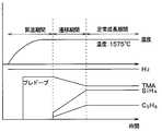
- FIG. 3 is a cross-sectional view showing a manufacturing process of the SiC semiconductor device shown in FIG. 1. It is the time chart which showed the growth program of the p-type deep layer in the deep trench concerning 1st Embodiment. It is the time chart which showed the growth program of the p-type deep layer in the deep trench concerning 2nd Embodiment. It is sectional drawing of the SiC semiconductor device provided with the vertical MOSFET concerning 3rd Embodiment. It is the time chart which showed the growth program of the p-type deep layer in the deep trench concerning 3rd Embodiment.
- the SiC semiconductor device shown in FIG. 1 has a structure in which a vertical MOSFET having a trench gate structure is formed in a cell region, and an outer peripheral breakdown voltage structure is provided in an outer peripheral region surrounding the cell region.
- the SiC semiconductor device is a semiconductor in which an n ⁇ type drift layer 2 made of SiC having a lower impurity concentration than the n + type substrate 1 is formed on the surface side of the n + type substrate 1 constituting the high concentration impurity layer made of SiC. It is formed using a substrate.
- the n + type substrate 1 has, for example, an n type impurity concentration of 1.0 ⁇ 10 19 / cm 3 and a surface that is a (0001) Si surface.
- the n ⁇ type drift layer 2 has an n type impurity concentration of 0.5 to 2.0 ⁇ 10 16 / cm 3 .
- Base region 3 is formed in the upper layer portion of n ⁇ type drift layer 2.
- the base region 3 is composed of p-type SiC having a higher impurity concentration than the n ⁇ -type drift layer 2, and a high-concentration base region 3 a having a relatively high p-type impurity concentration,
- a low-concentration base region 3b having a lower p-type impurity concentration is sequentially stacked.
- the high concentration base region 3a has, for example, a p-type impurity concentration of 5 ⁇ 10 17 / cm 3 or more, for example, 1 ⁇ 10 18 / cm 3, and a thickness of 50 to 200 nm.
- the low concentration base region 3b has, for example, a p-type impurity concentration of 1.0 ⁇ 10 16 / cm 3 or less and a thickness of 0.2 to 1.0 ⁇ m.
- an n + type source region 4 is formed in the upper layer portion of the base region 3. Further, through the n + -type source region n + -type source region 4 and the base region 3 from the surface of the 4, n - p-type deep layer 5 is formed so as to reach the type drift layer 2. Specifically, the n + -type source region 4 and the base region 3 through the surface of the n + -type source region 4, n - -type drift layer 2 deep trench 15 reaching are formed, the deep trench 15 The p-type deep layer 5 is embedded in For example, the deep trench 15 has an aspect ratio of 2 or more.
- the n + type source regions 4 are arranged on both sides of a trench gate structure described later.
- the p-type deep layer 5 is formed to a position deeper than the trench gate structure on the opposite side of the trench gate structure with the n + -type source region 4 interposed therebetween, and is embedded up to the corner at the bottom of the deep trench 15. That is, the corner of the bottom of the deep trench 15 is not n-type, and the deep trench 15 is embedded with the p-type deep layer 5.
- the n + -type source region 4 has an n-type impurity concentration in the surface layer portion of, for example, 2.5 ⁇ 10 18 to 1.0 ⁇ 10 19 / cm 3 and a thickness of about 0.5 ⁇ m.
- the p-type deep layer 5 has a higher impurity concentration than that of the base region 3, and the p-type impurity concentration is, for example, 1.0 ⁇ 10 17 to 1.0 ⁇ 10 19 / cm 3 .
- the p-type deep layer 5 also serves as a contact region in which electrical connection is made with a source electrode 9 described later.
- a trench 6 having a longitudinal direction in the plane of the drawing as a longitudinal direction is formed so as to penetrate the base region 3 and the n + type source region 4 and reach the n ⁇ type drift layer 2.
- the high-concentration base region 3a, the low-concentration base region 3b, and the n + -type source region 4 in the base region 3 are arranged so as to be in contact with the side surface of the trench 6.
- a surface layer portion of the base region 3 located between the n + type source region 4 and the n ⁇ type drift layer 2 is used as a channel region, and a gate insulating film is formed on the inner wall surface of the trench 6 including the channel region. 7 is formed.
- a gate electrode 8 made of doped Poly-Si is formed on the surface of the gate insulating film 7, and the trench 6 is filled with the gate insulating film 7 and the gate electrode 8.
- a trench gate structure is configured.
- This trench gate structure is extended with the vertical direction in FIG. 1 as the longitudinal direction, and a plurality of trench gate structures are arranged in the left-right direction in FIG. 1 to form a stripe shape.
- the n + -type source region 4 and the p-type deep layer 5 described above also have a layout structure extending along the longitudinal direction of the trench gate structure.
- a source electrode 9 and a gate wiring are formed on the surface of the n + type source region 4 and the p type deep layer 5 and the surface of the gate electrode 8.
- the source electrode 9 and the gate wiring are made of a plurality of metals such as Ni / Al.
- the plurality of metals at least the n-type SiC, specifically, the n + -type source region 4 or the portion in contact with the gate electrode 8 in the case of n-type doping is made of a metal capable of ohmic contact with the n-type SiC. Yes.
- the plurality of metals that contacts the p-type SiC is made of a metal that can make ohmic contact with the p-type SiC.
- the source electrode 9 and the gate wiring are electrically insulated by being formed on an interlayer insulating film (not shown).
- the source electrode 9 is in electrical contact with the n + type source region 4 and the p type deep layer 5 through the contact hole formed in the interlayer insulating film, and the gate wiring is in electrical contact with the gate electrode 8. ing.
- n + -type substrate 1 electrically connected to a drain electrode 10 are formed.
- an n-channel type inverted MOSFET having a trench gate structure is formed.
- the SiC semiconductor device concerning this embodiment is comprised by providing the outer peripheral pressure
- the corners of the deep trench 15 are buried with the p-type deep layer 5 so that the n-type layer is not formed in the corner of the deep trench 15. I have to.
- the base region 3 is constituted by the high concentration base region 3a and the low concentration base region 3b, and a channel is formed by the high concentration base region 3a and the low concentration base region 3b. .
- the high concentration base region 3a spreading of the depletion layer in the base region 3 can be suppressed by the high concentration base region 3a. Therefore, it is possible to prevent the base region 3 from being completely depleted and punch-through, to ensure the element breakdown voltage, and to prevent the gate insulating film 7 at the bottom of the trench 6 from being deteriorated.
- the threshold voltage depends on the p-type impurity concentration of the high-concentration base region 3a, it is possible to obtain a high threshold voltage.
- the channel mobility is increased in the portion of the low concentration base region 3b, even if the high concentration base region 3a is provided, the on-resistance can be reduced. Therefore, it is possible to obtain a vertical MOSFET having a trench gate structure that can reduce the on-resistance and ensure the element withstand voltage and obtain a high threshold voltage.
- the presence of the high concentration base region 3a enhances the effect of extracting carriers generated from the junction between the n ⁇ -type drift layer 2 and the base region 3 at the time of off, so that the drain leakage current can be reduced.
- the base region 3 that are in contact with the n ⁇ type drift layer 2 are high concentration base regions 3a having a high p type impurity concentration, the PN between the n ⁇ type drift layer 2 and the base region 3 The rising voltage when a current flows through the built-in diode formed by the junction can be reduced. For this reason, the on-voltage of the built-in diode is reduced, and it is possible to reduce the loss during the synchronous rectification drive using the built-in diode positively.
- the depletion layer extending from the high-concentration base region 3a side to the n ⁇ -type drift layer 2 side can prevent the equipotential lines from entering below the trench gate structure. For this reason, the electric field concentration applied to the gate insulating film 7 on the bottom surface of the trench 6 can be relaxed, and the life of the gate insulating film 7 and the reverse bias life can be improved.
- a so-called epi substrate in which an n ⁇ type drift layer 2 made of SiC is epitaxially grown on the surface of an n + type substrate 1 made of SiC is prepared. Then, this epi substrate is placed in an epitaxial growth apparatus, and a high concentration base region 3a, a low concentration base region 3b, and an n + type source region 4 are epitaxially grown on the surface of the n ⁇ type drift layer 2 in this order.
- Step shown in FIG. 2 (b) After a mask material (not shown) is arranged on the surface of the n + -type source region 4, a planned formation position of the p-type deep layer 5 in the mask material is opened by photolithography. Then, anisotropic etching such as RIE (Reactive Ion Etching) is performed in a state where the mask material is arranged, thereby forming the deep trench 15 at a position where the p-type deep layer 5 is to be formed.
- RIE Reactive Ion Etching
- Step shown in FIG. 2 (c) The process of forming the p-type deep layer 5 is continuously performed using an epitaxial growth apparatus (not shown).
- the temperature in the epitaxial growth apparatus is raised to, for example, 1575 ° C. as a temperature raising period.
- the temperature raising period is, for example, about 40 minutes.
- pre-doping is performed in which a dopant gas containing a p-type dopant is introduced in advance.
- the p-type deep layer 5 is epitaxially grown by introducing a SiC source gas.
- SiC source gas for example, silane (SiH 4 ) as a Si source, propane (C 3 H 8 ) as a C source, or the like can be used.
- a dopant gas when forming the p-type deep layer 5 TMA (trimethylaluminum) containing a p-type dopant is used.
- hydrogen (H 2 ) is also introduced as an etching gas as necessary.
- the p-type deep layer 5 can be formed without the corner of the bottom of the deep trench 15 being made n-type. That is, the p-type dopant previously introduced at the time of pre-doping based on the Si element or C element existing by sublimation into the atmosphere or the like before the introduction of the SiC source gas, or at the initial stage when the SiC source gas is introduced SiC is crystal-grown by the incorporation of. For this reason, the p-type deep layer 5 can be formed from the corner of the bottom of the deep trench 15. Therefore, it becomes possible to accurately suppress the SiC at the corners of the deep trench 15 from becoming n-type.
- an etching gas is introduced as necessary to raise the temperature in an etching gas atmosphere, for example, a hydrogen gas atmosphere
- the etching and SiC deposition are in an equilibrium state during the temperature raising period.
- a phenomenon occurs in which SiC grows at the corners of the deep trench 15 even before the introduction of the SiC source gas.
- by performing the pre-doping of the p-type dopant it is possible to more accurately suppress the SiC at the corners of the deep trench 15 from becoming n-type.
- the impurity concentration of the p-type deep layer 5 can be appropriately controlled by controlling the pre-doping time and the amount of TMA introduced, so that the p-type deep layer 5 has a desired p-type impurity concentration. Can be formed.
- the p-type deep layer 5 is formed so as to embed the deep trench 15 using the period in which the gas ratio is stable as a steady growth period.
- the p-type impurity layer formed on the n + -type source region 4 during the formation of the p-type deep layer 5 is removed by planarization by grinding or CMP (Chemical Mechanical Polishing), and the n + -type source. The surface of region 4 is exposed. Thereby, a structure in which the p-type deep layer 5 is disposed only in the deep trench 15 is formed.
- Step shown in FIG. 2 (d) After disposing a mask material (not shown) on the surface of the n + -type source region 4 and the p-type deep layer 5, the formation planned position of the trench 6 in the mask material is opened by photolithography. Then, the trench 6 is formed in the cell region by performing anisotropic etching such as RIE with the mask material disposed. Thereafter, the mask material is removed.
- a mask material not shown
- the subsequent steps are the same as in the prior art. That is, a step of forming an interlayer insulating film, a step of forming a contact hole by photo-etching, a step of forming a source electrode 9 and a gate wiring layer by patterning after depositing an electrode material, a drain on the back surface of the n + type substrate 1 A process of forming the electrode 10 is performed. Thereby, the SiC semiconductor device in which the vertical MOSFET having the trench gate structure shown in FIG. 1 is provided in the cell region is completed.
- the p-type deep layer extends from the corner on the bottom side of the p-type deep layer 5, that is, from the corner on the bottom side of the deep trench 15. 5 is formed.
- the effect of suppressing the entry of the electric field into the trench gate structure side by the p-type deep layer 5 can be exhibited accurately. It is possible to obtain a drain-source breakdown voltage when the transistor is off.
- the p-type deep layer 5 when the p-type deep layer 5 is formed, the p-type dopant is pre-doped before introducing the SiC source gas. Thereby, the p-type deep layer 5 can be formed at the corner of the bottom of the deep trench 15 based on the Si element or C element existing by sublimation into the atmosphere or at the initial stage when the SiC source gas is introduced. . Therefore, it becomes possible to accurately suppress the SiC at the corners of the deep trench 15 from becoming n-type.
- the SiC source gas is introduced from the middle of the temperature raising period.
- the introduction amount of the SiC source gas is reduced at the initial stage of introduction, and then the introduction amount is gradually increased so as to obtain a desired introduction amount.
- the period during which the amount of SiC source gas introduced is gradually increased is the transition period, and the period after the period is constant is the steady growth period.
- the epitaxial growth is performed slowly, and a desired growth rate, for example, Epitaxial growth is performed at 4 ⁇ m / h.
- the amount of silane introduced during the transition period is gradually increased from 50 ppm to 200 ppm, and the amount of propane introduced is gradually increased from 15 ppm to 60 ppm.
- the SiC source gas by introducing the SiC source gas during the temperature rising period, it is possible to suppress the formation of step bunching on the exposed surface.
- the amount of SiC source gas introduced is gradually increased. For this reason, while suppressing the deterioration of the crystallinity of the grown crystal by suddenly increasing the amount of SiC source gas introduced during the transition period, the epitaxial growth at the desired rate is performed once the growth has progressed to such a degree that the crystallinity is unlikely to occur. Can be done.
- the flatness and crystallinity of the surface of the trench 6 are improved. it can. Therefore, the film quality of the gate insulating film 7 formed on the inner wall surface of the trench 6 can be improved, and the reliability of the gate insulating film 7 can be improved.
- a third embodiment will be described.
- the present embodiment is different from the first and second embodiments in the structure of the p-type deep layer 5 and the method of introducing the SiC source gas, and is otherwise the same as the first and second embodiments. Therefore, only different parts from the first and second embodiments will be described.
- the introduction amount of the SiC source gas is changed will be described as an example, but the introduction amount of the SiC source gas may be constant as in the first embodiment.
- angular part of the bottom part of the p-type deep layer 5 is made into the p ⁇ +> type
- the p + -type region 5a is formed below the base region 3 and away from the base region 3, but may be in a connected state.
- the p + -type region 5a has a p-type impurity concentration of, for example, 1.0 ⁇ 10 17 to 1.0 ⁇ 10 19 / cm 3 and has a triangular cross-section or a portion in contact with the p-type deep layer 5. It is a triangular round shape that is concave and curved.
- the impurity concentration of the p + -type region 5 a does not need to be constant, and the impurity concentration gradually decreases as the distance from the corner of the deep trench 15 increases to the impurity concentration of other regions in the p-type deep layer 5.
- the concentration distribution may be lowered.
- the p-type deep layer 5 has the highest p-type impurity concentration due to the formation of the p + -type region 5a at the bottom corner.
- the effect of suppressing the electric field from entering the trench gate structure side by the p-type deep layer 5 can be further exhibited. It is possible to further obtain the drain-source breakdown voltage at the off time. Further, it becomes possible to intentionally generate a breakdown in the p + type region 5a where the p-type impurity concentration is high, and to suppress the breakdown from occurring in the MOS structure portion, that is, the trench gate structure portion. it can.
- the breakdown current flows not only in the outer peripheral region but also in the cell region so that the surge current can be received over the entire surface of the substrate. Is preferable. For this reason, the breakdown current does not flow in the MOS structure portion while allowing the breakdown current to flow in the cell region, thereby improving the reliability of the vertical MOSFET and improving the withstand capability against the L load. Can also be achieved.
- the manufacturing method of the SiC semiconductor device of this embodiment is basically the same as that of the first and second embodiments, but the amount of dopant gas introduced during pre-doping is different.
- the amount of dopant gas containing a p-type dopant is increased during pre-doping than during the steady growth period. Then, when the SiC source gas starts to be introduced and the transition period starts, the amount of dopant gas introduced is reduced during that period than before the introduction of the SiC source gas. Furthermore, the amount of dopant gas introduced is gradually reduced during the transition period, and is reduced to the amount introduced during the steady growth period.
- the deep trench 15 is based on the Si element or C element present by sublimation into the atmosphere or at the initial stage when the SiC source gas is introduced.
- a p + -type region 5a can be formed at the bottom of the substrate.
- the p + -type region 5a at this time is formed with a higher impurity concentration by taking in a p-type dopant introduced in advance during pre-doping, and can be formed with a higher impurity concentration than the other regions of the p-type deep layer 5. . Since the amount of the dopant gas introduced into the pre-doping is larger than the subsequent period, the p-type impurity concentration in the p + -type region 5a can be further increased. For this reason, it becomes possible to more accurately suppress the SiC at the corners of the deep trench 15 from becoming n-type.
- the amount of dopant gas introduced is increased during the temperature rise, but thereafter the amount of dopant gas introduced is reduced. For this reason, it is possible to prevent the entire region of the p-type deep layer 5 from becoming a region having an excessively high p-type impurity concentration, and to make the entire region of the p + -type region 5a in the p-type deep layer 5 have a uniform concentration. be able to. As a result, it is possible to suppress a decrease in device breakdown voltage as in the case where the concentration distribution in other regions of the p + type region 5a in the p type deep layer 5 increases.
- the n + -type source region 4 is formed by epitaxial growth, but the n + -type source region 4 only needs to be formed in the upper layer portion of the base region 3. It can also be formed by other methods.
- the base region 3 is divided into the high-concentration base region 3a and the low-concentration base region 3b, but may be configured with a single impurity concentration. Further, in the configuration in which the impurity concentration is different, the impurity concentration gradually changes at the boundary portion between the high concentration base region 3a and the low concentration base region 3b, and the p-type impurity concentration is different across the boundary portion. 3a and the low concentration base region 3b may be stacked. Further, the low-concentration base region 3b may be constituted by an i-type semiconductor that is non-doped, that is, in a state where almost no p-type dopant is doped.
- the doping amount of the low-concentration base region 3b can be set to such an extent that the p-type dopant remaining in the atmosphere at the time of epitaxial growth is doped. In this case, it is possible to further realize a high channel mobility in the low concentration base region 3b, and to further reduce the on-resistance.
- the n ⁇ type drift layer 2 is provided on the surface of the n + type substrate 1 as a semiconductor substrate in which the back side is a back layer having a high impurity concentration and the front side is a drift layer having a lower impurity concentration.
- the structure formed is described as an example. However, this is merely an example of a semiconductor substrate.
- a high-concentration impurity layer is formed by ion-implanting an n-type dopant on the back side of the substrate constituted by the n ⁇ -type drift layer 2 or by epitaxial growth. It may be a semiconductor substrate.
- the n-channel type vertical MOSFET in which the first conductivity type is n-type and the second conductivity type is p-type has been described as an example.
- the conductivity type of each component is reversed.
- the present disclosure can also be applied to a p-channel type vertical MOSFET.
- a p-type limiting layer can be predominantly epitaxially grown on the side surface of the deep trench, and the n-type is formed at the bottom of the deep trench.
- the deep layer can be epitaxially grown predominantly.
- SiC is taken as an example of the compound semiconductor, and as an example of epitaxially growing a second conductivity type deep layer in the deep trench, a p-type deep layer is formed on the n ⁇ -type drift layer 2 serving as a base layer.
- the case of forming 5 has been described as an example. However, this is just an example. That is, for a structure in which a deep trench is formed in a first conductive type underlying layer composed of a compound semiconductor and a deep layer composed of a second conductive type compound semiconductor is epitaxially grown in the deep trench. The disclosure can be applied.
Abstract
p型ディープ層(5)の底部側の角部、つまりディープトレンチ(15)における底部側の角部からp型ディープ層(5)が形成されるようにする。すなわち、ディープトレンチ(15)の底部の角部がn型化することを抑制する。例えば、p型ディープ層(5)をエピタキシャル成長させる温度までエピタキシャル成長装置を昇温させる期間を昇温期間として、昇温期間中からp型ドーパントを含むドーパントガスを導入したのち、昇温期間後に原料ガスを導入する。これにより、ディープトレンチ(15)の底部の角部にもp型ディープ層(5)を形成できる。したがって、p型ディープ層(5)によるトレンチゲート構造側への電界の入り込み抑制効果を的確に発揮させることが可能となり。オフ時におけるドレイン-ソース間耐圧を得ることができる。
Description
本出願は、2016年2月23日に出願された日本特許出願番号2016-32293号に基づくもので、ここにその記載内容が参照により組み入れられる。
本開示は、例えば炭化珪素(以下、SiCという)や窒化ガリウム(以下、GaNという)などの化合物半導体を用いた化合物半導体装置の製造方法および化合物半導体装置に関する。
従来、特許文献1に、トレンチゲート構造の縦型スイッチング素子として、反転型のトレンチゲート構造の縦型MOSFETを備えたSiC半導体装置が提案されている。反転型のトレンチゲート構造の縦型MOSFETでは、ゲートトレンチ内のゲート電極に対してゲート電圧を印加することで、ゲートトレンチ側面に位置するp型ベース領域にチャネルを形成し、このチャネルを通じてドレイン・ソース間に電流を流す。このようなトレンチゲート構造の縦型MOSFETでは、トレンチゲート構造に備えられるゲート絶縁膜に対して高電界が加わると絶縁破壊が生じて素子耐圧が低下してしまう。
このため、特許文献1に記載のSiC半導体装置では、トレンチゲート構造を挟んだ両側に、n+型ソース領域およびp型ベース領域を貫通してn-型ドリフト層に達するディープトレンチを形成し、このトレンチ内にp型ディープ層を備えるようにしている。このようなp型ディープ層を備えることで電界がゲート絶縁膜に入り込むことを抑制でき、ゲート絶縁膜を高電界から保護できる。したがって、ゲート絶縁膜の絶縁破壊が起こり難くなり、素子耐圧を向上することが可能となる。
エピタキシャル成長によってディープトレンチ内に均一濃度でp型ディープ層を形成しようとすると、成長条件のプロセスウィンドウが狭く、ディープトレンチの底部の角部がn型化することがあった。このように、ディープトレンチの底部の角部がn型化した場合、p型ディープ層によるトレンチゲート構造側への電界の入り込み抑制効果が十分に得られず、オフ時におけるドレイン-ソース間耐圧が得られなくなる。
例えば、表面がSi面となるSiC基板を用いた場合、ディープトレンチの角部に相当する部分の結晶面方位においてn型ドーパント原子(例えば窒素)が取り込まれ易い。このため、エピタキシャル成長装置内やSiC原料ガスに含まれる微量のn型ドーパント原子が取り込まれてディープトレンチの底部の角部がn型化することがあると考えられる。SiC原料として高純度材料を用いれば、ディープトレンチの底部の角部がn型化することを抑制できるが、高純度材料を準備することが難しく、コスト高にもなる。また、高温水素雰囲気においてp型ディープ層をエピタキシャル成長させるようにしても良いが、水素や高温によるエッチングとSiCのデポジションとが平衡状態となり、SiC原料ガス導入前でもディープトレンチの角部にSiCが結晶成長する現象が起こる。
本開示は、ドレイン-ソース間の耐圧の低下を抑制できる化合物半導体装置の製造方法および化合物半導体装置を提供することを目的とする。
本開示の1つの観点における化合物半導体装置の製造方法では、化合物半導体にて構成される第1導電型の下地層を有する半導体基板を用意することと、下地層に対してディープトレンチを形成することと、エピタキシャル成長装置内に第2導電型ドーパントを含むドーパントガスを導入しつつ、化合物半導体の原料ガスを導入し、ディープトレンチ内に第2導電型のディープ層をエピタキシャル成長させることと、を含み、ディープ層を形成することでは、ディープ層をエピタキシャル成長させる温度までエピタキシャル成長装置を昇温させる期間を昇温期間として、該昇温期間中から第2導電型ドーパントを含むドーパントガスを導入したのち、昇温期間後に原料ガスを導入することで、ディープトレンチの底部の角部にもディープ層を形成する。
このように、昇温期間中から第2導電型ドーパントを含むドーパントガスを導入したのち、昇温期間後に原料ガスを導入している。これにより、ディープ層の底部側の角部、つまりディープトレンチにおける底部側の角部からディープ層が形成されるようにできる。したがって、ディープ層によるトレンチゲート構造側への電界の入り込み抑制効果を的確に発揮させることが可能となり。オフ時におけるドレイン-ソース間耐圧を得ることができる。
本開示のもう1つの観点における化合物半導体装置の製造方法では、化合物半導体にて構成される第1導電型の下地層を有する半導体基板を用意することと、下地層に対してディープトレンチを形成することと、エピタキシャル成長装置内に第2導電型ドーパントを含むドーパントガスを導入しつつ、化合物半導体の原料ガスを導入し、ディープトレンチ内に第2導電型のディープ層をエピタキシャル成長させることと、を含み、ディープ層を形成することでは、ディープ層をエピタキシャル成長させる温度までエピタキシャル成長装置を昇温させる期間を昇温期間として、該昇温期間中から第2導電型ドーパントを含むドーパントガスを導入したのち、昇温期間中におけるドーパントガスの導入後に原料ガスを導入することで、ディープトレンチの底部の角部にもディープ層を形成する。
このように、昇温期間中から第2導電型ドーパントを含むドーパントガスを導入したのち、昇温期間中におけるドーパントガスの導入後に原料ガスを導入するようにしても、ディープ層の底部側の角部、つまりディープトレンチにおける底部側の角部からディープ層が形成されるようにできる。したがって、ディープ層によるトレンチゲート構造側への電界の入り込み抑制効果を的確に発揮させることが可能となり。オフ時におけるドレイン-ソース間耐圧を得ることができる。
以下、本開示の実施形態について図に基づいて説明する。なお、以下の各実施形態相互において、互いに同一もしくは均等である部分には、同一符号を付して説明を行う。
(第1実施形態)
本実施形態にかかるトレンチゲート構造の反転型の縦型MOSFETが形成されたSiC半導体装置について、図1を参照して説明する。
本実施形態にかかるトレンチゲート構造の反転型の縦型MOSFETが形成されたSiC半導体装置について、図1を参照して説明する。
図1に示すSiC半導体装置は、セル領域にトレンチゲート構造の縦型MOSFETが形成され、図示していないが、セル領域を囲む外周領域に外周耐圧構造が備えられた構成とされている。
SiC半導体装置は、SiCからなる高濃度不純物層を構成するn+型基板1の表面側に、n+型基板1よりも低不純物濃度のSiCからなるn-型ドリフト層2が形成された半導体基板を用いて形成されている。n+型基板1は、例えばn型不純物濃度が1.0×10¹⁹/cm3とされ、表面が(0001)Si面とされている。n-型ドリフト層2は、例えばn型不純物濃度が0.5~2.0×1016/cm3とされている。
n-型ドリフト層2の上層部にはベース領域3が形成されている。本実施形態の場合、ベース領域3は、n-型ドリフト層2よりも高不純物濃度のp型SiCで構成されており、p型不純物濃度が比較的高くされた高濃度ベース領域3aと、それよりもp型不純物濃度が低くされた低濃度ベース領域3bとが順に積層された構造とされている。
高濃度ベース領域3aは、例えばp型不純物濃度が5×10¹⁷/cm3以上、例えば1×1018/cm3とされ、厚みが50~200nmとされている。低濃度ベース領域3bは、例えばp型不純物濃度が1.0×1016/cm3以下とされ、厚みが0.2~1.0μmとされている。
さらに、ベース領域3の上層部分にはn+型ソース領域4が形成されている。また、n+型ソース領域4の表面からn+型ソース領域4およびベース領域3を貫通し、n-型ドリフト層2に達するようにp型ディープ層5が形成されている。具体的には、n+型ソース領域4の表面からn+型ソース領域4およびベース領域3を貫通し、n-型ドリフト層2に達するディープトレンチ15が形成されており、このディープトレンチ15内にp型ディープ層5が埋め込まれている。例えば、ディープトレンチ15は、アスペクト比が2以上の深さとされている。
n+型ソース領域4は、後述するトレンチゲート構造の両側に配置されている。p型ディープ層5は、n+型ソース領域4を挟んでトレンチゲート構造と反対側においてトレンチゲート構造よりも深い位置まで形成されており、ディープトレンチ15の底部の角部まで埋め込まれている。すなわち、ディープトレンチ15の底部の角部がn型化されておらず、ディープトレンチ15内がp型ディープ層5で埋め込まれた構造とされている。n+型ソース領域4は、表層部におけるn型不純物濃度が例えば2.5×10¹⁸~1.0×10¹⁹/cm3、厚さ0.5μm程度で構成されている。また、p型ディープ層5は、ベース領域3よりも高不純物濃度とされ、p型不純物濃度が例えば1.0×1017~1.0×1019/cm3とされている。本実施形態では、p型ディープ層5は、後述するソース電極9と電気的接続が行われるコンタクト領域も兼ねている。
また、ベース領域3およびn+型ソース領域4を貫通してn-型ドリフト層2に達するように、紙面垂直方向を長手方向とするトレンチ6が形成されている。このトレンチ6の側面と接するように上述したベース領域3における高濃度ベース領域3aや低濃度ベース領域3bおよびn+型ソース領域4が配置されている。
さらに、ベース領域3のうちn+型ソース領域4とn-型ドリフト層2との間に位置する部分の表層部をチャネル領域として、このチャネル領域を含むトレンチ6の内壁面にはゲート絶縁膜7が形成されている。そして、ゲート絶縁膜7の表面にはドープドPoly-Siにて構成されたゲート電極8が形成されており、これらゲート絶縁膜7およびゲート電極8によってトレンチ6内が埋め尽くされている。
このようにして、トレンチゲート構造が構成されている。このトレンチゲート構造は、図1の紙面垂直方向を長手方向として延設されており、複数のトレンチゲート構造が図1中の左右方向に並べられることでストライプ状とされている。また、上述したn+型ソース領域4およびp型ディープ層5もトレンチゲート構造の長手方向に沿って延設されたレイアウト構造とされている。
また、n+型ソース領域4およびp型ディープ層5の表面やゲート電極8の表面には、ソース電極9や図示しないゲート配線が形成されている。ソース電極9およびゲート配線は、複数の金属、例えばNi/Al等にて構成されている。そして、複数の金属のうち少なくともn型SiC、具体的にはn+型ソース領域4やn型ドープの場合のゲート電極8と接触する部分はn型SiCとオーミック接触可能な金属で構成されている。また、複数の金属のうち少なくともp型SiC、具体的にはp型ディープ層5と接触する部分はp型SiCとオーミック接触可能な金属で構成されている。なお、これらソース電極9およびゲート配線は、図示しない層間絶縁膜上に形成されることで電気的に絶縁されている。そして、層間絶縁膜に形成されたコンタクトホールを通じて、ソース電極9はn+型ソース領域4およびp型ディープ層5と電気的に接触させられ、ゲート配線はゲート電極8と電気的に接触させられている。
さらに、n+型基板1の裏面側にはn+型基板1と電気的に接続されたドレイン電極10が形成されている。このような構造により、nチャネルタイプの反転型のトレンチゲート構造の縦型MOSFETが構成されている。そして、この縦型MOSFETが形成されたセル領域の外周領域に、図示しない外周耐圧構造が備えられることで、本実施形態にかかるSiC半導体装置が構成されている。
このようなSiC半導体装置に備えられる反転型のトレンチゲート構造の縦型MOSFETは、ゲート電極8にゲート電圧を印加すると、ベース領域3のうちトレンチ6に接している表面にチャネルが形成される。これにより、ソース電極9から注入された電子がn+型ソース領域4からベース領域3に形成されたチャネルを通った後、n-型ドリフト層2に到達し、ソース電極9とドレイン電極10との間に電流を流すという動作が行われる。
このとき、本実施形態のSiC半導体装置では、ディープトレンチ15の角部がp型ディープ層5で埋め込まれるようにしており、ディープトレンチ15の角部にn型化したn型層が形成されないようにしている。このような構造とすることにより、p型ディープ層5によるトレンチゲート構造側への電界の入り込み抑制効果を的確に発揮させることが可能となり。オフ時におけるドレイン-ソース間耐圧を得ることができる。
また、本実施形態では、ベース領域3を高濃度ベース領域3aと低濃度ベース領域3bによって構成しており、これら高濃度ベース領域3aと低濃度ベース領域3bによってチャネルが形成されるようにしている。このため、高濃度ベース領域3aによってベース領域3内における空乏層の拡がりを抑制できる。したがって、ベース領域3内が完全空乏化してパンチスルーしてしまうことを防止でき、素子耐圧確保が可能になると共にトレンチ6の底部のゲート絶縁膜7の劣化防止も可能になる。また、閾値電圧が高濃度ベース領域3aのp型不純物濃度に依存することになるため、高閾値電圧を得ることも可能となる。
また、低濃度ベース領域3bの部分においてチャネル移動度が高められるため、高濃度ベース領域3aを備えていたとしても、オン抵抗低減を図ることが可能となる。したがって、オン抵抗低減および素子耐圧確保が可能で、かつ、高閾値電圧が得られるトレンチゲート構造の縦型MOSFETとすることができる。
また、高濃度ベース領域3aが存在することで、オフ時においては、n-型ドリフト層2とベース領域3との接合から発生するキャリアの引き抜き効果が高められるため、ドレインリーク電流を低減できる。
また、ベース領域3のうちn-型ドリフト層2と接触する部分がすべてp型不純物濃度が高い高濃度ベース領域3aとされていることから、n-型ドリフト層2とベース領域3とのPN接合にて構成される内蔵ダイオードに電流が流れる際の立上り電圧が低減できる。このため、内蔵ダイオードのオン電圧が低減され、内蔵ダイオードを積極的に用いた同期整流駆動時の損失低減を図ることも可能となる。
さらに、オフ時において、高濃度ベース領域3a側からn-型ドリフト層2側に延びる空乏層によって、トレンチゲート構造の下方に等電位線が入り込み難くなるようにできる。このため、トレンチ6の底面においてゲート絶縁膜7に印加される電界集中を緩和でき、ゲート絶縁膜7の寿命向上、逆バイアス寿命向上を図ることが可能となる。
続いて、図1のように構成された本実施形態にかかるSiC半導体装置の製造方法について、図2および図3を参照して説明する。
〔図2(a)に示す工程〕
まず、半導体基板として、SiCからなるn+型基板1の表面上にSiCからなるn-型ドリフト層2がエピタキシャル成長させられた、いわゆるエピ基板を用意する。そして、このエピ基板をエピタキシャル成長装置内に配置し、n-型ドリフト層2の表面に高濃度ベース領域3a、低濃度ベース領域3b、n+型ソース領域4を順にエピタキシャル成長する。
まず、半導体基板として、SiCからなるn+型基板1の表面上にSiCからなるn-型ドリフト層2がエピタキシャル成長させられた、いわゆるエピ基板を用意する。そして、このエピ基板をエピタキシャル成長装置内に配置し、n-型ドリフト層2の表面に高濃度ベース領域3a、低濃度ベース領域3b、n+型ソース領域4を順にエピタキシャル成長する。
〔図2(b)に示す工程〕
n+型ソース領域4の表面にマスク材(図示せず)を配置したのち、フォトリソグラフィによってマスク材のうちのp型ディープ層5の形成予定位置を開口させる。そして、マスク材を配置した状態でRIE(Reactive IonEtching)などの異方性エッチングを行うことで、p型ディープ層5の形成予定位置にディープトレンチ15を形成する。
n+型ソース領域4の表面にマスク材(図示せず)を配置したのち、フォトリソグラフィによってマスク材のうちのp型ディープ層5の形成予定位置を開口させる。そして、マスク材を配置した状態でRIE(Reactive IonEtching)などの異方性エッチングを行うことで、p型ディープ層5の形成予定位置にディープトレンチ15を形成する。
〔図2(c)に示す工程〕
図示しないエピタキシャル成長装置を用いて、p型ディープ層5を形成する工程を連続して行う。
図示しないエピタキシャル成長装置を用いて、p型ディープ層5を形成する工程を連続して行う。
具体的には、図3に示すように、まず昇温期間としてエピタキシャル成長装置内の温度を例えば1575℃まで上昇させる。昇温期間については、例えば40分以内程度の時間としている。また、このときにSiC原料ガスの導入に先立ち、前もってp型ドーパントを含むドーパントガスを導入するプレドープを行う。そして、プレドープ後に、SiC原料ガスを導入することでp型ディープ層5をエピタキシャル成長させる。
SiC原料ガスとしては、例えばSi原料となるシラン(SiH4)やC原料となるプロパン(C3H8)等を用いることができる。また、p型ディープ層5を形成する際のドーパントガスとしては、p型ドーパントを含むTMA(トリメチルアルミニウム)を用いている。さらに、必要に応じて、エッチングガスとして、例えば水素(H2)も導入している。
このとき、SiC原料ガスを導入する前にp型ドーパントをプレドープしておくと、ディープトレンチ15の底部の角部がn型化されることなくp型ディープ層5を形成できる。すなわち、SiC原料ガスの導入前に雰囲気中への昇華などによって存在するSi元素やC元素に基づいて、もしくは、SiC原料ガスが導入された初期時に、プレドープ時に予め導入しておいたp型ドーパントが取り込まれることによってSiCが結晶成長する。このため、ディープトレンチ15の底部の角部からp型ディープ層5を形成できる。したがって、ディープトレンチ15の角部のSiCがn型化することを的確に抑制することが可能となる。
特に、必要に応じてエッチングガスを導入してエッチングガス雰囲気、例えば水素ガス雰囲気での昇温が行われるようにすると、昇温期間中にエッチングとSiCデポジションの平衡状態となる。これにより、SiC原料ガスの導入前でもディープトレンチ15の角部にSiCが成長する現象が起こる。このような場合に、p型ドーパントのプレドープを行うことで、ディープトレンチ15の角部のSiCがn型化することをより的確に抑制することが可能となる。
なお、p型ドーパントのように有機金属材料がドーパントとされる場合、そのドーパントがガス導入初期時にエピタキシャル成長装置のチャンバ内壁面に貼り付いて所望のp型不純物濃度となるまでに時間が掛かる立上り遅れが発生する。このため、プレドープを行う場合、そのプレドープ時間およびTMAの導入量を制御することで、p型ディープ層5の不純物濃度を適宜制御でき、p型ディープ層5を所望のp型不純物濃度となるように形成できる。
そして、SiC原料ガスの導入後には、ドーパントガスとSiC原料ガスおよび必要に応じて導入されるエッチングガスの比率が所望値にて安定する。このガス比率が安定した期間を定常成長期間として、ディープトレンチ15を埋め込むようにp型ディープ層5が形成される。
この後、研削やCMP(Chemical MechanicalPolishing)などによる平坦化によって、p型ディープ層5の形成の際にn+型ソース領域4の上に形成されたp型不純物層を除去し、n+型ソース領域4の表面を露出させる。これにより、ディープトレンチ15内にのみp型ディープ層5が配置された構造が形成される。
〔図2(d)に示す工程〕
n+型ソース領域4やp型ディープ層5の表面に図示しないマスク材を配置したのち、フォトリソグラフィによってマスク材のうちのトレンチ6の形成予定位置を開口させる。そして、マスク材を配置した状態でRIEなどの異方性エッチングを行うことにより、セル領域においてトレンチ6を形成する。その後、マスク材を除去する。
n+型ソース領域4やp型ディープ層5の表面に図示しないマスク材を配置したのち、フォトリソグラフィによってマスク材のうちのトレンチ6の形成予定位置を開口させる。そして、マスク材を配置した状態でRIEなどの異方性エッチングを行うことにより、セル領域においてトレンチ6を形成する。その後、マスク材を除去する。
そして、必要に応じて、1600℃以上の減圧下における水素雰囲気、例えば1625℃、2.7×10⁴Pa(=200Torr)の高温水素雰囲気での熱処理による水素エッチングを実施する。この水素エッチングによってトレンチ6の内壁面の丸め処理が行われ、トレンチ6の開口入口やコーナー部を丸められると共に、トレンチエッチングのダメージ除去が行われる。
〔図2(e)に示す工程〕
ウェット雰囲気による熱酸化によってゲート絶縁膜7を形成したのち、ゲート絶縁膜7の表面にドープドPoly-Si層を成膜し、このドープドPoly-Si層をパターニングすることでトレンチ6内に残し、ゲート電極8を形成する。
ウェット雰囲気による熱酸化によってゲート絶縁膜7を形成したのち、ゲート絶縁膜7の表面にドープドPoly-Si層を成膜し、このドープドPoly-Si層をパターニングすることでトレンチ6内に残し、ゲート電極8を形成する。
この後の工程については、従来と同様である。すなわち、層間絶縁膜の形成工程、フォト・エッチングによるコンタクトホール形成工程、電極材料をデポジションしたのちパターニングすることでソース電極9やゲート配線層を形成する工程、n+型基板1の裏面にドレイン電極10を形成する工程等を行う。これにより、図1に示すトレンチゲート構造の縦型MOSFETがセル領域に備えられたSiC半導体装置が完成する。
以上説明したように、本実施形態で説明した縦型MOSFETを備えたSiC半導体装置では、p型ディープ層5の底部側の角部、つまりディープトレンチ15における底部側の角部からp型ディープ層5が形成されるようにしている。これにより、p型ディープ層5によるトレンチゲート構造側への電界の入り込み抑制効果を的確に発揮させることが可能となり。オフ時におけるドレイン-ソース間耐圧を得ることができる。
また、本実施形態にかかるSiC半導体装置の製造方法として、p型ディープ層5の形成時に、SiC原料ガスを導入する前にp型ドーパントをプレドープしている。これにより、雰囲気中への昇華などによって存在するSi元素やC元素に基づいて、もしくは、SiC原料ガスが導入された初期時に、ディープトレンチ15の底部の角部にp型ディープ層5を形成できる。したがって、ディープトレンチ15の角部のSiCがn型化することを的確に抑制することが可能となる。
(第2実施形態)
第2実施形態について説明する。本実施形態は、第1実施形態に対してSiC原料ガスの導入方法を変更したものであり、その他については第1実施形態と同様であるため、第1実施形態と異なる部分についてのみ説明する。
第2実施形態について説明する。本実施形態は、第1実施形態に対してSiC原料ガスの導入方法を変更したものであり、その他については第1実施形態と同様であるため、第1実施形態と異なる部分についてのみ説明する。
図4に示すように、昇温期間の途中からSiC原料ガスの導入を行うようにしている。そしてSiC原料ガスの導入量について、導入初期時には導入量を少なくしておき、それから徐々に導入量を増やして所望の導入量となるようにしている。SiC原料ガスの導入量を徐々に増やす期間を遷移期間、一定になった後を定常成長期間として、遷移期間中には緩やかにエピタキシャル成長が行われ、定常生長期間中に所望の成長レート、例えば~4μm/hでエピタキシャル成長が行われるようにしている。例えば、遷移期間を30秒として、遷移期間中のシランの導入量については50ppmから200ppmに徐々に増加させ、プロパンの導入量については15ppmから60ppmに徐々に増加させるようにしている。
このように、昇温期間中からSiC原料ガスを導入することで、露出している表面にステップバンチングが形成されることを抑制することが可能となる。また、SiC原料ガスの導入量を徐々に増やすようにしている。このため、遷移期間中に急にSiC原料ガスの導入量を増やすことによる成長結晶の結晶性の悪化を抑制しつつ、結晶性悪化が起こり難い程度に成長が進んだら所望のレートでのエピタキシャル成長を行うことが可能となる。そして、露出している表面にステップバンチングが形成されることを抑制できると共に成長結晶の結晶性の悪化を抑制することが可能になることから、トレンチ6の表面の平坦性および結晶性を良好にできる。したがって、トレンチ6の内壁面に形成されるゲート絶縁膜7の膜質を向上でき、ゲート絶縁膜7の信頼性を向上することが可能となる。
(第3実施形態)
第3実施形態について説明する。本実施形態は、第1、第2実施形態に対してp型ディープ層5の構造およびSiC原料ガスの導入方法を変更したものであり、その他については第1、第2実施形態と同様であるため、第1、第2実施形態と異なる部分についてのみ説明する。なお、ここでは、第2実施形態と同様にSiC原料ガスの導入量を変化させる場合を例に挙げて説明するが、第1実施形態のようにSiC原料ガスの導入量を一定としても良い。
第3実施形態について説明する。本実施形態は、第1、第2実施形態に対してp型ディープ層5の構造およびSiC原料ガスの導入方法を変更したものであり、その他については第1、第2実施形態と同様であるため、第1、第2実施形態と異なる部分についてのみ説明する。なお、ここでは、第2実施形態と同様にSiC原料ガスの導入量を変化させる場合を例に挙げて説明するが、第1実施形態のようにSiC原料ガスの導入量を一定としても良い。
図5に示すように、本実施形態では、p型ディープ層5のうちの底部の角部、換言すればディープトレンチ15の底部における角部がp+型領域5aとされている。このp+型領域5aは、ベース領域3よりも下方において、ベース領域3から離れて形成されているが接続された状態とされていても良い。p+型領域5aは、p型不純物濃度が例えば1.0×10¹⁷~1.0×10¹⁹/cm3とされていて、断面形状が三角形状、もしくはp型ディープ層5と接する部分が凹んで曲面となった三角ラウンド形状とされている。ただし、p+型領域5aの不純物濃度は一定である必要はなく、ディープトレンチ15の角部から離れるほど徐々に不純物濃度が低下していき、p型ディープ層5における他の領域の不純物濃度まで低下するような濃度分布であっても良い。このように、p型ディープ層5は、底部の角部においてp+型領域5aが形成されることによりp型不純物濃度が最も高くなっている。
このような構造とされているため、本実施形態のSiC半導体装置によれば、p型ディープ層5によるトレンチゲート構造側への電界の入り込み抑制効果をより発揮させることが可能となり。オフ時におけるドレイン-ソース間耐圧を更に得ることが可能となる。また、p型不純物濃度が高くなっているp+型領域5aの部分で意図的にブレークダウンを発生させることが可能となり、MOS構造部分、つまりトレンチゲート構造部分でブレークダウンが発生することを抑制できる。特に、L負荷のようなスイッチングサージが大きなもののスイッチング素子としてSiC半導体装置を適用する場合には、外周領域だけでなくセル領域でもブレークダウン電流が流れるようにしてサージ電流を基板全面で受けられるようにするのが好ましい。このため、セル領域にブレークダウン電流が流れるようにしつつ、MOS構造部分にはブレークダウン電流が流れないようにすることで、縦型MOSFETの信頼性を向上させられると共に、L負荷に対する耐量の向上を図ることも可能となる。
続いて、本実施形態のSiC半導体装置の製造方法について説明する。本実施形態のSiC半導体装置の製造方法は、基本的には第1、第2実施形態と同様であるが、プレドープ中におけるドーパントガスの導入量などが異なっている。
例えば、図6に示すように、プレドープ中においてp型ドーパントを含むドーパントガスの導入量を定常成長期間中よりも多くしている。そして、SiC原料ガスを導入し始めて遷移期間になると、その期間中にSiC原料ガスの導入前よりもドーパントガスの導入量を低下させる。さらに、この遷移期間中にドーパントガスの導入量を徐々に低下させていき、定常成長期間のときの導入量まで低下させるようにしている。
このように、プレドープ中においてドーパントガスの導入量を最も多くすると、雰囲気中への昇華などによって存在するSi元素やC元素に基づいて、もしくは、SiC原料ガスが導入された初期時に、ディープトレンチ15の底部にp+型領域5aを形成できる。
このときのp+型領域5aは、プレドープ時に予め導入しておいたp型ドーパントが取り込まれることによって高不純物濃度で形成され、p型ディープ層5の他の領域よりも高不純物濃度で形成できる。そして、プレドープ中のドーパントガスの導入量をその後の期間よりも多くしていることから、よりp+型領域5aのp型不純物濃度を増大させることが可能となる。このため、ディープトレンチ15の角部のSiCがn型化することをより的確に抑制することが可能となる。
また、昇温中にはドーパントガスの導入量を多くしているが、その後はドーパントガスの導入量を低減している。このため、p型ディープ層5の全域が過剰にp型不純物濃度の高い領域になることを防止できると共に、p型ディープ層5におけるp+型領域5aの他の領域全域を均一な濃度にすることができる。これにより、p型ディープ層5におけるp+型領域5aの他の領域の濃度分布が増大する場合のような素子耐圧低下を抑制することができる。
(他の実施形態)
本開示は、上記した実施形態に準拠して記述されたが、当該実施形態に限定されるものではなく、様々な変形例や均等範囲内の変形をも包含する。加えて、様々な組み合わせや形態、さらには、それらに一要素のみ、それ以上、あるいはそれ以下、を含む他の組み合わせや形態をも、本開示の範疇や思想範囲に入るものである。
本開示は、上記した実施形態に準拠して記述されたが、当該実施形態に限定されるものではなく、様々な変形例や均等範囲内の変形をも包含する。加えて、様々な組み合わせや形態、さらには、それらに一要素のみ、それ以上、あるいはそれ以下、を含む他の組み合わせや形態をも、本開示の範疇や思想範囲に入るものである。
例えば、上記各実施形態では、n+型ソース領域4をエピタキシャル成長によって形成しているが、n+型ソース領域4についてはベース領域3の上層部に形成されていれば良いため、イオン注入などの他の手法によって形成することもできる。
また、第1、第2実施形態では、ベース領域3を高濃度ベース領域3aと低濃度ベース領域3bに分けたが、単一の不純物濃度で構成しても良い。また、不純物濃度を異ならせる構成では、高濃度ベース領域3aと低濃度ベース領域3bの境界部において不純物濃度が徐々に変化し、その境界部を挟んでp型不純物濃度が異なった高濃度ベース領域3aと低濃度ベース領域3bとが積層された形態でも良い。また、低濃度ベース領域3bについては、ノンドープ、つまりほとんどp型ドーパントがドープされていない状態であるi型半導体によって構成されていても構わない。例えば、低濃度ベース領域3bのドープ量について、エピタキシャル成長時に雰囲気中に残留しているp型ドーパントがドープされる程度とすることができる。その場合、低濃度ベース領域3bでの高チャネル移動度化を更に実現することが可能となり、更なる低オン抵抗化が可能になる。
さらに、上記各実施形態では、裏面側が高不純物濃度の裏面層、表面側がそれよりも低不純物濃度なドリフト層とされた半導体基板として、n+型基板1の表面にn-型ドリフト層2を形成した構造を例に挙げて説明した。しかしながら、これは半導体基板の一例を示したに過ぎず、例えばn-型ドリフト層2にて構成される基板の裏面側にn型ドーパントをイオン注入すること、もしくはエピタキシャル成長によって高濃度不純物層を構成した半導体基板であっても良い。
また、上記各実施形態では、第1導電型をn型、第2導電型をp型としたnチャネルタイプの縦型MOSFETを例に挙げて説明したが、各構成要素の導電型を反転させたpチャネルタイプの縦型MOSFETに対しても本開示を適用することができる。その場合、半導体基板の面方位を上記各実施形態の場合に対して90度ずらすことで、ディープトレンチの側面にはp型の制限層を優位にエピタキシャル成長させられ、ディープトレンチの底部にはn型のディープ層を優位にエピタキシャル成長させることができる。
さらに、上記各実施形態では、化合物半導体としてSiCを例に挙げ、ディープトレンチ内に第2導電型のディープ層をエピタキシャル成長させる一例として下地層となるn-型ドリフト層2の上にp型ディープ層5を形成する場合を例に挙げて説明した。しかしながら、これも単なる一例を示したに過ぎない。すなわち、化合物半導体にて構成される第1導電型の下地層に対してディープトレンチを形成し、そのディープトレンチに第2導電型の化合物半導体にて構成されるディープ層をエピタキシャル成長する構造について、本開示を適用することができる。
Claims (11)
- 化合物半導体装置の製造方法であって、
化合物半導体にて構成される第1導電型の下地層(2)を有する半導体基板(1、2)を用意することと、
前記下地層に対してディープトレンチ(15)を形成することと、
エピタキシャル成長装置内に第2導電型ドーパントを含むドーパントガスを導入しつつ、前記化合物半導体の原料ガスを導入し、前記ディープトレンチ内に第2導電型のディープ層(5)をエピタキシャル成長させることと、を含み、
前記ディープ層を形成することでは、前記ディープ層をエピタキシャル成長させる温度まで前記エピタキシャル成長装置を昇温させる期間を昇温期間として、該昇温期間中から第2導電型ドーパントを含むドーパントガスを導入したのち、前記昇温期間後に前記原料ガスを導入することで、前記ディープトレンチの底部の角部にも前記ディープ層を形成することである化合物半導体装置の製造方法。 - 化合物半導体装置の製造方法であって、
化合物半導体にて構成される第1導電型の下地層(2)を有する半導体基板(1、2)を用意することと、
前記下地層に対してディープトレンチ(15)を形成することと、
エピタキシャル成長装置内に第2導電型ドーパントを含むドーパントガスを導入しつつ、前記化合物半導体の原料ガスを導入し、前記ディープトレンチ内に第2導電型のディープ層(5)をエピタキシャル成長させることと、を含み、
前記ディープ層を形成することでは、前記ディープ層をエピタキシャル成長させる温度まで前記エピタキシャル成長装置を昇温させる期間を昇温期間として、該昇温期間中から第2導電型ドーパントを含むドーパントガスを導入したのち、前記昇温期間中における前記ドーパントガスの導入後に前記原料ガスを導入することで、前記ディープトレンチの底部の角部にも前記ディープ層を形成することである化合物半導体装置の製造方法。 - トレンチゲート構造のスイッチング素子を有する化合物半導体装置の製造方法であって、
裏面側に備えられた裏面層(1)と、表面側に備えられ前記下地層を構成すると共に前記裏面層よりも低不純物濃度とされた第1導電型のドリフト層(2)と、を有する前記半導体基板(1、2)を用意することと、
前記ドリフト層(2)の上に第2導電型のベース領域(3)を形成することと、
前記ベース領域の上層部に、前記ドリフト層よりも高不純物濃度の第1導電型のソース領域(4)を形成することと、
前記ソース領域の表面から前記ベース領域よりも深くまでゲートトレンチ(6)を形成することと、
前記ゲートトレンチの内壁面にゲート絶縁膜(7)を形成すると共に、前記ゲート絶縁膜の上にゲート電極(8)を形成することでトレンチゲート構造を構成することと、
前記ソース領域に電気的に接続されるソース電極(9)を形成することと、
前記半導体基板の裏面側における前記裏面層と電気的に接続されるドレイン電極(10)を形成することと、を含み、
前記ディープトレンチを形成することとして、前記ドリフト層に対して前記ゲートトレンチよりも深く前記ディープトレンチを形成することを行う請求項1または2に記載の化合物半導体装置の製造方法。 - 前記ディープ層を形成することでは、前記化合物のエッチングガスを導入しつつ前記エピタキシャル成長装置内の昇温を行う請求項1ないし3のいずれか1つに記載の化合物半導体装置の製造方法。
- 前記ディープ層を形成することでは、前記原料ガスの導入するときには、該原料ガスの導入前よりも前記ドーパントガスの導入量を低下させる請求項1ないし4のいずれか1つに記載の化合物半導体装置の製造方法。
- 前記ディープ層を形成することでは、前記原料ガスの導入量を徐々に増加させたのち、該原料ガスの導入量を一定とする請求項1ないし5のいずれか1つに記載の化合物半導体装置の製造方法。
- 前記ドーパントガスとしてトリメチルアルミニウムを用いる請求項1ないし6のいずれか1つに記載の化合物半導体装置の製造方法。
- 前記ディープ層を形成することでは、前記ディープ層のうち前記ディープトレンチの底部の角部の第2導電型不純物濃度を最も高くする請求項1ないし7のいずれか1つに記載の化合物半導体装置の製造方法。
- 化合物半導体装置であって、
化合物半導体にて構成される第1導電型の下地層(2)を有する半導体基板(1、2)と、
前記下地層に対して形成されたディープトレンチ(15)の底部の角部を含めて該ディープトレンチ内に形成された第2導電型のディープ層(5)と、を有している化合物半導体装置。 - 前記ディープ層は、該ディープ層の中で前記ディープトレンチの底部の角部に位置している部分(5a)が最も第2導電型不純物濃度が高くなっている請求項9に記載の化合物半導体装置。
- 裏面側に備えられた高不純物濃度となる裏面層(1)と、表面側に備えられ前記下地層を構成すると共に前記裏面層よりも低不純物濃度とされた第1導電型のドリフト層(2)と、を有する前記半導体基板(1、2)と、
前記ドリフト層の上に形成された第2導電型のベース領域(3)と、
前記ベース領域の上層部に形成され、前記ドリフト層よりも高不純物濃度の第1導電型のソース領域(4)と、
前記ソース領域の表面から前記ベース領域よりも深くまで形成されたゲートトレンチ(6)内に形成され、該ゲートトレンチの内壁面に形成されたゲート絶縁膜(7)と、前記ゲート絶縁膜の上に形成されたゲート電極(8)と、を有して構成されたトレンチゲート構造と、
前記ソース領域に電気的に接続されるソース電極(9)と、
前記半導体基板の裏面側における前記高濃度不純物層と電気的に接続されるドレイン電極(10)とを有する縦型MOSFETを備え、
前記ソース領域および前記ベース領域を貫通して前記ドリフト層に至るように前記ディープトレンチが形成され、該ディープトレンチ内に前記ディープ層が配置されている請求項9または10に記載の化合物半導体装置。
Priority Applications (1)
| Application Number | Priority Date | Filing Date | Title |
|---|---|---|---|
| US16/069,914 US10593750B2 (en) | 2016-02-23 | 2017-01-19 | Compound semiconductor device and method for manufacturing the same |
Applications Claiming Priority (2)
| Application Number | Priority Date | Filing Date | Title |
|---|---|---|---|
| JP2016-032293 | 2016-02-23 | ||
| JP2016032293A JP6485383B2 (ja) | 2016-02-23 | 2016-02-23 | 化合物半導体装置およびその製造方法 |
Publications (1)
| Publication Number | Publication Date |
|---|---|
| WO2017145595A1 true WO2017145595A1 (ja) | 2017-08-31 |
Family
ID=59685286
Family Applications (1)
| Application Number | Title | Priority Date | Filing Date |
|---|---|---|---|
| PCT/JP2017/001773 WO2017145595A1 (ja) | 2016-02-23 | 2017-01-19 | 化合物半導体装置およびその製造方法 |
Country Status (3)
| Country | Link |
|---|---|
| US (1) | US10593750B2 (ja) |
| JP (1) | JP6485383B2 (ja) |
| WO (1) | WO2017145595A1 (ja) |
Families Citing this family (9)
| Publication number | Priority date | Publication date | Assignee | Title |
|---|---|---|---|---|
| JP6673232B2 (ja) * | 2017-01-17 | 2020-03-25 | 株式会社デンソー | 炭化珪素半導体装置 |
| JP6870547B2 (ja) * | 2017-09-18 | 2021-05-12 | 株式会社デンソー | 半導体装置およびその製造方法 |
| JP7144651B2 (ja) * | 2019-02-22 | 2022-09-30 | 豊田合成株式会社 | 半導体装置 |
| JP6773198B1 (ja) | 2019-11-06 | 2020-10-21 | 富士電機株式会社 | 炭化珪素半導体装置および炭化珪素半導体装置の製造方法 |
| JP7347335B2 (ja) * | 2020-05-29 | 2023-09-20 | 豊田合成株式会社 | 半導体装置 |
| JP7331783B2 (ja) | 2020-05-29 | 2023-08-23 | 豊田合成株式会社 | 半導体装置の製造方法 |
| TW202220206A (zh) * | 2020-10-12 | 2022-05-16 | 日商Flosfia股份有限公司 | 半導體裝置 |
| TW202221924A (zh) * | 2020-10-12 | 2022-06-01 | 日商Flosfia股份有限公司 | 半導體裝置 |
| CN115148826B (zh) * | 2022-09-06 | 2023-01-06 | 深圳平创半导体有限公司 | 一种深沟槽碳化硅jfet结构的制作方法 |
Citations (4)
| Publication number | Priority date | Publication date | Assignee | Title |
|---|---|---|---|---|
| JP2009302091A (ja) * | 2008-06-10 | 2009-12-24 | Denso Corp | 炭化珪素半導体装置およびその製造方法 |
| JP2013222932A (ja) * | 2012-04-19 | 2013-10-28 | Denso Corp | 炭化珪素半導体装置およびその製造方法 |
| JP2014236189A (ja) * | 2013-06-05 | 2014-12-15 | 株式会社デンソー | 炭化珪素半導体装置およびその製造方法 |
| JP2017005236A (ja) * | 2015-06-05 | 2017-01-05 | 豊田合成株式会社 | 半導体装置およびその製造方法ならびに電力変換装置 |
Family Cites Families (1)
| Publication number | Priority date | Publication date | Assignee | Title |
|---|---|---|---|---|
| JP5991809B2 (ja) * | 2011-12-07 | 2016-09-14 | ユニ・チャーム株式会社 | 使い捨て着用物品 |
-
2016
- 2016-02-23 JP JP2016032293A patent/JP6485383B2/ja active Active
-
2017
- 2017-01-19 WO PCT/JP2017/001773 patent/WO2017145595A1/ja active Application Filing
- 2017-01-19 US US16/069,914 patent/US10593750B2/en active Active
Patent Citations (4)
| Publication number | Priority date | Publication date | Assignee | Title |
|---|---|---|---|---|
| JP2009302091A (ja) * | 2008-06-10 | 2009-12-24 | Denso Corp | 炭化珪素半導体装置およびその製造方法 |
| JP2013222932A (ja) * | 2012-04-19 | 2013-10-28 | Denso Corp | 炭化珪素半導体装置およびその製造方法 |
| JP2014236189A (ja) * | 2013-06-05 | 2014-12-15 | 株式会社デンソー | 炭化珪素半導体装置およびその製造方法 |
| JP2017005236A (ja) * | 2015-06-05 | 2017-01-05 | 豊田合成株式会社 | 半導体装置およびその製造方法ならびに電力変換装置 |
Also Published As
| Publication number | Publication date |
|---|---|
| US20190035882A1 (en) | 2019-01-31 |
| US10593750B2 (en) | 2020-03-17 |
| JP2017152490A (ja) | 2017-08-31 |
| JP6485383B2 (ja) | 2019-03-20 |
Similar Documents
| Publication | Publication Date | Title |
|---|---|---|
| US9608104B2 (en) | Silicon carbide semiconductor device and method for manufacturing same | |
| WO2017145595A1 (ja) | 化合物半導体装置およびその製造方法 | |
| JP6485382B2 (ja) | 化合物半導体装置の製造方法および化合物半導体装置 | |
| US7355223B2 (en) | Vertical junction field effect transistor having an epitaxial gate | |
| US9041008B2 (en) | Semiconductor device and method of manufacturing the same | |
| US7279368B2 (en) | Method of manufacturing a vertical junction field effect transistor having an epitaxial gate | |
| JP5671779B2 (ja) | エピタキシャルウエハの製造方法および半導体装置の製造方法 | |
| WO2017145548A1 (ja) | 化合物半導体装置およびその製造方法 | |
| US9099342B2 (en) | Transistor and method for manufacturing same | |
| JP2009200300A (ja) | 半導体装置およびその製造方法 | |
| JP2019004010A (ja) | 半導体装置およびその製造方法 | |
| KR20160018322A (ko) | 반도체 장치의 제조 방법 | |
| US9825125B2 (en) | Silicon carbide semiconductor device and manufacturing method of silicon carbide semiconductor device | |
| JP2010103260A (ja) | 電力制御用半導体装置の製造方法 | |
| US10439037B2 (en) | Method for manufacturing compound semiconductor device including p-type impurity layer | |
| JP2015128184A (ja) | 半導体装置 | |
| JP2018133475A (ja) | 半導体装置及び半導体装置の製造方法 |
Legal Events
| Date | Code | Title | Description |
|---|---|---|---|
| NENP | Non-entry into the national phase |
Ref country code: DE |
|
| 121 | Ep: the epo has been informed by wipo that ep was designated in this application |
Ref document number: 17756037 Country of ref document: EP Kind code of ref document: A1 |
|
| 122 | Ep: pct application non-entry in european phase |
Ref document number: 17756037 Country of ref document: EP Kind code of ref document: A1 |