WO2017141560A1 - 絶縁ゲート半導体装置 - Google Patents
絶縁ゲート半導体装置 Download PDFInfo
- Publication number
- WO2017141560A1 WO2017141560A1 PCT/JP2017/000053 JP2017000053W WO2017141560A1 WO 2017141560 A1 WO2017141560 A1 WO 2017141560A1 JP 2017000053 W JP2017000053 W JP 2017000053W WO 2017141560 A1 WO2017141560 A1 WO 2017141560A1
- Authority
- WO
- WIPO (PCT)
- Prior art keywords
- insulated gate
- electrode
- gate transistor
- main
- diode
- Prior art date
- Legal status (The legal status is an assumption and is not a legal conclusion. Google has not performed a legal analysis and makes no representation as to the accuracy of the status listed.)
- Ceased
Links
Images

Classifications
-
- H—ELECTRICITY
- H10—SEMICONDUCTOR DEVICES; ELECTRIC SOLID-STATE DEVICES NOT OTHERWISE PROVIDED FOR
- H10D—INORGANIC ELECTRIC SEMICONDUCTOR DEVICES
- H10D89/00—Aspects of integrated devices not covered by groups H10D84/00 - H10D88/00
- H10D89/60—Integrated devices comprising arrangements for electrical or thermal protection, e.g. protection circuits against electrostatic discharge [ESD]
-
- H—ELECTRICITY
- H03—ELECTRONIC CIRCUITRY
- H03K—PULSE TECHNIQUE
- H03K17/00—Electronic switching or gating, i.e. not by contact-making and –breaking
- H03K17/08—Modifications for protecting switching circuit against overcurrent or overvoltage
- H03K17/081—Modifications for protecting switching circuit against overcurrent or overvoltage without feedback from the output circuit to the control circuit
- H03K17/0812—Modifications for protecting switching circuit against overcurrent or overvoltage without feedback from the output circuit to the control circuit by measures taken in the control circuit
- H03K17/08128—Modifications for protecting switching circuit against overcurrent or overvoltage without feedback from the output circuit to the control circuit by measures taken in the control circuit in composite switches
-
- H—ELECTRICITY
- H03—ELECTRONIC CIRCUITRY
- H03K—PULSE TECHNIQUE
- H03K17/00—Electronic switching or gating, i.e. not by contact-making and –breaking
- H03K17/08—Modifications for protecting switching circuit against overcurrent or overvoltage
- H03K17/082—Modifications for protecting switching circuit against overcurrent or overvoltage by feedback from the output to the control circuit
- H03K17/0828—Modifications for protecting switching circuit against overcurrent or overvoltage by feedback from the output to the control circuit in composite switches
-
- H—ELECTRICITY
- H10—SEMICONDUCTOR DEVICES; ELECTRIC SOLID-STATE DEVICES NOT OTHERWISE PROVIDED FOR
- H10D—INORGANIC ELECTRIC SEMICONDUCTOR DEVICES
- H10D12/00—Bipolar devices controlled by the field effect, e.g. insulated-gate bipolar transistors [IGBT]
- H10D12/411—Insulated-gate bipolar transistors [IGBT]
-
- H—ELECTRICITY
- H10—SEMICONDUCTOR DEVICES; ELECTRIC SOLID-STATE DEVICES NOT OTHERWISE PROVIDED FOR
- H10D—INORGANIC ELECTRIC SEMICONDUCTOR DEVICES
- H10D8/00—Diodes
- H10D8/20—Breakdown diodes, e.g. avalanche diodes
- H10D8/25—Zener diodes
-
- H—ELECTRICITY
- H10—SEMICONDUCTOR DEVICES; ELECTRIC SOLID-STATE DEVICES NOT OTHERWISE PROVIDED FOR
- H10D—INORGANIC ELECTRIC SEMICONDUCTOR DEVICES
- H10D84/00—Integrated devices formed in or on semiconductor substrates that comprise only semiconducting layers, e.g. on Si wafers or on GaAs-on-Si wafers
- H10D84/60—Integrated devices formed in or on semiconductor substrates that comprise only semiconducting layers, e.g. on Si wafers or on GaAs-on-Si wafers characterised by the integration of at least one component covered by groups H10D10/00 or H10D18/00, e.g. integration of BJTs
- H10D84/611—Combinations of BJTs and one or more of diodes, resistors or capacitors
-
- H—ELECTRICITY
- H03—ELECTRONIC CIRCUITRY
- H03K—PULSE TECHNIQUE
- H03K17/00—Electronic switching or gating, i.e. not by contact-making and –breaking
- H03K17/08—Modifications for protecting switching circuit against overcurrent or overvoltage
- H03K2017/0806—Modifications for protecting switching circuit against overcurrent or overvoltage against excessive temperature
-
- H—ELECTRICITY
- H10—SEMICONDUCTOR DEVICES; ELECTRIC SOLID-STATE DEVICES NOT OTHERWISE PROVIDED FOR
- H10D—INORGANIC ELECTRIC SEMICONDUCTOR DEVICES
- H10D84/00—Integrated devices formed in or on semiconductor substrates that comprise only semiconducting layers, e.g. on Si wafers or on GaAs-on-Si wafers
- H10D84/80—Integrated devices formed in or on semiconductor substrates that comprise only semiconducting layers, e.g. on Si wafers or on GaAs-on-Si wafers characterised by the integration of at least one component covered by groups H10D12/00 or H10D30/00, e.g. integration of IGFETs
- H10D84/811—Combinations of field-effect devices and one or more diodes, capacitors or resistors
Definitions
- the present invention relates to an insulated gate semiconductor device having a simple configuration with countermeasures against static electricity.
- an insulated gate transistor IGBT or MOS-FET
- the power conversion device incorporates a current detection element for detecting the current supplied to the load side through the insulated gate transistor and protecting the insulated gate transistor and the like from an overcurrent.
- the current detection element is provided in parallel to the main insulated gate transistor (main IGBT) 1 made of an IGBT that controls the main current, and the current detecting element is interposed via the main insulated gate transistor 1.
- This is realized as a current detection insulated gate transistor (sense IGBT) 2 that outputs a current proportional to the main current flowing in the direction.
- the current detection insulated gate transistor 2 is provided with its collector electrode and gate electrode connected to the collector electrode and gate electrode of the main insulated gate transistor 1, respectively.
- the insulated gate transistor 2 for current detection is exclusively formed together with the main insulated gate transistor 1 in a semiconductor substrate (not shown) made of, for example, Si or SiC to form an insulated gate semiconductor device 3. Realized.
- the current detection insulated gate transistor 2 outputs a current proportional to the main current flowing through the main insulated gate transistor 1 from the emitter electrode.
- the insulated gate semiconductor device 3 is provided with external connection terminals respectively connected to the collector electrode, emitter electrode and gate electrode of the main insulated gate transistor 1 and to the emitter electrode of the current detecting insulated gate transistor 2.
- this kind of insulated gate semiconductor device (IGBT chip) 3 often incorporates a temperature detecting diode 4 for detecting the operating temperature of the main insulated gate transistor 1.
- the temperature detection diode 4 generally restricts the voltage applied to the temperature detection diode 4 to prevent malfunction due to noise of the temperature detection diode 4, and the temperature characteristics of the temperature detection diode 4 can be reduced.
- a Zener diode (ZD) 5 for compensation is connected in parallel.
- the insulated gate semiconductor device 3 having such a configuration is introduced in detail, for example, in Patent Document 1 (see FIG. 2 of Patent Document 1).
- the insulated gate semiconductor device 3 having such a configuration is configured such that the main insulated gate transistor 1 is driven on and off by a control circuit 14 including a drive circuit 11, a current detection circuit 12, and a temperature detection circuit 13.
- the drive circuit 11 drives the main insulated gate transistor 1 on and off by applying a drive signal to the gate electrode of the main insulated gate transistor 1 via the output transistor 15 made of, for example, a P-type MOS-FET.
- the current detection circuit 12 converts the current output from the emitter electrode of the current detection insulated gate transistor 2 via the current detection resistor (Rs) 16 into a voltage, thereby detecting the main insulated gate transistor 1. Monitor the main current flowing. Then, the current detection circuit 12 turns off the main insulated gate transistor 1 by stopping the operation of the drive circuit 11 when an excessive current is detected, thereby preventing overcurrent destruction of the main insulated gate transistor 1 due to the excessive current.
- the temperature detection circuit 13 detects the operating temperature of the insulated gate semiconductor device 3 and, consequently, the operating temperature of the main insulated gate transistor 1 from the current flowing through the temperature detecting diode 4.
- the control circuit 14 stops the operation of the drive circuit 11 and turns off the main insulated gate transistor 1, thereby overheating the main insulated gate transistor 1. Prevent from.
- the current detection insulated gate transistor 2 is designed as an element for passing a current of about 1 / several hundred to 1 / 10,000 proportional to the main current flowing through the main insulated gate transistor 1, for example.
- the area of 2 is about 1 / several hundred to 1/10000, and is proportional to the parasitic capacitance value formed by the gate oxide film and the interlayer insulating film in the insulated gate transistor. For this reason, the ESD tolerance of the current detection insulated gate transistor 2 is much smaller than that of the main insulated gate transistor 1.
- an electrostatic discharge diode is interposed between the emitter electrode and the gate electrode of the current detection insulated gate transistor 2 made of the sense IGBT, it is necessary to prevent electrostatic discharge in order to ensure a desired electrostatic discharge resistance.
- the diode it is necessary to ensure the size of the junction area between the static withstand voltage and the PN junction. For example, it is necessary to provide Zener diodes having predetermined breakdown voltage characteristics connected in series over a plurality of stages.
- the area occupied by the electrostatic discharge diode (plurality of Zener diodes) in the insulated gate semiconductor device 3 composed of an IGBT chip increases, and the IGBT chip (insulated gate semiconductor device) ) It is necessary to increase the area of 3 mm.
- the present invention has been made in consideration of such circumstances, and its purpose is to provide a main insulated gate transistor and a current detecting insulated gate that outputs a current proportional to the main current flowing through the main insulated gate transistor.
- An object of the present invention is to provide an insulated gate semiconductor device having a simple structure with an increased electrostatic discharge resistance, particularly for an insulated gate transistor for current detection.
- the present invention generally relates to an insulated gate semiconductor device comprising a main insulated gate transistor and an insulated gate transistor for current detection provided in parallel to the main insulated gate transistor. Further, attention is paid to the provision of a temperature detection diode.
- an insulated gate semiconductor device basically includes a main insulated gate transistor (main IGBT) having a gate electrode for controlling a main current flowing between a collector electrode and an emitter electrode, a collector electrode, A current proportional to the main current flowing through the main insulated gate transistor (main IGBT) is output from the emitter electrode by connecting the gate electrode to the collector electrode and the gate electrode of the main insulated gate transistor (main IGBT).
- the insulated gate semiconductor device further includes an anode electrode and a cathode electrode, and includes a temperature detecting diode formed on the same substrate together with the main insulated gate transistor and the current detecting insulated gate transistor.
- the insulated gate semiconductor device has an anode electrode connected to the emitter electrode of the current detection insulated gate transistor and the cathode electrode connected to the anode electrode of the temperature detection diode in order to achieve the above-described object.
- An electrostatic withstand Zener diode is formed on the substrate.
- the collector electrode, the emitter electrode, and the gate electrode of the main insulated gate transistor, the emitter electrode of the current detecting insulated gate transistor, and the anode electrode and the cathode electrode of the temperature detecting diode are mutually connected in the insulated gate semiconductor device. Provided individually connected to a plurality of independent connection terminals.
- the temperature detection diode is formed on the substrate by connecting, for example, an overvoltage protection Zener diode that regulates a voltage applied to the temperature detection diode.
- the insulated gate semiconductor device further includes an electrostatic discharge in which an anode electrode is connected to the emitter electrode of the current detection insulated gate transistor and a cathode electrode is connected to the gate electrode of the current detection insulated gate transistor. And a Zener diode for use.
- a Zener diode for withstanding electrostatic discharge is interposed between the emitter electrode of the current detecting insulated gate transistor and the anode electrode of the temperature detecting diode.
- the temperature detection diode can be used to secure the electrostatic discharge resistance of the current detection insulated gate transistor. That is, according to the above configuration, the electrostatic discharge withstand capability of the current detection insulated gate transistor has a synergistic effect with the electrostatic discharge withstand capability of the temperature detection diode.
- the electrostatic discharge tolerance of the conventional insulated gate transistor for current detection ⁇ the electrostatic tolerance of the temperature detection diode
- the electrostatic discharge withstand diode is further provided as described above. Even with a simple configuration, it is possible to sufficiently ensure the electrostatic discharge resistance for the insulated gate transistor for current detection. Furthermore, for example, since only one electrostatic discharge withstand Zener diode is added, compared to a case where a plurality of Zener diodes for electrostatic discharge are provided in multiple stages between the gate electrode and the emitter electrode of the insulated gate transistor for current detection. As a result, it is possible to achieve a great practical effect such as miniaturization of the insulated gate semiconductor device.
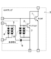
- FIG. 1 is a diagram showing a schematic configuration of an insulated gate semiconductor device 3 according to an embodiment of the present invention. The same parts as those of the conventional insulated gate semiconductor device 3 shown in FIG.
- the insulated gate semiconductor device 3 is characterized by an emitter electrode of a current detection insulated gate transistor (hereinafter referred to as a sense IGBT) 2 and an anode of a temperature detection diode 4 as shown in FIG.
- a sense IGBT current detection insulated gate transistor
- an electrostatic withstand Zener diode 6 is interposed between the electrodes.
- the anode electrode of the electrostatic withstand Zener diode 6 is connected to the emitter electrode of the insulated gate transistor 2 for current detection
- the cathode electrode of the electrostatic withstand Zener diode 6 is connected to the anode electrode of the temperature detecting diode 4.
- the electrostatic withstand Zener diode 6 is formed on the same semiconductor substrate together with the main insulated gate transistor (hereinafter referred to as main IGBT) 1, the sense IGBT 2, the temperature detection diode 4, and the like.
- main IGBT main insulated gate transistor
- the semiconductor substrate on which these elements are formed is realized as an insulated gate semiconductor device 3 that is modularized as a so-called IGBT chip.
- the main IGBT 1 and the sense IGBT 2 in the insulated gate semiconductor device (hereinafter referred to as IGBT chip) 3 form a collector region and an emitter region on the surface layer of the semiconductor substrate that is the base of the IGBT chip 3, and these collector regions
- an element structure in which a gate electrode is formed on an emitter region via an insulating layer is realized.
- the temperature detecting diode 4 is formed on the surface layer of the semiconductor substrate in the vicinity of the main IGBT 1 and the sense IGBT 2.
- the electrostatic withstand Zener diode 6 is formed so as to connect the emitter region of the sense IGBT 2 and the anode region of the temperature detecting diode 4 to the surface layer of the semiconductor substrate.
- the IGBT chip 3 configured as described above, even if static electricity is applied to the IGBT chip 3 from the outside and the surface potential of the semiconductor substrate increases, the voltage resulting from the electrostatic energy is absorbed by the temperature detection diode 4.
- the potential of the emitter electrode of the sense IGBT 2 connected to the anode electrode of the temperature detecting diode 4 via the electrostatic withstand Zener diode 6 can be kept low.
- the voltage applied between the emitter electrode and the gate electrode of the sense IGBT 2 can be kept low, and electrostatic breakdown of the sense IGBT 2 due to static electricity can be prevented.
- the IGBT chip 3 having such a configuration, it is only necessary to adopt a simple configuration in which the electrostatic withstand Zener diode 6 is interposed between the emitter electrode of the sense IGBT 2 and the anode electrode of the temperature detection diode 4. is there. Therefore, the IGBT chip 3 can be downsized as compared with the conventional case where a plurality of zener diodes for electrostatic discharge are provided between the gate electrode and the emitter electrode of the sense IGBT 2 in multiple stages. A great effect can be achieved in practical use.
- the electrostatic discharge zener diode 7 provided with the diode 8 in parallel is basically realized as an element structure similar to the temperature detection diode 4 provided with the zener diode (ZD) 5 in parallel. Therefore, there is almost no problem in integrally forming the electrostatic discharge Zener diode 7 having the diodes 8 in parallel with the IGBT chip 3, and the increase in the chip area of the IGBT chip 3 accompanying this is also slight. .
- the reverse withstand voltage of the electrostatic discharge Zener diode 7 interposed between the emitter electrode and the gate electrode of the sense IGBT 2 generally, about 30 V which is the drive voltage of the IGBT chip 3 is sufficient.
- the reverse breakdown voltage of the electrostatic discharge zener diode 7 may be set to, for example, 54 V or more as the test voltage. desirable.
- the reverse breakdown voltage of the Zener diode 7 for electrostatic discharge is, for example, the test.
- the voltage is desirably 54 V or higher.
Landscapes
- Semiconductor Integrated Circuits (AREA)
Abstract
【課題】主電流を制御するゲート電極を備えた主絶縁ゲート・トランジスタと、主絶縁ゲート・トランジスタに対して並列的に設けられて主絶縁ゲート・トランジスタに流れる主電流に比例した電流を出力する電流検出用絶縁ゲート・トランジスタと、これらの絶縁ゲート・トランジスタと共に同一の半導体基板上に形成された温度検出用ダイオードとを備えた絶縁ゲート半導体装置において静電気放電耐量の向上を図る。 【解決手段】電流検出用絶縁ゲート・トランジスタのエミッタ電極と、温度検出用ダイオードのアノード電極との間に静電気耐量用ツェナーダイオードを介装することで、温度検出用ダイオードを利用して電流検出用絶縁ゲート・トランジスタの静電気放電耐量を確保する。
Description
本発明は、静電気対策を施した簡易な構成の絶縁ゲート半導体装置に関する。
インバータ等の電力変換装置においては負荷ヘの供給電流を制御する半導体スイッチング素子として、例えば絶縁ゲート・トランジスタ(IGBTやMOS-FET)が用いられる。また電力変換装置においては、絶縁ゲート・トランジスタを介して負荷側に供給される電流を検出して、過電流から絶縁ゲート・トランジスタ等を保護する為の電流検出素子を組み込むことも多い。
ここで電流検出素子は、例えば図3に示すように主電流を制御するIGBTからなる主絶縁ゲート・トランジスタ(主IGBT)1に対して並列的に設けられて、主絶縁ゲート・トランジスタ1を介して流れる主電流に比例した電流を出力する電流検出用絶縁ゲート・トランジスタ(センスIGBT)2として実現される。具体的には電流検出用絶縁ゲート・トランジスタ2は、そのコレクタ電極およびゲート電極を主絶縁ゲート・トランジスタ1のコレクタ電極およびゲート電極にそれぞれ接続して設けられる。
ちなみに電流検出用絶縁ゲート・トランジスタ2は、専ら、主絶縁ゲート・トランジスタ1と共に、例えばSiやSiCからなる半導体基板(図示せず)内に集積して一体に形成され、絶縁ゲート半導体装置3として実現される。尚、電流検出用絶縁ゲート・トランジスタ2は、主絶縁ゲート・トランジスタ1に流れる主電流に比例した電流をエミッタ電極から出力する。そして絶縁ゲート半導体装置3には、主絶縁ゲート・トランジスタ1のコレクタ電極、エミッタ電極およびゲート電極、並びに電流検出用絶縁ゲート・トランジスタ2のエミッタ電極にそれぞれ接続された外部接続端子が設けられる。
またこの種の絶縁ゲート半導体装置(IGBTチップ)3には、主絶縁ゲート・トランジスタ1の動作温度を検出する為の温度検出用ダイオード4を組み込むことも多い。尚、温度検出用ダイオード4には、一般的には温度検出用ダイオード4に印加される電圧を規制して温度検出用ダイオード4のノイズによる誤動作を防ぐと共に、温度検出用ダイオード4の温度特性を補償する為のツェナーダイオード(ZD)5が並列接続される。このような構成の絶縁ゲート半導体装置3については、例えば特許文献1に詳しく紹介される(特許文献1の図2を参照)。
このような構成の絶縁ゲート半導体装置3は駆動回路11、電流検出回路12および温度検出回路13を備えた制御回路14により主絶縁ゲート・トランジスタ1がオン・オフ駆動されるように構成される。駆動回路11は、例えばP型のMOS-FETからなる出力トランジスタ15を介して主絶縁ゲート・トランジスタ1のゲート電極に駆動信号を印加して主絶縁ゲート・トランジスタ1をオン・オフ駆動する。
また電流検出回路12は、電流検出抵抗(Rs)16を介して電流検出用絶縁ゲート・トランジスタ2のエミッタ電極から出力される電流を電圧変換して検出することで、主絶縁ゲート・トランジスタ1に流れる主電流を監視する。そして電流検出回路12は、過大電流の検出時に駆動回路11の動作を停止させることで主絶縁ゲート・トランジスタ1をオフし、過大電流による主絶縁ゲート・トランジスタ1の過電流破壊を防止する。
更に温度検出回路13は、温度検出用ダイオード4を介して流れる電流から絶縁ゲート半導体装置3の動作温度、ひいては主絶縁ゲート・トランジスタ1の動作温度を検出する。そして制御回路14は、温度検出回路13により異常な温度上昇が検出されたときには駆動回路11の動作を停止させて主絶縁ゲート・トランジスタ1をオフし、これによって主絶縁ゲート・トランジスタ1を過熱破壊から防止する。
ところで上述した絶縁ゲート半導体装置3においては、人体モードとマシンモードの静電気放電耐量ESD (ElectroStatic-Discharge)による、絶縁ゲート半導体装置内のゲート酸化膜や層間絶縁膜の絶縁破壊が問題となる。電流検出用絶縁ゲート・トランジスタ2は、例えば主絶縁ゲート・トランジスタ1に流れる主電流に比例した1/数百~1/10000程度の電流を流す素子として設計するため、電流検出用絶縁ゲート・トランジスタ2の面積は1/数百~1/10000程度であり、絶縁ゲート・トランジスタ内のゲート酸化膜や層間絶縁膜により形成される寄生容量値に比例する。この為、電流検出用絶縁ゲート・トランジスタ2のESD耐量が主絶縁ゲート・トランジスタ1に比べて非常に小さくなる。
これに対して電流検出用絶縁ゲート・トランジスタ2の出力特性を変えずに静電気放電耐量を高める手段として、例えば特許文献2にあるような静電気放電用のダイオードを介装し、ダイオードの静耐圧とPNジャンクションの接合面積の大きさで保護する技術が公知である。(特許文献2の図1を参照)。
しかしながら、センスIGBTからなる電流検出用絶縁ゲート・トランジスタ2のエミッタ電極とゲート電極との間に静電気放電用のダイオードを介装する場合、所望とする静電気放電耐量を確保するには静電気放電用のダイオードとして、静耐圧とPNジャンクションの接合面積の大きさを確保する必要があり、例えば所定の降伏電圧特性を有するツェナーダイオードを複数段に亘って直列に接続して設けることが必要である。複数のツェナーダイオードからなる静電気放電用のダイオードを設ける場合、IGBTチップからなる絶縁ゲート半導体装置3における静電気放電用のダイオード(複数のツェナーダイオード)の占有面積が大きくなり、IGBTチップ(絶縁ゲート半導体装置)3 面積を大きくする必要が生じる。
本発明はこのような事情を考慮してなされたもので、その目的は、主絶縁ゲート・トランジスタと、この主絶縁ゲート・トランジスタに流れる主電流に比例した電流を出力する電流検出用絶縁ゲート・トランジスタとを備えた絶縁ゲート半導体装置において、特に電流検出用絶縁ゲート・トランジスタに対する静電気放電耐量を高めた簡易な構成の絶縁ゲート半導体装置を提供することにある。
本発明は、主絶縁ゲート・トランジスタと、この主絶縁ゲート・トランジスタに対して並列的に設けられた電流検出用絶縁ゲート・トランジスタとを備えて構成される絶縁ゲート半導体装置が、一般的には更に温度検出用ダイオードを備えることに着目してなされている。
即ち、本発明に係る絶縁ゲート半導体装置は、基本的にはコレクタ電極とエミッタ電極との間に流れる主電流を制御するゲート電極を備えた主絶縁ゲート・トランジスタ(主IGBT)と、コレクタ電極およびゲート電極を前記主絶縁ゲート・トランジスタ(主IGBT)のコレクタ電極とゲート電極にそれぞれ接続して設けられて前記主絶縁ゲート・トランジスタ(主IGBT)に流れる主電流に比例した電流をエミッタ電極から出力する電流検出用絶縁ゲート・トランジスタ(センスIGBT)とを備える。更に絶縁ゲート半導体装置は、アノード電極とカソード電極とを備え、前記主絶縁ゲート・トランジスタおよび前記電流検出用絶縁ゲート・トランジスタと共に同一の基板上に形成された温度検出用ダイオードとを備えて構成される。
特に本発明に係る絶縁ゲート半導体装置は、上述した目的を達成するべく前記電流検出用絶縁ゲート・トランジスタのエミッタ電極にアノード電極を接続し、カソード電極を前記温度検出用ダイオードのアノード電極に接続した静電気耐量用ツェナーダイオードを前記基板上に形成したことを特徴としている。
ちなみに前記主絶縁ゲート・トランジスタのコレクタ電極、エミッタ電極およびゲート電極と、前記電流検出用絶縁ゲート・トランジスタのエミッタ電極、並びに前記温度検出用ダイオードのアノード電極およびカソード電極は、絶縁ゲート半導体装置における互いに独立した複数の接続端子にそれぞれ個別に接続して設けられる。
好ましくは前記温度検出用ダイオードは、例えば該温度検出用ダイオードに加わる電圧を規定する過電圧保護用ツェナーダイオードを並列接続して前記基板上に形成される。
また本発明に係る絶縁ゲート半導体装置は、更に前記電流検出用絶縁ゲート・トランジスタのエミッタ電極にアノード電極を接続すると共に、カソード電極を前記電流検出用絶縁ゲート・トランジスタのゲート電極に接続した静電気放電用ツェナーダイオードを備えて構成される。
このように構成された絶縁ゲート半導体装置によれば、電流検出用絶縁ゲート・トランジスタのエミッタ電極と前記温度検出用ダイオードのアノード電極との間に静電気放電耐量用のツェナーダイオードを介装するという簡易な構成で、前記温度検出用ダイオードを前記電流検出用絶縁ゲート・トランジスタの静電気放電耐量の確保に利用することが可能となる。即ち、上記構成によれば前記電流検出用絶縁ゲート・トランジスタの静電気放電耐量は、前記温度検出用ダイオードの静電気放電耐量との相乗効果が得られる。この結果、従来の電流検出用絶縁ゲート・トランジスタの静電気放電耐量 < 温度検出用ダイオードの静電耐量の関係から、温度検出用ダイオードの静電耐量 < 電流検出用絶縁ゲート・トランジスタの静電気放電耐量=温度検出用ダイオードの静電耐量の関係の向上効果が得られ、電流検出用絶縁ゲート・トランジスタの静電気放電耐量に関しては従来の3倍、温度検出用ダイオードの静電耐量に関しては従来の1.5倍に向上する。
従って前記主絶縁ゲート・トランジスタと前記電流検出用絶縁ゲート・トランジスタとに加えて前記温度検出用ダイオードとを備えた絶縁ゲート半導体装置において、更に上述した如く前記静電気放電耐量用ダイオードを設けると言う簡易な構成でありながら、前記電流検出用絶縁ゲート・トランジスタに対する静電気放電耐量を十分に確保することが可能となる。更には、例えば1つの静電気放電耐量用ツェナーダイオードを追加するだけなので、電流検出用絶縁ゲート・トランジスタのゲート電極とエミッタ電極との間に静電気放電用の複数のツェナーダイオードを多段に設ける場合に比較して、絶縁ゲート半導体装置の小型化を図ることが可能となる等の実用上多大なる効果が奏せられる。
以下、図面を参照して本発明の一実施形態に係る絶縁ゲート半導体装置について説明する。
図1は本発明の一実施形態に係る絶縁ゲート半導体装置3の概略構成を示す図である。尚、図3に示した従来の絶縁ゲート半導体装置3と同一部分には同一符号を付し、その説明を省略する。
この実施形態に係る絶縁ゲート半導体装置3が特徴とするところは、図3に示すように電流検出用絶縁ゲート・トランジスタ(以下、センスIGBTと称す)2のエミッタ電極と温度検出用ダイオード4のアノード電極との間に静電気耐量用ツェナーダイオード6を介装した点にある。具体的には静電気耐量用ツェナーダイオード6のアノード電極を電流検出用絶縁ゲート・トランジスタ2のエミッタ電極に接続し、該静電気耐量用ツェナーダイオード6のカソード電極を温度検出用ダイオード4のアノード電極に接続して設ける。
ちなみに静電気耐量用ツェナーダイオード6は、主絶縁ゲート・トランジスタ(以下、主IGBTと称す)1、センスIGBT2および温度検出用ダイオード4等と共に同一の半導体基板上に形成される。そしてこれらの素子を形成した半導体基板は、いわゆるIGBTチップとしてモジュール化された絶縁ゲート半導体装置3として実現される。
ここで絶縁ゲート半導体装置(以下、IGBTチップと称す)3における主IGBT1およびセンスIGBT2は、IGBTチップ3の基体である半導体基板の表面層にコレクタ領域とエミッタ領域とを形成し、これらのコレクタ領域およびエミッタ領域上に絶縁層を介してゲート電極を形成した素子構造として実現される。また温度検出用ダイオード4は、主IGBT1およびセンスIGBT2の近傍の半導体基板の表面層に形成される。そして静電気耐量用ツェナーダイオード6は、半導体基板の表面層にセンスIGBT2のエミッタ領域と、温度検出用ダイオード4のアノード領域とを接続するように形成される。
このように構成されたIGBTチップ3によれば、IGBTチップ3に外部から静電気が加わり、半導体基板の表面電位が高くなっても、その静電気エネルギに起因する電圧は温度検出用ダイオード4により吸収される。すると温度検出用ダイオード4のアノード電極に静電気耐量用ツェナーダイオード6を介して接続されたセンスIGBT2のエミッタ電極の電位も低く抑えられる。この結果、センスIGBT2のエミッタ電極とゲート電極との間に加わる電圧を低く抑えることが可能となり、静電気によるセンスIGBT2の静電破壊を防ぐことが可能となる。
即ち、IGBTチップ3に加わる高電圧の静電気を、静電気耐量用ツェナーダイオード6を介して温度検出用ダイオード4により受け止めることができる。この結果、静電気に起因してセンスIGBT2のゲート電極とエミッタ電極との間に加わる電圧を低く抑えることが可能となる。故に、温度検出用ダイオード4の静電耐量を有効に利用してセンスIGBT2の静電破壊を効果的に防止することが可能となる。
またこのような構成のIGBTチップ3によれば、センスIGBT2のエミッタ電極と、温度検出用ダイオード4のアノード電極との間に静電気耐量用ツェナーダイオード6を介装した簡易な構成を採用するだけである。従って従来のようにセンスIGBT2のゲート電極とエミッタ電極との間に静電気放電用の複数のツェナーダイオードを多段に設ける場合に比較して、IGBTチップ3の小型化を図ることが可能となる等の実用上多大なる効果が奏せられる。
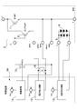
尚、本発明は上述した実施形態に限定されるものではない。例えば図2に示すように静電気耐量用ツェナーダイオード6に加えて、センスIGBT2のエミッタ電極とゲート電極との間に静電気放電用ツェナーダイオード7を設けることも可能である。この場合、センスIGBT2の通常動作を保証する上で、静電気放電用ツェナーダイオード7と逆並列にダイオード8を設けてセンスIGBT2のゲート電極に印加されるゲート電圧が静電気により不本意に高くなることを防止することが好ましい。
またこのようなダイオード8を並列に備えた静電気放電用ツェナーダイオード7については、基本的にはツェナーダイオード(ZD)5を並列に備えた温度検出用ダイオード4と同様な素子構造として実現される。従ってダイオード8を並列に備えた静電気放電用ツェナーダイオード7をIGBTチップ3に一体に集積形成する上で殆ど問題となることはなく、またこれに伴うIGBTチップ3のチップ面積の増大も僅かである。
尚、センスIGBT2のエミッタ電極とゲート電極との間に介装される静電気放電用ツェナーダイオード7の逆耐圧については、一般的にはIGBTチップ3の駆動電圧である30V程度であれば十分である。しかし主IGBT1およびセンスIGBT2のゲート酸化膜に対する初期クリーニング試験、即ち、ゲートショック試験を考慮した場合には、静電気放電用ツェナーダイオード7の逆耐圧を、例えばその試験電圧である54V以上にすることが望ましい。またゲート酸化膜の信頼性試験である、いわゆるTZDB(Time Zero Dielectric Breakdown)試験やTDDB(Time Dependent Dielectric Breakdown)試験を考慮した場合には、静電気放電用ツェナーダイオード7の逆耐圧を、例えばその試験電圧である54V以上にすることが望ましい。
しかし温度検出用ダイオード4を利用してセンスIGBT2の静電気耐量を確保しているので、上述した程、静電気放電用ツェナーダイオード7の逆耐圧を高めなくても十分である。その他、本発明はその要旨を逸脱しない範囲で種々変形して実施することができる。
1 主絶縁ゲート・トランジスタ(主IGBT)
2 電流検出用絶縁ゲート・トランジスタ(センスIGBT)
3 絶縁ゲート半導体装置(IGBTチップ)
4 温度検出用ダイオード
5 ツェナーダイオード(ZD)
6 静電気耐量用ツェナーダイオード
7 静電気放電用ツェナーダイオード
11 駆動回路
12 電流検出回路
13 温度検出回路
14 制御回路
15 出力トランジスタ(MOS-FET)
16 電流検出抵抗(Rs)
2 電流検出用絶縁ゲート・トランジスタ(センスIGBT)
3 絶縁ゲート半導体装置(IGBTチップ)
4 温度検出用ダイオード
5 ツェナーダイオード(ZD)
6 静電気耐量用ツェナーダイオード
7 静電気放電用ツェナーダイオード
11 駆動回路
12 電流検出回路
13 温度検出回路
14 制御回路
15 出力トランジスタ(MOS-FET)
16 電流検出抵抗(Rs)
Claims (4)
- コレクタ電極とエミッタ電極との間に流れる主電流を制御するゲート電極を備えた主絶縁ゲート・トランジスタと、
コレクタ電極およびゲート電極を前記主絶縁ゲート・トランジスタのコレクタ電極とゲート電極にそれぞれ接続して設けられて前記主絶縁ゲート・トランジスタに流れる主電流に比例した電流をエミッタ電極から出力する電流検出用絶縁ゲート・トランジスタと、
アノード電極とカソード電極とを備え、前記主絶縁ゲート・トランジスタおよび前記電流検出用絶縁ゲート・トランジスタと共に一つの半導体基板上に形成された温度検出用ダイオードと、
前記電流検出用絶縁ゲート・トランジスタのエミッタ電極にアノード電極を接続し、カソード電極を前記温度検出用ダイオードのアノード電極に接続して前記半導体基板上に形成された静電気耐量用ツェナーダイオードと
を具備したことを特徴とする絶縁ゲート半導体装置。 - 前記主絶縁ゲート・トランジスタのコレクタ電極、エミッタ電極およびゲート電極、前記電流検出用絶縁ゲート・トランジスタのエミッタ電極、並びに前記温度検出用ダイオードのアノード電極およびカソード電極は、互いに独立した複数の接続端子にそれぞれ個別に接続されている請求項1に記載の絶縁ゲート半導体装置。
- 前記温度検出用ダイオードは、該温度検出用ダイオードに加わる電圧を規定する過電圧保護用ツェナーダイオードを並列接続して前記半導体基板上に形成されるものである請求項1に記載の絶縁ゲート半導体装置。
- 請求項1に記載の絶縁ゲート半導体装置において、
更に前記電流検出用絶縁ゲート・トランジスタのエミッタ電極にアノード電極を接続すると共に、カソード電極を前記電流検出用絶縁ゲート・トランジスタのゲート電極に接続した静電気放電用ツェナーダイオードを前記半導体基板上に備えることを特徴とする絶縁ゲート半導体装置。
Priority Applications (3)
| Application Number | Priority Date | Filing Date | Title |
|---|---|---|---|
| CN201780002760.8A CN107924872B (zh) | 2016-02-18 | 2017-01-04 | 绝缘栅半导体装置 |
| JP2017567979A JP6406464B2 (ja) | 2016-02-18 | 2017-01-04 | 絶縁ゲート半導体装置 |
| US15/890,723 US10290625B2 (en) | 2016-02-18 | 2018-02-07 | Insulated gate semiconductor device |
Applications Claiming Priority (2)
| Application Number | Priority Date | Filing Date | Title |
|---|---|---|---|
| JP2016029355 | 2016-02-18 | ||
| JP2016-029355 | 2016-02-18 |
Related Child Applications (1)
| Application Number | Title | Priority Date | Filing Date |
|---|---|---|---|
| US15/890,723 Continuation US10290625B2 (en) | 2016-02-18 | 2018-02-07 | Insulated gate semiconductor device |
Publications (1)
| Publication Number | Publication Date |
|---|---|
| WO2017141560A1 true WO2017141560A1 (ja) | 2017-08-24 |
Family
ID=59625764
Family Applications (1)
| Application Number | Title | Priority Date | Filing Date |
|---|---|---|---|
| PCT/JP2017/000053 Ceased WO2017141560A1 (ja) | 2016-02-18 | 2017-01-04 | 絶縁ゲート半導体装置 |
Country Status (4)
| Country | Link |
|---|---|
| US (1) | US10290625B2 (ja) |
| JP (1) | JP6406464B2 (ja) |
| CN (1) | CN107924872B (ja) |
| WO (1) | WO2017141560A1 (ja) |
Cited By (4)
| Publication number | Priority date | Publication date | Assignee | Title |
|---|---|---|---|---|
| JP2019086306A (ja) * | 2017-11-01 | 2019-06-06 | トヨタ自動車株式会社 | 半導体装置の試験装置 |
| WO2020255617A1 (ja) * | 2019-06-21 | 2020-12-24 | ローム株式会社 | 半導体装置およびその製造方法 |
| WO2021059881A1 (ja) * | 2019-09-25 | 2021-04-01 | 富士電機株式会社 | 半導体装置 |
| US11830871B2 (en) | 2020-02-21 | 2023-11-28 | Fuji Electric Co., Ltd. | Semiconductor device and method for fabricating semiconductor device |
Families Citing this family (6)
| Publication number | Priority date | Publication date | Assignee | Title |
|---|---|---|---|---|
| US10802053B2 (en) * | 2016-09-22 | 2020-10-13 | Infineon Technologies Ag | Configuration of integrated current flow sensor |
| TWI743384B (zh) * | 2018-07-31 | 2021-10-21 | 立積電子股份有限公司 | 反並聯二極體裝置 |
| EP3608644B1 (de) * | 2018-08-09 | 2021-03-24 | Infineon Technologies AG | Verfahren zum bestimmen eines vorzeichens eines laststroms in einer brückenschaltung mit mindestenes einer leistungshalbleiterschaltung |
| KR102539366B1 (ko) * | 2019-10-09 | 2023-06-01 | 세미컨덕터 콤포넨츠 인더스트리즈 엘엘씨 | 제너 다이오드를 사용하는 감지 igbt에 대한 정전기 방전 처리 |
| US11201144B2 (en) | 2019-10-09 | 2021-12-14 | Semiconductor Components Industries, Llc | Electrostatic discharge handling for sense IGBT using Zener diode |
| US11942471B2 (en) | 2020-11-13 | 2024-03-26 | Renesas Electronics Corporation | Semiconductor chip, semiconductor device and manufacturing method of semiconductor device |
Citations (5)
| Publication number | Priority date | Publication date | Assignee | Title |
|---|---|---|---|---|
| JP2004515911A (ja) * | 2000-09-29 | 2004-05-27 | 松下電工株式会社 | 保護機能付き半導体装置 |
| JP2007266089A (ja) * | 2006-03-27 | 2007-10-11 | Toyota Motor Corp | 半導体装置 |
| JP2007287919A (ja) * | 2006-04-17 | 2007-11-01 | Toyota Industries Corp | 温度検出機能付き半導体装置 |
| JP2008042950A (ja) * | 2006-08-01 | 2008-02-21 | Mitsubishi Electric Corp | 電力変換装置 |
| JP2008153615A (ja) * | 2006-11-21 | 2008-07-03 | Denso Corp | 電力用半導体装置 |
Family Cites Families (17)
| Publication number | Priority date | Publication date | Assignee | Title |
|---|---|---|---|---|
| DE3723786A1 (de) * | 1987-07-16 | 1989-01-26 | Licentia Gmbh | Anordnung zur selbsttaetigen ueberstromabschaltung |
| JPH04322126A (ja) | 1991-04-22 | 1992-11-12 | Hitachi Ltd | 電流制限回路 |
| JP3139223B2 (ja) | 1992-11-26 | 2001-02-26 | 富士電機株式会社 | 半導体装置及びその製造方法 |
| JP3243902B2 (ja) | 1993-09-17 | 2002-01-07 | 株式会社日立製作所 | 半導体装置 |
| JP2004111438A (ja) * | 2002-09-13 | 2004-04-08 | Toshiba Corp | Mosゲート素子の過電圧保護回路 |
| CN101317321A (zh) * | 2005-11-29 | 2008-12-03 | 丰田自动车株式会社 | 用于电动车辆的dc-dc变压器 |
| JP4706462B2 (ja) | 2005-12-07 | 2011-06-22 | トヨタ自動車株式会社 | 電流検出機能を有する半導体装置 |
| JP4816182B2 (ja) * | 2006-03-23 | 2011-11-16 | 株式会社日立製作所 | スイッチング素子の駆動回路 |
| JP4973057B2 (ja) | 2006-08-07 | 2012-07-11 | トヨタ自動車株式会社 | 半導体装置 |
| US7573687B2 (en) | 2006-11-21 | 2009-08-11 | Denso Corporation | Power semiconductor device |
| CN101325363B (zh) * | 2008-06-26 | 2011-11-16 | 申莉萌 | 自带动态电源的谐振驱动模块控制方法 |
| JP5340018B2 (ja) | 2009-05-01 | 2013-11-13 | 三菱電機株式会社 | 半導体装置 |
| WO2013005520A1 (ja) | 2011-07-06 | 2013-01-10 | 富士電機株式会社 | パワー半導体デバイスの電流補正回路および電流補正方法 |
| CN202798435U (zh) * | 2012-08-22 | 2013-03-13 | 成都中大华瑞科技有限公司 | 高性能低成本igbt负压自举驱动电路 |
| CN203788256U (zh) * | 2013-12-26 | 2014-08-20 | 国家电网公司 | 一种断路器仿真仪上使用的开出控制装置 |
| CN107949986B (zh) * | 2016-03-04 | 2021-05-18 | 富士电机株式会社 | 半导体元件的驱动装置 |
| JP2018059448A (ja) * | 2016-10-05 | 2018-04-12 | 富士電機株式会社 | 内燃機関用点火装置 |
-
2017
- 2017-01-04 JP JP2017567979A patent/JP6406464B2/ja active Active
- 2017-01-04 WO PCT/JP2017/000053 patent/WO2017141560A1/ja not_active Ceased
- 2017-01-04 CN CN201780002760.8A patent/CN107924872B/zh active Active
-
2018
- 2018-02-07 US US15/890,723 patent/US10290625B2/en active Active
Patent Citations (5)
| Publication number | Priority date | Publication date | Assignee | Title |
|---|---|---|---|---|
| JP2004515911A (ja) * | 2000-09-29 | 2004-05-27 | 松下電工株式会社 | 保護機能付き半導体装置 |
| JP2007266089A (ja) * | 2006-03-27 | 2007-10-11 | Toyota Motor Corp | 半導体装置 |
| JP2007287919A (ja) * | 2006-04-17 | 2007-11-01 | Toyota Industries Corp | 温度検出機能付き半導体装置 |
| JP2008042950A (ja) * | 2006-08-01 | 2008-02-21 | Mitsubishi Electric Corp | 電力変換装置 |
| JP2008153615A (ja) * | 2006-11-21 | 2008-07-03 | Denso Corp | 電力用半導体装置 |
Cited By (15)
| Publication number | Priority date | Publication date | Assignee | Title |
|---|---|---|---|---|
| JP2019086306A (ja) * | 2017-11-01 | 2019-06-06 | トヨタ自動車株式会社 | 半導体装置の試験装置 |
| WO2020255617A1 (ja) * | 2019-06-21 | 2020-12-24 | ローム株式会社 | 半導体装置およびその製造方法 |
| JPWO2020255617A1 (ja) * | 2019-06-21 | 2020-12-24 | ||
| US12062655B2 (en) | 2019-06-21 | 2024-08-13 | Rohm Co., Ltd. | Semiconductor device and method for manufacturing same |
| JP7116847B2 (ja) | 2019-06-21 | 2022-08-10 | ローム株式会社 | 半導体装置およびその製造方法 |
| WO2021060545A1 (ja) * | 2019-09-25 | 2021-04-01 | 富士電機株式会社 | 半導体装置およびシステム |
| JPWO2021059881A1 (ja) * | 2019-09-25 | 2021-04-01 | ||
| JPWO2021060545A1 (ja) * | 2019-09-25 | 2021-04-01 | ||
| JP7243845B2 (ja) | 2019-09-25 | 2023-03-22 | 富士電機株式会社 | 半導体装置 |
| JP7243844B2 (ja) | 2019-09-25 | 2023-03-22 | 富士電機株式会社 | 半導体装置およびシステム |
| WO2021059881A1 (ja) * | 2019-09-25 | 2021-04-01 | 富士電機株式会社 | 半導体装置 |
| US12094960B2 (en) | 2019-09-25 | 2024-09-17 | Fuji Electric Co., Ltd. | Semiconductor device and system |
| US12159928B2 (en) | 2019-09-25 | 2024-12-03 | Fuji Electric Co., Ltd. | Semiconductor device |
| US11830871B2 (en) | 2020-02-21 | 2023-11-28 | Fuji Electric Co., Ltd. | Semiconductor device and method for fabricating semiconductor device |
| US12426352B2 (en) | 2020-02-21 | 2025-09-23 | Fuji Electric Co., Ltd. | Semiconductor device and method for fabricating semiconductor device |
Also Published As
| Publication number | Publication date |
|---|---|
| CN107924872B (zh) | 2022-03-04 |
| JP6406464B2 (ja) | 2018-10-17 |
| US20180166436A1 (en) | 2018-06-14 |
| CN107924872A (zh) | 2018-04-17 |
| JPWO2017141560A1 (ja) | 2018-06-21 |
| US10290625B2 (en) | 2019-05-14 |
Similar Documents
| Publication | Publication Date | Title |
|---|---|---|
| JP6406464B2 (ja) | 絶縁ゲート半導体装置 | |
| JP4993092B2 (ja) | レベルシフト回路および半導体装置 | |
| JP5157247B2 (ja) | 電力半導体装置 | |
| TWI622240B (zh) | 固態故障電流限制裝置、用於限制故障電流的方法和系統 | |
| CN103527381B (zh) | 单片式点火器和内燃机点火装置 | |
| US20120243133A1 (en) | Electrostatic discharge protection circuit | |
| US8164871B2 (en) | Circuit for protecting an integrated circuit against elctrostatic discharges in CMOS technology | |
| JP5340018B2 (ja) | 半導体装置 | |
| CN105577153A (zh) | 半导体装置 | |
| CN104051453A (zh) | 有源esd保护电路 | |
| CN103701442A (zh) | 用于高频切换的功率半导体器件的有源钳位保护电路 | |
| CN105940607A (zh) | 半导体装置 | |
| US8017996B2 (en) | Semiconductor device, and energy transmission device using the same | |
| JP2006166691A (ja) | 電力用半導体装置 | |
| US8570780B2 (en) | Semiconductor device | |
| JP6299254B2 (ja) | 半導体装置、スイッチング電源用制御icおよびスイッチング電源装置 | |
| JP7002431B2 (ja) | 半導体装置 | |
| JP2014013798A (ja) | ワンチップイグナイタ及び内燃機関点火装置 | |
| JP2014013796A (ja) | ワンチップイグナイタ及び内燃機関点火装置 | |
| US10236874B2 (en) | Overvoltage protection circuit for a power semiconductor and method for protecting a power semiconductor from over-voltages | |
| EP2618487A2 (en) | Switching circuit and power supply device | |
| KR101904682B1 (ko) | 전류 차단 장치 | |
| KR20190101418A (ko) | 전기 장비를 보호하기 위한 장치 | |
| KR20100080186A (ko) | 전력 변환 회로 | |
| JP2014013797A (ja) | ワンチップイグナイタ及び内燃機関点火装置 |
Legal Events
| Date | Code | Title | Description |
|---|---|---|---|
| 121 | Ep: the epo has been informed by wipo that ep was designated in this application |
Ref document number: 17752824 Country of ref document: EP Kind code of ref document: A1 |
|
| ENP | Entry into the national phase |
Ref document number: 2017567979 Country of ref document: JP Kind code of ref document: A |
|
| NENP | Non-entry into the national phase |
Ref country code: DE |
|
| 122 | Ep: pct application non-entry in european phase |
Ref document number: 17752824 Country of ref document: EP Kind code of ref document: A1 |