WO2017111082A1 - Procédé de production de fibre optique et dispositif d'irradiation de lumière ultraviolette - Google Patents
Procédé de production de fibre optique et dispositif d'irradiation de lumière ultraviolette Download PDFInfo
- Publication number
- WO2017111082A1 WO2017111082A1 PCT/JP2016/088486 JP2016088486W WO2017111082A1 WO 2017111082 A1 WO2017111082 A1 WO 2017111082A1 JP 2016088486 W JP2016088486 W JP 2016088486W WO 2017111082 A1 WO2017111082 A1 WO 2017111082A1
- Authority
- WO
- WIPO (PCT)
- Prior art keywords
- ultraviolet
- optical fiber
- ultraviolet irradiation
- light emitting
- semiconductor
- Prior art date
Links
Images


Classifications
-
- F—MECHANICAL ENGINEERING; LIGHTING; HEATING; WEAPONS; BLASTING
- F21—LIGHTING
- F21V—FUNCTIONAL FEATURES OR DETAILS OF LIGHTING DEVICES OR SYSTEMS THEREOF; STRUCTURAL COMBINATIONS OF LIGHTING DEVICES WITH OTHER ARTICLES, NOT OTHERWISE PROVIDED FOR
- F21V15/00—Protecting lighting devices from damage
- F21V15/01—Housings, e.g. material or assembling of housing parts
-
- C—CHEMISTRY; METALLURGY
- C03—GLASS; MINERAL OR SLAG WOOL
- C03C—CHEMICAL COMPOSITION OF GLASSES, GLAZES OR VITREOUS ENAMELS; SURFACE TREATMENT OF GLASS; SURFACE TREATMENT OF FIBRES OR FILAMENTS MADE FROM GLASS, MINERALS OR SLAGS; JOINING GLASS TO GLASS OR OTHER MATERIALS
- C03C25/00—Surface treatment of fibres or filaments made from glass, minerals or slags
- C03C25/10—Coating
- C03C25/24—Coatings containing organic materials
- C03C25/26—Macromolecular compounds or prepolymers
-
- B—PERFORMING OPERATIONS; TRANSPORTING
- B05—SPRAYING OR ATOMISING IN GENERAL; APPLYING FLUENT MATERIALS TO SURFACES, IN GENERAL
- B05C—APPARATUS FOR APPLYING FLUENT MATERIALS TO SURFACES, IN GENERAL
- B05C9/00—Apparatus or plant for applying liquid or other fluent material to surfaces by means not covered by any preceding group, or in which the means of applying the liquid or other fluent material is not important
- B05C9/08—Apparatus or plant for applying liquid or other fluent material to surfaces by means not covered by any preceding group, or in which the means of applying the liquid or other fluent material is not important for applying liquid or other fluent material and performing an auxiliary operation
- B05C9/14—Apparatus or plant for applying liquid or other fluent material to surfaces by means not covered by any preceding group, or in which the means of applying the liquid or other fluent material is not important for applying liquid or other fluent material and performing an auxiliary operation the auxiliary operation involving heating or cooling
-
- B—PERFORMING OPERATIONS; TRANSPORTING
- B29—WORKING OF PLASTICS; WORKING OF SUBSTANCES IN A PLASTIC STATE IN GENERAL
- B29C—SHAPING OR JOINING OF PLASTICS; SHAPING OF MATERIAL IN A PLASTIC STATE, NOT OTHERWISE PROVIDED FOR; AFTER-TREATMENT OF THE SHAPED PRODUCTS, e.g. REPAIRING
- B29C33/00—Moulds or cores; Details thereof or accessories therefor
- B29C33/02—Moulds or cores; Details thereof or accessories therefor with incorporated heating or cooling means
- B29C33/06—Moulds or cores; Details thereof or accessories therefor with incorporated heating or cooling means using radiation, e.g. electro-magnetic waves, induction heating
-
- B—PERFORMING OPERATIONS; TRANSPORTING
- B29—WORKING OF PLASTICS; WORKING OF SUBSTANCES IN A PLASTIC STATE IN GENERAL
- B29C—SHAPING OR JOINING OF PLASTICS; SHAPING OF MATERIAL IN A PLASTIC STATE, NOT OTHERWISE PROVIDED FOR; AFTER-TREATMENT OF THE SHAPED PRODUCTS, e.g. REPAIRING
- B29C35/00—Heating, cooling or curing, e.g. crosslinking or vulcanising; Apparatus therefor
- B29C35/02—Heating or curing, e.g. crosslinking or vulcanizing during moulding, e.g. in a mould
- B29C35/08—Heating or curing, e.g. crosslinking or vulcanizing during moulding, e.g. in a mould by wave energy or particle radiation
- B29C35/0888—Heating or curing, e.g. crosslinking or vulcanizing during moulding, e.g. in a mould by wave energy or particle radiation using transparant moulds
-
- B—PERFORMING OPERATIONS; TRANSPORTING
- B29—WORKING OF PLASTICS; WORKING OF SUBSTANCES IN A PLASTIC STATE IN GENERAL
- B29C—SHAPING OR JOINING OF PLASTICS; SHAPING OF MATERIAL IN A PLASTIC STATE, NOT OTHERWISE PROVIDED FOR; AFTER-TREATMENT OF THE SHAPED PRODUCTS, e.g. REPAIRING
- B29C35/00—Heating, cooling or curing, e.g. crosslinking or vulcanising; Apparatus therefor
- B29C35/02—Heating or curing, e.g. crosslinking or vulcanizing during moulding, e.g. in a mould
- B29C35/08—Heating or curing, e.g. crosslinking or vulcanizing during moulding, e.g. in a mould by wave energy or particle radiation
- B29C35/10—Heating or curing, e.g. crosslinking or vulcanizing during moulding, e.g. in a mould by wave energy or particle radiation for articles of indefinite length
-
- C—CHEMISTRY; METALLURGY
- C03—GLASS; MINERAL OR SLAG WOOL
- C03C—CHEMICAL COMPOSITION OF GLASSES, GLAZES OR VITREOUS ENAMELS; SURFACE TREATMENT OF GLASS; SURFACE TREATMENT OF FIBRES OR FILAMENTS MADE FROM GLASS, MINERALS OR SLAGS; JOINING GLASS TO GLASS OR OTHER MATERIALS
- C03C25/00—Surface treatment of fibres or filaments made from glass, minerals or slags
- C03C25/10—Coating
- C03C25/104—Coating to obtain optical fibres
- C03C25/106—Single coatings
-
- C—CHEMISTRY; METALLURGY
- C03—GLASS; MINERAL OR SLAG WOOL
- C03C—CHEMICAL COMPOSITION OF GLASSES, GLAZES OR VITREOUS ENAMELS; SURFACE TREATMENT OF GLASS; SURFACE TREATMENT OF FIBRES OR FILAMENTS MADE FROM GLASS, MINERALS OR SLAGS; JOINING GLASS TO GLASS OR OTHER MATERIALS
- C03C25/00—Surface treatment of fibres or filaments made from glass, minerals or slags
- C03C25/10—Coating
- C03C25/12—General methods of coating; Devices therefor
-
- C—CHEMISTRY; METALLURGY
- C03—GLASS; MINERAL OR SLAG WOOL
- C03C—CHEMICAL COMPOSITION OF GLASSES, GLAZES OR VITREOUS ENAMELS; SURFACE TREATMENT OF GLASS; SURFACE TREATMENT OF FIBRES OR FILAMENTS MADE FROM GLASS, MINERALS OR SLAGS; JOINING GLASS TO GLASS OR OTHER MATERIALS
- C03C25/00—Surface treatment of fibres or filaments made from glass, minerals or slags
- C03C25/62—Surface treatment of fibres or filaments made from glass, minerals or slags by application of electric or wave energy; by particle radiation or ion implantation
- C03C25/6206—Electromagnetic waves
- C03C25/6226—Ultraviolet
-
- C—CHEMISTRY; METALLURGY
- C23—COATING METALLIC MATERIAL; COATING MATERIAL WITH METALLIC MATERIAL; CHEMICAL SURFACE TREATMENT; DIFFUSION TREATMENT OF METALLIC MATERIAL; COATING BY VACUUM EVAPORATION, BY SPUTTERING, BY ION IMPLANTATION OR BY CHEMICAL VAPOUR DEPOSITION, IN GENERAL; INHIBITING CORROSION OF METALLIC MATERIAL OR INCRUSTATION IN GENERAL
- C23C—COATING METALLIC MATERIAL; COATING MATERIAL WITH METALLIC MATERIAL; SURFACE TREATMENT OF METALLIC MATERIAL BY DIFFUSION INTO THE SURFACE, BY CHEMICAL CONVERSION OR SUBSTITUTION; COATING BY VACUUM EVAPORATION, BY SPUTTERING, BY ION IMPLANTATION OR BY CHEMICAL VAPOUR DEPOSITION, IN GENERAL
- C23C16/00—Chemical coating by decomposition of gaseous compounds, without leaving reaction products of surface material in the coating, i.e. chemical vapour deposition [CVD] processes
- C23C16/44—Chemical coating by decomposition of gaseous compounds, without leaving reaction products of surface material in the coating, i.e. chemical vapour deposition [CVD] processes characterised by the method of coating
- C23C16/54—Apparatus specially adapted for continuous coating
- C23C16/545—Apparatus specially adapted for continuous coating for coating elongated substrates
-
- G—PHYSICS
- G02—OPTICS
- G02B—OPTICAL ELEMENTS, SYSTEMS OR APPARATUS
- G02B6/00—Light guides; Structural details of arrangements comprising light guides and other optical elements, e.g. couplings
- G02B6/44—Mechanical structures for providing tensile strength and external protection for fibres, e.g. optical transmission cables
-
- H—ELECTRICITY
- H05—ELECTRIC TECHNIQUES NOT OTHERWISE PROVIDED FOR
- H05B—ELECTRIC HEATING; ELECTRIC LIGHT SOURCES NOT OTHERWISE PROVIDED FOR; CIRCUIT ARRANGEMENTS FOR ELECTRIC LIGHT SOURCES, IN GENERAL
- H05B1/00—Details of electric heating devices
- H05B1/02—Automatic switching arrangements specially adapted to apparatus ; Control of heating devices
- H05B1/0227—Applications
- H05B1/023—Industrial applications
-
- H—ELECTRICITY
- H05—ELECTRIC TECHNIQUES NOT OTHERWISE PROVIDED FOR
- H05B—ELECTRIC HEATING; ELECTRIC LIGHT SOURCES NOT OTHERWISE PROVIDED FOR; CIRCUIT ARRANGEMENTS FOR ELECTRIC LIGHT SOURCES, IN GENERAL
- H05B45/00—Circuit arrangements for operating light-emitting diodes [LED]
- H05B45/10—Controlling the intensity of the light
-
- A—HUMAN NECESSITIES
- A61—MEDICAL OR VETERINARY SCIENCE; HYGIENE
- A61N—ELECTROTHERAPY; MAGNETOTHERAPY; RADIATION THERAPY; ULTRASOUND THERAPY
- A61N5/00—Radiation therapy
- A61N5/06—Radiation therapy using light
- A61N2005/065—Light sources therefor
- A61N2005/0651—Diodes
- A61N2005/0652—Arrays of diodes
-
- B—PERFORMING OPERATIONS; TRANSPORTING
- B29—WORKING OF PLASTICS; WORKING OF SUBSTANCES IN A PLASTIC STATE IN GENERAL
- B29C—SHAPING OR JOINING OF PLASTICS; SHAPING OF MATERIAL IN A PLASTIC STATE, NOT OTHERWISE PROVIDED FOR; AFTER-TREATMENT OF THE SHAPED PRODUCTS, e.g. REPAIRING
- B29C35/00—Heating, cooling or curing, e.g. crosslinking or vulcanising; Apparatus therefor
- B29C35/02—Heating or curing, e.g. crosslinking or vulcanizing during moulding, e.g. in a mould
- B29C35/08—Heating or curing, e.g. crosslinking or vulcanizing during moulding, e.g. in a mould by wave energy or particle radiation
- B29C35/0805—Heating or curing, e.g. crosslinking or vulcanizing during moulding, e.g. in a mould by wave energy or particle radiation using electromagnetic radiation
- B29C2035/0827—Heating or curing, e.g. crosslinking or vulcanizing during moulding, e.g. in a mould by wave energy or particle radiation using electromagnetic radiation using UV radiation
-
- B—PERFORMING OPERATIONS; TRANSPORTING
- B32—LAYERED PRODUCTS
- B32B—LAYERED PRODUCTS, i.e. PRODUCTS BUILT-UP OF STRATA OF FLAT OR NON-FLAT, e.g. CELLULAR OR HONEYCOMB, FORM
- B32B2310/00—Treatment by energy or chemical effects
- B32B2310/08—Treatment by energy or chemical effects by wave energy or particle radiation
- B32B2310/0806—Treatment by energy or chemical effects by wave energy or particle radiation using electromagnetic radiation
- B32B2310/0831—Treatment by energy or chemical effects by wave energy or particle radiation using electromagnetic radiation using UV radiation
-
- F—MECHANICAL ENGINEERING; LIGHTING; HEATING; WEAPONS; BLASTING
- F21—LIGHTING
- F21Y—INDEXING SCHEME ASSOCIATED WITH SUBCLASSES F21K, F21L, F21S and F21V, RELATING TO THE FORM OR THE KIND OF THE LIGHT SOURCES OR OF THE COLOUR OF THE LIGHT EMITTED
- F21Y2105/00—Planar light sources
- F21Y2105/10—Planar light sources comprising a two-dimensional array of point-like light-generating elements
- F21Y2105/12—Planar light sources comprising a two-dimensional array of point-like light-generating elements characterised by the geometrical disposition of the light-generating elements, e.g. arranging light-generating elements in differing patterns or densities
-
- F—MECHANICAL ENGINEERING; LIGHTING; HEATING; WEAPONS; BLASTING
- F21—LIGHTING
- F21Y—INDEXING SCHEME ASSOCIATED WITH SUBCLASSES F21K, F21L, F21S and F21V, RELATING TO THE FORM OR THE KIND OF THE LIGHT SOURCES OR OF THE COLOUR OF THE LIGHT EMITTED
- F21Y2105/00—Planar light sources
- F21Y2105/10—Planar light sources comprising a two-dimensional array of point-like light-generating elements
- F21Y2105/14—Planar light sources comprising a two-dimensional array of point-like light-generating elements characterised by the overall shape of the two-dimensional array
- F21Y2105/18—Planar light sources comprising a two-dimensional array of point-like light-generating elements characterised by the overall shape of the two-dimensional array annular; polygonal other than square or rectangular, e.g. for spotlights or for generating an axially symmetrical light beam
Definitions
- the present invention relates to a method for manufacturing an optical fiber and an ultraviolet irradiation device.
- an optical fiber made of quartz glass or the like a coating is formed on the outer peripheral surface of an optical fiber made of a core and a clad (also called a glass optical fiber).
- the optical fiber on which the coating is formed is called an optical fiber.
- a glass optical fiber is manufactured by drawing an optical fiber base material in a drawing furnace, and then, on a peripheral surface of the glass optical fiber by a resin coating device called a die.
- a coating is formed on the outer peripheral surface of a glass optical fiber by applying an ultraviolet curable resin and irradiating the ultraviolet curable resin with ultraviolet rays using an ultraviolet irradiation device.
- UV-LEDs light emitting diodes
- UV-LDs laser diodes
- the ultraviolet light emitted from the semiconductor ultraviolet light emitting element has a single wavelength or a narrower wavelength band than a conventional lamp, there arises a problem that the degree of curing of the resin is lowered. If the resin is not sufficiently cured, the optical fiber strands will stick or adhere to each other when the optical fiber is wound around the bobbin, or transmission will occur due to undulations generated on the optical fiber or discoloration of the surface of the optical fiber. Problems such as deterioration of characteristics occur.
- the present invention has been made in view of the above, and an object of the present invention is to provide an optical fiber manufacturing method capable of sufficiently curing an ultraviolet curable resin even when ultraviolet rays having a single wavelength or a narrow wavelength band are used. And providing an ultraviolet irradiation device.
- an optical fiber manufacturing method includes an ultraviolet ray emitted from a semiconductor ultraviolet light emitting element on an ultraviolet curable resin applied to the outer periphery of the optical fiber. Is applied to the ultraviolet curable resin to cure the ultraviolet curable resin, and a plurality of positions where the ultraviolet rays are irradiated toward the ultraviolet curable resin are arranged on the circumference of the same circle. A plurality of units are arranged in the traveling direction of the optical fiber so that the optical fiber passes through the center of the circle, and at least two of the plurality of ultraviolet irradiation units have the traveling direction of the optical fiber as an axis.
- the ultraviolet curable resin applied to the outer periphery of the optical fiber is irradiated with ultraviolet rays using an ultraviolet irradiation device having a different arrangement with respect to the circumferential angle. , Characterized in that.
- the method for manufacturing an optical fiber according to an embodiment of the present invention is characterized in that the semiconductor ultraviolet light emitting element is disposed at the position in the ultraviolet irradiation unit.
- all of the semiconductor ultraviolet light emitting elements included in the plurality of ultraviolet irradiation units are related to an angle in a circumferential direction with the traveling direction of the optical fiber as an axis. It is characterized by different angles.
- the semiconductor ultraviolet light emitting element provided in the plurality of ultraviolet irradiation units is arranged on a spiral with the traveling direction of the optical fiber as an axis. It is characterized by that.
- the ultraviolet irradiation apparatus is an ultraviolet irradiation apparatus that irradiates an ultraviolet curable resin applied to the outer periphery of an optical fiber with ultraviolet rays emitted from a semiconductor ultraviolet light emitting element, thereby curing the ultraviolet curable resin.
- a plurality of positions for irradiating the ultraviolet ray toward the ultraviolet curable resin are arranged on the circumference of the same circle, and a plurality of arrangements are arranged in the traveling direction of the optical fiber so that the optical fiber passes through the center of the circle.
- the ultraviolet irradiation unit is provided, and at least two of the plurality of ultraviolet irradiation units are arranged differently with respect to an angle in a circumferential direction around the traveling direction of the optical fiber.
- the ultraviolet irradiation device is characterized in that the semiconductor ultraviolet light emitting elements provided in the plurality of ultraviolet irradiation units are arranged on a spiral with the traveling direction of the optical fiber as an axis. To do.
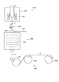
- FIG. 1 is a schematic configuration diagram showing an overall configuration of an optical fiber manufacturing apparatus 1000 used in an optical fiber manufacturing method according to an embodiment of the present invention.
- the optical fiber manufacturing apparatus 1000 includes a drawing furnace 100, a resin coating apparatus 200, an ultraviolet irradiation apparatus 300, and a winding apparatus 400.
- the heater 110 provided in the drawing furnace 100 heats the lower end of the optical fiber preform P to about 2000 ° C.
- the lower end of the optical fiber preform P softened by the heating of the heater 110 is configured to be stretched by the subsequent winding device 400.
- Outer diameter of the optical fiber F 1 produced by drawing furnace 100 is adjusted by the winding speed of the temperature and take-up device 400 of the heater 110.
- the optical fiber manufacturing apparatus 1000 shown in FIG. 1 has a wet-on-wet system configuration.
- the embodiment of the present invention is not limited to the wet-on-wet optical fiber manufacturing apparatus 1000. Even in the case of the wet-on-dry optical fiber manufacturing apparatus 1000, at least one of a set of a plurality of stages of the resin coating apparatus 200 and the ultraviolet irradiation apparatus 300, and preferably all sets.
- the embodiment of the present invention can be applied to the above.
- an embodiment of the present invention will be described using the configuration of an optical fiber manufacturing apparatus 1000 that includes only one set of a resin coating device 200 and an ultraviolet irradiation device 300. Shall.
- the resin coating apparatus 200 is configured such that an optical fiber F 1 manufactured by a drawing furnace 100 passes through the inside.
- Optical fiber F 1 when passing through the interior of the resin coating device 200, an ultraviolet curable resin for the primary layer, and / or an ultraviolet curable resin for the secondary is applied.
- the ultraviolet curable resin may contain, for example, a dilution monomer, a photosensitizer, a silane coupling agent, a chain transfer agent, and various additives in addition to the oligomer and the photopolymerization initiator.
- a dilution monomer monofunctional (meth) acrylate or polyfunctional (meth) acrylate is used.
- the dilution monomer means a monomer for diluting the ultraviolet curable resin.
- 2,4,6-trimethylbenzoyldiphenylphosphine oxide bis (2,4,6-trimethylbenzoyl) -phenylphosphine oxide, bis (2,6-dimethoxybenzoyl) -2,4,4, which are acylphosphine oxide types And -trimethyl-pentylphosphine oxide.
- examples of commercially available products include Irgacure 819, Lucirin TPO, Lucirin TPO-L, and Irgacure 2100 (trade name, manufactured by BASF Japan Ltd.).
- the inert gas introduction pipe 331 is for filling the inside of the transparent pipe 310 with an inert gas.
- an ultraviolet curable resin when cured in an atmosphere having a high oxygen (O 2 ) concentration, it reacts with oxygen and becomes insufficiently cured.
- an inert gas is supplied from the inert gas introduction pipe 331 to the inside of the transparent pipe 310 so that the inside of the transparent pipe 310 has an atmosphere having a low oxygen concentration.
- the type of inert gas is not limited as long as it is inert to the optical fiber F 1 and the ultraviolet curable resin applied to the optical fiber F 1, but it is convenient to use nitrogen (N 2 ).
- the optical fiber F 1 in which the ultraviolet curable resin applied to the outer periphery by the ultraviolet irradiation device 300 is cured is wound around the winding device 400 as an optical fiber strand F 2 .
- the winding device 400 includes guide rollers 410 and 420 and a winding drum 430.
- the illustrated example of the winding device 400 is one configuration example, and the number and arrangement of rollers can be changed. As described above, the winding device 400 controls the outer diameter of the optical fiber F 1 manufactured in the drawing furnace 100 by adjusting the speed at which the optical fiber F 2 is wound.
- the first to sixth ultraviolet irradiation units 321a to 326a are arranged differently with respect to the angle in the circumferential direction with the traveling direction of the optical fiber as an axis. Specifically, with reference to the angle of the first ultraviolet irradiation unit 321a, the second to sixth ultraviolet irradiation units 322a to 326a have angles of 20 °, 40 °, 60 °, 80 °, and 100 °, respectively. Has been changed.
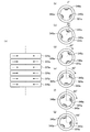
- FIG. 3 is a diagram illustrating a configuration of the ultraviolet irradiation unit and the semiconductor ultraviolet light emitting element according to the second embodiment.
- the ultraviolet irradiation unit according to the second embodiment can also be applied as the plurality of ultraviolet irradiation units 320 in the ultraviolet irradiation apparatus 300 described above.
- the description of the optical fiber is omitted, but the downward direction on the paper corresponds to the traveling direction of the optical fiber, and the straight line indicated by the alternate long and short dash line corresponds to the traveling position of the optical fiber. is doing. Further, since the optical fiber is configured to pass through the center of the circle where the semiconductor ultraviolet light emitting element 340b is arranged, the traveling position of the optical fiber is a cylindrical surface defined by the arrangement position of the semiconductor ultraviolet light emitting element 340b. Coincides with the central axis.
- the first to fourth ultraviolet irradiation units 321b to 324b are arranged differently with respect to the angle in the circumferential direction about the traveling direction of the optical fiber. Specifically, with the angle of the first ultraviolet irradiation unit 321b as a reference, the second to fourth ultraviolet irradiation units 322b to 324b change the angles at 22.5 °, 45 °, and 67.5 °, respectively. It has been.
- the arrows described in the first to fourth ultraviolet irradiation units 321b to 324b shown in FIG. 3A indicate the irradiation direction of the ultraviolet rays emitted from the semiconductor ultraviolet light emitting element 340b. That is, the semiconductor ultraviolet light emitting element 340b included in the first to fourth ultraviolet irradiation units 321b to 324b irradiates ultraviolet rays perpendicular to the axis indicating the traveling direction of the optical fiber.
- the ultraviolet irradiation unit according to the third embodiment includes first to fifth ultraviolet irradiation units 321c to 325c that irradiate ultraviolet curable resin with ultraviolet rays.
- the first to fifth ultraviolet irradiation units 321c to 325c are the same type units in which three semiconductor ultraviolet light emitting elements 340c are arranged on the circumference of the same circle.
- these first to fifth ultraviolet irradiation units 321c to 325c are arranged in the traveling direction of the optical fiber so that the optical fiber passes through the center of the circle.
- the optical fiber is not shown in FIG. 4A, the downward direction on the paper corresponds to the traveling direction of the optical fiber, and the straight line indicated by the alternate long and short dash line corresponds to the traveling position of the optical fiber. is doing. Further, since the optical fiber is configured to pass through the center of the circle where the semiconductor ultraviolet light emitting element 340c is arranged, the traveling position of the optical fiber is a cylindrical surface defined by the arrangement position of the semiconductor ultraviolet light emitting element 340c. Coincides with the central axis.
- the first to fifth ultraviolet irradiation units 321c to 325c are arranged differently with respect to the angle in the circumferential direction about the traveling direction of the optical fiber. Specifically, with reference to the angle of the first ultraviolet irradiation unit 321c, the angles of the second to fifth ultraviolet irradiation units 322c to 325c can be changed by 24 °, 48 °, 72 °, and 96 °, respectively. ing.
- the arrows described in the first to fifth ultraviolet irradiation units 321c to 325c shown in FIG. 4A indicate the irradiation direction of the ultraviolet rays emitted from the semiconductor ultraviolet light emitting element 340c. That is, the semiconductor ultraviolet light emitting element 340c included in the first to fifth ultraviolet irradiation units 321c to 325c is tilted so as to irradiate ultraviolet rays toward one point on the axis indicating the traveling direction of the optical fiber, and the ultraviolet rays are emitted. It is attached to the irradiation unit.
- the semiconductor ultraviolet light emitting element 340c in an inclined manner as described above, the illuminance of ultraviolet rays irradiated on the ultraviolet curable resin is increased, and the curing of the ultraviolet curable resin is promoted. .
- the ultraviolet irradiation unit according to the fourth embodiment includes first to sixth ultraviolet irradiation units 321d to 326d that irradiate ultraviolet curable resin with ultraviolet rays and a deep ultraviolet irradiation unit 350d that irradiates deep ultraviolet rays. It is configured.
- the first to sixth ultraviolet irradiation units 321d to 326d are the same type units in which three semiconductor ultraviolet light emitting elements 340d are arranged on the circumference of the same circle.
- the first to sixth ultraviolet irradiation units 321d to 326d are arranged in the traveling direction of the optical fiber so that the optical fiber passes through the center of the circle.
- the deep ultraviolet irradiation unit 350d is disposed in a front part (upward in the drawing) than the first ultraviolet irradiation unit 321d.
- the deep ultraviolet irradiation unit 350d is provided with semiconductor ultraviolet light emitting elements that emit deep ultraviolet rays, for example, in the same manner as the first ultraviolet irradiation unit 321d.
- Deep ultraviolet rays (for example, wavelengths of 200 nm to 350 nm) have a shorter wavelength than normal ultraviolet rays (for example, wavelengths of 365 nm to 405 nm), and thus act on the ultraviolet curable resin in a layer shallower than the depth at which normal ultraviolet rays reach. Therefore, disposing the deep ultraviolet irradiation unit 350d in the front stage part of the first ultraviolet irradiation unit 321d causes the layer of the ultraviolet curable resin close to the surface to be cured first.
- the ultraviolet curable resin when the ultraviolet curable resin is cured in an atmosphere having a high oxygen concentration, the ultraviolet curable resin reacts with oxygen to be insufficiently cured, so that an inert gas is introduced so that the ultraviolet curable resin does not react with oxygen.
- the deep ultraviolet irradiation unit 350d is disposed in the front part of the first ultraviolet irradiation unit 321d, and the ultraviolet curable resin of the layer close to the surface that is more likely to react with oxygen is cured first, thereby contributing to the improvement of the surface quality. .
- the ultraviolet irradiation unit according to the fourth embodiment is obtained by adding the deep ultraviolet irradiation unit 350d to the ultraviolet irradiation unit according to the first embodiment. Therefore, the ultraviolet irradiation unit according to the fourth embodiment inherits the functions and effects of the ultraviolet irradiation unit according to the first embodiment as they are.
- FIG. 6 is a diagram illustrating a configuration of the ultraviolet irradiation unit and the semiconductor ultraviolet light emitting element according to the fifth embodiment.
- the ultraviolet irradiation unit according to the fifth embodiment can also be applied as the plurality of ultraviolet irradiation units 320 in the ultraviolet irradiation apparatus 300 described above.
- the ultraviolet irradiation unit according to the fifth embodiment includes first to fourth ultraviolet irradiation units 321e to 324e that irradiate ultraviolet curable resin with ultraviolet rays and a deep ultraviolet irradiation unit 350e that irradiates deep ultraviolet rays. It is configured.
- the first to fourth ultraviolet irradiation units 321e to 324e are the same type units in which four semiconductor ultraviolet light emitting elements 340e are arranged on the circumference of the same circle.
- the first to fourth ultraviolet irradiation units 321e to 324e are arranged in the traveling direction of the optical fiber so that the optical fiber passes through the center of the circle.
- the deep ultraviolet irradiation unit 350e is arranged in a front stage (upward in the drawing) than the first ultraviolet irradiation unit 321e.
- the deep ultraviolet irradiation unit 350e has the same configuration as the deep ultraviolet irradiation unit 350d in the fourth embodiment.
- disposing the deep ultraviolet irradiation unit 350e in the front stage portion of the first ultraviolet irradiation unit 321e cures the ultraviolet curable resin in a layer close to the surface that is more likely to react with oxygen first. This contributes to improving the surface quality.
- the ultraviolet irradiation unit according to the fifth embodiment is obtained by adding the deep ultraviolet irradiation unit 350e to the ultraviolet irradiation unit according to the second embodiment. Therefore, the ultraviolet irradiation unit according to the fifth embodiment inherits the functions and effects of the ultraviolet irradiation unit according to the second embodiment as they are.
- FIG. 7 is a diagram illustrating a configuration of the ultraviolet irradiation unit and the semiconductor ultraviolet light emitting element according to the sixth embodiment.
- the ultraviolet irradiation unit according to the sixth embodiment can also be applied as the plurality of ultraviolet irradiation units 320 in the ultraviolet irradiation apparatus 300 described above.
- the ultraviolet irradiation unit according to the sixth embodiment includes first to fifth ultraviolet irradiation units 321f to 325f for irradiating ultraviolet curable resin with ultraviolet rays and a deep ultraviolet irradiation unit 350f for irradiating deep ultraviolet rays. It is configured.
- the first to fifth ultraviolet irradiation units 321f to 325f are the same type units in which three semiconductor ultraviolet light emitting elements 340f are arranged on the circumference of the same circle.
- the first to fifth ultraviolet irradiation units 321f to 325f are arranged in the traveling direction of the optical fiber so that the optical fiber passes through the center of the circle.
- the deep ultraviolet irradiation unit 350f is disposed in a front part (upward in the drawing) than the first ultraviolet irradiation unit 321f.
- the deep ultraviolet irradiation unit 350f has the same configuration as the deep ultraviolet irradiation unit 350d in the fourth embodiment.
- disposing the deep ultraviolet irradiation unit 350f in front of the first ultraviolet irradiation unit 321f allows the ultraviolet curing resin of the layer closer to the surface that is more likely to react with oxygen to be cured first. This contributes to improving the surface quality.
- the ultraviolet irradiation unit according to the sixth embodiment is obtained by adding the deep ultraviolet irradiation unit 350f to the ultraviolet irradiation unit according to the third embodiment. Therefore, the ultraviolet irradiation unit according to the sixth embodiment inherits the functions and effects of the ultraviolet irradiation unit according to the third embodiment as they are.
- FIG. 8 is a diagram showing a configuration of an ultraviolet irradiation unit and a semiconductor ultraviolet light emitting element according to a comparative example.
- the comparative example is used in a verification experiment showing the effect of the present invention described later.
- the ultraviolet irradiation unit which concerns on a comparative example can also be applied as the several ultraviolet irradiation unit 320 in the ultraviolet irradiation apparatus 300 demonstrated above.
- the ultraviolet irradiation unit according to the comparative example is composed of first to sixth ultraviolet irradiation units 321g to 326g that irradiate the ultraviolet curable resin with ultraviolet rays.
- the first to sixth ultraviolet irradiation units 321g to 326g are the same type units in which three semiconductor ultraviolet light emitting elements 340g are arranged on the circumference of the same circle.
- the first to sixth ultraviolet irradiation units 321g to 326g are arranged in the traveling direction of the optical fiber so that the optical fiber passes through the center of the circle.
- the configurations of the ultraviolet irradiation unit and the semiconductor ultraviolet light emitting element according to the comparative example are substantially the same as the configurations of the ultraviolet irradiation unit and the semiconductor ultraviolet light emitting element according to the first embodiment, but in the comparative example, FIG.
- the first to sixth ultraviolet irradiation units 321g to 326g have the same arrangement with respect to the angle in the circumferential direction about the traveling direction of the optical fiber.
- the semiconductor ultraviolet light emitting element 340g included in the first to sixth ultraviolet irradiation units 321g to 326g irradiates ultraviolet rays perpendicular to the axis indicating the traveling direction of the optical fiber.
- a semiconductor ultraviolet light emitting element is disposed in the unit itself.
- a configuration in which ultraviolet rays emitted from an ultraviolet light source are guided by an optical fiber or the like may be provided at a position where the ultraviolet rays are irradiated toward the ultraviolet curable resin.
- Table 1 listed below is a table showing results of experiments for verifying the effects of the method for manufacturing an optical fiber and the ultraviolet irradiation device according to the embodiment of the present invention.
- the verification experiment described in Table 1 verified the characteristics of the optical fiber when the optical fiber was manufactured using the ultraviolet irradiation apparatus to which the configurations described in Examples 1 to 6 and the comparative example were applied. It is.
- the embodiment of the present invention is applied only to the secondary layer in order to easily verify the effect.
- the photoinitiator used for the ultraviolet curable resin of the secondary layer is Irgacure 184 (BASF Japan Ltd.).
- the reduction rate of power consumption means the reduction rate of power consumption when compared with the comparative example.
- the determination of the presence or absence of waviness is made by measuring the length of the manufactured optical fiber in a state where tension is applied and in a state where it is not applied, and the length of the optical fiber measured in the state where tension is applied is 30 m. When the length of the optical fiber measured in a state where no tension is applied is contracted by 5 cm or more, it is determined that there is undulation.
- the state where tension is applied is the tension when the optical fiber is drawn out from the bobbin, and 50 g is used.
- FIG. 9 is a schematic diagram showing an outline of the performed knot test. As shown in FIG. 9, a single loop is formed with the manufactured optical fiber F 3 , and the optical fiber F 3 is sequentially passed through the loop as shown in FIG. A circle having a diameter of about 7 cm that makes contact with itself is made, and both ends of the optical fiber are pulled at a speed of 5 mm / min by a tensile tester. What measured the load (N) at this time is used.
- the cable loss is a loss related to the transmission of light having a wavelength of 1.55 ⁇ m in a loose tube type optical fiber cable created using an optical fiber, and the allowable range is 0.230 dB / km or less.
- FIG. 10 is a cross-sectional view showing the structure of a loose tube type optical fiber cable, and the cable loss was measured using the loose tube type optical fiber cable.
- the loose tube type optical fiber cable F 4 includes a tension member 41, an optical fiber colored core wire 42, a loose tube 43, a jelly 44, and a sheath 45.
- the tension member 41 is made of metal or plastic.
- a plurality of loose tubes 43 made of metal or plastic are provided on the side surface of the tension member 41 through the optical fiber colored core wire 42. These loose tubes 43 are covered with a sheath 45 made of plastic, and a gap between them is filled with a jelly 44.
- the value of 2.5% modulus was measured as follows. First, an optical fiber manufactured by a manufacturing method using an ultraviolet irradiation device to which the configurations of Examples 1 to 6 and the comparative example are applied is immersed in liquid nitrogen, and a glass core wire is used using a coating removal jig at the liquid nitrogen temperature. And the coating layer is formed into a tube shape. And this tube-shaped optical fiber coating layer 50mm length was made into the sample, and 2.5% modulus was measured by 25 mm of distances between marked lines based on this sample based on JISK7161.
- the optical fiber manufactured using the ultraviolet irradiation apparatus to which the configurations of Examples 1 to 6 are applied does not generate undulation, but the ultraviolet irradiation apparatus to which the configuration of the comparative example is applied. Waves are generated in the optical fiber produced by using the optical fiber. This indicates that in the ultraviolet irradiation apparatus to which the configurations of Examples 1 to 6 are applied, the ultraviolet rays are uniformly irradiated in the circumferential direction of the optical fiber, and a good coating is formed.
- the measurement result of knot test is remarkably improved in the optical fiber manufactured using the ultraviolet irradiation apparatus to which the configurations of Examples 4 to 6 are applied.
- the surface quality of the coating is improved by first curing the ultraviolet curable resin of the layer close to the surface using the deep ultraviolet irradiation unit.
- the optical fiber manufactured using the ultraviolet irradiation apparatus to which the configurations of Examples 1 to 6 are applied has a good cable loss value.
- the optical fiber manufactured using the ultraviolet irradiation apparatus to which the configurations of Examples 1 to 6 are applied is manufactured using the ultraviolet irradiation apparatus to which the configuration of the comparative example is applied. Compared with an optical fiber, 2.5% modulus is high. This indicates that in the ultraviolet irradiation apparatus to which the configurations of Examples 1 to 6 were applied, the ultraviolet curable resin was sufficiently irradiated with ultraviolet rays and a good coating was formed.
- the power consumption of the ultraviolet irradiation device to which the configurations of Examples 2, 3, 5, and 6 are applied is less than that of the ultraviolet irradiation device to which the configuration of the comparative example is applied. This is because the number of semiconductor ultraviolet light emitting elements used is smaller in the ultraviolet irradiation device to which the configurations of Examples 2, 3, 5, and 6 are applied than in the ultraviolet irradiation device to which the configuration of the comparative example is applied.
- a deep ultraviolet semiconductor ultraviolet light emitting element is also used, but the deep ultraviolet semiconductor ultraviolet light emitting element is compared with a normal semiconductor ultraviolet light emitting element. Since power consumption is small, the effect is negligibly small.
- the semiconductor ultraviolet light emitting element is arranged so as to irradiate ultraviolet rays toward one point on the axis indicating the traveling direction of the optical fiber. It will be described how this configuration contributes to the curing of the coating.
- FIG. 11 is a graph showing the relationship between the illuminance (I) of the ultraviolet rays irradiated to the ultraviolet curable resin and the 2.5% modulus (G). The measurement result shown in FIG. 11 is obtained by the following measurement.
- a base material made of quartz glass is prepared, and a secondary UV curable resin is spin-coated at a thickness of 50 ⁇ m.
- the ultraviolet curable resin for secondary is the same as the resin used in the comparative experiment of the above-described embodiment.
- the substrate coated with the secondary UV curable resin is placed in a purge box to create a nitrogen atmosphere, and the illuminance and speed are adjusted with a conveyor type UV irradiation device so as to obtain a predetermined integrated light amount, and UV (365 nm) is irradiated. , Cure the resin.
- the cured secondary UV curable resin is peeled off from the base material and cut into a strip of 6 mm width to obtain a sample having a length of 50 mm or more. This sample is measured for 2.5% modulus (elastic modulus) in accordance with JIS K 7161 with a distance between marked lines of 25 mm.
- the semiconductor ultraviolet light emitting element is configured to irradiate ultraviolet rays toward one point on the axis indicating the traveling direction of the optical fiber. The illuminance of the ultraviolet rays irradiated to the surface is increased, so that a better coating can be formed.
- the semiconductor ultraviolet light emitting element provided in the ultraviolet irradiation unit is disposed on a spiral with the traveling direction of the optical fiber as an axis, but it is not always necessary to have a spiral arrangement. It is also possible to arrange the semiconductor ultraviolet light emitting elements differently with respect to the angle in the circumferential direction about the traveling direction of the optical fiber.
- the method for manufacturing an optical fiber and the ultraviolet irradiation device according to the present invention are useful for manufacturing an optical fiber.
- SYMBOLS 1000 Optical fiber manufacturing apparatus 100 Drawing furnace 110 Heater 200 Resin coating apparatus 300 Ultraviolet irradiation apparatus 310 Transparent tube 320,321-326 Ultraviolet irradiation unit 331 Inert gas introduction pipe 340 Semiconductor ultraviolet light emitting element 350 Deep ultraviolet irradiation unit 400 Winding Take-up device 410, 420 Guide roller 430 Take-up drum 41 Tension member 42 Optical fiber colored core wire 43 Loose tube 44 Jelly 45 Sheath
Landscapes
- Chemical & Material Sciences (AREA)
- Life Sciences & Earth Sciences (AREA)
- Engineering & Computer Science (AREA)
- Chemical Kinetics & Catalysis (AREA)
- General Chemical & Material Sciences (AREA)
- Materials Engineering (AREA)
- Organic Chemistry (AREA)
- Physics & Mathematics (AREA)
- General Life Sciences & Earth Sciences (AREA)
- Geochemistry & Mineralogy (AREA)
- Health & Medical Sciences (AREA)
- Toxicology (AREA)
- Mechanical Engineering (AREA)
- Oral & Maxillofacial Surgery (AREA)
- Thermal Sciences (AREA)
- Electromagnetism (AREA)
- Metallurgy (AREA)
- General Engineering & Computer Science (AREA)
- General Physics & Mathematics (AREA)
- Optics & Photonics (AREA)
- Surface Treatment Of Glass Fibres Or Filaments (AREA)
- Optical Fibers, Optical Fiber Cores, And Optical Fiber Bundles (AREA)
- Coating Apparatus (AREA)
Abstract
L'invention concerne un procédé de production de fibres optiques par irradiation d'une résine durcissable aux ultraviolets appliquée sur la périphérie extérieure d'une fibre optique par de la lumière ultraviolette émise par un élément électroluminescent ultraviolet semi-conducteur pour durcir la résine durcissable aux ultraviolets. Dans le procédé de production de fibres optiques par irradiation de la résine durcissable aux ultraviolets appliquée sur la périphérie extérieure d'une fibre optique par de la lumière ultraviolette, un dispositif d'irradiation de lumière ultraviolette est utilisé, dans lequel une pluralité d'unités d'irradiation de lumière ultraviolette, chacune présentant une pluralité de positions disposées sur la circonférence du même cercle pour émettre de la lumière ultraviolette vers la résine durcissable aux ultraviolets, sont alignées dans la direction de déplacement de la fibre optique de manière telle que la fibre optique passe à travers le centre du cercle, et au moins deux unités parmi la pluralité d'unités d'irradiation de lumière ultraviolette sont disposées différemment en termes d'angle dans la direction circonférentielle par rapport à la direction de déplacement de la fibre optique servant d'axe.
Priority Applications (5)
| Application Number | Priority Date | Filing Date | Title |
|---|---|---|---|
| EP16878968.3A EP3395776B1 (fr) | 2015-12-25 | 2016-12-22 | Procédé de production de fibre optique et dispositif d'irradiation de lumière ultraviolette |
| CN201680074451.7A CN108367977B (zh) | 2015-12-25 | 2016-12-22 | 光纤线材的制造方法以及紫外线照射装置 |
| JP2017520569A JP6266172B2 (ja) | 2015-12-25 | 2016-12-22 | 光ファイバ素線の製造方法および紫外線照射装置 |
| US16/001,985 US11073258B2 (en) | 2015-12-25 | 2018-06-07 | Ultraviolet irradiation device including circular irradiation units that focus light on a single point |
| US17/324,645 US11846407B2 (en) | 2015-12-25 | 2021-05-19 | Bare optical fiber manufacturing method |
Applications Claiming Priority (2)
| Application Number | Priority Date | Filing Date | Title |
|---|---|---|---|
| JP2015-254793 | 2015-12-25 | ||
| JP2015254793 | 2015-12-25 |
Related Child Applications (1)
| Application Number | Title | Priority Date | Filing Date |
|---|---|---|---|
| US16/001,985 Continuation US11073258B2 (en) | 2015-12-25 | 2018-06-07 | Ultraviolet irradiation device including circular irradiation units that focus light on a single point |
Publications (1)
| Publication Number | Publication Date |
|---|---|
| WO2017111082A1 true WO2017111082A1 (fr) | 2017-06-29 |
Family
ID=59090503
Family Applications (1)
| Application Number | Title | Priority Date | Filing Date |
|---|---|---|---|
| PCT/JP2016/088486 WO2017111082A1 (fr) | 2015-12-25 | 2016-12-22 | Procédé de production de fibre optique et dispositif d'irradiation de lumière ultraviolette |
Country Status (5)
| Country | Link |
|---|---|
| US (2) | US11073258B2 (fr) |
| EP (1) | EP3395776B1 (fr) |
| JP (1) | JP6266172B2 (fr) |
| CN (1) | CN108367977B (fr) |
| WO (1) | WO2017111082A1 (fr) |
Families Citing this family (2)
| Publication number | Priority date | Publication date | Assignee | Title |
|---|---|---|---|---|
| CN109127326A (zh) * | 2018-09-20 | 2019-01-04 | 徐亚琴 | 一种光纤带固化设备 |
| CN109262918A (zh) * | 2018-09-20 | 2019-01-25 | 徐亚琴 | 一种光纤带固化优化方法 |
Citations (13)
| Publication number | Priority date | Publication date | Assignee | Title |
|---|---|---|---|---|
| JPS6158840A (ja) * | 1984-08-29 | 1986-03-26 | Furukawa Electric Co Ltd:The | 光フアイバ用被覆層の硬化装置 |
| JPS63130313A (ja) * | 1986-11-21 | 1988-06-02 | Furukawa Electric Co Ltd:The | 紫外線照射装置 |
| US20050222295A1 (en) * | 2003-01-09 | 2005-10-06 | Con-Trol-Cure, Inc. | UV Curing System and Process with Increased Light Intensity |
| JP2010117526A (ja) | 2008-11-12 | 2010-05-27 | Sumitomo Electric Ind Ltd | 紫外線照射装置及び光ファイバの被覆形成方法 |
| JP2010117527A (ja) | 2008-11-12 | 2010-05-27 | Sumitomo Electric Ind Ltd | 紫外線照射装置及び光ファイバの被覆形成方法 |
| JP2010117530A (ja) | 2008-11-12 | 2010-05-27 | Sumitomo Electric Ind Ltd | 紫外線照射装置及び光ファイバの被覆形成方法 |
| JP2010117525A (ja) | 2008-11-12 | 2010-05-27 | Sumitomo Electric Ind Ltd | 紫外線照射装置及び光ファイバの被覆形成方法 |
| JP2010117531A (ja) | 2008-11-12 | 2010-05-27 | Sumitomo Electric Ind Ltd | 紫外線照射装置及び光ファイバの被覆形成方法 |
| CN103319100A (zh) * | 2013-06-19 | 2013-09-25 | 长飞光纤光缆有限公司 | 一种光纤涂层紫外固化设备及方法 |
| US20140097361A1 (en) * | 2008-12-31 | 2014-04-10 | Draka Comteq, B.V. | Method for Curing Glass-Fiber Coatings |
| JP2014142631A (ja) * | 2012-12-28 | 2014-08-07 | Daicel Corp | 高分子光ファイバーの製造方法及び該方法により製造された高分子光ファイバー |
| CN105084783A (zh) * | 2015-09-21 | 2015-11-25 | 长飞光纤光缆股份有限公司 | 一种光纤着色固化设备 |
| JP2016004927A (ja) * | 2014-06-18 | 2016-01-12 | 株式会社オーク製作所 | 紫外線照射装置 |
Family Cites Families (19)
| Publication number | Priority date | Publication date | Assignee | Title |
|---|---|---|---|---|
| JPS5895395A (ja) | 1981-11-30 | 1983-06-06 | 星野楽器株式会社 | ハイフアツトスタンド用シンバル止め具 |
| JPH066971Y2 (ja) | 1987-02-20 | 1994-02-23 | 日産自動車株式会社 | 車両用接着式ウインドウパネルのダムラバ− |
| US5636307A (en) * | 1988-05-23 | 1997-06-03 | The United States Of America As Represented By The Secretary Of The Navy | Fiber optic microcable produced with radiation cured composite |
| TW297798B (fr) * | 1989-03-15 | 1997-02-11 | Sumitomo Electric Industries | |
| US5219623A (en) * | 1990-03-09 | 1993-06-15 | At&T Bell Laboratories | Methods of producing an article which includes a light energy cured coating material |
| CN1157610C (zh) * | 1997-01-15 | 2004-07-14 | 阿尔卡塔尔公司 | 固化光纤的方法和设备 |
| CN1193745C (zh) | 2001-02-27 | 2005-03-23 | 国家医药管理局上海医药工业研究院 | 一种鼻用鲑降钙素粉末吸入剂及制备方法 |
| JP2005104108A (ja) * | 2003-10-02 | 2005-04-21 | Matsushita Electric Ind Co Ltd | インクジェット式記録装置及びインクジェット記録方法 |
| JP2007261919A (ja) * | 2006-03-30 | 2007-10-11 | Furukawa Electric Co Ltd:The | 光ファイバの被覆装置 |
| US7959282B2 (en) * | 2007-12-20 | 2011-06-14 | Summit Business Products, Inc. | Concentrated energy source |
| US8277138B2 (en) * | 2008-04-30 | 2012-10-02 | Adastra Technologies, Inc. | Machine and method for rapid application and curing of thin ultraviolet light curable coatings |
| JP5250630B2 (ja) * | 2008-12-19 | 2013-07-31 | 株式会社フジクラ | 光ファイバ母材の製造方法 |
| GB2491603B (en) * | 2011-06-07 | 2013-08-21 | Univ Dublin City | Capillary column curing system |
| WO2014009939A1 (fr) * | 2012-07-12 | 2014-01-16 | Hewlett-Packard Industrial Printing Ltd. | Source d'éclairage à del |
| JPWO2014041940A1 (ja) * | 2012-09-14 | 2016-08-18 | 富士フイルム株式会社 | 硬化性組成物および画像形成方法 |
| JP6343944B2 (ja) * | 2014-01-30 | 2018-06-20 | セイコーエプソン株式会社 | インクジェット記録方法及び記録装置 |
| JP5851636B1 (ja) * | 2015-02-10 | 2016-02-03 | 株式会社フジクラ | 光ファイバ素線の製造方法、制御装置および製造装置 |
| WO2017014161A1 (fr) * | 2015-07-17 | 2017-01-26 | 富士フイルム株式会社 | Composition durcissable |
| CN105060739B (zh) * | 2015-07-31 | 2018-06-12 | 长飞光纤光缆股份有限公司 | 一种光强可调的光纤涂层紫外固化设备 |
-
2016
- 2016-12-22 JP JP2017520569A patent/JP6266172B2/ja active Active
- 2016-12-22 CN CN201680074451.7A patent/CN108367977B/zh active Active
- 2016-12-22 EP EP16878968.3A patent/EP3395776B1/fr active Active
- 2016-12-22 WO PCT/JP2016/088486 patent/WO2017111082A1/fr active Application Filing
-
2018
- 2018-06-07 US US16/001,985 patent/US11073258B2/en active Active
-
2021
- 2021-05-19 US US17/324,645 patent/US11846407B2/en active Active
Patent Citations (13)
| Publication number | Priority date | Publication date | Assignee | Title |
|---|---|---|---|---|
| JPS6158840A (ja) * | 1984-08-29 | 1986-03-26 | Furukawa Electric Co Ltd:The | 光フアイバ用被覆層の硬化装置 |
| JPS63130313A (ja) * | 1986-11-21 | 1988-06-02 | Furukawa Electric Co Ltd:The | 紫外線照射装置 |
| US20050222295A1 (en) * | 2003-01-09 | 2005-10-06 | Con-Trol-Cure, Inc. | UV Curing System and Process with Increased Light Intensity |
| JP2010117525A (ja) | 2008-11-12 | 2010-05-27 | Sumitomo Electric Ind Ltd | 紫外線照射装置及び光ファイバの被覆形成方法 |
| JP2010117527A (ja) | 2008-11-12 | 2010-05-27 | Sumitomo Electric Ind Ltd | 紫外線照射装置及び光ファイバの被覆形成方法 |
| JP2010117530A (ja) | 2008-11-12 | 2010-05-27 | Sumitomo Electric Ind Ltd | 紫外線照射装置及び光ファイバの被覆形成方法 |
| JP2010117526A (ja) | 2008-11-12 | 2010-05-27 | Sumitomo Electric Ind Ltd | 紫外線照射装置及び光ファイバの被覆形成方法 |
| JP2010117531A (ja) | 2008-11-12 | 2010-05-27 | Sumitomo Electric Ind Ltd | 紫外線照射装置及び光ファイバの被覆形成方法 |
| US20140097361A1 (en) * | 2008-12-31 | 2014-04-10 | Draka Comteq, B.V. | Method for Curing Glass-Fiber Coatings |
| JP2014142631A (ja) * | 2012-12-28 | 2014-08-07 | Daicel Corp | 高分子光ファイバーの製造方法及び該方法により製造された高分子光ファイバー |
| CN103319100A (zh) * | 2013-06-19 | 2013-09-25 | 长飞光纤光缆有限公司 | 一种光纤涂层紫外固化设备及方法 |
| JP2016004927A (ja) * | 2014-06-18 | 2016-01-12 | 株式会社オーク製作所 | 紫外線照射装置 |
| CN105084783A (zh) * | 2015-09-21 | 2015-11-25 | 长飞光纤光缆股份有限公司 | 一种光纤着色固化设备 |
Also Published As
| Publication number | Publication date |
|---|---|
| CN108367977A (zh) | 2018-08-03 |
| US20210270448A1 (en) | 2021-09-02 |
| EP3395776A1 (fr) | 2018-10-31 |
| US11073258B2 (en) | 2021-07-27 |
| EP3395776B1 (fr) | 2023-05-03 |
| EP3395776A4 (fr) | 2019-06-05 |
| JP6266172B2 (ja) | 2018-01-24 |
| JPWO2017111082A1 (ja) | 2017-12-28 |
| US20180282209A1 (en) | 2018-10-04 |
| US11846407B2 (en) | 2023-12-19 |
| CN108367977B (zh) | 2021-06-18 |
Similar Documents
| Publication | Publication Date | Title |
|---|---|---|
| JP3952620B2 (ja) | フォトイニシエータ調整形光ファイバおよび光ファイバリボンおよびこれらの製造方法 | |
| US11846407B2 (en) | Bare optical fiber manufacturing method | |
| JP2950264B2 (ja) | 光ファイバテープ心線の製造方法 | |
| JP7536670B2 (ja) | 光ファイバ心線の製造方法 | |
| JP6576995B2 (ja) | 光ファイバ素線の製造方法及び製造装置 | |
| JPH01148733A (ja) | 光ファイバの製造方法および装置 | |
| WO2022191097A1 (fr) | Fil de cœur coloré de fibre optique, ruban de fibre optique, câble d'assemblage de fibres monocoœur, câble de type ruban, et procédé de fabrication associé | |
| US6419743B1 (en) | Apparatus and method for passing multiple fibers through a small zone of high intensity radiant energy | |
| JP2017145146A (ja) | 光ファイバ素線の製造方法 | |
| JP2021031366A (ja) | 着色光ファイバの製造方法 | |
| JP6582815B2 (ja) | 光ファイバの製造方法 | |
| JP6561106B2 (ja) | 光ファイバ素線の製造方法及び製造装置 | |
| JP6622272B2 (ja) | 光ファイバ素線の製造方法及び光ファイバ素線の製造装置 | |
| JP3858895B2 (ja) | 光ファイバ心線およびその製造方法 | |
| JP2021534069A (ja) | 光ファイバ硬化要素 | |
| CN1139820C (zh) | 光纤涂层方法 | |
| US20200369563A1 (en) | Systems and methods for forming optical fiber coatings with reduced defects on moving optical fibers | |
| WO2024029592A1 (fr) | Âme de fibre optique colorée et son procédé de production | |
| WO2022092089A1 (fr) | Fil d'âme de fibre optique coloré, ruban de fibre optique, câble d'assemblage de fibre à âme unique, câble plat et leur procédé de fabrication | |
| WO2022264873A1 (fr) | Fil à cœur de fibre optique coloré, ruban de fibre optique, câble à ruban de fibre optique et procédés de production associés | |
| JP2023502874A (ja) | 低減衰ロール可能な光ファイバリボン | |
| JP2023119763A (ja) | 光ファイバの製造方法 | |
| JP2023081056A (ja) | 光ファイバリボン及び光ファイバリボンの製造方法 | |
| JP2019064854A (ja) | 光ファイバ素線の製造方法及び光ファイバ素線の製造装置 | |
| JP2023081059A (ja) | 光ファイバ着色心線及び光ファイバ着色心線の製造方法 |
Legal Events
| Date | Code | Title | Description |
|---|---|---|---|
| ENP | Entry into the national phase |
Ref document number: 2017520569 Country of ref document: JP Kind code of ref document: A |
|
| 121 | Ep: the epo has been informed by wipo that ep was designated in this application |
Ref document number: 16878968 Country of ref document: EP Kind code of ref document: A1 |
|
| NENP | Non-entry into the national phase |
Ref country code: DE |
|
| WWE | Wipo information: entry into national phase |
Ref document number: 2016878968 Country of ref document: EP |