WO2017111082A1 - Optical fiber production method and ultraviolet light irradiation device - Google Patents
Optical fiber production method and ultraviolet light irradiation device Download PDFInfo
- Publication number
- WO2017111082A1 WO2017111082A1 PCT/JP2016/088486 JP2016088486W WO2017111082A1 WO 2017111082 A1 WO2017111082 A1 WO 2017111082A1 JP 2016088486 W JP2016088486 W JP 2016088486W WO 2017111082 A1 WO2017111082 A1 WO 2017111082A1
- Authority
- WO
- WIPO (PCT)
- Prior art keywords
- ultraviolet
- optical fiber
- ultraviolet irradiation
- light emitting
- semiconductor
- Prior art date
Links
Images


Classifications
-
- F—MECHANICAL ENGINEERING; LIGHTING; HEATING; WEAPONS; BLASTING
- F21—LIGHTING
- F21V—FUNCTIONAL FEATURES OR DETAILS OF LIGHTING DEVICES OR SYSTEMS THEREOF; STRUCTURAL COMBINATIONS OF LIGHTING DEVICES WITH OTHER ARTICLES, NOT OTHERWISE PROVIDED FOR
- F21V15/00—Protecting lighting devices from damage
- F21V15/01—Housings, e.g. material or assembling of housing parts
-
- C—CHEMISTRY; METALLURGY
- C03—GLASS; MINERAL OR SLAG WOOL
- C03C—CHEMICAL COMPOSITION OF GLASSES, GLAZES OR VITREOUS ENAMELS; SURFACE TREATMENT OF GLASS; SURFACE TREATMENT OF FIBRES OR FILAMENTS MADE FROM GLASS, MINERALS OR SLAGS; JOINING GLASS TO GLASS OR OTHER MATERIALS
- C03C25/00—Surface treatment of fibres or filaments made from glass, minerals or slags
- C03C25/10—Coating
- C03C25/24—Coatings containing organic materials
- C03C25/26—Macromolecular compounds or prepolymers
-
- B—PERFORMING OPERATIONS; TRANSPORTING
- B05—SPRAYING OR ATOMISING IN GENERAL; APPLYING FLUENT MATERIALS TO SURFACES, IN GENERAL
- B05C—APPARATUS FOR APPLYING FLUENT MATERIALS TO SURFACES, IN GENERAL
- B05C9/00—Apparatus or plant for applying liquid or other fluent material to surfaces by means not covered by any preceding group, or in which the means of applying the liquid or other fluent material is not important
- B05C9/08—Apparatus or plant for applying liquid or other fluent material to surfaces by means not covered by any preceding group, or in which the means of applying the liquid or other fluent material is not important for applying liquid or other fluent material and performing an auxiliary operation
- B05C9/14—Apparatus or plant for applying liquid or other fluent material to surfaces by means not covered by any preceding group, or in which the means of applying the liquid or other fluent material is not important for applying liquid or other fluent material and performing an auxiliary operation the auxiliary operation involving heating or cooling
-
- B—PERFORMING OPERATIONS; TRANSPORTING
- B29—WORKING OF PLASTICS; WORKING OF SUBSTANCES IN A PLASTIC STATE IN GENERAL
- B29C—SHAPING OR JOINING OF PLASTICS; SHAPING OF MATERIAL IN A PLASTIC STATE, NOT OTHERWISE PROVIDED FOR; AFTER-TREATMENT OF THE SHAPED PRODUCTS, e.g. REPAIRING
- B29C33/00—Moulds or cores; Details thereof or accessories therefor
- B29C33/02—Moulds or cores; Details thereof or accessories therefor with incorporated heating or cooling means
- B29C33/06—Moulds or cores; Details thereof or accessories therefor with incorporated heating or cooling means using radiation, e.g. electro-magnetic waves, induction heating
-
- B—PERFORMING OPERATIONS; TRANSPORTING
- B29—WORKING OF PLASTICS; WORKING OF SUBSTANCES IN A PLASTIC STATE IN GENERAL
- B29C—SHAPING OR JOINING OF PLASTICS; SHAPING OF MATERIAL IN A PLASTIC STATE, NOT OTHERWISE PROVIDED FOR; AFTER-TREATMENT OF THE SHAPED PRODUCTS, e.g. REPAIRING
- B29C35/00—Heating, cooling or curing, e.g. crosslinking or vulcanising; Apparatus therefor
- B29C35/02—Heating or curing, e.g. crosslinking or vulcanizing during moulding, e.g. in a mould
- B29C35/08—Heating or curing, e.g. crosslinking or vulcanizing during moulding, e.g. in a mould by wave energy or particle radiation
- B29C35/0888—Heating or curing, e.g. crosslinking or vulcanizing during moulding, e.g. in a mould by wave energy or particle radiation using transparant moulds
-
- B—PERFORMING OPERATIONS; TRANSPORTING
- B29—WORKING OF PLASTICS; WORKING OF SUBSTANCES IN A PLASTIC STATE IN GENERAL
- B29C—SHAPING OR JOINING OF PLASTICS; SHAPING OF MATERIAL IN A PLASTIC STATE, NOT OTHERWISE PROVIDED FOR; AFTER-TREATMENT OF THE SHAPED PRODUCTS, e.g. REPAIRING
- B29C35/00—Heating, cooling or curing, e.g. crosslinking or vulcanising; Apparatus therefor
- B29C35/02—Heating or curing, e.g. crosslinking or vulcanizing during moulding, e.g. in a mould
- B29C35/08—Heating or curing, e.g. crosslinking or vulcanizing during moulding, e.g. in a mould by wave energy or particle radiation
- B29C35/10—Heating or curing, e.g. crosslinking or vulcanizing during moulding, e.g. in a mould by wave energy or particle radiation for articles of indefinite length
-
- C—CHEMISTRY; METALLURGY
- C03—GLASS; MINERAL OR SLAG WOOL
- C03C—CHEMICAL COMPOSITION OF GLASSES, GLAZES OR VITREOUS ENAMELS; SURFACE TREATMENT OF GLASS; SURFACE TREATMENT OF FIBRES OR FILAMENTS MADE FROM GLASS, MINERALS OR SLAGS; JOINING GLASS TO GLASS OR OTHER MATERIALS
- C03C25/00—Surface treatment of fibres or filaments made from glass, minerals or slags
- C03C25/10—Coating
- C03C25/104—Coating to obtain optical fibres
- C03C25/106—Single coatings
-
- C—CHEMISTRY; METALLURGY
- C03—GLASS; MINERAL OR SLAG WOOL
- C03C—CHEMICAL COMPOSITION OF GLASSES, GLAZES OR VITREOUS ENAMELS; SURFACE TREATMENT OF GLASS; SURFACE TREATMENT OF FIBRES OR FILAMENTS MADE FROM GLASS, MINERALS OR SLAGS; JOINING GLASS TO GLASS OR OTHER MATERIALS
- C03C25/00—Surface treatment of fibres or filaments made from glass, minerals or slags
- C03C25/10—Coating
- C03C25/12—General methods of coating; Devices therefor
-
- C—CHEMISTRY; METALLURGY
- C03—GLASS; MINERAL OR SLAG WOOL
- C03C—CHEMICAL COMPOSITION OF GLASSES, GLAZES OR VITREOUS ENAMELS; SURFACE TREATMENT OF GLASS; SURFACE TREATMENT OF FIBRES OR FILAMENTS MADE FROM GLASS, MINERALS OR SLAGS; JOINING GLASS TO GLASS OR OTHER MATERIALS
- C03C25/00—Surface treatment of fibres or filaments made from glass, minerals or slags
- C03C25/62—Surface treatment of fibres or filaments made from glass, minerals or slags by application of electric or wave energy; by particle radiation or ion implantation
- C03C25/6206—Electromagnetic waves
- C03C25/6226—Ultraviolet
-
- C—CHEMISTRY; METALLURGY
- C23—COATING METALLIC MATERIAL; COATING MATERIAL WITH METALLIC MATERIAL; CHEMICAL SURFACE TREATMENT; DIFFUSION TREATMENT OF METALLIC MATERIAL; COATING BY VACUUM EVAPORATION, BY SPUTTERING, BY ION IMPLANTATION OR BY CHEMICAL VAPOUR DEPOSITION, IN GENERAL; INHIBITING CORROSION OF METALLIC MATERIAL OR INCRUSTATION IN GENERAL
- C23C—COATING METALLIC MATERIAL; COATING MATERIAL WITH METALLIC MATERIAL; SURFACE TREATMENT OF METALLIC MATERIAL BY DIFFUSION INTO THE SURFACE, BY CHEMICAL CONVERSION OR SUBSTITUTION; COATING BY VACUUM EVAPORATION, BY SPUTTERING, BY ION IMPLANTATION OR BY CHEMICAL VAPOUR DEPOSITION, IN GENERAL
- C23C16/00—Chemical coating by decomposition of gaseous compounds, without leaving reaction products of surface material in the coating, i.e. chemical vapour deposition [CVD] processes
- C23C16/44—Chemical coating by decomposition of gaseous compounds, without leaving reaction products of surface material in the coating, i.e. chemical vapour deposition [CVD] processes characterised by the method of coating
- C23C16/54—Apparatus specially adapted for continuous coating
- C23C16/545—Apparatus specially adapted for continuous coating for coating elongated substrates
-
- G—PHYSICS
- G02—OPTICS
- G02B—OPTICAL ELEMENTS, SYSTEMS OR APPARATUS
- G02B6/00—Light guides; Structural details of arrangements comprising light guides and other optical elements, e.g. couplings
- G02B6/44—Mechanical structures for providing tensile strength and external protection for fibres, e.g. optical transmission cables
-
- H—ELECTRICITY
- H05—ELECTRIC TECHNIQUES NOT OTHERWISE PROVIDED FOR
- H05B—ELECTRIC HEATING; ELECTRIC LIGHT SOURCES NOT OTHERWISE PROVIDED FOR; CIRCUIT ARRANGEMENTS FOR ELECTRIC LIGHT SOURCES, IN GENERAL
- H05B1/00—Details of electric heating devices
- H05B1/02—Automatic switching arrangements specially adapted to apparatus ; Control of heating devices
- H05B1/0227—Applications
- H05B1/023—Industrial applications
-
- H—ELECTRICITY
- H05—ELECTRIC TECHNIQUES NOT OTHERWISE PROVIDED FOR
- H05B—ELECTRIC HEATING; ELECTRIC LIGHT SOURCES NOT OTHERWISE PROVIDED FOR; CIRCUIT ARRANGEMENTS FOR ELECTRIC LIGHT SOURCES, IN GENERAL
- H05B45/00—Circuit arrangements for operating light-emitting diodes [LED]
- H05B45/10—Controlling the intensity of the light
-
- A—HUMAN NECESSITIES
- A61—MEDICAL OR VETERINARY SCIENCE; HYGIENE
- A61N—ELECTROTHERAPY; MAGNETOTHERAPY; RADIATION THERAPY; ULTRASOUND THERAPY
- A61N5/00—Radiation therapy
- A61N5/06—Radiation therapy using light
- A61N2005/065—Light sources therefor
- A61N2005/0651—Diodes
- A61N2005/0652—Arrays of diodes
-
- B—PERFORMING OPERATIONS; TRANSPORTING
- B29—WORKING OF PLASTICS; WORKING OF SUBSTANCES IN A PLASTIC STATE IN GENERAL
- B29C—SHAPING OR JOINING OF PLASTICS; SHAPING OF MATERIAL IN A PLASTIC STATE, NOT OTHERWISE PROVIDED FOR; AFTER-TREATMENT OF THE SHAPED PRODUCTS, e.g. REPAIRING
- B29C35/00—Heating, cooling or curing, e.g. crosslinking or vulcanising; Apparatus therefor
- B29C35/02—Heating or curing, e.g. crosslinking or vulcanizing during moulding, e.g. in a mould
- B29C35/08—Heating or curing, e.g. crosslinking or vulcanizing during moulding, e.g. in a mould by wave energy or particle radiation
- B29C35/0805—Heating or curing, e.g. crosslinking or vulcanizing during moulding, e.g. in a mould by wave energy or particle radiation using electromagnetic radiation
- B29C2035/0827—Heating or curing, e.g. crosslinking or vulcanizing during moulding, e.g. in a mould by wave energy or particle radiation using electromagnetic radiation using UV radiation
-
- B—PERFORMING OPERATIONS; TRANSPORTING
- B32—LAYERED PRODUCTS
- B32B—LAYERED PRODUCTS, i.e. PRODUCTS BUILT-UP OF STRATA OF FLAT OR NON-FLAT, e.g. CELLULAR OR HONEYCOMB, FORM
- B32B2310/00—Treatment by energy or chemical effects
- B32B2310/08—Treatment by energy or chemical effects by wave energy or particle radiation
- B32B2310/0806—Treatment by energy or chemical effects by wave energy or particle radiation using electromagnetic radiation
- B32B2310/0831—Treatment by energy or chemical effects by wave energy or particle radiation using electromagnetic radiation using UV radiation
-
- F—MECHANICAL ENGINEERING; LIGHTING; HEATING; WEAPONS; BLASTING
- F21—LIGHTING
- F21Y—INDEXING SCHEME ASSOCIATED WITH SUBCLASSES F21K, F21L, F21S and F21V, RELATING TO THE FORM OR THE KIND OF THE LIGHT SOURCES OR OF THE COLOUR OF THE LIGHT EMITTED
- F21Y2105/00—Planar light sources
- F21Y2105/10—Planar light sources comprising a two-dimensional array of point-like light-generating elements
- F21Y2105/12—Planar light sources comprising a two-dimensional array of point-like light-generating elements characterised by the geometrical disposition of the light-generating elements, e.g. arranging light-generating elements in differing patterns or densities
-
- F—MECHANICAL ENGINEERING; LIGHTING; HEATING; WEAPONS; BLASTING
- F21—LIGHTING
- F21Y—INDEXING SCHEME ASSOCIATED WITH SUBCLASSES F21K, F21L, F21S and F21V, RELATING TO THE FORM OR THE KIND OF THE LIGHT SOURCES OR OF THE COLOUR OF THE LIGHT EMITTED
- F21Y2105/00—Planar light sources
- F21Y2105/10—Planar light sources comprising a two-dimensional array of point-like light-generating elements
- F21Y2105/14—Planar light sources comprising a two-dimensional array of point-like light-generating elements characterised by the overall shape of the two-dimensional array
- F21Y2105/18—Planar light sources comprising a two-dimensional array of point-like light-generating elements characterised by the overall shape of the two-dimensional array annular; polygonal other than square or rectangular, e.g. for spotlights or for generating an axially symmetrical light beam
Abstract
Provided is a method for producing optical fibers by irradiating an ultraviolet curable resin applied onto the outer periphery of an optical fiber with ultraviolet light emitted from a semiconductor ultraviolet light emitting element to cure the ultraviolet curable resin. In the method for producing optical fibers by irradiating the ultraviolet curable resin applied onto the outer periphery of an optical fiber with ultraviolet light, an ultraviolet light irradiation device is used in which a plurality of ultraviolet light irradiation units, each having a plurality of positions arranged on the circumference of the same circle for emitting ultraviolet light toward the ultraviolet curable resin , are aligned in the travelling direction of the optical fiber such that the optical fiber passes through the center of the circle, and at least two of the plurality of ultraviolet light irradiation units are arranged differently in terms of the angle in the circumferential direction with respect to the travelling direction of the optical fiber serving as the axis.
Description
本発明は、光ファイバ素線の製造方法および紫外線照射装置に関する。
The present invention relates to a method for manufacturing an optical fiber and an ultraviolet irradiation device.
一般に、石英ガラス等からなる光ファイバは、コアおよびクラッドからなる光ファイバ(ガラス光ファイバとも呼ばれる)の外周面に被覆が形成されている。被覆が形成された光ファイバは、光ファイバ素線と呼ばれる。
Generally, in an optical fiber made of quartz glass or the like, a coating is formed on the outer peripheral surface of an optical fiber made of a core and a clad (also called a glass optical fiber). The optical fiber on which the coating is formed is called an optical fiber.
光ファイバ素線の製造方法としては、光ファイバの母材を線引炉にて線引きすることによってガラス光ファイバを製造し、その後、ダイスともよばれる樹脂塗布装置にて、ガラス光ファイバの外周面に紫外線硬化樹脂を塗布し、紫外線照射装置にて、紫外線硬化樹脂に紫外線を照射することによって、ガラス光ファイバの外周面に被覆を形成することが一般的である。
As a method of manufacturing an optical fiber, a glass optical fiber is manufactured by drawing an optical fiber base material in a drawing furnace, and then, on a peripheral surface of the glass optical fiber by a resin coating device called a die. In general, a coating is formed on the outer peripheral surface of a glass optical fiber by applying an ultraviolet curable resin and irradiating the ultraviolet curable resin with ultraviolet rays using an ultraviolet irradiation device.
従来、光ファイバ素線の製造工程における紫外線照射装置の紫外線光源は、高圧水銀ランプやメタルハライドランプが一般的であった。しかしながら、メンテナンスコストおよび交換頻度の削減、並びに消費電力の削減を目的として、紫外線照射装置に用いる紫外線光源として、紫外線を発光する発光ダイオード(UV-LED)またはレーザダイオード(UV-LD)などの半導体紫外線発光素子を用いることが検討されている(例えば特許文献1~5参照)。
Conventionally, high-pressure mercury lamps and metal halide lamps are generally used as the ultraviolet light source of the ultraviolet irradiation device in the optical fiber manufacturing process. However, semiconductors such as light emitting diodes (UV-LEDs) or laser diodes (UV-LDs) that emit ultraviolet rays are used as ultraviolet light sources used in ultraviolet irradiation devices for the purpose of reducing maintenance costs, replacement frequency, and power consumption. The use of ultraviolet light emitting elements has been studied (see, for example, Patent Documents 1 to 5).
しかしながら、半導体紫外線発光素子から発光される紫外線は単波長ないし従来のランプよりも狭波長帯域であるので、樹脂の硬化度が低下してしまう問題が生じる。樹脂の硬化が不十分であると、光ファイバをボビンに巻き付けた際に光ファイバ素線同士が固着または接着してしまうこと、または、光ファイバに発生するうねりや光ファイバの表面の変色によって伝送特性が低下してしまうことなどの問題が発生してしまう。
However, since the ultraviolet light emitted from the semiconductor ultraviolet light emitting element has a single wavelength or a narrower wavelength band than a conventional lamp, there arises a problem that the degree of curing of the resin is lowered. If the resin is not sufficiently cured, the optical fiber strands will stick or adhere to each other when the optical fiber is wound around the bobbin, or transmission will occur due to undulations generated on the optical fiber or discoloration of the surface of the optical fiber. Problems such as deterioration of characteristics occur.
本発明は、上記に鑑みてなされたものであって、その目的は、単波長ないし狭波長帯域である紫外線を用いても紫外線硬化樹脂を十分に硬化することができる光ファイバ素線の製造方法および紫外線照射装置を提供することにある。
The present invention has been made in view of the above, and an object of the present invention is to provide an optical fiber manufacturing method capable of sufficiently curing an ultraviolet curable resin even when ultraviolet rays having a single wavelength or a narrow wavelength band are used. And providing an ultraviolet irradiation device.
上述した課題を解決し、目的を達成するために、本発明の実施態様に係る光ファイバ素線の製造方法は、光ファイバの外周に塗布された紫外線硬化樹脂に半導体紫外線発光素子から発せられる紫外線を照射して、前記紫外線硬化樹脂を硬化させる光ファイバ素線の製造方法であって、前記紫外線硬化樹脂に向けて前記紫外線を照射する位置が同一円の円周上に複数配置された紫外線照射ユニットが、前記円の中心を前記光ファイバが通過するように前記光ファイバの走行方向に複数配列され、かつ、前記複数の紫外線照射ユニットのうち少なくとも2つが、前記光ファイバの走行方向を軸とした円周方向の角度に関して異なる配置となっている紫外線照射装置を用いて、前記光ファイバの外周に塗布された紫外線硬化樹脂に紫外線を照射する、ことを特徴とする。
In order to solve the above-described problems and achieve the object, an optical fiber manufacturing method according to an embodiment of the present invention includes an ultraviolet ray emitted from a semiconductor ultraviolet light emitting element on an ultraviolet curable resin applied to the outer periphery of the optical fiber. Is applied to the ultraviolet curable resin to cure the ultraviolet curable resin, and a plurality of positions where the ultraviolet rays are irradiated toward the ultraviolet curable resin are arranged on the circumference of the same circle. A plurality of units are arranged in the traveling direction of the optical fiber so that the optical fiber passes through the center of the circle, and at least two of the plurality of ultraviolet irradiation units have the traveling direction of the optical fiber as an axis. The ultraviolet curable resin applied to the outer periphery of the optical fiber is irradiated with ultraviolet rays using an ultraviolet irradiation device having a different arrangement with respect to the circumferential angle. , Characterized in that.
また、本発明の実施態様に係る光ファイバ素線の製造方法は、前記紫外線照射ユニットにおける前記位置に、前記半導体紫外線発光素子が配置されている、ことを特徴とする。
The method for manufacturing an optical fiber according to an embodiment of the present invention is characterized in that the semiconductor ultraviolet light emitting element is disposed at the position in the ultraviolet irradiation unit.
また、本発明の実施態様に係る光ファイバ素線の製造方法は、前記複数の紫外線照射ユニットが備える前記半導体紫外線発光素子のすべてが前記光ファイバの走行方向を軸とした円周方向の角度に関して異なる角度となっていることを特徴とする。
Further, in the method of manufacturing an optical fiber according to the embodiment of the present invention, all of the semiconductor ultraviolet light emitting elements included in the plurality of ultraviolet irradiation units are related to an angle in a circumferential direction with the traveling direction of the optical fiber as an axis. It is characterized by different angles.
また、本発明の実施態様に係る光ファイバ素線の製造方法は、前記複数の紫外線照射ユニットが備える前記半導体紫外線発光素子が前記光ファイバの走行方向を軸とした螺旋の上に配置されていることを特徴とする。
Moreover, in the method for manufacturing an optical fiber according to the embodiment of the present invention, the semiconductor ultraviolet light emitting element provided in the plurality of ultraviolet irradiation units is arranged on a spiral with the traveling direction of the optical fiber as an axis. It is characterized by that.
また、本発明の実施態様に係る光ファイバ素線の製造方法は、前記複数の紫外線照射ユニットが備える前記半導体紫外線発光素子は、前記光ファイバの走行方向を示す軸上の一点の近傍に向けて紫外線を照射することを特徴とする。
Further, in the method for manufacturing an optical fiber according to the embodiment of the present invention, the semiconductor ultraviolet light emitting element included in the plurality of ultraviolet irradiation units is directed to the vicinity of one point on the axis indicating the traveling direction of the optical fiber. It is characterized by irradiating with ultraviolet rays.
また、本発明の実施態様に係る光ファイバ素線の製造方法は、前記紫外線照射装置は、前記複数の紫外線照射ユニットよりも前記光ファイバの走行方向の前段部に、深紫外線を照射する深紫外線照射ユニットをさらに備え、前記光ファイバの外周に塗布された紫外線硬化樹脂に対して、深紫外線を照射した後に、紫外線を照射することを特徴とする。
Further, in the method for manufacturing an optical fiber according to the embodiment of the present invention, the ultraviolet irradiation device irradiates deep ultraviolet rays to the front stage portion in the traveling direction of the optical fiber rather than the plurality of ultraviolet irradiation units. An irradiation unit is further provided, and the ultraviolet curable resin applied to the outer periphery of the optical fiber is irradiated with deep ultraviolet rays and then irradiated with ultraviolet rays.
また、本発明の実施態様に係る紫外線照射装置は、光ファイバの外周に塗布された紫外線硬化樹脂に半導体紫外線発光素子から発せられる紫外線を照射して、前記紫外線硬化樹脂を硬化させる紫外線照射装置であって、前記紫外線を前記紫外線硬化樹脂に向けて照射する位置が同一円の円周上に複数配置され、該円の中心を前記光ファイバが通過するように前記光ファイバの走行方向に複数配列した紫外線照射ユニットを備え、前記複数の紫外線照射ユニットのうち少なくとも2つが前記光ファイバの走行方向を軸とした円周方向の角度に関して異なる配置となっていることを特徴とする。
The ultraviolet irradiation apparatus according to an embodiment of the present invention is an ultraviolet irradiation apparatus that irradiates an ultraviolet curable resin applied to the outer periphery of an optical fiber with ultraviolet rays emitted from a semiconductor ultraviolet light emitting element, thereby curing the ultraviolet curable resin. A plurality of positions for irradiating the ultraviolet ray toward the ultraviolet curable resin are arranged on the circumference of the same circle, and a plurality of arrangements are arranged in the traveling direction of the optical fiber so that the optical fiber passes through the center of the circle. The ultraviolet irradiation unit is provided, and at least two of the plurality of ultraviolet irradiation units are arranged differently with respect to an angle in a circumferential direction around the traveling direction of the optical fiber.
また、本発明の実施態様に係る紫外線照射装置は、前記紫外線照射ユニットにおける前記位置に、前記半導体紫外線発光素子が配置されていることを特徴とする。
The ultraviolet irradiation apparatus according to an embodiment of the present invention is characterized in that the semiconductor ultraviolet light emitting element is disposed at the position in the ultraviolet irradiation unit.
また、本発明の実施態様に係る紫外線照射装置は、前記複数の紫外線照射ユニットが備える前記半導体紫外線発光素子のすべてが前記光ファイバの走行方向を軸とした円周方向の角度に関して異なる角度となっていることを特徴とする。
Further, in the ultraviolet irradiation device according to the embodiment of the present invention, all of the semiconductor ultraviolet light emitting elements included in the plurality of ultraviolet irradiation units have different angles with respect to an angle in a circumferential direction with the traveling direction of the optical fiber as an axis. It is characterized by.
また、本発明の実施態様に係る紫外線照射装置は、前記複数の紫外線照射ユニットが備える前記半導体紫外線発光素子が前記光ファイバの走行方向を軸とした螺旋の上に配置されていることを特徴とする。
Moreover, the ultraviolet irradiation device according to an embodiment of the present invention is characterized in that the semiconductor ultraviolet light emitting elements provided in the plurality of ultraviolet irradiation units are arranged on a spiral with the traveling direction of the optical fiber as an axis. To do.
また、本発明の実施態様に係る紫外線照射装置は、前記複数の紫外線照射ユニットが備える前記半導体紫外線発光素子は、前記光ファイバの走行方向を示す軸上の一点の近傍に向けて紫外線を照射するように傾けられて前記紫外線照射ユニットに取り付けられていることを特徴とする。
Further, in the ultraviolet irradiation apparatus according to the embodiment of the present invention, the semiconductor ultraviolet light emitting element provided in the plurality of ultraviolet irradiation units irradiates ultraviolet rays toward one point on the axis indicating the traveling direction of the optical fiber. It is inclined and attached to the ultraviolet irradiation unit.
また、本発明の実施態様に係る紫外線照射装置は、前記複数の紫外線照射ユニットよりも前記光ファイバの走行方向の前段部に、深紫外線を照射する深紫外線照射ユニットをさらに備えていることを特徴とする。
In addition, the ultraviolet irradiation apparatus according to an embodiment of the present invention further includes a deep ultraviolet irradiation unit that irradiates deep ultraviolet light at a front stage in the traveling direction of the optical fiber rather than the plurality of ultraviolet irradiation units. And
本発明に係る光ファイバ素線の製造方法および紫外線照射装置は、単波長ないし狭波長帯域である紫外線を用いても紫外線硬化樹脂を十分に硬化することができるという効果を奏する。
The method for manufacturing an optical fiber and the ultraviolet irradiation apparatus according to the present invention have an effect that the ultraviolet curable resin can be sufficiently cured even when ultraviolet rays having a single wavelength or a narrow wavelength band are used.
以下、添付図面を参照しながら、本発明の実施形態に係る光ファイバ素線の製造方法および紫外線照射装置を詳細に説明する。なお、以下に説明する実施形態により本発明が限定されるものではない。また、図面は模式的なものであり、各要素の寸法の関係、各要素の比率などは、現実と異なる場合があることに留意する必要がある。図面の相互間においても、互いの寸法の関係や比率が異なる部分が含まれている場合がある。
Hereinafter, a method for manufacturing an optical fiber and an ultraviolet irradiation device according to an embodiment of the present invention will be described in detail with reference to the accompanying drawings. Note that the present invention is not limited to the embodiments described below. It should be noted that the drawings are schematic, and the relationship between the dimensions of each element, the ratio of each element, and the like may differ from the actual situation. Even between the drawings, there are cases in which portions having different dimensional relationships and ratios are included.
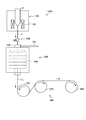
図1は、本発明の実施形態に係る光ファイバ素線の製造方法に用いる光ファイバ素線の製造装置1000の全体構成を示す概略構成図である。図1に示すように、光ファイバ素線の製造装置1000は、線引き炉100と樹脂塗布装置200と紫外線照射装置300と巻き取り装置400とを備えている。
FIG. 1 is a schematic configuration diagram showing an overall configuration of an optical fiber manufacturing apparatus 1000 used in an optical fiber manufacturing method according to an embodiment of the present invention. As shown in FIG. 1, the optical fiber manufacturing apparatus 1000 includes a drawing furnace 100, a resin coating apparatus 200, an ultraviolet irradiation apparatus 300, and a winding apparatus 400.
線引き炉100は、光ファイバ母材Pから光ファイバF1を製造するためのものであり、光ファイバ母材Pを加熱するためのヒータ110を備えている。光ファイバ母材Pは、最終製品においてコアとなる領域の外側にクラッドとなる領域を形成した中間製品である。光ファイバF1は、この光ファイバ母材Pを規格外径(例えば125μm)となるように引き延ばすことによって製造される。
The drawing furnace 100 is for manufacturing the optical fiber F 1 from the optical fiber preform P, and includes a heater 110 for heating the optical fiber preform P. The optical fiber preform P is an intermediate product in which a cladding region is formed outside a core region in the final product. The optical fiber F 1 is manufactured by stretching the optical fiber preform P so as to have a standard outer diameter (for example, 125 μm).
線引き炉100が備えているヒータ110は、光ファイバ母材Pの下端を約2000℃に加熱する。ヒータ110の加熱によって軟化した光ファイバ母材Pの下端は、後段の巻き取り装置400によって引き延ばされる構成である。線引き炉100によって製造される光ファイバF1の外径は、ヒータ110の温度および巻き取り装置400の巻き取り速度等によって調整される。
The heater 110 provided in the drawing furnace 100 heats the lower end of the optical fiber preform P to about 2000 ° C. The lower end of the optical fiber preform P softened by the heating of the heater 110 is configured to be stretched by the subsequent winding device 400. Outer diameter of the optical fiber F 1 produced by drawing furnace 100 is adjusted by the winding speed of the temperature and take-up device 400 of the heater 110.
樹脂塗布装置200および紫外線照射装置300は、それぞれ光ファイバF1の外周に紫外線硬化樹脂を塗布する装置、および、光ファイバF1の外周に塗布された紫外線硬化樹脂を硬化するための装置である。一般に、光ファイバF1の外周には、内側のプライマリ層と外側のセカンダリ層との少なくとも2層の被覆が形成される。そして、光ファイバF1の外周に多層の被覆を形成する方法としては、Wet-on-Wet方式と、Wet-on-Dry方式とが知られている。
Resin coating device 200 and an ultraviolet irradiation apparatus 300, apparatus for applying a UV curing resin on the outer periphery of the optical fiber F 1, respectively, and is the apparatus for curing the applied ultraviolet-curing resin on the outer periphery of the optical fiber F 1 . Generally, the outer periphery of the optical fiber F 1, the coating of at least two layers of the inner primary layer and the outer secondary layer is formed. Then, as a method for forming a multilayer coating on the outer circumference of the optical fiber F 1 is a Wet-on-Wet method, it is known and Wet-on-Dry method.
Wet-on-Wet方式は、樹脂塗布装置200にて複数の紫外線硬化樹脂を光ファイバF1上に塗布し、紫外線照射装置300にて当該複数の紫外線硬化樹脂を一度の紫外線照射によってまとめて硬化させる方法である。
In the wet-on-wet method, a plurality of ultraviolet curable resins are applied onto the optical fiber F 1 by the resin coating apparatus 200, and the plurality of ultraviolet curable resins are collectively cured by one ultraviolet irradiation by the ultraviolet irradiation apparatus 300. It is a method to make.
一方、Wet-on-Dry方式は、樹脂塗布装置200と紫外線照射装置300との組を複数段備え、各段の樹脂塗布装置200と紫外線照射装置300とによって1層毎に被覆を形成する方法である。
On the other hand, the Wet-on-Dry method includes a plurality of sets of a resin coating apparatus 200 and an ultraviolet irradiation apparatus 300, and a coating is formed for each layer by the resin coating apparatus 200 and the ultraviolet irradiation apparatus 300 at each stage. It is.
したがって、図1に示す光ファイバ素線の製造装置1000は、厳密にはWet-on-Wet方式の装置構成となる。しかしながら、本発明の実施形態はWet-on-Wet方式の光ファイバ素線の製造装置1000に限定されるものではない。Wet-on-Dry方式の光ファイバ素線の製造装置1000の場合であっても、複数段の樹脂塗布装置200と紫外線照射装置300との組のうち少なくとも一つ、また、好ましくはすべての組に対して本発明の実施形態を適用することができる。ここでは、単に記載の重複を避けるために、樹脂塗布装置200と紫外線照射装置300とを1組だけ備えた光ファイバ素線の製造装置1000の構成を用いて、本発明の実施形態を説明するものとする。
Therefore, strictly speaking, the optical fiber manufacturing apparatus 1000 shown in FIG. 1 has a wet-on-wet system configuration. However, the embodiment of the present invention is not limited to the wet-on-wet optical fiber manufacturing apparatus 1000. Even in the case of the wet-on-dry optical fiber manufacturing apparatus 1000, at least one of a set of a plurality of stages of the resin coating apparatus 200 and the ultraviolet irradiation apparatus 300, and preferably all sets. The embodiment of the present invention can be applied to the above. Here, in order to avoid duplication of description, an embodiment of the present invention will be described using the configuration of an optical fiber manufacturing apparatus 1000 that includes only one set of a resin coating device 200 and an ultraviolet irradiation device 300. Shall.
図1に示すように、樹脂塗布装置200は、線引き炉100によって製造された光ファイバF1が内部を通過するように構成されている。光ファイバF1は、樹脂塗布装置200の内部を通過する際に、プライマリ層用の紫外線硬化樹脂、および/または、セカンダリ用の紫外線硬化樹脂が塗布される。
As shown in FIG. 1, the resin coating apparatus 200 is configured such that an optical fiber F 1 manufactured by a drawing furnace 100 passes through the inside. Optical fiber F 1, when passing through the interior of the resin coating device 200, an ultraviolet curable resin for the primary layer, and / or an ultraviolet curable resin for the secondary is applied.
紫外線硬化樹脂は、例えば、紫外線で重合・硬化するエチレン性不飽和基を少なくとも2つ有する樹脂であり、好ましくはオリゴマーを使用する。なお、ここでオリゴマーとは、重合度が2~100の重合体である。また、紫外線硬化樹脂には、後に例示する光重合開始剤が添加されている。
The ultraviolet curable resin is, for example, a resin having at least two ethylenically unsaturated groups that are polymerized and cured by ultraviolet rays, and preferably an oligomer. Here, the oligomer is a polymer having a polymerization degree of 2 to 100. Moreover, the photoinitiator illustrated later is added to the ultraviolet curable resin.
さらに、紫外線硬化樹脂は、オリゴマーおよび光重合開始剤に加えて、例えば希釈モノマー、光増感剤、シランカップリング剤、連鎖移動剤および各種添加剤を含んでもよい。希釈モノマーとしては、単官能(メタ)アクリレートまたは多官能(メタ)アクリレートが用いられる。ここで、希釈モノマーとは、紫外線硬化樹脂を希釈するためのモノマーを意味する。
Furthermore, the ultraviolet curable resin may contain, for example, a dilution monomer, a photosensitizer, a silane coupling agent, a chain transfer agent, and various additives in addition to the oligomer and the photopolymerization initiator. As the dilution monomer, monofunctional (meth) acrylate or polyfunctional (meth) acrylate is used. Here, the dilution monomer means a monomer for diluting the ultraviolet curable resin.
半導体紫外線発光素子光源より発せられる発光波長領域が350~405nmである場合、この波長領域に紫外線吸収を有し、組成物を好適に硬化させ得る光重合開始剤として以下のものを用いることができる。
When the emission wavelength region emitted from the light source of the semiconductor ultraviolet light emitting element is 350 to 405 nm, the following can be used as a photopolymerization initiator having ultraviolet absorption in this wavelength region and capable of suitably curing the composition. .
例えば、α―アミノケトン型である、2-メチル-1-[4-(メチルチオ)フェニル]-2-モルホリノプロパノン-1、2-ベンジル-2-ジメチルアミノ-1-(4-モルホリノフェニル)-ブタン-1-オン、2-(ジメチルアミノ)-2-[(4-メチルフェニル)メチル]-1-[4-(4-モルホリニル)フェニル]-1-ブタノン、N,N-ジメチルアミノアセトフェノン等を挙げることができる。市販品では、Irgacure907、Irgacure369およびIrgacure379(商品名、BASFジャパン株式会社製)等を挙げることができる。なお、「Irgacure」は、BASFジャパン株式会社の登録商標である。
For example, α-aminoketone type 2-methyl-1- [4- (methylthio) phenyl] -2-morpholinopropanone-1,2-benzyl-2-dimethylamino-1- (4-morpholinophenyl)- Butan-1-one, 2- (dimethylamino) -2-[(4-methylphenyl) methyl] -1- [4- (4-morpholinyl) phenyl] -1-butanone, N, N-dimethylaminoacetophenone, etc. Can be mentioned. Examples of commercially available products include Irgacure 907, Irgacure 369, and Irgacure 379 (trade name, manufactured by BASF Japan Ltd.). “Irgacure” is a registered trademark of BASF Japan Ltd.
アシルホスフィンオキサイド型である、2,4,6-トリメチルベンゾイルジフェニルホスフィンオキサイド、ビス(2,4,6-トリメチルベンゾイル)-フェニルホスフィンオキサイド、ビス(2,6-ジメトキシベンゾイル)-2,4,4-トリメチル-ペンチルホスフィンオキサイド等を挙げることができる。市販品では、Irgacure819、LucirinTPO、LucirinTPO―LおよびIrgacure2100(商品名、BASFジャパン株式会社製)等を挙げることができる。
2,4,6-trimethylbenzoyldiphenylphosphine oxide, bis (2,4,6-trimethylbenzoyl) -phenylphosphine oxide, bis (2,6-dimethoxybenzoyl) -2,4,4, which are acylphosphine oxide types And -trimethyl-pentylphosphine oxide. Examples of commercially available products include Irgacure 819, Lucirin TPO, Lucirin TPO-L, and Irgacure 2100 (trade name, manufactured by BASF Japan Ltd.).
O-アシルオキシム型である、市販品の、IrgacureOXE01およびIrgacureOXE02(商品名、BASFジャパン株式会社製)を挙げることができる。
Examples include commercially available Irgacure OXE01 and Irgacure OXE02 (trade names, manufactured by BASF Japan Ltd.), which are O-acyloxime types.
図1に示すように、紫外線照射装置300は、樹脂塗布装置200によって紫外線硬化樹脂が塗布された光ファイバF1が内部を通過するように構成されている。光ファイバF1は、紫外線照射装置300の内部を通過する際に紫外線が照射され、塗布された紫外線硬化樹脂が硬化される。
As shown in FIG. 1, the ultraviolet irradiation device 300 is configured such that an optical fiber F 1 coated with an ultraviolet curable resin by the resin coating device 200 passes through the inside. The optical fiber F 1 is irradiated with ultraviolet rays when passing through the ultraviolet irradiation device 300, and the applied ultraviolet curable resin is cured.
紫外線照射装置300は、透明管310と複数の紫外線照射ユニット320と不活性ガス導入管331を備えている。透明管310は、紫外線に対して透光性を有しており、透明管310の中心軸付近を長手方向に光ファイバF1が通過するように構成されている。紫外線照射ユニット320は、透明管310の内部を通過する光ファイバF1に対して紫外線ないし深紫外線を照射する半導体紫外線発光素子を有している。紫外線照射ユニット320および半導体紫外線発光素子の構成は、後に実施例として例示するように、複数種類の構成を採用し得る。
The ultraviolet irradiation device 300 includes a transparent tube 310, a plurality of ultraviolet irradiation units 320, and an inert gas introduction tube 331. The transparent tube 310 is transparent to ultraviolet rays, and is configured such that the optical fiber F 1 passes in the longitudinal direction near the central axis of the transparent tube 310. The ultraviolet irradiation unit 320 includes a semiconductor ultraviolet light emitting element that irradiates the optical fiber F 1 passing through the transparent tube 310 with ultraviolet rays or deep ultraviolet rays. As the configurations of the ultraviolet irradiation unit 320 and the semiconductor ultraviolet light emitting element, a plurality of types of configurations can be adopted as will be exemplified later.
なお、深紫外線は、紫外線の一部であるが、ここでは以下のように定義する。波長365nm~405nmの紫外線を単に紫外線といい、波長200nm~350nmの紫外線を深紫外線という。しかしながら、紫外線照射ユニット320は、複数の紫外線照射ユニットの総括名であるので、紫外線を放射する半導体紫外線発光素子を有するものと深紫外線を放射する半導体紫外線発光素子を有するものとを含む。
In addition, deep ultraviolet rays are a part of ultraviolet rays, but are defined as follows here. Ultraviolet light having a wavelength of 365 nm to 405 nm is simply referred to as ultraviolet light, and ultraviolet light having a wavelength of 200 nm to 350 nm is referred to as deep ultraviolet light. However, since the ultraviolet irradiation unit 320 is a collective name of a plurality of ultraviolet irradiation units, the ultraviolet irradiation unit 320 includes a semiconductor ultraviolet light emitting element that emits ultraviolet light and a semiconductor ultraviolet light emitting element that emits deep ultraviolet light.
不活性ガス導入管331は、透明管310の内部に不活性ガスを充填するためのものである。一般に、紫外線硬化樹脂は、酸素(O2)濃度が高い雰囲気下で硬化させると、酸素と反応して硬化が不十分となりとなる。これを防ぐために、不活性ガス導入管331から透明管310の内部に不活性ガスを供給し、透明管310の内部を酸素濃度が低い雰囲気とする。ここで、不活性ガスは、光ファイバF1およびこれに塗布する紫外線硬化樹脂に対して不活性であれば種類を限定するものではないが、窒素(N2)を用いることが簡便である。
The inert gas introduction pipe 331 is for filling the inside of the transparent pipe 310 with an inert gas. In general, when an ultraviolet curable resin is cured in an atmosphere having a high oxygen (O 2 ) concentration, it reacts with oxygen and becomes insufficiently cured. In order to prevent this, an inert gas is supplied from the inert gas introduction pipe 331 to the inside of the transparent pipe 310 so that the inside of the transparent pipe 310 has an atmosphere having a low oxygen concentration. Here, the type of inert gas is not limited as long as it is inert to the optical fiber F 1 and the ultraviolet curable resin applied to the optical fiber F 1, but it is convenient to use nitrogen (N 2 ).
紫外線照射装置300によって外周に塗布された紫外線硬化樹脂が硬化された光ファイバF1は、光ファイバ素線F2として巻き取り装置400に巻き取られる。巻き取り装置400は、ガイドローラ410,420と巻き取りドラム430とを備えている。なお、図示される巻き取り装置400の例は、1つの構成例であり、ローラの数および配置は変更し得る。先述したように、巻き取り装置400は、光ファイバ素線F2を巻き取る速度を調節することで、線引き炉100で製造される光ファイバF1の外径を制御する。
The optical fiber F 1 in which the ultraviolet curable resin applied to the outer periphery by the ultraviolet irradiation device 300 is cured is wound around the winding device 400 as an optical fiber strand F 2 . The winding device 400 includes guide rollers 410 and 420 and a winding drum 430. The illustrated example of the winding device 400 is one configuration example, and the number and arrangement of rollers can be changed. As described above, the winding device 400 controls the outer diameter of the optical fiber F 1 manufactured in the drawing furnace 100 by adjusting the speed at which the optical fiber F 2 is wound.
以上説明したように、図1に示される光ファイバ素線の製造装置1000は、光ファイバF1の外周に塗布された紫外線硬化樹脂に半導体紫外線発光素子から発せられる紫外線を照射して、紫外線硬化樹脂を硬化させ、光ファイバ素線F2を製造することができる装置である。
As described above, the optical fiber manufacturing apparatus 1000 shown in FIG. 1 irradiates the ultraviolet curable resin applied to the outer periphery of the optical fiber F 1 with ultraviolet rays emitted from the semiconductor ultraviolet light emitting element, thereby curing the ultraviolet rays. This is an apparatus capable of producing the optical fiber F 2 by curing the resin.
以下、紫外線照射装置における紫外線照射ユニットおよび半導体紫外線発光素子の構成の例について説明する。
Hereinafter, examples of configurations of the ultraviolet irradiation unit and the semiconductor ultraviolet light emitting element in the ultraviolet irradiation apparatus will be described.
(実施例1)
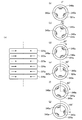
図2は、実施例1に係る紫外線照射ユニットおよび半導体紫外線発光素子の構成を示す図である。なお、実施例1に係る紫外線照射ユニットは、上記説明した紫外線照射装置300における複数の紫外線照射ユニット320として適用し得るものである。したがって、説明の重複を避けるために、図2には、紫外線照射ユニットおよび半導体紫外線発光素子の構成および配置のみを記載し、その他の構成に関しては省略している。 Example 1
FIG. 2 is a diagram illustrating a configuration of the ultraviolet irradiation unit and the semiconductor ultraviolet light emitting element according to the first embodiment. In addition, the ultraviolet irradiation unit which concerns on Example 1 is applicable as the severalultraviolet irradiation unit 320 in the ultraviolet irradiation apparatus 300 demonstrated above. Therefore, in order to avoid duplication of explanation, FIG. 2 shows only the configuration and arrangement of the ultraviolet irradiation unit and the semiconductor ultraviolet light emitting element, and omits other configurations.
図2は、実施例1に係る紫外線照射ユニットおよび半導体紫外線発光素子の構成を示す図である。なお、実施例1に係る紫外線照射ユニットは、上記説明した紫外線照射装置300における複数の紫外線照射ユニット320として適用し得るものである。したがって、説明の重複を避けるために、図2には、紫外線照射ユニットおよび半導体紫外線発光素子の構成および配置のみを記載し、その他の構成に関しては省略している。 Example 1
FIG. 2 is a diagram illustrating a configuration of the ultraviolet irradiation unit and the semiconductor ultraviolet light emitting element according to the first embodiment. In addition, the ultraviolet irradiation unit which concerns on Example 1 is applicable as the several
図2に示すように、実施例1に係る紫外線照射ユニットは、紫外線硬化樹脂に紫外線を照射する第1から第6の紫外線照射ユニット321a~326aによって構成されている。図2(b)~(g)に示すように、第1から第6の紫外線照射ユニット321a~326aは、半導体紫外線発光素子340aを同一円の円周上に3つ配置した同型のユニットであり、図2(a)に示すように、これら第1から第6の紫外線照射ユニット321a~326aは、円の中心を光ファイバが通過するように光ファイバの走行方向に配列されている。
As shown in FIG. 2, the ultraviolet irradiation unit according to the first embodiment includes first to sixth ultraviolet irradiation units 321a to 326a that irradiate ultraviolet curable resin with ultraviolet rays. As shown in FIGS. 2B to 2G, the first to sixth ultraviolet irradiation units 321a to 326a are the same type units in which three semiconductor ultraviolet light emitting elements 340a are arranged on the circumference of the same circle. As shown in FIG. 2A, these first to sixth ultraviolet irradiation units 321a to 326a are arranged in the traveling direction of the optical fiber so that the optical fiber passes through the center of the circle.
なお、図2(a)には光ファイバの記載が省略されているが、紙面の下方向が光ファイバの走行方向に対応し、一点鎖線で記される直線が、光ファイバの走行位置に対応している。また、光ファイバは、半導体紫外線発光素子340aが配置される円の中心を通過するように構成されているので、光ファイバの走行位置は、半導体紫外線発光素子340aの配置位置で規定される円筒面の中心軸に一致している。
In FIG. 2A, the optical fiber is not shown, but the downward direction in the drawing corresponds to the traveling direction of the optical fiber, and the straight line indicated by the alternate long and short dash line corresponds to the traveling position of the optical fiber. is doing. Further, since the optical fiber is configured to pass through the center of the circle where the semiconductor ultraviolet light emitting element 340a is arranged, the traveling position of the optical fiber is a cylindrical surface defined by the arrangement position of the semiconductor ultraviolet light emitting element 340a. Coincides with the central axis.
図2(b)~(g)に示すように、第1から第6の紫外線照射ユニット321a~326aは、光ファイバの走行方向を軸とした円周方向の角度に関して異なる配置となっている。具体的には、第1の紫外線照射ユニット321aの角度を基準として、第2から第6の紫外線照射ユニット322a~326aは、それぞれ、20°,40°,60°,80°,100°で角度が変えられている。
As shown in FIGS. 2B to 2G, the first to sixth ultraviolet irradiation units 321a to 326a are arranged differently with respect to the angle in the circumferential direction with the traveling direction of the optical fiber as an axis. Specifically, with reference to the angle of the first ultraviolet irradiation unit 321a, the second to sixth ultraviolet irradiation units 322a to 326a have angles of 20 °, 40 °, 60 °, 80 °, and 100 °, respectively. Has been changed.
したがって、第1から第6の紫外線照射ユニット321a~326aが備える半導体紫外線発光素子340aは、第1から第6の紫外線照射ユニット321a~326aが光ファイバの走行方向に配列された際に、当該光ファイバの走行方向を軸とした螺旋の上に配置されることになる。また、第1から第6の紫外線照射ユニット321a~326aが備える半導体紫外線発光素子340aは、すべてが光ファイバの走行方向を軸とした円周方向の角度に関して異なる角度となっており、しかもその間隔は円周方向の角度が等しい。結果、光ファイバの円周方向に関して紫外線が均等に照射され、良好な被覆が形成されることになる。
Therefore, the semiconductor ultraviolet light emitting elements 340a included in the first to sixth ultraviolet irradiation units 321a to 326a are arranged so that the first to sixth ultraviolet irradiation units 321a to 326a are arranged in the optical fiber traveling direction. It is arranged on a spiral with the traveling direction of the fiber as an axis. Further, the semiconductor ultraviolet light emitting elements 340a included in the first to sixth ultraviolet irradiation units 321a to 326a are all at different angles with respect to the angle in the circumferential direction with the traveling direction of the optical fiber as an axis, and the interval therebetween. Are equal in circumferential angle. As a result, the ultraviolet rays are uniformly irradiated in the circumferential direction of the optical fiber, and a good coating is formed.
なお、図2(a)に示された第1から第6の紫外線照射ユニット321a~326aに記載された矢印は、半導体紫外線発光素子340aから放射される紫外線の照射方向を示している。つまり、第1から第6の紫外線照射ユニット321a~326aが備える半導体紫外線発光素子340aは、光ファイバの走行方向を示す軸に対して垂直に紫外線を照射している。
It should be noted that the arrows described in the first to sixth ultraviolet irradiation units 321a to 326a shown in FIG. 2A indicate the irradiation direction of the ultraviolet rays emitted from the semiconductor ultraviolet light emitting element 340a. That is, the semiconductor ultraviolet light emitting element 340a included in the first to sixth ultraviolet irradiation units 321a to 326a irradiates ultraviolet rays perpendicular to the axis indicating the traveling direction of the optical fiber.
(実施例2)
図3は、実施例2に係る紫外線照射ユニットおよび半導体紫外線発光素子の構成を示す図である。なお、実施例2に係る紫外線照射ユニットも、上記説明した紫外線照射装置300における複数の紫外線照射ユニット320として適用し得るものである。 (Example 2)
FIG. 3 is a diagram illustrating a configuration of the ultraviolet irradiation unit and the semiconductor ultraviolet light emitting element according to the second embodiment. The ultraviolet irradiation unit according to the second embodiment can also be applied as the plurality ofultraviolet irradiation units 320 in the ultraviolet irradiation apparatus 300 described above.
図3は、実施例2に係る紫外線照射ユニットおよび半導体紫外線発光素子の構成を示す図である。なお、実施例2に係る紫外線照射ユニットも、上記説明した紫外線照射装置300における複数の紫外線照射ユニット320として適用し得るものである。 (Example 2)
FIG. 3 is a diagram illustrating a configuration of the ultraviolet irradiation unit and the semiconductor ultraviolet light emitting element according to the second embodiment. The ultraviolet irradiation unit according to the second embodiment can also be applied as the plurality of
図3に示すように、実施例2に係る紫外線照射ユニットは、紫外線硬化樹脂に紫外線を照射する第1から第4の紫外線照射ユニット321b~324bによって構成されている。図3(b)~(e)に示すように、第1から第4の紫外線照射ユニット321b~324bは、半導体紫外線発光素子340bを同一円の円周上に4つ配置した同型のユニットであり、図3(a)に示すように、これら第1から第4の紫外線照射ユニット321b~324bは、円の中心を光ファイバが通過するように光ファイバの走行方向に配列されている。
As shown in FIG. 3, the ultraviolet irradiation unit according to the second embodiment includes first to fourth ultraviolet irradiation units 321b to 324b that irradiate ultraviolet curable resin with ultraviolet rays. As shown in FIGS. 3B to 3E, the first to fourth ultraviolet irradiation units 321b to 324b are the same type units in which four semiconductor ultraviolet light emitting elements 340b are arranged on the circumference of the same circle. As shown in FIG. 3A, these first to fourth ultraviolet irradiation units 321b to 324b are arranged in the traveling direction of the optical fiber so that the optical fiber passes through the center of the circle.
なお、図3(a)には光ファイバの記載が省略されているが、紙面の下方向が光ファイバの走行方向に対応し、一点鎖線で記される直線が、光ファイバの走行位置に対応している。また、光ファイバは、半導体紫外線発光素子340bが配置される円の中心を通過するように構成されているので、光ファイバの走行位置は、半導体紫外線発光素子340bの配置位置で規定される円筒面の中心軸に一致している。
In FIG. 3A, the description of the optical fiber is omitted, but the downward direction on the paper corresponds to the traveling direction of the optical fiber, and the straight line indicated by the alternate long and short dash line corresponds to the traveling position of the optical fiber. is doing. Further, since the optical fiber is configured to pass through the center of the circle where the semiconductor ultraviolet light emitting element 340b is arranged, the traveling position of the optical fiber is a cylindrical surface defined by the arrangement position of the semiconductor ultraviolet light emitting element 340b. Coincides with the central axis.
図3(b)~(e)に示すように、第1から第4の紫外線照射ユニット321b~324bは、光ファイバの走行方向を軸とした円周方向の角度に関して異なる配置となっている。具体的には、第1の紫外線照射ユニット321bの角度を基準として、第2から第4の紫外線照射ユニット322b~324bは、それぞれ、22.5°,45°,67.5°で角度が変えられている。
As shown in FIGS. 3B to 3E, the first to fourth ultraviolet irradiation units 321b to 324b are arranged differently with respect to the angle in the circumferential direction about the traveling direction of the optical fiber. Specifically, with the angle of the first ultraviolet irradiation unit 321b as a reference, the second to fourth ultraviolet irradiation units 322b to 324b change the angles at 22.5 °, 45 °, and 67.5 °, respectively. It has been.
したがって、第1から第4の紫外線照射ユニット321b~324bが備える半導体紫外線発光素子340bは、第1から第4の紫外線照射ユニット321b~324bが光ファイバの走行方向に配列された際に、当該光ファイバの走行方向を軸とした螺旋の上に配置されることになる。また、第1から第4の紫外線照射ユニット321b~324bが備える半導体紫外線発光素子340bは、すべてが光ファイバの走行方向を軸とした円周方向の角度に関して異なる角度となっており、しかもその間隔は円周方向の角度が等しい。結果、光ファイバの円周方向に関して紫外線が均等に照射され、良好な被覆が形成されることになる。
Therefore, the semiconductor ultraviolet light emitting elements 340b included in the first to fourth ultraviolet irradiation units 321b to 324b are arranged so that the first to fourth ultraviolet irradiation units 321b to 324b are arranged in the traveling direction of the optical fiber. It is arranged on a spiral with the traveling direction of the fiber as an axis. Further, the semiconductor ultraviolet light emitting elements 340b included in the first to fourth ultraviolet irradiation units 321b to 324b are all at different angles with respect to the angle in the circumferential direction with the traveling direction of the optical fiber as an axis. Are equal in circumferential angle. As a result, the ultraviolet rays are uniformly irradiated in the circumferential direction of the optical fiber, and a good coating is formed.
なお、図3(a)に示された第1から第4の紫外線照射ユニット321b~324bに記載された矢印は、半導体紫外線発光素子340bから放射される紫外線の照射方向を示している。つまり、第1から第4の紫外線照射ユニット321b~324bが備える半導体紫外線発光素子340bは、光ファイバの走行方向を示す軸に対して垂直に紫外線を照射している。
It should be noted that the arrows described in the first to fourth ultraviolet irradiation units 321b to 324b shown in FIG. 3A indicate the irradiation direction of the ultraviolet rays emitted from the semiconductor ultraviolet light emitting element 340b. That is, the semiconductor ultraviolet light emitting element 340b included in the first to fourth ultraviolet irradiation units 321b to 324b irradiates ultraviolet rays perpendicular to the axis indicating the traveling direction of the optical fiber.
(実施例3)
図4は、実施例3に係る紫外線照射ユニットおよび半導体紫外線発光素子の構成を示す図である。なお、実施例3に係る紫外線照射ユニットも、上記説明した紫外線照射装置300における複数の紫外線照射ユニット320として適用し得るものである。 (Example 3)
FIG. 4 is a diagram illustrating a configuration of the ultraviolet irradiation unit and the semiconductor ultraviolet light emitting element according to the third embodiment. The ultraviolet irradiation unit according to the third embodiment can also be applied as the plurality ofultraviolet irradiation units 320 in the ultraviolet irradiation apparatus 300 described above.
図4は、実施例3に係る紫外線照射ユニットおよび半導体紫外線発光素子の構成を示す図である。なお、実施例3に係る紫外線照射ユニットも、上記説明した紫外線照射装置300における複数の紫外線照射ユニット320として適用し得るものである。 (Example 3)
FIG. 4 is a diagram illustrating a configuration of the ultraviolet irradiation unit and the semiconductor ultraviolet light emitting element according to the third embodiment. The ultraviolet irradiation unit according to the third embodiment can also be applied as the plurality of
図4に示すように、実施例3に係る紫外線照射ユニットは、紫外線硬化樹脂に紫外線を照射する第1から第5の紫外線照射ユニット321c~325cによって構成されている。図4(b)~(f)に示すように、第1から第5の紫外線照射ユニット321c~325cは、半導体紫外線発光素子340cを同一円の円周上に3つ配置した同型のユニットであり、図4(a)に示すように、これら第1から第5の紫外線照射ユニット321c~325cは、円の中心を光ファイバが通過するように光ファイバの走行方向に配列されている。
As shown in FIG. 4, the ultraviolet irradiation unit according to the third embodiment includes first to fifth ultraviolet irradiation units 321c to 325c that irradiate ultraviolet curable resin with ultraviolet rays. As shown in FIGS. 4B to 4F, the first to fifth ultraviolet irradiation units 321c to 325c are the same type units in which three semiconductor ultraviolet light emitting elements 340c are arranged on the circumference of the same circle. As shown in FIG. 4A, these first to fifth ultraviolet irradiation units 321c to 325c are arranged in the traveling direction of the optical fiber so that the optical fiber passes through the center of the circle.
なお、図4(a)には光ファイバの記載が省略されているが、紙面の下方向が光ファイバの走行方向に対応し、一点鎖線で記される直線が、光ファイバの走行位置に対応している。また、光ファイバは、半導体紫外線発光素子340cが配置される円の中心を通過するように構成されているので、光ファイバの走行位置は、半導体紫外線発光素子340cの配置位置で規定される円筒面の中心軸に一致している。
Although the optical fiber is not shown in FIG. 4A, the downward direction on the paper corresponds to the traveling direction of the optical fiber, and the straight line indicated by the alternate long and short dash line corresponds to the traveling position of the optical fiber. is doing. Further, since the optical fiber is configured to pass through the center of the circle where the semiconductor ultraviolet light emitting element 340c is arranged, the traveling position of the optical fiber is a cylindrical surface defined by the arrangement position of the semiconductor ultraviolet light emitting element 340c. Coincides with the central axis.
図4(b)~(f)に示すように、第1から第5の紫外線照射ユニット321c~325cは、光ファイバの走行方向を軸とした円周方向の角度に関して異なる配置となっている。具体的には、第1の紫外線照射ユニット321cの角度を基準として、第2から第5の紫外線照射ユニット322c~325cは、それぞれ、24°,48°,72°,96°で角度が変えられている。
As shown in FIGS. 4B to 4F, the first to fifth ultraviolet irradiation units 321c to 325c are arranged differently with respect to the angle in the circumferential direction about the traveling direction of the optical fiber. Specifically, with reference to the angle of the first ultraviolet irradiation unit 321c, the angles of the second to fifth ultraviolet irradiation units 322c to 325c can be changed by 24 °, 48 °, 72 °, and 96 °, respectively. ing.
したがって、第1から第5の紫外線照射ユニット321c~325cが備える半導体紫外線発光素子340cは、第1から第5の紫外線照射ユニット321c~325cが光ファイバの走行方向に配列された際に、当該光ファイバの走行方向を軸とした螺旋の上に配置されることになる。また、第1から第5の紫外線照射ユニット321c~325cが備える半導体紫外線発光素子340cは、すべてが光ファイバの走行方向を軸とした円周方向の角度に関して異なる角度となっており、しかもその間隔は円周方向の角度が等しい。結果、光ファイバの円周方向に関して紫外線が均等に照射され、良好な被覆が形成されることになる。
Accordingly, the semiconductor ultraviolet light emitting elements 340c included in the first to fifth ultraviolet irradiation units 321c to 325c are arranged so that the light beams are emitted when the first to fifth ultraviolet irradiation units 321c to 325c are arranged in the traveling direction of the optical fiber. It is arranged on a spiral with the traveling direction of the fiber as an axis. In addition, the semiconductor ultraviolet light emitting elements 340c included in the first to fifth ultraviolet irradiation units 321c to 325c all have different angles with respect to the angle in the circumferential direction with the traveling direction of the optical fiber as an axis, and the interval therebetween. Are equal in circumferential angle. As a result, the ultraviolet rays are uniformly irradiated in the circumferential direction of the optical fiber, and a good coating is formed.
なお、図4(a)に示された第1から第5の紫外線照射ユニット321c~325cに記載された矢印は、半導体紫外線発光素子340cから放射される紫外線の照射方向を示している。つまり、第1から第5の紫外線照射ユニット321c~325cが備える半導体紫外線発光素子340cは、光ファイバの走行方向を示す軸上の一点の近傍に向けて紫外線を照射するように傾けられて前記紫外線照射ユニットに取り付けられている。後に実験例によって詳説するが、このように半導体紫外線発光素子340cを傾けて配置することにより、紫外線硬化樹脂上に照射される紫外線の照度が高まり、紫外線硬化樹脂の硬化が促進されることになる。
It should be noted that the arrows described in the first to fifth ultraviolet irradiation units 321c to 325c shown in FIG. 4A indicate the irradiation direction of the ultraviolet rays emitted from the semiconductor ultraviolet light emitting element 340c. That is, the semiconductor ultraviolet light emitting element 340c included in the first to fifth ultraviolet irradiation units 321c to 325c is tilted so as to irradiate ultraviolet rays toward one point on the axis indicating the traveling direction of the optical fiber, and the ultraviolet rays are emitted. It is attached to the irradiation unit. As will be described in detail later by an experimental example, by arranging the semiconductor ultraviolet light emitting element 340c in an inclined manner as described above, the illuminance of ultraviolet rays irradiated on the ultraviolet curable resin is increased, and the curing of the ultraviolet curable resin is promoted. .
(実施例4)
図5は、実施例4に係る紫外線照射ユニットおよび半導体紫外線発光素子の構成を示す図である。なお、実施例4に係る紫外線照射ユニットも、上記説明した紫外線照射装置300における複数の紫外線照射ユニット320として適用し得るものである。 (Example 4)
FIG. 5 is a diagram illustrating the configuration of the ultraviolet irradiation unit and the semiconductor ultraviolet light emitting element according to the fourth embodiment. In addition, the ultraviolet irradiation unit which concerns on Example 4 is applicable as the someultraviolet irradiation unit 320 in the ultraviolet irradiation apparatus 300 demonstrated above.
図5は、実施例4に係る紫外線照射ユニットおよび半導体紫外線発光素子の構成を示す図である。なお、実施例4に係る紫外線照射ユニットも、上記説明した紫外線照射装置300における複数の紫外線照射ユニット320として適用し得るものである。 (Example 4)
FIG. 5 is a diagram illustrating the configuration of the ultraviolet irradiation unit and the semiconductor ultraviolet light emitting element according to the fourth embodiment. In addition, the ultraviolet irradiation unit which concerns on Example 4 is applicable as the some
図5に示すように、実施例4に係る紫外線照射ユニットは、紫外線硬化樹脂に紫外線を照射する第1から第6の紫外線照射ユニット321d~326dと深紫外線を照射する深紫外線照射ユニット350dとによって構成されている。図5(b)~(g)に示すように、第1から第6の紫外線照射ユニット321d~326dは、半導体紫外線発光素子340dを同一円の円周上に3つ配置した同型のユニットであり、図5(a)に示すように、これら第1から第6の紫外線照射ユニット321d~326dは、円の中心を光ファイバが通過するように光ファイバの走行方向に配列されている。また、深紫外線照射ユニット350dは、第1の紫外線照射ユニット321dよりも前段部(紙面では上方)に配置されている。なお、深紫外線照射ユニット350dは、深紫外線を放射する半導体紫外線発光素子を、例えば第1の紫外線照射ユニット321dと同様に配置して設けられている。
As shown in FIG. 5, the ultraviolet irradiation unit according to the fourth embodiment includes first to sixth ultraviolet irradiation units 321d to 326d that irradiate ultraviolet curable resin with ultraviolet rays and a deep ultraviolet irradiation unit 350d that irradiates deep ultraviolet rays. It is configured. As shown in FIGS. 5B to 5G, the first to sixth ultraviolet irradiation units 321d to 326d are the same type units in which three semiconductor ultraviolet light emitting elements 340d are arranged on the circumference of the same circle. As shown in FIG. 5A, the first to sixth ultraviolet irradiation units 321d to 326d are arranged in the traveling direction of the optical fiber so that the optical fiber passes through the center of the circle. Further, the deep ultraviolet irradiation unit 350d is disposed in a front part (upward in the drawing) than the first ultraviolet irradiation unit 321d. The deep ultraviolet irradiation unit 350d is provided with semiconductor ultraviolet light emitting elements that emit deep ultraviolet rays, for example, in the same manner as the first ultraviolet irradiation unit 321d.
深紫外線(例えば波長200nm~350nm)は、通常の紫外線(例えば波長365nm~405nm)よりも波長が短いので、通常の紫外線が到達する深さよりも浅い層の紫外線硬化樹脂に作用する。したがって、第1の紫外線照射ユニット321dよりも前段部に深紫外線照射ユニット350dを配置することは、表面に近い層の紫外線硬化樹脂を先に硬化させることになる。先述したように、紫外線硬化樹脂は、酸素濃度が高い雰囲気下で硬化させると、酸素と反応して硬化が不十分となるので、不活性ガスを導入して紫外線硬化樹脂が酸素と反応しないようにしている。第1の紫外線照射ユニット321dよりも前段部に深紫外線照射ユニット350dを配置し、より酸素と反応しやすい表面に近い層の紫外線硬化樹脂を先に硬化させることにより、表面品質の向上に寄与する。
Deep ultraviolet rays (for example, wavelengths of 200 nm to 350 nm) have a shorter wavelength than normal ultraviolet rays (for example, wavelengths of 365 nm to 405 nm), and thus act on the ultraviolet curable resin in a layer shallower than the depth at which normal ultraviolet rays reach. Therefore, disposing the deep ultraviolet irradiation unit 350d in the front stage part of the first ultraviolet irradiation unit 321d causes the layer of the ultraviolet curable resin close to the surface to be cured first. As described above, when the ultraviolet curable resin is cured in an atmosphere having a high oxygen concentration, the ultraviolet curable resin reacts with oxygen to be insufficiently cured, so that an inert gas is introduced so that the ultraviolet curable resin does not react with oxygen. I have to. The deep ultraviolet irradiation unit 350d is disposed in the front part of the first ultraviolet irradiation unit 321d, and the ultraviolet curable resin of the layer close to the surface that is more likely to react with oxygen is cured first, thereby contributing to the improvement of the surface quality. .
なお、実施例4に係る紫外線照射ユニットは、実施例1に係る紫外線照射ユニットに対して深紫外線照射ユニット350dを追加したものと考えることができる。したがって、実施例4に係る紫外線照射ユニットは、実施例1に係る紫外線照射ユニットにおける作用および効果をそのまま継承している。
In addition, it can be considered that the ultraviolet irradiation unit according to the fourth embodiment is obtained by adding the deep ultraviolet irradiation unit 350d to the ultraviolet irradiation unit according to the first embodiment. Therefore, the ultraviolet irradiation unit according to the fourth embodiment inherits the functions and effects of the ultraviolet irradiation unit according to the first embodiment as they are.
(実施例5)
図6は、実施例5に係る紫外線照射ユニットおよび半導体紫外線発光素子の構成を示す図である。なお、実施例5に係る紫外線照射ユニットも、上記説明した紫外線照射装置300における複数の紫外線照射ユニット320として適用し得るものである。 (Example 5)
FIG. 6 is a diagram illustrating a configuration of the ultraviolet irradiation unit and the semiconductor ultraviolet light emitting element according to the fifth embodiment. The ultraviolet irradiation unit according to the fifth embodiment can also be applied as the plurality ofultraviolet irradiation units 320 in the ultraviolet irradiation apparatus 300 described above.
図6は、実施例5に係る紫外線照射ユニットおよび半導体紫外線発光素子の構成を示す図である。なお、実施例5に係る紫外線照射ユニットも、上記説明した紫外線照射装置300における複数の紫外線照射ユニット320として適用し得るものである。 (Example 5)
FIG. 6 is a diagram illustrating a configuration of the ultraviolet irradiation unit and the semiconductor ultraviolet light emitting element according to the fifth embodiment. The ultraviolet irradiation unit according to the fifth embodiment can also be applied as the plurality of
図6に示すように、実施例5に係る紫外線照射ユニットは、紫外線硬化樹脂に紫外線を照射する第1から第4の紫外線照射ユニット321e~324eと深紫外線を照射する深紫外線照射ユニット350eとによって構成されている。図6(b)~(e)に示すように、第1から第4の紫外線照射ユニット321e~324eは、半導体紫外線発光素子340eを同一円の円周上に4つ配置した同型のユニットであり、図6(a)に示すように、これら第1から第4の紫外線照射ユニット321e~324eは、円の中心を光ファイバが通過するように光ファイバの走行方向に配列されている。また、深紫外線照射ユニット350eは、第1の紫外線照射ユニット321eよりも前段部(紙面では上方)に配置されている。なお、深紫外線照射ユニット350eは、実施例4における深紫外線照射ユニット350dと同一の構成を有する。
As shown in FIG. 6, the ultraviolet irradiation unit according to the fifth embodiment includes first to fourth ultraviolet irradiation units 321e to 324e that irradiate ultraviolet curable resin with ultraviolet rays and a deep ultraviolet irradiation unit 350e that irradiates deep ultraviolet rays. It is configured. As shown in FIGS. 6B to 6E, the first to fourth ultraviolet irradiation units 321e to 324e are the same type units in which four semiconductor ultraviolet light emitting elements 340e are arranged on the circumference of the same circle. As shown in FIG. 6A, the first to fourth ultraviolet irradiation units 321e to 324e are arranged in the traveling direction of the optical fiber so that the optical fiber passes through the center of the circle. Further, the deep ultraviolet irradiation unit 350e is arranged in a front stage (upward in the drawing) than the first ultraviolet irradiation unit 321e. The deep ultraviolet irradiation unit 350e has the same configuration as the deep ultraviolet irradiation unit 350d in the fourth embodiment.
実施例4と同様に、第1の紫外線照射ユニット321eよりも前段部に深紫外線照射ユニット350eを配置することは、より酸素と反応しやすい表面に近い層の紫外線硬化樹脂を先に硬化させることにより、表面品質の向上に寄与する。
Similar to the fourth embodiment, disposing the deep ultraviolet irradiation unit 350e in the front stage portion of the first ultraviolet irradiation unit 321e cures the ultraviolet curable resin in a layer close to the surface that is more likely to react with oxygen first. This contributes to improving the surface quality.
なお、実施例5に係る紫外線照射ユニットは、実施例2に係る紫外線照射ユニットに対して深紫外線照射ユニット350eを追加したものと考えることができる。したがって、実施例5に係る紫外線照射ユニットは、実施例2に係る紫外線照射ユニットにおける作用および効果をそのまま継承している。
In addition, it can be considered that the ultraviolet irradiation unit according to the fifth embodiment is obtained by adding the deep ultraviolet irradiation unit 350e to the ultraviolet irradiation unit according to the second embodiment. Therefore, the ultraviolet irradiation unit according to the fifth embodiment inherits the functions and effects of the ultraviolet irradiation unit according to the second embodiment as they are.
(実施例6)
図7は、実施例6に係る紫外線照射ユニットおよび半導体紫外線発光素子の構成を示す図である。なお、実施例6に係る紫外線照射ユニットも、上記説明した紫外線照射装置300における複数の紫外線照射ユニット320として適用し得るものである。 (Example 6)
FIG. 7 is a diagram illustrating a configuration of the ultraviolet irradiation unit and the semiconductor ultraviolet light emitting element according to the sixth embodiment. The ultraviolet irradiation unit according to the sixth embodiment can also be applied as the plurality ofultraviolet irradiation units 320 in the ultraviolet irradiation apparatus 300 described above.
図7は、実施例6に係る紫外線照射ユニットおよび半導体紫外線発光素子の構成を示す図である。なお、実施例6に係る紫外線照射ユニットも、上記説明した紫外線照射装置300における複数の紫外線照射ユニット320として適用し得るものである。 (Example 6)
FIG. 7 is a diagram illustrating a configuration of the ultraviolet irradiation unit and the semiconductor ultraviolet light emitting element according to the sixth embodiment. The ultraviolet irradiation unit according to the sixth embodiment can also be applied as the plurality of
図7に示すように、実施例6に係る紫外線照射ユニットは、紫外線硬化樹脂に紫外線を照射する第1から第5の紫外線照射ユニット321f~325fと深紫外線を照射する深紫外線照射ユニット350fとによって構成されている。図7(b)~(f)に示すように、第1から第5の紫外線照射ユニット321f~325fは、半導体紫外線発光素子340fを同一円の円周上に3つ配置した同型のユニットであり、図7(a)に示すように、これら第1から第5の紫外線照射ユニット321f~325fは、円の中心を光ファイバが通過するように光ファイバの走行方向に配列されている。また、深紫外線照射ユニット350fは、第1の紫外線照射ユニット321fよりも前段部(紙面では上方)に配置されている。なお、深紫外線照射ユニット350fは、実施例4における深紫外線照射ユニット350dと同一の構成を有する。
As shown in FIG. 7, the ultraviolet irradiation unit according to the sixth embodiment includes first to fifth ultraviolet irradiation units 321f to 325f for irradiating ultraviolet curable resin with ultraviolet rays and a deep ultraviolet irradiation unit 350f for irradiating deep ultraviolet rays. It is configured. As shown in FIGS. 7B to 7F, the first to fifth ultraviolet irradiation units 321f to 325f are the same type units in which three semiconductor ultraviolet light emitting elements 340f are arranged on the circumference of the same circle. As shown in FIG. 7A, the first to fifth ultraviolet irradiation units 321f to 325f are arranged in the traveling direction of the optical fiber so that the optical fiber passes through the center of the circle. Further, the deep ultraviolet irradiation unit 350f is disposed in a front part (upward in the drawing) than the first ultraviolet irradiation unit 321f. The deep ultraviolet irradiation unit 350f has the same configuration as the deep ultraviolet irradiation unit 350d in the fourth embodiment.
実施例4と同様に、第1の紫外線照射ユニット321fよりも前段部に深紫外線照射ユニット350fを配置することは、より酸素と反応しやすい表面に近い層の紫外線硬化樹脂を先に硬化させることにより、表面品質の向上に寄与する。
As in the fourth embodiment, disposing the deep ultraviolet irradiation unit 350f in front of the first ultraviolet irradiation unit 321f allows the ultraviolet curing resin of the layer closer to the surface that is more likely to react with oxygen to be cured first. This contributes to improving the surface quality.
なお、実施例6に係る紫外線照射ユニットは、実施例3に係る紫外線照射ユニットに対して深紫外線照射ユニット350fを追加したものと考えることができる。したがって、実施例6に係る紫外線照射ユニットは、実施例3に係る紫外線照射ユニットにおける作用および効果をそのまま継承している。
It can be considered that the ultraviolet irradiation unit according to the sixth embodiment is obtained by adding the deep ultraviolet irradiation unit 350f to the ultraviolet irradiation unit according to the third embodiment. Therefore, the ultraviolet irradiation unit according to the sixth embodiment inherits the functions and effects of the ultraviolet irradiation unit according to the third embodiment as they are.
(比較例)
図8は、比較例に係る紫外線照射ユニットおよび半導体紫外線発光素子の構成を示す図である。当該比較例は、後に説明する本発明の効果を示す検証実験に用いたものである。なお、比較例に係る紫外線照射ユニットも、上記説明した紫外線照射装置300における複数の紫外線照射ユニット320として適用し得る。 (Comparative example)
FIG. 8 is a diagram showing a configuration of an ultraviolet irradiation unit and a semiconductor ultraviolet light emitting element according to a comparative example. The comparative example is used in a verification experiment showing the effect of the present invention described later. In addition, the ultraviolet irradiation unit which concerns on a comparative example can also be applied as the severalultraviolet irradiation unit 320 in the ultraviolet irradiation apparatus 300 demonstrated above.
図8は、比較例に係る紫外線照射ユニットおよび半導体紫外線発光素子の構成を示す図である。当該比較例は、後に説明する本発明の効果を示す検証実験に用いたものである。なお、比較例に係る紫外線照射ユニットも、上記説明した紫外線照射装置300における複数の紫外線照射ユニット320として適用し得る。 (Comparative example)
FIG. 8 is a diagram showing a configuration of an ultraviolet irradiation unit and a semiconductor ultraviolet light emitting element according to a comparative example. The comparative example is used in a verification experiment showing the effect of the present invention described later. In addition, the ultraviolet irradiation unit which concerns on a comparative example can also be applied as the several
図8に示すように、比較例に係る紫外線照射ユニットは、紫外線硬化樹脂に紫外線を照射する第1から第6の紫外線照射ユニット321g~326gによって構成されている。図8(b)~(g)に示すように、第1から第6の紫外線照射ユニット321g~326gは、半導体紫外線発光素子340gを同一円の円周上に3つ配置した同型のユニットであり、図8(a)に示すように、これら第1から第6の紫外線照射ユニット321g~326gは、円の中心を光ファイバが通過するように光ファイバの走行方向に配列されている。
As shown in FIG. 8, the ultraviolet irradiation unit according to the comparative example is composed of first to sixth ultraviolet irradiation units 321g to 326g that irradiate the ultraviolet curable resin with ultraviolet rays. As shown in FIGS. 8B to 8G, the first to sixth ultraviolet irradiation units 321g to 326g are the same type units in which three semiconductor ultraviolet light emitting elements 340g are arranged on the circumference of the same circle. As shown in FIG. 8A, the first to sixth ultraviolet irradiation units 321g to 326g are arranged in the traveling direction of the optical fiber so that the optical fiber passes through the center of the circle.
したがって、比較例に係る紫外線照射ユニットおよび半導体紫外線発光素子の構成は、実施例1に係る紫外線照射ユニットおよび半導体紫外線発光素子の構成とほぼ同じであるが、比較例では、図8(b)~(g)に示すように、第1から第6の紫外線照射ユニット321g~326gは、光ファイバの走行方向を軸とした円周方向の角度に関して同じ配置となっている。なお、第1から第6の紫外線照射ユニット321g~326gが備える半導体紫外線発光素子340gは、光ファイバの走行方向を示す軸に対して垂直に紫外線を照射している。
Therefore, the configurations of the ultraviolet irradiation unit and the semiconductor ultraviolet light emitting element according to the comparative example are substantially the same as the configurations of the ultraviolet irradiation unit and the semiconductor ultraviolet light emitting element according to the first embodiment, but in the comparative example, FIG. As shown in (g), the first to sixth ultraviolet irradiation units 321g to 326g have the same arrangement with respect to the angle in the circumferential direction about the traveling direction of the optical fiber. The semiconductor ultraviolet light emitting element 340g included in the first to sixth ultraviolet irradiation units 321g to 326g irradiates ultraviolet rays perpendicular to the axis indicating the traveling direction of the optical fiber.
(変形例)
実施例1~6に記載された紫外線照射ユニットまたは深紫外線照射ユニットでは、当該ユニット自体に半導体紫外線発光素子が配置されている。しかしながら、紫外線硬化樹脂に向けて紫外線を照射する位置に、紫外線光源から発せられた紫外線を光ファイバ等で導いて照射する構成を設けてもよい。このような紫外線照射ユニットを実施例1~6と同様に複数配置して、紫外線照射装置を構成すれば、実施例1~6と同様の効果を奏することができる。 (Modification)
In the ultraviolet irradiation unit or deep ultraviolet irradiation unit described in Examples 1 to 6, a semiconductor ultraviolet light emitting element is disposed in the unit itself. However, a configuration in which ultraviolet rays emitted from an ultraviolet light source are guided by an optical fiber or the like may be provided at a position where the ultraviolet rays are irradiated toward the ultraviolet curable resin. By arranging a plurality of such ultraviolet irradiation units in the same manner as in the first to sixth embodiments to form an ultraviolet irradiation device, the same effects as in the first to sixth embodiments can be obtained.
(検証実験)
以下に掲げる表1は、本発明の実施形態に係る光ファイバ素線の製造方法および紫外線照射装置の効果を検証する実験の結果を示す表である。表1に記載の検証実験は、実施例1~6および比較例に記載の構成を適用した紫外線照射装置を用いて光ファイバ素線の製造をした場合の光ファイバ素線の特性を検証したものである。 (Verification experiment)
Table 1 listed below is a table showing results of experiments for verifying the effects of the method for manufacturing an optical fiber and the ultraviolet irradiation device according to the embodiment of the present invention. The verification experiment described in Table 1 verified the characteristics of the optical fiber when the optical fiber was manufactured using the ultraviolet irradiation apparatus to which the configurations described in Examples 1 to 6 and the comparative example were applied. It is.
なお、光ファイバの外周に被覆を形成する方法としては、Wet-on-Dry方式を採用し、効果の検証を容易にするために、セカンダリ層のみに本発明の実施形態を適用している。また、セカンダリ層の紫外線硬化樹脂に用いた光重合開始剤はIrgacure184(BASFジャパン株式会社)である。
As a method for forming the coating on the outer periphery of the optical fiber, a wet-on-dry method is adopted, and the embodiment of the present invention is applied only to the secondary layer in order to easily verify the effect. Moreover, the photoinitiator used for the ultraviolet curable resin of the secondary layer is Irgacure 184 (BASF Japan Ltd.).

表1に記載のように、検証実験では、消費電力の削減率とうねりの有無とknot testとケーブルロスと2.5%モジュラスとを比較している。ここで、消費電力の削減率は、比較例と比べた場合の消費電力の削減率を意味している。うねりの有無の判定は、製造された光ファイバ素線の長さを、張力を掛けた状態と掛けない状態とで測定し、張力を掛けた状態で測定した光ファイバ素線の長さが30mである場合に、張力を掛けない状態で測定した光ファイバ素線の長さが5cm以上縮んでいる場合、うねり有りと判定している。また、張力を掛けた状態とは、ボビンから光ファイバ素線を繰り出す際の張力であり、50gを用いている。
As shown in Table 1, in the verification experiment, the reduction rate of power consumption, the presence or absence of waviness, knot test, cable loss, and 2.5% modulus are compared. Here, the reduction rate of power consumption means the reduction rate of power consumption when compared with the comparative example. The determination of the presence or absence of waviness is made by measuring the length of the manufactured optical fiber in a state where tension is applied and in a state where it is not applied, and the length of the optical fiber measured in the state where tension is applied is 30 m. When the length of the optical fiber measured in a state where no tension is applied is contracted by 5 cm or more, it is determined that there is undulation. The state where tension is applied is the tension when the optical fiber is drawn out from the bobbin, and 50 g is used.
knot testは、光ファイバ素線の表面の動摩擦力の評価である。図9は、実施したknot testの概要を示す模式図である。その測定方法は、図9に示すように、製造した光ファイバ素線F3で一重のループを作り、該ループに光ファイバ素線F3を順次くぐらせて、点A~Eの5箇所で自己と接触する直径約7cmの円を作り、この光ファイバの両端を引張試験機により5mm/分の速度で引っ張る。このときの荷重(N)を計測したものを用いている。
knot test is an evaluation of the dynamic frictional force of the surface of the optical fiber. FIG. 9 is a schematic diagram showing an outline of the performed knot test. As shown in FIG. 9, a single loop is formed with the manufactured optical fiber F 3 , and the optical fiber F 3 is sequentially passed through the loop as shown in FIG. A circle having a diameter of about 7 cm that makes contact with itself is made, and both ends of the optical fiber are pulled at a speed of 5 mm / min by a tensile tester. What measured the load (N) at this time is used.
また、ケーブルロスは、光ファイバ素線を用いて作成したルースチューブ型光ファイバケーブルにおける波長1.55μmの光の伝送に関する損失であり、0.230dB/km以下を許容範囲としている。図10は、ルースチューブ型光ファイバケーブルの構造を示す断面図であり、ケーブルロスの測定は当該ルースチューブ型光ファイバケーブルを用いて測定した。図10に示すようにルースチューブ型光ファイバケーブルF4は、テンションメンバ41、光ファイバ着色心線42、ルースチューブ43、ジェリー44、およびシース45から構成される。テンションメンバ41は、金属またはプラスチックからなる。テンションメンバ41の円柱側面に、金属またはプラスチックからなるルースチューブ43が光ファイバ着色心線42を挿通して複数設けられている。これらのルースチューブ43同士がプラスチックからなるシース45によって覆われ、それらの間隙がジェリー44により埋められている。
The cable loss is a loss related to the transmission of light having a wavelength of 1.55 μm in a loose tube type optical fiber cable created using an optical fiber, and the allowable range is 0.230 dB / km or less. FIG. 10 is a cross-sectional view showing the structure of a loose tube type optical fiber cable, and the cable loss was measured using the loose tube type optical fiber cable. As shown in FIG. 10, the loose tube type optical fiber cable F 4 includes a tension member 41, an optical fiber colored core wire 42, a loose tube 43, a jelly 44, and a sheath 45. The tension member 41 is made of metal or plastic. A plurality of loose tubes 43 made of metal or plastic are provided on the side surface of the tension member 41 through the optical fiber colored core wire 42. These loose tubes 43 are covered with a sheath 45 made of plastic, and a gap between them is filled with a jelly 44.
2.5%モジュラス(弾性率)の値は、以下のようにして測定した。まず、実施例1~6および比較例の構成を適用した紫外線照射装置を用いた製造方法で製造した光ファイバ素線を液体窒素に浸漬し、液体窒素温度で被覆除去冶具を用いてガラス心線を抜き取り、被覆層をチューブ状にする。そして、このチューブ状の光ファイバ被覆層50mm長をサンプルとし、このサンプルをJIS K 7161に準拠して標線間距離25mmで2.5%モジュラスを測定した。
The value of 2.5% modulus (elastic modulus) was measured as follows. First, an optical fiber manufactured by a manufacturing method using an ultraviolet irradiation device to which the configurations of Examples 1 to 6 and the comparative example are applied is immersed in liquid nitrogen, and a glass core wire is used using a coating removal jig at the liquid nitrogen temperature. And the coating layer is formed into a tube shape. And this tube-shaped optical fiber coating layer 50mm length was made into the sample, and 2.5% modulus was measured by 25 mm of distances between marked lines based on this sample based on JISK7161.
表1を見ると解るように、実施例1~6の構成を適用した紫外線照射装置を用いて製造した光ファイバ素線は、うねりが発生しないが、比較例の構成を適用した紫外線照射装置を用いて製造した光ファイバ素線は、うねりが発生している。これは、実施例1~6の構成を適用した紫外線照射装置では、光ファイバの円周方向に関して紫外線が均等に照射され、良好な被覆が形成されたことを示している。
As can be seen from Table 1, the optical fiber manufactured using the ultraviolet irradiation apparatus to which the configurations of Examples 1 to 6 are applied does not generate undulation, but the ultraviolet irradiation apparatus to which the configuration of the comparative example is applied. Waves are generated in the optical fiber produced by using the optical fiber. This indicates that in the ultraviolet irradiation apparatus to which the configurations of Examples 1 to 6 are applied, the ultraviolet rays are uniformly irradiated in the circumferential direction of the optical fiber, and a good coating is formed.
また、表1を見ると解るように、実施例4~6の構成を適用した紫外線照射装置を用いて製造した光ファイバ素線は、knot testの測定結果が著しく改善している。実施例4~6の構成を適用した紫外線照射装置では、深紫外線照射ユニットを用いて表面に近い層の紫外線硬化樹脂を先に硬化させること被覆の表面品質が向上したことを示している。
Also, as can be seen from Table 1, the measurement result of knot test is remarkably improved in the optical fiber manufactured using the ultraviolet irradiation apparatus to which the configurations of Examples 4 to 6 are applied. In the ultraviolet irradiation apparatus to which the configurations of Examples 4 to 6 are applied, it is shown that the surface quality of the coating is improved by first curing the ultraviolet curable resin of the layer close to the surface using the deep ultraviolet irradiation unit.
また、表1を見ると解るように、実施例1~6の構成を適用した紫外線照射装置を用いて製造した光ファイバ素線は、ケーブルロスの値も良好である。
As can be seen from Table 1, the optical fiber manufactured using the ultraviolet irradiation apparatus to which the configurations of Examples 1 to 6 are applied has a good cable loss value.
また、表1を見ると解るように、実施例1~6の構成を適用した紫外線照射装置を用いて製造した光ファイバ素線は、比較例の構成を適用した紫外線照射装置を用いて製造した光ファイバ素線と比較して、2.5%モジュラスが高い。これは、実施例1~6の構成を適用した紫外線照射装置では、紫外線硬化樹脂に対して紫外線が十分に照射され、良好な被覆が形成されたことを示している。
As can be seen from Table 1, the optical fiber manufactured using the ultraviolet irradiation apparatus to which the configurations of Examples 1 to 6 are applied is manufactured using the ultraviolet irradiation apparatus to which the configuration of the comparative example is applied. Compared with an optical fiber, 2.5% modulus is high. This indicates that in the ultraviolet irradiation apparatus to which the configurations of Examples 1 to 6 were applied, the ultraviolet curable resin was sufficiently irradiated with ultraviolet rays and a good coating was formed.
一方で、表1を見ると解るように、実施例2,3,5,6の構成を適用した紫外線照射装置の消費電力は、比較例の構成を適用した紫外線照射装置よりも少ない。これは、実施例2,3,5,6の構成を適用した紫外線照射装置は、比較例の構成を適用した紫外線照射装置よりも、半導体紫外線発光素子の使用個数が少ないからである。なお、実施例5,6の構成を適用した紫外線照射装置では、深紫外線の半導体紫外線発光素子も使用しているが、深紫外線の半導体紫外線発光素子は、通常の半導体紫外線発光素子と比較して消費電力が小さいので、その影響は無視できる程度に少ない。
On the other hand, as can be seen from Table 1, the power consumption of the ultraviolet irradiation device to which the configurations of Examples 2, 3, 5, and 6 are applied is less than that of the ultraviolet irradiation device to which the configuration of the comparative example is applied. This is because the number of semiconductor ultraviolet light emitting elements used is smaller in the ultraviolet irradiation device to which the configurations of Examples 2, 3, 5, and 6 are applied than in the ultraviolet irradiation device to which the configuration of the comparative example is applied. In addition, in the ultraviolet irradiation apparatus to which the configurations of Examples 5 and 6 are applied, a deep ultraviolet semiconductor ultraviolet light emitting element is also used, but the deep ultraviolet semiconductor ultraviolet light emitting element is compared with a normal semiconductor ultraviolet light emitting element. Since power consumption is small, the effect is negligibly small.
上記結果は、実施例2,3,5,6の構成を適用した紫外線照射装置は、うねりの有無、knot test、およびケーブルロス等の性能を維持しながら、紫外線照射装置における消費電力を削減することができることを意味する。
The above results show that the ultraviolet irradiation device to which the configurations of Examples 2, 3, 5, and 6 are applied reduces the power consumption in the ultraviolet irradiation device while maintaining the performance of presence / absence of undulation, knot test, cable loss, and the like. Means that you can.
ここで、実施例3,6の構成の利点に関する検証実験の結果について説明する。実施例3,6の構成では、半導体紫外線発光素子が光ファイバの走行方向を示す軸上の一点の近傍に向けて紫外線を照射するように配置されている。この構成が被覆の硬化にどのように寄与するのかを説明する。
Here, the result of the verification experiment regarding the advantages of the configurations of Examples 3 and 6 will be described. In the configurations of Examples 3 and 6, the semiconductor ultraviolet light emitting element is arranged so as to irradiate ultraviolet rays toward one point on the axis indicating the traveling direction of the optical fiber. It will be described how this configuration contributes to the curing of the coating.
図11は、紫外線硬化樹脂に照射される紫外線の照度(I)と2.5%モジュラス(G)との関係を示すグラフを示す図である。図11に示される測定結果は、以下のような測定によって得られている。
FIG. 11 is a graph showing the relationship between the illuminance (I) of the ultraviolet rays irradiated to the ultraviolet curable resin and the 2.5% modulus (G). The measurement result shown in FIG. 11 is obtained by the following measurement.
石英ガラスからなる基材を用意し、セカンダリ用紫外線硬化樹脂を厚さ50μmでスピンコートする。ここで、セカンダリ用紫外線硬化樹脂は、上記説明した実施例の比較実験で用いた樹脂と同じものである。そして、セカンダリ用紫外線硬化樹脂を塗布した基材をパージボックスに入れ窒素雰囲気にし、コンベヤ型紫外線照射装置にて所定の積算光量になるように照度、速度を調整し、紫外線(365nm)を照射し、樹脂を硬化する。
A base material made of quartz glass is prepared, and a secondary UV curable resin is spin-coated at a thickness of 50 μm. Here, the ultraviolet curable resin for secondary is the same as the resin used in the comparative experiment of the above-described embodiment. Then, the substrate coated with the secondary UV curable resin is placed in a purge box to create a nitrogen atmosphere, and the illuminance and speed are adjusted with a conveyor type UV irradiation device so as to obtain a predetermined integrated light amount, and UV (365 nm) is irradiated. , Cure the resin.
硬化したセカンダリ用紫外線硬化樹脂を基材から剥し、6mm幅の短冊状に切断して50mm以上の長さのサンプルとする。このサンプルをJIS K 7161に準拠して標線間距離25mmで2.5%モジュラス(弾性率)を測定する。
The cured secondary UV curable resin is peeled off from the base material and cut into a strip of 6 mm width to obtain a sample having a length of 50 mm or more. This sample is measured for 2.5% modulus (elastic modulus) in accordance with JIS K 7161 with a distance between marked lines of 25 mm.
図11に示されるグラフから読み取れるように、紫外線硬化樹脂に照射される紫外線の照度が高い方が2.5%モジュラスは高い。したがって、紫外線照射装置において、紫外線硬化樹脂に照射される紫外線の照度が高まる構成を採用した方がより良好な被覆を形成することができる。実施例3,6に係る紫外線照射装置の構成では、半導体紫外線発光素子が光ファイバの走行方向を示す軸上の一点の近傍に向けて紫外線を照射するように構成されているので、紫外線硬化樹脂に照射される紫外線の照度が高まり、より良好な被覆を形成することができるようになっている。
As can be seen from the graph shown in FIG. 11, the higher the illuminance of ultraviolet rays irradiated to the ultraviolet curable resin, the higher the 2.5% modulus. Therefore, in the ultraviolet irradiation device, it is possible to form a better coating by adopting a configuration in which the illuminance of ultraviolet rays irradiated to the ultraviolet curable resin is increased. In the configuration of the ultraviolet irradiation device according to Examples 3 and 6, the semiconductor ultraviolet light emitting element is configured to irradiate ultraviolet rays toward one point on the axis indicating the traveling direction of the optical fiber. The illuminance of the ultraviolet rays irradiated to the surface is increased, so that a better coating can be formed.
以上、本発明の実施形態について具体的に説明したが、本発明は、上述の実施形態に限定されるものではなく、本発明の技術的思想に基づく各種の変形が可能である。例えば、上記説明した実施例1~6では、紫外線照射ユニットのすべてが光ファイバの走行方向を軸とした円周方向の角度に関して異なる配置となっているが、紫外線照射ユニットのうち少なくとも2つが光ファイバの走行方向を軸とした円周方向の角度に関して異なる配置となっているならば、比較例よりも良好な被覆を形成することができる。
The embodiments of the present invention have been specifically described above, but the present invention is not limited to the above-described embodiments, and various modifications based on the technical idea of the present invention are possible. For example, in Examples 1 to 6 described above, all of the ultraviolet irradiation units are arranged differently with respect to the angle in the circumferential direction with the traveling direction of the optical fiber as an axis, but at least two of the ultraviolet irradiation units are light beams. If the arrangement is different with respect to the angle in the circumferential direction about the traveling direction of the fiber, a coating better than that of the comparative example can be formed.
また、上記説明した実施例1~6では、紫外線照射ユニットが備える半導体紫外線発光素子が光ファイバの走行方向を軸とした螺旋の上に配置されているが、必ずしも螺旋配置とする必要はなく、非法則的に半導体紫外線発光素子を光ファイバの走行方向を軸とした円周方向の角度に関して異なるように配置することも可能である。
Further, in Examples 1 to 6 described above, the semiconductor ultraviolet light emitting element provided in the ultraviolet irradiation unit is disposed on a spiral with the traveling direction of the optical fiber as an axis, but it is not always necessary to have a spiral arrangement. It is also possible to arrange the semiconductor ultraviolet light emitting elements differently with respect to the angle in the circumferential direction about the traveling direction of the optical fiber.
また、上記説明した実施例1~6の比較実験では、セカンダリ層のみに着目した比較実験を行ったが、本発明の実施形態をプライマリ層にも適用することが可能である。
Further, in the comparative experiments of Examples 1 to 6 described above, a comparative experiment focusing only on the secondary layer was performed, but the embodiment of the present invention can also be applied to the primary layer.
以上のように、本発明に係る光ファイバ素線の製造方法および紫外線照射装置は、光ファイバ素線の製造に有用である。
As described above, the method for manufacturing an optical fiber and the ultraviolet irradiation device according to the present invention are useful for manufacturing an optical fiber.
1000 光ファイバ素線の製造装置
100 線引き炉
110 ヒータ
200 樹脂塗布装置
300 紫外線照射装置
310 透明管
320,321~326 紫外線照射ユニット
331 不活性ガス導入管
340 半導体紫外線発光素子
350 深紫外線照射ユニット
400 巻き取り装置
410,420 ガイドローラ
430 巻き取りドラム
41 テンションメンバ
42 光ファイバ着色心線
43 ルースチューブ
44 ジェリー
45 シース DESCRIPTION OFSYMBOLS 1000 Optical fiber manufacturing apparatus 100 Drawing furnace 110 Heater 200 Resin coating apparatus 300 Ultraviolet irradiation apparatus 310 Transparent tube 320,321-326 Ultraviolet irradiation unit 331 Inert gas introduction pipe 340 Semiconductor ultraviolet light emitting element 350 Deep ultraviolet irradiation unit 400 Winding Take-up device 410, 420 Guide roller 430 Take-up drum 41 Tension member 42 Optical fiber colored core wire 43 Loose tube 44 Jelly 45 Sheath
100 線引き炉
110 ヒータ
200 樹脂塗布装置
300 紫外線照射装置
310 透明管
320,321~326 紫外線照射ユニット
331 不活性ガス導入管
340 半導体紫外線発光素子
350 深紫外線照射ユニット
400 巻き取り装置
410,420 ガイドローラ
430 巻き取りドラム
41 テンションメンバ
42 光ファイバ着色心線
43 ルースチューブ
44 ジェリー
45 シース DESCRIPTION OF
Claims (12)
- 光ファイバの外周に塗布された紫外線硬化樹脂に半導体紫外線発光素子から発せられる紫外線を照射して、前記紫外線硬化樹脂を硬化させる光ファイバ素線の製造方法であって、
前記紫外線硬化樹脂に向けて前記紫外線を照射する位置が同一円の円周上に複数配置された紫外線照射ユニットが、前記円の中心を前記光ファイバが通過するように前記光ファイバの走行方向に複数配列され、かつ、前記複数の紫外線照射ユニットのうち少なくとも2つが、前記光ファイバの走行方向を軸とした円周方向の角度に関して異なる配置となっている紫外線照射装置を用いて、
前記光ファイバの外周に塗布された紫外線硬化樹脂に紫外線を照射する、
ことを特徴とする光ファイバ素線の製造方法。 A method of manufacturing an optical fiber, wherein the ultraviolet curable resin applied to the outer periphery of the optical fiber is irradiated with ultraviolet rays emitted from a semiconductor ultraviolet light emitting element to cure the ultraviolet curable resin,
A plurality of ultraviolet irradiation units in which the ultraviolet irradiation positions toward the ultraviolet curable resin are arranged on the circumference of the same circle, so that the optical fiber passes through the center of the circle in the traveling direction of the optical fiber. A plurality of ultraviolet irradiation units, and at least two of the plurality of ultraviolet irradiation units are arranged differently with respect to an angle in a circumferential direction around the traveling direction of the optical fiber,
Irradiating the ultraviolet curable resin applied to the outer periphery of the optical fiber with ultraviolet rays;
An optical fiber manufacturing method characterized by that. - 前記紫外線照射ユニットにおける前記位置に、前記半導体紫外線発光素子が配置されている、ことを特徴とする請求項1に記載の光ファイバ素線の製造方法。 The method of manufacturing an optical fiber according to claim 1, wherein the semiconductor ultraviolet light emitting element is disposed at the position in the ultraviolet irradiation unit.
- 前記複数の紫外線照射ユニットが備える前記半導体紫外線発光素子のすべてが前記光ファイバの走行方向を軸とした円周方向の角度に関して異なる角度となっていることを特徴とする請求項2に記載の光ファイバ素線の製造方法。 3. The light according to claim 2, wherein all of the semiconductor ultraviolet light emitting elements provided in the plurality of ultraviolet irradiation units have different angles with respect to an angle in a circumferential direction around the traveling direction of the optical fiber. A manufacturing method of a fiber strand.
- 前記複数の紫外線照射ユニットが備える前記半導体紫外線発光素子が前記光ファイバの走行方向を軸とした螺旋の上に配置されていることを特徴とする請求項3に記載の光ファイバ素線の製造方法。 4. The method of manufacturing an optical fiber according to claim 3, wherein the semiconductor ultraviolet light emitting elements included in the plurality of ultraviolet irradiation units are arranged on a spiral with the traveling direction of the optical fiber as an axis. .
- 前記複数の紫外線照射ユニットが備える前記半導体紫外線発光素子は、前記光ファイバの走行方向を示す軸上の一点の近傍に向けて紫外線を照射することを特徴とする請求項2~4の何れか1つに記載の光ファイバ素線の製造方法。 5. The semiconductor ultraviolet light emitting element included in the plurality of ultraviolet irradiation units irradiates ultraviolet rays toward one point on an axis indicating a traveling direction of the optical fiber. The manufacturing method of the optical fiber strand as described in one.
- 前記紫外線照射装置は、前記複数の紫外線照射ユニットよりも前記光ファイバの走行方向の前段部に、深紫外線を照射する深紫外線照射ユニットをさらに備え、
前記光ファイバの外周に塗布された紫外線硬化樹脂に対して、深紫外線を照射した後に、紫外線を照射することを特徴とする請求項2~5の何れか1つに記載の光ファイバ素線の製造方法。 The ultraviolet irradiation device further includes a deep ultraviolet irradiation unit that irradiates deep ultraviolet rays to a front stage in the traveling direction of the optical fiber rather than the plurality of ultraviolet irradiation units,
The optical fiber strand according to any one of claims 2 to 5, wherein the ultraviolet curable resin applied to the outer periphery of the optical fiber is irradiated with ultraviolet rays after being irradiated with deep ultraviolet rays. Production method. - 光ファイバの外周に塗布された紫外線硬化樹脂に半導体紫外線発光素子から発せられる紫外線を照射して、前記紫外線硬化樹脂を硬化させる紫外線照射装置であって、
前記紫外線を前記紫外線硬化樹脂に向けて照射する位置が同一円の円周上に複数配置され、該円の中心を前記光ファイバが通過するように前記光ファイバの走行方向に複数配列した紫外線照射ユニットを備え、
前記複数の紫外線照射ユニットのうち少なくとも2つが前記光ファイバの走行方向を軸とした円周方向の角度に関して異なる配置となっている、
ことを特徴とする紫外線照射装置。 An ultraviolet irradiation device that cures the ultraviolet curable resin by irradiating the ultraviolet curable resin applied to the outer periphery of the optical fiber with ultraviolet rays emitted from a semiconductor ultraviolet light emitting element,
A plurality of positions for irradiating the ultraviolet ray toward the ultraviolet curable resin are arranged on the circumference of the same circle, and a plurality of ultraviolet rays are arranged in the traveling direction of the optical fiber so that the center of the circle passes through the optical fiber. With units,
At least two of the plurality of ultraviolet irradiation units are arranged differently with respect to an angle in a circumferential direction around the traveling direction of the optical fiber.
An ultraviolet irradiation device characterized by that. - 前記紫外線照射ユニットにおける前記位置に、前記半導体紫外線発光素子が配置されていることを特徴とする請求項7に記載の紫外線照射装置。 The ultraviolet irradiation apparatus according to claim 7, wherein the semiconductor ultraviolet light emitting element is disposed at the position in the ultraviolet irradiation unit.
- 前記複数の紫外線照射ユニットが備える前記半導体紫外線発光素子のすべてが前記光ファイバの走行方向を軸とした円周方向の角度に関して異なる角度となっていることを特徴とする請求項8に記載の紫外線照射装置。 9. The ultraviolet ray according to claim 8, wherein all of the semiconductor ultraviolet light emitting elements included in the plurality of ultraviolet irradiation units have different angles with respect to an angle in a circumferential direction with the traveling direction of the optical fiber as an axis. Irradiation device.
- 前記複数の紫外線照射ユニットが備える前記半導体紫外線発光素子が前記光ファイバの走行方向を軸とした螺旋の上に配置されていることを特徴とする請求項9に記載の紫外線照射装置。 10. The ultraviolet irradiation device according to claim 9, wherein the semiconductor ultraviolet light emitting elements provided in the plurality of ultraviolet irradiation units are arranged on a spiral with the traveling direction of the optical fiber as an axis.
- 前記複数の紫外線照射ユニットが備える前記半導体紫外線発光素子は、前記光ファイバの走行方向を示す軸上の一点の近傍に向けて紫外線を照射するように傾けられて前記紫外線照射ユニットに取り付けられていることを特徴とする請求項8~10の何れか1つに記載の紫外線照射装置。 The semiconductor ultraviolet light emitting elements provided in the plurality of ultraviolet irradiation units are attached to the ultraviolet irradiation unit so as to be irradiated with ultraviolet rays toward one point on the axis indicating the traveling direction of the optical fiber. The ultraviolet irradiation device according to any one of claims 8 to 10, wherein:
- 前記複数の紫外線照射ユニットよりも前記光ファイバの走行方向の前段部に、深紫外線を照射する深紫外線照射ユニットをさらに備えていることを特徴とする請求項8~11の何れか1つに記載の紫外線照射装置。 12. The deep ultraviolet irradiation unit that irradiates deep ultraviolet rays at a front stage in the traveling direction of the optical fiber rather than the plurality of ultraviolet irradiation units, further comprising a deep ultraviolet irradiation unit. UV irradiation equipment.
Priority Applications (5)
| Application Number | Priority Date | Filing Date | Title |
|---|---|---|---|
| JP2017520569A JP6266172B2 (en) | 2015-12-25 | 2016-12-22 | Optical fiber manufacturing method and ultraviolet irradiation device |
| EP16878968.3A EP3395776B1 (en) | 2015-12-25 | 2016-12-22 | Optical fiber production method and ultraviolet light irradiation device |
| CN201680074451.7A CN108367977B (en) | 2015-12-25 | 2016-12-22 | Method for manufacturing optical fiber wire and ultraviolet irradiation device |
| US16/001,985 US11073258B2 (en) | 2015-12-25 | 2018-06-07 | Ultraviolet irradiation device including circular irradiation units that focus light on a single point |
| US17/324,645 US11846407B2 (en) | 2015-12-25 | 2021-05-19 | Bare optical fiber manufacturing method |
Applications Claiming Priority (2)
| Application Number | Priority Date | Filing Date | Title |
|---|---|---|---|
| JP2015254793 | 2015-12-25 | ||
| JP2015-254793 | 2015-12-25 |
Related Child Applications (1)
| Application Number | Title | Priority Date | Filing Date |
|---|---|---|---|
| US16/001,985 Continuation US11073258B2 (en) | 2015-12-25 | 2018-06-07 | Ultraviolet irradiation device including circular irradiation units that focus light on a single point |
Publications (1)
| Publication Number | Publication Date |
|---|---|
| WO2017111082A1 true WO2017111082A1 (en) | 2017-06-29 |
Family
ID=59090503
Family Applications (1)
| Application Number | Title | Priority Date | Filing Date |
|---|---|---|---|
| PCT/JP2016/088486 WO2017111082A1 (en) | 2015-12-25 | 2016-12-22 | Optical fiber production method and ultraviolet light irradiation device |
Country Status (5)
| Country | Link |
|---|---|
| US (2) | US11073258B2 (en) |
| EP (1) | EP3395776B1 (en) |
| JP (1) | JP6266172B2 (en) |
| CN (1) | CN108367977B (en) |
| WO (1) | WO2017111082A1 (en) |
Families Citing this family (2)
| Publication number | Priority date | Publication date | Assignee | Title |
|---|---|---|---|---|
| CN109127326A (en) * | 2018-09-20 | 2019-01-04 | 徐亚琴 | A kind of fibre ribbon curing apparatus |
| CN109262918A (en) * | 2018-09-20 | 2019-01-25 | 徐亚琴 | A kind of fibre ribbon solidification optimization method |
Citations (13)
| Publication number | Priority date | Publication date | Assignee | Title |
|---|---|---|---|---|
| JPS6158840A (en) * | 1984-08-29 | 1986-03-26 | Furukawa Electric Co Ltd:The | Curing device for clad layer of optical fiber |
| JPS63130313A (en) * | 1986-11-21 | 1988-06-02 | Furukawa Electric Co Ltd:The | Application equipment for ultraviolet ray |
| US20050222295A1 (en) * | 2003-01-09 | 2005-10-06 | Con-Trol-Cure, Inc. | UV Curing System and Process with Increased Light Intensity |
| JP2010117527A (en) | 2008-11-12 | 2010-05-27 | Sumitomo Electric Ind Ltd | Ultraviolet irradiation apparatus, and coating formation method of optical fiber |
| JP2010117530A (en) | 2008-11-12 | 2010-05-27 | Sumitomo Electric Ind Ltd | Illuminator device for ultraviolet light and covering forming method for optical fiber |
| JP2010117531A (en) | 2008-11-12 | 2010-05-27 | Sumitomo Electric Ind Ltd | Ultraviolet irradiation apparatus, and coating formation method of optical fiber |
| JP2010117525A (en) | 2008-11-12 | 2010-05-27 | Sumitomo Electric Ind Ltd | Ultraviolet-ray irradiation apparatus and method for forming coating of optical fiber |
| JP2010117526A (en) | 2008-11-12 | 2010-05-27 | Sumitomo Electric Ind Ltd | Ultraviolet irradiation apparatus, and coating formation method of optical fiber |
| CN103319100A (en) * | 2013-06-19 | 2013-09-25 | 长飞光纤光缆有限公司 | Ultraviolet curing equipment and method for optical fiber coating |
| US20140097361A1 (en) * | 2008-12-31 | 2014-04-10 | Draka Comteq, B.V. | Method for Curing Glass-Fiber Coatings |
| JP2014142631A (en) * | 2012-12-28 | 2014-08-07 | Daicel Corp | Method of manufacturing polymer optical fiber, and polymer optical fiber manufactured by the same |
| CN105084783A (en) * | 2015-09-21 | 2015-11-25 | 长飞光纤光缆股份有限公司 | Optical fiber coloring and curing equipment |
| JP2016004927A (en) * | 2014-06-18 | 2016-01-12 | 株式会社オーク製作所 | Ultraviolet irradiation device |
Family Cites Families (19)
| Publication number | Priority date | Publication date | Assignee | Title |
|---|---|---|---|---|
| JPS5895395A (en) | 1981-11-30 | 1983-06-06 | 星野楽器株式会社 | Cymbal stopper for hyphat stand |
| JPH066971Y2 (en) | 1987-02-20 | 1994-02-23 | 日産自動車株式会社 | Adhesive window panel dam rubber for vehicles |
| US5636307A (en) * | 1988-05-23 | 1997-06-03 | The United States Of America As Represented By The Secretary Of The Navy | Fiber optic microcable produced with radiation cured composite |
| TW297798B (en) * | 1989-03-15 | 1997-02-11 | Sumitomo Electric Industries | |
| US5219623A (en) * | 1990-03-09 | 1993-06-15 | At&T Bell Laboratories | Methods of producing an article which includes a light energy cured coating material |
| JPH10297942A (en) * | 1997-01-15 | 1998-11-10 | Alcatel Alsthom Co General Electricite | Curing of fiber having at least two fiber coating and curing stages separated by cooling stage and apparatus therefor |
| CN1193745C (en) | 2001-02-27 | 2005-03-23 | 国家医药管理局上海医药工业研究院 | Salmon calcitonin snuff and its prepn |
| JP2005104108A (en) * | 2003-10-02 | 2005-04-21 | Matsushita Electric Ind Co Ltd | Inkjet recording device and ink jet recording method |
| JP2007261919A (en) * | 2006-03-30 | 2007-10-11 | Furukawa Electric Co Ltd:The | Coating apparatus of optical fiber |
| US7959282B2 (en) * | 2007-12-20 | 2011-06-14 | Summit Business Products, Inc. | Concentrated energy source |
| US8277138B2 (en) * | 2008-04-30 | 2012-10-02 | Adastra Technologies, Inc. | Machine and method for rapid application and curing of thin ultraviolet light curable coatings |
| JP5250630B2 (en) * | 2008-12-19 | 2013-07-31 | 株式会社フジクラ | Optical fiber preform manufacturing method |
| GB2491603B (en) * | 2011-06-07 | 2013-08-21 | Univ Dublin City | Capillary column curing system |
| US9340040B2 (en) * | 2012-07-12 | 2016-05-17 | Hewlett-Packard Industrial Printing, Ltd | LED illuminaton source |
| WO2014041940A1 (en) * | 2012-09-14 | 2014-03-20 | 富士フイルム株式会社 | Curable composition and image-forming method |
| JP6343944B2 (en) * | 2014-01-30 | 2018-06-20 | セイコーエプソン株式会社 | Inkjet recording method and recording apparatus |
| JP5851636B1 (en) * | 2015-02-10 | 2016-02-03 | 株式会社フジクラ | Manufacturing method, control device, and manufacturing apparatus for optical fiber |
| JPWO2017014161A1 (en) * | 2015-07-17 | 2018-05-24 | 富士フイルム株式会社 | Curable composition |
| CN105060739B (en) * | 2015-07-31 | 2018-06-12 | 长飞光纤光缆股份有限公司 | A kind of adjustable fibre coating ultraviolet curing equipment of light intensity |
-
2016
- 2016-12-22 CN CN201680074451.7A patent/CN108367977B/en active Active
- 2016-12-22 WO PCT/JP2016/088486 patent/WO2017111082A1/en active Application Filing
- 2016-12-22 EP EP16878968.3A patent/EP3395776B1/en active Active
- 2016-12-22 JP JP2017520569A patent/JP6266172B2/en active Active
-
2018
- 2018-06-07 US US16/001,985 patent/US11073258B2/en active Active
-
2021
- 2021-05-19 US US17/324,645 patent/US11846407B2/en active Active
Patent Citations (13)
| Publication number | Priority date | Publication date | Assignee | Title |
|---|---|---|---|---|
| JPS6158840A (en) * | 1984-08-29 | 1986-03-26 | Furukawa Electric Co Ltd:The | Curing device for clad layer of optical fiber |
| JPS63130313A (en) * | 1986-11-21 | 1988-06-02 | Furukawa Electric Co Ltd:The | Application equipment for ultraviolet ray |
| US20050222295A1 (en) * | 2003-01-09 | 2005-10-06 | Con-Trol-Cure, Inc. | UV Curing System and Process with Increased Light Intensity |
| JP2010117525A (en) | 2008-11-12 | 2010-05-27 | Sumitomo Electric Ind Ltd | Ultraviolet-ray irradiation apparatus and method for forming coating of optical fiber |
| JP2010117530A (en) | 2008-11-12 | 2010-05-27 | Sumitomo Electric Ind Ltd | Illuminator device for ultraviolet light and covering forming method for optical fiber |
| JP2010117531A (en) | 2008-11-12 | 2010-05-27 | Sumitomo Electric Ind Ltd | Ultraviolet irradiation apparatus, and coating formation method of optical fiber |
| JP2010117527A (en) | 2008-11-12 | 2010-05-27 | Sumitomo Electric Ind Ltd | Ultraviolet irradiation apparatus, and coating formation method of optical fiber |
| JP2010117526A (en) | 2008-11-12 | 2010-05-27 | Sumitomo Electric Ind Ltd | Ultraviolet irradiation apparatus, and coating formation method of optical fiber |
| US20140097361A1 (en) * | 2008-12-31 | 2014-04-10 | Draka Comteq, B.V. | Method for Curing Glass-Fiber Coatings |
| JP2014142631A (en) * | 2012-12-28 | 2014-08-07 | Daicel Corp | Method of manufacturing polymer optical fiber, and polymer optical fiber manufactured by the same |
| CN103319100A (en) * | 2013-06-19 | 2013-09-25 | 长飞光纤光缆有限公司 | Ultraviolet curing equipment and method for optical fiber coating |
| JP2016004927A (en) * | 2014-06-18 | 2016-01-12 | 株式会社オーク製作所 | Ultraviolet irradiation device |
| CN105084783A (en) * | 2015-09-21 | 2015-11-25 | 长飞光纤光缆股份有限公司 | Optical fiber coloring and curing equipment |
Also Published As
| Publication number | Publication date |
|---|---|
| EP3395776B1 (en) | 2023-05-03 |
| EP3395776A1 (en) | 2018-10-31 |
| CN108367977A (en) | 2018-08-03 |
| EP3395776A4 (en) | 2019-06-05 |
| US11073258B2 (en) | 2021-07-27 |
| CN108367977B (en) | 2021-06-18 |
| JP6266172B2 (en) | 2018-01-24 |
| JPWO2017111082A1 (en) | 2017-12-28 |
| US20210270448A1 (en) | 2021-09-02 |
| US20180282209A1 (en) | 2018-10-04 |
| US11846407B2 (en) | 2023-12-19 |
Similar Documents
| Publication | Publication Date | Title |
|---|---|---|
| JP3952620B2 (en) | Photoinitiator-adjustable optical fiber, optical fiber ribbon, and manufacturing method thereof | |
| US11846407B2 (en) | Bare optical fiber manufacturing method | |
| JP2950264B2 (en) | Manufacturing method of optical fiber ribbon | |
| JP2022115744A (en) | Production method of optical fiber core wire | |
| JPH01148733A (en) | Method and apparatus for setting optical fiber coating | |
| US6419743B1 (en) | Apparatus and method for passing multiple fibers through a small zone of high intensity radiant energy | |
| JP6582815B2 (en) | Optical fiber manufacturing method | |
| WO2017141832A1 (en) | Method for manufacturing optical fiber wire | |
| JP6622272B2 (en) | Optical fiber strand manufacturing method and optical fiber strand manufacturing apparatus | |
| JP6576995B2 (en) | Manufacturing method and manufacturing apparatus for optical fiber | |
| JP3858895B2 (en) | Optical fiber core and manufacturing method thereof | |
| JP2021534069A (en) | Fiber optic curing element | |
| JP6561106B2 (en) | Manufacturing method and manufacturing apparatus for optical fiber | |
| CN1139820C (en) | Optical fiber coating method | |
| JP6545767B2 (en) | Method of manufacturing optical fiber strand and manufacturing apparatus of optical fiber strand | |
| WO2022191097A1 (en) | Colored optical fiber core wire, optical fiber ribbon, single-core fiber assembly cable, optical fiber ribbon cable, and method for producing same | |
| US20200369563A1 (en) | Systems and methods for forming optical fiber coatings with reduced defects on moving optical fibers | |
| WO2024029592A1 (en) | Colored optical fiber core wire and method for producing same | |
| WO2022092089A1 (en) | Colored optical fiber core wire, optical fiber ribbon, single-core fiber assembly cable, ribbon cable, and method for producing same | |
| WO2022264873A1 (en) | Colored optical fiber core wire, optical fiber ribbon, optical fiber ribbon cable, and methods for producing same | |
| JP2023502874A (en) | Low attenuation rollable optical fiber ribbon | |
| JP2023119763A (en) | Method of manufacturing optical fiber | |
| JP2023081056A (en) | Optical fiber ribbon and method for manufacturing the same | |
| JP2023081059A (en) | Optical fiber colored core wire and manufacturing method of optical fiber colored core wire | |
| JP2004264743A (en) | Optical fiber and manufacturing method of optical fiber |
Legal Events
| Date | Code | Title | Description |
|---|---|---|---|
| ENP | Entry into the national phase |
Ref document number: 2017520569 Country of ref document: JP Kind code of ref document: A |
|
| 121 | Ep: the epo has been informed by wipo that ep was designated in this application |
Ref document number: 16878968 Country of ref document: EP Kind code of ref document: A1 |
|
| NENP | Non-entry into the national phase |
Ref country code: DE |
|
| WWE | Wipo information: entry into national phase |
Ref document number: 2016878968 Country of ref document: EP |