WO2017104517A1 - 回路構成体、及び電気接続箱 - Google Patents
回路構成体、及び電気接続箱 Download PDFInfo
- Publication number
- WO2017104517A1 WO2017104517A1 PCT/JP2016/086460 JP2016086460W WO2017104517A1 WO 2017104517 A1 WO2017104517 A1 WO 2017104517A1 JP 2016086460 W JP2016086460 W JP 2016086460W WO 2017104517 A1 WO2017104517 A1 WO 2017104517A1
- Authority
- WO
- WIPO (PCT)
- Prior art keywords
- circuit
- circuit board
- bus bar
- circuit structure
- adhesive sheet
- Prior art date
- Legal status (The legal status is an assumption and is not a legal conclusion. Google has not performed a legal analysis and makes no representation as to the accuracy of the status listed.)
- Ceased
Links
Images


Classifications
-
- B—PERFORMING OPERATIONS; TRANSPORTING
- B60—VEHICLES IN GENERAL
- B60R—VEHICLES, VEHICLE FITTINGS, OR VEHICLE PARTS, NOT OTHERWISE PROVIDED FOR
- B60R16/00—Electric or fluid circuits specially adapted for vehicles and not otherwise provided for; Arrangement of elements of electric or fluid circuits specially adapted for vehicles and not otherwise provided for
- B60R16/02—Electric or fluid circuits specially adapted for vehicles and not otherwise provided for; Arrangement of elements of electric or fluid circuits specially adapted for vehicles and not otherwise provided for electric constitutive elements
- B60R16/023—Electric or fluid circuits specially adapted for vehicles and not otherwise provided for; Arrangement of elements of electric or fluid circuits specially adapted for vehicles and not otherwise provided for electric constitutive elements for transmission of signals between vehicle parts or subsystems
- B60R16/0239—Electronic boxes
-
- H—ELECTRICITY
- H02—GENERATION; CONVERSION OR DISTRIBUTION OF ELECTRIC POWER
- H02G—INSTALLATION OF ELECTRIC CABLES OR LINES, OR OF COMBINED OPTICAL AND ELECTRIC CABLES OR LINES
- H02G3/00—Installations of electric cables or lines or protective tubing therefor in or on buildings, equivalent structures or vehicles
- H02G3/02—Details
- H02G3/08—Distribution boxes; Connection or junction boxes
- H02G3/16—Distribution boxes; Connection or junction boxes structurally associated with support for line-connecting terminals within the box
-
- B—PERFORMING OPERATIONS; TRANSPORTING
- B60—VEHICLES IN GENERAL
- B60R—VEHICLES, VEHICLE FITTINGS, OR VEHICLE PARTS, NOT OTHERWISE PROVIDED FOR
- B60R16/00—Electric or fluid circuits specially adapted for vehicles and not otherwise provided for; Arrangement of elements of electric or fluid circuits specially adapted for vehicles and not otherwise provided for
- B60R16/02—Electric or fluid circuits specially adapted for vehicles and not otherwise provided for; Arrangement of elements of electric or fluid circuits specially adapted for vehicles and not otherwise provided for electric constitutive elements
- B60R16/023—Electric or fluid circuits specially adapted for vehicles and not otherwise provided for; Arrangement of elements of electric or fluid circuits specially adapted for vehicles and not otherwise provided for electric constitutive elements for transmission of signals between vehicle parts or subsystems
- B60R16/0238—Electrical distribution centers
-
- H—ELECTRICITY
- H02—GENERATION; CONVERSION OR DISTRIBUTION OF ELECTRIC POWER
- H02G—INSTALLATION OF ELECTRIC CABLES OR LINES, OR OF COMBINED OPTICAL AND ELECTRIC CABLES OR LINES
- H02G3/00—Installations of electric cables or lines or protective tubing therefor in or on buildings, equivalent structures or vehicles
- H02G3/02—Details
- H02G3/03—Cooling
-
- H—ELECTRICITY
- H05—ELECTRIC TECHNIQUES NOT OTHERWISE PROVIDED FOR
- H05K—PRINTED CIRCUITS; CASINGS OR CONSTRUCTIONAL DETAILS OF ELECTRIC APPARATUS; MANUFACTURE OF ASSEMBLAGES OF ELECTRICAL COMPONENTS
- H05K1/00—Printed circuits
- H05K1/02—Details
- H05K1/0201—Thermal arrangements, e.g. for cooling, heating or preventing overheating
- H05K1/0203—Cooling of mounted components
-
- H—ELECTRICITY
- H05—ELECTRIC TECHNIQUES NOT OTHERWISE PROVIDED FOR
- H05K—PRINTED CIRCUITS; CASINGS OR CONSTRUCTIONAL DETAILS OF ELECTRIC APPARATUS; MANUFACTURE OF ASSEMBLAGES OF ELECTRICAL COMPONENTS
- H05K1/00—Printed circuits
- H05K1/02—Details
- H05K1/0213—Electrical arrangements not otherwise provided for
- H05K1/0263—High current adaptations, e.g. printed high current conductors or using auxiliary non-printed means; Fine and coarse circuit patterns on one circuit board
-
- H—ELECTRICITY
- H05—ELECTRIC TECHNIQUES NOT OTHERWISE PROVIDED FOR
- H05K—PRINTED CIRCUITS; CASINGS OR CONSTRUCTIONAL DETAILS OF ELECTRIC APPARATUS; MANUFACTURE OF ASSEMBLAGES OF ELECTRICAL COMPONENTS
- H05K1/00—Printed circuits
- H05K1/02—Details
- H05K1/11—Printed elements for providing electric connections to or between printed circuits
- H05K1/115—Via connections; Lands around holes or via connections
-
- H—ELECTRICITY
- H05—ELECTRIC TECHNIQUES NOT OTHERWISE PROVIDED FOR
- H05K—PRINTED CIRCUITS; CASINGS OR CONSTRUCTIONAL DETAILS OF ELECTRIC APPARATUS; MANUFACTURE OF ASSEMBLAGES OF ELECTRICAL COMPONENTS
- H05K1/00—Printed circuits
- H05K1/02—Details
- H05K1/03—Use of materials for the substrate
- H05K1/0386—Paper sheets
-
- H—ELECTRICITY
- H05—ELECTRIC TECHNIQUES NOT OTHERWISE PROVIDED FOR
- H05K—PRINTED CIRCUITS; CASINGS OR CONSTRUCTIONAL DETAILS OF ELECTRIC APPARATUS; MANUFACTURE OF ASSEMBLAGES OF ELECTRICAL COMPONENTS
- H05K2201/00—Indexing scheme relating to printed circuits covered by H05K1/00
- H05K2201/09—Shape and layout
- H05K2201/09209—Shape and layout details of conductors
- H05K2201/095—Conductive through-holes or vias
- H05K2201/0959—Plated through-holes or plated blind vias filled with insulating material
-
- H—ELECTRICITY
- H05—ELECTRIC TECHNIQUES NOT OTHERWISE PROVIDED FOR
- H05K—PRINTED CIRCUITS; CASINGS OR CONSTRUCTIONAL DETAILS OF ELECTRIC APPARATUS; MANUFACTURE OF ASSEMBLAGES OF ELECTRICAL COMPONENTS
- H05K2201/00—Indexing scheme relating to printed circuits covered by H05K1/00
- H05K2201/10—Details of components or other objects attached to or integrated in a printed circuit board
- H05K2201/10007—Types of components
- H05K2201/10166—Transistor
-
- H—ELECTRICITY
- H05—ELECTRIC TECHNIQUES NOT OTHERWISE PROVIDED FOR
- H05K—PRINTED CIRCUITS; CASINGS OR CONSTRUCTIONAL DETAILS OF ELECTRIC APPARATUS; MANUFACTURE OF ASSEMBLAGES OF ELECTRICAL COMPONENTS
- H05K2201/00—Indexing scheme relating to printed circuits covered by H05K1/00
- H05K2201/10—Details of components or other objects attached to or integrated in a printed circuit board
- H05K2201/10227—Other objects, e.g. metallic pieces
- H05K2201/10272—Busbars, i.e. thick metal bars mounted on the printed circuit board [PCB] as high-current conductors
-
- H—ELECTRICITY
- H05—ELECTRIC TECHNIQUES NOT OTHERWISE PROVIDED FOR
- H05K—PRINTED CIRCUITS; CASINGS OR CONSTRUCTIONAL DETAILS OF ELECTRIC APPARATUS; MANUFACTURE OF ASSEMBLAGES OF ELECTRICAL COMPONENTS
- H05K3/00—Apparatus or processes for manufacturing printed circuits
- H05K3/0058—Laminating printed circuit boards onto other substrates, e.g. metallic substrates
- H05K3/0061—Laminating printed circuit boards onto other substrates, e.g. metallic substrates onto a metallic substrate, e.g. a heat sink
Definitions
- the present invention relates to a circuit structure and an electrical junction box.
- This application claims priority based on Japanese Patent Application No. 2015-244888 filed on December 16, 2015, and incorporates all the content described in the above Japanese application.
- an electric junction box also called a power distributor
- the electrical junction box includes a bus bar that is connected to a power source and forms a power circuit, and a circuit board that has a control circuit that controls energization of the power circuit.
- the control circuit includes a circuit pattern formed on a circuit board, and electronic components such as a switching element such as a relay or FET (Field effect transistor), or a control element such as a microcomputer or a control IC (Integrated Circuit).
- Patent Document 1 describes a circuit structure manufactured by bonding a bus bar and a circuit board with an adhesive sheet.
- the circuit structure of the present disclosure is: A circuit structure in which a circuit board having a control circuit for controlling energization of the power circuit is integrated on a plate-like bus bar constituting the power circuit, A circuit board having circuit patterns formed on both sides and provided with via holes for electrically connecting the circuit patterns; An adhesive sheet interposed between the bus bar and the circuit board and fixing the circuit board on the bus bar; A hole filling resin filled in the via hole; A resist layer formed on at least the surface of the circuit board facing the bus bar so as to cover the via hole filled with the hole-filling resin;
- the said adhesive sheet is equipped with the base material formed with the insulating material, and the adhesive layer which has adhesiveness at normal temperature on both surfaces of the said base material.
- the electrical junction box of the present disclosure is: The circuit structure of the present disclosure; A heat sink attached to the bus bar; A case for housing the circuit structure and the heat sink.
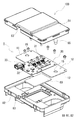
- FIG. 1 is a schematic perspective view showing a circuit configuration body according to Embodiment 1.
- FIG. 1 is a schematic exploded perspective view showing a circuit configuration body according to Embodiment 1.
- FIG. 2 is a schematic longitudinal sectional view showing a main part of the circuit configuration body according to Embodiment 1. It is a schematic longitudinal cross-sectional view which shows the principal part of the circuit board provided with the via hole. It is a schematic longitudinal cross-sectional view which shows the principal part of the circuit board with which the via hole was filled with hole-filling resin. It is a schematic longitudinal cross-sectional view which shows the principal part of the circuit board in which the resist layer was formed.
- 1 is a schematic perspective view showing an electrical junction box according to Embodiment 1.
- FIG. 1 is a schematic exploded perspective view showing an electrical junction box according to Embodiment 1.
- a conventional circuit structure typically, an adhesive sheet in which a thermosetting epoxy adhesive is applied to both surfaces of a polyimide film substrate is used.
- the bus bar and the circuit board are bonded by sandwiching the adhesive sheet between the bus bar and the circuit board and then thermocompression bonding with a hot press device.
- circuit components have problems that it takes time to manufacture because they are thermocompression-bonded, and that the manufacturing cost is high, such as the need for equipment such as a heat press device.
- thermocompression bonding by thermocompression bonding, repeated heating and cooling may cause residual stress in the solder for mounting the circuit board and electronic components, causing deformation in the circuit board and cracking in the solder.
- the epoxy adhesive is easily deteriorated, has poor storage stability, and needs to be stored at a low temperature.
- an object of the present disclosure is to provide a circuit structure having excellent productivity.
- Another object of the present invention is to provide an electrical junction box including the circuit structure.
- thermosetting adhesive eg, an epoxy-based adhesive
- a circuit structure is: A circuit structure in which a circuit board having a control circuit for controlling energization of the power circuit is integrated on a plate-like bus bar constituting the power circuit, A circuit board having circuit patterns formed on both sides and provided with via holes for electrically connecting the circuit patterns; An adhesive sheet interposed between the bus bar and the circuit board and fixing the circuit board on the bus bar; A hole filling resin filled in the via hole; A resist layer formed on at least the surface of the circuit board facing the bus bar so as to cover the via hole filled with the hole-filling resin; The said adhesive sheet is equipped with the base material formed with the insulating material, and the adhesive layer which has adhesiveness at normal temperature on both surfaces of the said base material.
- the bus bar and the circuit board can be pasted at room temperature without thermocompression bonding by the pressure-sensitive adhesive sheet having an adhesive layer having adhesiveness at room temperature, and the circuit board can be easily mounted on the bus bar. Can be fixed. Therefore, thermocompression bonding can be omitted, the manufacturing time can be shortened, and equipment such as a hot press apparatus is not required, and the manufacturing cost can be reduced. Therefore, the circuit structure is excellent in productivity. Furthermore, since thermocompression bonding is not performed, deformation of the circuit board and occurrence of solder cracks due to repeated heating and cooling can be prevented.
- the insulation reliability between the bus bar and the circuit board can be improved by filling the via hole with the resin filling the via hole.
- it is required to ensure electrical insulation between the bus bar and the circuit board.
- a resist layer is formed on the surface of the circuit board that is provided with via holes that faces the bus bar, the resist layer is not formed at the via holes, and the dielectric breakdown voltage between the circuit board and the bus bar is reduced, resulting in electrical insulation. May not be sufficient.
- a resist layer can be formed so as to cover the via hole with the hole filling resin. Therefore, since the resist layer is formed so as to cover the via hole, the circuit configuration body can suppress a decrease in dielectric breakdown voltage due to the via hole, and can secure electrical insulation between the bus bar and the circuit board.
- the pressure-sensitive adhesive layer is made of an acrylic pressure-sensitive adhesive.
- the pressure-sensitive adhesive for the pressure-sensitive adhesive sheet may be any pressure-sensitive adhesive having electrical insulation and adhesiveness at room temperature, and examples thereof include acrylic pressure-sensitive adhesives, silicone-based pressure-sensitive adhesives, and urethane-based pressure-sensitive adhesives.
- the pressure-sensitive adhesive layer is required to have heat resistance against a solder reflow temperature when mounting an electronic component. Furthermore, it is desired that the material is hardly deteriorated at room temperature, has excellent storage stability, and is inexpensive. Acrylic adhesives are suitable because they satisfy these required characteristics and have high adhesiveness.
- the base material is a nonwoven fabric made of cellulose.
- any material may be used as long as it has electrical insulation and heat resistance against the solder reflow temperature, and examples thereof include a nonwoven fabric and a resin film.
- the nonwoven fabric include those containing cellulose fiber, resin fiber, and glass fiber, and examples of the resin fiber include polyimide fiber and polyamideimide fiber.
- the resin film include a polyimide film and a polyamideimide film.
- a cellulose nonwoven fabric in which cellulose fibers are formed into a sheet shape is suitable because it has heat resistance to solder reflow temperature and is relatively inexpensive.
- An electrical junction box is: The circuit structure according to any one of (1) to (3) above; A heat sink attached to the bus bar; A case for housing the circuit structure and the heat sink.
- the electrical junction box is excellent in productivity by including the circuit structure according to one aspect of the present invention. Moreover, since the heat sink is attached to the bus bar of the circuit structure, the electrical junction box can dissipate heat generated in the circuit structure to the heat sink, improving heat dissipation and high reliability.
- the circuit configuration body 1 of Embodiment 1 includes a plate-like bus bar 10 and a circuit board 20, and the circuit board 20 is integrated on the bus bar 10.
- one of the features of the circuit structure 1 according to the first embodiment includes an adhesive sheet 40 between the bus bar 10 and the circuit board 20, and the bus bar 10 and the circuit board are provided by the adhesive sheet 40. 20 is affixed. Further, as shown in FIG.
- the filling resin 25 filled in the via hole 23 provided in the circuit board 20 and the filling resin 25 filled in at least the surface of the circuit board 20 facing the bus bar 10 are provided.
- the bus bar 10 is a plate-like component that constitutes a power circuit.
- the bus bar 10 includes a plurality of bus bar pieces 11 to 13, and the bus bar pieces 11 to 13 are arranged in a predetermined layout on the same plane.
- the bus bar 10 (bus bar pieces 11 to 13) is formed of a conductive metal plate, and specifically is formed by cutting a copper plate material into a predetermined shape.
- the size of the bus bar 10 (the bus bar pieces 11 to 13) is set to a size suitable for the amount of energization and heat dissipation, and the thickness is, for example, about 0.5 mm to 1.0 mm.
- a wire harness 90 see FIG.
- terminal insertion holes 15 through which power supply terminals 85 (see FIGS. 7 and 8) to be described later are inserted are formed in the bus bar pieces 11 and 12, respectively, and the bus bar pieces 11 and 12 are connected via the power supply terminals 85. And electrically connected to the wire harness 90.
- the circuit board 20 is disposed on the bus bar 10 as shown in FIGS. 1 to 3 and has a control circuit that controls energization of the power circuit.
- the circuit board 20 is a double-sided board (multilayer board) having circuit patterns 21 and 22 formed on both sides, and is provided with via holes 23 for electrically connecting the circuit patterns 21 and 22 to each other. Yes.
- the circuit board 20 is specifically a printed circuit board on which circuit patterns 21 and 22 are printed on an insulating substrate 28, and the circuit patterns 21 and 22 are formed of copper foil.
- the circuit patterns 21 and 22 are covered with resist layers 26 and 27, which will be described later.
- An external electronic control unit (not shown) is connected to the circuit board 20.
- the microcomputer 32 is a control element that controls the FET 31 and the like.
- the control connector 33 is a connector for connecting the electronic control unit, and the electronic component is driven based on a control signal from the electronic control unit.
- the circuit pattern 21 on the upper surface of the circuit board 20 is provided with lands 24 for soldering each component (not shown in FIG. 3).
- the control circuit includes circuit patterns 21 and 22 formed on the circuit board 20 and electronic components mounted on the circuit board 20.
- another part of the terminal of the FET 31 is directly solder-bonded to the bus bar 10, so that the portion of the circuit board 20 where the FET 31 is disposed is provided for a part corresponding to the FET 31, as shown in FIG. An opening 29 is formed.
- the via hole 23 of the circuit board 20 is filled with a hole filling resin 25.
- the hole filling resin 25 is filled into the via hole 23 when the circuit board 20 is manufactured (see FIG. 5).
- the hole filling resin 25 is an insulating resin, and in this example, is an epoxy resin.
- the hole filling resin 25 is filled so as to be flush with the upper and lower openings of the via hole 23.
- a resist layer 26 is formed on the lower surface of the circuit board 20 (the surface facing the bus bar 10) so as to cover the via hole 23 filled with the hole filling resin 25.
- the resist layer 27 is also formed on the upper surface of the circuit board 20, and the land 24 is not covered with the resist layer 27.
- the resist layers 26 and 27 are for protecting the circuit patterns 21 and 22, maintaining electrical insulation, and preventing solder from adhering to unnecessary portions when mounting electronic components.
- the resist layers 26 and 27 are formed by filling a via hole 23 with a filling resin 25 and then applying a resist ink when the circuit board 20 is manufactured (see FIG. 6).
- the resist layers 26 and 27 are made of an insulating resin, which is an epoxy resin in this example.
- the thickness of the resist layer 26 is preferably, for example, 5 ⁇ m or more, more preferably 25 ⁇ m or more, from the viewpoint of ensuring electrical insulation between the bus bar 10 and the circuit board 20 (circuit pattern 22).
- the upper limit of the thickness of the resist layer 26 is, for example, 65 ⁇ m from the viewpoint of adhesion to the circuit board 20 and workability.
- the insulation resistance of the resist layer 26 is, for example, 500 M ⁇ or more.
- the adhesive sheet 40 is interposed between the bus bar 10 and the circuit board 20 (resist layer 26), and fixes the circuit board 20 on the bus bar 10.
- the pressure-sensitive adhesive sheet 40 includes a base material 41 formed of an insulating material, and a pressure-sensitive adhesive layer 42 having adhesiveness at normal temperature on both surfaces of the base material 41.
- the base material 41 of the pressure-sensitive adhesive sheet 40 is formed of a material having heat resistance and electrical insulation against a solder reflow temperature (for example, 260 ° C.).
- a nonwoven fabric including cellulose fiber, resin fiber, glass fiber, polyimide, polyamideimide For example, a resin film.
- the resin fiber include polyimide fiber and polyamideimide fiber.
- the base material 41 is a nonwoven fabric made of cellulose.
- the thickness of the base material 41 may be selected as appropriate so as to ensure electrical insulation between the bus bar 10 and the circuit board 20, and the thickness of the pressure-sensitive adhesive sheet 40 including the pressure-sensitive adhesive layer 42 is, for example, 50 ⁇ m or more. To do.
- the pressure-sensitive adhesive layer 42 of the pressure-sensitive adhesive sheet 40 is formed of a pressure-sensitive adhesive having heat resistance against solder reflow temperature and electrical insulation, and having adhesiveness at room temperature.
- the pressure-sensitive adhesive include acrylic pressure-sensitive adhesives and silicone-based pressure-sensitive adhesives. Agents, urethane adhesives, and the like. Among them, an acrylic pressure-sensitive adhesive containing an acrylic polymer is practical because it has high tackiness, can be stored at room temperature, has excellent storability, and is inexpensive.
- the pressure-sensitive adhesive layer 42 is made of an acrylic pressure-sensitive adhesive.
- the pressure-sensitive adhesive layer 42 is formed by applying a pressure-sensitive adhesive to both surfaces of the base material 41.
- a component opening 49 corresponding to the FET 31 is formed in the adhesive sheet 40 at the same position as the component opening 29 of the circuit board 20.
- a bus bar 10, a circuit board 20, and an adhesive sheet 40 are prepared (see FIG. 2).
- the bus bar 10 is produced by cutting an oxygen-free copper plate into a predetermined shape. Specifically, an oxygen-free copper plate material is punched out to produce a bus bar 10 in which bus bar pieces 11 to 13 having a predetermined shape are arranged as shown in FIG.
- the circuit board 20 is manufactured as follows. Component openings 29 (see FIG. 2) and the like are formed in a copper clad laminate in which copper foils are laminated on both surfaces of an insulating substrate 28 (see FIG. 3), and a substrate material processed into a predetermined shape is prepared. Then, as shown in FIG. 4, circuit patterns 21 and 22 and via holes 23 are formed in the substrate material. Specifically, a through-hole is drilled at a predetermined position of the substrate material, and copper plating is applied to the inner surface of the hole to form a via hole 23 that electrically connects the copper foils on both sides, and the copper foils on both sides Are etched to form circuit patterns 21 and 22.
- the via hole 23 is filled with an epoxy resin and cured to form a hole filling resin 25.
- resist resin 26 and 27 are formed by applying an epoxy resin resist ink on both surfaces of the circuit board 20 so as to cover the via holes 23.
- the resist layer 27 is formed, a portion of the land 24 or the like not covered with the resist layer 27 is prevented from being formed by masking or the like.
- the circuit board 20 is manufactured as described above.
- the pressure-sensitive adhesive sheet 40 is a pressure-sensitive adhesive sheet having a pressure-sensitive adhesive layer 42 (see FIG. 3) made of an acrylic pressure-sensitive adhesive on both surfaces of a cellulose nonwoven fabric base 41 (see FIG. 3), as shown in FIG. Cut to make.
- bus bar 10 and the circuit board 20 are bonded together with the adhesive sheet 40, and the circuit board 20 is fixed on the bus bar 10 (see FIG. 2).
- the adhesive sheet 40 is sandwiched between the bus bar 10 and the circuit board 20, and the bus bar 10 and the circuit board 20 are attached. Thereby, the bus bar 10 and the circuit board 20 are integrated.
- the circuit configuration body 1 of Embodiment 1 has the following effects.
- the circuit configuration body 1 has the bus bar 10 and the circuit board 20 attached to each side of the base material 41 by an adhesive sheet 40 having an adhesive layer 42 having adhesiveness at room temperature. Yes. Therefore, the bus bar 10 and the circuit board 20 can be pasted at room temperature, and there is no need for thermocompression bonding as in the prior art. Accordingly, the circuit assembly 1 can reduce the time required for manufacturing by omitting thermocompression bonding as compared with the prior art, and also does not require equipment such as a heat press device, thereby improving productivity and simplifying manufacturing equipment. It is possible, and it is excellent in productivity at low cost. In addition, deformation of the circuit board 20 and generation of solder cracks due to residual stress caused by thermocompression bonding can be prevented, and reliability is improved.
- the via hole 23 provided in the circuit board 20 is filled with the filling resin 25, and the resist layer 26 is provided on the surface of the circuit board 20 facing the bus bar 10. Is formed. Therefore, the resist layer 26 can be formed to cover the via hole 23 by filling the via hole 23 with the hole filling resin 25.
- the resist layer 26 may not be formed in the portion of the via hole 23. Therefore, the circuit structure 1 has the resist layer 26 formed so as to cover the via hole 23 filled with the hole filling resin 25, so that the circuit structure 1 and the circuit board 1 and the circuit board 1 are compared with the case where the hole filling resin 25 is not filled.
- the dielectric breakdown voltage with the substrate 20 is increased. Therefore, the electrical reliability between the bus bar 10 and the circuit board 20 is high, and electrical insulation can be ensured.
- the circuit board 20 can be firmly fixed on the bus bar 10.
- An acrylic pressure-sensitive adhesive has high adhesiveness and heat resistance, and can be stored at room temperature, is excellent in storage stability, and is inexpensive. Therefore, it is possible to improve productivity and reduce manufacturing costs.
- the base material 41 of the pressure-sensitive adhesive sheet 40 is a cellulose nonwoven fabric, the cost of the pressure-sensitive adhesive sheet 40 can be reduced, and the manufacturing cost can be reduced.
- an adhesive sheet used in a conventional circuit structure is a polyimide film, and is expensive, whereas a cellulose nonwoven fabric is inexpensive. Therefore, member costs can be reduced by using a pressure-sensitive adhesive sheet formed of a nonwoven fabric made of cellulose as compared with the case of using a conventional adhesive sheet.
- the electrical junction box 100 of Embodiment 1 is demonstrated with reference to FIG.7 and FIG.8.
- the electrical junction box 100 of the first embodiment includes a circuit configuration body 1, a heat sink 60, and a case 80.
- FIG. 7 is a view as seen from the lower side of the electrical junction box 100, and is upside down from FIG.
- the configuration of the electrical junction box 100 will be described in detail.
- the circuit structure 1 shown in FIG. 8 is the same as the circuit structure 1 of the first embodiment shown in FIG. 1 described above, and the same components are denoted by the same reference numerals and description thereof is omitted.
- the heat sink 60 is attached to the bus bar 10 of the circuit structure 1.
- the heat sink 60 is made of, for example, a metal material with high thermal conductivity such as aluminum or copper.
- the heat sink 60 is an aluminum plate.
- the shape of the heat sink 60 is not particularly limited, and may be, for example, a block shape in addition to a plate shape.
- the main role of the heat sink 60 is to prevent the temperature of the electronic component (FET 31 or the like) mounted on the circuit structure 1 or the temperature of the solder for mounting the electronic component from exceeding the allowable temperature.
- the size of the heat sink 60 may be a size suitable for heat dissipation.
- the attachment of the heat sink 60 to the circuit structure 1 (bus bar 10) is, for example, pasted with an adhesive sheet having the same configuration as the adhesive sheet 40 (see FIG. 3) used in the circuit structure 1.
- the heat sink 60 may be adhered and pasted to the circuit component 1 (bus bar 10) using an adhesive or an adhesive sheet in which an adhesive is applied to both surfaces of the substrate.
- thermocompression bonding is not necessary, so that it can be produced at low cost and has excellent productivity.
- the case 80 accommodates the circuit structure 1 and the heat sink 60.
- the case 80 includes an upper case 81 and a lower case 82. Inside the upper case 81, a rod-shaped power terminal 85 extending toward the lower case 82 is provided.
- the power supply terminal 85 is inserted into the terminal insertion hole 15 formed in the bus bar 10 (bus bar pieces 11, 12) of the circuit structure 1 and is electrically connected to the bus bar 10.
- the power terminal 85 protrudes to the outside of the case 80 through a through-hole formed in the lower case 82, and the wire harness 90 is attached to the end of the power terminal 85 that protrudes to the outside from the case 80. It is done. Thereby, the bus bar 10 is electrically connected to the wire harness 90 via the power supply terminal 85.
- a connector opening 83 is formed in the case 80 so that the control connector 33 of the circuit structure 1 is exposed to the outside of the case 80.
- the circuit component 1 After affixing the heat sink 60 to the lower surface of the bus bar 10 of the circuit component 1, the circuit component 1 is fixed to the inside of the lower case 82 with screws. Then, the case 80 is assembled by fitting the upper case 81 into the lower case 82. As described above, the electrical junction box 100 shown in FIG. 7 is obtained.
- Sample 1 is the above-described circuit configuration of the first embodiment.
- a pressure-sensitive adhesive sheet in which an acrylic pressure-sensitive adhesive was applied to both surfaces of a cellulose nonwoven fabric base material was used, and a bus bar and a circuit board were attached to each other with the pressure-sensitive adhesive sheet.
- the via hole of the circuit board was filled with an epoxy resin filling resin, and an epoxy resin resist layer was formed on the lower surface of the circuit board so as to cover the via hole.
- the thickness of the pressure-sensitive adhesive sheet was 50 ⁇ m, and the thickness of the resist layer was 25 ⁇ m.
- Sample 2 was prepared in the same manner as Sample 1 except that the via hole of the circuit board was not filled with epoxy resin filling resin.
- Sample 3 was an adhesive sheet in which an epoxy adhesive was applied to both surfaces of a polyimide film substrate instead of the adhesive sheet of Sample 1. Then, the bus bar and the circuit board were bonded by thermocompression bonding with an adhesive sheet sandwiched between the circuit board and the circuit board. Further, in the circuit structure of sample 3, as in sample 2, the via hole of the circuit board is not filled with the epoxy resin filling resin. The thickness of the base material of the adhesive sheet is 25 ⁇ m.
- the circuit structure of Sample 1 did not cause dielectric breakdown up to 2.0 V, and had high electrical insulation of DC 2 kV or higher.
- the circuit structure of sample 2 had dielectric breakdown at 1.8 V, the dielectric breakdown voltage was lower than that of sample 1, and the electrical insulation was reduced.
- the via hole is filled with a hole filling resin, and the resist layer is formed so as to cover the via hole filled with the hole filling resin, so that sufficient electrical insulation is ensured by the resist layer and the adhesive sheet. It is thought that.
- sample 3 did not cause dielectric breakdown up to 2.0 V, and had high electrical insulation like sample 1. However, since it is necessary to perform thermocompression bonding with the sample 3, the work is complicated and inferior in productivity as compared with the sample 1. In Sample 3, since an expensive polyimide film is used as the base material of the adhesive sheet, the price of the adhesive sheet is high. On the other hand, in Sample 1, since the base material of the pressure-sensitive adhesive sheet is a cellulose nonwoven fabric, and the pressure-sensitive adhesive sheet is cheaper than the adhesive sheet, the member cost can be reduced.
- circuit structure and the electrical junction box according to the embodiment of the present invention can be suitably used for an electrical junction box for automobiles.
Landscapes
- Engineering & Computer Science (AREA)
- Microelectronics & Electronic Packaging (AREA)
- Architecture (AREA)
- Civil Engineering (AREA)
- Structural Engineering (AREA)
- Mechanical Engineering (AREA)
- Connection Or Junction Boxes (AREA)
- Structure Of Printed Boards (AREA)
Priority Applications (3)
| Application Number | Priority Date | Filing Date | Title |
|---|---|---|---|
| DE112016005766.0T DE112016005766B4 (de) | 2015-12-16 | 2016-12-07 | Schaltungsanordnung und elektrischer anschlusskasten |
| CN201680074201.3A CN108432073B (zh) | 2015-12-16 | 2016-12-07 | 电路结构体及电气接线盒 |
| US15/775,952 US20180370463A1 (en) | 2015-12-16 | 2016-12-07 | Circuit assembly and electrical junction box |
Applications Claiming Priority (2)
| Application Number | Priority Date | Filing Date | Title |
|---|---|---|---|
| JP2015-244888 | 2015-12-16 | ||
| JP2015244888A JP6443688B2 (ja) | 2015-12-16 | 2015-12-16 | 回路構成体、及び電気接続箱 |
Publications (1)
| Publication Number | Publication Date |
|---|---|
| WO2017104517A1 true WO2017104517A1 (ja) | 2017-06-22 |
Family
ID=59056379
Family Applications (1)
| Application Number | Title | Priority Date | Filing Date |
|---|---|---|---|
| PCT/JP2016/086460 Ceased WO2017104517A1 (ja) | 2015-12-16 | 2016-12-07 | 回路構成体、及び電気接続箱 |
Country Status (5)
| Country | Link |
|---|---|
| US (1) | US20180370463A1 (enExample) |
| JP (1) | JP6443688B2 (enExample) |
| CN (1) | CN108432073B (enExample) |
| DE (1) | DE112016005766B4 (enExample) |
| WO (1) | WO2017104517A1 (enExample) |
Cited By (1)
| Publication number | Priority date | Publication date | Assignee | Title |
|---|---|---|---|---|
| WO2020049976A1 (ja) * | 2018-09-03 | 2020-03-12 | 株式会社オートネットワーク技術研究所 | 回路構造体及び電気接続箱 |
Families Citing this family (9)
| Publication number | Priority date | Publication date | Assignee | Title |
|---|---|---|---|---|
| JP6548146B2 (ja) * | 2016-05-17 | 2019-07-24 | 株式会社オートネットワーク技術研究所 | 回路構成体 |
| JP6499124B2 (ja) * | 2016-06-30 | 2019-04-10 | 矢崎総業株式会社 | 導電部材および電気接続箱 |
| EP3557602B1 (en) * | 2016-12-15 | 2024-04-24 | Amogreentech Co., Ltd. | Power relay assembly |
| EP3605761B1 (en) * | 2017-03-24 | 2021-12-08 | Yazaki Corporation | Electrical junction box and wiring harness |
| JP7001960B2 (ja) * | 2018-03-23 | 2022-01-20 | 株式会社オートネットワーク技術研究所 | 回路構成体 |
| DE102019207520A1 (de) * | 2018-06-28 | 2020-01-02 | Robert Bosch Engineering And Business Solutions Private Limited | Elektronische steuereinheit (ecu) der art eines direktkontaktsystems (dcs) |
| JP6682027B1 (ja) * | 2019-04-22 | 2020-04-15 | 三菱電機株式会社 | バスバーモジュール |
| CN111343553B (zh) * | 2020-04-09 | 2021-02-19 | 江苏普诺威电子股份有限公司 | 具有高对准精度的mems麦克风腔体板及其制作方法 |
| GB2615997B (en) | 2020-11-09 | 2024-08-28 | Eae Elektrik Asansoer Enduestrisi Insaat Sanayi Ve Ticaret Anonim Sirketi | Filling device for the joint in energy distribution lines |
Citations (3)
| Publication number | Priority date | Publication date | Assignee | Title |
|---|---|---|---|---|
| JP2005294741A (ja) * | 2004-04-05 | 2005-10-20 | Auto Network Gijutsu Kenkyusho:Kk | 電気接続箱 |
| JP2006005107A (ja) * | 2004-06-16 | 2006-01-05 | Auto Network Gijutsu Kenkyusho:Kk | 回路構成体 |
| JP2015139289A (ja) * | 2014-01-22 | 2015-07-30 | 株式会社オートネットワーク技術研究所 | スイッチング基板 |
Family Cites Families (13)
| Publication number | Priority date | Publication date | Assignee | Title |
|---|---|---|---|---|
| US5055967A (en) * | 1988-10-26 | 1991-10-08 | Texas Instruments Incorporated | Substrate for an electrical circuit system and a circuit system using that substrate |
| EP1980886A3 (en) * | 2002-04-01 | 2008-11-12 | Ibiden Co., Ltd. | Optical communication device and optical communication device manufacturing method |
| JP2004328939A (ja) * | 2003-04-25 | 2004-11-18 | Sumitomo Wiring Syst Ltd | 電気接続箱 |
| JP2005117719A (ja) * | 2003-10-03 | 2005-04-28 | Auto Network Gijutsu Kenkyusho:Kk | 回路構成体製造用接着シート及び接着シートを用いた回路構成体の製造方法 |
| JP2006211776A (ja) * | 2005-01-26 | 2006-08-10 | Sumitomo Wiring Syst Ltd | 電気接続箱 |
| WO2006109597A1 (ja) * | 2005-04-11 | 2006-10-19 | Autonetworks Technologies, Ltd. | 電気接続箱 |
| JP2007049036A (ja) * | 2005-08-11 | 2007-02-22 | Nitto Denko Corp | 配線回路基板 |
| JP4608422B2 (ja) * | 2005-12-05 | 2011-01-12 | 共同技研化学株式会社 | 粘接着フィルム |
| JP5448409B2 (ja) * | 2008-10-16 | 2014-03-19 | 日東電工株式会社 | 粘着剤組成物および粘着シート |
| JP5542360B2 (ja) * | 2009-03-30 | 2014-07-09 | 太陽ホールディングス株式会社 | プリント配線板 |
| DE102009053998A1 (de) | 2009-11-19 | 2011-05-26 | Still Gmbh | Umrichter, insbesondere mehrphasiger Drehstromumrichter |
| JP5901923B2 (ja) * | 2011-09-30 | 2016-04-13 | 太陽インキ製造株式会社 | 熱硬化性樹脂充填材及びプリント配線板 |
| DE102013219192A1 (de) | 2013-09-24 | 2015-03-26 | Conti Temic Microelectronic Gmbh | Leistungsmodul, Stromrichter und Antriebsanordnung mit einem Leistungsmodul |
-
2015
- 2015-12-16 JP JP2015244888A patent/JP6443688B2/ja not_active Expired - Fee Related
-
2016
- 2016-12-07 WO PCT/JP2016/086460 patent/WO2017104517A1/ja not_active Ceased
- 2016-12-07 US US15/775,952 patent/US20180370463A1/en not_active Abandoned
- 2016-12-07 DE DE112016005766.0T patent/DE112016005766B4/de not_active Expired - Fee Related
- 2016-12-07 CN CN201680074201.3A patent/CN108432073B/zh not_active Expired - Fee Related
Patent Citations (3)
| Publication number | Priority date | Publication date | Assignee | Title |
|---|---|---|---|---|
| JP2005294741A (ja) * | 2004-04-05 | 2005-10-20 | Auto Network Gijutsu Kenkyusho:Kk | 電気接続箱 |
| JP2006005107A (ja) * | 2004-06-16 | 2006-01-05 | Auto Network Gijutsu Kenkyusho:Kk | 回路構成体 |
| JP2015139289A (ja) * | 2014-01-22 | 2015-07-30 | 株式会社オートネットワーク技術研究所 | スイッチング基板 |
Cited By (2)
| Publication number | Priority date | Publication date | Assignee | Title |
|---|---|---|---|---|
| WO2020049976A1 (ja) * | 2018-09-03 | 2020-03-12 | 株式会社オートネットワーク技術研究所 | 回路構造体及び電気接続箱 |
| JP2020038882A (ja) * | 2018-09-03 | 2020-03-12 | 株式会社オートネットワーク技術研究所 | 回路構造体及び電気接続箱 |
Also Published As
| Publication number | Publication date |
|---|---|
| JP2017112708A (ja) | 2017-06-22 |
| JP6443688B2 (ja) | 2018-12-26 |
| DE112016005766T5 (de) | 2018-08-30 |
| US20180370463A1 (en) | 2018-12-27 |
| CN108432073B (zh) | 2021-07-06 |
| CN108432073A (zh) | 2018-08-21 |
| DE112016005766B4 (de) | 2022-06-09 |
Similar Documents
| Publication | Publication Date | Title |
|---|---|---|
| JP6443688B2 (ja) | 回路構成体、及び電気接続箱 | |
| CN108370142B (zh) | 电路结构体及电气接线盒 | |
| US10194523B2 (en) | Circuit assembly, electrical junction box, and manufacturing method for circuit assembly | |
| US10164417B2 (en) | Circuit assembly and electrical junction box | |
| US7903417B2 (en) | Electrical circuit assembly for high-power electronics | |
| US20070010086A1 (en) | Circuit board with a through hole wire and manufacturing method thereof | |
| CN105580227A (zh) | 电路构成体 | |
| JP6852649B2 (ja) | 回路構成体及び回路構成体の製造方法 | |
| JP6307093B2 (ja) | 電子制御装置、電子制御装置の製造方法 | |
| AU2008201050B2 (en) | Electronic-component-mounting board | |
| CN102474976B (zh) | 布线基板以及布线基板的制造方法 | |
| WO2017199837A1 (ja) | 回路構成体 | |
| JP6119664B2 (ja) | 回路構成体および電気接続箱 | |
| JP6065806B2 (ja) | 回路構成体及び回路構成体の製造方法 | |
| JP6403741B2 (ja) | 表面実装型半導体パッケージ装置 | |
| US20080084671A1 (en) | Electrical circuit assembly for high-power electronics | |
| JP2004259904A (ja) | 電子回路装置の回路基板およびその製造方法 | |
| JP2008092726A (ja) | 回路材および回路材の形成方法 | |
| JP2011199002A (ja) | プリント基板及びその製造方法 | |
| KR20240171248A (ko) | 컨트롤러의 방열구조 | |
| JP2015012159A (ja) | 電子装置およびその製造方法 | |
| JP2006288118A (ja) | スイッチングユニット | |
| JP2013165172A (ja) | 配線基板およびその製造方法 |
Legal Events
| Date | Code | Title | Description |
|---|---|---|---|
| 121 | Ep: the epo has been informed by wipo that ep was designated in this application |
Ref document number: 16875497 Country of ref document: EP Kind code of ref document: A1 |
|
| WWE | Wipo information: entry into national phase |
Ref document number: 112016005766 Country of ref document: DE |
|
| 122 | Ep: pct application non-entry in european phase |
Ref document number: 16875497 Country of ref document: EP Kind code of ref document: A1 |