WO2017104517A1 - Circuit structure, and electrical connection box - Google Patents
Circuit structure, and electrical connection box Download PDFInfo
- Publication number
- WO2017104517A1 WO2017104517A1 PCT/JP2016/086460 JP2016086460W WO2017104517A1 WO 2017104517 A1 WO2017104517 A1 WO 2017104517A1 JP 2016086460 W JP2016086460 W JP 2016086460W WO 2017104517 A1 WO2017104517 A1 WO 2017104517A1
- Authority
- WO
- WIPO (PCT)
- Prior art keywords
- circuit
- circuit board
- bus bar
- circuit structure
- adhesive sheet
- Prior art date
Links
Images


Classifications
-
- B—PERFORMING OPERATIONS; TRANSPORTING
- B60—VEHICLES IN GENERAL
- B60R—VEHICLES, VEHICLE FITTINGS, OR VEHICLE PARTS, NOT OTHERWISE PROVIDED FOR
- B60R16/00—Electric or fluid circuits specially adapted for vehicles and not otherwise provided for; Arrangement of elements of electric or fluid circuits specially adapted for vehicles and not otherwise provided for
- B60R16/02—Electric or fluid circuits specially adapted for vehicles and not otherwise provided for; Arrangement of elements of electric or fluid circuits specially adapted for vehicles and not otherwise provided for electric constitutive elements
- B60R16/023—Electric or fluid circuits specially adapted for vehicles and not otherwise provided for; Arrangement of elements of electric or fluid circuits specially adapted for vehicles and not otherwise provided for electric constitutive elements for transmission of signals between vehicle parts or subsystems
- B60R16/0239—Electronic boxes
-
- H—ELECTRICITY
- H02—GENERATION; CONVERSION OR DISTRIBUTION OF ELECTRIC POWER
- H02G—INSTALLATION OF ELECTRIC CABLES OR LINES, OR OF COMBINED OPTICAL AND ELECTRIC CABLES OR LINES
- H02G3/00—Installations of electric cables or lines or protective tubing therefor in or on buildings, equivalent structures or vehicles
- H02G3/02—Details
- H02G3/08—Distribution boxes; Connection or junction boxes
- H02G3/16—Distribution boxes; Connection or junction boxes structurally associated with support for line-connecting terminals within the box
-
- B—PERFORMING OPERATIONS; TRANSPORTING
- B60—VEHICLES IN GENERAL
- B60R—VEHICLES, VEHICLE FITTINGS, OR VEHICLE PARTS, NOT OTHERWISE PROVIDED FOR
- B60R16/00—Electric or fluid circuits specially adapted for vehicles and not otherwise provided for; Arrangement of elements of electric or fluid circuits specially adapted for vehicles and not otherwise provided for
- B60R16/02—Electric or fluid circuits specially adapted for vehicles and not otherwise provided for; Arrangement of elements of electric or fluid circuits specially adapted for vehicles and not otherwise provided for electric constitutive elements
- B60R16/023—Electric or fluid circuits specially adapted for vehicles and not otherwise provided for; Arrangement of elements of electric or fluid circuits specially adapted for vehicles and not otherwise provided for electric constitutive elements for transmission of signals between vehicle parts or subsystems
- B60R16/0238—Electrical distribution centers
-
- H—ELECTRICITY
- H02—GENERATION; CONVERSION OR DISTRIBUTION OF ELECTRIC POWER
- H02G—INSTALLATION OF ELECTRIC CABLES OR LINES, OR OF COMBINED OPTICAL AND ELECTRIC CABLES OR LINES
- H02G3/00—Installations of electric cables or lines or protective tubing therefor in or on buildings, equivalent structures or vehicles
- H02G3/02—Details
- H02G3/03—Cooling
-
- H—ELECTRICITY
- H05—ELECTRIC TECHNIQUES NOT OTHERWISE PROVIDED FOR
- H05K—PRINTED CIRCUITS; CASINGS OR CONSTRUCTIONAL DETAILS OF ELECTRIC APPARATUS; MANUFACTURE OF ASSEMBLAGES OF ELECTRICAL COMPONENTS
- H05K1/00—Printed circuits
- H05K1/02—Details
- H05K1/0201—Thermal arrangements, e.g. for cooling, heating or preventing overheating
- H05K1/0203—Cooling of mounted components
-
- H—ELECTRICITY
- H05—ELECTRIC TECHNIQUES NOT OTHERWISE PROVIDED FOR
- H05K—PRINTED CIRCUITS; CASINGS OR CONSTRUCTIONAL DETAILS OF ELECTRIC APPARATUS; MANUFACTURE OF ASSEMBLAGES OF ELECTRICAL COMPONENTS
- H05K1/00—Printed circuits
- H05K1/02—Details
- H05K1/0213—Electrical arrangements not otherwise provided for
- H05K1/0263—High current adaptations, e.g. printed high current conductors or using auxiliary non-printed means; Fine and coarse circuit patterns on one circuit board
-
- H—ELECTRICITY
- H05—ELECTRIC TECHNIQUES NOT OTHERWISE PROVIDED FOR
- H05K—PRINTED CIRCUITS; CASINGS OR CONSTRUCTIONAL DETAILS OF ELECTRIC APPARATUS; MANUFACTURE OF ASSEMBLAGES OF ELECTRICAL COMPONENTS
- H05K1/00—Printed circuits
- H05K1/02—Details
- H05K1/11—Printed elements for providing electric connections to or between printed circuits
- H05K1/115—Via connections; Lands around holes or via connections
-
- H—ELECTRICITY
- H05—ELECTRIC TECHNIQUES NOT OTHERWISE PROVIDED FOR
- H05K—PRINTED CIRCUITS; CASINGS OR CONSTRUCTIONAL DETAILS OF ELECTRIC APPARATUS; MANUFACTURE OF ASSEMBLAGES OF ELECTRICAL COMPONENTS
- H05K1/00—Printed circuits
- H05K1/02—Details
- H05K1/03—Use of materials for the substrate
- H05K1/0386—Paper sheets
-
- H—ELECTRICITY
- H05—ELECTRIC TECHNIQUES NOT OTHERWISE PROVIDED FOR
- H05K—PRINTED CIRCUITS; CASINGS OR CONSTRUCTIONAL DETAILS OF ELECTRIC APPARATUS; MANUFACTURE OF ASSEMBLAGES OF ELECTRICAL COMPONENTS
- H05K2201/00—Indexing scheme relating to printed circuits covered by H05K1/00
- H05K2201/09—Shape and layout
- H05K2201/09209—Shape and layout details of conductors
- H05K2201/095—Conductive through-holes or vias
- H05K2201/0959—Plated through-holes or plated blind vias filled with insulating material
-
- H—ELECTRICITY
- H05—ELECTRIC TECHNIQUES NOT OTHERWISE PROVIDED FOR
- H05K—PRINTED CIRCUITS; CASINGS OR CONSTRUCTIONAL DETAILS OF ELECTRIC APPARATUS; MANUFACTURE OF ASSEMBLAGES OF ELECTRICAL COMPONENTS
- H05K2201/00—Indexing scheme relating to printed circuits covered by H05K1/00
- H05K2201/10—Details of components or other objects attached to or integrated in a printed circuit board
- H05K2201/10007—Types of components
- H05K2201/10166—Transistor
-
- H—ELECTRICITY
- H05—ELECTRIC TECHNIQUES NOT OTHERWISE PROVIDED FOR
- H05K—PRINTED CIRCUITS; CASINGS OR CONSTRUCTIONAL DETAILS OF ELECTRIC APPARATUS; MANUFACTURE OF ASSEMBLAGES OF ELECTRICAL COMPONENTS
- H05K2201/00—Indexing scheme relating to printed circuits covered by H05K1/00
- H05K2201/10—Details of components or other objects attached to or integrated in a printed circuit board
- H05K2201/10227—Other objects, e.g. metallic pieces
- H05K2201/10272—Busbars, i.e. thick metal bars mounted on the PCB as high-current conductors
-
- H—ELECTRICITY
- H05—ELECTRIC TECHNIQUES NOT OTHERWISE PROVIDED FOR
- H05K—PRINTED CIRCUITS; CASINGS OR CONSTRUCTIONAL DETAILS OF ELECTRIC APPARATUS; MANUFACTURE OF ASSEMBLAGES OF ELECTRICAL COMPONENTS
- H05K3/00—Apparatus or processes for manufacturing printed circuits
- H05K3/0058—Laminating printed circuit boards onto other substrates, e.g. metallic substrates
- H05K3/0061—Laminating printed circuit boards onto other substrates, e.g. metallic substrates onto a metallic substrate, e.g. a heat sink
Definitions
- the present invention relates to a circuit structure and an electrical junction box.
- This application claims priority based on Japanese Patent Application No. 2015-244888 filed on December 16, 2015, and incorporates all the content described in the above Japanese application.
- an electric junction box also called a power distributor
- the electrical junction box includes a bus bar that is connected to a power source and forms a power circuit, and a circuit board that has a control circuit that controls energization of the power circuit.
- the control circuit includes a circuit pattern formed on a circuit board, and electronic components such as a switching element such as a relay or FET (Field effect transistor), or a control element such as a microcomputer or a control IC (Integrated Circuit).
- Patent Document 1 describes a circuit structure manufactured by bonding a bus bar and a circuit board with an adhesive sheet.
- the circuit structure of the present disclosure is: A circuit structure in which a circuit board having a control circuit for controlling energization of the power circuit is integrated on a plate-like bus bar constituting the power circuit, A circuit board having circuit patterns formed on both sides and provided with via holes for electrically connecting the circuit patterns; An adhesive sheet interposed between the bus bar and the circuit board and fixing the circuit board on the bus bar; A hole filling resin filled in the via hole; A resist layer formed on at least the surface of the circuit board facing the bus bar so as to cover the via hole filled with the hole-filling resin;
- the said adhesive sheet is equipped with the base material formed with the insulating material, and the adhesive layer which has adhesiveness at normal temperature on both surfaces of the said base material.
- the electrical junction box of the present disclosure is: The circuit structure of the present disclosure; A heat sink attached to the bus bar; A case for housing the circuit structure and the heat sink.
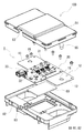
- FIG. 1 is a schematic perspective view showing a circuit configuration body according to Embodiment 1.
- FIG. 1 is a schematic exploded perspective view showing a circuit configuration body according to Embodiment 1.
- FIG. 2 is a schematic longitudinal sectional view showing a main part of the circuit configuration body according to Embodiment 1. It is a schematic longitudinal cross-sectional view which shows the principal part of the circuit board provided with the via hole. It is a schematic longitudinal cross-sectional view which shows the principal part of the circuit board with which the via hole was filled with hole-filling resin. It is a schematic longitudinal cross-sectional view which shows the principal part of the circuit board in which the resist layer was formed.
- 1 is a schematic perspective view showing an electrical junction box according to Embodiment 1.
- FIG. 1 is a schematic exploded perspective view showing an electrical junction box according to Embodiment 1.
- a conventional circuit structure typically, an adhesive sheet in which a thermosetting epoxy adhesive is applied to both surfaces of a polyimide film substrate is used.
- the bus bar and the circuit board are bonded by sandwiching the adhesive sheet between the bus bar and the circuit board and then thermocompression bonding with a hot press device.
- circuit components have problems that it takes time to manufacture because they are thermocompression-bonded, and that the manufacturing cost is high, such as the need for equipment such as a heat press device.
- thermocompression bonding by thermocompression bonding, repeated heating and cooling may cause residual stress in the solder for mounting the circuit board and electronic components, causing deformation in the circuit board and cracking in the solder.
- the epoxy adhesive is easily deteriorated, has poor storage stability, and needs to be stored at a low temperature.
- an object of the present disclosure is to provide a circuit structure having excellent productivity.
- Another object of the present invention is to provide an electrical junction box including the circuit structure.
- thermosetting adhesive eg, an epoxy-based adhesive
- a circuit structure is: A circuit structure in which a circuit board having a control circuit for controlling energization of the power circuit is integrated on a plate-like bus bar constituting the power circuit, A circuit board having circuit patterns formed on both sides and provided with via holes for electrically connecting the circuit patterns; An adhesive sheet interposed between the bus bar and the circuit board and fixing the circuit board on the bus bar; A hole filling resin filled in the via hole; A resist layer formed on at least the surface of the circuit board facing the bus bar so as to cover the via hole filled with the hole-filling resin; The said adhesive sheet is equipped with the base material formed with the insulating material, and the adhesive layer which has adhesiveness at normal temperature on both surfaces of the said base material.
- the bus bar and the circuit board can be pasted at room temperature without thermocompression bonding by the pressure-sensitive adhesive sheet having an adhesive layer having adhesiveness at room temperature, and the circuit board can be easily mounted on the bus bar. Can be fixed. Therefore, thermocompression bonding can be omitted, the manufacturing time can be shortened, and equipment such as a hot press apparatus is not required, and the manufacturing cost can be reduced. Therefore, the circuit structure is excellent in productivity. Furthermore, since thermocompression bonding is not performed, deformation of the circuit board and occurrence of solder cracks due to repeated heating and cooling can be prevented.
- the insulation reliability between the bus bar and the circuit board can be improved by filling the via hole with the resin filling the via hole.
- it is required to ensure electrical insulation between the bus bar and the circuit board.
- a resist layer is formed on the surface of the circuit board that is provided with via holes that faces the bus bar, the resist layer is not formed at the via holes, and the dielectric breakdown voltage between the circuit board and the bus bar is reduced, resulting in electrical insulation. May not be sufficient.
- a resist layer can be formed so as to cover the via hole with the hole filling resin. Therefore, since the resist layer is formed so as to cover the via hole, the circuit configuration body can suppress a decrease in dielectric breakdown voltage due to the via hole, and can secure electrical insulation between the bus bar and the circuit board.
- the pressure-sensitive adhesive layer is made of an acrylic pressure-sensitive adhesive.
- the pressure-sensitive adhesive for the pressure-sensitive adhesive sheet may be any pressure-sensitive adhesive having electrical insulation and adhesiveness at room temperature, and examples thereof include acrylic pressure-sensitive adhesives, silicone-based pressure-sensitive adhesives, and urethane-based pressure-sensitive adhesives.
- the pressure-sensitive adhesive layer is required to have heat resistance against a solder reflow temperature when mounting an electronic component. Furthermore, it is desired that the material is hardly deteriorated at room temperature, has excellent storage stability, and is inexpensive. Acrylic adhesives are suitable because they satisfy these required characteristics and have high adhesiveness.
- the base material is a nonwoven fabric made of cellulose.
- any material may be used as long as it has electrical insulation and heat resistance against the solder reflow temperature, and examples thereof include a nonwoven fabric and a resin film.
- the nonwoven fabric include those containing cellulose fiber, resin fiber, and glass fiber, and examples of the resin fiber include polyimide fiber and polyamideimide fiber.
- the resin film include a polyimide film and a polyamideimide film.
- a cellulose nonwoven fabric in which cellulose fibers are formed into a sheet shape is suitable because it has heat resistance to solder reflow temperature and is relatively inexpensive.
- An electrical junction box is: The circuit structure according to any one of (1) to (3) above; A heat sink attached to the bus bar; A case for housing the circuit structure and the heat sink.
- the electrical junction box is excellent in productivity by including the circuit structure according to one aspect of the present invention. Moreover, since the heat sink is attached to the bus bar of the circuit structure, the electrical junction box can dissipate heat generated in the circuit structure to the heat sink, improving heat dissipation and high reliability.
- the circuit configuration body 1 of Embodiment 1 includes a plate-like bus bar 10 and a circuit board 20, and the circuit board 20 is integrated on the bus bar 10.
- one of the features of the circuit structure 1 according to the first embodiment includes an adhesive sheet 40 between the bus bar 10 and the circuit board 20, and the bus bar 10 and the circuit board are provided by the adhesive sheet 40. 20 is affixed. Further, as shown in FIG.
- the filling resin 25 filled in the via hole 23 provided in the circuit board 20 and the filling resin 25 filled in at least the surface of the circuit board 20 facing the bus bar 10 are provided.
- the bus bar 10 is a plate-like component that constitutes a power circuit.
- the bus bar 10 includes a plurality of bus bar pieces 11 to 13, and the bus bar pieces 11 to 13 are arranged in a predetermined layout on the same plane.
- the bus bar 10 (bus bar pieces 11 to 13) is formed of a conductive metal plate, and specifically is formed by cutting a copper plate material into a predetermined shape.
- the size of the bus bar 10 (the bus bar pieces 11 to 13) is set to a size suitable for the amount of energization and heat dissipation, and the thickness is, for example, about 0.5 mm to 1.0 mm.
- a wire harness 90 see FIG.
- terminal insertion holes 15 through which power supply terminals 85 (see FIGS. 7 and 8) to be described later are inserted are formed in the bus bar pieces 11 and 12, respectively, and the bus bar pieces 11 and 12 are connected via the power supply terminals 85. And electrically connected to the wire harness 90.
- the circuit board 20 is disposed on the bus bar 10 as shown in FIGS. 1 to 3 and has a control circuit that controls energization of the power circuit.
- the circuit board 20 is a double-sided board (multilayer board) having circuit patterns 21 and 22 formed on both sides, and is provided with via holes 23 for electrically connecting the circuit patterns 21 and 22 to each other. Yes.
- the circuit board 20 is specifically a printed circuit board on which circuit patterns 21 and 22 are printed on an insulating substrate 28, and the circuit patterns 21 and 22 are formed of copper foil.
- the circuit patterns 21 and 22 are covered with resist layers 26 and 27, which will be described later.
- An external electronic control unit (not shown) is connected to the circuit board 20.
- the microcomputer 32 is a control element that controls the FET 31 and the like.
- the control connector 33 is a connector for connecting the electronic control unit, and the electronic component is driven based on a control signal from the electronic control unit.
- the circuit pattern 21 on the upper surface of the circuit board 20 is provided with lands 24 for soldering each component (not shown in FIG. 3).
- the control circuit includes circuit patterns 21 and 22 formed on the circuit board 20 and electronic components mounted on the circuit board 20.
- another part of the terminal of the FET 31 is directly solder-bonded to the bus bar 10, so that the portion of the circuit board 20 where the FET 31 is disposed is provided for a part corresponding to the FET 31, as shown in FIG. An opening 29 is formed.
- the via hole 23 of the circuit board 20 is filled with a hole filling resin 25.
- the hole filling resin 25 is filled into the via hole 23 when the circuit board 20 is manufactured (see FIG. 5).
- the hole filling resin 25 is an insulating resin, and in this example, is an epoxy resin.
- the hole filling resin 25 is filled so as to be flush with the upper and lower openings of the via hole 23.
- a resist layer 26 is formed on the lower surface of the circuit board 20 (the surface facing the bus bar 10) so as to cover the via hole 23 filled with the hole filling resin 25.
- the resist layer 27 is also formed on the upper surface of the circuit board 20, and the land 24 is not covered with the resist layer 27.
- the resist layers 26 and 27 are for protecting the circuit patterns 21 and 22, maintaining electrical insulation, and preventing solder from adhering to unnecessary portions when mounting electronic components.
- the resist layers 26 and 27 are formed by filling a via hole 23 with a filling resin 25 and then applying a resist ink when the circuit board 20 is manufactured (see FIG. 6).
- the resist layers 26 and 27 are made of an insulating resin, which is an epoxy resin in this example.
- the thickness of the resist layer 26 is preferably, for example, 5 ⁇ m or more, more preferably 25 ⁇ m or more, from the viewpoint of ensuring electrical insulation between the bus bar 10 and the circuit board 20 (circuit pattern 22).
- the upper limit of the thickness of the resist layer 26 is, for example, 65 ⁇ m from the viewpoint of adhesion to the circuit board 20 and workability.
- the insulation resistance of the resist layer 26 is, for example, 500 M ⁇ or more.
- the adhesive sheet 40 is interposed between the bus bar 10 and the circuit board 20 (resist layer 26), and fixes the circuit board 20 on the bus bar 10.
- the pressure-sensitive adhesive sheet 40 includes a base material 41 formed of an insulating material, and a pressure-sensitive adhesive layer 42 having adhesiveness at normal temperature on both surfaces of the base material 41.
- the base material 41 of the pressure-sensitive adhesive sheet 40 is formed of a material having heat resistance and electrical insulation against a solder reflow temperature (for example, 260 ° C.).
- a nonwoven fabric including cellulose fiber, resin fiber, glass fiber, polyimide, polyamideimide For example, a resin film.
- the resin fiber include polyimide fiber and polyamideimide fiber.
- the base material 41 is a nonwoven fabric made of cellulose.
- the thickness of the base material 41 may be selected as appropriate so as to ensure electrical insulation between the bus bar 10 and the circuit board 20, and the thickness of the pressure-sensitive adhesive sheet 40 including the pressure-sensitive adhesive layer 42 is, for example, 50 ⁇ m or more. To do.
- the pressure-sensitive adhesive layer 42 of the pressure-sensitive adhesive sheet 40 is formed of a pressure-sensitive adhesive having heat resistance against solder reflow temperature and electrical insulation, and having adhesiveness at room temperature.
- the pressure-sensitive adhesive include acrylic pressure-sensitive adhesives and silicone-based pressure-sensitive adhesives. Agents, urethane adhesives, and the like. Among them, an acrylic pressure-sensitive adhesive containing an acrylic polymer is practical because it has high tackiness, can be stored at room temperature, has excellent storability, and is inexpensive.
- the pressure-sensitive adhesive layer 42 is made of an acrylic pressure-sensitive adhesive.
- the pressure-sensitive adhesive layer 42 is formed by applying a pressure-sensitive adhesive to both surfaces of the base material 41.
- a component opening 49 corresponding to the FET 31 is formed in the adhesive sheet 40 at the same position as the component opening 29 of the circuit board 20.
- a bus bar 10, a circuit board 20, and an adhesive sheet 40 are prepared (see FIG. 2).
- the bus bar 10 is produced by cutting an oxygen-free copper plate into a predetermined shape. Specifically, an oxygen-free copper plate material is punched out to produce a bus bar 10 in which bus bar pieces 11 to 13 having a predetermined shape are arranged as shown in FIG.
- the circuit board 20 is manufactured as follows. Component openings 29 (see FIG. 2) and the like are formed in a copper clad laminate in which copper foils are laminated on both surfaces of an insulating substrate 28 (see FIG. 3), and a substrate material processed into a predetermined shape is prepared. Then, as shown in FIG. 4, circuit patterns 21 and 22 and via holes 23 are formed in the substrate material. Specifically, a through-hole is drilled at a predetermined position of the substrate material, and copper plating is applied to the inner surface of the hole to form a via hole 23 that electrically connects the copper foils on both sides, and the copper foils on both sides Are etched to form circuit patterns 21 and 22.
- the via hole 23 is filled with an epoxy resin and cured to form a hole filling resin 25.
- resist resin 26 and 27 are formed by applying an epoxy resin resist ink on both surfaces of the circuit board 20 so as to cover the via holes 23.
- the resist layer 27 is formed, a portion of the land 24 or the like not covered with the resist layer 27 is prevented from being formed by masking or the like.
- the circuit board 20 is manufactured as described above.
- the pressure-sensitive adhesive sheet 40 is a pressure-sensitive adhesive sheet having a pressure-sensitive adhesive layer 42 (see FIG. 3) made of an acrylic pressure-sensitive adhesive on both surfaces of a cellulose nonwoven fabric base 41 (see FIG. 3), as shown in FIG. Cut to make.
- bus bar 10 and the circuit board 20 are bonded together with the adhesive sheet 40, and the circuit board 20 is fixed on the bus bar 10 (see FIG. 2).
- the adhesive sheet 40 is sandwiched between the bus bar 10 and the circuit board 20, and the bus bar 10 and the circuit board 20 are attached. Thereby, the bus bar 10 and the circuit board 20 are integrated.
- the circuit configuration body 1 of Embodiment 1 has the following effects.
- the circuit configuration body 1 has the bus bar 10 and the circuit board 20 attached to each side of the base material 41 by an adhesive sheet 40 having an adhesive layer 42 having adhesiveness at room temperature. Yes. Therefore, the bus bar 10 and the circuit board 20 can be pasted at room temperature, and there is no need for thermocompression bonding as in the prior art. Accordingly, the circuit assembly 1 can reduce the time required for manufacturing by omitting thermocompression bonding as compared with the prior art, and also does not require equipment such as a heat press device, thereby improving productivity and simplifying manufacturing equipment. It is possible, and it is excellent in productivity at low cost. In addition, deformation of the circuit board 20 and generation of solder cracks due to residual stress caused by thermocompression bonding can be prevented, and reliability is improved.
- the via hole 23 provided in the circuit board 20 is filled with the filling resin 25, and the resist layer 26 is provided on the surface of the circuit board 20 facing the bus bar 10. Is formed. Therefore, the resist layer 26 can be formed to cover the via hole 23 by filling the via hole 23 with the hole filling resin 25.
- the resist layer 26 may not be formed in the portion of the via hole 23. Therefore, the circuit structure 1 has the resist layer 26 formed so as to cover the via hole 23 filled with the hole filling resin 25, so that the circuit structure 1 and the circuit board 1 and the circuit board 1 are compared with the case where the hole filling resin 25 is not filled.
- the dielectric breakdown voltage with the substrate 20 is increased. Therefore, the electrical reliability between the bus bar 10 and the circuit board 20 is high, and electrical insulation can be ensured.
- the circuit board 20 can be firmly fixed on the bus bar 10.
- An acrylic pressure-sensitive adhesive has high adhesiveness and heat resistance, and can be stored at room temperature, is excellent in storage stability, and is inexpensive. Therefore, it is possible to improve productivity and reduce manufacturing costs.
- the base material 41 of the pressure-sensitive adhesive sheet 40 is a cellulose nonwoven fabric, the cost of the pressure-sensitive adhesive sheet 40 can be reduced, and the manufacturing cost can be reduced.
- an adhesive sheet used in a conventional circuit structure is a polyimide film, and is expensive, whereas a cellulose nonwoven fabric is inexpensive. Therefore, member costs can be reduced by using a pressure-sensitive adhesive sheet formed of a nonwoven fabric made of cellulose as compared with the case of using a conventional adhesive sheet.
- the electrical junction box 100 of Embodiment 1 is demonstrated with reference to FIG.7 and FIG.8.
- the electrical junction box 100 of the first embodiment includes a circuit configuration body 1, a heat sink 60, and a case 80.
- FIG. 7 is a view as seen from the lower side of the electrical junction box 100, and is upside down from FIG.
- the configuration of the electrical junction box 100 will be described in detail.
- the circuit structure 1 shown in FIG. 8 is the same as the circuit structure 1 of the first embodiment shown in FIG. 1 described above, and the same components are denoted by the same reference numerals and description thereof is omitted.
- the heat sink 60 is attached to the bus bar 10 of the circuit structure 1.
- the heat sink 60 is made of, for example, a metal material with high thermal conductivity such as aluminum or copper.
- the heat sink 60 is an aluminum plate.
- the shape of the heat sink 60 is not particularly limited, and may be, for example, a block shape in addition to a plate shape.
- the main role of the heat sink 60 is to prevent the temperature of the electronic component (FET 31 or the like) mounted on the circuit structure 1 or the temperature of the solder for mounting the electronic component from exceeding the allowable temperature.
- the size of the heat sink 60 may be a size suitable for heat dissipation.
- the attachment of the heat sink 60 to the circuit structure 1 (bus bar 10) is, for example, pasted with an adhesive sheet having the same configuration as the adhesive sheet 40 (see FIG. 3) used in the circuit structure 1.
- the heat sink 60 may be adhered and pasted to the circuit component 1 (bus bar 10) using an adhesive or an adhesive sheet in which an adhesive is applied to both surfaces of the substrate.
- thermocompression bonding is not necessary, so that it can be produced at low cost and has excellent productivity.
- the case 80 accommodates the circuit structure 1 and the heat sink 60.
- the case 80 includes an upper case 81 and a lower case 82. Inside the upper case 81, a rod-shaped power terminal 85 extending toward the lower case 82 is provided.
- the power supply terminal 85 is inserted into the terminal insertion hole 15 formed in the bus bar 10 (bus bar pieces 11, 12) of the circuit structure 1 and is electrically connected to the bus bar 10.
- the power terminal 85 protrudes to the outside of the case 80 through a through-hole formed in the lower case 82, and the wire harness 90 is attached to the end of the power terminal 85 that protrudes to the outside from the case 80. It is done. Thereby, the bus bar 10 is electrically connected to the wire harness 90 via the power supply terminal 85.
- a connector opening 83 is formed in the case 80 so that the control connector 33 of the circuit structure 1 is exposed to the outside of the case 80.
- the circuit component 1 After affixing the heat sink 60 to the lower surface of the bus bar 10 of the circuit component 1, the circuit component 1 is fixed to the inside of the lower case 82 with screws. Then, the case 80 is assembled by fitting the upper case 81 into the lower case 82. As described above, the electrical junction box 100 shown in FIG. 7 is obtained.
- Sample 1 is the above-described circuit configuration of the first embodiment.
- a pressure-sensitive adhesive sheet in which an acrylic pressure-sensitive adhesive was applied to both surfaces of a cellulose nonwoven fabric base material was used, and a bus bar and a circuit board were attached to each other with the pressure-sensitive adhesive sheet.
- the via hole of the circuit board was filled with an epoxy resin filling resin, and an epoxy resin resist layer was formed on the lower surface of the circuit board so as to cover the via hole.
- the thickness of the pressure-sensitive adhesive sheet was 50 ⁇ m, and the thickness of the resist layer was 25 ⁇ m.
- Sample 2 was prepared in the same manner as Sample 1 except that the via hole of the circuit board was not filled with epoxy resin filling resin.
- Sample 3 was an adhesive sheet in which an epoxy adhesive was applied to both surfaces of a polyimide film substrate instead of the adhesive sheet of Sample 1. Then, the bus bar and the circuit board were bonded by thermocompression bonding with an adhesive sheet sandwiched between the circuit board and the circuit board. Further, in the circuit structure of sample 3, as in sample 2, the via hole of the circuit board is not filled with the epoxy resin filling resin. The thickness of the base material of the adhesive sheet is 25 ⁇ m.
- the circuit structure of Sample 1 did not cause dielectric breakdown up to 2.0 V, and had high electrical insulation of DC 2 kV or higher.
- the circuit structure of sample 2 had dielectric breakdown at 1.8 V, the dielectric breakdown voltage was lower than that of sample 1, and the electrical insulation was reduced.
- the via hole is filled with a hole filling resin, and the resist layer is formed so as to cover the via hole filled with the hole filling resin, so that sufficient electrical insulation is ensured by the resist layer and the adhesive sheet. It is thought that.
- sample 3 did not cause dielectric breakdown up to 2.0 V, and had high electrical insulation like sample 1. However, since it is necessary to perform thermocompression bonding with the sample 3, the work is complicated and inferior in productivity as compared with the sample 1. In Sample 3, since an expensive polyimide film is used as the base material of the adhesive sheet, the price of the adhesive sheet is high. On the other hand, in Sample 1, since the base material of the pressure-sensitive adhesive sheet is a cellulose nonwoven fabric, and the pressure-sensitive adhesive sheet is cheaper than the adhesive sheet, the member cost can be reduced.
- circuit structure and the electrical junction box according to the embodiment of the present invention can be suitably used for an electrical junction box for automobiles.
Landscapes
- Engineering & Computer Science (AREA)
- Microelectronics & Electronic Packaging (AREA)
- Architecture (AREA)
- Civil Engineering (AREA)
- Structural Engineering (AREA)
- Mechanical Engineering (AREA)
- Connection Or Junction Boxes (AREA)
- Structure Of Printed Boards (AREA)
Abstract
This circuit structure is obtained by integrating, onto a plate-like busbar which forms a power circuit, a circuit board having a control circuit for controlling the passage of current through the power circuit. The circuit structure is provided with: the circuit board which has circuit patterns formed on both surfaces, and has, provided therein, a via hole for electrically connecting the circuit patterns to each other; an adhesive sheet which is provided between the busbar and the circuit board, and which fixes the circuit board on the busbar; a hole-filling resin with which the via hole is filled; and a resist layer which is formed on at least the busbar-facing surface of the circuit board so as to cover the via hole filled with the hole-filling resin. The adhesive sheet is provided with: a base material formed from an insulating material; and adhesive layers having adhesive properties at room temperature which are provided to both surfaces of the base material.
Description
本発明は、回路構成体、及び電気接続箱に関する。
本出願は、2015年12月16日付の日本国出願の特願2015-244888に基づく優先権を主張し、前記日本国出願に記載された全ての記載内容を援用するものである。 The present invention relates to a circuit structure and an electrical junction box.
This application claims priority based on Japanese Patent Application No. 2015-244888 filed on December 16, 2015, and incorporates all the content described in the above Japanese application.
従来、自動車において、電源(バッテリー)からヘッドランプやワイパーなどの負荷へ電力を分配する電気接続箱(パワーディストリビュータとも呼ばれる)が搭載されている。電気接続箱は、電源に接続されて電力回路を構成するバスバと、その電力回路の通電を制御する制御回路を有する回路基板とを備える。制御回路は、回路基板に形成された回路パターンと、リレーやFET(Field effect transistor)といったスイッチング素子や、マイコンや制御IC(Integrated Circuit)などの制御素子などの電子部品により構成される。
Conventionally, in an automobile, an electric junction box (also called a power distributor) that distributes power from a power source (battery) to a load such as a headlamp or a wiper is mounted. The electrical junction box includes a bus bar that is connected to a power source and forms a power circuit, and a circuit board that has a control circuit that controls energization of the power circuit. The control circuit includes a circuit pattern formed on a circuit board, and electronic components such as a switching element such as a relay or FET (Field effect transistor), or a control element such as a microcomputer or a control IC (Integrated Circuit).
近年、電気接続箱の小型化を図るため、バスバ上に回路基板が一体化された回路構成体が開発されている。特許文献1には、バスバと回路基板とを接着シートによって接着して製造された回路構成体が記載されている。
Recently, in order to reduce the size of the electrical junction box, a circuit structure in which a circuit board is integrated on a bus bar has been developed. Patent Document 1 describes a circuit structure manufactured by bonding a bus bar and a circuit board with an adhesive sheet.
本開示の回路構成体は、
電力回路を構成する板状のバスバ上に前記電力回路の通電を制御する制御回路を有する回路基板が一体化された回路構成体であって、
両面に回路パターンが形成され、前記回路パターン同士を電気的に接続するビアホールが設けられた回路基板と、
前記バスバと前記回路基板との間に介在され、前記回路基板を前記バスバ上に固定する粘着シートと、
前記ビアホールに充填された穴埋め樹脂と、
前記回路基板の少なくとも前記バスバと対向する面に、前記穴埋め樹脂が充填された前記ビアホールを覆うように形成されたレジスト層と、を備え、
前記粘着シートは、絶縁性材料で形成された基材と、前記基材の両面に常温で粘着性を有する粘着剤層とを備える。 The circuit structure of the present disclosure is:
A circuit structure in which a circuit board having a control circuit for controlling energization of the power circuit is integrated on a plate-like bus bar constituting the power circuit,
A circuit board having circuit patterns formed on both sides and provided with via holes for electrically connecting the circuit patterns;
An adhesive sheet interposed between the bus bar and the circuit board and fixing the circuit board on the bus bar;
A hole filling resin filled in the via hole;
A resist layer formed on at least the surface of the circuit board facing the bus bar so as to cover the via hole filled with the hole-filling resin;
The said adhesive sheet is equipped with the base material formed with the insulating material, and the adhesive layer which has adhesiveness at normal temperature on both surfaces of the said base material.
本開示の電気接続箱は、
上記本開示の回路構成体と、
前記バスバに取り付けられるヒートシンクと、
前記回路構成体及び前記ヒートシンクを収容するケースと、を備える。 The electrical junction box of the present disclosure is:
The circuit structure of the present disclosure;
A heat sink attached to the bus bar;
A case for housing the circuit structure and the heat sink.
上記本開示の回路構成体と、
前記バスバに取り付けられるヒートシンクと、
前記回路構成体及び前記ヒートシンクを収容するケースと、を備える。 The electrical junction box of the present disclosure is:
The circuit structure of the present disclosure;
A heat sink attached to the bus bar;
A case for housing the circuit structure and the heat sink.
[本開示が解決しようとする課題]
従来の回路構成体において、接着シートとしては、代表的には、ポリイミドフィルムの基材の両面に熱硬化型のエポキシ系接着剤を塗布したものが使用されている。そして、従来の回路構成体では、バスバと回路基板との間に接着シートを挟んで重ね合わせ、熱プレス装置で熱圧着してバスバと回路基板とを接着している。 [Problems to be solved by the present disclosure]
In a conventional circuit structure, typically, an adhesive sheet in which a thermosetting epoxy adhesive is applied to both surfaces of a polyimide film substrate is used. In the conventional circuit configuration body, the bus bar and the circuit board are bonded by sandwiching the adhesive sheet between the bus bar and the circuit board and then thermocompression bonding with a hot press device.
従来の回路構成体は、熱圧着するため製造に時間がかかり、また、熱プレス装置などの設備が必要であるなど、製造コストが高くなるという問題がある。加えて、熱圧着することによって、加熱・冷却を繰り返すことにより回路基板や電子部品を実装するためのハンダに残留応力が発生し、回路基板に変形が生じたり、ハンダにクラックが生じる場合があり、信頼性への影響も懸念される。その他、エポキシ系接着剤は変質し易く保存性が悪く、低温で保管する必要があるなど、保管や取り扱いが煩雑である。
Conventional circuit components have problems that it takes time to manufacture because they are thermocompression-bonded, and that the manufacturing cost is high, such as the need for equipment such as a heat press device. In addition, by thermocompression bonding, repeated heating and cooling may cause residual stress in the solder for mounting the circuit board and electronic components, causing deformation in the circuit board and cracking in the solder. There are also concerns about the impact on reliability. In addition, the epoxy adhesive is easily deteriorated, has poor storage stability, and needs to be stored at a low temperature.
したがって、熱圧着を必要としない、生産性に優れる回路構成体の開発が望まれる。
Therefore, it is desired to develop a circuit structure that does not require thermocompression bonding and has excellent productivity.
そこで、本開示は、生産性に優れる回路構成体を提供することを目的の一つとする。また、この回路構成体を備える電気接続箱を提供することを目的の一つとする。
Therefore, an object of the present disclosure is to provide a circuit structure having excellent productivity. Another object of the present invention is to provide an electrical junction box including the circuit structure.
[本開示の効果]
本開示の回路構成体及び電気接続箱は生産性に優れる。 [Effects of the present disclosure]
The circuit structure and the electrical junction box of the present disclosure are excellent in productivity.
本開示の回路構成体及び電気接続箱は生産性に優れる。 [Effects of the present disclosure]
The circuit structure and the electrical junction box of the present disclosure are excellent in productivity.
[本願発明の実施形態の説明]
本発明者らは、熱圧着を不要とするため、熱硬化型の接着剤(例、エポキシ系接着剤)の代替材料として常温で粘着性を有する粘着剤を使用することを提案する。最初に本願発明の実施態様を列記して説明する。 [Description of Embodiment of Present Invention]
In order to eliminate the need for thermocompression bonding, the present inventors propose to use a pressure-sensitive adhesive having adhesiveness at room temperature as an alternative material for a thermosetting adhesive (eg, an epoxy-based adhesive). First, embodiments of the present invention will be listed and described.
(1)本願発明の一態様に係る回路構成体は、
電力回路を構成する板状のバスバ上に前記電力回路の通電を制御する制御回路を有する回路基板が一体化された回路構成体であって、
両面に回路パターンが形成され、前記回路パターン同士を電気的に接続するビアホールが設けられた回路基板と、
前記バスバと前記回路基板との間に介在され、前記回路基板を前記バスバ上に固定する粘着シートと、
前記ビアホールに充填された穴埋め樹脂と、
前記回路基板の少なくとも前記バスバと対向する面に、前記穴埋め樹脂が充填された前記ビアホールを覆うように形成されたレジスト層と、を備え、
前記粘着シートは、絶縁性材料で形成された基材と、前記基材の両面に常温で粘着性を有する粘着剤層とを備える。 (1) A circuit structure according to one aspect of the present invention is:
A circuit structure in which a circuit board having a control circuit for controlling energization of the power circuit is integrated on a plate-like bus bar constituting the power circuit,
A circuit board having circuit patterns formed on both sides and provided with via holes for electrically connecting the circuit patterns;
An adhesive sheet interposed between the bus bar and the circuit board and fixing the circuit board on the bus bar;
A hole filling resin filled in the via hole;
A resist layer formed on at least the surface of the circuit board facing the bus bar so as to cover the via hole filled with the hole-filling resin;
The said adhesive sheet is equipped with the base material formed with the insulating material, and the adhesive layer which has adhesiveness at normal temperature on both surfaces of the said base material.
上記回路構成体によれば、常温で粘着性を有する粘着剤層を備える粘着シートによって、バスバと回路基板とを熱圧着せずに常温で貼り付けることができ、バスバ上に回路基板を容易に固定できる。したがって、熱圧着を省略でき、製造にかかる時間を短縮できる他、熱プレス装置などの設備も不要であり、製造コストを抑えることが可能である。よって、上記回路構成体は生産性に優れる。さらに、熱圧着しないので、加熱・冷却を繰り返すことによる回路基板の変形やハンダクラックの発生も防止できる。
According to the above circuit configuration body, the bus bar and the circuit board can be pasted at room temperature without thermocompression bonding by the pressure-sensitive adhesive sheet having an adhesive layer having adhesiveness at room temperature, and the circuit board can be easily mounted on the bus bar. Can be fixed. Therefore, thermocompression bonding can be omitted, the manufacturing time can be shortened, and equipment such as a hot press apparatus is not required, and the manufacturing cost can be reduced. Therefore, the circuit structure is excellent in productivity. Furthermore, since thermocompression bonding is not performed, deformation of the circuit board and occurrence of solder cracks due to repeated heating and cooling can be prevented.
また、上記回路構成体によれば、ビアホールに穴埋め樹脂が充填されていることで、バスバと回路基板との間の絶縁信頼性を高めることができる。回路構成体では、バスバと回路基板との間の電気絶縁性を確保することが求められる。ビアホールが設けられた回路基板のバスバと対向する面にレジスト層を形成した場合、ビアホールの部分でレジスト層が形成されず、回路基板とバスバとの間の絶縁破壊電圧が低くなり、電気絶縁性を十分に確保できないことがある。ビアホールに穴埋め樹脂が充填された回路基板の場合は、穴埋め樹脂によってビアホールを覆うようにレジスト層を形成することができる。よって、上記回路構成体は、レジスト層がビアホールを覆うように形成されるので、ビアホールによる絶縁破壊電圧の低下を抑制でき、バスバと回路基板との間の電気絶縁性を確保できる。
In addition, according to the above circuit structure, the insulation reliability between the bus bar and the circuit board can be improved by filling the via hole with the resin filling the via hole. In the circuit structure, it is required to ensure electrical insulation between the bus bar and the circuit board. When a resist layer is formed on the surface of the circuit board that is provided with via holes that faces the bus bar, the resist layer is not formed at the via holes, and the dielectric breakdown voltage between the circuit board and the bus bar is reduced, resulting in electrical insulation. May not be sufficient. In the case of a circuit board in which a via hole is filled with a hole filling resin, a resist layer can be formed so as to cover the via hole with the hole filling resin. Therefore, since the resist layer is formed so as to cover the via hole, the circuit configuration body can suppress a decrease in dielectric breakdown voltage due to the via hole, and can secure electrical insulation between the bus bar and the circuit board.
(2)上記回路構成体の一形態として、前記粘着剤層がアクリル系粘着剤からなることが挙げられる。
(2) As one form of the circuit structure, the pressure-sensitive adhesive layer is made of an acrylic pressure-sensitive adhesive.
粘着シートの粘着剤としては、電気絶縁性を有し、常温で粘着性を有する粘着剤であればよく、例えばアクリル系粘着剤、シリコーン系粘着剤、ウレタン系粘着剤などが挙げられる。また、粘着剤層は、電子部品を実装する際のハンダリフロー温度に対する耐熱性を有することが求められる。さらに、常温でも変質し難く保存性に優れ、安価であることが望まれる。アクリル系粘着剤は、これらの要求特性を満たしており、高い粘着性を有するので好適である。
The pressure-sensitive adhesive for the pressure-sensitive adhesive sheet may be any pressure-sensitive adhesive having electrical insulation and adhesiveness at room temperature, and examples thereof include acrylic pressure-sensitive adhesives, silicone-based pressure-sensitive adhesives, and urethane-based pressure-sensitive adhesives. Further, the pressure-sensitive adhesive layer is required to have heat resistance against a solder reflow temperature when mounting an electronic component. Furthermore, it is desired that the material is hardly deteriorated at room temperature, has excellent storage stability, and is inexpensive. Acrylic adhesives are suitable because they satisfy these required characteristics and have high adhesiveness.
(3)上記回路構成体の一形態として、前記基材がセルロース製の不織布であることが挙げられる。
(3) As one form of the circuit structure, the base material is a nonwoven fabric made of cellulose.
粘着シートの基材としては、電気絶縁性を有し、ハンダリフロー温度に対する耐熱性を有するものであればよく、例えば不織布や樹脂フィルムなどが挙げられる。不織布としては、セルロース繊維や樹脂繊維、ガラス繊維を含むものが挙げられ、樹脂繊維として、例えばポリイミド繊維、ポリアミドイミド繊維などが挙げられる。樹脂フィルムとしては、例えばポリイミドフィルム、ポリアミドイミドフィルムなどが挙げられる。セルロース繊維をシート状にしたセルロース製の不織布は、ハンダリフロー温度に対する耐熱性を有し、かつ比較的安価であるので好適である。
As the base material of the pressure-sensitive adhesive sheet, any material may be used as long as it has electrical insulation and heat resistance against the solder reflow temperature, and examples thereof include a nonwoven fabric and a resin film. Examples of the nonwoven fabric include those containing cellulose fiber, resin fiber, and glass fiber, and examples of the resin fiber include polyimide fiber and polyamideimide fiber. Examples of the resin film include a polyimide film and a polyamideimide film. A cellulose nonwoven fabric in which cellulose fibers are formed into a sheet shape is suitable because it has heat resistance to solder reflow temperature and is relatively inexpensive.
(4)本願発明の一態様に係る電気接続箱は、
上記(1)から(3)のいずれか1つに記載の回路構成体と、
前記バスバに取り付けられるヒートシンクと、
前記回路構成体及び前記ヒートシンクを収容するケースと、を備える。 (4) An electrical junction box according to an aspect of the present invention is:
The circuit structure according to any one of (1) to (3) above;
A heat sink attached to the bus bar;
A case for housing the circuit structure and the heat sink.
上記電気接続箱は、上記本願発明の一態様に係る回路構成体を備えることで、生産性に優れる。また、上記電気接続箱は、回路構成体のバスバにヒートシンクが取り付けられていることで、回路構成体に発生した熱をヒートシンクに放熱でき、放熱性が向上し、信頼性が高い。
The electrical junction box is excellent in productivity by including the circuit structure according to one aspect of the present invention. Moreover, since the heat sink is attached to the bus bar of the circuit structure, the electrical junction box can dissipate heat generated in the circuit structure to the heat sink, improving heat dissipation and high reliability.
[本願発明の実施形態の詳細]
本願発明の実施形態に係る回路構成体及び電気接続箱の具体例を、以下に図面を参照しつつ説明する。図中の同一符号は同一名称物を示す。なお、本願発明はこれらの例示に限定されるものではなく、請求の範囲によって示され、請求の範囲と均等の意味および範囲内でのすべての変更が含まれることが意図される。 [Details of the embodiment of the present invention]
Specific examples of the circuit structure and the electrical junction box according to the embodiment of the present invention will be described below with reference to the drawings. The same reference numerals in the figure indicate the same names. In addition, this invention is not limited to these illustrations, is shown by the claim, and intends that all the changes within the meaning and range equivalent to a claim are included.
[実施形態1]
<回路構成体>
図1~図6を参照して、実施形態1の回路構成体を説明する。実施形態1の回路構成体1は、図1~図3に示すように、板状のバスバ10と、回路基板20とを備え、バスバ10上に回路基板20が一体化されている。実施形態1の回路構成体1の特徴の1つは、図2、図3に示すように、バスバ10と回路基板20との間に粘着シート40を備え、粘着シート40によってバスバ10と回路基板20とが貼り付けられている点にある。また、別の特徴は、図3に示すように、回路基板20に設けられたビアホール23に充填された穴埋め樹脂25と、回路基板20の少なくともバスバ10と対向する面に、穴埋め樹脂25が充填されたビアホール23を覆うように形成されたレジスト層26とを備える点にある。以下、回路構成体1の構成について詳しく説明する。以下の説明では、回路構成体1における回路基板20側を上、バスバ10側を下として説明する。 [Embodiment 1]
<Circuit structure>
With reference to FIGS. 1 to 6, the circuit structure ofEmbodiment 1 will be described. As shown in FIGS. 1 to 3, the circuit configuration body 1 of Embodiment 1 includes a plate-like bus bar 10 and a circuit board 20, and the circuit board 20 is integrated on the bus bar 10. As shown in FIGS. 2 and 3, one of the features of the circuit structure 1 according to the first embodiment includes an adhesive sheet 40 between the bus bar 10 and the circuit board 20, and the bus bar 10 and the circuit board are provided by the adhesive sheet 40. 20 is affixed. Further, as shown in FIG. 3, the filling resin 25 filled in the via hole 23 provided in the circuit board 20 and the filling resin 25 filled in at least the surface of the circuit board 20 facing the bus bar 10 are provided. And a resist layer 26 formed so as to cover the via hole 23 formed. Hereinafter, the configuration of the circuit structure 1 will be described in detail. In the following description, the circuit board 20 side in the circuit structure 1 is described as the upper side, and the bus bar 10 side is described as the lower side.
<回路構成体>
図1~図6を参照して、実施形態1の回路構成体を説明する。実施形態1の回路構成体1は、図1~図3に示すように、板状のバスバ10と、回路基板20とを備え、バスバ10上に回路基板20が一体化されている。実施形態1の回路構成体1の特徴の1つは、図2、図3に示すように、バスバ10と回路基板20との間に粘着シート40を備え、粘着シート40によってバスバ10と回路基板20とが貼り付けられている点にある。また、別の特徴は、図3に示すように、回路基板20に設けられたビアホール23に充填された穴埋め樹脂25と、回路基板20の少なくともバスバ10と対向する面に、穴埋め樹脂25が充填されたビアホール23を覆うように形成されたレジスト層26とを備える点にある。以下、回路構成体1の構成について詳しく説明する。以下の説明では、回路構成体1における回路基板20側を上、バスバ10側を下として説明する。 [Embodiment 1]
<Circuit structure>
With reference to FIGS. 1 to 6, the circuit structure of
(バスバ)
バスバ10は、電力回路を構成する板状の部品である。この例では、図2に示すように、バスバ10は複数のバスバ片11~13で構成され、バスバ片11~13は同一平面上に所定のレイアウトで配列されている。バスバ10(バスバ片11~13)は、導電性の金属板で形成されており、具体的には銅製の板材を所定の形状に切断して形成されている。バスバ10(バスバ片11~13)のサイズは、通電量や放熱に適したサイズとし、厚さは例えば0.5mm~1.0mm程度とすることが挙げられる。また、バスバ10には、後述するようにワイヤハーネス90(図7参照)が電気的に接続される。この例では、後述する電源端子85(図7、図8参照)が挿通される端子挿通孔15がバスバ片11,12にそれぞれ形成されており、各バスバ片11,12が電源端子85を介してワイヤハーネス90に電気的に接続される。 (Busba)
Thebus bar 10 is a plate-like component that constitutes a power circuit. In this example, as shown in FIG. 2, the bus bar 10 includes a plurality of bus bar pieces 11 to 13, and the bus bar pieces 11 to 13 are arranged in a predetermined layout on the same plane. The bus bar 10 (bus bar pieces 11 to 13) is formed of a conductive metal plate, and specifically is formed by cutting a copper plate material into a predetermined shape. The size of the bus bar 10 (the bus bar pieces 11 to 13) is set to a size suitable for the amount of energization and heat dissipation, and the thickness is, for example, about 0.5 mm to 1.0 mm. Further, a wire harness 90 (see FIG. 7) is electrically connected to the bus bar 10 as will be described later. In this example, terminal insertion holes 15 through which power supply terminals 85 (see FIGS. 7 and 8) to be described later are inserted are formed in the bus bar pieces 11 and 12, respectively, and the bus bar pieces 11 and 12 are connected via the power supply terminals 85. And electrically connected to the wire harness 90.
バスバ10は、電力回路を構成する板状の部品である。この例では、図2に示すように、バスバ10は複数のバスバ片11~13で構成され、バスバ片11~13は同一平面上に所定のレイアウトで配列されている。バスバ10(バスバ片11~13)は、導電性の金属板で形成されており、具体的には銅製の板材を所定の形状に切断して形成されている。バスバ10(バスバ片11~13)のサイズは、通電量や放熱に適したサイズとし、厚さは例えば0.5mm~1.0mm程度とすることが挙げられる。また、バスバ10には、後述するようにワイヤハーネス90(図7参照)が電気的に接続される。この例では、後述する電源端子85(図7、図8参照)が挿通される端子挿通孔15がバスバ片11,12にそれぞれ形成されており、各バスバ片11,12が電源端子85を介してワイヤハーネス90に電気的に接続される。 (Busba)
The
(回路基板)
回路基板20は、図1~図3に示すようにバスバ10上に配置され、電力回路の通電を制御する制御回路を有する。回路基板20は、図3に示すように、両面に回路パターン21,22が形成された両面基板(多層基板)であり、回路パターン21,22同士を電気的に接続するビアホール23が設けられている。回路基板20は、具体的には絶縁基板28に回路パターン21,22がプリントされたプリント基板であり、回路パターン21,22は銅箔によって形成されている。回路パターン21,22は、後述するレジスト層26,27にそれぞれ覆われている。回路基板20には、外部の電子制御ユニット(図示せず)が接続される。 (Circuit board)
Thecircuit board 20 is disposed on the bus bar 10 as shown in FIGS. 1 to 3 and has a control circuit that controls energization of the power circuit. As shown in FIG. 3, the circuit board 20 is a double-sided board (multilayer board) having circuit patterns 21 and 22 formed on both sides, and is provided with via holes 23 for electrically connecting the circuit patterns 21 and 22 to each other. Yes. The circuit board 20 is specifically a printed circuit board on which circuit patterns 21 and 22 are printed on an insulating substrate 28, and the circuit patterns 21 and 22 are formed of copper foil. The circuit patterns 21 and 22 are covered with resist layers 26 and 27, which will be described later. An external electronic control unit (not shown) is connected to the circuit board 20.
回路基板20は、図1~図3に示すようにバスバ10上に配置され、電力回路の通電を制御する制御回路を有する。回路基板20は、図3に示すように、両面に回路パターン21,22が形成された両面基板(多層基板)であり、回路パターン21,22同士を電気的に接続するビアホール23が設けられている。回路基板20は、具体的には絶縁基板28に回路パターン21,22がプリントされたプリント基板であり、回路パターン21,22は銅箔によって形成されている。回路パターン21,22は、後述するレジスト層26,27にそれぞれ覆われている。回路基板20には、外部の電子制御ユニット(図示せず)が接続される。 (Circuit board)
The
回路基板20上には、図1に示すように、FET31の一部の端子やマイコン(マイクロコンピュータ)32、制御用コネクタ33などの電子部品がハンダ付けにより実装される。マイコン32はFET31などを制御する制御素子である。制御用コネクタ33は電子制御ユニットを接続するコネクタであり、電子部品は電子制御ユニットからの制御信号に基づいて駆動する。図3に示すように、回路基板20上面の回路パターン21には、各部品(図3では図示せず)をハンダ接合するためのランド24が設けられている。制御回路は、回路基板20に形成された回路パターン21,22と、回路基板20に実装された電子部品により構成される。
On the circuit board 20, as shown in FIG. 1, electronic parts such as a part of the FET 31, a microcomputer 32, and a control connector 33 are mounted by soldering. The microcomputer 32 is a control element that controls the FET 31 and the like. The control connector 33 is a connector for connecting the electronic control unit, and the electronic component is driven based on a control signal from the electronic control unit. As shown in FIG. 3, the circuit pattern 21 on the upper surface of the circuit board 20 is provided with lands 24 for soldering each component (not shown in FIG. 3). The control circuit includes circuit patterns 21 and 22 formed on the circuit board 20 and electronic components mounted on the circuit board 20.
この例では、FET31の別の一部の端子がバスバ10上に直接ハンダ接合されるため、図2に示すように、回路基板20のFET31が配置される部分には、FET31に対応した部品用開口29が形成されている。
In this example, another part of the terminal of the FET 31 is directly solder-bonded to the bus bar 10, so that the portion of the circuit board 20 where the FET 31 is disposed is provided for a part corresponding to the FET 31, as shown in FIG. An opening 29 is formed.
(穴埋め樹脂)
図3に示すように、回路基板20のビアホール23には、穴埋め樹脂25が充填されている。穴埋め樹脂25は、後述するように、回路基板20の作製時においてビアホール23に充填される(図5参照)。穴埋め樹脂25は、絶縁性樹脂であり、この例ではエポキシ樹脂である。穴埋め樹脂25は、ビアホール23の上下開口と面一になるように充填されている。 (Fill hole resin)
As shown in FIG. 3, the viahole 23 of the circuit board 20 is filled with a hole filling resin 25. As will be described later, the hole filling resin 25 is filled into the via hole 23 when the circuit board 20 is manufactured (see FIG. 5). The hole filling resin 25 is an insulating resin, and in this example, is an epoxy resin. The hole filling resin 25 is filled so as to be flush with the upper and lower openings of the via hole 23.
図3に示すように、回路基板20のビアホール23には、穴埋め樹脂25が充填されている。穴埋め樹脂25は、後述するように、回路基板20の作製時においてビアホール23に充填される(図5参照)。穴埋め樹脂25は、絶縁性樹脂であり、この例ではエポキシ樹脂である。穴埋め樹脂25は、ビアホール23の上下開口と面一になるように充填されている。 (Fill hole resin)
As shown in FIG. 3, the via
(レジスト層)
図3に示すように、回路基板20の下面(バスバ10と対向する面)には、穴埋め樹脂25が充填されたビアホール23を覆うようにレジスト層26が形成されている。この例では、回路基板20の上面にもレジスト層27が形成されており、ランド24の部分はレジスト層27で覆われていない。レジスト層26,27は、回路パターン21,22を保護したり、電気絶縁性を維持したり、電子部品の実装時にハンダが不必要な部分へ付着するのを防止するためのものである。レジスト層26,27は、後述するように、回路基板20の作製時においてビアホール23に穴埋め樹脂25を充填した後、レジストインキを塗布することで形成される(図6参照)。レジスト層26,27は、絶縁性樹脂からなり、この例ではエポキシ樹脂である。 (Resist layer)
As shown in FIG. 3, a resistlayer 26 is formed on the lower surface of the circuit board 20 (the surface facing the bus bar 10) so as to cover the via hole 23 filled with the hole filling resin 25. In this example, the resist layer 27 is also formed on the upper surface of the circuit board 20, and the land 24 is not covered with the resist layer 27. The resist layers 26 and 27 are for protecting the circuit patterns 21 and 22, maintaining electrical insulation, and preventing solder from adhering to unnecessary portions when mounting electronic components. As will be described later, the resist layers 26 and 27 are formed by filling a via hole 23 with a filling resin 25 and then applying a resist ink when the circuit board 20 is manufactured (see FIG. 6). The resist layers 26 and 27 are made of an insulating resin, which is an epoxy resin in this example.
図3に示すように、回路基板20の下面(バスバ10と対向する面)には、穴埋め樹脂25が充填されたビアホール23を覆うようにレジスト層26が形成されている。この例では、回路基板20の上面にもレジスト層27が形成されており、ランド24の部分はレジスト層27で覆われていない。レジスト層26,27は、回路パターン21,22を保護したり、電気絶縁性を維持したり、電子部品の実装時にハンダが不必要な部分へ付着するのを防止するためのものである。レジスト層26,27は、後述するように、回路基板20の作製時においてビアホール23に穴埋め樹脂25を充填した後、レジストインキを塗布することで形成される(図6参照)。レジスト層26,27は、絶縁性樹脂からなり、この例ではエポキシ樹脂である。 (Resist layer)
As shown in FIG. 3, a resist
レジスト層26の厚さは、バスバ10と回路基板20(回路パターン22)との間の電気絶縁性を確保する観点から、例えば5μm以上が好ましく、より好ましくは25μm以上である。レジスト層26の厚さの上限は、回路基板20との密着性や作業性の観点から、例えば65μmである。レジスト層26の絶縁抵抗は、例えば500MΩ以上である。
The thickness of the resist layer 26 is preferably, for example, 5 μm or more, more preferably 25 μm or more, from the viewpoint of ensuring electrical insulation between the bus bar 10 and the circuit board 20 (circuit pattern 22). The upper limit of the thickness of the resist layer 26 is, for example, 65 μm from the viewpoint of adhesion to the circuit board 20 and workability. The insulation resistance of the resist layer 26 is, for example, 500 MΩ or more.
(粘着シート)
粘着シート40は、図2、図3に示すようにバスバ10と回路基板20(レジスト層26)との間に介在され、回路基板20をバスバ10上に固定する。粘着シート40は、図3に示すように、絶縁性材料で形成された基材41と、基材41の両面に常温で粘着性を有する粘着剤層42とを備える。 (Adhesive sheet)
2 and 3, theadhesive sheet 40 is interposed between the bus bar 10 and the circuit board 20 (resist layer 26), and fixes the circuit board 20 on the bus bar 10. As shown in FIG. 3, the pressure-sensitive adhesive sheet 40 includes a base material 41 formed of an insulating material, and a pressure-sensitive adhesive layer 42 having adhesiveness at normal temperature on both surfaces of the base material 41.
粘着シート40は、図2、図3に示すようにバスバ10と回路基板20(レジスト層26)との間に介在され、回路基板20をバスバ10上に固定する。粘着シート40は、図3に示すように、絶縁性材料で形成された基材41と、基材41の両面に常温で粘着性を有する粘着剤層42とを備える。 (Adhesive sheet)
2 and 3, the
〈基材〉
粘着シート40の基材41は、ハンダリフロー温度(例えば260℃)に対する耐熱性と電気絶縁性を有する材料で形成され、例えば、セルロース繊維や樹脂繊維、ガラス繊維を含む不織布や、ポリイミド、ポリアミドイミドなどの樹脂フィルムが挙げられる。樹脂繊維としては、例えばポリイミド繊維、ポリアミドイミド繊維などが挙げられる。中でも、セルロース繊維をシート状にしたセルロース製の不織布は、ハンダリフロー温度に対する耐熱性を有し、かつ、比較的安価であることから、実用的である。この例では、基材41がセルロース製の不織布である。基材41の厚さは、バスバ10と回路基板20との間の電気絶縁性を確保できるように適宜選択すればよく、粘着剤層42を含む粘着シート40の厚さは、例えば50μm以上とすることが挙げられる。 <Base material>
The base material 41 of the pressure-sensitive adhesive sheet 40 is formed of a material having heat resistance and electrical insulation against a solder reflow temperature (for example, 260 ° C.). For example, a nonwoven fabric including cellulose fiber, resin fiber, glass fiber, polyimide, polyamideimide For example, a resin film. Examples of the resin fiber include polyimide fiber and polyamideimide fiber. Among these, cellulose nonwoven fabrics in which cellulose fibers are formed into a sheet form are practical because they have heat resistance against solder reflow temperature and are relatively inexpensive. In this example, the base material 41 is a nonwoven fabric made of cellulose. The thickness of the base material 41 may be selected as appropriate so as to ensure electrical insulation between the bus bar 10 and the circuit board 20, and the thickness of the pressure-sensitive adhesive sheet 40 including the pressure-sensitive adhesive layer 42 is, for example, 50 μm or more. To do.
粘着シート40の基材41は、ハンダリフロー温度(例えば260℃)に対する耐熱性と電気絶縁性を有する材料で形成され、例えば、セルロース繊維や樹脂繊維、ガラス繊維を含む不織布や、ポリイミド、ポリアミドイミドなどの樹脂フィルムが挙げられる。樹脂繊維としては、例えばポリイミド繊維、ポリアミドイミド繊維などが挙げられる。中でも、セルロース繊維をシート状にしたセルロース製の不織布は、ハンダリフロー温度に対する耐熱性を有し、かつ、比較的安価であることから、実用的である。この例では、基材41がセルロース製の不織布である。基材41の厚さは、バスバ10と回路基板20との間の電気絶縁性を確保できるように適宜選択すればよく、粘着剤層42を含む粘着シート40の厚さは、例えば50μm以上とすることが挙げられる。 <Base material>
The base material 41 of the pressure-
粘着シート40の粘着剤層42は、ハンダリフロー温度に対する耐熱性と電気絶縁性を有し、常温で粘着性を有する粘着剤で形成され、粘着剤としては、例えばアクリル系粘着剤、シリコーン系粘着剤、ウレタン系粘着剤などが挙げられる。中でも、アクリルポリマーを含むアクリル系粘着剤は、高い粘着性を有する上、常温での保管が可能で保存性に優れ、しかも安価であることから、実用的である。この例では、粘着剤層42がアクリル系粘着剤からなる。粘着剤層42は、基材41の両面に粘着剤を塗布することで形成される。
The pressure-sensitive adhesive layer 42 of the pressure-sensitive adhesive sheet 40 is formed of a pressure-sensitive adhesive having heat resistance against solder reflow temperature and electrical insulation, and having adhesiveness at room temperature. Examples of the pressure-sensitive adhesive include acrylic pressure-sensitive adhesives and silicone-based pressure-sensitive adhesives. Agents, urethane adhesives, and the like. Among them, an acrylic pressure-sensitive adhesive containing an acrylic polymer is practical because it has high tackiness, can be stored at room temperature, has excellent storability, and is inexpensive. In this example, the pressure-sensitive adhesive layer 42 is made of an acrylic pressure-sensitive adhesive. The pressure-sensitive adhesive layer 42 is formed by applying a pressure-sensitive adhesive to both surfaces of the base material 41.
この例では、図2に示すように、粘着シート40において、回路基板20の部品用開口29と同じ位置にFET31に対応した部品用開口49が形成されている。
In this example, as shown in FIG. 2, a component opening 49 corresponding to the FET 31 is formed in the adhesive sheet 40 at the same position as the component opening 29 of the circuit board 20.
<回路構成体の製造方法>
図1に示す実施形態1の回路構成体1の製造手順の一例を、図2~図6を参照しつつ説明する。 <Method for manufacturing circuit structure>
An example of the manufacturing procedure of thecircuit structure 1 according to the first embodiment shown in FIG. 1 will be described with reference to FIGS.
図1に示す実施形態1の回路構成体1の製造手順の一例を、図2~図6を参照しつつ説明する。 <Method for manufacturing circuit structure>
An example of the manufacturing procedure of the
(1)バスバ10、回路基板20及び粘着シート40を用意する(図2参照)。バスバ10は、無酸素銅の板材を所定の形状に切断して作製する。具体的には、無酸素銅の板材を打ち抜いて、図2に示すように、所定の形状のバスバ片11~13が配列したバスバ10を作製する。
(1) A bus bar 10, a circuit board 20, and an adhesive sheet 40 are prepared (see FIG. 2). The bus bar 10 is produced by cutting an oxygen-free copper plate into a predetermined shape. Specifically, an oxygen-free copper plate material is punched out to produce a bus bar 10 in which bus bar pieces 11 to 13 having a predetermined shape are arranged as shown in FIG.
回路基板20は、次のようにして作製する。絶縁基板28(図3参照)の両面に銅箔が積層された銅張積層板に部品用開口29(図2参照)などを形成して、所定の形状に加工した基板素材を用意する。そして、図4に示すように、この基板素材に回路パターン21,22及びビアホール23を形成する。具体的には、基板素材の所定の位置にドリルで貫通孔を開け、その孔の内面に銅メッキを施して両面の銅箔を電気的に接続するビアホール23を形成すると共に、両面の銅箔をエッチングして回路パターン21,22を形成する。
The circuit board 20 is manufactured as follows. Component openings 29 (see FIG. 2) and the like are formed in a copper clad laminate in which copper foils are laminated on both surfaces of an insulating substrate 28 (see FIG. 3), and a substrate material processed into a predetermined shape is prepared. Then, as shown in FIG. 4, circuit patterns 21 and 22 and via holes 23 are formed in the substrate material. Specifically, a through-hole is drilled at a predetermined position of the substrate material, and copper plating is applied to the inner surface of the hole to form a via hole 23 that electrically connects the copper foils on both sides, and the copper foils on both sides Are etched to form circuit patterns 21 and 22.
次いで、図5に示すように、ビアホール23にエポキシ樹脂を充填して硬化させ、穴埋め樹脂25を形成する。その後、図6に示すように、回路基板20の両面にビアホール23を覆うようにエポキシ樹脂のレジストインキを塗布して、レジスト層26,27を形成する。レジスト層27を形成する際、ランド24などのレジスト層27で覆わない部分は、マスキングなどによってレジスト層27が形成されないようにする。以上のようにして、回路基板20を作製する。
Next, as shown in FIG. 5, the via hole 23 is filled with an epoxy resin and cured to form a hole filling resin 25. Thereafter, as shown in FIG. 6, resist resin 26 and 27 are formed by applying an epoxy resin resist ink on both surfaces of the circuit board 20 so as to cover the via holes 23. When the resist layer 27 is formed, a portion of the land 24 or the like not covered with the resist layer 27 is prevented from being formed by masking or the like. The circuit board 20 is manufactured as described above.
粘着シート40は、セルロース製不織布の基材41(図3参照)の両面にアクリル系粘着剤からなる粘着剤層42(図3参照)を備える粘着シートを、図2に示すように所定の形状に裁断して作製する。
The pressure-sensitive adhesive sheet 40 is a pressure-sensitive adhesive sheet having a pressure-sensitive adhesive layer 42 (see FIG. 3) made of an acrylic pressure-sensitive adhesive on both surfaces of a cellulose nonwoven fabric base 41 (see FIG. 3), as shown in FIG. Cut to make.
(2)バスバ10と回路基板20とを粘着シート40で貼り合わせ、バスバ10上に回路基板20を固定する(図2参照)。具体的には、バスバ10と回路基板20との間に粘着シート40を挟んで重ね合わせ、バスバ10と回路基板20とを貼り付ける。これにより、バスバ10と回路基板20とを一体化する。
(2) The bus bar 10 and the circuit board 20 are bonded together with the adhesive sheet 40, and the circuit board 20 is fixed on the bus bar 10 (see FIG. 2). Specifically, the adhesive sheet 40 is sandwiched between the bus bar 10 and the circuit board 20, and the bus bar 10 and the circuit board 20 are attached. Thereby, the bus bar 10 and the circuit board 20 are integrated.
(3)バスバ10と回路基板20とを一体化した後、回路基板20上に電子部品を実装する(図2参照)。具体的には、回路基板20の電子部品(FET31など)を実装する位置にハンダペーストを印刷し、電子部品を搭載した後にリフロー炉に入れて、回路基板20上に電子部品をハンダ接合する。この例では、バスバ10上にも電子部品を実装するため、バスバ10にもハンダペーストを印刷しておく。以上の工程により、図1に示す回路構成体1が得られる。
(3) After the bus bar 10 and the circuit board 20 are integrated, electronic components are mounted on the circuit board 20 (see FIG. 2). Specifically, a solder paste is printed at a position on the circuit board 20 where an electronic component (FET 31 or the like) is mounted, and after the electronic component is mounted, the electronic component is placed on the circuit board 20 by soldering. In this example, since an electronic component is mounted on the bus bar 10, a solder paste is also printed on the bus bar 10. Through the above steps, the circuit structure 1 shown in FIG. 1 is obtained.
<回路構成体の作用・効果>
実施形態1の回路構成体1は、次の効果を奏する。 <Operation and effect of circuit structure>
Thecircuit configuration body 1 of Embodiment 1 has the following effects.
実施形態1の回路構成体1は、次の効果を奏する。 <Operation and effect of circuit structure>
The
(1)回路構成体1は、図3に示すように、基材41の両面に常温で粘着性を有する粘着剤層42を備える粘着シート40によってバスバ10と回路基板20とが貼り付けられている。そのため、バスバ10と回路基板20とを常温で貼り付けることが可能であり、従来のように熱圧着する必要がない。したがって、回路構成体1は、従来に比較して、熱圧着を省略して製造にかかる時間を短縮できる他、熱プレス装置などの設備も必要ないため、生産性の向上及び製造設備の簡素化が可能であり、低コストで生産性に優れる。また、熱圧着に起因する残留応力による回路基板20の変形やハンダクラックの発生も防止でき、信頼性が向上する。
(1) As shown in FIG. 3, the circuit configuration body 1 has the bus bar 10 and the circuit board 20 attached to each side of the base material 41 by an adhesive sheet 40 having an adhesive layer 42 having adhesiveness at room temperature. Yes. Therefore, the bus bar 10 and the circuit board 20 can be pasted at room temperature, and there is no need for thermocompression bonding as in the prior art. Accordingly, the circuit assembly 1 can reduce the time required for manufacturing by omitting thermocompression bonding as compared with the prior art, and also does not require equipment such as a heat press device, thereby improving productivity and simplifying manufacturing equipment. It is possible, and it is excellent in productivity at low cost. In addition, deformation of the circuit board 20 and generation of solder cracks due to residual stress caused by thermocompression bonding can be prevented, and reliability is improved.
(2)また、回路構成体1は、図3に示すように、回路基板20に設けられたビアホール23に穴埋め樹脂25が充填され、回路基板20のバスバ10と対向する面にレジスト層26が形成されている。そのため、穴埋め樹脂25がビアホール23に充填されていることによって、ビアホール23を覆うようにレジスト層26を形成することが可能である。これに対し、ビアホール23に穴埋め樹脂25が充填されていない場合は、ビアホール23の部分にレジスト層26が形成されないことがある。したがって、回路構成体1は、穴埋め樹脂25が充填されたビアホール23を覆うようにレジスト層26が形成されていることで、穴埋め樹脂25が充填されていない場合に比較して、バスバ10と回路基板20との間の絶縁破壊電圧が高くなる。よって、バスバ10と回路基板20との間の電気信頼性が高く、電気絶縁性を確保できる。
(2) Further, as shown in FIG. 3, in the circuit structure 1, the via hole 23 provided in the circuit board 20 is filled with the filling resin 25, and the resist layer 26 is provided on the surface of the circuit board 20 facing the bus bar 10. Is formed. Therefore, the resist layer 26 can be formed to cover the via hole 23 by filling the via hole 23 with the hole filling resin 25. On the other hand, when the via hole 23 is not filled with the filling resin 25, the resist layer 26 may not be formed in the portion of the via hole 23. Therefore, the circuit structure 1 has the resist layer 26 formed so as to cover the via hole 23 filled with the hole filling resin 25, so that the circuit structure 1 and the circuit board 1 and the circuit board 1 are compared with the case where the hole filling resin 25 is not filled. The dielectric breakdown voltage with the substrate 20 is increased. Therefore, the electrical reliability between the bus bar 10 and the circuit board 20 is high, and electrical insulation can be ensured.
(3)粘着シート40の粘着剤層42がアクリル系粘着剤からなることで、バスバ10上に回路基板20を強固に固定できる。アクリル系粘着剤は、高い粘着性と耐熱性を有する上、常温での保存が可能であり保存性に優れ、安価であることから、生産性の向上及び製造コストの低減を図ることができる。
(3) Since the adhesive layer 42 of the adhesive sheet 40 is made of an acrylic adhesive, the circuit board 20 can be firmly fixed on the bus bar 10. An acrylic pressure-sensitive adhesive has high adhesiveness and heat resistance, and can be stored at room temperature, is excellent in storage stability, and is inexpensive. Therefore, it is possible to improve productivity and reduce manufacturing costs.
(4)粘着シート40の基材41がセルロース製の不織布であることで、粘着シート40の低コスト化が可能であり、製造コストを低減できる。例えば、従来の回路構成体に使用されている接着シートは基材がポリイミドフィルムであり、高価であるのに対し、セルロース製不織布は安価である。よって、基材がセルロース製不織布で形成された粘着シートを用いることで、従来の接着シートを用いた場合に比較して、部材費を削減できる。
(4) Since the base material 41 of the pressure-sensitive adhesive sheet 40 is a cellulose nonwoven fabric, the cost of the pressure-sensitive adhesive sheet 40 can be reduced, and the manufacturing cost can be reduced. For example, an adhesive sheet used in a conventional circuit structure is a polyimide film, and is expensive, whereas a cellulose nonwoven fabric is inexpensive. Therefore, member costs can be reduced by using a pressure-sensitive adhesive sheet formed of a nonwoven fabric made of cellulose as compared with the case of using a conventional adhesive sheet.
<電気接続箱>
次に、図7及び図8を参照して、実施形態1の電気接続箱100を説明する。実施形態1の電気接続箱100は、図8に示すように、回路構成体1と、ヒートシンク60と、ケース80とを備える。図7は電気接続箱100下側から見た図であり、図8とは上下が逆になっている。以下、電気接続箱100の構成について詳しく説明する。但し、図8に示す回路構成体1は、上述した図1に示す実施形態1の回路構成体1と同じであり、同一物には同一符号を付してその説明は省略する。 <Electric junction box>
Next, theelectrical junction box 100 of Embodiment 1 is demonstrated with reference to FIG.7 and FIG.8. As shown in FIG. 8, the electrical junction box 100 of the first embodiment includes a circuit configuration body 1, a heat sink 60, and a case 80. FIG. 7 is a view as seen from the lower side of the electrical junction box 100, and is upside down from FIG. Hereinafter, the configuration of the electrical junction box 100 will be described in detail. However, the circuit structure 1 shown in FIG. 8 is the same as the circuit structure 1 of the first embodiment shown in FIG. 1 described above, and the same components are denoted by the same reference numerals and description thereof is omitted.
次に、図7及び図8を参照して、実施形態1の電気接続箱100を説明する。実施形態1の電気接続箱100は、図8に示すように、回路構成体1と、ヒートシンク60と、ケース80とを備える。図7は電気接続箱100下側から見た図であり、図8とは上下が逆になっている。以下、電気接続箱100の構成について詳しく説明する。但し、図8に示す回路構成体1は、上述した図1に示す実施形態1の回路構成体1と同じであり、同一物には同一符号を付してその説明は省略する。 <Electric junction box>
Next, the
ヒートシンク60は、回路構成体1のバスバ10に取り付けられる。ヒートシンク60は、例えばアルミニウムや銅などの高熱伝導性の金属材料で形成されており、この例ではヒートシンク60はアルミニウム製の板である。ヒートシンク60の形状は、特に限定されるものではなく、板状の他、例えばブロック状であってもよい。ヒートシンク60の主たる役割は、回路構成体1に実装された電子部品(FET31など)の温度や電子部品を実装するためのハンダの温度が許容温度を超えないようにすることである。ヒートシンク60のサイズは、放熱に適したサイズとすることが挙げられる。
The heat sink 60 is attached to the bus bar 10 of the circuit structure 1. The heat sink 60 is made of, for example, a metal material with high thermal conductivity such as aluminum or copper. In this example, the heat sink 60 is an aluminum plate. The shape of the heat sink 60 is not particularly limited, and may be, for example, a block shape in addition to a plate shape. The main role of the heat sink 60 is to prevent the temperature of the electronic component (FET 31 or the like) mounted on the circuit structure 1 or the temperature of the solder for mounting the electronic component from exceeding the allowable temperature. The size of the heat sink 60 may be a size suitable for heat dissipation.
回路構成体1(バスバ10)へのヒートシンク60の取り付けは、例えば、回路構成体1で使用した粘着シート40(図3参照)と同様の構成の粘着シートによって貼り付けることが挙げられる。その他、接着剤や基材の両面に接着剤が塗布された接着シートを用い、回路構成体1(バスバ10)にヒートシンク60を接着して貼り付けてもよい。粘着シートを用いた場合、熱圧着の必要がないため、低コストで生産可能であり、生産性に優れる。
The attachment of the heat sink 60 to the circuit structure 1 (bus bar 10) is, for example, pasted with an adhesive sheet having the same configuration as the adhesive sheet 40 (see FIG. 3) used in the circuit structure 1. In addition, the heat sink 60 may be adhered and pasted to the circuit component 1 (bus bar 10) using an adhesive or an adhesive sheet in which an adhesive is applied to both surfaces of the substrate. When the pressure-sensitive adhesive sheet is used, thermocompression bonding is not necessary, so that it can be produced at low cost and has excellent productivity.
ケース80は、回路構成体1及びヒートシンク60を収容する。この例では、図8に示すように、ケース80は上部ケース81と下部ケース82とで構成される。上部ケース81の内側には、下部ケース82に向かって延びる棒状の電源端子85が設けられている。電源端子85は、回路構成体1のバスバ10(バスバ片11,12)に形成された端子挿通孔15に挿通され、バスバ10と電気的に接続される。電源端子85は、図7に示すように、下部ケース82に形成された貫通孔を通ってケース80の外部に突出し、ケース80から外部に突出する電源端子85の端部にワイヤハーネス90が取り付けられる。これにより、バスバ10が電源端子85を介してワイヤハーネス90に電気的に接続される。また、回路構成体1の制御用コネクタ33がケース80の外部に露出するように、ケース80にはコネクタ用開口83が形成されている。
The case 80 accommodates the circuit structure 1 and the heat sink 60. In this example, as shown in FIG. 8, the case 80 includes an upper case 81 and a lower case 82. Inside the upper case 81, a rod-shaped power terminal 85 extending toward the lower case 82 is provided. The power supply terminal 85 is inserted into the terminal insertion hole 15 formed in the bus bar 10 (bus bar pieces 11, 12) of the circuit structure 1 and is electrically connected to the bus bar 10. As shown in FIG. 7, the power terminal 85 protrudes to the outside of the case 80 through a through-hole formed in the lower case 82, and the wire harness 90 is attached to the end of the power terminal 85 that protrudes to the outside from the case 80. It is done. Thereby, the bus bar 10 is electrically connected to the wire harness 90 via the power supply terminal 85. A connector opening 83 is formed in the case 80 so that the control connector 33 of the circuit structure 1 is exposed to the outside of the case 80.
<電気接続箱の製造方法>
図7に示す実施形態1の電気接続箱100の製造手順の一例を、図8を参照しつつ説明する。 <Method for manufacturing electrical junction box>
An example of the manufacturing procedure of theelectrical junction box 100 of Embodiment 1 shown in FIG. 7 will be described with reference to FIG.
図7に示す実施形態1の電気接続箱100の製造手順の一例を、図8を参照しつつ説明する。 <Method for manufacturing electrical junction box>
An example of the manufacturing procedure of the
回路構成体1のバスバ10の下面にヒートシンク60を貼り付けた後、回路構成体1を下部ケース82の内部にネジで固定して取り付ける。その後、上部ケース81を下部ケース82に嵌め込むことで、ケース80を組み立てる。以上により、図7に示す電気接続箱100が得られる。
After affixing the heat sink 60 to the lower surface of the bus bar 10 of the circuit component 1, the circuit component 1 is fixed to the inside of the lower case 82 with screws. Then, the case 80 is assembled by fitting the upper case 81 into the lower case 82. As described above, the electrical junction box 100 shown in FIG. 7 is obtained.
[試験例]
以下に示す回路構成体の試料1~3を作製し、その評価を行った。 [Test example]
Samples 1 to 3 of the circuit structure shown below were prepared and evaluated.
以下に示す回路構成体の試料1~3を作製し、その評価を行った。 [Test example]
試料1は、上述した実施形態1の回路構成体である。試料1の回路構成体では、セルロース製不織布の基材の両面にアクリル系粘着剤を塗布した粘着シートを用い、粘着シートによってバスバと回路基板とを貼り付けた。また、回路基板のビアホールにエポキシ樹脂の穴埋め樹脂を充填すると共に、回路基板の下面にビアホールを覆うようにエポキシ樹脂のレジスト層を形成した。粘着シートの厚さは50μmであり、レジスト層の厚さは25μmとした。
Sample 1 is the above-described circuit configuration of the first embodiment. In the circuit structure of Sample 1, a pressure-sensitive adhesive sheet in which an acrylic pressure-sensitive adhesive was applied to both surfaces of a cellulose nonwoven fabric base material was used, and a bus bar and a circuit board were attached to each other with the pressure-sensitive adhesive sheet. In addition, the via hole of the circuit board was filled with an epoxy resin filling resin, and an epoxy resin resist layer was formed on the lower surface of the circuit board so as to cover the via hole. The thickness of the pressure-sensitive adhesive sheet was 50 μm, and the thickness of the resist layer was 25 μm.
試料2は、回路基板のビアホールにエポキシ樹脂の穴埋め樹脂を充填していない以外は、試料1と同様にして作製したものである。
Sample 2 was prepared in the same manner as Sample 1 except that the via hole of the circuit board was not filled with epoxy resin filling resin.
試料3は、試料1の粘着シートに代えて、ポリイミドフィルムの基材の両面にエポキシ系接着剤を塗布した接着シートを用いた。そして、回路基板との間に接着シートを挟んで熱圧着することで、バスバと回路基板とを接着した。また、試料3の回路構成体では、試料2と同様に、回路基板のビアホールにエポキシ樹脂の穴埋め樹脂を充填していない。接着シートの基材の厚さは25μmである。
Sample 3 was an adhesive sheet in which an epoxy adhesive was applied to both surfaces of a polyimide film substrate instead of the adhesive sheet of Sample 1. Then, the bus bar and the circuit board were bonded by thermocompression bonding with an adhesive sheet sandwiched between the circuit board and the circuit board. Further, in the circuit structure of sample 3, as in sample 2, the via hole of the circuit board is not filled with the epoxy resin filling resin. The thickness of the base material of the adhesive sheet is 25 μm.
試料1~試料3の回路構成体について、回路基板とバスバとの間に0.8~2.0kVの直流電圧を印加する耐電圧試験を実施し、電気絶縁性を評価した。評価は、絶縁破壊なしの場合をA,絶縁破壊が生じた場合をBとした。その結果を表1に示す。
With respect to the circuit structures of Sample 1 to Sample 3, a withstand voltage test was performed in which a DC voltage of 0.8 to 2.0 kV was applied between the circuit board and the bus bar, and the electrical insulation was evaluated. The evaluation was A when no dielectric breakdown occurred and B when dielectric breakdown occurred. The results are shown in Table 1.

表1の結果から、試料1の回路構成体は2.0Vまで絶縁破壊が生じず、DC2kV以上の高い電気絶縁性を有していた。これに対し、試料2の回路構成体は1.8Vで絶縁破壊が生じ、試料1に比較して絶縁破壊電圧が低く、電気絶縁性が低下した。これは、試料1では、ビアホールに穴埋め樹脂が充填され、穴埋め樹脂が充填されたビアホールを覆うようにレジスト層が形成されていることで、レジスト層と粘着シートによって電気絶縁性が十分に確保されたものと考えられる。
From the results of Table 1, the circuit structure of Sample 1 did not cause dielectric breakdown up to 2.0 V, and had high electrical insulation of DC 2 kV or higher. On the other hand, the circuit structure of sample 2 had dielectric breakdown at 1.8 V, the dielectric breakdown voltage was lower than that of sample 1, and the electrical insulation was reduced. In Sample 1, the via hole is filled with a hole filling resin, and the resist layer is formed so as to cover the via hole filled with the hole filling resin, so that sufficient electrical insulation is ensured by the resist layer and the adhesive sheet. It is thought that.
試料3の回路構成体は2.0Vまで絶縁破壊が生じず、試料1と同様に高い電気絶縁性を有していた。しかし、試料3では、熱圧着する必要があるため、試料1に比較して作業が煩雑で生産性に劣っていた。また、試料3では、接着シートの基材に高価なポリイミドフィルムを用いているため、接着シートの価格が高い。これに対し、試料1では、粘着シートの基材がセルロース製不織布であり、粘着シートは接着シートに比べて安価であるため、部材費を削減できた。
The circuit structure of sample 3 did not cause dielectric breakdown up to 2.0 V, and had high electrical insulation like sample 1. However, since it is necessary to perform thermocompression bonding with the sample 3, the work is complicated and inferior in productivity as compared with the sample 1. In Sample 3, since an expensive polyimide film is used as the base material of the adhesive sheet, the price of the adhesive sheet is high. On the other hand, in Sample 1, since the base material of the pressure-sensitive adhesive sheet is a cellulose nonwoven fabric, and the pressure-sensitive adhesive sheet is cheaper than the adhesive sheet, the member cost can be reduced.
[回路構成体及び電気接続箱の用途]
本願発明の実施形態に係る回路構成体及び電気接続箱は、自動車用電気接続箱に好適に利用可能である。 [Applications of circuit components and electrical junction boxes]
The circuit structure and the electrical junction box according to the embodiment of the present invention can be suitably used for an electrical junction box for automobiles.
本願発明の実施形態に係る回路構成体及び電気接続箱は、自動車用電気接続箱に好適に利用可能である。 [Applications of circuit components and electrical junction boxes]
The circuit structure and the electrical junction box according to the embodiment of the present invention can be suitably used for an electrical junction box for automobiles.
1 回路構成体 100 電気接続箱
10 バスバ
11~13 バスバ片 15 端子挿通孔
20 回路基板
21,22 回路パターン 23 ビアホール
24 ランド
25 穴埋め樹脂 26,27 レジスト層
28 絶縁基板
29 部品用開口
31 FET 32 マイコン
33 制御用コネクタ
40 粘着シート
41 基材 42 粘着剤層
49 部品用開口
60 ヒートシンク
80 ケース
81 上部ケース 82 下部ケース
83 コネクタ用開口
85 電源端子
90 ワイヤハーネス DESCRIPTION OFSYMBOLS 1 Circuit structure 100 Electrical junction box 10 Bus bar 11-13 Bus bar piece 15 Terminal insertion hole 20 Circuit board 21, 22 Circuit pattern 23 Via hole 24 Land 25 Filling resin 26, 27 Resist layer 28 Insulating substrate 29 Parts opening 31 FET 32 Microcomputer 33 Control Connector 40 Adhesive Sheet 41 Base Material 42 Adhesive Layer 49 Parts Opening 60 Heat Sink 80 Case 81 Upper Case 82 Lower Case 83 Connector Opening 85 Power Supply Terminal 90 Wire Harness
10 バスバ
11~13 バスバ片 15 端子挿通孔
20 回路基板
21,22 回路パターン 23 ビアホール
24 ランド
25 穴埋め樹脂 26,27 レジスト層
28 絶縁基板
29 部品用開口
31 FET 32 マイコン
33 制御用コネクタ
40 粘着シート
41 基材 42 粘着剤層
49 部品用開口
60 ヒートシンク
80 ケース
81 上部ケース 82 下部ケース
83 コネクタ用開口
85 電源端子
90 ワイヤハーネス DESCRIPTION OF
Claims (4)
- 電力回路を構成する板状のバスバ上に前記電力回路の通電を制御する制御回路を有する回路基板が一体化された回路構成体であって、
両面に回路パターンが形成され、前記回路パターン同士を電気的に接続するビアホールが設けられた回路基板と、
前記バスバと前記回路基板との間に介在され、前記回路基板を前記バスバ上に固定する粘着シートと、
前記ビアホールに充填された穴埋め樹脂と、
前記回路基板の少なくとも前記バスバと対向する面に、前記穴埋め樹脂が充填された前記ビアホールを覆うように形成されたレジスト層と、を備え、
前記粘着シートは、絶縁性材料で形成された基材と、前記基材の両面に常温で粘着性を有する粘着剤層とを備える回路構成体。 A circuit structure in which a circuit board having a control circuit for controlling energization of the power circuit is integrated on a plate-like bus bar constituting the power circuit,
A circuit board having circuit patterns formed on both sides and provided with via holes for electrically connecting the circuit patterns;
An adhesive sheet interposed between the bus bar and the circuit board and fixing the circuit board on the bus bar;
A hole filling resin filled in the via hole;
A resist layer formed on at least the surface of the circuit board facing the bus bar so as to cover the via hole filled with the hole-filling resin;
The said adhesive sheet is a circuit structure provided with the base material formed with the insulating material, and the adhesive layer which has adhesiveness at normal temperature on both surfaces of the said base material. - 前記粘着剤層がアクリル系粘着剤からなる請求項1に記載の回路構成体。 The circuit structure according to claim 1, wherein the pressure-sensitive adhesive layer comprises an acrylic pressure-sensitive adhesive.
- 前記基材がセルロース製の不織布である請求項1又は請求項2に記載の回路構成体。 3. The circuit structure according to claim 1, wherein the substrate is a nonwoven fabric made of cellulose.
- 請求項1から請求項3のいずれか1項に記載の回路構成体と、
前記バスバに取り付けられるヒートシンクと、
前記回路構成体及び前記ヒートシンクを収容するケースと、を備える電気接続箱。 A circuit structure according to any one of claims 1 to 3,
A heat sink attached to the bus bar;
An electrical junction box comprising: a case for housing the circuit component and the heat sink.
Priority Applications (3)
| Application Number | Priority Date | Filing Date | Title |
|---|---|---|---|
| DE112016005766.0T DE112016005766B4 (en) | 2015-12-16 | 2016-12-07 | CIRCUIT ARRANGEMENT AND ELECTRICAL JUNCTION BOX |
| US15/775,952 US20180370463A1 (en) | 2015-12-16 | 2016-12-07 | Circuit assembly and electrical junction box |
| CN201680074201.3A CN108432073B (en) | 2015-12-16 | 2016-12-07 | Circuit structure and electrical junction box |
Applications Claiming Priority (2)
| Application Number | Priority Date | Filing Date | Title |
|---|---|---|---|
| JP2015244888A JP6443688B2 (en) | 2015-12-16 | 2015-12-16 | Circuit structure and electrical junction box |
| JP2015-244888 | 2015-12-16 |
Publications (1)
| Publication Number | Publication Date |
|---|---|
| WO2017104517A1 true WO2017104517A1 (en) | 2017-06-22 |
Family
ID=59056379
Family Applications (1)
| Application Number | Title | Priority Date | Filing Date |
|---|---|---|---|
| PCT/JP2016/086460 WO2017104517A1 (en) | 2015-12-16 | 2016-12-07 | Circuit structure, and electrical connection box |
Country Status (5)
| Country | Link |
|---|---|
| US (1) | US20180370463A1 (en) |
| JP (1) | JP6443688B2 (en) |
| CN (1) | CN108432073B (en) |
| DE (1) | DE112016005766B4 (en) |
| WO (1) | WO2017104517A1 (en) |
Cited By (1)
| Publication number | Priority date | Publication date | Assignee | Title |
|---|---|---|---|---|
| WO2020049976A1 (en) * | 2018-09-03 | 2020-03-12 | 株式会社オートネットワーク技術研究所 | Circuit structure and electrical connection box |
Families Citing this family (7)
| Publication number | Priority date | Publication date | Assignee | Title |
|---|---|---|---|---|
| JP6548146B2 (en) * | 2016-05-17 | 2019-07-24 | 株式会社オートネットワーク技術研究所 | Circuit structure |
| JP6499124B2 (en) * | 2016-06-30 | 2019-04-10 | 矢崎総業株式会社 | Conductive member and electrical junction box |
| CN110100293B (en) * | 2016-12-15 | 2021-08-31 | 阿莫绿色技术有限公司 | Power relay assembly |
| EP3605761B1 (en) * | 2017-03-24 | 2021-12-08 | Yazaki Corporation | Electrical junction box and wiring harness |
| JP7001960B2 (en) * | 2018-03-23 | 2022-01-20 | 株式会社オートネットワーク技術研究所 | Circuit configuration |
| DE102019207520A1 (en) * | 2018-06-28 | 2020-01-02 | Robert Bosch Engineering And Business Solutions Private Limited | ELECTRONIC CONTROL UNIT (ECU) TYPE OF A DIRECT CONTACT SYSTEM (DCS) |
| CN111343553B (en) * | 2020-04-09 | 2021-02-19 | 江苏普诺威电子股份有限公司 | MEMS microphone cavity plate with high alignment precision and manufacturing method thereof |
Citations (3)
| Publication number | Priority date | Publication date | Assignee | Title |
|---|---|---|---|---|
| JP2005294741A (en) * | 2004-04-05 | 2005-10-20 | Auto Network Gijutsu Kenkyusho:Kk | Electric junction box |
| JP2006005107A (en) * | 2004-06-16 | 2006-01-05 | Auto Network Gijutsu Kenkyusho:Kk | Circuit structure body |
| JP2015139289A (en) * | 2014-01-22 | 2015-07-30 | 株式会社オートネットワーク技術研究所 | Switching board |
Family Cites Families (13)
| Publication number | Priority date | Publication date | Assignee | Title |
|---|---|---|---|---|
| US5055967A (en) * | 1988-10-26 | 1991-10-08 | Texas Instruments Incorporated | Substrate for an electrical circuit system and a circuit system using that substrate |
| WO2003083543A1 (en) * | 2002-04-01 | 2003-10-09 | Ibiden Co., Ltd. | Ic chip mounting substrate, ic chip mounting substrate manufacturing method, optical communication device, and optical communication device manufacturing method |
| JP2004328939A (en) * | 2003-04-25 | 2004-11-18 | Sumitomo Wiring Syst Ltd | Electrical junction box |
| JP2005117719A (en) | 2003-10-03 | 2005-04-28 | Auto Network Gijutsu Kenkyusho:Kk | Adhesive sheet for manufacturing circuit structure and manufacturing method of circuit structure using adhesive sheet |
| JP2006211776A (en) * | 2005-01-26 | 2006-08-10 | Sumitomo Wiring Syst Ltd | Electrical junction box |
| CN101156293B (en) * | 2005-04-11 | 2010-05-19 | 株式会社自动网络技术研究所 | Electric connection box |
| JP2007049036A (en) * | 2005-08-11 | 2007-02-22 | Nitto Denko Corp | Wiring circuit board |
| JP4608422B2 (en) * | 2005-12-05 | 2011-01-12 | 共同技研化学株式会社 | Adhesive film |
| JP5448409B2 (en) * | 2008-10-16 | 2014-03-19 | 日東電工株式会社 | Adhesive composition and adhesive sheet |
| JP5542360B2 (en) * | 2009-03-30 | 2014-07-09 | 太陽ホールディングス株式会社 | Printed wiring board |
| DE102009053998A1 (en) | 2009-11-19 | 2011-05-26 | Still Gmbh | Inverter, in particular multi-phase three-phase converter |
| JP5901923B2 (en) * | 2011-09-30 | 2016-04-13 | 太陽インキ製造株式会社 | Thermosetting resin filler and printed wiring board |
| DE102013219192A1 (en) | 2013-09-24 | 2015-03-26 | Conti Temic Microelectronic Gmbh | Power module, power converter and drive arrangement with a power module |
-
2015
- 2015-12-16 JP JP2015244888A patent/JP6443688B2/en active Active
-
2016
- 2016-12-07 CN CN201680074201.3A patent/CN108432073B/en active Active
- 2016-12-07 US US15/775,952 patent/US20180370463A1/en not_active Abandoned
- 2016-12-07 WO PCT/JP2016/086460 patent/WO2017104517A1/en active Application Filing
- 2016-12-07 DE DE112016005766.0T patent/DE112016005766B4/en active Active
Patent Citations (3)
| Publication number | Priority date | Publication date | Assignee | Title |
|---|---|---|---|---|
| JP2005294741A (en) * | 2004-04-05 | 2005-10-20 | Auto Network Gijutsu Kenkyusho:Kk | Electric junction box |
| JP2006005107A (en) * | 2004-06-16 | 2006-01-05 | Auto Network Gijutsu Kenkyusho:Kk | Circuit structure body |
| JP2015139289A (en) * | 2014-01-22 | 2015-07-30 | 株式会社オートネットワーク技術研究所 | Switching board |
Cited By (2)
| Publication number | Priority date | Publication date | Assignee | Title |
|---|---|---|---|---|
| WO2020049976A1 (en) * | 2018-09-03 | 2020-03-12 | 株式会社オートネットワーク技術研究所 | Circuit structure and electrical connection box |
| JP2020038882A (en) * | 2018-09-03 | 2020-03-12 | 株式会社オートネットワーク技術研究所 | Circuit structure and electrical junction box |
Also Published As
| Publication number | Publication date |
|---|---|
| DE112016005766T5 (en) | 2018-08-30 |
| JP2017112708A (en) | 2017-06-22 |
| CN108432073A (en) | 2018-08-21 |
| JP6443688B2 (en) | 2018-12-26 |
| DE112016005766B4 (en) | 2022-06-09 |
| US20180370463A1 (en) | 2018-12-27 |
| CN108432073B (en) | 2021-07-06 |
Similar Documents
| Publication | Publication Date | Title |
|---|---|---|
| JP6443688B2 (en) | Circuit structure and electrical junction box | |
| US10576912B2 (en) | Circuit assembly and electrical junction box | |
| US10194523B2 (en) | Circuit assembly, electrical junction box, and manufacturing method for circuit assembly | |
| US10164417B2 (en) | Circuit assembly and electrical junction box | |
| US7903417B2 (en) | Electrical circuit assembly for high-power electronics | |
| US20070010086A1 (en) | Circuit board with a through hole wire and manufacturing method thereof | |
| JP6307093B2 (en) | Electronic control device and method of manufacturing electronic control device | |
| JP2007335701A (en) | Method of manufacturing multilayer substrate | |
| CN105830297A (en) | Circuit structure | |
| WO2017199837A1 (en) | Circuit structure | |
| JP2017055616A (en) | Circuit structure and electric connection box | |
| CN109698172B (en) | Circuit structure and method for manufacturing circuit structure | |
| AU2008201050B2 (en) | Electronic-component-mounting board | |
| JP2013247168A (en) | Power supply device | |
| JP2015220776A (en) | Circuit configuration and electric connection box | |
| US20080084671A1 (en) | Electrical circuit assembly for high-power electronics | |
| JPH05327152A (en) | Wiring substrate and manufacutring method thereof | |
| JP6065806B2 (en) | Circuit structure and method for manufacturing circuit structure | |
| JP2008092726A (en) | Circuit material and circuit material forming method | |
| JP2004259904A (en) | Circuit board of electronic circuit device and method of manufacturing the same | |
| JP6403741B2 (en) | Surface mount semiconductor package equipment | |
| WO2011115037A1 (en) | Printed circuit board and method for producing same | |
| JP5184319B2 (en) | Circuit structure and method for manufacturing circuit structure | |
| JP2006288118A (en) | Switching unit | |
| JP2013165172A (en) | Wiring board and manufacturing method of the same |
Legal Events
| Date | Code | Title | Description |
|---|---|---|---|
| 121 | Ep: the epo has been informed by wipo that ep was designated in this application |
Ref document number: 16875497 Country of ref document: EP Kind code of ref document: A1 |
|
| WWE | Wipo information: entry into national phase |
Ref document number: 112016005766 Country of ref document: DE |
|
| 122 | Ep: pct application non-entry in european phase |
Ref document number: 16875497 Country of ref document: EP Kind code of ref document: A1 |