CN108432073B - Circuit structure and electrical junction box - Google Patents
Circuit structure and electrical junction box Download PDFInfo
- Publication number
- CN108432073B CN108432073B CN201680074201.3A CN201680074201A CN108432073B CN 108432073 B CN108432073 B CN 108432073B CN 201680074201 A CN201680074201 A CN 201680074201A CN 108432073 B CN108432073 B CN 108432073B
- Authority
- CN
- China
- Prior art keywords
- circuit
- bus bar
- circuit board
- circuit structure
- adhesive sheet
- Prior art date
- Legal status (The legal status is an assumption and is not a legal conclusion. Google has not performed a legal analysis and makes no representation as to the accuracy of the status listed.)
- Active
Links
Images


Classifications
-
- B—PERFORMING OPERATIONS; TRANSPORTING
- B60—VEHICLES IN GENERAL
- B60R—VEHICLES, VEHICLE FITTINGS, OR VEHICLE PARTS, NOT OTHERWISE PROVIDED FOR
- B60R16/00—Electric or fluid circuits specially adapted for vehicles and not otherwise provided for; Arrangement of elements of electric or fluid circuits specially adapted for vehicles and not otherwise provided for
- B60R16/02—Electric or fluid circuits specially adapted for vehicles and not otherwise provided for; Arrangement of elements of electric or fluid circuits specially adapted for vehicles and not otherwise provided for electric constitutive elements
- B60R16/023—Electric or fluid circuits specially adapted for vehicles and not otherwise provided for; Arrangement of elements of electric or fluid circuits specially adapted for vehicles and not otherwise provided for electric constitutive elements for transmission of signals between vehicle parts or subsystems
- B60R16/0239—Electronic boxes
-
- H—ELECTRICITY
- H02—GENERATION; CONVERSION OR DISTRIBUTION OF ELECTRIC POWER
- H02G—INSTALLATION OF ELECTRIC CABLES OR LINES, OR OF COMBINED OPTICAL AND ELECTRIC CABLES OR LINES
- H02G3/00—Installations of electric cables or lines or protective tubing therefor in or on buildings, equivalent structures or vehicles
- H02G3/02—Details
- H02G3/08—Distribution boxes; Connection or junction boxes
- H02G3/16—Distribution boxes; Connection or junction boxes structurally associated with support for line-connecting terminals within the box
-
- B—PERFORMING OPERATIONS; TRANSPORTING
- B60—VEHICLES IN GENERAL
- B60R—VEHICLES, VEHICLE FITTINGS, OR VEHICLE PARTS, NOT OTHERWISE PROVIDED FOR
- B60R16/00—Electric or fluid circuits specially adapted for vehicles and not otherwise provided for; Arrangement of elements of electric or fluid circuits specially adapted for vehicles and not otherwise provided for
- B60R16/02—Electric or fluid circuits specially adapted for vehicles and not otherwise provided for; Arrangement of elements of electric or fluid circuits specially adapted for vehicles and not otherwise provided for electric constitutive elements
- B60R16/023—Electric or fluid circuits specially adapted for vehicles and not otherwise provided for; Arrangement of elements of electric or fluid circuits specially adapted for vehicles and not otherwise provided for electric constitutive elements for transmission of signals between vehicle parts or subsystems
- B60R16/0238—Electrical distribution centers
-
- H—ELECTRICITY
- H02—GENERATION; CONVERSION OR DISTRIBUTION OF ELECTRIC POWER
- H02G—INSTALLATION OF ELECTRIC CABLES OR LINES, OR OF COMBINED OPTICAL AND ELECTRIC CABLES OR LINES
- H02G3/00—Installations of electric cables or lines or protective tubing therefor in or on buildings, equivalent structures or vehicles
- H02G3/02—Details
- H02G3/03—Cooling
-
- H—ELECTRICITY
- H05—ELECTRIC TECHNIQUES NOT OTHERWISE PROVIDED FOR
- H05K—PRINTED CIRCUITS; CASINGS OR CONSTRUCTIONAL DETAILS OF ELECTRIC APPARATUS; MANUFACTURE OF ASSEMBLAGES OF ELECTRICAL COMPONENTS
- H05K1/00—Printed circuits
- H05K1/02—Details
- H05K1/0201—Thermal arrangements, e.g. for cooling, heating or preventing overheating
- H05K1/0203—Cooling of mounted components
-
- H—ELECTRICITY
- H05—ELECTRIC TECHNIQUES NOT OTHERWISE PROVIDED FOR
- H05K—PRINTED CIRCUITS; CASINGS OR CONSTRUCTIONAL DETAILS OF ELECTRIC APPARATUS; MANUFACTURE OF ASSEMBLAGES OF ELECTRICAL COMPONENTS
- H05K1/00—Printed circuits
- H05K1/02—Details
- H05K1/0213—Electrical arrangements not otherwise provided for
- H05K1/0263—High current adaptations, e.g. printed high current conductors or using auxiliary non-printed means; Fine and coarse circuit patterns on one circuit board
-
- H—ELECTRICITY
- H05—ELECTRIC TECHNIQUES NOT OTHERWISE PROVIDED FOR
- H05K—PRINTED CIRCUITS; CASINGS OR CONSTRUCTIONAL DETAILS OF ELECTRIC APPARATUS; MANUFACTURE OF ASSEMBLAGES OF ELECTRICAL COMPONENTS
- H05K1/00—Printed circuits
- H05K1/02—Details
- H05K1/11—Printed elements for providing electric connections to or between printed circuits
- H05K1/115—Via connections; Lands around holes or via connections
-
- H—ELECTRICITY
- H05—ELECTRIC TECHNIQUES NOT OTHERWISE PROVIDED FOR
- H05K—PRINTED CIRCUITS; CASINGS OR CONSTRUCTIONAL DETAILS OF ELECTRIC APPARATUS; MANUFACTURE OF ASSEMBLAGES OF ELECTRICAL COMPONENTS
- H05K1/00—Printed circuits
- H05K1/02—Details
- H05K1/03—Use of materials for the substrate
- H05K1/0386—Paper sheets
-
- H—ELECTRICITY
- H05—ELECTRIC TECHNIQUES NOT OTHERWISE PROVIDED FOR
- H05K—PRINTED CIRCUITS; CASINGS OR CONSTRUCTIONAL DETAILS OF ELECTRIC APPARATUS; MANUFACTURE OF ASSEMBLAGES OF ELECTRICAL COMPONENTS
- H05K2201/00—Indexing scheme relating to printed circuits covered by H05K1/00
- H05K2201/09—Shape and layout
- H05K2201/09209—Shape and layout details of conductors
- H05K2201/095—Conductive through-holes or vias
- H05K2201/0959—Plated through-holes or plated blind vias filled with insulating material
-
- H—ELECTRICITY
- H05—ELECTRIC TECHNIQUES NOT OTHERWISE PROVIDED FOR
- H05K—PRINTED CIRCUITS; CASINGS OR CONSTRUCTIONAL DETAILS OF ELECTRIC APPARATUS; MANUFACTURE OF ASSEMBLAGES OF ELECTRICAL COMPONENTS
- H05K2201/00—Indexing scheme relating to printed circuits covered by H05K1/00
- H05K2201/10—Details of components or other objects attached to or integrated in a printed circuit board
- H05K2201/10007—Types of components
- H05K2201/10166—Transistor
-
- H—ELECTRICITY
- H05—ELECTRIC TECHNIQUES NOT OTHERWISE PROVIDED FOR
- H05K—PRINTED CIRCUITS; CASINGS OR CONSTRUCTIONAL DETAILS OF ELECTRIC APPARATUS; MANUFACTURE OF ASSEMBLAGES OF ELECTRICAL COMPONENTS
- H05K2201/00—Indexing scheme relating to printed circuits covered by H05K1/00
- H05K2201/10—Details of components or other objects attached to or integrated in a printed circuit board
- H05K2201/10227—Other objects, e.g. metallic pieces
- H05K2201/10272—Busbars, i.e. thick metal bars mounted on the PCB as high-current conductors
-
- H—ELECTRICITY
- H05—ELECTRIC TECHNIQUES NOT OTHERWISE PROVIDED FOR
- H05K—PRINTED CIRCUITS; CASINGS OR CONSTRUCTIONAL DETAILS OF ELECTRIC APPARATUS; MANUFACTURE OF ASSEMBLAGES OF ELECTRICAL COMPONENTS
- H05K3/00—Apparatus or processes for manufacturing printed circuits
- H05K3/0058—Laminating printed circuit boards onto other substrates, e.g. metallic substrates
- H05K3/0061—Laminating printed circuit boards onto other substrates, e.g. metallic substrates onto a metallic substrate, e.g. a heat sink
Abstract
A circuit structure body formed by integrating a circuit board having a control circuit for controlling energization of a power circuit on a plate-shaped bus bar constituting the power circuit, the circuit structure body comprising: a circuit board having circuit patterns formed on both surfaces thereof and having via holes for electrically connecting the circuit patterns to each other; an adhesive sheet interposed between the bus bar and the circuit board to fix the circuit board to the bus bar; filling hole resin filled in the via hole; and a solder resist layer formed on at least a surface of the circuit board facing the bus bar so as to cover the via hole filled with the hole filling resin, wherein the adhesive sheet includes a base material formed of an insulating material, and adhesive layers having adhesiveness at normal temperature on both surfaces of the base material.
Description
Technical Field
The present invention relates to a circuit structure and an electrical junction box.
The present application claims to be based on 2015 year 12, 16 days Japanese application "Japanese application 2015-244888" priority, the said Japanese application describes the whole content of the description.
Background
Conventionally, an automobile is equipped with an electric junction box (also referred to as a power distributor) that distributes electric power from a power source (battery) to loads such as headlights and wipers. The electrical junction box is provided with: a bus bar connected to a power source and constituting a power circuit; and a circuit board having a control circuit for controlling the energization of the power circuit. The control Circuit is composed of a Circuit pattern formed on a Circuit board and an electronic element such as a switching element like a relay or an FET (Field effect transistor), a microcomputer, or a control element like a control IC (Integrated Circuit).
In recent years, in order to miniaturize an electric junction box, a circuit structure in which a circuit board is integrated with a bus bar has been developed. Patent document 1 describes a circuit structure manufactured by bonding a bus bar and a circuit board with an adhesive sheet.
Documents of the prior art
Patent document
Patent document 1: japanese patent laid-open publication No. 2005-117719
Disclosure of Invention
The circuit structure of the present disclosure is a circuit structure in which a circuit board having a control circuit for controlling energization of a power circuit is integrated with a plate-shaped bus bar constituting the power circuit,
wherein the circuit structure includes:
a circuit board having circuit patterns formed on both surfaces thereof and having via holes for electrically connecting the circuit patterns to each other;
an adhesive sheet interposed between the bus bar and the circuit board to fix the circuit board to the bus bar;
filling hole resin filled in the via hole; and
a solder resist layer formed on at least a surface of the circuit board facing the bus bar so as to cover the via hole filled with the via filling resin,
the adhesive sheet includes a base material made of an insulating material, and adhesive layers having adhesiveness at normal temperature on both surfaces of the base material.
The electric junction box of the present disclosure includes:
the circuit structure of the present disclosure described above;
a heat sink mounted to the bus bar; and
and a case for accommodating the circuit structure and the heat sink.
Drawings
Fig. 1 is a schematic perspective view showing a circuit structure according to embodiment 1.
Fig. 2 is a schematic exploded perspective view showing a circuit structure according to embodiment 1.
Fig. 3 is a schematic vertical cross-sectional view showing a main part of the circuit structure according to embodiment 1.
Fig. 4 is a schematic vertical cross-sectional view showing a main part of a circuit board provided with a via hole.
Fig. 5 is a schematic longitudinal cross-sectional view showing a main part of a circuit board in which a via hole is filled with a via-filling resin.
Fig. 6 is a schematic longitudinal cross-sectional view showing a main part of a circuit board on which a solder resist layer is formed.
Fig. 7 is a schematic perspective view showing an electrical junction box according to embodiment 1.
Fig. 8 is a schematic exploded perspective view showing an electrical junction box according to embodiment 1.
Detailed Description
[ problems to be solved by the present disclosure ]
In a conventional circuit structure, a typical adhesive sheet is one obtained by coating a thermosetting epoxy adhesive on both surfaces of a base material of a polyimide film. In the conventional circuit structure, the bus bar and the circuit board are stacked with the adhesive sheet interposed therebetween, and are bonded to each other by thermocompression bonding with a thermocompression bonding device.
The conventional circuit structure has the following problems: since the thermocompression bonding is performed, it takes time to manufacture the semiconductor device, and equipment such as a thermocompression bonding apparatus is required, which increases manufacturing cost. Further, when thermocompression bonding is performed, residual stress may be generated in solder for mounting a circuit board or an electronic component due to repeated heating and cooling, and there is a concern that deformation may occur in the circuit board or cracks may occur in the solder, which may affect reliability. In addition, epoxy adhesives are prone to deterioration, have poor storage stability, require storage at low temperatures, and are complicated to store and handle.
Thus, development of a circuit structure having excellent productivity without thermocompression bonding has been desired.
Accordingly, an object of the present disclosure is to provide a circuit structure having excellent productivity. Another object of the present invention is to provide an electrical junction box including the circuit structure.
[ Effect of the present disclosure ]
The circuit structure and the electrical junction box of the present disclosure have excellent productivity.
[ description of embodiments of the invention of the present application ]
The inventors of the present application propose to use an adhesive having adhesiveness at normal temperature as a substitute for a thermosetting adhesive (for example, an epoxy adhesive) in order to eliminate the need for thermocompression bonding. First, embodiments of the invention of the present application are listed and explained.
(1) A circuit structure according to an aspect of the present invention is a circuit structure in which a circuit board having a control circuit for controlling energization of a power circuit is integrated with a plate-shaped bus bar constituting the power circuit,
wherein the circuit structure includes:
a circuit board having circuit patterns formed on both surfaces thereof and having via holes for electrically connecting the circuit patterns to each other;
an adhesive sheet interposed between the bus bar and the circuit board to fix the circuit board to the bus bar;
filling hole resin filled in the via hole; and
a solder resist layer formed on at least a surface of the circuit board facing the bus bar so as to cover the via hole filled with the via filling resin,
the adhesive sheet includes a base material made of an insulating material, and adhesive layers having adhesiveness at normal temperature on both surfaces of the base material.
According to the circuit structure, the adhesive sheet having the adhesive layer having adhesiveness at normal temperature can bond the bus bar and the circuit board at normal temperature without thermocompression bonding, and the circuit board can be easily fixed to the bus bar. This makes it possible to omit thermocompression bonding, shorten the time required for manufacturing, eliminate the need for equipment such as a thermocompression apparatus, and reduce the manufacturing cost. This results in excellent productivity of the circuit structure. Further, since thermocompression bonding is not performed, deformation of the circuit board and generation of solder cracks due to repetition of heating and cooling can be prevented.
In addition, according to the circuit structure, the via hole is filled with the hole resin, so that the insulation reliability between the bus bar and the circuit board can be improved. In a circuit structure, it is required to ensure electrical insulation between a bus bar and a circuit board. When a solder resist layer is formed on a surface of the circuit board provided with the via hole, which surface faces the bus bar, the solder resist layer is not formed in the portion of the via hole, and the dielectric breakdown voltage between the circuit board and the bus bar is reduced, and thus sufficient electrical insulation may not be ensured. In the case of a circuit board in which a via hole is filled with a via filling resin, a solder resist layer can be formed so as to cover the via hole by the via filling resin. In this way, since the circuit structure is formed with the solder resist layer so as to cover the via hole, it is possible to suppress a reduction in dielectric breakdown voltage due to the via hole, and to ensure electrical insulation between the bus bar and the circuit board.
(2) As one embodiment of the circuit structure, the adhesive layer is made of an acrylic adhesive.
The adhesive of the adhesive sheet may be any adhesive having electrical insulation properties and adhesiveness at normal temperature, and examples thereof include acrylic adhesives, silicone adhesives, and urethane adhesives. The adhesive layer is required to have heat resistance against the reflow temperature at the time of mounting the electronic component. Further, it is desired that the composition is hardly deteriorated at ordinary temperature, has excellent storage stability, and is inexpensive. Acrylic adhesives are preferred because they satisfy these required characteristics and have high adhesion.
(3) As one embodiment of the circuit structure, the substrate is a nonwoven fabric made of cellulose.
The substrate of the adhesive sheet may be any substrate that has electrical insulation and heat resistance against reflow temperature, and examples thereof include a nonwoven fabric and a resin film. Examples of the nonwoven fabric include nonwoven fabrics containing cellulose fibers, resin fibers, and glass fibers, and examples of the resin fibers include polyimide fibers and polyamideimide fibers. Examples of the resin film include a polyimide film and a polyamideimide film. A cellulose nonwoven fabric formed by forming cellulose fibers into a sheet shape is preferable because it has heat resistance against reflow temperature and is relatively inexpensive.
(4) An electrical junction box according to an aspect of the present invention includes:
the circuit structure according to any one of (1) to (3) above;
a heat sink mounted to the bus bar; and
and a case for accommodating the circuit structure and the heat sink.
The electrical junction box is excellent in productivity by including the circuit structure according to one aspect of the invention of the present application. In addition, since the heat sink is attached to the bus bar of the circuit structure, the electric junction box can dissipate heat generated by the circuit structure to the heat sink, and thus has improved heat dissipation and high reliability.
[ details of the embodiments of the invention of the present application ]
Specific examples of the circuit structure and the electrical junction box according to the embodiment of the present invention will be described below with reference to the drawings. The same reference numerals in the drawings denote the same items. The present invention is not limited to these examples, but is defined by the claims, and all changes that come within the meaning and range of equivalency of the claims are intended to be embraced therein.
[ embodiment 1]
< Circuit Structure >
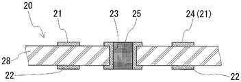
A circuit structure according to embodiment 1 will be described with reference to fig. 1 to 6. As shown in fig. 1 to 3, the circuit structure 1 according to embodiment 1 includes a plate-shaped bus bar 10 and a circuit board 20, and the circuit board 20 is integrated with the bus bar 10. As shown in fig. 2 and 3, one of the features of the circuit structure 1 according to embodiment 1 is that an adhesive sheet 40 is provided between the bus bar 10 and the circuit board 20, and the bus bar 10 and the circuit board 20 are bonded to each other by the adhesive sheet 40. As shown in fig. 3, the present invention is characterized by comprising: a hole-filling resin 25 filled in the via hole 23 provided in the circuit board 20; and a solder resist layer 26 formed on at least the surface of the circuit board 20 facing the bus bar 10 so as to cover the via hole 23 filled with the via filling resin 25. The structure of the circuit structure 1 will be described in detail below. In the following description, the circuit board 20 side of the circuit structure 1 is referred to as the upper side, and the bus bar 10 side is referred to as the lower side.
(bus bar)
The bus bar 10 is a plate-like member constituting a power circuit. In this example, as shown in fig. 2, the bus bar 10 is composed of a plurality of bus bar pieces 11 to 13, and the bus bar pieces 11 to 13 are arranged in a predetermined layout on the same plane. The bus bar 10 (bus bar pieces 11 to 13) is formed of a conductive metal plate, specifically, a plate material made of copper is cut into a predetermined shape. The bus bar 10 (bus bar pieces 11 to 13) has a size suitable for the amount of electricity to be supplied and the amount of heat to be dissipated, and its thickness is, for example, about 0.5mm to 1.0 mm. As described later, the wire harness 90 (see fig. 7) is electrically connected to the bus bar 10. In this example, the bus bar pieces 11 and 12 are respectively formed with terminal insertion holes 15 through which power supply terminals 85 (see fig. 7 and 8) described later are inserted, and the bus bar pieces 11 and 12 are electrically connected to the wire harness 90 via the power supply terminals 85.
(Circuit Board)
As shown in fig. 1 to 3, the circuit board 20 is disposed on the bus bar 10, and includes a control circuit that controls energization of the power circuit. As shown in fig. 3, the circuit board 20 is a double-sided board (multilayer board) having circuit patterns 21 and 22 formed on both sides thereof, and is provided with via holes 23 for electrically connecting the circuit patterns 21 and 22 to each other. Specifically, the circuit board 20 is a printed board in which the circuit patterns 21 and 22 are printed on the insulating substrate 28, and the circuit patterns 21 and 22 are formed of copper foil. The circuit patterns 21 and 22 are covered with solder resist layers 26 and 27, respectively, which will be described later. The circuit board 20 is connected to an external electronic control unit (not shown).
As shown in fig. 1, electronic components such as a part of the terminals of the FET31, a microcomputer (microcomputer) 32, and a control connector 33 are mounted on the circuit board 20 by soldering. The microcomputer 32 is a control element that controls the FET31 and the like. The control connector 33 is a connector to which an electronic control unit is connected, and the electronic components are driven based on a control signal from the electronic control unit. As shown in fig. 3, the circuit pattern 21 on the upper surface of the circuit board 20 is provided with pads 24 for bonding elements (not shown in fig. 3) by solder. The control circuit is constituted by circuit patterns 21, 22 formed on the circuit board 20 and electronic components mounted on the circuit board 20.
In this example, since the other part of the terminals of the FET31 is directly soldered to the bus bar 10, as shown in fig. 2, the element opening 29 corresponding to the FET31 is formed in the portion of the circuit board 20 where the FET31 is disposed.
(pore-filling resin)
As shown in fig. 3, via hole 23 of circuit board 20 is filled with filling resin 25. As described later, the via hole 23 is filled with the hole filling resin 25 when the circuit board 20 is manufactured (see fig. 5). The pore-filling resin 25 is an insulating resin, in this example, an epoxy resin. The hole-filling resin 25 is filled to be coplanar with the upper and lower openings of the via hole 23.
(solder resist layer)
As shown in fig. 3, a solder resist layer 26 is formed on the lower surface (the surface facing the bus bar 10) of the circuit board 20 so as to cover the via hole 23 filled with the via filling resin 25. In this example, the solder resist layer 27 is also formed on the upper surface of the circuit board 20, and the solder resist layer 27 does not cover the portion of the land 24. The solder resist layers 26 and 27 protect the circuit patterns 21 and 22, maintain electrical insulation, and prevent solder from adhering to unnecessary portions when mounting electronic components. As described later, the solder resist layers 26 and 27 are formed by filling the via-filling resin 25 into the via-holes 23 and then applying solder resist ink thereto when the circuit board 20 is manufactured (see fig. 6). Solder resist layers 26 and 27 are made of an insulating resin, in this example, an epoxy resin.
The thickness of the solder resist layer 26 is preferably 5 μm or more, and more preferably 25 μm or more, for example, from the viewpoint of ensuring electrical insulation between the bus bar 10 and the circuit board 20 (circuit pattern 22). The upper limit of the thickness of solder resist layer 26 is, for example, 65 μm from the viewpoint of adhesion to circuit board 20 and workability. The insulation resistance of the solder resist layer 26 is, for example, 500M Ω or more.
(adhesive sheet)
As shown in fig. 2 and 3, the adhesive sheet 40 is interposed between the bus bar 10 and the circuit board 20 (solder resist layer 26), and fixes the circuit board 20 to the bus bar 10. As shown in fig. 3, the adhesive sheet 40 includes a base 41 made of an insulating material, and adhesive layers 42 having adhesiveness at normal temperature are provided on both surfaces of the base 41.
Substrate
The base material 41 of the adhesive sheet 40 is made of a material having heat resistance and electrical insulation properties at a reflow temperature (for example, 260 ℃), and examples thereof include a nonwoven fabric containing cellulose fibers, resin fibers, or glass fibers, and a resin film such as polyimide or polyamideimide. Examples of the resin fibers include polyimide fibers and polyamideimide fibers. Among these, a cellulose nonwoven fabric formed by forming cellulose fibers into a sheet shape is practically useful because it has heat resistance against a reflow temperature and is inexpensive. In this example, the substrate 41 is a nonwoven fabric made of cellulose. The thickness of the base material 41 may be appropriately selected so as to ensure electrical insulation between the bus bar 10 and the circuit board 20, and the thickness of the adhesive sheet 40 including the adhesive layer 42 may be 50 μm or more, for example.
The adhesive layer 42 of the adhesive sheet 40 is formed of an adhesive having heat resistance and electrical insulation properties at a reflow temperature and having adhesiveness at normal temperature, and examples of the adhesive include acrylic adhesives, silicon adhesives, and urethane adhesives. Among them, acrylic adhesives containing acrylic polymers are practical because they have high adhesion, can be stored at room temperature and have excellent storage stability, and are inexpensive. In this example, the adhesive layer 42 is composed of an acrylic adhesive. The adhesive layer 42 is formed by applying an adhesive to both surfaces of the base material 41.
In this example, as shown in fig. 2, an element opening 49 corresponding to the FET31 is formed in the adhesive sheet 40 at the same position as the element opening 29 of the circuit board 20.
< method for manufacturing circuit structure >
An example of a manufacturing procedure of the circuit structure 1 according to embodiment 1 shown in fig. 1 will be described with reference to fig. 2 to 6.
(1) The bus bar 10, the circuit board 20, and the adhesive sheet 40 are prepared (see fig. 2). The bus bar 10 is made by cutting a plate material free of oxygen copper into a prescribed shape. Specifically, a plate material free of oxygen copper is pressed to form a bus bar 10 in which bus bar pieces 11 to 13 having a predetermined shape are arranged as shown in fig. 2.
The circuit board 20 is manufactured as follows. A substrate material is prepared in which a device opening 29 (see fig. 2) and the like are formed in a copper-clad laminate obtained by laminating copper foils on both surfaces of an insulating substrate 28 (see fig. 3) and processed into a predetermined shape. Then, as shown in fig. 4, circuit patterns 21 and 22 and via holes 23 are formed on the substrate material. Specifically, a through hole is bored at a predetermined position of a substrate material by a drill, copper plating is performed on the inner surface of the through hole to form a via hole 23 for electrically connecting the copper foils on both sides, and the copper foils on both sides are etched to form circuit patterns 21 and 22.
Next, as shown in fig. 5, the conductive through hole 23 is filled with an epoxy resin and cured to form a hole-filling resin 25. Then, as shown in fig. 6, solder resist ink of epoxy resin is applied to both surfaces of the circuit board 20 so as to cover the via holes 23, thereby forming solder resist layers 26 and 27. In forming the solder resist layer 27, the solder resist layer 27 is prevented from being formed by masking or the like of a portion of the pad 24 or the like not covered with the solder resist layer 27. The circuit board 20 is manufactured as described above.
The adhesive sheet 40 is produced by cutting an adhesive sheet provided with adhesive layers 42 (see fig. 3) made of an acrylic adhesive on both surfaces of a base material 41 (see fig. 3) of a cellulose nonwoven fabric into a predetermined shape as shown in fig. 2.
(2) The bus bar 10 and the circuit board 20 are bonded to each other by the adhesive sheet 40, and the circuit board 20 is fixed to the bus bar 10 (see fig. 2). Specifically, the bus bar 10 and the circuit board 20 are laminated with the adhesive sheet 40 interposed therebetween, and the bus bar 10 and the circuit board 20 are bonded. Thereby, the bus bar 10 is integrated with the circuit board 20.
(3) After the bus bar 10 is integrated with the circuit board 20, the electronic component is mounted on the circuit board 20 (see fig. 2). Specifically, a solder paste is printed at a position of the circuit board 20 where an electronic component (FET31, etc.) is mounted, the electronic component is mounted, and then the electronic component is placed in a reflow furnace, and the electronic component is soldered to the circuit board 20. In this example, since electronic components are also mounted on the bus bar 10, solder paste is also printed on the bus bar 10. Through the above steps, the circuit structure 1 shown in fig. 1 is obtained.
< action and Effect of Circuit Structure >
The circuit structure 1 of embodiment 1 achieves the following effects.
(1) As shown in fig. 3, in the circuit structure 1, the bus bar 10 is bonded to the circuit board 20 by the adhesive sheet 40 having the adhesive layer 42 having adhesiveness at normal temperature on both surfaces of the base material 41. Therefore, the bus bar 10 and the circuit board 20 can be bonded at normal temperature without performing thermocompression bonding as in the conventional case. Thus, the circuit structure 1 can save the time required for manufacturing by omitting the thermocompression bonding, and can improve the productivity and simplify the manufacturing equipment because the equipment such as the thermocompression bonding device is not required, and the cost is low and the productivity is excellent, as compared with the conventional one. Further, the deformation of the circuit board 20 and the generation of solder cracks due to residual stress caused by thermocompression bonding can be prevented, and the reliability can be improved.
(2) As shown in fig. 3, in the circuit structure 1, the via hole 23 provided in the circuit board 20 is filled with a filling resin 25, and a solder resist layer 26 is formed on the surface of the circuit board 20 facing the bus bar 10. Therefore, by filling the via hole 23 with the hole resin 25, the solder resist layer 26 can be formed so as to cover the via hole 23. On the other hand, when the via hole 23 is not filled with the hole-filling resin 25, the solder resist layer 26 may not be formed in the portion of the via hole 23. Thus, in the circuit structure 1, by forming the solder resist layer 26 so as to cover the via hole 23 filled with the via filling resin 25, the dielectric breakdown voltage between the bus bar 10 and the circuit board 20 is increased as compared with the case where the via filling resin 25 is not filled. This provides high electrical reliability between the bus bar 10 and the circuit board 20, and ensures electrical insulation.
(3) By making the adhesive layer 42 of the adhesive sheet 40 of an acrylic adhesive, the circuit board 20 can be firmly fixed to the bus bar 10. The acrylic adhesive has high adhesiveness and heat resistance, can be stored at room temperature and has excellent storage stability, and is inexpensive, so that the productivity can be improved and the production cost can be reduced.
(4) By using a cellulose nonwoven fabric as the base material 41 of the adhesive sheet 40, the cost of the adhesive sheet 40 can be reduced, and the manufacturing cost can be reduced. For example, the adhesive sheet used in the conventional circuit structure has a polyimide film as a base material and is expensive, whereas a cellulose nonwoven fabric is inexpensive. Thus, by using the adhesive sheet in which the base material is formed of a cellulose nonwoven fabric, the member cost can be reduced as compared with the case of using a conventional adhesive sheet.
< Electrical junction box >
Next, referring to fig. 7 and 8, an electrical junction box 100 according to embodiment 1 will be described. As shown in fig. 8, the electrical junction box 100 according to embodiment 1 includes a circuit structure 1, a heat sink 60, and a case 80. Fig. 7 is a view seen from the lower side of the electrical junction box 100, upside down from fig. 8. The structure of the electrical junction box 100 will be described in detail below. However, the circuit structure 1 shown in fig. 8 is the same as the circuit structure 1 of embodiment 1 shown in fig. 1, and the same objects are denoted by the same reference numerals and their description is omitted.
The heat sink 60 is mounted on the bus bar 10 of the circuit structure 1. The heat sink 60 is made of a high thermal conductive metal material such as aluminum or copper, and in this example, the heat sink 60 is an aluminum plate. The shape of the heat sink 60 is not particularly limited, and may be, for example, a block shape, in addition to a plate shape. The heat sink 60 mainly prevents the temperature of the electronic component (FET31, etc.) mounted on the circuit structure 1 and the temperature of the solder for mounting the electronic component from exceeding allowable temperatures. The size of the heat sink 60 is set to a size suitable for heat dissipation.
The heat sink 60 is attached to the circuit structure 1 (bus bar 10) by, for example, an adhesive sheet having the same structure as the adhesive sheet 40 (see fig. 3) used for the circuit structure 1. The heat sink 60 may be bonded to the circuit structure 1 (bus bar 10) by using an adhesive or an adhesive sheet having an adhesive applied to both surfaces of a base material. When the adhesive sheet is used, since thermocompression bonding is not required, the adhesive sheet can be produced at low cost and is excellent in productivity.
The case 80 houses the circuit structure 1 and the heat sink 60. In this example, as shown in fig. 8, the casing 80 is composed of an upper casing 81 and a lower casing 82. A rod-shaped power supply terminal 85 extending toward the lower case 82 is provided inside the upper case 81. The power supply terminal 85 is inserted into the terminal insertion hole 15 formed in the bus bar 10 (bus bar pieces 11 and 12) of the circuit structure 1 and electrically connected to the bus bar 10. As shown in fig. 7, the power supply terminal 85 protrudes outside the case 80 through a through hole formed in the lower case 82, and a harness 90 is attached to an end portion of the power supply terminal 85 protruding outside from the case 80. Thereby, the bus bar 10 is electrically connected to the wire harness 90 via the power supply terminal 85. In addition, a connector opening 83 is formed in the case 80 so that the control connector 33 of the circuit structure 1 is exposed to the outside of the case 80.
Method for producing electrical junction box
An example of a manufacturing procedure of the electrical junction box 100 according to embodiment 1 shown in fig. 7 will be described with reference to fig. 8.
After the heat sink 60 is attached to the lower surface of the bus bar 10 of the circuit structure 1, the circuit structure 1 is fixed and mounted inside the lower case 82 with screws. Then, the case 80 is assembled by fitting the upper case 81 into the lower case 82. In the above, the electrical junction box 100 shown in fig. 7 is obtained.
[ test examples ]
Sample 2 was produced in the same manner as sample 1, except that the via hole of the circuit board was not filled with the hole-filling resin of the epoxy resin.
Sample 3 used an adhesive sheet in which an epoxy adhesive was applied to both surfaces of a polyimide film substrate, instead of the adhesive sheet of sample 1. The bus bar is bonded to the circuit board by thermocompression bonding the circuit board with the adhesive sheet interposed therebetween. In the circuit structure of sample 3, the via hole of the circuit board was not filled with the hole-filling resin of the epoxy resin, as in sample 2. The thickness of the substrate of the adhesive sheet was 25 μm.
For the circuit structures of samples 1 to 3, a withstand voltage test was performed in which a direct current voltage of 0.8kV to 2.0kV was applied between the circuit board and the bus bar, and electrical insulation was evaluated. In the evaluation, a case where no dielectric breakdown occurred was designated as a, and a case where dielectric breakdown occurred was designated as B. The results are shown in table 1.
[ Table 1]

From the results shown in table 1, the circuit structure of sample 1 did not cause dielectric breakdown until 2.0kV, and had high electrical insulation properties of DC2kV or more. In contrast, the circuit structure of sample 2 exhibited dielectric breakdown at 1.8kV, and the dielectric breakdown voltage was lower than that of sample 1, resulting in a decrease in electrical insulation. In this regard, it is considered that in sample 1, the via hole is filled with the hole resin and the solder resist layer is formed so as to cover the via hole filled with the hole resin, whereby the solder resist layer and the adhesive sheet sufficiently ensure the electrical insulation.
The circuit structure of sample 3 did not cause dielectric breakdown up to 2.0kV, and had high electrical insulation as in sample 1. However, sample 3 requires thermal compression bonding in order, and therefore the operation is more complicated than sample 1, and the productivity is inferior. In addition, in sample 3, the adhesive sheet was expensive because the base material of the adhesive sheet used an expensive polyimide film. In contrast, in sample 1, the base material of the adhesive sheet was a cellulose nonwoven fabric, and the adhesive sheet was lower in cost than the adhesive sheet, and thus the member cost was successfully reduced.
[ use of Circuit Structure and Electrical junction Box ]
The circuit structure and the electrical junction box according to the embodiments of the present invention can be suitably used for an automotive electrical junction box.
Description of the reference symbols
1 Circuit structure
100 electric junction box
10 bus bar
11-13 bus bar sheet
15 terminal insertion hole
20 Circuit board
21. 22 circuit pattern
23 conducting hole
24 bonding pad
25 pore-filling resin
26. 27 solder resist layer
28 insulating substrate
29 opening for element
31 FET
32 micro-computer
33 control connector
40 adhesive sheet
41 base material
42 adhesive layer
49 opening for element
60 radiator
80 case body
81 upper box
82 lower box
83 opening for connector
85 power supply terminal
90 wire harness
Claims (4)
1. A circuit structure is formed by integrating a circuit board having a control circuit for controlling the energization of a power circuit on a plate-like bus bar constituting the power circuit,
wherein the circuit structure includes:
a circuit board having circuit patterns formed on both surfaces thereof and having via holes for electrically connecting the circuit patterns to each other;
an adhesive sheet interposed between the bus bar and the circuit board to fix the circuit board to the bus bar without thermocompression bonding;
filling hole resin filled in the via hole; and
a solder resist layer formed on at least a surface of the circuit board facing the bus bar so as to cover the via hole filled with the via filling resin,
the adhesive sheet comprises a base material made of an insulating material and adhesive layers having adhesiveness at normal temperature on both surfaces of the base material,
the thickness of the solder resist layer is 5 [ mu ] m or more and 65 [ mu ] m or less.
2. The circuit structure body according to claim 1,
the adhesive layer is composed of an acrylic adhesive.
3. The circuit structure body according to claim 1 or 2,
the base material is a nonwoven fabric made of cellulose.
4. An electrical junction box is provided with:
the circuit structure according to any one of claims 1 to 3;
a heat sink mounted to the bus bar; and
and a case for accommodating the circuit structure and the heat sink.
Applications Claiming Priority (3)
| Application Number | Priority Date | Filing Date | Title |
|---|---|---|---|
| JP2015-244888 | 2015-12-16 | ||
| JP2015244888A JP6443688B2 (en) | 2015-12-16 | 2015-12-16 | Circuit structure and electrical junction box |
| PCT/JP2016/086460 WO2017104517A1 (en) | 2015-12-16 | 2016-12-07 | Circuit structure, and electrical connection box |
Publications (2)
| Publication Number | Publication Date |
|---|---|
| CN108432073A CN108432073A (en) | 2018-08-21 |
| CN108432073B true CN108432073B (en) | 2021-07-06 |
Family
ID=59056379
Family Applications (1)
| Application Number | Title | Priority Date | Filing Date |
|---|---|---|---|
| CN201680074201.3A Active CN108432073B (en) | 2015-12-16 | 2016-12-07 | Circuit structure and electrical junction box |
Country Status (5)
| Country | Link |
|---|---|
| US (1) | US20180370463A1 (en) |
| JP (1) | JP6443688B2 (en) |
| CN (1) | CN108432073B (en) |
| DE (1) | DE112016005766B4 (en) |
| WO (1) | WO2017104517A1 (en) |
Families Citing this family (8)
| Publication number | Priority date | Publication date | Assignee | Title |
|---|---|---|---|---|
| JP6548146B2 (en) * | 2016-05-17 | 2019-07-24 | 株式会社オートネットワーク技術研究所 | Circuit structure |
| JP6499124B2 (en) * | 2016-06-30 | 2019-04-10 | 矢崎総業株式会社 | Conductive member and electrical junction box |
| KR101989859B1 (en) * | 2016-12-15 | 2019-09-30 | 주식회사 아모그린텍 | Power relay assembly |
| WO2018173282A1 (en) * | 2017-03-24 | 2018-09-27 | 矢崎総業株式会社 | Electrical junction box and wiring harness |
| JP7001960B2 (en) * | 2018-03-23 | 2022-01-20 | 株式会社オートネットワーク技術研究所 | Circuit configuration |
| DE102019207520A1 (en) * | 2018-06-28 | 2020-01-02 | Robert Bosch Engineering And Business Solutions Private Limited | ELECTRONIC CONTROL UNIT (ECU) TYPE OF A DIRECT CONTACT SYSTEM (DCS) |
| JP6958515B2 (en) * | 2018-09-03 | 2021-11-02 | 株式会社オートネットワーク技術研究所 | Circuit structure and electrical junction box |
| CN111343553B (en) * | 2020-04-09 | 2021-02-19 | 江苏普诺威电子股份有限公司 | MEMS microphone cavity plate with high alignment precision and manufacturing method thereof |
Family Cites Families (16)
| Publication number | Priority date | Publication date | Assignee | Title |
|---|---|---|---|---|
| US5055967A (en) * | 1988-10-26 | 1991-10-08 | Texas Instruments Incorporated | Substrate for an electrical circuit system and a circuit system using that substrate |
| EP1980886A3 (en) * | 2002-04-01 | 2008-11-12 | Ibiden Co., Ltd. | Optical communication device and optical communication device manufacturing method |
| JP2004328939A (en) * | 2003-04-25 | 2004-11-18 | Sumitomo Wiring Syst Ltd | Electrical junction box |
| JP2005117719A (en) * | 2003-10-03 | 2005-04-28 | Auto Network Gijutsu Kenkyusho:Kk | Adhesive sheet for manufacturing circuit structure and manufacturing method of circuit structure using adhesive sheet |
| JP2005294741A (en) * | 2004-04-05 | 2005-10-20 | Auto Network Gijutsu Kenkyusho:Kk | Electric junction box |
| JP2006005107A (en) * | 2004-06-16 | 2006-01-05 | Auto Network Gijutsu Kenkyusho:Kk | Circuit structure body |
| JP2006211776A (en) * | 2005-01-26 | 2006-08-10 | Sumitomo Wiring Syst Ltd | Electrical junction box |
| US7713070B2 (en) * | 2005-04-11 | 2010-05-11 | Autonetwork Technologies, Ltd. | Electric connection box |
| JP2007049036A (en) * | 2005-08-11 | 2007-02-22 | Nitto Denko Corp | Wiring circuit board |
| JP4608422B2 (en) * | 2005-12-05 | 2011-01-12 | 共同技研化学株式会社 | Adhesive film |
| JP5448409B2 (en) * | 2008-10-16 | 2014-03-19 | 日東電工株式会社 | Adhesive composition and adhesive sheet |
| JP5542360B2 (en) * | 2009-03-30 | 2014-07-09 | 太陽ホールディングス株式会社 | Printed wiring board |
| DE102009053998A1 (en) | 2009-11-19 | 2011-05-26 | Still Gmbh | Inverter, in particular multi-phase three-phase converter |
| JP5901923B2 (en) * | 2011-09-30 | 2016-04-13 | 太陽インキ製造株式会社 | Thermosetting resin filler and printed wiring board |
| DE102013219192A1 (en) | 2013-09-24 | 2015-03-26 | Conti Temic Microelectronic Gmbh | Power module, power converter and drive arrangement with a power module |
| JP6136946B2 (en) * | 2014-01-22 | 2017-05-31 | 株式会社オートネットワーク技術研究所 | Switching board |
-
2015
- 2015-12-16 JP JP2015244888A patent/JP6443688B2/en active Active
-
2016
- 2016-12-07 US US15/775,952 patent/US20180370463A1/en not_active Abandoned
- 2016-12-07 CN CN201680074201.3A patent/CN108432073B/en active Active
- 2016-12-07 WO PCT/JP2016/086460 patent/WO2017104517A1/en active Application Filing
- 2016-12-07 DE DE112016005766.0T patent/DE112016005766B4/en active Active
Also Published As
| Publication number | Publication date |
|---|---|
| DE112016005766B4 (en) | 2022-06-09 |
| JP2017112708A (en) | 2017-06-22 |
| JP6443688B2 (en) | 2018-12-26 |
| CN108432073A (en) | 2018-08-21 |
| WO2017104517A1 (en) | 2017-06-22 |
| US20180370463A1 (en) | 2018-12-27 |
| DE112016005766T5 (en) | 2018-08-30 |
Similar Documents
| Publication | Publication Date | Title |
|---|---|---|
| CN108432073B (en) | Circuit structure and electrical junction box | |
| US20070010086A1 (en) | Circuit board with a through hole wire and manufacturing method thereof | |
| US7903417B2 (en) | Electrical circuit assembly for high-power electronics | |
| CN108370142B (en) | Circuit structure and electrical junction box | |
| KR20150104033A (en) | Ultra-thin embedded semiconductor device package and method of manufacturing therof | |
| US10164417B2 (en) | Circuit assembly and electrical junction box | |
| US8289728B2 (en) | Interconnect board, printed circuit board unit, and method | |
| JP2018506855A (en) | Electronic component and method for manufacturing such an electronic component | |
| US20110085314A1 (en) | Electrical circuit system and method for producing an electrical circuit system | |
| JP2008021819A (en) | Heat conducting base board, manufacturing method thereof, power supply unit, and electronic equipment | |
| EP2273858A1 (en) | Printed circuit board unit and electronic device | |
| US20110174526A1 (en) | Circuit module | |
| CN109429431A (en) | Circuit substrate | |
| US7688591B2 (en) | Electronic-component-mounting board | |
| CN109698172B (en) | Circuit structure and method for manufacturing circuit structure | |
| KR101115403B1 (en) | Light emitting apparatus | |
| JP2003218317A (en) | Semiconductor power conversion device | |
| CN106170174B (en) | Printed circuit board and electronic device | |
| JP2019140321A (en) | Electronic component mounting substrate and electronic device | |
| JP2016076509A (en) | Circuit module | |
| US20080084671A1 (en) | Electrical circuit assembly for high-power electronics | |
| JP2004259904A (en) | Circuit board of electronic circuit device and method of manufacturing the same | |
| Lee et al. | Coin insertion technology for PCB thermal solution | |
| JPH05327156A (en) | Printed-circuit board | |
| JP6403741B2 (en) | Surface mount semiconductor package equipment |
Legal Events
| Date | Code | Title | Description |
|---|---|---|---|
| PB01 | Publication | ||
| PB01 | Publication | ||
| SE01 | Entry into force of request for substantive examination | ||
| SE01 | Entry into force of request for substantive examination | ||
| GR01 | Patent grant | ||
| GR01 | Patent grant |