WO2017104398A1 - 生体分子測定装置 - Google Patents
生体分子測定装置 Download PDFInfo
- Publication number
- WO2017104398A1 WO2017104398A1 PCT/JP2016/085321 JP2016085321W WO2017104398A1 WO 2017104398 A1 WO2017104398 A1 WO 2017104398A1 JP 2016085321 W JP2016085321 W JP 2016085321W WO 2017104398 A1 WO2017104398 A1 WO 2017104398A1
- Authority
- WO
- WIPO (PCT)
- Prior art keywords
- fixing member
- biomolecule
- nanopore
- liquid tank
- groove structure
- Prior art date
- Legal status (The legal status is an assumption and is not a legal conclusion. Google has not performed a legal analysis and makes no representation as to the accuracy of the status listed.)
- Ceased
Links
Images



































Classifications
-
- G—PHYSICS
- G01—MEASURING; TESTING
- G01N—INVESTIGATING OR ANALYSING MATERIALS BY DETERMINING THEIR CHEMICAL OR PHYSICAL PROPERTIES
- G01N33/00—Investigating or analysing materials by specific methods not covered by groups G01N1/00 - G01N31/00
- G01N33/48—Biological material, e.g. blood, urine; Haemocytometers
- G01N33/483—Physical analysis of biological material
- G01N33/487—Physical analysis of biological material of liquid biological material
- G01N33/48707—Physical analysis of biological material of liquid biological material by electrical means
- G01N33/48721—Investigating individual macromolecules, e.g. by translocation through nanopores
-
- C—CHEMISTRY; METALLURGY
- C12—BIOCHEMISTRY; BEER; SPIRITS; WINE; VINEGAR; MICROBIOLOGY; ENZYMOLOGY; MUTATION OR GENETIC ENGINEERING
- C12M—APPARATUS FOR ENZYMOLOGY OR MICROBIOLOGY; APPARATUS FOR CULTURING MICROORGANISMS FOR PRODUCING BIOMASS, FOR GROWING CELLS OR FOR OBTAINING FERMENTATION OR METABOLIC PRODUCTS, i.e. BIOREACTORS OR FERMENTERS
- C12M1/00—Apparatus for enzymology or microbiology
-
- C—CHEMISTRY; METALLURGY
- C12—BIOCHEMISTRY; BEER; SPIRITS; WINE; VINEGAR; MICROBIOLOGY; ENZYMOLOGY; MUTATION OR GENETIC ENGINEERING
- C12N—MICROORGANISMS OR ENZYMES; COMPOSITIONS THEREOF; PROPAGATING, PRESERVING, OR MAINTAINING MICROORGANISMS; MUTATION OR GENETIC ENGINEERING; CULTURE MEDIA
- C12N15/00—Mutation or genetic engineering; DNA or RNA concerning genetic engineering, vectors, e.g. plasmids, or their isolation, preparation or purification; Use of hosts therefor
- C12N15/09—Recombinant DNA-technology
-
- G—PHYSICS
- G01—MEASURING; TESTING
- G01N—INVESTIGATING OR ANALYSING MATERIALS BY DETERMINING THEIR CHEMICAL OR PHYSICAL PROPERTIES
- G01N27/00—Investigating or analysing materials by the use of electric, electrochemical, or magnetic means
-
- G—PHYSICS
- G01—MEASURING; TESTING
- G01N—INVESTIGATING OR ANALYSING MATERIALS BY DETERMINING THEIR CHEMICAL OR PHYSICAL PROPERTIES
- G01N27/00—Investigating or analysing materials by the use of electric, electrochemical, or magnetic means
- G01N27/26—Investigating or analysing materials by the use of electric, electrochemical, or magnetic means by investigating electrochemical variables; by using electrolysis or electrophoresis
- G01N27/28—Electrolytic cell components
- G01N27/30—Electrodes, e.g. test electrodes; Half-cells
- G01N27/327—Biochemical electrodes, e.g. electrical or mechanical details for in vitro measurements
- G01N27/3275—Sensing specific biomolecules, e.g. nucleic acid strands, based on an electrode surface reaction
- G01N27/3278—Sensing specific biomolecules, e.g. nucleic acid strands, based on an electrode surface reaction involving nanosized elements, e.g. nanogaps or nanoparticles
-
- G—PHYSICS
- G01—MEASURING; TESTING
- G01N—INVESTIGATING OR ANALYSING MATERIALS BY DETERMINING THEIR CHEMICAL OR PHYSICAL PROPERTIES
- G01N27/00—Investigating or analysing materials by the use of electric, electrochemical, or magnetic means
- G01N27/26—Investigating or analysing materials by the use of electric, electrochemical, or magnetic means by investigating electrochemical variables; by using electrolysis or electrophoresis
- G01N27/403—Cells and electrode assemblies
- G01N27/414—Ion-sensitive or chemical field-effect transistors, i.e. ISFETS or CHEMFETS
- G01N27/4145—Ion-sensitive or chemical field-effect transistors, i.e. ISFETS or CHEMFETS specially adapted for biomolecules, e.g. gate electrode with immobilised receptors
-
- B—PERFORMING OPERATIONS; TRANSPORTING
- B01—PHYSICAL OR CHEMICAL PROCESSES OR APPARATUS IN GENERAL
- B01L—CHEMICAL OR PHYSICAL LABORATORY APPARATUS FOR GENERAL USE
- B01L3/00—Containers or dishes for laboratory use, e.g. laboratory glassware; Droppers
- B01L3/50—Containers for the purpose of retaining a material to be analysed, e.g. test tubes
- B01L3/502—Containers for the purpose of retaining a material to be analysed, e.g. test tubes with fluid transport, e.g. in multi-compartment structures
- B01L3/5027—Containers for the purpose of retaining a material to be analysed, e.g. test tubes with fluid transport, e.g. in multi-compartment structures by integrated microfluidic structures, i.e. dimensions of channels and chambers are such that surface tension forces are important, e.g. lab-on-a-chip
- B01L3/502715—Containers for the purpose of retaining a material to be analysed, e.g. test tubes with fluid transport, e.g. in multi-compartment structures by integrated microfluidic structures, i.e. dimensions of channels and chambers are such that surface tension forces are important, e.g. lab-on-a-chip characterised by interfacing components, e.g. fluidic, electrical, optical or mechanical interfaces
Definitions
- the present invention relates to a biomolecule measuring apparatus using nanopores.
- next-generation DNA sequencer As a next-generation DNA sequencer, a method for electrically directly measuring DNA base sequence without performing an extension reaction and a fluorescent label has been attracting attention.
- a nanopore DNA sequencing method in which a DNA fragment is directly measured and a base sequence is determined without using a reagent has been actively promoted.
- This method is based on the principle of sequentially identifying the base species by directly measuring the difference between the individual base species contained in the DNA strand with the amount of blocking current when the DNA strand passes through the nanopore. Since the template DNA is not amplified by an enzyme and a label such as a phosphor is not used, this method is expected to lead to high throughput, low running cost, and long base length decoding.
- One of the problems with the nanopore method is the control of DNA transport through the nanopore.
- the nanopore passage speed of DNA In order to measure the difference between individual base species contained in DNA strands by the amount of blocking current, it is necessary to set the nanopore passage speed of DNA to 100 ⁇ s or more per base from the current noise during measurement and the time constant of DNA molecule fluctuation. There are thought to be.
- sequencing DNA using a nanopore a potential gradient is formed using electrodes positioned above and below the nanopore, and DNA having a negative charge is passed through the nanopore.
- the nanopore passage speed of DNA is usually as fast as 1 ⁇ s or less per base, and it is difficult to sufficiently measure the blocking current derived from each base.
- the DNA end to be read is fixed to the tip of the fixed probe, and the movement of DNA passing through the nanopore is controlled by controlling the minute displacement of the fixed probe with an external drive mechanism (motor and piezo element). There is something to control.
- the signal measured by the biomolecule measuring apparatus using the nanopore device is a rectangular staircase signal indicating a different level depending on the monomer molecular species constituting the biomolecule. Furthermore, the signal response speed of the biomolecule measuring apparatus, the solution resistance of the electrolyte solution filled in the peripheral nanopore device and (R L), the nanopore device capacity and (C s), the approach of the nanopore device with fixed probe It is defined by the passage resistance (R g ) defined by the size of the narrow region that accompanies it.
- the nanopore device and the fixed probe are brought close to each other when analyzing the biomolecule.
- the distance between the nanopore device and the fixed probe decreases, leading to an increase in passage resistance. This means a decrease in the signal time constant, resulting in a rounded signal waveform and a decrease in SN.
- the present invention provides a technique for reducing the passage resistance of a solution and suppressing a decrease in time constant.
- the present invention proposes a technique for forming a groove structure in at least one of a fixing member (fixed probe) and a nanopore device in a biomolecule measuring device to suppress an increase in passage resistance.
- the present application includes a plurality of means for solving the above-described problems.
- a first liquid tank filled with an electrolyte solution a second liquid tank filled with an electrolyte solution, and a thin film having nanopores
- a nanopore device provided between the first liquid tank and the second liquid tank so as to communicate the first liquid tank and the second liquid tank via the nanopore
- a fixing member disposed in the first liquid tank and having a size larger than that of the thin film, to which a biomolecule is fixed; and a driving mechanism for driving the fixing member in a direction approaching or moving away from the thin film
- a first electrode provided in the first liquid tank a second electrode provided in the second liquid tank; a stop mechanism for preventing contact between the fixing member and the thin film
- a voltage is applied between one electrode and the second electrode
- a measurement unit that measures an ionic current flowing between the first electrode and the second electrode, and at least one of the nanopore device and the fixing member is opposed to the
- a first liquid tank filled with an electrolyte solution, a second liquid tank filled with an electrolyte solution, and a thin film having nanopores are supported, and the first pores are interposed via the nanopores.
- a nanopore device provided between the first liquid tank and the second liquid tank so as to communicate the liquid tank and the second liquid tank; and a first provided in the first liquid tank.
- An electrode a second electrode provided in the second liquid tank, a power source for applying a voltage between the first electrode and the second electrode, the first electrode, and the second electrode
- a fixing member for fixing a biomolecule in a biomolecule measuring apparatus wherein the fixing member has a groove structure formed on the surface of the fixing member.
- a nanopore device for a biomolecule measuring apparatus comprising: a thin film having a nanopore; and a space forming member provided outside the thin film and forming a space around the nanopore.
- a nanopore device is provided in which the space forming member comprises a groove structure.
- FIG. 1 It is a cross-sectional schematic diagram explaining the structural example of a biomolecule measuring apparatus. It is explanatory drawing of the equivalent circuit of a nanopore device and a peripheral mechanism. It is a graph which shows the relationship between the distance between a fixing member and a nanopore device, solution resistance, and passage resistance. The signal schematic diagram when a fixing member is brought close to the nanopore device and then the fixing member is separated from the nanopore device is shown. It is a figure explaining the range which forms a groove
- the nanopore described in each example is a nano-sized hole penetrating the front and back provided in the thin film.
- the thin film is mainly formed of an inorganic material. Examples of the thin film material include SiN, SiO 2 , Graphene, Graphite, Si, and the like, but can also include organic substances, polymer materials, and the like.
- the nanopore thin film having nanopores is formed on a part of the nanopore device, and has a structure that does not have a support film on the top and bottom and is supported by the nanopore device and floats in the air.
- Biomolecules referred to in this specification include nucleic acids, proteins, amino acids, long-chain polymers, and the like.
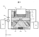
- FIG. 1 is a schematic cross-sectional view illustrating a configuration example of a biomolecule measuring apparatus.
- the biomolecule measuring apparatus 100 of the present embodiment includes two upper and lower liquid tanks 131 and 132 separated by a nanopore device (also referred to as a nanopore substrate) 101.
- the liquid baths 131 and 132 are filled with the electrolyte solution 102.
- the electrolyte solution KCl, NaCl, LiCl, CsCl, MgCl 2 or the like is used.
- a buffering agent can be mixed for the stabilization of biomolecules.
- Tris, EDTA, PBS, or the like is used as the buffer.
- the thin film 113 is formed in the nanopore device 101, and the nanopore 112 is formed at any position in the thin film 113.
- the two upper and lower liquid tanks 131 and 132 communicate with each other through the nanopore 112 of the thin film 113 supported by the nanopore device 101.
- Ag / AgCl electrodes 103a and 103b are respectively arranged in the two liquid tanks 131 and 132 so as to contact the electrolyte solution 102, and a power source 104 and an ammeter 109 are connected between the electrodes 103a and 103b.
- the ammeter 109 is connected to an ADC (not shown) and the PC 110, and the PC 110 can record the acquired current value.
- the drive mechanism 105 is installed in the upper liquid tank 131 and connected to the drive mechanism control unit 106.
- a biomolecule fixing member (hereinafter simply referred to as a fixing member) 107 is connected to the driving mechanism 105 by a connecting member 111.
- the fixing member 107 has a size larger than that of the thin film 113 in plan view, and the biomolecule 108 is fixed to the flat lower surface of the fixing member 107.
- the stop mechanism of the present embodiment is a space forming member 114 that surrounds the periphery of the nanopore device 101 outside the thin film 113 like a bank and forms a space between the fixing member 107 and the thin film 113.
- a thin film 113 having nanopores 112 is arranged in a circular space formed at the center of the space forming member 114, and the dimension of the thin film 113 in plan view is smaller than the dimension of the fixing member 107. Therefore, the fixing member 107 that has moved toward the nanopore device 101 stops against the space forming member 114 before coming into contact with the thin film 113 and does not come into contact with the thin film 113 to be destroyed.
- the dimension of the thin film 113 needs to be an area where it is difficult to form two or more holes when forming a hole by thin film strength and voltage application, so one side (the length of the side if the thin film 113 is a rectangle, If the shape is circular, the length of the diameter may be about 100 to 500 nm. In order to achieve DNA single-base resolution, about 1 nm is appropriate as a film thickness that can form the nanopore 112 having an effective film thickness corresponding to one base.
- the thickness of the space forming member 114 is suitably about 200 to 500 nm in consideration of maintaining the strength of the thin film 113 and fluctuations in the fixing height of the biomolecules on the surface of the fixing member 107. In this embodiment, the thin film 113 has a diameter of 500 nm and the space forming member 114 has a thickness of 250 nm.
- the base species constituting the DNA are identified from the resistance change when the DNA passes through the nanopore 112.
- the signal change acquired at that time is assumed to be rectangular.
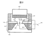
- FIG. 2 shows an equivalent circuit of the nanopore device and its surrounding environment.
- 201 is a pore resistance R p
- 202 is a combined resistance (R L + R g ) of solution resistance and passage resistance
- 203 is a nanopore device capacitance C s .
- R g L / ⁇ Wh It is expressed by
- the time constant of the signal is required to be 10 us or less. That is, when the substrate capacitance Cs is 600 uF, Rg needs to be 100 k ⁇ .
- At least one of the nanopore device 101 and the fixing member 107 includes a groove structure in a range where the nanopore device 101 and the fixing member 107 face each other.
- the groove structure needs to be in contact with the electrolyte solution 102 and is formed in a region in the electrolyte solution where the nanopore device 101 and the fixing member 107 face each other.
- the groove may be formed with a concavo-convex structure or may be formed with a hole structure penetrating the fixing member 107.
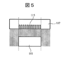
- FIGS. 5 and 6 are diagrams for more specifically explaining the range in which the groove is formed.
- the plurality of grooves 115 may be formed in a range where the nanopore device 101 and the fixing member 107 face each other (a range indicated by a dotted line in FIGS. 5 and 6).
- FIG. 5 is an example in which the plurality of grooves 115 are formed only in the fixing member 107.
- the manufacturing method becomes simpler and the cost can be reduced as compared with the case of forming the groove 115 in the nanopore device 101.
- FIG. 6 is an example in which the plurality of grooves 115 are formed only in the nanopore device 101.
- the peripheral space of the nanopore 112 for example, the space 121 in FIG. 1
- the space in the region where the nanopore device 101 and the fixing member 107 do not face each other for example, the space 122 on the side surface of the fixing member 107 in FIG. 1 needs to be in electrical contact.
- the groove structure does not need to be formed continuously. The following example will be described.
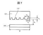
- FIG. 7 shows an example of a configuration in which the fixing member 107 is stopped at a position slightly above the nanopore device 101 when the fixing member 107 descends toward the nanopore device 101.
- FIG. 8 is a plan view of the fixing member 107 in the configuration of FIG.
- the drive mechanism 105 controls the fixing member 107 to stop at a position slightly above the nanopore device 101 (the relative distance between the fixing member 107 and the nanopore device 101 does not become zero).
- the groove 115 does not need to extend so as to reach the edge of the fixing member 107 (FIG. 8). That is, the groove 115 does not have to be continuously formed in the entire range where the nanopore device 101 and the fixing member 107 are opposed to each other. In this case, there may be a region where the groove 115 is not partially formed within a range in which the nanopore device 101 and the fixing member 107 face each other.
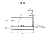
- FIG. 9 shows an example of a configuration in which the fixing member 107 contacts the nanopore device 101 when the fixing member 107 descends toward the nanopore device 101.
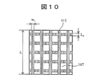
- FIG. 10 is a plan view of the fixing member 107 in the configuration of FIG.
- the fixing member 107 when the driving mechanism 105 lowers the fixing member 107 toward the nanopore device 101, the fixing member 107 completely contacts the nanopore device 101 (between the fixing member 107 and the nanopore device 101. Relative distance is 0).
- the groove 115 extends so as to reach the edge of the fixing member 107 (that is, the end of the range where the nanopore device 101 and the fixing member 107 face each other). (FIG. 10). That is, the groove 115 is continuously formed over the entire range where the nanopore device 101 and the fixing member 107 are opposed to each other.
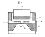
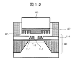
- FIG. 11, FIG. 12, and FIG. 13 show examples of the groove structure.
- the groove structure may be continuously formed in a range where the nanopore device 101 and the fixing member 107 are opposed to each other.
- the plurality of grooves 115 are formed only in the space forming member 114 of the nanopore device 101.
- the groove structure may be formed in both the nanopore device 101 and the fixing member 107.
- the outer peripheral portion of the fixing member 107 includes a plurality of grooves 115
- the peripheral portion of the nanopore 112 in the space forming member 114 of the nanopore device 101 includes the plurality of grooves 115.
- the plurality of grooves 115 are continuously formed between the upper fixing member 107 and the lower nanopore device 101 in a range where the nanopore device 101 and the fixing member 107 face each other. Good.
- the fixing member 107 includes a plurality of grooves 115 in a region around the nanopore 112, and the nanopore device 101 includes a plurality of grooves 115 outside the region.
- FIGS. 16 and 17 are diagrams for explaining the passage resistance R 1 in configuration including a groove structure of the present embodiment.
- R 1 (L ⁇ nL 1 ) / (Wh 0 + w 1 h 1 n)
- FIG. 18 is a graph showing the relationship between the groove depth and the solution resistance when the relationship between the groove width and the groove pitch is changed.
- ⁇ is the ratio of w 1 and w 2
- w 1 ⁇ ⁇ w 2 .
- “Series 4” is a target value of the solution resistance.
- the digging depth of the groove 115 is about 5 [mu] m, it is possible to achieve the target value.
- the digging depth of the groove 115 is preferably 5 ⁇ m or more.
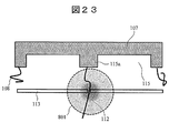
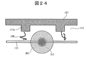
- FIG. 21 is an enlarged view of the vicinity of the nanopore when the fixing member includes a groove.
- a convex portion 115a and a concave portion 115b are formed at a portion where the groove 115 is formed.
- the width of the convex portion 115a needs to have a size equal to or larger than the DNA fixing pitch. It is conceivable that the DNA fixing pitch is at an interval of 100 nm due to its nature. Therefore, for example, it is desirable that the width of the convex portion at the portion where the groove 115 is formed be 100 nm or more.
- the pitch of the grooves 115 (corresponding to w 2 described above) needs to be 300 nm or less.
- 21 and 22 are examples in which the pitch of the grooves 115 is 300 nm or less.
- the pitch of the groove 115 is 300 nm or less.
- the space forming member 114 can be configured in an arbitrary shape. However, the space forming member 114 is not configured as illustrated in FIG. 1, and has the following restrictions when the convex portion is formed on the nanopore device 101 (for example, , Etc. in the case of the space forming member of FIG. In dimensions greater than the width of the space forming member, the case of forming the width of the groove 115 (corresponding to w 1 above), the fixing member 107 when allowed to fully contact the nanopore device 101, made a high resistance region End up. Therefore, it is necessary to avoid complete contact between the fixing member 107 and the nanopore device 101 or limit the width of the groove 115 to be equal to or smaller than the width of the space forming member.
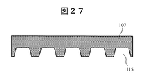
- a fixing member having a groove structure are examples of a fixing member having a groove structure.
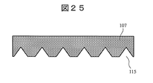
- the cross section of the groove structure is not limited to the rectangle shown in FIG. 1, but may be a triangle, a half moon, or a trapezoid.
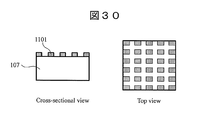
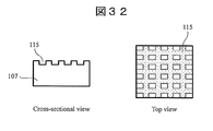
- a method for forming a groove structure in the fixing member 107 will be described with reference to FIGS.
- a silicon substrate 107 serving as a fixing member is prepared (FIG. 28).
- a resist 1101 is applied on the silicon substrate 107 (FIG. 29).
- the resist 1101 is patterned with a desired dimension (FIG. 30).
- the silicon substrate 107 is cut by dry etching to form a groove 115 (FIG. 31).
- the resist 1101 on the silicon substrate 107 is removed (FIG. 32).
- the groove 115 may be formed by processing the silicon substrate 107 with a dicing blade without using a resist or the like.
- the concave portion and the convex portion of the groove structure are formed of the same material.
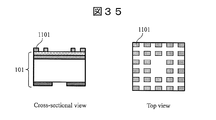
- the formation process of the groove 115 is preferably inserted into the manufacturing process of the nanopore device 101.
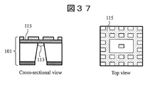
- a silicon substrate 3301 to be a substrate for the nanopore device 101 is prepared (FIG. 33).
- a nitride film, an oxide film, and a nitride film are formed on the silicon substrate 3301, a nitride film is formed on the back surface of the silicon substrate 3301, and a resist 1101 is applied to the uppermost surface of the silicon substrate 3301 after the film formation (FIG. 34).
- the resist 1101 is patterned with a desired dimension (FIG. 35).
- patterning for opening a thin film and patterning for silicon etching are performed. Since the positions of the thin film 113 and the nanopore 112 are specified by the pattern here, patterning for the groove structure is performed on the resist 1101 using the above pattern as a mark.
- a dicing blade may be used to create a groove structure. Etching is performed on the front and back surfaces according to the created pattern (FIG. 36).
- the resist 1101 can be removed, and the groove 115 can be formed on the nanopore device 101 (FIG. 37).
- This example is basically the same as the method described with reference to FIGS. 28 to 32, but differs in that two films are formed before the groove processing is performed.
- a silicon substrate 107 serving as a fixing member is prepared (FIG. 38).
- a first film 1302 to which the biomolecule 108 is difficult to bind is formed on the silicon substrate 107, and then a second film 1301 to which the biomolecule 108 is easily bonded is formed (FIG. 39).
- the second film 1301 is etched (FIG. 40). Note that a gas type is selected so that an etch stop occurs in the first film 1302 during etching.
- a polySi film may be used as the first film.
- gold, nickel, titanium, or the like may be used as the second film.
- APTES can be formed on the Si film and not bonded to the metal part.
- the biomolecule 108 (for example, DNA) can bind to the entire surface of the fixing member 107 described above, but the groove structure material can be selected as described above.
- the material of the groove structure is selected and, for example, that DNA can be immobilized only on the convex portion of the groove 115 (that is, the second film 1301 described above) not only increases the reliability of the signal but also reads the DNA longer. This is also effective in terms of points.
- a material on which the target biomolecule 108 cannot be fixed is formed on the silicon substrate as the first layer, and the material on which the biomolecule 108 can be fixed is used as the second layer.
- a film is formed on the first layer.
- a groove 115 is formed in the second layer.
- etching is performed using gases having different etch rates between the second layer and the first layer.
- a third film may be formed between the first layer and the second layer, and the third film may be used as an etching stop role.
- a silicon nitride layer may be further formed on the Si layer, and then the silicon nitride layer may be patterned to serve as an Si layer etching mask. Further, wet etching with KOH may be performed. In this case, the cross section of the groove is trapezoidal or triangular.
- the biomolecule 108 on the fixing member 107 may be bonded through different biomolecules (for example, APTES, thiol, PNA having an arbitrary sequence) fixed on the fixing member 107 in advance.
- biomolecules for example, APTES, thiol, PNA having an arbitrary sequence
- the groove structure can be used as a means for determining a fixed position address.
- 41 to 44 show an example of a method for fixing a plurality of types of biomolecules on a fixing member.
- the selection marker is fixed to the fixing member 107.
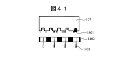
- the marker stock solution 1403 is applied to the fixing member 107 having the grooves 115 by the ink jet method using the mask 1402 (FIG. 41).
- the selection marker 1401 is fixed to the fixing member 107.
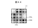
- the marker stock solution 1403 different types of stock solutions are selected for each address (region of the fixing member 107) according to the biomolecule to be fixed.
- FIG. 42 is a plan view of the fixing member after performing the above-described process. As shown in FIG. 44, a plurality of different biomolecules 1404a, 1404b, 1404c can be bound for each address of the fixing member 107.
- Nanopore device fabrication methods and nanopore formation methods are known and are described, for example, in Itaru Yanagi et al., Sci. Rep. 4, 5000 (2014).
- a thin film for forming nanopores was produced by the following procedure. First, the surface 8-inch Si wafer 725 ⁇ m thickness was 112nm deposited Si 3 N 4 and Si 3 N 4 / SiO 2 / Si 3 N 4 12nm / 250nm / 100nm, the rear surface. Next, the surface top the Si 3 N 4 to 500nm square, and 1038 ⁇ m square back surface the Si 3 N 4, and each reactive ion etching.
- the Si substrate exposed by etching on the back surface was etched with TMAH (Tetramethylammonium hydroxide).
- TMAH Tetramethylammonium hydroxide
- the wafer surface was covered with a protective film in order to prevent surface-side SiO etching.
- Formation of nanopores on the thin film exposed to the nanopore device was performed by the following procedure using a pulse voltage.
- the Si 3 N 4 thin film was hydrophilized with Ar / O 2 plasma under the conditions of 10 W, 20 sccm, 20 Pa, 45 sec.
- 1M KCl, 1 mM Tris-10 mM EDTA, pH 7.5 solution is filled, and each tank is filled with Ag / AgCl.
- An electrode was introduced.
- the voltage application for forming the nanopore and the measurement of the ion current flowing through the nanopore after the nanopore is formed are performed between the Ag / AgCl electrodes.
- the lower tank was called the cis tank
- the upper tank was called the trans tank
- the voltage V cis on the cis tank electrode side was set to 0 V
- the voltage V trans on the trans tank electrode side was selected.
- the selected voltage was applied with a pulse generator.
- the current value after application of each pulse was read with a current amplifier.
- the process of voltage application and ion current reading for nanopore formation was controlled by a program.
- the pulse voltage application condition by selecting the current value condition (threshold current) acquired according to the pore diameter formed in the thin film before applying the pulse voltage, the pore diameter is sequentially increased, and the target pore diameter is set. Obtained. The pore diameter was estimated from the ion current value.
- the criteria for condition selection are as shown in Table 1.
- nanopores are possible not only by applying a pulse voltage but also by electron beam irradiation with TEM (A. J. Storm et al., Nat. Mat. 2 (2003)).
- the displacement of the biomolecule 108 is the length of one base, that is, 0.
- the configuration needs not to change by 34 nm or more.
- F is the force applied to the system
- S is the area of the material
- L is the length of the material
- ⁇ L is the amount of displacement when receiving the applied force. It has been found that when 1 mV is applied vertically through a nanopore, the force applied to DNA is 0.24 pN (Ulrich F. Keyser et al., Nat. Phys. 2, 473-477 (2006)). . Since fluctuation of the applied voltage during the analysis can occur about 0.1 mV, it is necessary that the displacement does not exceed 0.34 nm. Accordingly, the Young's modulus of the fixing member 107, the drive mechanism 105, and the connecting member 111 needs to be 0.07 (L / S) [ ⁇ N / mm 2 ] or more.
- the measurement system is thermally stable. Even when there is no heat source, the space is known to have a fluctuation of 0.1 degree. Therefore, the temperature change of the distance between the nanopore device 101 and the fixing member 107 calculated from the entire material used in the system needs to be 0.34 nm or less per 0.1 ° C.
- connection member 111 a screw or the like made of stainless steel or invar may be used as the connection member 111.
- the fixing member 107 may be fixed to the drive mechanism 105 by vacuum suction or pressure bonding.
- the drive mechanism 105 is made of a piezoelectric material typified by a piezo element, and can be driven at 0.1 nm / s or more.
- the piezoelectric material barium titanate (BaTiO 3 ), lead zirconate titanate (PZT), zinc oxide (ZnO), or the like is used.
- the end of the biomolecule 108 and the surface of the fixing member 107 can be bonded to each other by a covalent bond, an ionic bond, an electrostatic interaction, a magnetic force, or the like.
- DNA when DNA is immobilized by a covalent bond, DNA whose end has been modified with APTES or glutaraldehyde can be immobilized.
- Si and SiO serving as a scaffold for APTES are used.
- a gold thiol bond can be used as another covalent bonding method.
- the 5 'end of the DNA is thiol-modified, and the surface of the fixing member 107 is gold-deposited.
- Ag, Pt, and Ti that can bond thiol can be used as the metal species to be deposited on the fixing member 107.
- the method using ionic bonding is a method in which a negatively charged biomolecule is fixed to the surface of the positively charged fixing member 107 by performing a process of positively charging the fixing member 107 in a solution by surface modification.
- a cationic polymer polyaniline or polylysine is used.
- electrostatic interaction is used, the amino-terminal modified DNA can be directly immobilized on the surface of the APTES-modified fixing member 107.
- a nitrocellulose film, a polyvinylidene fluoride film, a nylon film, or a polystyrene substrate is widely used. In particular, nitrocellulose membranes are used in microarray technology.
- DNA is immobilized in advance on the surface of the magnetic beads, for example, using the above-described bonds. Further, by using a magnetic material as the fixing member 107, the magnetic beads having the DNA immobilized thereon interact with the fixing member 107, thereby realizing attraction of the DNA-immobilized magnetic beads by magnetic force.
- a magnetic material iron, silicon steel, amorphous magnetic alloy, nanocrystal magnetic alloy, or the like is used.
- the specific binding site can be modified and bound to the fixing member 107 in the same manner. This makes it possible to specify the binding site in the protein and obtain amino acid sequence information.
- FIG. 19 is a schematic diagram showing an electric field generated around the nanopore and an example of biomolecule introduction into the nanopore.
- the potential gradient 801 spreading around the nanopore 112 has the following relationship among the distance L from the nanopore 112, the nanopore diameter d, the thickness t of the thin film, and the applied voltage ⁇ V.
- the range in which the biomolecule is confined in this electric field and introduced into the nanopore can be obtained. If the range is L diff , it is expressed by the following equation.
- the distance when the fixing member 107 comes closest to the thin film 113 is l.
- the biomolecule fixed pitch a is as follows.
- FIG. 20 is a schematic diagram illustrating an example of introducing an electric field generated around a nanopore and a biomolecule into the nanopore.
- a biomolecule (DNA) 108 is immobilized in a mixture with a short-chain polymer 206 whose end is modified, and a DNA immobilization member having a target DNA immobilization density can be effectively produced.
- a fixing member is prepared using a DNA solution containing 20% of polymer (dA) 75%, the phenomenon of multiple DNAs entering one pore is eliminated using nanopores having a pore diameter of 2.5 to 3 nm. I have confirmed that I can do it. That is, it is considered that the pitch can be fixed at about 100 nm pitch.
- the length of the short chain polymer to be mixed is not necessarily about 2 nm.
- the biomolecule measuring apparatus 100 in which the biomolecule fixing region (planar size of the fixing member 107) is equal to or larger than the planar size of the thin film 113 having the nanopore 112, at least one of the fixing member 107 and the nanopore device 101.
- a groove structure is formed. Thereby, a raise of passage resistance can be controlled. Since the solution passage resistance is suppressed even when the nanopore device 101 and the fixing member 107 are in complete contact, the groove 115 may be continuously formed over the range where the nanopore device 101 and the fixing member 107 face each other. Good.
- An example of the biomolecule measuring apparatus 100 supports a first liquid tank 131 filled with the electrolyte solution 102, a second liquid tank 132 filled with the electrolyte solution 102, and the thin film 113 having the nanopore 112, and the nanopore 112 is formed. And a nanopore device 101 provided between the first liquid tank 131 and the second liquid tank 132 so as to communicate the first liquid tank 131 and the second liquid tank 132.
- a fixing member 107 to which the biomolecule 108 is fixed is disposed in the first liquid tank 131.
- the biomolecule fixing region (the size of the plane facing the nanopore device 101) of the fixing member 107 is larger than the plane size of the thin film 113.
- the biomolecule measuring apparatus 100 includes a drive mechanism 105 that drives the fixing member 107 in a direction toward or away from the thin film 113 and a drive mechanism control unit 106 that controls the drive mechanism 105.
- the first electrode 103a is disposed in the first liquid tank 131, and the second electrode 103b is disposed in the second liquid tank 132.
- the nanopore device 101 surrounds the outer periphery of the thin film 113 like a bank, and forms a space between the fixing member 107 and the thin film 113.
- a space forming member 114 is provided.
- a power supply 104 for applying a voltage is provided between the first electrode 103a and the second electrode 103b.
- the measurement unit acquires sequence information of the biomolecule 108 from the ion current measured when the biomolecule 108 having one end fixed to the fixing member 107 passes through the nanopore 112.
- the structure of the groove 115 described above can suppress an increase in passage resistance and suppress a decrease in time constant. As a result, there is no rounding of the acquired signal waveform, and SN is improved.
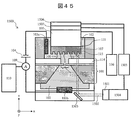
- FIG. 45 is a first example of a mechanism for adjusting the positional relationship between the nanopore device and the fixing member.
- the same components as those described above are denoted by the same reference numerals, and description thereof is omitted.
- the biomolecule measuring apparatus 1500 includes a laser irradiation unit 1501, a mirror 1503, a mechanism (relative position monitor) 1504 that feeds back data acquired by irradiation with the laser 1502, and the fixing member 107.
- the control unit 1505 can control the rotation mechanism 1506 and the adjustment mechanism 1507 using data from the relative position monitor 1504, and can control the rotation and movement of the fixing member 107 in the xy direction.
- the control unit 1505 may adjust the rotation and the xy directions of the fixing member 107 so that the groove structure imaged by laser irradiation matches the pattern formed on the nanopore device 101.
- the fixing member 107 or the nanopore device 101 including the groove 115 can also function as an alignment mechanism.
- a measurement unit control unit 1505 that images the groove structure by laser irradiation may be provided.
- the rotation and xy directions of the fixing member 107 may be adjusted by the rotation mechanism 1506 and the adjustment mechanism 1507. Thereby, the relative position between the groove structure and the nanopore device can be adjusted.
- FIG. 46 is a second example of a mechanism for adjusting the positional relationship between the nanopore device and the fixing member.
- the solution resistance itself around the nanopore device may be used.
- the biomolecule measuring device 1510 includes a rotation mechanism 1511 for the fixing member 107 in addition to the components shown in FIG.
- the drive mechanism control unit 106 receives the measured solution resistance as an input.
- the drive mechanism control unit 106 controls the rotation mechanism 1511 to rotate the fixing member 107 while monitoring the solution resistance.
- the drive mechanism control unit 106 moves the position of the groove 115 of the fixing member 107 to a desired position by rotating the shaft of the fixing member 107 while monitoring the solution resistance. Thereby, solution resistance falls.
- the configuration of FIG. 46 does not require a laser source or the like, so that the apparatus configuration can be simplified.
- Example 3 The increase in solution resistance is not limited to the problem of the conveyance control system using the fixing member 107. This is a problem that can occur even in the configuration of the nanochannel in which the structure around the nanopore 112 is narrowed to a micro-order region. Below, the structural example of the biomolecule measuring apparatus which does not use a fixing member is demonstrated.
- FIG. 47 is a schematic cross-sectional view illustrating a configuration example of a biomolecule measuring apparatus that does not use a fixing member.
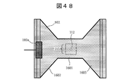
- FIG. 48 is a top view of the biomolecule measuring apparatus of FIG.
- the biomolecule measuring device 1600 includes a first liquid tank 1621 filled with the electrolyte solution 102 and a second liquid tank 1622 filled with the electrolyte solution 102.
- the first liquid tank 1621 includes a nano-sized or micro-sized channel (microchannel) 1601.
- the flow channel 1601 is a micro flow channel.
- the biomolecule measuring apparatus 1600 includes the nanopore device 101 as in the above embodiment.
- the nanopore device 101 includes a thin film 113 having nanopores 112 and a space forming member 114 having grooves 115.
- the nanopore device 101 is disposed between the first liquid tank 1621 and the second liquid tank 1622 so as to communicate the first liquid tank 1621 and the second liquid tank 1622 via the nanopore 112.
- the first electrode 103 a is disposed in the first liquid tank 1621, and the second electrode 103 b is disposed in the second liquid tank 1622.
- a power source 104 and an ammeter 109 are connected between the first and second electrodes 103a and 103b.
- the ammeter 109 is connected to an ADC (not shown) and the PC 110, and the PC 110 can record the acquired current value. Therefore, by using the ammeter 109, the arrangement information of the biomolecule can be acquired from the ion current measured when the biomolecule passes through the nanopore 112.
- the first liquid tank 1621 has an inlet 1602 and an outlet 1603. As shown in FIG. 48, a region between the inlet 1602 and the outlet 1603 and in the vicinity of the nanopore 112 is a microchannel 1601.
- the narrower the microchannel 1601, the more efficiently the biomolecule introduction efficiency into the nanopore 112, the blockage of the channel, the order of introduction of biomolecules, and the like can be controlled.
- the time constant of the circuit is reduced according to the length and cross-sectional area of the microchannel 1601.
- the space forming member 114 in contact with the first liquid tank 1621 includes a groove 115.
- the groove 115 is a region in the vicinity of the nanopore 112 in the first liquid tank 1621 and the region on the space forming member 114 within the region where the channel is narrow (that is, the channel 1601). (FIG. 47).
- the solution resistance can be increased. Therefore, it is effective to form a groove structure (or recess) on the nanopore device 101 even in the biomolecule measuring apparatus 1600 that does not use a fixed substrate.
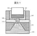
- 49 to 51 are schematic diagrams for explaining a first example of a procedure for binding a biomolecule to a fixing member and a procedure for installing the fixing member on a biomolecule measuring apparatus.
- the preparation process before the measurement includes three processes.
- the biomolecule 108 is fixed on the fixing member 107.
- the fixing member 107 and the drive mechanism 105 are connected and inserted into the upper tank of the biomolecule measuring apparatus.
- the electrolyte solution 102 is introduced into the space above and below the nanopore device 101.
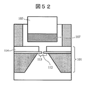
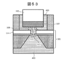
- FIG. 52 to 53 are schematic views showing a second example of the biomolecule binding procedure to the fixing member.
- the preparation process before measurement includes two processes.
- the fixing member 107 is connected to the driving mechanism 105 and inserted into the upper tank of the biomolecule measuring apparatus.
- the biomolecule mixed electrolyte solution 403 in which the biomolecule 108 in a state capable of binding to the fixing member 107 is dissolved is poured into the upper and lower tanks of the biomolecule measuring apparatus.
- the binding material for binding the biomolecule to the surface of the fixing member is preliminarily fixed in order to reduce nonspecific adsorption as much as possible and increase the density at which the target binding is performed on the surface of the fixing member. It is necessary to modify the surface of 107.
- the binding material refers to APTES and glutaraldehyde, for example, when a biomolecule is immobilized using a covalent bond via APTES glutaraldehyde. When immobilizing biomolecules using ionic bonds, it refers to an organic material on the substrate surface.
- the biomolecule is a long-chain DNA, particularly in a sequence in which a plurality of guanines are continuously arranged, strong folding of DNA becomes a problem.
- DNA is folded, a phenomenon such as clogging near the nanopore and not passing through the nanopore may occur. Therefore, it is preferable to heat the immobilizing member on which DNA is immobilized at 60 ° C. to 98 ° C. for 10 to 120 minutes in water and rapidly cool to 4 ° C. Then measure in KCl solution at 4 ° C. or room temperature.
- the driving method of the fixing member 107 includes three steps.
- the fixing member 107 in which the biomolecule 108 to be measured is fixed to the lower surface is inserted into the upper liquid tank of the biomolecule measuring device by the procedure shown in the first example or the second example.
- the electrolyte solution is introduced into the upper and lower liquid tanks, and the measurement preparation is shown.
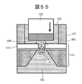
- the driving mechanism control unit 106 drives and controls the driving mechanism 105, drives the fixing member 107 downward in the z-axis, and biomolecules 108 fixed to the fixing member 107. Is placed in the potential gradient 801 generated in the vicinity of the nanopore 112 of the thin film 113. At this time, if the biomolecule 108 is negatively charged or if it is modified to be negatively charged, the biomolecule 108 receives a force from the electric field and passes through the nanopore 112 from the free end where the biomolecule 108 is not fixed. Try to move to the tank. The biomolecule 108 passes through the nanopore 112 and is stretched between the portion located in the potential gradient 801 and the end fixed on the fixing member 107. The introduction of a biomolecule into the nanopore 112 can be monitored from the ionic current.
- the driving mechanism 105 further drives the fixing member 107 downward in the z-axis direction to contact the space forming member 114 formed on the nanopore device 101, where the driving mechanism 105 The movement of the fixing member 107 is stopped. Since the space forming member 114 exists above the thin film 113, the contact between the fixing member 107 and the thin film 113 can be avoided, and the thin film 113 can be prevented from being destroyed.
- the introduction probability can be increased by stopping the driving mechanism 105 for a certain period of time.
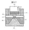
- the drive mechanism control unit 106 drives the drive mechanism 105 away from the nanopore device 101.
- the biomolecule 108 is stretched by the electric field, the biomolecule 108 is pulled by the fixing member 107 and moves upward in the nanopore 112.
- the arrangement of the biomolecule is read from the amount of change in the ionic current.
- the signal value read by the ammeter 109 is amplified as necessary and recorded in the PC 110.
- the time point when the fixing member 107 contacts the space forming member 114 in the second step is the analysis start point of the biomolecule characteristic analysis performed in the third step. Therefore, a region corresponding to the height of the space forming member 114 from the fixed point in the entire length of the biomolecule does not pass through the nanopore 112 and cannot be analyzed.
- FIG. 58 when the biomolecule 108 is fixed to the fixing member 107, the biomolecule 108 is bonded to the fixing member 107 via the linker 2001 corresponding to the height of the space forming member 114. It is possible to read all the sequences.
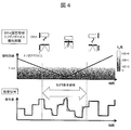
- FIG. 59 is a schematic diagram showing an example of detecting an ion current signal.
- a schematic diagram of the positional relationship of the fixing member with respect to the nanopore device is shown in the upper stage, a graph of ion current signal change is shown in the middle stage, and a graph of drive mechanism displacement is shown in the lower stage.
- the lower drive mechanism displacement z corresponds to the distance between the nanopore device 101 and the fixing member 107.
- the positional relationship between the fixing member 107 and the nanopore device 101 corresponding to the feature point in the ion current signal is shown using arrows.
- the ion current signal I 0 corresponding to the nanopore diameter is obtained.
- the speed at which the biomolecule passes through the nanopore 112 is not the driving speed of the fixing member 107 but the speed of free electrophoresis of the biomolecule. This is because when the biomolecule enters the electric field from the outside of the electric field, the biomolecule is folded and bent, so that it is not affected by the end portion being fixed to the fixing member 107.
- the ion current value acquired will indicate the average current value I b that depends on the biomolecule average diameter.
- the transport speed of the biomolecule when pulling up the biomolecule by the driving mechanism 105 is equal to the moving speed of the fixing member 107, and therefore it is necessary for the characteristic resolution. Can be transported at speed.
- the DNA nanopore passage speed is set to 100 ⁇ s or more per base from the current noise at the time of measurement and the time constant of DNA molecule fluctuation. It is considered necessary. Therefore, by controlling the driving mechanism 105 and moving the fixing member 107 upward at a speed slower than 100 ⁇ s per base, a signal reflecting the base sequence of the biomolecule can be obtained.
- the driving mechanism preferably drives the biomolecule fixing member at a speed between 34 nm / sec and 34 ⁇ m / sec.
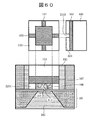
- FIG. 60 is a schematic diagram showing a first example of a stop mechanism for preventing contact between the fixing member and the thin film. In order to simplify the description, the illustration of the groove 115 is omitted.
- FIG. 60 also shows a schematic side view of the fixing member 107 including the driving mechanism 105 and a bottom view having the slit 603.
- the space forming member 2201 is provided so as to protrude downward from the lower surface of the fixing member 107 instead of on the nanopore device 101.
- the space forming member 2201 is formed on the outer periphery of the lower surface of the fixing member 107 or on the four corners of the lower surface or on the two opposite sides so as to contact the nanopore device 101 at a position outside the thin film 113.
- the space forming member 2201 is provided on at least a part of the outer side of the region facing the thin film 113 on the lower surface of the fixing member 107.
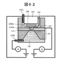
- 61 to 62 are schematic views showing a second example of a stop mechanism for preventing contact between the fixing member and the thin film.
- the illustration of the groove 115 is omitted.
- 61 shows a state before the fixing member 107 contacts the nanopore device 101
- FIG. 62 shows a state after the fixing member 107 contacts the nanopore device 101.
- the stop mechanism only needs to create a space between the fixing member 107 and the thin film 113 so as to avoid contact between them.
- an electrode 2302a and an electrode 2302b are arranged on at least a part of the outer surface corresponding to the thin film on the upper surface of the nanopore device 101 and the lower surface of the fixing member 107, respectively.
- the relative distance between the fixed member 107 and the nanopore device 101 is detected from the change in capacitance, and the contact between the two is monitored.
- the voltage applied between the electrodes 2302a and 2302b is selected according to the assumed current amount and the measurement current. Moreover, in order to prevent corrosion and oxidation of an electrode, it is also possible to measure by applying a pulse voltage.
- the driving mechanism control unit 106 (not shown) drives the fixing member 107 in the direction of the nanopore device 101 by the driving mechanism 105, and signals acquired from the electrodes 2302a and 2302b when the nanopore device 101 and the fixing member 107 come close to each other. The distance between the two is detected based on the change, and the drive of the drive mechanism 105 is stopped.
- the drive mechanism control unit 106 can also monitor the contact from a short circuit instead of acquiring a capacitance change signal. While a voltage is applied between the electrodes 2302a and 2302b constituting the stop mechanism, no voltage is applied to the first and second electrodes 103a and 103b for measurement.
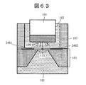
- 63 to 64 are schematic views showing a third example of a stop mechanism for preventing contact between the fixing member and the thin film.
- the illustration of the groove 115 is omitted.
- the electrodes 2401 and 4022 are arranged only on the nanopore device 101 and the electrodes are wired, and the fixing member 107 and the nanopore device are detected from the change in the amount of current when the fixing member 107 approaches the nanopore device 101. The relative distance between 101 is detected.
- the electrodes 2401 and 2402 are disposed at the outer periphery, four corners, or two opposite sides of the region outside the thin film 113 on the upper surface of the nanopore device 101. In the example shown in FIG.
- electrodes 2403 and 2404 are arranged on the lower surface of the fixing member 107 and the electrodes are wired, and the relative distance between the fixing member 107 and the nanopore device 101 is detected by the same mechanism.
- the electrodes 2403 and 2404 may be disposed at the four corners outside the region corresponding to the thin film 113 or the two opposite sides of the lower surface of the fixing member 107.
- the groove 115 may be formed on the side where the electrodes 2401 and 2402 are disposed (the fixing member 107 or the nanopore device 101), or the side where the electrodes 2401 and 4022 are not disposed (the fixing member 107 or the nanopore device 101). May be formed.
- the drive mechanism 105 may be provided with an inclination adjustment function, and the drive mechanism control unit 106 may adjust the inclination of the drive mechanism 105 so that the current values acquired from the four locations substantially match.
- independent goniometers may be provided at four corners, and may be adjusted manually or automatically based on current values acquired from four locations.
- FIG. 65 to 67 are schematic top views showing examples of electrode arrangement on the nanopore device 101 shown in FIG.
- FIG. 65 is a layout diagram of the thin film 113, sensor wiring 2406, and electrode extraction wiring 2407 on the nanopore device 101.
- 66 and 67 are enlarged views of the sensor wiring.
- FIG. 66 shows an example of a type of counter electrode
- FIG. 67 shows an example in which counter electrodes 2408 are arranged in a ring shape at four locations around the thin film 113.
- a voltage of 1 V is applied between electrodes designed with an electrode length L of 10 ⁇ m and an electrode interval s of 0.4 ⁇ m to 2 ⁇ m shown in FIG. 66, and then the fixing member 107 is brought close to the nanopore device 101. The current change between the electrodes was monitored.
- FIG. 68 is a graph showing the relationship between the distance h and the current amount normalized by the amount of current flowing when the distance h between the fixing member and the nanopore device is 10 ⁇ m.
- the height of the fixing member 107 can be adjusted by acquiring the correlation between the distance h and the current amount.
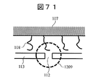
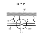
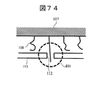
- FIGS. 69 to 72 and FIGS. 73 to 74 are schematic cross-sectional views showing examples of the driving method of the fixing member by the biomolecule measuring apparatus having the biomolecule pre-stretching mechanism. In order to simplify the description, the illustration of the groove 115 is omitted.
- the biomolecule measuring apparatus of this example includes electrodes 1202a and 1202b on the fixing member 107 and the nanopore device 101, respectively.
- the circuit conversion controller 2706 connects a power source to the circuit 1207 connected to the electrodes 1202 a and 1202 b to create a potential gradient 1203 between the fixing member 107 and the nanopore device 101.
- the potential gradient 1203 due to the potential gradient 1203, the negatively charged biomolecule 108 is stretched between the fixing member 107 and the nanopore device 101.
- the drive mechanism 105 is driven to drive downward until the fixing member 107 contacts the space forming member 114 of the nanopore device 101.
- the drive mechanism 105 is driven to drive downward until the fixing member 107 contacts the space forming member 114 of the nanopore device 101.
- a power source is connected to the circuit 1208 connected to the first and second electrodes 103a and 103b, it is within the range of an assumed electric field 1209 that should be generated around the nanopore.
- a biomolecule 108 is inserted.
- the circuit 1207 connected to the electrodes 1202a and 1202b changes to a circuit 1208 that forms an electric field around the nanopore. And switch the power connection.
- FIG. 74 by forming a potential gradient 801 around the nanopore, the tip of the biomolecule 108 is inserted into the nanopore.
- the tip of the biomolecule 108 when the tip of the biomolecule 108 does not enter the nanopore 112 and the probability is small, the tip of the biomolecule 108 enters the nanopore 112 as shown in the enlarged view of FIG. There are cases. Only when the tip of the biomolecule 108 enters the electric field region without entering the nanopore 112, the base can be read from the tip of the biomolecule 108.
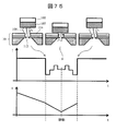
- FIG. 75 is a schematic diagram showing an example of a signal read from the tip of a biomolecule.
- the graph of the ion current signal change is shown in the middle, and the graph of the drive mechanism displacement is shown in the lower.
- the lower drive mechanism displacement z corresponds to the distance between the nanopore device 101 and the fixing member 107.
- the correspondence between the fixing member 107 and the nanopore device 101 shown in the upper part is indicated by an arrow.
- the ion current signal I 0 corresponding to the nanopore diameter is obtained.
- the tip of the biomolecule 108 is in the potential gradient 801 (see FIG. 74).
- the mechanism 105 is driven below the z-axis, the biomolecule 108 is sequentially introduced into the nanopore 112 from the free end. At this time, since there is no bending in the biomolecule 108, the biomolecule 108 is driven at a speed set by the drive mechanism control unit 106, and the characteristic analysis corresponding to each arrangement of the biomolecule 108 becomes possible.
- the signal read in the time until it exits from the nanopore 112 becomes a symmetric signal with the contact time as the center.
- Reading of the biomolecule 108 different from the biomolecule 108 measured first among the plurality of biomolecules 108 fixed to the fixing member 107 can be realized by driving the drive mechanism 105 in the xy direction.
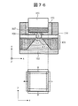
- FIG. 76 is a schematic cross-sectional view of a part of the biomolecule measuring apparatus and a schematic top view of the drive mechanism 105. As shown in the schematic top view, by driving the driving mechanism 105 in the xy direction, that is, in a direction parallel to the surface of the thin film 113, another biomolecule 108 can be passed through the nanopore 112, and on the fixing member 107. Analysis of multiple biomolecules is realized.
- FIG. FIG. 77 is a schematic cross-sectional view showing the positional relationship between the thin film 113 having the nanopore 112 and the fixing member 107 when the characteristic analysis of the first biomolecule 1405 is performed.
- the driving mechanism 105 moves the fixing member 107 in parallel to the surface of the thin film 113 by the same distance as the diameter of the potential gradient 801.
- FIG. 78 is a schematic cross-sectional view showing the positional relationship between the thin film 113 having the nanopore 112 after movement and the fixing member 107.
- Example 5 An example of a procedure for measuring a biomolecule using the biomolecule measuring apparatus will be described below.
- the ionic current I flowing through the nanopore is measured through an amplifier.
- a constant voltage is applied between the pair of Ag / AgCl electrodes respectively inserted into the upper and lower liquid tanks, and the ion current amount I 0 corresponding to the size of the nanopore is acquired.
- FIG. 79 is an explanatory diagram showing an example of a method for reading the base sequence of DNA as a biomolecule.
- the upper part of FIG. 79 shows two typical positional relationships between the fixing member 107 and the nanopore device 101 during DNA base sequence analysis.
- the middle part of FIG. 79 shows changes in ion current, and the lower part shows displacement of the fixing member 107.
- the lower displacement z corresponds to the distance between the fixing member 107 and the nanopore device 101.
- the driving direction of the fixing member 107 by the driving mechanism 105 is changed, the positional relationship between the fixing member 107 and the nanopore device 101 at that time is shown in the drawing.
- the middle black arrow indicates that the first positional relationship illustrated on the upper left side is taken, and the white arrow indicates that the second positional relationship illustrated on the upper right side is taken.
- the fixing member 107 When the fixing member 107 is driven below the z-axis by the driving mechanism 105, the free end of the biomolecule 108 enters the nanopore 112, and the biomolecule 108 is stretched between the end fixed to the fixing member 107 and the nanopore 112. . At this time, the ionic current decreases according to the average diameter size of the biomolecule 108 and becomes I b .
- the biomolecule 108 enters the potential gradient 801 from the outside, the biomolecule 108 is folded, so that it passes through the nanopore 112 at the speed of free electrophoresis of the biomolecule 108 instead of the moving speed of the fixing member 107. become.
- the ion current value at that time is not a current value derived from each base but an average current value I b depending on the average diameter of the biomolecule 108.
- the fixing member 107 is further driven below the z-axis by the drive mechanism 105, but the space-forming member 114 prevents the movement below the z-axis and stops the movement.
- the positional relationship among the fixing member 107, the biomolecule 108, and the nanopore device 101 at this time is shown as the first positional relationship on the upper left in FIG.
- the transport speed of the biomolecule 108 when pulling up the biomolecule 108 is equal to the driving speed of the fixing member 107, and therefore the biomolecule 108 can be transported at a speed required for monobase decomposition ( ⁇ 3.4 nm / ms). . Therefore, a signal reflecting the base sequence of the biomolecule 108 is obtained.
- the sequence information of the biomolecule 108 that moves in the nanopore 112 can be read.
- the biomolecule 108 While the free end of the biomolecule 108 that is not fixed exits from the nanopore 112 and enters the potential gradient 801 around the nanopore, the biomolecule 108 is removed from both the fixing member 107 and the potential gradient 801 around the nanopore. It receives a reverse force and is stretched.
- the relationship between the fixing member 107, the biomolecule 108, and the nanopore device 101 at this time is shown as the second positional relationship in the upper right of FIG. Further, since the biomolecule 108 escapes from the nanopore 112, the amount of ionic current returns to I 0 . This change in current value is detected, and driving of the fixing member 107 by the driving mechanism 105 is stopped.
- the driving mechanism 105 drives the fixing member 107 downward in the z-axis to pass the biomolecule 108 from the free end to the nanopore 112, while reading the base sequence of the biomolecule 108.
- the biomolecule 108 is stretched as a whole. Therefore, since the biomolecule 108 passes through the nanopore 112 from the free end thereof at a driving speed by the driving mechanism 105, it is possible to read a signal with high accuracy.
- the array read while being driven above the z-axis is read from the opposite direction, and an ion current that changes symmetrically is reflected.
- the displacement 1530 from the position where the fixing member 107 and the nanopore device 101 contact to the position where the ionic current value becomes I 0 reflects the length of the biomolecule 108.
- Example 6 Next, an embodiment in which biomolecule measuring devices are arranged in parallel will be described.
- the biomolecule measuring apparatus described above has good affinity with parallel nanopore devices. Since parallel biomolecules of the same kind can be measured simultaneously, the throughput can be improved.
- three types of examples for parallelization are shown.
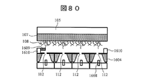
- FIG. 80 and 81 are schematic cross-sectional views showing a first example of a biomolecule measuring apparatus having parallel nanopore devices. In order to simplify the description, the illustration of the groove 115 is omitted. As shown in FIG. 80, in this example, a plurality of nanopore devices 1604 are arranged adjacent to each other in the lateral direction, and a common drive mechanism 105 and fixing member 107 are arranged on the top of the plurality of nanopore devices 1604. Yes.
- the fixing member 107 has an area sufficient to cover the entire plurality of nanopore devices 1604.
- Each of the plurality of nanopore devices 1604 arranged in parallel includes an independent liquid tank, and one of the array electrodes 1608 is arranged in the liquid tank of each nanopore device 1604, and each of the array electrodes 1608 is connected to an amplifier.
- One liquid tank is provided in common above the plurality of nanopore devices 1604 arranged in parallel, and a common electrode 1609 is arranged in the liquid tank with respect to the array electrode 1608.
- a space forming member 1610 common to the plurality of nanopore devices 1604 is provided on the side of the parallel nanopore devices 1604.
- the liquid tank provided in each nanopore device 1604 communicates with the upper liquid tank via each nanopore 112 provided in the nanopore device 1604.
- a plurality of biomolecules 108 are bonded to the lower surface of the fixing member 107. As shown in FIG. 81, when the drive mechanism 105 is lowered below the z-axis, the biomolecule 108 on the fixing member 107 passes through the nanopores 112 provided in each nanopore device 1604. According to this embodiment, a plurality of biomolecules can be measured in parallel using a plurality of nanopores 112, so that the measurement throughput is increased.
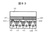
- FIG. 82 and 83 are schematic cross-sectional views showing a second example of a biomolecule measuring apparatus having parallel nanopore devices. In order to simplify the description, the illustration of the groove 115 is omitted.
- one drive mechanism 105 is arranged on top of a plurality of arranged nanopore devices 1604.
- An array electrode 1608 is connected to the nanopore device 1604.
- One liquid tank is provided in common above the plurality of nanopore devices 1604, and a common electrode 1609 is disposed for each array electrode 1608.
- a space forming member 1610 common to the plurality of nanopore devices 1604 is provided on the side of the parallel nanopore devices 1604.
- a plurality of fixing members are connected to the drive mechanism 105, and different types of biomolecules are fixed thereto. This makes it possible to simultaneously analyze the characteristics of different biomolecules.
- the driving mechanism 105 is connected to two biomolecule fixing members, a first fixing member 107 and a second fixing member 1605.
- the first biomolecule 108 is bonded to the first fixing member 107
- the second biomolecule 1606 is bonded to the second fixing member 1605.
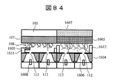
- FIGS. 84 and 85 are cross-sectional schematic diagrams showing a third example of a biomolecule measuring apparatus having parallel nanopore devices.
- the illustration of the groove 115 is omitted.
- a plurality of drive mechanisms are arranged on top of a plurality of arranged nanopore devices 1604.
- a fixing member is connected to each driving mechanism, and another type of biomolecule is fixed to each fixing member.
- a space forming member can also be provided for each fixed member.
- the first drive mechanism 105 and the second drive mechanism 1607 are arranged above the plurality of nanopore devices 1604.
- a first fixing member 107 is connected to the first driving mechanism 105, and a second fixing member 1605 is connected to the second driving mechanism 1607.
- the first biomolecule 108 is bonded to the first fixing member 107
- the second biomolecule 1606 is bonded to the second fixing member 1605.
- a first space forming member 1611 is provided for the first fixing member 107
- a second space forming member 1612 is provided for the second fixing member 1605.
- the first space forming member 1611 and the second space forming member 1612 have different film thicknesses. Thereby, independent height adjustment is possible even for biomolecules having different lengths.
- the first and second space forming members 1611 and 1612 are formed with slits and the like.
- the solution filling the upper part of the nanopore 112 does not become independent for each sample. It has become a structure. Accordingly, the common electrode 1609 may be the only electrode disposed on the plurality of nanopores 112.
- the size relationship between the number of nanopores a and the number of biomolecules b on the fixing member is a ⁇ b, and the biomolecules are tightly coupled to the fixing member, thereby fixing the fixing member to the nanopore. Biomolecules are always introduced into the nanopores when lowered vertically toward the device.
- Example 7 An embodiment using magnetic beads as another means for fixing a biomolecule to a fixing member will be described.
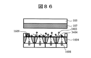
- an example using the apparatus shown in FIGS. 86 to 88 as a biomolecule measuring apparatus will be described.
- the fixing member is made of a magnet material.
- 86 to 88 are schematic cross-sectional views illustrating a procedure for measuring a biomolecule fixed to a fixing member using magnetic beads.
- the illustration of the groove 115 is omitted.
- Biomolecules prepared in advance on magnetic beads are prepared.
- a voltage is applied between the Ag / AgCl electrode 1608 and the common electrode 1609 arranged in the paralleled nanopore device 1604, and in the electrolyte solution around each nanopore. Then, an electric field is generated, the biomolecule 3404 fixed to the magnetic beads 3403 is migrated by electrophoresis, and the biomolecule is introduced into the nanopores of the nanopore device 1604 arranged in parallel.
- the ionic current derived from each nanopore can be monitored, and the effective nanopore device in which the biomolecule has entered the nanopore can be confirmed from the rate of change of the ionic current.
- the driving member 105 drives the fixing member 107 toward the nanopore device 1604 as indicated by the arrow.
- the magnetic beads 3403 are attracted and fixed to the fixing member 107 by magnetic force.
- the fixing member 107 is driven at a controlled speed in the direction away from the nanopore device 1604 by the driving mechanism 105, and is caused by the biomolecule moving in the nanopore.
- the ion current that changes is detected by the ammeter 109 and recorded in the PC 110.
- the driving mechanism 105 made of a piezoelectric element can drive the fixing member 107 at an arbitrary speed.
- the DNA immobilized on the magnetic beads can be driven at a speed of 3.4 nm / ms or less. Therefore, it is possible to read with high accuracy by moving the inside of the nanopore.
- the initial alignment between the nanopore and the biomolecule is unnecessary.
- it is possible to introduce biomolecules into the nanopores by diffusing into the electric field generated in the vicinity of the nanopores it is possible to reduce the probability that there are nanopores that do not pass through the biomolecules in the paralleled nanopores. it can.
- FIG. 89 is a diagram illustrating how the blocking current is eliminated when the fixing member is driven by the driving mechanism.
- the fixing member 107 in which ss-poly (dA) having a chain length of 5 k was fixed to the surface modified with APTES / glutaraldehyde was brought close to the nanopore 112 of the nanopore device 101.
- FIG. 89 (a) shows the blocking signal, and when the fixing member 107 was separated from the nanopore device 101, the blocking signal was eliminated.
- FIG. 89 (b) shows the locus of the fixing member 107 at the same time as FIG. 89 (a).
- the nanopore device 101 and the fixing member 107 approach each other. About 1 second after confirming the decrease in the ion current, the driving of the fixing member 107 by the driving mechanism 105 was stopped. About 10 seconds later, the distance between the nanopore device 101 and the fixing member 107 began to increase, and when the ion current increased again (after 30 seconds had elapsed), the driving by the driving mechanism 105 was stopped again. When the fixing member 107 on which the DNA is fixed is brought closer to the nanopore 112, the ionic current decreases, and when the DNA is fixed away from the nanopore 112, the original current value is restored. This indicates that DNA is introduced into and extracted from the nanopore 112 by driving the fixing member 107 by the driving mechanism 105.
- the time from when the driving mechanism 105 is started to move the fixing member 107 away from the nanopore device 101 to the time when the blocking signal is canceled (DNA driving time) is defined as t out as shown in FIG. 89 (b).
- DNA driving time The time from when the driving mechanism 105 is started to move the fixing member 107 away from the nanopore device 101 to the time when the blocking signal is canceled (DNA driving time) is defined as t out as shown in FIG. 89 (b).
- the moving speed of the fixed member 107 was obtained from the relationship with the counter speed corresponding to the set speed of the drive mechanism 105.
- FIG. 90 shows the relationship between the DNA driving time (t out ) acquired with respect to the moving speed of each fixing member 107.
- the plots in FIG. 90 are experimental values.
- the DNA driving distance that is, the maximum length introduced into the DNA nanopore 112 is determined by the position where the driving of the fixing member 107 stops after the nanopore 112 is blocked by DNA.
- the fixing member 107 When the fixing member 107 is driven by the driving mechanism 105, the blocking signal indicating that the DNA has entered the nanopore 112 is visually confirmed and manually stopped. Therefore, after the DNA actually enters the nanopore 112, the fixing member 107 is driven. It is considered that it takes about 1 second at the shortest to stop driving. Accordingly, DNA of about 60-100 nm is surely entered into the nanopore 112 at the shortest.
- the solid line is the calculated value of the maximum DNA driving time obtained from the length of the fixed DNA.
- the broken line is a calculated value of the minimum DNA driving time required when 60 nm of DNA enters. Since the experimentally measured DNA driving time is within the range from the solid line to the broken line, the obtained blocking signal is derived from the DNA on the fixing member, and the measured value is reasonable. It is believed that there is. Further, the actually measured DNA driving time is distributed in a direction in which the DNA driving time becomes longer as the moving speed of the fixing member 107 becomes slower. This is considered to indicate that the DNA on the fixing member 107 is transported through the nanopore 112 depending on the driving speed of the driving mechanism 105.
- FIG. 91 is a diagram showing a result of measurement in which a molecule ((dA50dC50) m) obtained by repeatedly stretching a dA50dC50 polymer was similarly bonded to a fixing member.
- a blocking signal as obtained in FIG. 89 was confirmed. Analyzing the current after blockade, we obtained a two-level signal. As described above, it is possible to measure the state in which the blocking signal intensity varies depending on the molecular species by binding the biomolecule to the fixing member and decreasing the molecular passage speed.
- porous silica may be used as a material for the fixing member in addition to forming the groove structure.
- the biomolecule fixing member may be made of porous silica, or at least a part of the fixing member may be made of porous silica.
- the surface of the fixing member that approaches the nanopore device may be made of porous silica. In this configuration, the biomolecule to be measured is fixed to at least the outermost surface of the porous silica (the surface facing the nanopore device).
- Porous silica has pores on the surface and inside. For example, by providing porous silica on the surface of the fixing member, the solution can pass through the pores when the fixing member approaches the nanopore device. Thereby, it is possible to suppress an increase in passage resistance that occurs when the fixing member approaches the nanopore device.
- FIG. 92 shows a means for forming a biomolecule fixing member partially made of porous silica.
- a coating liquid 3501 in which a silica precursor and a surfactant are mixed is applied to the surface of the silicon substrate 107 as a fixing member.
- micelle aggregates are formed in the coating solution.
- Reference numeral 3504 denotes pores formed after the micelle aggregate 3502 is removed.
- the surfactant is a cationic surfactant and more preferably has a hydrophobic group having 16 or more carbon atoms, or a hydrophobic group such as a benzyl group or a phenyl group.
- the micelle size is determined, and the average pore diameter generated after sintering varies in the range of 3 nm or more and less than 5 nm. For example, when a surfactant having a carbon chain C18 is used, an average pore diameter of 3.5 nm can be formed.
- the pore volume varies in the range of 0.1 to 2.0 cm 3 / g, and can be controlled at a minimum of 20% or more of the silica volume.
- it is necessary to reduce the density of the structure by about 100 times. Therefore, it is necessary to realize a density reduction of 99% or more by volume ratio, and this is within the controllable range of this structure.
- the aqueous solution needs to penetrate into the pores.
- This matter can be solved by hydrophilizing the porous silica surface.
- organosilicon compound having an amino group-modified siloxane bond Organosilicon compounds having a siloxane bond are also useful for reinforcing the skeleton of the porous structure.
- the porous silica is a solid silicon material, it is possible to set a hydroxyl group at the silicon terminal by plasma irradiation and modify the amino group at the terminal by using APTES, and a crosslinking agent having a carboxyl terminal such as glutaraldehyde. In addition, it is possible to fix biomolecules that have been amino-terminally treated.
- the present invention is not limited to the above-described embodiments, and includes various modifications.
- the above embodiments have been described in detail for easy understanding of the present invention, and are not necessarily limited to those having all the configurations described.
- a part of the configuration of one embodiment can be replaced with the configuration of another embodiment.
- the structure of another Example can also be added to the structure of a certain Example.
- another configuration can be added, deleted, or replaced.
- Each configuration, function, and the like of the measurement unit and the control unit described above may be realized by software by interpreting and executing a program that realizes each function by the processor.
- Information such as programs, tables, and files for realizing each function can be stored in a recording device such as a memory, a hard disk, an SSD (Solid State Drive), or a recording medium such as an IC card, an SD card, or a DVD.
- a recording device such as a memory, a hard disk, an SSD (Solid State Drive), or a recording medium such as an IC card, an SD card, or a DVD.
- each configuration, function, and the like of the measurement unit and the control unit described above may be realized in hardware by designing a part or all of them, for example, with an integrated circuit.
Landscapes
- Health & Medical Sciences (AREA)
- Life Sciences & Earth Sciences (AREA)
- Chemical & Material Sciences (AREA)
- Engineering & Computer Science (AREA)
- Physics & Mathematics (AREA)
- Molecular Biology (AREA)
- Biomedical Technology (AREA)
- Biochemistry (AREA)
- General Health & Medical Sciences (AREA)
- Pathology (AREA)
- Analytical Chemistry (AREA)
- Immunology (AREA)
- General Physics & Mathematics (AREA)
- Spectroscopy & Molecular Physics (AREA)
- Bioinformatics & Cheminformatics (AREA)
- Chemical Kinetics & Catalysis (AREA)
- Electrochemistry (AREA)
- Nanotechnology (AREA)
- Wood Science & Technology (AREA)
- Organic Chemistry (AREA)
- Genetics & Genomics (AREA)
- Zoology (AREA)
- Biotechnology (AREA)
- Biophysics (AREA)
- Medicinal Chemistry (AREA)
- General Engineering & Computer Science (AREA)
- Hematology (AREA)
- Urology & Nephrology (AREA)
- Food Science & Technology (AREA)
- Microbiology (AREA)
- Microelectronics & Electronic Packaging (AREA)
- Sustainable Development (AREA)
- Plant Pathology (AREA)
- Apparatus Associated With Microorganisms And Enzymes (AREA)
- Investigating Or Analyzing Materials By The Use Of Electric Means (AREA)
- Measuring Or Testing Involving Enzymes Or Micro-Organisms (AREA)
Abstract
Description
本発明の搬送制御機構を有する生体分子測定装置、及びその装置を用いた生体分子の配列読取の例について説明する。図1は、生体分子測定装置の構成例を説明する断面模式図である。
τ=(RL+Rg)Cs
となる。
Rg=L/σWh
で表現される。
R1 = (L-nL1)/(Wh0+w1h1n)
tn=10-3+(1/6)(n-1)-10-3+(1/6)(n-2) for n>2
で決定される。
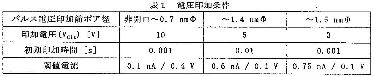
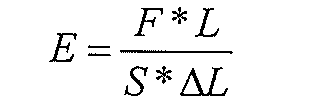


次に、溝構造を利用した位置合わせ機構について説明する。図45は、ナノポアデバイスと固定部材との間の位置関係を調節する機構の第1の例である。図45において、上述した構成要素と同じ構成要素については、同じ符号を付して、それらの説明を省略する。
溶液抵抗の上昇は、固定部材107を用いた搬送制御システムの課題には限らない。ナノポア112周辺の構造がマイクロオーダーの領域に狭められているナノ流路の構成においても、起こりうる課題である。以下では、固定部材を用いない生体分子測定装置の構成例を説明する。
図49~図51は、固定部材への生体分子の結合手順及び固定部材の生体分子測定装置への設置手順の第1の例を説明する模式図である。説明を簡単にするために、電極及び溝115の図示を省略している。測定前の準備工程は3つの工程を含む。図49に示す第1の工程では、固定部材107上に生体分子108を固定する。図50に示す第2の工程では、固定部材107と駆動機構105を接続し、生体分子測定装置の上槽に挿入する。図51に示す第3の工程では、ナノポアデバイス101の上下の空間に電解質溶液102を導入する。
生体分子測定装置を用いて生体分子を測定する手順の実施例を以下に述べる。以下の全ての工程において、ナノポアを介して流れるイオン電流Iは増幅器を通して計測されている。また、上下2槽の液槽に各々挿入された一対のAg/AgCl電極間には一定の電圧が印加されており、ナノポアのサイズに応じたイオン電流量I0が取得されている。
次に、生体分子測定装置を並列化した実施例について説明する。上記で説明した生体分子測定装置は、並列化したナノポアデバイスとの親和性が良い。並列化により同種の生体分子を同時に測定可能となるため、スループットの向上を測ることが可能となる。ここでは、並列化に対する3種類の例を示す。
生体分子を固定部材に固定するための他の手段として磁気ビーズを用いた実施例を示す。ここでは、生体分子測定装置として図86~図88に示した装置を用いる例によって説明する。ただし、固定部材は磁石材料によって構成する。
図89は、駆動機構による固定部材の駆動に伴う封鎖電流解消の様子を示す図である。図1に示した生体分子測定装置を用い、APTES/グルタルアルデヒド修飾した表面に鎖長5kのss-poly(dA)を固定した固定部材107をナノポアデバイス101のナノポア112近傍まで近づけた。その結果、図89(a)に示すように、封鎖信号が確認され、固定部材107をナノポアデバイス101から離すと、封鎖信号が解消した。図89(b)に、図89(a)と同一時間での固定部材107の軌跡を示す。カウンタ変位が増えるにつれ、ナノポアデバイス101と固定部材107は近接する。イオン電流の減少を確認してから約1秒後に、駆動機構105による固定部材107の駆動を停止した。約10秒後に、ナノポアデバイス101と固定部材107との間の距離を離し始め、再び、イオン電流が増大した時点で(30秒経過後に)再び駆動機構105による駆動を停止させた。DNAを固定した固定部材107をナノポア112に近づけるとイオン電流が減少し、ナノポア112から遠ざけることで元の電流値に戻った。これは、駆動機構105による固定部材107の駆動により、DNAのナノポア112への導入、引き抜きが生じたことを示している。
溶液抵抗の低減を実現するその他の手法として、溝構造を形成する他に、固定部材の材料として、ポーラスシリカを用いてもよい。生体分子の固定部材が、ポーラスシリカで形成されるか、又は、固定部材における少なくとも一部がポーラスシリカで構成されてもよい。例えば、固定部材におけるナノポアデバイス(生体分子計測デバイス)に接近する表面がポーラスシリカで構成されてもよい。この構成において、ポーラスシリカの少なくとも最表面(ナノポアデバイスに対向する面)に計測対象である生体分子が固定される。
101 ナノポアデバイス
102 電解質溶液
103a、103b Ag/AgCl電極
104 電源
105 駆動機構
106 駆動機構制御ユニット
107 生体分子固定部材
108 生体分子
109 電流計
110 PC
111 接続部材
112 ナノポア
113 薄膜
114 空間形成部材
115 溝
115a 溝の凸部
115b 溝の凹部
1501 レーザ照射ユニット
1503 ミラー
1504 相対位置モニタ
1505 制御ユニット
1506、1511 回転機構
1507 調整機構
3501 シリカ前駆体と界面活性剤を混合した塗布液
3502 ミセル集合体
3503 多孔質シリカ膜
3504 細孔
Claims (16)
- 電解質溶液が満たされる第1の液槽と、
電解質溶液が満たされる第2の液槽と、
ナノポアを有する薄膜を支持し、前記ナノポアを介して前記第1の液槽と前記第2の液槽を連通するように前記第1の液槽と前記第2の液槽の間に設けられたナノポアデバイスと、
前記第1の液槽に配置され、前記薄膜より大きなサイズを有し、生体分子が固定される固定部材と、
前記固定部材を前記薄膜に対して近づく方向あるいは遠ざかる方向に駆動する駆動機構と、
前記第1の液槽に設けられた第1の電極と、
前記第2の液槽に設けられた第2の電極と、
前記固定部材と前記薄膜との接触を防止するストップ機構と、
前記第1の電極と前記第2の電極との間に電圧を印加する電源と、
前記第1の電極と前記第2の電極の間に流れるイオン電流を計測する測定部とを備え、
前記ナノポアデバイス及び前記固定部材の少なくとも一方は、前記ナノポアデバイス及び前記固定部材が対向する領域に溝構造を備えており、
前記測定部は、前記固定部材に固定された前記生体分子が前記ナノポアを通過するとき計測されるイオン電流により当該生体分子の配列情報を取得することを特徴とする生体分子測定装置。 - 請求項1に記載の生体分子測定装置において、
前記溝構造が、前記ナノポアデバイスと前記固定部材とが対向している範囲で連続的に形成されていることを特徴とする生体分子測定装置。 - 請求項1に記載の生体分子測定装置において、
前記ストップ機構は、前記ナノポアデバイス上に配置され、前記固定部材と前記薄膜との間に空間を形成する空間形成部材であり、
前記溝構造が、前記空間形成部材に形成されていることを特徴とする生体分子測定装置。 - 請求項1に記載の生体分子測定装置において、
前記溝構造の断面は、矩形、三角形、半月形、又は台形であることを特徴とする生体分子測定装置。 - 請求項1に記載の生体分子測定装置において、
前記生体分子は、前記溝構造の凸部に固定されていることを特徴とする生体分子測定装置。 - 請求項1に記載の生体分子測定装置において、
前記溝構造の凸部及び凹部は、同一材料で形成されていることを特徴とする生体分子測定装置。 - 請求項1に記載の生体分子測定装置において、
前記溝構造の凸部及び凹部は、異なる材料で形成されていることを特徴とする生体分子測定装置。 - 請求項1に記載の生体分子測定装置において、
前記固定部材には、複数の異なるマーカを介して複数種の生体分子が固定されていることを特徴とする生体分子測定装置。 - 請求項1に記載の生体分子測定装置において、
前記溝構造の掘り込み深さは、5μm以上であることを特徴とする生体分子測定装置。 - 請求項1に記載の生体分子測定装置において、
前記溝構造の凸部の幅は、前記固定部材に固定される前記生体分子のピッチ以上であることを特徴とする生体分子測定装置。 - 請求項1に記載の生体分子測定装置において、
前記駆動機構が、前記固定部材を前記ナノポアデバイスに接触させる機能を備えており、前記溝構造は、前記ナノポアデバイスと前記固定部材とが対向している範囲の全域で連続して形成されていることを特徴とする生体分子測定装置。 - 請求項1に記載の生体分子測定装置において、
前記固定部材の移動又は回転を調節する調節機構と、
前記溝構造にレーザを照射するレーザ照射機構と、
前記調節機構を制御する制御ユニットとを備え、
前記制御ユニットは、前記レーザの照射によって得られた画像を用いて前記調節機構を制御することを特徴とする生体分子測定装置。 - 請求項1に記載の生体分子測定装置において、
前記固定部材の移動又は回転を調節する調節機構と、
前記調節機構を制御する制御ユニットとを備え、
前記制御ユニットは、前記ナノポアデバイスの周辺の溶液抵抗をモニタすることにより、前記調節機構を制御することを特徴とする生体分子測定装置。 - 電解質溶液が満たされる第1の液槽と、
電解質溶液が満たされる第2の液槽と、
ナノポアを有する薄膜を支持し、前記ナノポアを介して前記第1の液槽と前記第2の液槽を連通するように前記第1の液槽と前記第2の液槽の間に設けられたナノポアデバイスと、
前記第1の液槽に設けられた第1の電極と、
前記第2の液槽に設けられた第2の電極と、
前記第1の電極と前記第2の電極との間に電圧を印加する電源と、
前記第1の電極と前記第2の電極の間に流れるイオン電流を計測する測定部とを備え、
前記第1の液槽は、前記ナノポアの近傍の領域に微小流路を備え、
前記ナノポアデバイスは、溝構造を備え、
前記測定部は、生体分子が前記ナノポアを通過するとき計測されるイオン電流により当該生体分子の配列情報を取得することを特徴とする生体分子測定装置。 - 生体分子測定装置において生体分子を固定するための固定部材であって、
当該固定部材の表面に溝構造が形成されていることを特徴とする固定部材。 - 請求項1に記載の生体分子測定装置において、
前記固定部材はポーラスシリカで形成されている、又は、前記固定部材における前記ナノポアデバイスに接近する面の表面に前記ポーラスシリカが設けられており、
前記ポーラスシリカにおける前記ナノポアデバイスに対向する面に計測対象の前記生体分子が固定されていることを特徴とする生体分子測定装置。
Priority Applications (5)
| Application Number | Priority Date | Filing Date | Title |
|---|---|---|---|
| US15/779,931 US10753922B2 (en) | 2015-12-17 | 2016-11-29 | Biomolecule measurement apparatus |
| CN201680071179.7A CN108368466B (zh) | 2015-12-17 | 2016-11-29 | 生物体分子测定装置 |
| DE112016005255.3T DE112016005255B4 (de) | 2015-12-17 | 2016-11-29 | Biomolekülmesseinrichtung |
| GB1809149.6A GB2560668B (en) | 2015-12-17 | 2016-11-29 | Biomolecule measurement apparatus |
| JP2017555957A JP6826047B2 (ja) | 2015-12-17 | 2016-11-29 | 生体分子測定装置 |
Applications Claiming Priority (2)
| Application Number | Priority Date | Filing Date | Title |
|---|---|---|---|
| JP2015246702 | 2015-12-17 | ||
| JP2015-246702 | 2015-12-17 |
Publications (1)
| Publication Number | Publication Date |
|---|---|
| WO2017104398A1 true WO2017104398A1 (ja) | 2017-06-22 |
Family
ID=59056283
Family Applications (1)
| Application Number | Title | Priority Date | Filing Date |
|---|---|---|---|
| PCT/JP2016/085321 Ceased WO2017104398A1 (ja) | 2015-12-17 | 2016-11-29 | 生体分子測定装置 |
Country Status (6)
| Country | Link |
|---|---|
| US (1) | US10753922B2 (ja) |
| JP (1) | JP6826047B2 (ja) |
| CN (1) | CN108368466B (ja) |
| DE (1) | DE112016005255B4 (ja) |
| GB (1) | GB2560668B (ja) |
| WO (1) | WO2017104398A1 (ja) |
Cited By (5)
| Publication number | Priority date | Publication date | Assignee | Title |
|---|---|---|---|---|
| CN112534258A (zh) * | 2018-07-27 | 2021-03-19 | 帕洛根公司 | 纳米孔设备以及使用所述设备检测带电粒子的方法 |
| US20220276219A1 (en) * | 2017-09-29 | 2022-09-01 | Palogen, Inc. | Nanopore device and method of manufacturing same |
| JP2022543024A (ja) * | 2019-07-31 | 2022-10-07 | イルディズ テクニク ユニヴァーシテシ | ドラッグキャリアシステムとして用いられる、デキストランでコートされたシリカエアロゲル、及びデキストランでコートされたシリカエアロゲルの製造方法 |
| CN115469223A (zh) * | 2021-06-10 | 2022-12-13 | 南京航空航天大学 | 一种电池健康状态评估方法及系统 |
| WO2025176862A1 (de) * | 2024-02-22 | 2025-08-28 | Hochschule Für Angewandte Wissenschaft Und Kunst Hildesheim/Holzminden/Göttingen | Verfahren und vorrichtung zum bestimmen von bindungsplätzen von proteinen an nukleinsäuren, insbesondere von transkriptionsfaktoren an dns |
Families Citing this family (6)
| Publication number | Priority date | Publication date | Assignee | Title |
|---|---|---|---|---|
| CN109261230B (zh) * | 2018-09-30 | 2020-05-08 | 东南大学 | 一种光控纳米孔的单分子可控输出装置及其使用方法 |
| CN111455034B (zh) * | 2020-04-09 | 2024-04-09 | 苏州罗岛纳米科技有限公司 | 一种基于固态纳米孔机构的单分子检测方法和系统 |
| CN114686354A (zh) * | 2020-12-31 | 2022-07-01 | 苏州罗岛纳米科技有限公司 | 一种固态纳米孔基因池及固态纳米孔基因测序设备 |
| CN115305181A (zh) * | 2021-05-06 | 2022-11-08 | 苏州罗岛纳米科技有限公司 | 一种纳米孔测序实验台 |
| CN113426499B (zh) * | 2021-07-08 | 2022-10-14 | 成都齐碳科技有限公司 | 微结构、生物芯片、成膜方法、基因测序装置及其应用 |
| EP4160199B1 (en) * | 2021-10-04 | 2025-02-12 | Depixus | Apparatus for biomolecule analysis with a well and a cavity below the well |
Citations (10)
| Publication number | Priority date | Publication date | Assignee | Title |
|---|---|---|---|---|
| JP2004510433A (ja) * | 2000-10-06 | 2004-04-08 | ザ・トラスティーズ・オブ・コランビア・ユニバーシティー・イン・ザ・シティー・オブ・ニューヨーク | Dnaおよびrnaを解読するための大量並行方法 |
| WO2004078668A1 (ja) * | 2003-03-03 | 2004-09-16 | Nippon Sheet Glass Company, Limited | 凹凸のある表面を有する物品の製造方法 |
| JP2004533608A (ja) * | 2001-03-30 | 2004-11-04 | ザ・トラスティーズ・オブ・コランビア・ユニバーシティー・イン・ザ・シティー・オブ・ニューヨーク | 固相捕獲可能なジデオキシヌクレオチドおよび質量分析を使用する高い忠実度のdnaシーケンシング |
| JP2006078491A (ja) * | 2004-09-10 | 2006-03-23 | Agilent Technol Inc | ナノステッパー/センサーシステム及びその使用方法 |
| JP2007224323A (ja) * | 2006-02-21 | 2007-09-06 | Hitachi Metals Ltd | 磁性シリカ粒子およびその製造方法 |
| JP2010230614A (ja) * | 2009-03-30 | 2010-10-14 | Hitachi High-Technologies Corp | ナノポアを用いたバイオポリマー決定方法、システム、及びキット |
| JP2014074599A (ja) * | 2012-10-03 | 2014-04-24 | Hitachi High-Technologies Corp | 分析装置及び分析方法 |
| WO2015068673A1 (ja) * | 2013-11-08 | 2015-05-14 | 株式会社日立ハイテクノロジーズ | Dna搬送制御デバイスおよびその製造方法、ならびにdnaシーケンシング装置 |
| WO2016088486A1 (ja) * | 2014-12-04 | 2016-06-09 | 株式会社日立ハイテクノロジーズ | 生体分子測定装置及び生体分子測定方法 |
| WO2016181465A1 (ja) * | 2015-05-11 | 2016-11-17 | 株式会社日立製作所 | 分析デバイス及び分析方法 |
Family Cites Families (3)
| Publication number | Priority date | Publication date | Assignee | Title |
|---|---|---|---|---|
| US7407889B2 (en) | 2003-03-03 | 2008-08-05 | Nippon Sheet Glass Company, Limited | Method of manufacturing article having uneven surface |
| CN108051578B (zh) | 2011-04-04 | 2020-07-24 | 哈佛大学校长及研究员协会 | 通过局部电位测量进行的纳米孔感测 |
| JP5904958B2 (ja) * | 2013-03-07 | 2016-04-20 | 株式会社東芝 | 半導体マイクロ分析チップ及びその製造方法 |
-
2016
- 2016-11-29 JP JP2017555957A patent/JP6826047B2/ja not_active Expired - Fee Related
- 2016-11-29 US US15/779,931 patent/US10753922B2/en active Active
- 2016-11-29 WO PCT/JP2016/085321 patent/WO2017104398A1/ja not_active Ceased
- 2016-11-29 GB GB1809149.6A patent/GB2560668B/en active Active
- 2016-11-29 DE DE112016005255.3T patent/DE112016005255B4/de not_active Expired - Fee Related
- 2016-11-29 CN CN201680071179.7A patent/CN108368466B/zh active Active
Patent Citations (10)
| Publication number | Priority date | Publication date | Assignee | Title |
|---|---|---|---|---|
| JP2004510433A (ja) * | 2000-10-06 | 2004-04-08 | ザ・トラスティーズ・オブ・コランビア・ユニバーシティー・イン・ザ・シティー・オブ・ニューヨーク | Dnaおよびrnaを解読するための大量並行方法 |
| JP2004533608A (ja) * | 2001-03-30 | 2004-11-04 | ザ・トラスティーズ・オブ・コランビア・ユニバーシティー・イン・ザ・シティー・オブ・ニューヨーク | 固相捕獲可能なジデオキシヌクレオチドおよび質量分析を使用する高い忠実度のdnaシーケンシング |
| WO2004078668A1 (ja) * | 2003-03-03 | 2004-09-16 | Nippon Sheet Glass Company, Limited | 凹凸のある表面を有する物品の製造方法 |
| JP2006078491A (ja) * | 2004-09-10 | 2006-03-23 | Agilent Technol Inc | ナノステッパー/センサーシステム及びその使用方法 |
| JP2007224323A (ja) * | 2006-02-21 | 2007-09-06 | Hitachi Metals Ltd | 磁性シリカ粒子およびその製造方法 |
| JP2010230614A (ja) * | 2009-03-30 | 2010-10-14 | Hitachi High-Technologies Corp | ナノポアを用いたバイオポリマー決定方法、システム、及びキット |
| JP2014074599A (ja) * | 2012-10-03 | 2014-04-24 | Hitachi High-Technologies Corp | 分析装置及び分析方法 |
| WO2015068673A1 (ja) * | 2013-11-08 | 2015-05-14 | 株式会社日立ハイテクノロジーズ | Dna搬送制御デバイスおよびその製造方法、ならびにdnaシーケンシング装置 |
| WO2016088486A1 (ja) * | 2014-12-04 | 2016-06-09 | 株式会社日立ハイテクノロジーズ | 生体分子測定装置及び生体分子測定方法 |
| WO2016181465A1 (ja) * | 2015-05-11 | 2016-11-17 | 株式会社日立製作所 | 分析デバイス及び分析方法 |
Non-Patent Citations (7)
| Title |
|---|
| AKAHORI, R. ET AL., DEVELOPMENT OF DNA SEQUENCER WITH A SOLID STATE NANOPORE AND ACTIVE CONTROL METHOD, vol. 77, 1 September 2016 (2016-09-01), pages 14p-P18 - 1 * |
| GOTO, Y. ET AL.: "Deceleration of single-stranded DNA passing the nanopore using a nanometre-sized bead structure", SCI. REP., vol. 5, 12 November 2015 (2015-11-12), pages 1 - 7, XP055467521 * |
| HYUN, C. ET AL.: "Threading immobilized DNA molecules through a solid-state nanopore at > 100 micro second per base rate", ACSNANO, vol. 7, no. 7, 2013, pages 5892 - 5900, XP055412906 * |
| KEYSER, U.F.: "KEYSER molecular transport through nanopores", J. R. SOC. INTERFACE, vol. 8, 2011, pages 1369 - 1378 * |
| NELSON, E.M. ET AL.: "Direct, concurrent measurements of the forces and currents affecting DNA in a nanopore with comparable topography", ACSNANO, vol. 8, no. 6, 2014, pages 5484 - 5493, XP055328432, DOI: doi:10.1021/nn405331t * |
| PENG, H. ET AL.: "Reverse DNA translocation through a solid-state nanopore by magnetic tweezers", NANOTECHNOLOGY, vol. 20, no. 185101, 2009, pages 1 - 8, XP020152905 * |
| YANAGI, I. ET AL., FABRICATION AND ANALYSIS OF SI3N4 NANOPORES FOR DIRECT DNA SEQUENCING, vol. 80, 22 August 2016 (2016-08-22), XP032865550 * |
Cited By (6)
| Publication number | Priority date | Publication date | Assignee | Title |
|---|---|---|---|---|
| US20220276219A1 (en) * | 2017-09-29 | 2022-09-01 | Palogen, Inc. | Nanopore device and method of manufacturing same |
| US12379369B2 (en) * | 2017-09-29 | 2025-08-05 | Palogen, Inc. | Nanopore device and method of manufacturing same |
| CN112534258A (zh) * | 2018-07-27 | 2021-03-19 | 帕洛根公司 | 纳米孔设备以及使用所述设备检测带电粒子的方法 |
| JP2022543024A (ja) * | 2019-07-31 | 2022-10-07 | イルディズ テクニク ユニヴァーシテシ | ドラッグキャリアシステムとして用いられる、デキストランでコートされたシリカエアロゲル、及びデキストランでコートされたシリカエアロゲルの製造方法 |
| CN115469223A (zh) * | 2021-06-10 | 2022-12-13 | 南京航空航天大学 | 一种电池健康状态评估方法及系统 |
| WO2025176862A1 (de) * | 2024-02-22 | 2025-08-28 | Hochschule Für Angewandte Wissenschaft Und Kunst Hildesheim/Holzminden/Göttingen | Verfahren und vorrichtung zum bestimmen von bindungsplätzen von proteinen an nukleinsäuren, insbesondere von transkriptionsfaktoren an dns |
Also Published As
| Publication number | Publication date |
|---|---|
| CN108368466A (zh) | 2018-08-03 |
| DE112016005255T5 (de) | 2018-08-23 |
| GB201809149D0 (en) | 2018-07-18 |
| DE112016005255B4 (de) | 2023-06-15 |
| US10753922B2 (en) | 2020-08-25 |
| GB2560668A (en) | 2018-09-19 |
| JPWO2017104398A1 (ja) | 2018-08-30 |
| CN108368466B (zh) | 2022-09-02 |
| GB2560668B (en) | 2022-08-24 |
| US20180372712A1 (en) | 2018-12-27 |
| JP6826047B2 (ja) | 2021-02-03 |
Similar Documents
| Publication | Publication Date | Title |
|---|---|---|
| JP6826047B2 (ja) | 生体分子測定装置 | |
| JP6283305B2 (ja) | 生体分子測定装置及び生体分子測定方法 | |
| US7888109B2 (en) | Apparatus and methods for detecting nucleic acid in biological samples | |
| US20090215156A1 (en) | Method for Fabricating Nanogap and Nanogap Sensor | |
| JP2009539411A (ja) | 分析反応を行うための基板 | |
| JP2007508554A5 (ja) | ||
| JP6727052B2 (ja) | 生体分子分析用デバイス及び生体分子分析装置 | |
| CN104792845A (zh) | 传感装置 | |
| JP4497903B2 (ja) | タンパク質チップおよびそれを用いたバイオセンサー | |
| JP4637545B2 (ja) | Dnaチップおよびdnaハイブリダイゼーション法 | |
| US20150168333A1 (en) | Electrochemical affinity sensing chips integrated with fluidic stirring and operation method thereof | |
| Kleps et al. | New micro-and nanoelectrode arrays for biomedical applications | |
| JP6559814B2 (ja) | 生体分子測定方法 | |
| JP2014505886A (ja) | 検体を検出する装置の製造方法と、その装置及びその装置の使用方法 | |
| US8906696B2 (en) | Deformable polymer testing device | |
| JP2006153733A (ja) | リポソームの固定化方法、リポソームマイクロアレイチップおよびその製造方法 | |
| JP7398118B2 (ja) | サンプル識別方法、サンプル識別用デバイス、および、サンプル識別装置 | |
| WO2008139421A2 (en) | Electrical transduction method and device for the detection of biorecognition events in biomolecular interaction processes for genome/proteome analysis | |
| KR20070019652A (ko) | 생물학적 샘플에서 핵산을 검출하는 장치 및 방법 | |
| Kepley | Micromachined Silicon Sensor for DNA Sequencing by Hybridization, September 2, 1998-March 17, 1999 | |
| EP1938364A1 (en) | A method for fabricating nanogap and nanogap sensor |
Legal Events
| Date | Code | Title | Description |
|---|---|---|---|
| 121 | Ep: the epo has been informed by wipo that ep was designated in this application |
Ref document number: 16875382 Country of ref document: EP Kind code of ref document: A1 |
|
| ENP | Entry into the national phase |
Ref document number: 2017555957 Country of ref document: JP Kind code of ref document: A |
|
| ENP | Entry into the national phase |
Ref document number: 201809149 Country of ref document: GB Kind code of ref document: A Free format text: PCT FILING DATE = 20161129 |
|
| WWE | Wipo information: entry into national phase |
Ref document number: 1809149.6 Country of ref document: GB |
|
| WWE | Wipo information: entry into national phase |
Ref document number: 112016005255 Country of ref document: DE |
|
| 122 | Ep: pct application non-entry in european phase |
Ref document number: 16875382 Country of ref document: EP Kind code of ref document: A1 |