WO2017081981A1 - 樹脂多層基板およびその製造方法 - Google Patents
樹脂多層基板およびその製造方法 Download PDFInfo
- Publication number
- WO2017081981A1 WO2017081981A1 PCT/JP2016/080500 JP2016080500W WO2017081981A1 WO 2017081981 A1 WO2017081981 A1 WO 2017081981A1 JP 2016080500 W JP2016080500 W JP 2016080500W WO 2017081981 A1 WO2017081981 A1 WO 2017081981A1
- Authority
- WO
- WIPO (PCT)
- Prior art keywords
- resin layer
- resin
- multilayer substrate
- conductor pattern
- conductor
- Prior art date
- Legal status (The legal status is an assumption and is not a legal conclusion. Google has not performed a legal analysis and makes no representation as to the accuracy of the status listed.)
- Ceased
Links
Images














Classifications
-
- H—ELECTRICITY
- H05—ELECTRIC TECHNIQUES NOT OTHERWISE PROVIDED FOR
- H05K—PRINTED CIRCUITS; CASINGS OR CONSTRUCTIONAL DETAILS OF ELECTRIC APPARATUS; MANUFACTURE OF ASSEMBLAGES OF ELECTRICAL COMPONENTS
- H05K1/00—Printed circuits
- H05K1/02—Details
- H05K1/09—Use of materials for the conductive, e.g. metallic pattern
- H05K1/092—Dispersed materials, e.g. conductive pastes or inks
-
- H—ELECTRICITY
- H05—ELECTRIC TECHNIQUES NOT OTHERWISE PROVIDED FOR
- H05K—PRINTED CIRCUITS; CASINGS OR CONSTRUCTIONAL DETAILS OF ELECTRIC APPARATUS; MANUFACTURE OF ASSEMBLAGES OF ELECTRICAL COMPONENTS
- H05K3/00—Apparatus or processes for manufacturing printed circuits
- H05K3/46—Manufacturing multilayer circuits
- H05K3/4611—Manufacturing multilayer circuits by laminating two or more circuit boards
- H05K3/4626—Manufacturing multilayer circuits by laminating two or more circuit boards characterised by the insulating layers or materials
- H05K3/4632—Manufacturing multilayer circuits by laminating two or more circuit boards characterised by the insulating layers or materials laminating thermoplastic or uncured resin sheets comprising printed circuits without added adhesive materials between the sheets
-
- H—ELECTRICITY
- H05—ELECTRIC TECHNIQUES NOT OTHERWISE PROVIDED FOR
- H05K—PRINTED CIRCUITS; CASINGS OR CONSTRUCTIONAL DETAILS OF ELECTRIC APPARATUS; MANUFACTURE OF ASSEMBLAGES OF ELECTRICAL COMPONENTS
- H05K1/00—Printed circuits
- H05K1/02—Details
- H05K1/03—Use of materials for the substrate
- H05K1/0313—Organic insulating material
- H05K1/0353—Organic insulating material consisting of two or more materials, e.g. two or more polymers, polymer + filler, + reinforcement
-
- H—ELECTRICITY
- H05—ELECTRIC TECHNIQUES NOT OTHERWISE PROVIDED FOR
- H05K—PRINTED CIRCUITS; CASINGS OR CONSTRUCTIONAL DETAILS OF ELECTRIC APPARATUS; MANUFACTURE OF ASSEMBLAGES OF ELECTRICAL COMPONENTS
- H05K1/00—Printed circuits
- H05K1/02—Details
- H05K1/11—Printed elements for providing electric connections to or between printed circuits
- H05K1/115—Via connections; Lands around holes or via connections
-
- H—ELECTRICITY
- H05—ELECTRIC TECHNIQUES NOT OTHERWISE PROVIDED FOR
- H05K—PRINTED CIRCUITS; CASINGS OR CONSTRUCTIONAL DETAILS OF ELECTRIC APPARATUS; MANUFACTURE OF ASSEMBLAGES OF ELECTRICAL COMPONENTS
- H05K3/00—Apparatus or processes for manufacturing printed circuits
- H05K3/02—Apparatus or processes for manufacturing printed circuits in which the conductive material is applied to the surface of the insulating support and is thereafter removed from such areas of the surface which are not intended for current conducting or shielding
- H05K3/06—Apparatus or processes for manufacturing printed circuits in which the conductive material is applied to the surface of the insulating support and is thereafter removed from such areas of the surface which are not intended for current conducting or shielding the conductive material being removed chemically or electrolytically, e.g. by photo-etch process
-
- H—ELECTRICITY
- H05—ELECTRIC TECHNIQUES NOT OTHERWISE PROVIDED FOR
- H05K—PRINTED CIRCUITS; CASINGS OR CONSTRUCTIONAL DETAILS OF ELECTRIC APPARATUS; MANUFACTURE OF ASSEMBLAGES OF ELECTRICAL COMPONENTS
- H05K3/00—Apparatus or processes for manufacturing printed circuits
- H05K3/46—Manufacturing multilayer circuits
- H05K3/4644—Manufacturing multilayer circuits by building the multilayer layer by layer, i.e. build-up multilayer circuits
-
- H—ELECTRICITY
- H05—ELECTRIC TECHNIQUES NOT OTHERWISE PROVIDED FOR
- H05K—PRINTED CIRCUITS; CASINGS OR CONSTRUCTIONAL DETAILS OF ELECTRIC APPARATUS; MANUFACTURE OF ASSEMBLAGES OF ELECTRICAL COMPONENTS
- H05K1/00—Printed circuits
- H05K1/02—Details
- H05K1/11—Printed elements for providing electric connections to or between printed circuits
- H05K1/115—Via connections; Lands around holes or via connections
- H05K1/116—Lands, clearance holes or other lay-out details concerning the surrounding of a via
-
- H—ELECTRICITY
- H05—ELECTRIC TECHNIQUES NOT OTHERWISE PROVIDED FOR
- H05K—PRINTED CIRCUITS; CASINGS OR CONSTRUCTIONAL DETAILS OF ELECTRIC APPARATUS; MANUFACTURE OF ASSEMBLAGES OF ELECTRICAL COMPONENTS
- H05K2201/00—Indexing scheme relating to printed circuits covered by H05K1/00
- H05K2201/01—Dielectrics
- H05K2201/0104—Properties and characteristics in general
- H05K2201/0129—Thermoplastic polymer, e.g. auto-adhesive layer; Shaping of thermoplastic polymer
-
- H—ELECTRICITY
- H05—ELECTRIC TECHNIQUES NOT OTHERWISE PROVIDED FOR
- H05K—PRINTED CIRCUITS; CASINGS OR CONSTRUCTIONAL DETAILS OF ELECTRIC APPARATUS; MANUFACTURE OF ASSEMBLAGES OF ELECTRICAL COMPONENTS
- H05K2201/00—Indexing scheme relating to printed circuits covered by H05K1/00
- H05K2201/01—Dielectrics
- H05K2201/0137—Materials
- H05K2201/0141—Liquid crystal polymer [LCP]
-
- H—ELECTRICITY
- H05—ELECTRIC TECHNIQUES NOT OTHERWISE PROVIDED FOR
- H05K—PRINTED CIRCUITS; CASINGS OR CONSTRUCTIONAL DETAILS OF ELECTRIC APPARATUS; MANUFACTURE OF ASSEMBLAGES OF ELECTRICAL COMPONENTS
- H05K2201/00—Indexing scheme relating to printed circuits covered by H05K1/00
- H05K2201/09—Shape and layout
- H05K2201/09209—Shape and layout details of conductors
- H05K2201/095—Conductive through-holes or vias
- H05K2201/09509—Blind vias, i.e. vias having one side closed
- H05K2201/09527—Inverse blind vias, i.e. bottoms outwards in multilayer PCB; Blind vias in centre of PCB having opposed bottoms
-
- H—ELECTRICITY
- H05—ELECTRIC TECHNIQUES NOT OTHERWISE PROVIDED FOR
- H05K—PRINTED CIRCUITS; CASINGS OR CONSTRUCTIONAL DETAILS OF ELECTRIC APPARATUS; MANUFACTURE OF ASSEMBLAGES OF ELECTRICAL COMPONENTS
- H05K2201/00—Indexing scheme relating to printed circuits covered by H05K1/00
- H05K2201/09—Shape and layout
- H05K2201/09209—Shape and layout details of conductors
- H05K2201/095—Conductive through-holes or vias
- H05K2201/096—Vertically aligned vias, holes or stacked vias
-
- H—ELECTRICITY
- H05—ELECTRIC TECHNIQUES NOT OTHERWISE PROVIDED FOR
- H05K—PRINTED CIRCUITS; CASINGS OR CONSTRUCTIONAL DETAILS OF ELECTRIC APPARATUS; MANUFACTURE OF ASSEMBLAGES OF ELECTRICAL COMPONENTS
- H05K2201/00—Indexing scheme relating to printed circuits covered by H05K1/00
- H05K2201/09—Shape and layout
- H05K2201/09209—Shape and layout details of conductors
- H05K2201/09654—Shape and layout details of conductors covering at least two types of conductors provided for in H05K2201/09218 - H05K2201/095
- H05K2201/0969—Apertured conductors
-
- H—ELECTRICITY
- H05—ELECTRIC TECHNIQUES NOT OTHERWISE PROVIDED FOR
- H05K—PRINTED CIRCUITS; CASINGS OR CONSTRUCTIONAL DETAILS OF ELECTRIC APPARATUS; MANUFACTURE OF ASSEMBLAGES OF ELECTRICAL COMPONENTS
- H05K2201/00—Indexing scheme relating to printed circuits covered by H05K1/00
- H05K2201/09—Shape and layout
- H05K2201/09209—Shape and layout details of conductors
- H05K2201/09654—Shape and layout details of conductors covering at least two types of conductors provided for in H05K2201/09218 - H05K2201/095
- H05K2201/09736—Varying thickness of a single conductor; Conductors in the same plane having different thicknesses
-
- H—ELECTRICITY
- H05—ELECTRIC TECHNIQUES NOT OTHERWISE PROVIDED FOR
- H05K—PRINTED CIRCUITS; CASINGS OR CONSTRUCTIONAL DETAILS OF ELECTRIC APPARATUS; MANUFACTURE OF ASSEMBLAGES OF ELECTRICAL COMPONENTS
- H05K2201/00—Indexing scheme relating to printed circuits covered by H05K1/00
- H05K2201/09—Shape and layout
- H05K2201/09209—Shape and layout details of conductors
- H05K2201/09654—Shape and layout details of conductors covering at least two types of conductors provided for in H05K2201/09218 - H05K2201/095
- H05K2201/09745—Recess in conductor, e.g. in pad or in metallic substrate
-
- H—ELECTRICITY
- H05—ELECTRIC TECHNIQUES NOT OTHERWISE PROVIDED FOR
- H05K—PRINTED CIRCUITS; CASINGS OR CONSTRUCTIONAL DETAILS OF ELECTRIC APPARATUS; MANUFACTURE OF ASSEMBLAGES OF ELECTRICAL COMPONENTS
- H05K2201/00—Indexing scheme relating to printed circuits covered by H05K1/00
- H05K2201/09—Shape and layout
- H05K2201/09818—Shape or layout details not covered by a single group of H05K2201/09009 - H05K2201/09809
- H05K2201/09827—Tapered, e.g. tapered hole, via or groove
-
- H—ELECTRICITY
- H05—ELECTRIC TECHNIQUES NOT OTHERWISE PROVIDED FOR
- H05K—PRINTED CIRCUITS; CASINGS OR CONSTRUCTIONAL DETAILS OF ELECTRIC APPARATUS; MANUFACTURE OF ASSEMBLAGES OF ELECTRICAL COMPONENTS
- H05K2203/00—Indexing scheme relating to apparatus or processes for manufacturing printed circuits covered by H05K3/00
- H05K2203/01—Tools for processing; Objects used during processing
- H05K2203/0147—Carriers and holders
- H05K2203/0156—Temporary polymeric carrier or foil, e.g. for processing or transferring
-
- H—ELECTRICITY
- H05—ELECTRIC TECHNIQUES NOT OTHERWISE PROVIDED FOR
- H05K—PRINTED CIRCUITS; CASINGS OR CONSTRUCTIONAL DETAILS OF ELECTRIC APPARATUS; MANUFACTURE OF ASSEMBLAGES OF ELECTRICAL COMPONENTS
- H05K2203/00—Indexing scheme relating to apparatus or processes for manufacturing printed circuits covered by H05K3/00
- H05K2203/03—Metal processing
- H05K2203/0353—Making conductive layer thin, e.g. by etching
-
- H—ELECTRICITY
- H05—ELECTRIC TECHNIQUES NOT OTHERWISE PROVIDED FOR
- H05K—PRINTED CIRCUITS; CASINGS OR CONSTRUCTIONAL DETAILS OF ELECTRIC APPARATUS; MANUFACTURE OF ASSEMBLAGES OF ELECTRICAL COMPONENTS
- H05K3/00—Apparatus or processes for manufacturing printed circuits
- H05K3/40—Forming printed elements for providing electric connections to or between printed circuits
- H05K3/4038—Through-connections; Vertical interconnect access [VIA] connections
- H05K3/4053—Through-connections; Vertical interconnect access [VIA] connections by thick-film techniques
- H05K3/4069—Through-connections; Vertical interconnect access [VIA] connections by thick-film techniques for via connections in organic insulating substrates
-
- H—ELECTRICITY
- H05—ELECTRIC TECHNIQUES NOT OTHERWISE PROVIDED FOR
- H05K—PRINTED CIRCUITS; CASINGS OR CONSTRUCTIONAL DETAILS OF ELECTRIC APPARATUS; MANUFACTURE OF ASSEMBLAGES OF ELECTRICAL COMPONENTS
- H05K3/00—Apparatus or processes for manufacturing printed circuits
- H05K3/46—Manufacturing multilayer circuits
- H05K3/4611—Manufacturing multilayer circuits by laminating two or more circuit boards
- H05K3/4614—Manufacturing multilayer circuits by laminating two or more circuit boards the electrical connections between the circuit boards being made during lamination
- H05K3/4617—Manufacturing multilayer circuits by laminating two or more circuit boards the electrical connections between the circuit boards being made during lamination characterized by laminating only or mainly similar single-sided circuit boards
Definitions
- the present invention relates to a resin multilayer substrate and a method for producing the same.
- Patent Document 1 describes a multilayer wiring board formed by laminating a resin sheet containing a thermoplastic resin on which a conductor wiring layer made of a conductor foil is formed.
- the via-hole conductor inside the multilayer wiring board is formed of a conductive paste containing Sn or the like.
- the multilayer wiring board described in Patent Document 1 is produced by laminating resin sheets, it corresponds to a resin multilayer board.
- an interlayer connection conductor is used in the resin multilayer substrate when electrically connecting conductor patterns at positions separated in the thickness direction.
- the conductive paste that is the base of the interlayer connection conductor may contain a low melting point metal such as Sn.
- a conductive paste containing a low melting point metal such as Sn is used, when applying heat and pressure to press-bond a plurality of laminated resin sheets, a low melting point is obtained from the portion of the conductive paste to be an interlayer connection conductor. Metal oozes out and spreads in the gap between the resin layers. As a result, the low melting point metal that has oozed out conducts between the undesired conductor patterns, resulting in a short circuit defect.
- an object of the present invention is to provide a resin multilayer substrate capable of suppressing short-circuit defects due to the seepage of the conductive paste to be an interlayer connection conductor and a method for manufacturing the same.
- a resin multilayer substrate has a first resin layer mainly composed of a thermoplastic resin, and the thermoplastic resin as a main material, and is disposed on the first resin layer.
- the first interlayer connection between the second resin layer, the first interlayer connection conductor disposed so as to penetrate the first resin layer in the thickness direction, and the first resin layer and the second resin layer.
- a first conductor pattern disposed in a range including a region exposed on the surface of the first resin layer, and the first conductor pattern includes a portion that accommodates a part of the first interlayer connection conductor.
- a part of the first interlayer connection conductor is accommodated by the first conductor pattern, and it is possible to suppress the conductive paste from spreading to other undesired parts. Therefore, it is possible to suppress a short circuit failure due to the seepage of the conductive paste.
- FIG. 10 is an enlarged view of the vicinity of the first conductor pattern shown in FIG. 9. It is an enlarged view of the vicinity of the 1st conductor pattern when the seepage of the conductive paste has further occurred from the state shown in FIG. It is a fragmentary sectional view of the resin multilayer substrate in Embodiment 2 based on this invention.
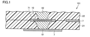
- FIG. 1 shows a partial cross-sectional view of resin multilayer substrate 101 in the present embodiment.
- the resin multilayer substrate 101 includes a first resin layer 21 mainly made of a thermoplastic resin, a second resin layer 22 mainly made of a thermoplastic resin and disposed on the first resin layer 21, and a first resin. Between the first interlayer connection conductor 61 disposed so as to penetrate the layer 21 in the thickness direction, and between the first resin layer 21 and the second resin layer 22, the first interlayer connection conductor 61 includes the first resin layer 21. And a first conductor pattern 71 disposed in a range including a region exposed on the surface. The first conductor pattern 71 includes a first portion 31 disposed so as to cover a region where the first interlayer connecting conductor 61 is exposed on the surface of the first resin layer 21, and a second portion disposed so as to surround the first portion 31. Part 32.
- the first resin layer 21 and the second resin layer 22 contain, for example, a liquid crystal polymer resin.
- the 1st conductor pattern 71 consists of metal foil, for example, copper foil.
- the first interlayer connection conductor 61 is made by solidifying a conductive paste containing Sn, for example.
- the thickness of the first conductor pattern 71 is different between the first portion 31 and the second portion 32.
- FIG. 2 shows an enlarged view of the vicinity of the first conductor pattern 71 shown in FIG.
- T1 ⁇ T2 where T1 is the thickness of the first conductor pattern 71 in the first portion 31, and T2 is the thickness of the first conductor pattern 71 in the second portion 32. This magnitude relationship may be reversed, but in the present embodiment, a case where T1 ⁇ T2 is particularly described below.
- the thickness of the first portion 31 is smaller than the thickness of the second portion 32, and the surface of the first portion 31 on the first resin layer 21 side is the first resin of the second portion 32. Compared to the surface on the layer 21 side, the surface recedes in the thickness direction.
- the portion 10 is not always clogged with only the conductive paste, and the material of the first interlayer connection conductor 61 is not necessarily filled. The material of the first resin layer 21 may enter.
- the first conductor pattern 71 arranged in a range including the region where the first interlayer connecting conductor 61 is exposed on the surface of the first resin layer 21 has the first portion 31 and the second portion 32 having different thicknesses. Therefore, even if the conductive paste constituting the first interlayer connecting conductor 61 contains a low melting point metal such as Sn and part thereof oozes out, the thickness of the first portion 31 and the second portion 32 As a result, the conductive paste accumulates in the stepped portion caused by the difference, and the conductive paste can be prevented from spreading to other undesired portions. Therefore, it is possible to suppress a short circuit failure due to the seepage of the conductive paste.
- the exuded conductive paste accumulates in the portion 10 shown in FIG. Since the portion 10 is surrounded by the second portion 32, the conductive paste that has entered the portion 10 is suppressed from spreading outside the second portion 32.
- the said 1st interlayer connection conductor contains the addition metal which has melting
- the additive metal oozes out in the thermocompression bonding step, but in the present embodiment, a portion having a different thickness is provided in the first conductor pattern 71 to hold the oozed additive metal. Therefore, the effect can be enjoyed particularly remarkably.
- the additive metal is preferably Sn.
- the first interlayer connection conductor can be sufficiently metallized (solidified) in the step of applying pressure while heating to a temperature higher than the softening temperature of the thermoplastic resin. Further, since the exuded Sn can be guided and held in the space formed by the thinned portion of the first conductor pattern 71, the effect can be particularly remarkably enjoyed.
- the first conductor pattern 71 is a copper foil, an intermetallic compound layer such as Cu 6 Sn 5 or a Cu—Sn alloy layer can be formed with Sn as an additive metal. Accordingly, the first conductor pattern 71 and the first interlayer connection conductor 61 can be firmly connected. In addition, since such an intermetallic compound layer or alloy layer is formed, the melting point is increased and it is difficult to flow as compared with a simple substance of Sn, so that it is possible to suppress the seepage of Sn, which is a low melting point metal.
- thermoplastic resin is a liquid crystal polymer resin (also referred to as “LCP resin”).
- LCP resin liquid crystal polymer resin
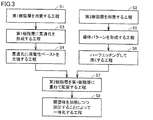
- FIG. 3 shows a flowchart of the method for manufacturing the resin multilayer substrate in the present embodiment.
- the manufacturing method of the resin multilayer substrate in the present embodiment includes a step S1 of preparing a first resin layer mainly made of a thermoplastic resin, and a first method in which a conductor film is arranged on the surface using the thermoplastic resin as a main material.
- step S2 of preparing two resin layers
- step S3 of forming through holes in the first resin layer
- step S4 of filling the through holes with conductive paste
- Step S5 of forming a conductor pattern
- Step S6 of half-etching and thinning one of the outer edge portion of the conductor pattern and the portion surrounded by the outer edge portion
- the surface of the first resin layer A process of placing the second resin layer on the first resin layer so as to cover the region where the through hole is exposed and to arrange the conductor pattern so as to surround the exposed region with the outer edge portion.
- the steps S1 to S6 are shown in this order, but the order of the steps S1 to S6 is not limited to this.
- the timing of performing step S2 may be before step S1, may be after step S4, or may be between step S3 and step S4.
- the timing for performing steps S3 and S4 may be after step S6 or between step S5 and step S6.
- the flow of steps S1, S3, and S4 and the flow of steps S2, S5, and S6 are different. Both may be performed in parallel.
- a resin sheet 12 is arranged on the surface of the PET film 13, and a metal foil is arranged on the surface opposite to the PET film 13 of the resin sheet 12.
- a copper foil 14 is disposed is prepared as an example of a metal foil.
- the resin sheet 12 is mainly made of a thermoplastic resin.
- the thermoplastic resin may be, for example, a liquid crystal polymer resin.
- the copper foil 14 may cover the entire surface of the resin sheet 12.
- the PET film 13 is prepared as a support layer. What remove
- step S5 photolithography is performed on the copper foil 14. As a result, as shown in FIG. 5, only a part of the copper foil 14 is left to form the conductor pattern 7.
- the conductor patterns 7 having various sizes and shapes may be formed, but only the two large and small conductor patterns 7 are shown in FIG. 5 for convenience of explanation.
- step S6 half etching is performed on some of the conductor patterns 7. In other words, etching for partially thinning the conductor pattern 7 is performed. Thereby, as shown in FIG. 6, the 1st conductor pattern 71 is formed. The first conductor pattern 71 is formed as a result of partially removing material from what was originally the conductor pattern 7. In step S6, not all conductor patterns 7 are subject to half etching, and even when half etching is finished, there are other conductor patterns 7 that remain in their original shapes as shown in FIG. Also good.
- the second resin layer 22 shown in FIG. 7 includes a first conductor pattern 71 and a second interlayer connection conductor 62. As shown in FIG. 7, you may provide the conductor pattern 7 which does not contain the part which thickness further became thin partially.
- step S7 the second resin layer 22 is placed over the first resin layer 21.
- a resin layer other than these two resin layers may be stacked together.
- a total of three resin layers are stacked, but the number of resin layers may be two or more and may be other than three.
- FIG. 9 shows a state where they are placed one on top of the other.
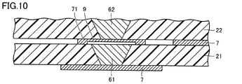
- FIG. 10 shows an enlarged view of the vicinity of the first conductor pattern 71 in the multilayer body 1 shown in FIG. A gap 9 is formed below the first conductor pattern 71.
- the laminate 1 is pressurized while being heated to a temperature equal to or higher than the softening temperature of the thermoplastic resin as step S8.
- the conductive paste that has oozed out from the first interlayer connection conductor 61 enters the lower gap 9 of the first conductor pattern 71.
- the portion 10 is formed on the upper side of the first interlayer connection conductor 61 as shown in FIG.
- the part 10 may be formed of only the conductive paste, but the conductive paste and other materials may be mixed.
- the resin layers are stacked in step S7 in a state where the first conductor pattern 71 included in the second resin layer 22 includes the first portion 31 and the second portion 32 having different thicknesses. Even if the conductive paste constituting the one-layer connection conductor 61 contains a low melting point metal and a part of this conductive paste oozes out in step S8, the difference in thickness between the first portion 31 and the second portion 32. As a result, the conductive paste accumulates in the stepped portion caused by the above. Therefore, it is possible to suppress the conductive paste from spreading to other undesired parts, and it is possible to obtain a resin multilayer substrate while suppressing a short circuit failure due to the seepage of the conductive paste.
- the conductive paste preferably contains an additive metal having a melting point lower than the softening temperature.
- the additive metal oozes out in step S8.
- the first conductor pattern 71 is provided with a portion having a different thickness to hold the oozed additive metal. Therefore, the effect can be enjoyed particularly remarkably.
- FIG. 12 is a partial cross-sectional view of the resin multilayer substrate 102 in the present embodiment.
- the resin multilayer substrate 102 includes a first resin layer 21 mainly made of a thermoplastic resin, a second resin layer 22 made of a thermoplastic resin as a main material and arranged on the first resin layer 21, and a first resin. Between the first interlayer connection conductor 61 disposed so as to penetrate the layer 21 in the thickness direction, and between the first resin layer 21 and the second resin layer 22, the first interlayer connection conductor 61 includes the first resin layer 21. 1st conductor pattern 71i arrange
- the first conductor pattern 71i includes a first portion disposed so as to cover a region where the first interlayer connection conductor 61 is exposed on the surface of the first resin layer 21, and a second portion disposed so as to surround the first portion. including.
- the first portion and the second portion have different thicknesses.
- the thickness of the second portion is smaller than the thickness of the first portion, and the surface of the second portion on the first resin layer 21 side is the surface of the first portion on the first resin layer 21 side. Treatments in the thickness direction compared to the surface.
- the same effect as in the first embodiment can be obtained.
- the exuded conductive paste is more likely to accumulate in the portion 10i shown in FIG. That is, in the step of integrating the laminate by applying pressure while heating to a temperature higher than the softening temperature of the thermoplastic resin of the first resin layer 21 and the second resin layer 22, other conductors around the first conductor pattern 71i. It becomes easy to fill a gap between the resin layers between the patterns. Thereby, it is suppressed that the electrically conductive paste which entered the part 10i spreads outside.
- FIG. 13 to FIG. 17 a method for manufacturing a resin multilayer substrate according to the second embodiment of the present invention will be described. Reference is again made to FIGS. 3, 4, and 12. This manufacturing method is for obtaining the resin multilayer substrate 102.
- the manufacturing method of the resin multilayer substrate in the present embodiment is a manufacturing method within the range of the flowchart shown in FIG.
- step S ⁇ b> 2 a resin sheet 12 is arranged on the surface of the PET film 13 and a copper foil 14 is arranged on the surface opposite to the PET film 13 of the resin sheet 12. Is the same as described in the first embodiment.
- the first conductor pattern 71 i is formed as a result of partial removal of what was originally the conductor pattern 7.
- a through-hole is formed from the state shown in FIG. 13 by laser processing, the conductive paste is filled in the through-hole, and the PET film 13 is peeled off to obtain the structure shown in FIG.
- the second resin layer 22 shown in FIG. 14 includes a first conductor pattern 71 i and a second interlayer connection conductor 62. Furthermore, you may provide the conductor pattern 7 which does not include the part where thickness became thin partially.
- step S7 the second resin layer 22 is disposed so as to overlap the first resin layer 21.
- a resin layer other than these two resin layers may be stacked together.
- FIG. 16 shows a state where they are placed one on top of the other.
- FIG. 17 shows an enlarged view of the vicinity of the first conductor pattern 71i when the laminate is further pressurized. A gap 9 is formed below the outer edge of the first conductor pattern 71i.
- the laminate 1 is pressurized while being heated to a temperature equal to or higher than the softening temperature of the thermoplastic resin as step S8.
- the conductive paste that has exuded from the first interlayer connection conductor 61 enters the lower gap 9 of the first conductor pattern 71i.
- a portion 10 i is formed below the first interlayer connection conductor 61 as shown in FIG.
- the part 10i may be formed of only the conductive paste, but the conductive paste and other materials may be mixed.
- a step is formed on the entire outer periphery of the first conductor pattern 71i.
- the short-circuit defect between adjacent conductors on the outer periphery of the first conductor pattern is a problem.
- step difference only in may be sufficient.
- the thinned second portion may be formed on the outer periphery of the first conductor pattern only at a location where the distance to the adjacent conductor is set to be shorter than a certain distance.
- the second portion may be formed on only a part of the outer periphery of one first conductor pattern.
- FIG. 3 A cross-sectional view of the resin multilayer substrate 103 in the present embodiment is shown in FIG.
- the resin multilayer substrate 103 includes a first resin layer 21 mainly made of a thermoplastic resin, a second resin layer 22 made of the thermoplastic resin as a main material and arranged on the first resin layer 21, and a first resin layer 21. Between the first interlayer connection conductor 61 disposed so as to penetrate the resin layer 21 in the thickness direction, and between the first resin layer 21 and the second resin layer 22, the first interlayer connection conductor 61 is the first resin layer 21. And a first conductor pattern 71 disposed in a range including a region exposed on the surface of the first conductor pattern 71. The first conductor pattern 71 includes a portion that accommodates a part of the first interlayer connection conductor 61. In the present embodiment, as shown in FIG. 18, a recess is provided in the first conductor pattern 71, and a part near the upper end of the first interlayer connecting conductor 61 is accommodated in this recess.
- the first conductor pattern 71 only a part of the low melting point metal contained in the conductive paste constituting the first interlayer connection conductor 61 may be accommodated in the first conductor pattern 71.
- what is accommodated in the first interlayer connection conductor 61 is not limited to a specific component included in the conductive paste, and as shown in the present embodiment, the conductive paste constituting the first interlayer connection conductor 61. Among them, a part close to the first conductor pattern 71 may be accommodated as it is.
- the effect described in the first embodiment can be obtained.
- the first conductor pattern 71 includes a portion that accommodates the first interlayer connection conductor 61, a part of the first interlayer connection conductor 61 is accommodated here, so that the first interlayer connection The total dimension in the thickness direction of the conductor 61 and the first conductor pattern 71 can be reduced. Therefore, it can reduce that the site
- a recess is provided on the lower surface of the conductor pattern, and a part near the upper end of the interlayer connection conductor in contact with the conductor pattern from the lower side enters the recess. May be reversed. That is, a recess may be provided on the upper surface of the conductor pattern, and a portion near the lower end of the interlayer connection conductor that is in contact with the conductor pattern from above may enter the recess.
- the resin multilayer substrate 103 includes a series connection portion that is a portion in which a larger number of interlayer connection conductors are overlapped with each other in the other portions in the resin multilayer substrate 103, and
- the conductor pattern 71 is preferably included in the series connection portion.
- four groups are shown in the left-right direction, and the second group from the right corresponds to the series connection unit.
- the series connection portion which is a portion where a large number of interlayer connection conductors are overlapped with each other compared to other parts, there is a concern that a convex portion is generated on the outermost surface of the resin multilayer substrate.
- the 1st conductor pattern is contained in the serial connection part, the problem that a convex part arises can be suppressed effectively. The same applies to the other embodiments described below.
- the resin multilayer substrate 103 is basically manufactured by stacking a plurality of resin layers 2, but for convenience of explanation, a specific one of the plurality of resin layers 2 is a first resin layer 21, Another specific one layer will be described as the second resin layer 22. Both the first resin layer 21 and the second resin layer 22 are a kind of the resin layer 2.
- the copper foil on the surface of each resin layer 2 is patterned to form a conductor pattern.
- a portion having a reduced thickness is formed by a method such as half etching.
- the through hole 15 is formed by laser processing or the like.
- the conductor pattern is formed first, the order is not limited to this, and either the formation of the conductor pattern or the formation of the through hole 15 may be performed first.
- FIG. 20 each through-hole 15 of each resin layer 2 is filled with a conductor paste that becomes an interlayer connection conductor.
- the first interlayer connection conductor 61 is formed on the first resin layer 21, and the second interlayer connection conductor 62 is formed on the second resin layer 22.
- the resin multilayer substrate 103 shown in FIG. 18 can be obtained.
- Embodiment 4 With reference to FIG. 21, a resin multilayer substrate according to Embodiment 4 of the present invention will be described. A cross-sectional view of the resin multilayer substrate 104 in this embodiment is shown in FIG.
- the resin multilayer substrate 104 includes a first conductor pattern 71j.
- the first conductor pattern 71j is a conductor pattern through-hole that is a through-hole disposed so as to at least partially overlap a region where the first interlayer connection conductor 61 is exposed on the surface of the first resin layer 21. 16 is included.
- the conductor pattern through hole 16 may partially overlap the first interlayer connection conductor 61, but the conductor pattern through hole 16 may entirely overlap the first interlayer connection conductor 61.
- the conductor pattern through hole 16 is provided in the first conductor pattern 71j, and at least a part of the conductor pattern through hole 16 is exposed to the first interlayer connection conductor 61 on the surface of the first resin layer 21. Since the first interlayer connection conductor 61 is partly accommodated in the conductor pattern through hole 16, the dimension in the thickness direction can be reduced. Therefore, it can reduce that the site
- This manufacturing method is for obtaining the resin multilayer substrate 104 (see FIG. 21).
- the copper foil on the surface is patterned in each resin layer 2 to form a conductor pattern.
- a conductor pattern through hole 16 is formed.
- the conductor pattern through-hole 16 can be formed by a known technique such as laser processing.
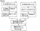
- FIG. 23 shows a flowchart of the method for manufacturing the resin multilayer substrate in the present embodiment.
- the method for producing a resin multilayer substrate includes a step S1 of preparing a first resin layer mainly composed of a thermoplastic resin, and a second resin layer having the thermoplastic resin as a main material and a conductor film disposed on the surface. Patterning the conductive film of the second resin layer, step S2 of forming a first through hole in the first resin layer, step S14 of filling the first through hole with a conductive paste, Step S5 of forming a conductor pattern, Step S16 of forming a second through hole in the conductor pattern, and a region where the first through hole is exposed on the surface of the first resin layer, and covering the exposed region.
- the through hole 15 formed in the resin layer 2 corresponds to the “first through hole”
- the conductor pattern through hole 16 formed in the first conductor pattern 71j is “ It corresponds to a “second through hole”.
Landscapes
- Engineering & Computer Science (AREA)
- Microelectronics & Electronic Packaging (AREA)
- Manufacturing & Machinery (AREA)
- Chemical & Material Sciences (AREA)
- Dispersion Chemistry (AREA)
- Production Of Multi-Layered Print Wiring Board (AREA)
Abstract
樹脂多層基板(101)は、熱可塑性樹脂を主材料とする第1樹脂層(21)と、前記熱可塑性樹脂を主材料とし、第1樹脂層(21)に重ねて配置された第2樹脂層(22)と、第1樹脂層(21)を厚み方向に貫通するように配置された第1層間接続導体(61)と、第1樹脂層(21)と第2樹脂層(22)との間において、第1層間接続導体(61)が第1樹脂層(21)の表面に露出する領域を含む範囲に配置された第1導体パターン(71)とを備える。第1導体パターン(71)は、第1層間接続導体(61)の一部を収容する部分を含む。たとえば第1導体パターン(71)は、第1樹脂層(21)の表面に露出する領域を覆うように配置された第1部分と前記第1部分を取り囲むように配置された第2部分とを含み、前記第1部分と前記第2部分とで厚みが異なる。
Description
本発明は、樹脂多層基板およびその製造方法に関するものである。
国際公開WO2012/111711号(特許文献1)には、導体箔からなる導体配線層が表面に形成され、熱可塑性樹脂を含む樹脂シートを積層して作製された多層配線基板が記載されている。この多層配線基板の内部のビアホール導体は、Snなどを含む導電性ペーストによって形成されている。
特許文献1に記載された多層配線基板は、樹脂シートを積層して作製されたものであるので、樹脂多層基板に該当する。樹脂多層基板においては、厚み方向に離れた位置にある導体パターン同士を電気的に接続する際に層間接続導体が用いられる。層間接続導体の元となる導電性ペーストは、Snなどの低融点金属を含む場合がある。Snなどの低融点金属を含む導電性ペーストを用いた場合、積層した複数の樹脂シートを圧着させるために加熱および加圧を加える際に、層間接続導体となるべき導電性ペーストの部分から低融点金属が染み出して樹脂層同士の隙間に広がる。その結果、染み出た低融点金属が不所望な導体パターン同士の間を導通させてしまい、ショート不良をもたらすという問題が生じる。
特に隣接する異なる電位の導体パターン間の距離が短い場合、そのような染み出した金属によるショート不良は発生しやすい。一方、染み出しを避けるために導電性ペーストにはSnなどの低融点金属を添加しないこととすれば、熱可塑性樹脂を含む複数の樹脂シートを積層して熱可塑性樹脂の軟化温度以上に加熱しつつ加圧する工程において層間接続導体が金属化しにくくなる。
そこで、本発明は、層間接続導体となるべき導電性ペーストの染み出しによるショート不良を抑制することができる樹脂多層基板およびその製造方法を提供することを目的とする。
上記目的を達成するため、本発明に基づく樹脂多層基板は、熱可塑性樹脂を主材料とする第1樹脂層と、上記熱可塑性樹脂を主材料とし、上記第1樹脂層に重ねて配置された第2樹脂層と、上記第1樹脂層を厚み方向に貫通するように配置された第1層間接続導体と、上記第1樹脂層と上記第2樹脂層との間において、上記第1層間接続導体が上記第1樹脂層の表面に露出する領域を含む範囲に配置された第1導体パターンとを備え、上記第1導体パターンは、上記第1層間接続導体の一部を収容する部分を含む。
本発明によれば、第1層間接続導体の一部が第1導体パターンによって収容されることとなり、他の不所望な部位に導電性ペーストが広がることを抑制することができる。したがって、導電性ペーストの染み出しによるショート不良を抑制することができる。
図面において示す寸法比は、必ずしも忠実に現実のとおりを表しているとは限らず、説明の便宜のために寸法比を誇張して示している場合がある。以下の説明において、上または下の概念に言及する際には、絶対的な上または下を意味するとは限らず、図示された姿勢の中での相対的な上または下を意味する場合がある。
(実施の形態1)
図1および図2を参照して、本発明に基づく実施の形態1における樹脂多層基板について説明する。本実施の形態における樹脂多層基板101の部分断面図を図1に示す。
図1および図2を参照して、本発明に基づく実施の形態1における樹脂多層基板について説明する。本実施の形態における樹脂多層基板101の部分断面図を図1に示す。
樹脂多層基板101は、熱可塑性樹脂を主材料とする第1樹脂層21と、熱可塑性樹脂を主材料とし、第1樹脂層21に重ねて配置された第2樹脂層22と、第1樹脂層21を厚み方向に貫通するように配置された第1層間接続導体61と、第1樹脂層21と第2樹脂層22との間において、第1層間接続導体61が第1樹脂層21の表面に露出する領域を含む範囲に配置された第1導体パターン71とを備える。第1導体パターン71は、第1層間接続導体61が第1樹脂層21の表面に露出する領域を覆うように配置された第1部分31と第1部分31を取り囲むように配置された第2部分32とを含む。第1樹脂層21および第2樹脂層22は、たとえば液晶ポリマー樹脂を含むものである。また、第1導体パターン71は、金属箔、たとえば銅箔からなる。また、第1層間接続導体61は、たとえばSnを含む導電性ペーストが固化したものである。第1部分31と第2部分32とで第1導体パターン71の厚みが異なる。図1に示した第1導体パターン71の近傍を拡大して図2に示す。図1および図2に示した例では、第1部分31における第1導体パターン71の厚みをT1とし、第2部分32における第1導体パターン71の厚みをT2とすると、T1<T2である。この大小関係は逆であってもよいが、本実施の形態では、特にT1<T2である場合について以下説明する。
本実施の形態では、第1部分31の厚みは第2部分32の厚みに比べて薄くなっており、第1部分31の第1樹脂層21側の表面は、第2部分32の第1樹脂層21側の表面に比べて厚み方向に後退している。第1部分31の下側に部位10がある。部位10には第1層間接続導体61を構成する導電性ペーストの一部が溜まっている。ここでは模式的に導電性ペーストのみが溜まっているように図示しているが、実際には、部位10には導電性ペーストのみが詰まっているとは限らず、第1層間接続導体61の材料、第1樹脂層21の材料が進入していてもよい。
本実施の形態では、第1層間接続導体61が第1樹脂層21の表面に露出する領域を含む範囲に配置された第1導体パターン71が厚みの異なる第1部分31と第2部分32とを備えるので、たとえ第1層間接続導体61を構成する導電性ペーストがSnなどの低融点金属を含んでいてその一部が染み出したとしても、第1部分31と第2部分32との厚みの差によって生じた段差部分に導電性ペーストが溜まることとなり、他の不所望な部位に導電性ペーストが広がることを抑制することができる。したがって、導電性ペーストの染み出しによるショート不良を抑制することができる。
本実施の形態では、第2部分32よりも第1部分31の方が薄くなっているので、染み出した導電性ペーストは図1に示す部位10に溜まることとなる。部位10は周囲を第2部分32によって囲まれているので、部位10に入り込んだ導電性ペーストは第2部分32より外側に広がることが抑制される。
なお、第1樹脂層21の主材料である熱可塑性樹脂の軟化温度よりも低い融点を有する添加金属が前記第1層間接続導体に含まれていることが好ましい。このような場合、熱圧着の工程において添加金属の染み出しが起こる可能性が高いが、本実施の形態では、第1導体パターン71に厚みの異なる部分を設け、染み出した添加金属を保持することができるので、特に顕著に効果を享受することができる。
添加金属はSnであることが好ましい。この構成を採用することにより、熱可塑性樹脂の軟化温度以上に加熱しつつ加圧する工程において、十分に第1層間接続導体を金属化(固化)させやすくなる。また、染み出したSnを第1導体パターン71に厚みが薄くなった部分によって形成された空間に導き、保持することができるので、特に顕著に効果を享受することができる。また、第1導体パターン71が銅箔である場合、添加金属であるSnとの間で、Cu6Sn5のような金属間化合物層やCu-Sn合金層を形成させることができる。これにより、第1導体パターン71と第1層間接続導体61との間を強固に接続できる。また、このような金属間化合物層や合金層が形成されることによりSn単体と比較して融点が上がり流動しにくくなるので、低融点金属であるSnの染み出しを抑制することができる。
前記熱可塑性樹脂は液晶ポリマー樹脂(「LCP樹脂」ともいう。)であることが好ましい。この構成を採用することにより、高周波特性に優れた樹脂多層基板を得ることができる。
図3~図11を参照して、本発明に基づく実施の形態1における樹脂多層基板の製造方法について説明する。本実施の形態における樹脂多層基板の製造方法のフローチャートを図3に示す。
本実施の形態における樹脂多層基板の製造方法は、熱可塑性樹脂を主材料とする第1樹脂層を用意する工程S1と、前記熱可塑性樹脂を主材料とし、表面に導体膜が配置された第2樹脂層を用意する工程S2と、前記第1樹脂層に貫通孔を形成する工程S3と、前記貫通孔に導電性ペーストを充填する工程S4と、前記第2樹脂層の導体膜をパターニングして導体パターンを形成する工程S5と、前記導体パターンの外縁部および前記外縁部に取り囲まれた部分のうちいずれか一方をハーフエッチングして薄くする工程S6と、前記第1樹脂層の表面のうち前記貫通孔が露出する領域を覆い、前記露出する領域を前記外縁部を以て取り囲むように前記導体パターンが配置されるように、前記第2樹脂層を前記第1樹脂層に重ねて配置する工程S7と、前記第1樹脂層および前記第2樹脂層を含む積層体を、前記熱可塑性樹脂の軟化温度以上に加熱しつつ加圧することによって一体化する工程S8とを含む。
ここでは説明の便宜上、工程S1~S6をこの順に示したが、工程S1~S6の順序はこのとおりとは限らない。たとえば工程S2を行なうタイミングは工程S1より前であってもよく、工程S4の後であってもよく、工程S3と工程S4との間であってもよい。たとえば工程S3,S4を行なうタイミングは、工程S6の後であってもよく、工程S5と工程S6との間であってもよい。図3にフローチャートに示したように、工程S1,S3,S4の流れと、工程S2,S5,S6の流れとは別ものであるので、一方を先に行なった後に他方を行なってもよく、両方を並行して行なってもよい。
以下では、いくつかの工程の具体的な様子について、説明する。ここでは、樹脂多層基板101を得る場合を例にとって説明する。実際には、この製造方法で製造する対象は、樹脂多層基板101に限らない。
工程S2として、図4に示すように、PETフィルム13の表面に樹脂シート12が配置され、樹脂シート12のPETフィルム13とは逆側の表面に金属箔が配置されたものを用意する。本実施の形態では、金属箔の一例として銅箔14が配置されたものを用意する。樹脂シート12は熱可塑性樹脂を主材料としたものである。熱可塑性樹脂とはたとえば液晶ポリマー樹脂であってよい。銅箔14は、樹脂シート12の全面を覆っていてよい。PETフィルム13は、支持層として用意されたものである。ここで用意されたものからPETフィルム13を除いたものが第2樹脂層22である。
工程S5として、銅箔14に対してフォトリソグラフィを行なう。その結果、図5に示すように、銅箔14の一部のみが残されて導体パターン7となる。ここでは、さまざまなサイズ、形状の導体パターン7が形成されてもよいが、図5では説明の便宜のために大小2つの導体パターン7のみを示している。
工程S6として、一部の導体パターン7に対してハーフエッチングを行なう。言い換えれば、導体パターン7を部分的に薄くするエッチングを行なう。これにより、図6に示すように、第1導体パターン71が形成される。第1導体パターン71は、元は導体パターン7であったものから材料を部分的に除去した結果として形成されたものである。工程S6では、全ての導体パターン7がハーフエッチングの対象となるとは限らず、ハーフエッチングが終わった時点でも、図6に示すように、元の形状のままの導体パターン7が他に存在してもよい。
図6に示した状態からレーザ加工などによって貫通孔を形成し、貫通孔に導電性ペーストを充填し、PETフィルム13を剥離することによって、図7に示す構造が得られる。図7に示す第2樹脂層22は、第1導体パターン71と、第2層間接続導体62とを備える。図7に示すようにさらに厚みが部分的に薄くなった部分を含まない導体パターン7を備えていてもよい。
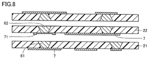
工程S7として、図8に示すように、第2樹脂層22を第1樹脂層21に重ねて配置する。このとき、これら2つの樹脂層以外の樹脂層も併せて重ねてもよい。図8では、合計3層の樹脂層が積み重ねられているが、樹脂層の数は2層以上であればよく、3層以外であってもよい。重ねて置いた状態を図9に示す。図9に示した積層体1のうち第1導体パターン71の近傍を拡大したところを図10に示す。第1導体パターン71の下側に間隙9が生じている。
積層体1に対して、工程S8として、熱可塑性樹脂の軟化温度以上に加熱しつつ加圧する。このとき、第1層間接続導体61から染み出た導電性ペーストが第1導体パターン71の下側の間隙9に入り込む。その結果、図11に示すように第1層間接続導体61の上側に部位10が形成される。部位10は導電性ペーストのみで形成されていてもよいが、導電性ペーストと他の材料とが混在してもよい。
本実施の形態では、第2樹脂層22が備える第1導体パターン71が厚みの異なる第1部分31と第2部分32とを備える状態で工程S7で各樹脂層が積み重ねられたので、たとえ第1層間接続導体61を構成する導電性ペーストが低融点金属を含んでいて工程S8においてこの導電性ペーストの一部が染み出したとしても、第1部分31と第2部分32との厚みの差によって生じた段差部分に導電性ペーストが溜まることとなる。したがって、他の不所望な部位に導電性ペーストが広がることを抑制することができ、導電性ペーストの染み出しによるショート不良を抑制しつつ、樹脂多層基板を得ることができる。
本実施の形態における樹脂多層基板の製造方法で、導電性ペーストは、前記軟化温度より低い融点を有する添加金属を含むことが好ましい。このような場合、工程S8において添加金属の染み出しが起こる可能性が高いが、本実施の形態では、第1導体パターン71に厚みの異なる部分を設け、染み出した添加金属を保持することができるので、特に顕著に効果を享受することができる。
(実施の形態2)
図12を参照して、本発明に基づく実施の形態2における樹脂多層基板について説明する。本実施の形態における樹脂多層基板102の部分断面図を図12に示す。
図12を参照して、本発明に基づく実施の形態2における樹脂多層基板について説明する。本実施の形態における樹脂多層基板102の部分断面図を図12に示す。
樹脂多層基板102は、熱可塑性樹脂を主材料とする第1樹脂層21と、熱可塑性樹脂を主材料とし、第1樹脂層21に重ねて配置された第2樹脂層22と、第1樹脂層21を厚み方向に貫通するように配置された第1層間接続導体61と、第1樹脂層21と第2樹脂層22との間において、第1層間接続導体61が第1樹脂層21の表面に露出する領域を含む範囲に配置された第1導体パターン71iとを備える。第1導体パターン71iは、第1層間接続導体61が第1樹脂層21の表面に露出する領域を覆うように配置された第1部分と第1部分を取り囲むように配置された第2部分とを含む。第1部分と第2部分とで厚みが異なる。
本実施の形態では、第2部分の厚みは第1部分の厚みに比べて薄くなっており、第2部分の第1樹脂層21側の表面は、第1部分の第1樹脂層21側の表面に比べて厚み方向に後退している。
本実施の形態においても、実施の形態1と同様の効果を得ることができる。ただし、本実施の形態では、第1部分よりもその周りの第2部分の方が薄くなっているので、染み出した導電性ペーストは図12に示す部位10iにさらに溜まりやすくなる。すなわち、第1樹脂層21および第2樹脂層22の熱可塑性樹脂の軟化温度以上に加熱しつつ加圧することによって積層体を一体化する工程において、第1導体パターン71iの周辺にある他の導体パターンとの間の樹脂層間の隙間を埋めやすくなる。これにより、部位10iに入り込んだ導電性ペーストは外側に広がることが抑制される。
図13~図17を参照して、本発明に基づく実施の形態2における樹脂多層基板の製造方法について説明する。図3、図4、図12も再び参照する。この製造方法は、樹脂多層基板102を得るためのものである。本実施の形態における樹脂多層基板の製造方法は、図3に示したフローチャートの範囲内の製造方法である。
工程S2として、図4に示すように、PETフィルム13の表面に樹脂シート12が配置され、樹脂シート12のPETフィルム13とは逆側の表面に銅箔14が配置されたものを用意する点は、実施の形態1で述べたのと同じである。
工程S5,S6を行なうことによって、図13に示す構造を得る。第1導体パターン71iは、元は導体パターン7であったものを部分的に除去した結果として形成されたものである。図13に示した状態からレーザ加工などによって貫通孔を形成し、貫通孔に導電性ペーストを充填し、PETフィルム13を剥離することによって、図14に示す構造が得られる。図14に示す第2樹脂層22は、第1導体パターン71iと、第2層間接続導体62とを備える。さらに厚みが部分的に薄くなった部分を含まない導体パターン7を備えていてもよい。
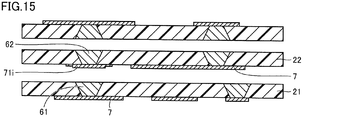
工程S7として、図15に示すように、第2樹脂層22を第1樹脂層21に重ねて配置する。このとき、これら2つの樹脂層以外の樹脂層も併せて重ねてもよい。重ねて置いた状態を図16に示す。この積層体をさらに加圧したときの、第1導体パターン71iの近傍を拡大したところを図17に示す。第1導体パターン71iの外縁部の下側に間隙9が生じている。
積層体1に対して、工程S8として、熱可塑性樹脂の軟化温度以上に加熱しつつ加圧する。このとき、第1層間接続導体61から染み出た導電性ペーストが第1導体パターン71iの下側の間隙9に入り込む。その結果、図12に示すように第1層間接続導体61の下側に部位10iが形成される。部位10iは導電性ペーストのみで形成されていてもよいが、導電性ペーストと他の材料とが混在してもよい。
本実施の形態では、第1導体パターン71iの外周の全体に段差が形成されたものを示したが、第1導体パターンの外周のうち隣りの導電体との間のショート不良が問題になる箇所のみにおいて段差を形成した構成であってもよい。すなわち、隣の導電体との距離が一定以上短く設定されている箇所のみにおいて第1導体パターンの外周に薄くなった第2部分を形成してもよい。1つの第1導体パターンの外周のうち一部のみに第2部分が形成されていてもよい。
(実施の形態3)
図18を参照して、本発明に基づく実施の形態3における樹脂多層基板について説明する。本実施の形態における樹脂多層基板103の断面図を図18に示す。
図18を参照して、本発明に基づく実施の形態3における樹脂多層基板について説明する。本実施の形態における樹脂多層基板103の断面図を図18に示す。
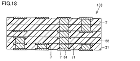
樹脂多層基板103は、熱可塑性樹脂を主材料とする第1樹脂層21と、前記熱可塑性樹脂を主材料とし、第1樹脂層21に重ねて配置された第2樹脂層22と、第1樹脂層21を厚み方向に貫通するように配置された第1層間接続導体61と、第1樹脂層21と第2樹脂層22との間において、第1層間接続導体61が第1樹脂層21の表面に露出する領域を含む範囲に配置された第1導体パターン71とを備える。第1導体パターン71は、第1層間接続導体61の一部を収容する部分を含む。本実施の形態では、図18に示すように、第1導体パターン71に凹部が設けられており、この凹部に第1層間接続導体61の上端近傍の一部が入り込むことによって収容されている。
第1導体パターン71に収容されるのは、実施の形態1で説明したように、第1層間接続導体61を構成する導電性ペーストに含まれる低融点金属の一部のみであってもよいが、第1層間接続導体61に収容されるものは導電性ペーストに含まれる特定の成分のみとは限らず、本実施の形態で示したように、第1層間接続導体61を構成する導電性ペーストのうち第1導体パターン71に近い位置にある一部がそのまま収容されてもよい。
本実施の形態においても、実施の形態1で説明した効果を得ることができる。さらに本実施の形態では、第1導体パターン71は、第1層間接続導体61を収容する部分を含むので、第1層間接続導体61の一部がここに収容されることで、第1層間接続導体61と第1導体パターン71との合計の厚み方向の寸法を減らすことができている。したがって、樹脂多層基板の最表面において第1層間接続導体61に対応する部位が局所的に凸部となることを軽減することができる。
本実施の形態では、導体パターンの下面に凹部が設けられており、この導体パターンに対して下側から接する層間接続導体の上端近傍の一部がこの凹部に入り込むものとして説明したが、上下関係は逆であってもよい。すなわち、導体パターンの上面に凹部が設けられており、この導体パターンに対して上側から接する層間接続導体の下端近傍の一部がこの凹部に入り込むものであってもよい。
図18に示したように、樹脂多層基板103は、樹脂多層基板103内の他の部位に比べて多くの数の層間接続導体が重なって配置された部分である直列接続部を備え、第1導体パターン71は、前記直列接続部に含まれていることが好ましい。図18に示した例では、左右方向に4つの群が示されているが、そのうち右から2番目の群が直列接続部に該当する。このように、他の部位に比べて多くの数の層間接続導体が重なって配置された部分である直列接続部においては、樹脂多層基板の最表面に凸部が生じることが懸念されるが、本実施の形態では、直列接続部に第1導体パターンが含まれているので、凸部が生じるという問題を効果的に抑制することができる。以下に説明する他の実施の形態においても同様のことがいえる。
図19~図20を参照して、本発明に基づく実施の形態3における樹脂多層基板の製造方法について説明する。この製造方法は、樹脂多層基板103(図18参照)を得るためのものである。樹脂多層基板103は、基本的に複数の樹脂層2を積み重ねて作製するものであるが、説明の便宜のため、複数の樹脂層2のうちの特定の1層を第1樹脂層21とし、別の特定の1層を第2樹脂層22として説明する。第1樹脂層21も第2樹脂層22も樹脂層2の一種である。
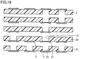
本実施の形態における樹脂多層基板の製造方法では、図19に示すように、各樹脂層2において表面の銅箔をパターニングし、導体パターンを形成する。一部の導体パターンにおいては、ハーフエッチングなどの方法により厚みを薄くした部分を形成する。さらにレーザ加工などによって貫通孔15を形成する。ここでは、導体パターンの形成を先に行なうものとして説明したが、順序はこれに限らず、導体パターンの形成と貫通孔15の形成とはいずれを先に行なってもよい。次に、図20に示すように、各樹脂層2の各貫通孔15に層間接続導体となる導体ペーストを充填する。図20では、第1樹脂層21に第1層間接続導体61が形成され、第2樹脂層22に第2層間接続導体62が形成されている。これらの樹脂層を積み重ねて加熱および加圧を行なうことにより、図18に示した樹脂多層基板103を得ることができる。
本実施の形態では、導電性ペーストの染み出しによるショート不良を抑制しつつ、表面の局所的な凸部の発生を防いで平坦度に優れた樹脂多層基板を得ることができる。
(実施の形態4)
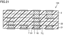
図21を参照して、本発明に基づく実施の形態4における樹脂多層基板について説明する。本実施の形態における樹脂多層基板104の断面図を図21に示す。樹脂多層基板104は第1導体パターン71jを備える。
図21を参照して、本発明に基づく実施の形態4における樹脂多層基板について説明する。本実施の形態における樹脂多層基板104の断面図を図21に示す。樹脂多層基板104は第1導体パターン71jを備える。
本実施の形態では、第1導体パターン71jは、第1層間接続導体61が第1樹脂層21の表面に露出する領域に少なくとも一部が重なるように配置された貫通孔である導体パターン貫通孔16を含む。導体パターン貫通孔16の一部が第1層間接続導体61に重なる構成であってもよいが、導体パターン貫通孔16の全体が第1層間接続導体61に重なる構成であってもよい。
本実施の形態では、第1導体パターン71jに導体パターン貫通孔16が設けられており、導体パターン貫通孔16の少なくとも一部は、第1層間接続導体61が第1樹脂層21の表面に露出する領域に重なっているので、第1層間接続導体61の一部が導体パターン貫通孔16の内部に収容されることで、厚み方向の寸法を減らすことができている。したがって、樹脂多層基板の最表面において第1層間接続導体61に対応する部位が局所的に凸部となることを軽減することができる。
図22~図23を参照して、本発明に基づく実施の形態4における樹脂多層基板の製造方法について説明する。この製造方法は、樹脂多層基板104(図21参照)を得るためのものである。
本実施の形態における樹脂多層基板の製造方法では、図22に示すように、各樹脂層2において表面の銅箔をパターニングし、導体パターンを形成する。一部の導体パターンにおいては、導体パターン貫通孔16を形成する。導体パターン貫通孔16は、レーザ加工などの公知技術により形成することができる。
本実施の形態における樹脂多層基板の製造方法のフローチャートを図23に示す。
樹脂多層基板の製造方法は、熱可塑性樹脂を主材料とする第1樹脂層を用意する工程S1と、上記熱可塑性樹脂を主材料と、表面に導体膜が配置された第2樹脂層を用意する工程S2と、上記第1樹脂層に第1貫通孔を形成する工程S13と、上記第1貫通孔に導電性ペーストを充填する工程S14と、上記第2樹脂層の導体膜をパターニングして導体パターンを形成する工程S5と、上記導体パターンに第2貫通孔を形成する工程S16と、上記第1樹脂層の表面のうち上記第1貫通孔が露出する領域を覆い、上記露出する領域に上記第2貫通孔の少なくとも一部が重なるように上記導体パターンが配置されるように、上記第2樹脂層を上記第1樹脂層に重ねて配置する工程S7と、上記第1樹脂層および上記第2樹脂層を含む積層体を、上記熱可塑性樹脂の軟化温度以上に加熱しつつ加圧することによって一体化する工程S8とを含む。図21~図22に示した例でいえば、樹脂層2に形成された貫通孔15が「第1貫通孔」に相当し、第1導体パターン71jに形成された導体パターン貫通孔16が「第2貫通孔」に相当する。
樹脂多層基板の製造方法は、熱可塑性樹脂を主材料とする第1樹脂層を用意する工程S1と、上記熱可塑性樹脂を主材料と、表面に導体膜が配置された第2樹脂層を用意する工程S2と、上記第1樹脂層に第1貫通孔を形成する工程S13と、上記第1貫通孔に導電性ペーストを充填する工程S14と、上記第2樹脂層の導体膜をパターニングして導体パターンを形成する工程S5と、上記導体パターンに第2貫通孔を形成する工程S16と、上記第1樹脂層の表面のうち上記第1貫通孔が露出する領域を覆い、上記露出する領域に上記第2貫通孔の少なくとも一部が重なるように上記導体パターンが配置されるように、上記第2樹脂層を上記第1樹脂層に重ねて配置する工程S7と、上記第1樹脂層および上記第2樹脂層を含む積層体を、上記熱可塑性樹脂の軟化温度以上に加熱しつつ加圧することによって一体化する工程S8とを含む。図21~図22に示した例でいえば、樹脂層2に形成された貫通孔15が「第1貫通孔」に相当し、第1導体パターン71jに形成された導体パターン貫通孔16が「第2貫通孔」に相当する。
本実施の形態では、導電性ペーストの染み出しによるショート不良を抑制しつつ、表面の局所的な凸部の発生を防いで平坦度に優れた樹脂多層基板を得ることができる。
なお、上記実施の形態のうち複数を適宜組み合わせて採用してもよい。
なお、今回開示した上記実施の形態はすべての点で例示であって制限的なものではない。本発明の範囲は請求の範囲によって示され、請求の範囲と均等の意味および範囲内でのすべての変更を含むものである。
なお、今回開示した上記実施の形態はすべての点で例示であって制限的なものではない。本発明の範囲は請求の範囲によって示され、請求の範囲と均等の意味および範囲内でのすべての変更を含むものである。
1 積層体、2 樹脂層、7 導体パターン、9 間隙、10,10i 部位、12 樹脂シート、13 PETフィルム、14 銅箔、15 貫通孔、16 導体パターン貫通孔、21 第1樹脂層、22 第2樹脂層、31 第1部分、32 第2部分、61 第1層間接続導体、62 第2層間接続導体、71,71i,71j 第1導体パターン、101,102,103,104 樹脂多層基板。
Claims (12)
- 熱可塑性樹脂を主材料とする第1樹脂層と、
前記熱可塑性樹脂を主材料とし、前記第1樹脂層に重ねて配置された第2樹脂層と、
前記第1樹脂層を厚み方向に貫通するように配置された第1層間接続導体と、
前記第1樹脂層と前記第2樹脂層との間において、前記第1層間接続導体が前記第1樹脂層の表面に露出する領域を含む範囲に配置された第1導体パターンとを備え、
前記第1導体パターンは、前記第1層間接続導体の一部を収容する部分を含む、樹脂多層基板。 - 前記第1導体パターンは、前記第1層間接続導体が前記第1樹脂層の表面に露出する領域を覆うように配置された第1部分と前記第1部分を取り囲むように配置された第2部分とを含み、前記第1部分と前記第2部分とで厚みが異なる、請求項1に記載の樹脂多層基板。
- 前記第1部分の厚みは前記第2部分の厚みに比べて薄くなっており、前記第1部分の前記第1樹脂層側の表面は、前記第2部分の前記第1樹脂層側の表面に比べて厚み方向に後退している、請求項2に記載の樹脂多層基板。
- 前記第2部分の厚みは前記第1部分の厚みに比べて薄くなっており、前記第2部分の前記第1樹脂層側の表面は、前記第1部分の前記第1樹脂層側の表面に比べて厚み方向に後退している、請求項2に記載の樹脂多層基板。
- 前記第1導体パターンは、前記第1層間接続導体が前記第1樹脂層の表面に露出する領域に少なくとも一部が重なるように配置された貫通孔である導体パターン貫通孔を含む、請求項1に記載の樹脂多層基板。
- 前記熱可塑性樹脂の軟化温度よりも低い融点を有する添加金属が前記第1層間接続導体に含まれている、請求項1から5のいずれかに記載の樹脂多層基板。
- 前記添加金属はSnである、請求項6に記載の樹脂多層基板。
- 前記熱可塑性樹脂は液晶ポリマー樹脂である、請求項1から7のいずれかに記載の樹脂多層基板。
- 前記樹脂多層基板は、前記樹脂多層基板内の他の部位に比べて多くの数の層間接続導体が重なって配置された部分である直列接続部を備え、前記第1導体パターンは、前記直列接続部に含まれている、請求項1から8のいずれかに記載の樹脂多層基板。
- 熱可塑性樹脂を主材料とする第1樹脂層を用意する工程と、
前記熱可塑性樹脂を主材料と、表面に導体膜が配置された第2樹脂層を用意する工程と、
前記第1樹脂層に貫通孔を形成する工程と、
前記貫通孔に導電性ペーストを充填する工程と、
前記第2樹脂層の導体膜をパターニングして導体パターンを形成する工程と、
前記導体パターンの外縁部および前記外縁部に取り囲まれた部分のうちいずれか一方を部分的にエッチングして薄くする工程と、
前記第1樹脂層の表面のうち前記貫通孔が露出する領域を覆い、前記露出する領域を前記外縁部を以て取り囲むように前記導体パターンが配置されるように、前記第2樹脂層を前記第1樹脂層に重ねて配置する工程と、
前記第1樹脂層および前記第2樹脂層を含む積層体を、前記熱可塑性樹脂の軟化温度以上に加熱しつつ加圧することによって一体化する工程とを含む、樹脂多層基板の製造方法。 - 熱可塑性樹脂を主材料とする第1樹脂層を用意する工程と、
前記熱可塑性樹脂を主材料と、表面に導体膜が配置された第2樹脂層を用意する工程と、
前記第1樹脂層に第1貫通孔を形成する工程と、
前記第1貫通孔に導電性ペーストを充填する工程と、
前記第2樹脂層の導体膜をパターニングして導体パターンを形成する工程と、
前記導体パターンに第2貫通孔を形成する工程と、
前記第1樹脂層の表面のうち前記第1貫通孔が露出する領域を覆い、前記露出する領域に前記第2貫通孔の少なくとも一部が重なるように前記導体パターンが配置されるように、前記第2樹脂層を前記第1樹脂層に重ねて配置する工程と、
前記第1樹脂層および前記第2樹脂層を含む積層体を、前記熱可塑性樹脂の軟化温度以上に加熱しつつ加圧することによって一体化する工程とを含む、樹脂多層基板の製造方法。 - 前記導電性ペーストは、前記軟化温度より低い融点を有する添加金属を含む、請求項10または11に記載の樹脂多層基板の製造方法。
Priority Applications (3)
| Application Number | Priority Date | Filing Date | Title |
|---|---|---|---|
| JP2017550033A JP6696996B2 (ja) | 2015-11-10 | 2016-10-14 | 樹脂多層基板およびその製造方法 |
| CN201690001237.4U CN208159009U (zh) | 2015-11-10 | 2016-10-14 | 树脂多层基板 |
| US15/935,249 US10743414B2 (en) | 2015-11-10 | 2018-03-26 | Resin multilayer substrate and method of manufacturing the same |
Applications Claiming Priority (4)
| Application Number | Priority Date | Filing Date | Title |
|---|---|---|---|
| JP2015220363 | 2015-11-10 | ||
| JP2015-220363 | 2015-11-10 | ||
| JP2016124677 | 2016-06-23 | ||
| JP2016-124677 | 2016-06-23 |
Related Child Applications (1)
| Application Number | Title | Priority Date | Filing Date |
|---|---|---|---|
| US15/935,249 Continuation US10743414B2 (en) | 2015-11-10 | 2018-03-26 | Resin multilayer substrate and method of manufacturing the same |
Publications (1)
| Publication Number | Publication Date |
|---|---|
| WO2017081981A1 true WO2017081981A1 (ja) | 2017-05-18 |
Family
ID=58695104
Family Applications (1)
| Application Number | Title | Priority Date | Filing Date |
|---|---|---|---|
| PCT/JP2016/080500 Ceased WO2017081981A1 (ja) | 2015-11-10 | 2016-10-14 | 樹脂多層基板およびその製造方法 |
Country Status (4)
| Country | Link |
|---|---|
| US (1) | US10743414B2 (ja) |
| JP (1) | JP6696996B2 (ja) |
| CN (1) | CN208159009U (ja) |
| WO (1) | WO2017081981A1 (ja) |
Cited By (2)
| Publication number | Priority date | Publication date | Assignee | Title |
|---|---|---|---|---|
| JPWO2022004504A1 (ja) * | 2020-06-30 | 2022-01-06 | ||
| JP2023037283A (ja) * | 2021-09-03 | 2023-03-15 | 株式会社デンソー | 半導体パッケージおよびその製造方法 |
Families Citing this family (3)
| Publication number | Priority date | Publication date | Assignee | Title |
|---|---|---|---|---|
| JP6696567B2 (ja) * | 2016-05-16 | 2020-05-20 | 株式会社村田製作所 | セラミック電子部品 |
| CN111970810A (zh) * | 2019-05-20 | 2020-11-20 | 庆鼎精密电子(淮安)有限公司 | 多层树脂基板及其制作方法 |
| WO2022215381A1 (ja) * | 2021-04-09 | 2022-10-13 | 株式会社村田製作所 | 接続構造およびアンテナモジュール |
Citations (4)
| Publication number | Priority date | Publication date | Assignee | Title |
|---|---|---|---|---|
| JP2003023250A (ja) * | 2001-07-06 | 2003-01-24 | Denso Corp | 多層基板のおよびその製造方法 |
| JP2003338691A (ja) * | 2002-05-21 | 2003-11-28 | Fujikura Ltd | 回路基板及び多層基板 |
| JP2004311926A (ja) * | 2002-10-07 | 2004-11-04 | Sony Corp | 多層プリント配線板、電子機器、多層プリント配線板の製造方法及びその製造装置 |
| JP2005019601A (ja) * | 2003-06-25 | 2005-01-20 | Denso Corp | 多層回路基板およびその製造方法 |
Family Cites Families (13)
| Publication number | Priority date | Publication date | Assignee | Title |
|---|---|---|---|---|
| JP3867523B2 (ja) * | 2000-12-26 | 2007-01-10 | 株式会社デンソー | プリント基板およびその製造方法 |
| WO2003071843A1 (en) * | 2002-02-22 | 2003-08-28 | Fujikura Ltd. | Multilayer wiring board, base for multilayer wiring board, printed wiring board, and its manufacturing method |
| JP4747707B2 (ja) * | 2004-11-09 | 2011-08-17 | ソニー株式会社 | 多層配線基板及び基板製造方法 |
| US7190078B2 (en) * | 2004-12-27 | 2007-03-13 | Khandekar Viren V | Interlocking via for package via integrity |
| US20100224395A1 (en) * | 2006-03-28 | 2010-09-09 | Panasonic Corporation | Multilayer wiring board and its manufacturing method |
| EP1890524A4 (en) * | 2006-04-03 | 2009-07-01 | Panasonic Corp | MULTILAYER FITTED PCB AND MANUFACTURING METHOD THEREFOR |
| TWI380756B (en) * | 2007-01-25 | 2012-12-21 | Unimicron Technology Corp | Circuit structure and process thereof |
| KR100905566B1 (ko) * | 2007-04-30 | 2009-07-02 | 삼성전기주식회사 | 회로 전사용 캐리어 부재, 이를 이용한 코어리스인쇄회로기판, 및 이들의 제조방법 |
| JP2009212100A (ja) * | 2008-02-07 | 2009-09-17 | Namics Corp | 多層配線板用の部材およびその製造方法 |
| JP5556984B2 (ja) * | 2009-03-09 | 2014-07-23 | 株式会社村田製作所 | 多層配線基板およびその製造方法 |
| JP5359940B2 (ja) * | 2010-03-10 | 2013-12-04 | 株式会社デンソー | 多層回路基板の製造方法 |
| JP5146627B2 (ja) | 2011-02-15 | 2013-02-20 | 株式会社村田製作所 | 多層配線基板およびその製造方法 |
| JP2014075515A (ja) * | 2012-10-05 | 2014-04-24 | Shinko Electric Ind Co Ltd | 配線基板及び配線基板の製造方法 |
-
2016
- 2016-10-14 CN CN201690001237.4U patent/CN208159009U/zh active Active
- 2016-10-14 WO PCT/JP2016/080500 patent/WO2017081981A1/ja not_active Ceased
- 2016-10-14 JP JP2017550033A patent/JP6696996B2/ja active Active
-
2018
- 2018-03-26 US US15/935,249 patent/US10743414B2/en active Active
Patent Citations (4)
| Publication number | Priority date | Publication date | Assignee | Title |
|---|---|---|---|---|
| JP2003023250A (ja) * | 2001-07-06 | 2003-01-24 | Denso Corp | 多層基板のおよびその製造方法 |
| JP2003338691A (ja) * | 2002-05-21 | 2003-11-28 | Fujikura Ltd | 回路基板及び多層基板 |
| JP2004311926A (ja) * | 2002-10-07 | 2004-11-04 | Sony Corp | 多層プリント配線板、電子機器、多層プリント配線板の製造方法及びその製造装置 |
| JP2005019601A (ja) * | 2003-06-25 | 2005-01-20 | Denso Corp | 多層回路基板およびその製造方法 |
Cited By (6)
| Publication number | Priority date | Publication date | Assignee | Title |
|---|---|---|---|---|
| JPWO2022004504A1 (ja) * | 2020-06-30 | 2022-01-06 | ||
| WO2022004504A1 (ja) * | 2020-06-30 | 2022-01-06 | 株式会社村田製作所 | 積層基板 |
| US12167545B2 (en) | 2020-06-30 | 2024-12-10 | Murata Manufacturing Co., Ltd. | Multilayer substrate |
| JP2023037283A (ja) * | 2021-09-03 | 2023-03-15 | 株式会社デンソー | 半導体パッケージおよびその製造方法 |
| JP7619216B2 (ja) | 2021-09-03 | 2025-01-22 | 株式会社デンソー | 半導体パッケージおよびその製造方法 |
| JP2025039729A (ja) * | 2021-09-03 | 2025-03-21 | 株式会社デンソー | 半導体パッケージ |
Also Published As
| Publication number | Publication date |
|---|---|
| US10743414B2 (en) | 2020-08-11 |
| JP6696996B2 (ja) | 2020-05-20 |
| JPWO2017081981A1 (ja) | 2018-05-10 |
| CN208159009U (zh) | 2018-11-27 |
| US20180213643A1 (en) | 2018-07-26 |
Similar Documents
| Publication | Publication Date | Title |
|---|---|---|
| JP6696996B2 (ja) | 樹脂多層基板およびその製造方法 | |
| JP5945564B2 (ja) | パッケージキャリアおよびその製造方法 | |
| JP2010135418A (ja) | 配線基板及び電子部品装置 | |
| CN104244616A (zh) | 一种无芯板薄型基板的制作方法 | |
| CN102281725A (zh) | 电路板的制作方法 | |
| TWI622332B (zh) | 軟硬複合線路板 | |
| CN103517584A (zh) | 多层电路板的制作方法 | |
| CN102487578A (zh) | 线路板及其制作方法 | |
| TWI388043B (zh) | 線路板及其製作方法 | |
| JP5962184B2 (ja) | 樹脂多層基板 | |
| CN207560432U (zh) | 多层基板 | |
| CN103582325A (zh) | 电路板及其制作方法 | |
| TWI571994B (zh) | 封裝基板及其製作方法 | |
| JP5997799B2 (ja) | 基板構造およびその製造方法 | |
| JP6350758B2 (ja) | 樹脂多層基板およびその製造方法 | |
| JP6519714B2 (ja) | 樹脂多層基板、伝送線路、モジュールおよびモジュールの製造方法 | |
| JP2014225604A (ja) | 樹脂多層基板およびその製造方法 | |
| US20160073505A1 (en) | Manufacturing method of multilayer flexible circuit structure | |
| CN106550555B (zh) | 一种奇数层封装基板及其加工方法 | |
| TWI461135B (zh) | 製作電路板之方法 | |
| JP6516065B2 (ja) | 樹脂多層基板の製造方法 | |
| CN107889356A (zh) | 软硬复合线路板 | |
| US20140174798A1 (en) | Metal core substrate and method of manufacturing the same | |
| JP6641726B2 (ja) | 樹脂多層基板の製造方法 | |
| JP2005277387A (ja) | 多層フレキシブル回路基板およびその製造方法 |
Legal Events
| Date | Code | Title | Description |
|---|---|---|---|
| 121 | Ep: the epo has been informed by wipo that ep was designated in this application |
Ref document number: 16863945 Country of ref document: EP Kind code of ref document: A1 |
|
| ENP | Entry into the national phase |
Ref document number: 2017550033 Country of ref document: JP Kind code of ref document: A |
|
| NENP | Non-entry into the national phase |
Ref country code: DE |
|
| 122 | Ep: pct application non-entry in european phase |
Ref document number: 16863945 Country of ref document: EP Kind code of ref document: A1 |