WO2017073350A1 - 薄膜素子およびその製造方法 - Google Patents
薄膜素子およびその製造方法 Download PDFInfo
- Publication number
- WO2017073350A1 WO2017073350A1 PCT/JP2016/080467 JP2016080467W WO2017073350A1 WO 2017073350 A1 WO2017073350 A1 WO 2017073350A1 JP 2016080467 W JP2016080467 W JP 2016080467W WO 2017073350 A1 WO2017073350 A1 WO 2017073350A1
- Authority
- WO
- WIPO (PCT)
- Prior art keywords
- film
- external electrode
- resist film
- wiring conductor
- resist
- Prior art date
- Legal status (The legal status is an assumption and is not a legal conclusion. Google has not performed a legal analysis and makes no representation as to the accuracy of the status listed.)
- Ceased
Links
Images



Classifications
-
- H—ELECTRICITY
- H10—SEMICONDUCTOR DEVICES; ELECTRIC SOLID-STATE DEVICES NOT OTHERWISE PROVIDED FOR
- H10W—GENERIC PACKAGES, INTERCONNECTIONS, CONNECTORS OR OTHER CONSTRUCTIONAL DETAILS OF DEVICES COVERED BY CLASS H10
- H10W20/00—Interconnections in chips, wafers or substrates
- H10W20/40—Interconnections external to wafers or substrates, e.g. back-end-of-line [BEOL] metallisations or vias connecting to gate electrodes
- H10W20/41—Interconnections external to wafers or substrates, e.g. back-end-of-line [BEOL] metallisations or vias connecting to gate electrodes characterised by their conductive parts
- H10W20/435—Cross-sectional shapes or dispositions of interconnections
-
- H—ELECTRICITY
- H01—ELECTRIC ELEMENTS
- H01G—CAPACITORS; CAPACITORS, RECTIFIERS, DETECTORS, SWITCHING DEVICES, LIGHT-SENSITIVE OR TEMPERATURE-SENSITIVE DEVICES OF THE ELECTROLYTIC TYPE
- H01G4/00—Fixed capacitors; Processes of their manufacture
- H01G4/002—Details
- H01G4/005—Electrodes
- H01G4/008—Selection of materials
-
- H—ELECTRICITY
- H01—ELECTRIC ELEMENTS
- H01G—CAPACITORS; CAPACITORS, RECTIFIERS, DETECTORS, SWITCHING DEVICES, LIGHT-SENSITIVE OR TEMPERATURE-SENSITIVE DEVICES OF THE ELECTROLYTIC TYPE
- H01G4/00—Fixed capacitors; Processes of their manufacture
- H01G4/002—Details
- H01G4/228—Terminals
-
- H—ELECTRICITY
- H01—ELECTRIC ELEMENTS
- H01G—CAPACITORS; CAPACITORS, RECTIFIERS, DETECTORS, SWITCHING DEVICES, LIGHT-SENSITIVE OR TEMPERATURE-SENSITIVE DEVICES OF THE ELECTROLYTIC TYPE
- H01G4/00—Fixed capacitors; Processes of their manufacture
- H01G4/002—Details
- H01G4/228—Terminals
- H01G4/248—Terminals the terminals embracing or surrounding the capacitive element, e.g. caps
-
- H—ELECTRICITY
- H01—ELECTRIC ELEMENTS
- H01G—CAPACITORS; CAPACITORS, RECTIFIERS, DETECTORS, SWITCHING DEVICES, LIGHT-SENSITIVE OR TEMPERATURE-SENSITIVE DEVICES OF THE ELECTROLYTIC TYPE
- H01G4/00—Fixed capacitors; Processes of their manufacture
- H01G4/33—Thin- or thick-film capacitors (thin- or thick-film circuits; capacitors without a potential-jump or surface barrier specially adapted for integrated circuits, details thereof, multistep manufacturing processes therefor)
-
- H—ELECTRICITY
- H10—SEMICONDUCTOR DEVICES; ELECTRIC SOLID-STATE DEVICES NOT OTHERWISE PROVIDED FOR
- H10D—INORGANIC ELECTRIC SEMICONDUCTOR DEVICES
- H10D64/00—Electrodes of devices having potential barriers
- H10D64/60—Electrodes characterised by their materials
- H10D64/62—Electrodes ohmically coupled to a semiconductor
-
- H—ELECTRICITY
- H10—SEMICONDUCTOR DEVICES; ELECTRIC SOLID-STATE DEVICES NOT OTHERWISE PROVIDED FOR
- H10D—INORGANIC ELECTRIC SEMICONDUCTOR DEVICES
- H10D86/00—Integrated devices formed in or on insulating or conducting substrates, e.g. formed in silicon-on-insulator [SOI] substrates or on stainless steel or glass substrates
- H10D86/80—Integrated devices formed in or on insulating or conducting substrates, e.g. formed in silicon-on-insulator [SOI] substrates or on stainless steel or glass substrates characterised by multiple passive components, e.g. resistors, capacitors or inductors
- H10D86/85—Integrated devices formed in or on insulating or conducting substrates, e.g. formed in silicon-on-insulator [SOI] substrates or on stainless steel or glass substrates characterised by multiple passive components, e.g. resistors, capacitors or inductors characterised by only passive components
-
- H—ELECTRICITY
- H10—SEMICONDUCTOR DEVICES; ELECTRIC SOLID-STATE DEVICES NOT OTHERWISE PROVIDED FOR
- H10P—GENERIC PROCESSES OR APPARATUS FOR THE MANUFACTURE OR TREATMENT OF DEVICES COVERED BY CLASS H10
- H10P14/00—Formation of materials, e.g. in the shape of layers or pillars
- H10P14/40—Formation of materials, e.g. in the shape of layers or pillars of conductive or resistive materials
- H10P14/46—Formation of materials, e.g. in the shape of layers or pillars of conductive or resistive materials using a liquid
- H10P14/47—Electrolytic deposition, i.e. electroplating; Electroless plating
-
- H—ELECTRICITY
- H10—SEMICONDUCTOR DEVICES; ELECTRIC SOLID-STATE DEVICES NOT OTHERWISE PROVIDED FOR
- H10P—GENERIC PROCESSES OR APPARATUS FOR THE MANUFACTURE OR TREATMENT OF DEVICES COVERED BY CLASS H10
- H10P76/00—Manufacture or treatment of masks on semiconductor bodies, e.g. by lithography or photolithography
- H10P76/20—Manufacture or treatment of masks on semiconductor bodies, e.g. by lithography or photolithography of masks comprising organic materials
- H10P76/204—Manufacture or treatment of masks on semiconductor bodies, e.g. by lithography or photolithography of masks comprising organic materials of organic photoresist masks
- H10P76/2041—Photolithographic processes
-
- H—ELECTRICITY
- H10—SEMICONDUCTOR DEVICES; ELECTRIC SOLID-STATE DEVICES NOT OTHERWISE PROVIDED FOR
- H10W—GENERIC PACKAGES, INTERCONNECTIONS, CONNECTORS OR OTHER CONSTRUCTIONAL DETAILS OF DEVICES COVERED BY CLASS H10
- H10W20/00—Interconnections in chips, wafers or substrates
- H10W20/01—Manufacture or treatment
- H10W20/031—Manufacture or treatment of conductive parts of the interconnections
- H10W20/032—Manufacture or treatment of conductive parts of the interconnections of conductive barrier, adhesion or liner layers
- H10W20/038—Manufacture or treatment of conductive parts of the interconnections of conductive barrier, adhesion or liner layers covering conductive structures
-
- H—ELECTRICITY
- H10—SEMICONDUCTOR DEVICES; ELECTRIC SOLID-STATE DEVICES NOT OTHERWISE PROVIDED FOR
- H10W—GENERIC PACKAGES, INTERCONNECTIONS, CONNECTORS OR OTHER CONSTRUCTIONAL DETAILS OF DEVICES COVERED BY CLASS H10
- H10W20/00—Interconnections in chips, wafers or substrates
- H10W20/01—Manufacture or treatment
- H10W20/031—Manufacture or treatment of conductive parts of the interconnections
- H10W20/0698—Local interconnections
-
- H—ELECTRICITY
- H10—SEMICONDUCTOR DEVICES; ELECTRIC SOLID-STATE DEVICES NOT OTHERWISE PROVIDED FOR
- H10W—GENERIC PACKAGES, INTERCONNECTIONS, CONNECTORS OR OTHER CONSTRUCTIONAL DETAILS OF DEVICES COVERED BY CLASS H10
- H10W20/00—Interconnections in chips, wafers or substrates
- H10W20/40—Interconnections external to wafers or substrates, e.g. back-end-of-line [BEOL] metallisations or vias connecting to gate electrodes
- H10W20/41—Interconnections external to wafers or substrates, e.g. back-end-of-line [BEOL] metallisations or vias connecting to gate electrodes characterised by their conductive parts
- H10W20/425—Barrier, adhesion or liner layers
-
- H—ELECTRICITY
- H03—ELECTRONIC CIRCUITRY
- H03H—IMPEDANCE NETWORKS, e.g. RESONANT CIRCUITS; RESONATORS
- H03H3/00—Apparatus or processes specially adapted for the manufacture of impedance networks, resonating circuits, resonators
-
- H—ELECTRICITY
- H03—ELECTRONIC CIRCUITRY
- H03H—IMPEDANCE NETWORKS, e.g. RESONANT CIRCUITS; RESONATORS
- H03H7/00—Multiple-port networks comprising only passive electrical elements as network components
- H03H7/01—Frequency selective two-port networks
- H03H7/0115—Frequency selective two-port networks comprising only inductors and capacitors
-
- H—ELECTRICITY
- H10—SEMICONDUCTOR DEVICES; ELECTRIC SOLID-STATE DEVICES NOT OTHERWISE PROVIDED FOR
- H10D—INORGANIC ELECTRIC SEMICONDUCTOR DEVICES
- H10D89/00—Aspects of integrated devices not covered by groups H10D84/00 - H10D88/00
- H10D89/60—Integrated devices comprising arrangements for electrical or thermal protection, e.g. protection circuits against electrostatic discharge [ESD]
-
- H—ELECTRICITY
- H10—SEMICONDUCTOR DEVICES; ELECTRIC SOLID-STATE DEVICES NOT OTHERWISE PROVIDED FOR
- H10W—GENERIC PACKAGES, INTERCONNECTIONS, CONNECTORS OR OTHER CONSTRUCTIONAL DETAILS OF DEVICES COVERED BY CLASS H10
- H10W70/00—Package substrates; Interposers; Redistribution layers [RDL]
- H10W70/60—Insulating or insulated package substrates; Interposers; Redistribution layers
-
- H—ELECTRICITY
- H10—SEMICONDUCTOR DEVICES; ELECTRIC SOLID-STATE DEVICES NOT OTHERWISE PROVIDED FOR
- H10W—GENERIC PACKAGES, INTERCONNECTIONS, CONNECTORS OR OTHER CONSTRUCTIONAL DETAILS OF DEVICES COVERED BY CLASS H10
- H10W70/00—Package substrates; Interposers; Redistribution layers [RDL]
- H10W70/60—Insulating or insulated package substrates; Interposers; Redistribution layers
- H10W70/62—Insulating or insulated package substrates; Interposers; Redistribution layers characterised by their interconnections
- H10W70/66—Conductive materials thereof
-
- H—ELECTRICITY
- H10—SEMICONDUCTOR DEVICES; ELECTRIC SOLID-STATE DEVICES NOT OTHERWISE PROVIDED FOR
- H10W—GENERIC PACKAGES, INTERCONNECTIONS, CONNECTORS OR OTHER CONSTRUCTIONAL DETAILS OF DEVICES COVERED BY CLASS H10
- H10W72/00—Interconnections or connectors in packages
- H10W72/01—Manufacture or treatment
- H10W72/012—Manufacture or treatment of bump connectors, dummy bumps or thermal bumps
-
- H—ELECTRICITY
- H10—SEMICONDUCTOR DEVICES; ELECTRIC SOLID-STATE DEVICES NOT OTHERWISE PROVIDED FOR
- H10W—GENERIC PACKAGES, INTERCONNECTIONS, CONNECTORS OR OTHER CONSTRUCTIONAL DETAILS OF DEVICES COVERED BY CLASS H10
- H10W72/00—Interconnections or connectors in packages
- H10W72/01—Manufacture or treatment
- H10W72/012—Manufacture or treatment of bump connectors, dummy bumps or thermal bumps
- H10W72/01208—Manufacture or treatment of bump connectors, dummy bumps or thermal bumps using permanent auxiliary members, e.g. using solder flow barriers, spacers or alignment marks
-
- H—ELECTRICITY
- H10—SEMICONDUCTOR DEVICES; ELECTRIC SOLID-STATE DEVICES NOT OTHERWISE PROVIDED FOR
- H10W—GENERIC PACKAGES, INTERCONNECTIONS, CONNECTORS OR OTHER CONSTRUCTIONAL DETAILS OF DEVICES COVERED BY CLASS H10
- H10W72/00—Interconnections or connectors in packages
- H10W72/01—Manufacture or treatment
- H10W72/012—Manufacture or treatment of bump connectors, dummy bumps or thermal bumps
- H10W72/01215—Manufacture or treatment of bump connectors, dummy bumps or thermal bumps forming coatings
-
- H—ELECTRICITY
- H10—SEMICONDUCTOR DEVICES; ELECTRIC SOLID-STATE DEVICES NOT OTHERWISE PROVIDED FOR
- H10W—GENERIC PACKAGES, INTERCONNECTIONS, CONNECTORS OR OTHER CONSTRUCTIONAL DETAILS OF DEVICES COVERED BY CLASS H10
- H10W72/00—Interconnections or connectors in packages
- H10W72/01—Manufacture or treatment
- H10W72/012—Manufacture or treatment of bump connectors, dummy bumps or thermal bumps
- H10W72/01221—Manufacture or treatment of bump connectors, dummy bumps or thermal bumps using local deposition
- H10W72/01223—Manufacture or treatment of bump connectors, dummy bumps or thermal bumps using local deposition in liquid form, e.g. by dispensing droplets or by screen printing
-
- H—ELECTRICITY
- H10—SEMICONDUCTOR DEVICES; ELECTRIC SOLID-STATE DEVICES NOT OTHERWISE PROVIDED FOR
- H10W—GENERIC PACKAGES, INTERCONNECTIONS, CONNECTORS OR OTHER CONSTRUCTIONAL DETAILS OF DEVICES COVERED BY CLASS H10
- H10W72/00—Interconnections or connectors in packages
- H10W72/01—Manufacture or treatment
- H10W72/012—Manufacture or treatment of bump connectors, dummy bumps or thermal bumps
- H10W72/01221—Manufacture or treatment of bump connectors, dummy bumps or thermal bumps using local deposition
- H10W72/01225—Manufacture or treatment of bump connectors, dummy bumps or thermal bumps using local deposition in solid form, e.g. by using a powder or by stud bumping
-
- H—ELECTRICITY
- H10—SEMICONDUCTOR DEVICES; ELECTRIC SOLID-STATE DEVICES NOT OTHERWISE PROVIDED FOR
- H10W—GENERIC PACKAGES, INTERCONNECTIONS, CONNECTORS OR OTHER CONSTRUCTIONAL DETAILS OF DEVICES COVERED BY CLASS H10
- H10W72/00—Interconnections or connectors in packages
- H10W72/01—Manufacture or treatment
- H10W72/012—Manufacture or treatment of bump connectors, dummy bumps or thermal bumps
- H10W72/01231—Manufacture or treatment of bump connectors, dummy bumps or thermal bumps using blanket deposition
- H10W72/01233—Manufacture or treatment of bump connectors, dummy bumps or thermal bumps using blanket deposition in liquid form, e.g. spin coating, spray coating or immersion coating
- H10W72/01235—Manufacture or treatment of bump connectors, dummy bumps or thermal bumps using blanket deposition in liquid form, e.g. spin coating, spray coating or immersion coating by plating, e.g. electroless plating or electroplating
-
- H—ELECTRICITY
- H10—SEMICONDUCTOR DEVICES; ELECTRIC SOLID-STATE DEVICES NOT OTHERWISE PROVIDED FOR
- H10W—GENERIC PACKAGES, INTERCONNECTIONS, CONNECTORS OR OTHER CONSTRUCTIONAL DETAILS OF DEVICES COVERED BY CLASS H10
- H10W72/00—Interconnections or connectors in packages
- H10W72/01—Manufacture or treatment
- H10W72/012—Manufacture or treatment of bump connectors, dummy bumps or thermal bumps
- H10W72/01251—Changing the shapes of bumps
- H10W72/01255—Changing the shapes of bumps by using masks
-
- H—ELECTRICITY
- H10—SEMICONDUCTOR DEVICES; ELECTRIC SOLID-STATE DEVICES NOT OTHERWISE PROVIDED FOR
- H10W—GENERIC PACKAGES, INTERCONNECTIONS, CONNECTORS OR OTHER CONSTRUCTIONAL DETAILS OF DEVICES COVERED BY CLASS H10
- H10W72/00—Interconnections or connectors in packages
- H10W72/01—Manufacture or treatment
- H10W72/012—Manufacture or treatment of bump connectors, dummy bumps or thermal bumps
- H10W72/01251—Changing the shapes of bumps
- H10W72/01257—Changing the shapes of bumps by reflowing
-
- H—ELECTRICITY
- H10—SEMICONDUCTOR DEVICES; ELECTRIC SOLID-STATE DEVICES NOT OTHERWISE PROVIDED FOR
- H10W—GENERIC PACKAGES, INTERCONNECTIONS, CONNECTORS OR OTHER CONSTRUCTIONAL DETAILS OF DEVICES COVERED BY CLASS H10
- H10W72/00—Interconnections or connectors in packages
- H10W72/01—Manufacture or treatment
- H10W72/019—Manufacture or treatment of bond pads
-
- H—ELECTRICITY
- H10—SEMICONDUCTOR DEVICES; ELECTRIC SOLID-STATE DEVICES NOT OTHERWISE PROVIDED FOR
- H10W—GENERIC PACKAGES, INTERCONNECTIONS, CONNECTORS OR OTHER CONSTRUCTIONAL DETAILS OF DEVICES COVERED BY CLASS H10
- H10W72/00—Interconnections or connectors in packages
- H10W72/01—Manufacture or treatment
- H10W72/019—Manufacture or treatment of bond pads
- H10W72/01951—Changing the shapes of bond pads
-
- H—ELECTRICITY
- H10—SEMICONDUCTOR DEVICES; ELECTRIC SOLID-STATE DEVICES NOT OTHERWISE PROVIDED FOR
- H10W—GENERIC PACKAGES, INTERCONNECTIONS, CONNECTORS OR OTHER CONSTRUCTIONAL DETAILS OF DEVICES COVERED BY CLASS H10
- H10W72/00—Interconnections or connectors in packages
- H10W72/20—Bump connectors, e.g. solder bumps or copper pillars; Dummy bumps; Thermal bumps
- H10W72/221—Structures or relative sizes
- H10W72/222—Multilayered bumps, e.g. a coating on top and side surfaces of a bump core
-
- H—ELECTRICITY
- H10—SEMICONDUCTOR DEVICES; ELECTRIC SOLID-STATE DEVICES NOT OTHERWISE PROVIDED FOR
- H10W—GENERIC PACKAGES, INTERCONNECTIONS, CONNECTORS OR OTHER CONSTRUCTIONAL DETAILS OF DEVICES COVERED BY CLASS H10
- H10W72/00—Interconnections or connectors in packages
- H10W72/20—Bump connectors, e.g. solder bumps or copper pillars; Dummy bumps; Thermal bumps
- H10W72/221—Structures or relative sizes
- H10W72/225—Bumps having a filler embedded in a matrix
-
- H—ELECTRICITY
- H10—SEMICONDUCTOR DEVICES; ELECTRIC SOLID-STATE DEVICES NOT OTHERWISE PROVIDED FOR
- H10W—GENERIC PACKAGES, INTERCONNECTIONS, CONNECTORS OR OTHER CONSTRUCTIONAL DETAILS OF DEVICES COVERED BY CLASS H10
- H10W72/00—Interconnections or connectors in packages
- H10W72/20—Bump connectors, e.g. solder bumps or copper pillars; Dummy bumps; Thermal bumps
- H10W72/231—Shapes
- H10W72/232—Plan-view shape, i.e. in top view
-
- H—ELECTRICITY
- H10—SEMICONDUCTOR DEVICES; ELECTRIC SOLID-STATE DEVICES NOT OTHERWISE PROVIDED FOR
- H10W—GENERIC PACKAGES, INTERCONNECTIONS, CONNECTORS OR OTHER CONSTRUCTIONAL DETAILS OF DEVICES COVERED BY CLASS H10
- H10W72/00—Interconnections or connectors in packages
- H10W72/20—Bump connectors, e.g. solder bumps or copper pillars; Dummy bumps; Thermal bumps
- H10W72/231—Shapes
- H10W72/234—Cross-sectional shape, i.e. in side view
-
- H—ELECTRICITY
- H10—SEMICONDUCTOR DEVICES; ELECTRIC SOLID-STATE DEVICES NOT OTHERWISE PROVIDED FOR
- H10W—GENERIC PACKAGES, INTERCONNECTIONS, CONNECTORS OR OTHER CONSTRUCTIONAL DETAILS OF DEVICES COVERED BY CLASS H10
- H10W72/00—Interconnections or connectors in packages
- H10W72/20—Bump connectors, e.g. solder bumps or copper pillars; Dummy bumps; Thermal bumps
- H10W72/241—Dispositions, e.g. layouts
- H10W72/242—Dispositions, e.g. layouts relative to the surface, e.g. recessed, protruding
-
- H—ELECTRICITY
- H10—SEMICONDUCTOR DEVICES; ELECTRIC SOLID-STATE DEVICES NOT OTHERWISE PROVIDED FOR
- H10W—GENERIC PACKAGES, INTERCONNECTIONS, CONNECTORS OR OTHER CONSTRUCTIONAL DETAILS OF DEVICES COVERED BY CLASS H10
- H10W72/00—Interconnections or connectors in packages
- H10W72/20—Bump connectors, e.g. solder bumps or copper pillars; Dummy bumps; Thermal bumps
- H10W72/241—Dispositions, e.g. layouts
- H10W72/245—Dispositions, e.g. layouts of outermost layers of multilayered bumps, e.g. bump coating being only on a part of a bump core
-
- H—ELECTRICITY
- H10—SEMICONDUCTOR DEVICES; ELECTRIC SOLID-STATE DEVICES NOT OTHERWISE PROVIDED FOR
- H10W—GENERIC PACKAGES, INTERCONNECTIONS, CONNECTORS OR OTHER CONSTRUCTIONAL DETAILS OF DEVICES COVERED BY CLASS H10
- H10W72/00—Interconnections or connectors in packages
- H10W72/20—Bump connectors, e.g. solder bumps or copper pillars; Dummy bumps; Thermal bumps
- H10W72/251—Materials
- H10W72/252—Materials comprising solid metals or solid metalloids, e.g. PbSn, Ag or Cu
-
- H—ELECTRICITY
- H10—SEMICONDUCTOR DEVICES; ELECTRIC SOLID-STATE DEVICES NOT OTHERWISE PROVIDED FOR
- H10W—GENERIC PACKAGES, INTERCONNECTIONS, CONNECTORS OR OTHER CONSTRUCTIONAL DETAILS OF DEVICES COVERED BY CLASS H10
- H10W72/00—Interconnections or connectors in packages
- H10W72/20—Bump connectors, e.g. solder bumps or copper pillars; Dummy bumps; Thermal bumps
- H10W72/251—Materials
- H10W72/253—Materials not comprising solid metals or solid metalloids, e.g. polymers or ceramics
-
- H—ELECTRICITY
- H10—SEMICONDUCTOR DEVICES; ELECTRIC SOLID-STATE DEVICES NOT OTHERWISE PROVIDED FOR
- H10W—GENERIC PACKAGES, INTERCONNECTIONS, CONNECTORS OR OTHER CONSTRUCTIONAL DETAILS OF DEVICES COVERED BY CLASS H10
- H10W72/00—Interconnections or connectors in packages
- H10W72/20—Bump connectors, e.g. solder bumps or copper pillars; Dummy bumps; Thermal bumps
- H10W72/251—Materials
- H10W72/255—Materials of outermost layers of multilayered bumps, e.g. material of a coating
-
- H—ELECTRICITY
- H10—SEMICONDUCTOR DEVICES; ELECTRIC SOLID-STATE DEVICES NOT OTHERWISE PROVIDED FOR
- H10W—GENERIC PACKAGES, INTERCONNECTIONS, CONNECTORS OR OTHER CONSTRUCTIONAL DETAILS OF DEVICES COVERED BY CLASS H10
- H10W72/00—Interconnections or connectors in packages
- H10W72/20—Bump connectors, e.g. solder bumps or copper pillars; Dummy bumps; Thermal bumps
- H10W72/281—Auxiliary members
- H10W72/283—Reinforcing structures, e.g. bump collars
-
- H—ELECTRICITY
- H10—SEMICONDUCTOR DEVICES; ELECTRIC SOLID-STATE DEVICES NOT OTHERWISE PROVIDED FOR
- H10W—GENERIC PACKAGES, INTERCONNECTIONS, CONNECTORS OR OTHER CONSTRUCTIONAL DETAILS OF DEVICES COVERED BY CLASS H10
- H10W72/00—Interconnections or connectors in packages
- H10W72/20—Bump connectors, e.g. solder bumps or copper pillars; Dummy bumps; Thermal bumps
- H10W72/29—Bond pads specially adapted therefor
-
- H—ELECTRICITY
- H10—SEMICONDUCTOR DEVICES; ELECTRIC SOLID-STATE DEVICES NOT OTHERWISE PROVIDED FOR
- H10W—GENERIC PACKAGES, INTERCONNECTIONS, CONNECTORS OR OTHER CONSTRUCTIONAL DETAILS OF DEVICES COVERED BY CLASS H10
- H10W72/00—Interconnections or connectors in packages
- H10W72/90—Bond pads, in general
-
- H—ELECTRICITY
- H10—SEMICONDUCTOR DEVICES; ELECTRIC SOLID-STATE DEVICES NOT OTHERWISE PROVIDED FOR
- H10W—GENERIC PACKAGES, INTERCONNECTIONS, CONNECTORS OR OTHER CONSTRUCTIONAL DETAILS OF DEVICES COVERED BY CLASS H10
- H10W72/00—Interconnections or connectors in packages
- H10W72/90—Bond pads, in general
- H10W72/921—Structures or relative sizes of bond pads
- H10W72/922—Bond pads being integral with underlying chip-level interconnections
-
- H—ELECTRICITY
- H10—SEMICONDUCTOR DEVICES; ELECTRIC SOLID-STATE DEVICES NOT OTHERWISE PROVIDED FOR
- H10W—GENERIC PACKAGES, INTERCONNECTIONS, CONNECTORS OR OTHER CONSTRUCTIONAL DETAILS OF DEVICES COVERED BY CLASS H10
- H10W72/00—Interconnections or connectors in packages
- H10W72/90—Bond pads, in general
- H10W72/921—Structures or relative sizes of bond pads
- H10W72/923—Bond pads having multiple stacked layers
-
- H—ELECTRICITY
- H10—SEMICONDUCTOR DEVICES; ELECTRIC SOLID-STATE DEVICES NOT OTHERWISE PROVIDED FOR
- H10W—GENERIC PACKAGES, INTERCONNECTIONS, CONNECTORS OR OTHER CONSTRUCTIONAL DETAILS OF DEVICES COVERED BY CLASS H10
- H10W72/00—Interconnections or connectors in packages
- H10W72/90—Bond pads, in general
- H10W72/941—Dispositions of bond pads
- H10W72/9415—Dispositions of bond pads relative to the surface, e.g. recessed, protruding
-
- H—ELECTRICITY
- H10—SEMICONDUCTOR DEVICES; ELECTRIC SOLID-STATE DEVICES NOT OTHERWISE PROVIDED FOR
- H10W—GENERIC PACKAGES, INTERCONNECTIONS, CONNECTORS OR OTHER CONSTRUCTIONAL DETAILS OF DEVICES COVERED BY CLASS H10
- H10W72/00—Interconnections or connectors in packages
- H10W72/90—Bond pads, in general
- H10W72/951—Materials of bond pads
- H10W72/952—Materials of bond pads comprising metals or metalloids, e.g. PbSn, Ag or Cu
Definitions
- the present invention relates to a thin film element, and more particularly to a thin film element having, for example, a base material, a wiring conductor film formed on the base material, and an external electrode formed on the wiring conductor film. Moreover, it is related with the manufacturing method of the thin film element.
- Patent Document 1 a base material, a wiring conductor film formed on the base material, an external electrode formed on the surface of the wiring conductor film, a resist film coated on the surface of the base material and the surface of the wiring conductor film, and an external A terminal structure including a solder bump formed on the surface of an electrode is known (Patent Document 1).
- Patent Document 1 when a conductive bonding material such as solder is bonded to an external electrode, the wiring conductor film or the external electrode formed on the substrate is peeled off from the substrate. In order to prevent this, a method (over-resist process) of covering a wiring conductor film or an outer edge of an external electrode with a resist film is common.
- Au constituting the external electrode is easily wetted by the solder, and when the solder is joined to the external electrode, the solder enters the interface between the surface of the external electrode and the resist layer, and the surface of the external electrode is over-resisted. There is a possibility of becoming a starting point of layer peeling.
- solder enters from the clearance, and the wiring conductor film exposed to the solder reacts with the solder (such as solder erosion). There is a possibility that the resistance value increases and the wiring conductor film is disconnected. In addition, moisture, flux or the like may enter from the clearance, and the wiring conductor film exposed in the clearance may be corroded.
- An object of the present invention is to provide a thin film element having a highly reliable external electrode that suppresses solder erosion or corrosion of a wiring conductor film in a structure in which a resist layer is arranged apart from the external electrode. Moreover, it is providing the manufacturing method of the thin film element.
- the thin film element of the present invention is A substrate; A wiring conductor film formed on the surface of the substrate; A protective film that covers at least the surface of the wiring conductor film and has a contact hole at a position overlapping the wiring conductor film in plan view; An external electrode formed in the contact hole and on the surface of the wiring conductor film, thicker than the protective film, and having a side surface; A first resist film and a second resist film coated on the surface of the protective film; With The first resist film is in contact with the entire circumference of the side surface of the external electrode, The second resist film is disposed apart from the side surface of the external electrode and the first resist film.
- the first resist film is preferably a thermosetting resin.
- the first resist film shrinks when cured, a stress is generated in the cured loop-shaped first resist film that is tightened inward. Therefore, since the first resist film coated on the surface of the protective film tightens the side surface of the external electrode, the ingress of the conductive bonding material, moisture, flux, and the like from the interface between the side surface of the external electrode and the protective film is suppressed.
- the external electrode has a flange formed along the entire circumference of the side surface, and the first resist film overlaps the flange in a plan view. It is preferable. With this configuration, the hardened loop-shaped first resist film can be prevented from dropping from the bottom surface of the external electrode toward the surface.
- the external electrode may be formed in a reverse taper shape on the side surface from the bottom surface to the surface.
- the wiring conductor film is a metal film containing copper as a main component
- the protective film is a metal film containing titanium as a main component
- the external electrode May be a metal mainly composed of nickel.
- the manufacturing method of the thin film element of the present invention includes: A first step of forming a wiring conductor film on the surface of the substrate; A second step of covering at least the surface of the wiring conductor film with a protective film having a contact hole at a position overlapping the wiring conductor film; A third step of forming an external electrode having a flange along the entire circumference of the side surface in the contact hole and on the surface of the wiring conductor film; A fourth step of coating the surface of the protective film with a resist film; A fifth step of removing a separation portion separating the first resist film that overlaps the flange portion in plan view and the second resist film other than the first resist film, in the resist film; It is characterized by providing.
- the resist film is a positive photosensitive resist film
- the separation portion is removed by photolithography
- the flange portion of the external electrode is used as a photomask. It is preferable to include the process of exposing. By this manufacturing method, it is possible to easily form the first resist film in contact with the entire circumference of the side surface of the external electrode.
- the method may further include a step of pre-coating solder on the surface of the external electrode after the fifth step.
- a thin film element having a highly reliable external electrode that suppresses solder erosion or corrosion of the wiring conductor film can be realized.
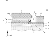
- FIG. 1 is a detailed plan view showing the configuration of the external electrode 4 of the thin film element 101 according to the first embodiment.
- 2 is a cross-sectional view taken along the line AA in FIG.
- FIG. 3 is a cross-sectional view showing an actual state of the external electrode 4 of the thin film element 101.
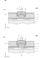
- 4A is a detailed cross-sectional view showing the configuration of the external electrode 4 of the thin film element 100A that does not include the protective film and the first resist film as a comparative example, and FIG. 4B shows the first resist film.
- FIG. 6 is a detailed cross-sectional view showing a configuration of an external electrode 4 of a thin film element 100B not including FIG. 5 is a cross-sectional view sequentially illustrating the manufacturing process of the thin film element 101.
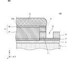
- FIG. 6 is a detailed cross-sectional view showing the configuration of the external electrode 4 of the thin film element 102 according to the second embodiment.
- FIG. 1 is a detailed plan view showing the configuration of the external electrode 4 of the thin film element 101 according to the first embodiment.
- 2 is a cross-sectional view taken along the line AA in FIG.
- FIG. 3 is a cross-sectional view showing an actual state of the external electrode 4 of the thin film element 101.
- the thin film element 101 is a thin film device (Thin-Film Device) such as a passive element such as a capacitor, an LC composite electronic component, a semiconductor integrated circuit element, or an ESD protection element.
- Thin-Film Device such as a passive element such as a capacitor, an LC composite electronic component, a semiconductor integrated circuit element, or an ESD protection element.
- the thin film element 101 includes a substrate 1, a wiring conductor film 2, a protective film 3, an external electrode 4, a conductive bonding material 5, a first resist film 11, and a second resist film 12.
- the substrate 1 is an insulating flat plate having a flat surface.
- a wiring conductor film 2 is formed on the surface of the substrate 1.
- the base material 1 is a base material for configuring, for example, passive elements, LC composite electronic components, integrated circuit elements, ESD protection elements, and the like, for example, a Si substrate or a glass substrate. Note that another insulating layer or wiring conductor layer may be provided between the substrate 1 and the wiring conductor film 2.
- the surface of the wiring conductor film 2 is covered with a protective film 3.
- the protective film 3 has a contact hole CH1 at a position overlapping the wiring conductor film 2 when viewed from the Z direction (in plan view). That is, the contact hole CH1 is formed in the protective film 3 at a position where the wiring conductor film 2 is formed as viewed from the Z direction.
- the contact hole CH1 is an opening formed in the protective film 3, and the wiring conductor film 2 is exposed from the contact hole CH1 by covering the surface of the wiring conductor film 2 with the protective film 3.
- the wiring conductor film 2 is a Cu film, for example.
- the protective film 3 is a metal film containing, for example, Ti as a main component.
- the external electrode 4 is a metal plating film having a circular planar shape, and has a first electrode layer 41 and a second electrode layer 42.
- the first electrode layer 41 is formed on the surface of the wiring conductor film 2, and the second electrode layer 42 is formed on the surface of the first electrode layer 41.
- the external electrode 4 is, for example, a metal plating film containing Ni as a main component.
- the first electrode layer 41 is, for example, a Ni plating film
- the second electrode layer 42 is, for example, an Au plating film.
- the external electrode 4 is formed on the surface of the wiring conductor film 2 exposed from the contact hole CH1. That is, the external electrode 4 is formed in the contact hole CH 1 and on the surface of the wiring conductor film 2. As shown in FIG. 1, the external electrode 4 is thicker than the protective film 3 and has a side surface S1. As shown in FIG. 1, the external electrode 4 has a side surface S1 formed in a reverse taper shape from the bottom surface to the surface. Therefore, the external electrode 4 has a flange portion 6 on the side surface S1. The flange 6 is formed along the entire circumference of the side surface S ⁇ b> 1 of the external electrode 4.
- the “protrusion” refers to the entire portion protruding from the bottom surface (base) of the external electrode 4 when viewed from the Z direction (in plan view).
- a conductive bonding material 5 is formed on the surface of the external electrode 4.
- the conductive bonding material 5 is, for example, solder precoated on the surface of the external electrode 4.
- the conductive bonding material 5 may be a solder ball temporarily fixed to the surface of the external electrode 4 with a flux or the like.
- the first resist film 11 is a thermosetting resin coated on the surface of the protective film 3, and is in contact with the entire circumference of the side surface S 1 of the external electrode 4. Therefore, the first resist film 11 according to the present embodiment has a loop shape (annular or ring shape that covers the interface between the external electrode 4 and the protective film 3, but may have a partially cut shape. ).
- the first resist film 11 is entirely accommodated in the flange portion 6 of the external electrode 4 as viewed from the Z direction. Therefore, the first resist film 11 is covered with the external electrode 4 (overlaid on the external electrode 4) as viewed from the Z direction.
- the first resist film 11 is, for example, a positive photosensitive solder resist film.
- the second resist film 12 is a thermosetting resin coated on the surface of the protective film 3, is made of the same resin as the first resist film 11, and is separated from the side surface S 1 of the external electrode 4 and the first resist film 11. Be placed. Accordingly, a separation portion 31 (clearance) is formed between the side surface S1 of the external electrode 4 and between the first resist film 11 and the second resist film 12, as shown in FIG.
- the second resist film 12 is, for example, a positive photosensitive solder resist film.
- the first resist film 11 and the second resist film are obtained by patterning the same resist film, but the height dimension of the first resist film 11 is smaller than the height dimension of the second resist film.
- FIG. 4A is a detailed cross-sectional view showing the configuration of the external electrode 4 of the thin film element 100A that does not include the protective film and the first resist film as a comparative example
- FIG. 4B shows the first resist film
- FIG. 6 is a detailed cross-sectional view showing a configuration of an external electrode 4 of a thin film element 100B not including
- a separation portion 31 is formed between the external electrode 4 and the second resist layer.
- the conductive bonding material 5 may infiltrate along the external electrode 4 from the spacing portion 31, and the wiring conductor film 2 exposed in the spacing portion 31 and the conductive bonding material 5 come into contact and react (solder).
- the resistance value increases and the wiring conductor film 2 is disconnected.
- moisture, flux, or the like may enter from the separation portion 31 and the wiring conductor film 2 exposed in the separation portion 31 may be corroded.
- the separation portion 31 is provided. Since the wiring conductor film 2 is not exposed inside, the reaction between the wiring conductor film 2 and the conductive bonding material 5 is suppressed. However, the interface 50 between the side surface of the external electrode 4 and the protective film 3 is only physically adjacent and in contact, and is not chemically bonded. Therefore, there is a possibility that the conductive bonding material 5, moisture, flux, or the like enters from the interface 50, and the wiring conductor film 2 and the conductive bonding material 5 react or the wiring conductor film 2 is corroded.
- the protective film 3 is coated on the surface of the wiring conductor film 2.
- the first resist film 11 is a loop-shaped thermosetting resin that covers the surface of the protective film 3, and is in contact with the entire circumference of the side surface S ⁇ b> 1 of the external electrode 4.
- the thin film element 101 includes the first resist film 11 that is in contact with the entire circumference of the side surface S1 of the external electrode 4, a conductive bonding material or moisture from the interface 50 between the side surface of the external electrode 4 and the protective film 3 is used. Intrusion of flux and the like is suppressed.
- first resist film 11 shrinks when cured, stress is generated in the cured loop-shaped first resist film 11 so as to be tightened inward (see the hollow arrow in FIG. 1). . Therefore, since the first resist film 11 coated on the surface of the protective film 3 fastens the side surface S1 of the external electrode 4, a conductive bonding material or moisture from the interface 50 between the side surface of the external electrode 4 and the protective film 3, Intrusion of flux or the like is further suppressed.
- the second resist film 12 is disposed away from the first resist film 11, and a separation portion 31 is formed between the first resist film 11 and the second resist layer. If the separation portion 31 is not provided, a stress is generated in the resist film from the interface with the external electrode 4 to the outside. Therefore, a gap is generated between the side surface of the external electrode 4 and the resist film. There is a risk that a conductive bonding material, moisture, flux or the like may enter.
- the cured second resist film 12 is subjected to stress outward from the external electrode 4 (see the arrow in FIG. 1), but the second resist film 12 is the same as the first resist film 11. Since they are spaced apart, the generation of a gap between the external electrode 4 and the resist film is further suppressed.
- the external electrode 4 of the present embodiment has a collar portion 6 formed along the entire circumference of the side surface S1, and the first resist film 11 overlaps the collar portion 6 as viewed from the Z direction. With this configuration, the hardened loop-shaped first resist film 11 can be prevented from dropping from the bottom surface of the external electrode 4 toward the surface.
- the thin film element 101 is manufactured by the following process, for example.
- FIG. 5 is a cross-sectional view sequentially illustrating the manufacturing process of the thin film element 101.
- a base material 1 in an aggregate substrate state is prepared, and a wiring conductor film 2 of about 1 ⁇ m is formed on the surface of the base material 1 by ion sputtering or the like.
- the substrate 1 is, for example, a Si substrate such as a passive element, an LC composite electronic component, an integrated circuit element, or an ESD protection element, and the wiring conductor film 2 is a metal film such as Cu. This step of forming the wiring conductor film 2 on the surface of the substrate 1 corresponds to the “first step” in the present invention.
- a protective film 3 of about 0.1 ⁇ m is continuously formed on the surface of the wiring conductor film 2 by ion sputtering or the like.
- the protective film 3 is a metal film whose main component is, for example, Ti.
- a positive photosensitive resist film having a thickness of about 5 ⁇ m is formed on the entire surface of the protective film 3 by spin coating, and is exposed and patterned.
- a tapered resist film 51 is formed from the bottom surface toward the surface.
- etching is performed using the resist film 51 as a mask to form a contact hole CH1 at a position overlapping the wiring conductor film 2 of the protective film 3.
- the wiring conductor film 2 is exposed from the contact hole CH1.
- This step of forming the protective film 3 on the surface of the wiring conductor film 2 and forming the contact hole CH1 at a position overlapping the wiring conductor film 2 of the protective film 3 corresponds to the “second step” in the present invention.
- the external electrode 4 is formed on the surface of the wiring conductor film 2 exposed in the contact hole CH1.
- a first electrode layer 41 having a thickness of about 3 ⁇ m and a second electrode layer 42 having a thickness of about 0.1 ⁇ m are continuously formed in the contact hole CH1 and on the surface of the wiring conductor film 2 by electrolytic plating.
- the first electrode layer 41 is a metal plating film containing Ni as a main component
- the second electrode layer 42 is a metal plating film containing Au as a main component.
- the metal plating film of the external electrode 4 grows along the tapered resist film 51 from the bottom surface to the surface. Therefore, the side surface of the external electrode 4 is formed in a reverse taper shape from the bottom surface to the surface, and the flange portion 6 is formed along the entire circumference of the side surface.
- This step of forming the external electrode 4 having the flange 6 along the entire circumference of the side surface in the contact hole CH1 and on the surface of the wiring conductor film 2 corresponds to the “third step” in the present invention.
- a resist film 10 of about 5 ⁇ m is formed on the surface of the protective film 3 and the external electrode 4 by spin coating.
- the resist film 10 is, for example, a positive photosensitive solder resist film. Note that the resist film 51 may be removed by a wet process using a peeling apparatus. This step of forming the resist film 10 on the surface of the protective film 3 corresponds to the “fourth step” in the present invention.
- a portion (first resist film 11) that overlaps the collar portion 6 in plan view, and other portions (second resist film) 12) is removed by photolithography.
- a portion of the resist film 10 that is not to be removed is covered with a photomask 61 and exposed to light L1.
- the flange 6 of the external electrode 4 serves as a photomask, and the portion overlapping the flange 6 in a plan view is not exposed. Therefore, after developing and washing (rinsing), the first resist film 11 and the second resist film 12 are exposed.
- the separation portion 31 that separates the two is removed.
- the light beam L1 is, for example, ultraviolet light (UV light).
- the fifth step includes a step of exposing the flange portion 6 of the external electrode 4 using a photomask.
- the conductive bonding material 5 is, for example, solder.
- the conductive bonding material 5 may be formed by a reflow process after screen printing of a solder paste. Alternatively, a flux or the like may be applied to the surface of the external electrode 4, and solder balls may be mounted and temporarily fixed, and then formed by a reflow process. Furthermore, the conductive bonding material 5 may be in a state in which a solder ball is temporarily fixed by applying a flux or the like to the surface of the external electrode 4.
- the resist film 10 is a positive photosensitive resist film, and the flange portion 6 of the external electrode 4 serves as a photomask. Therefore, the first resist film that is in contact with the entire circumference of the side surface of the external electrode 4. 11 can be formed easily.
- Second Embodiment An example in which the shapes of the external electrode 4 and the first resist film 11 are different from those of the first embodiment is shown.
- FIG. 6 is a detailed cross-sectional view showing the configuration of the external electrode 4 of the thin film element 102 according to the second embodiment.
- the external electrode 4 As shown in FIG. 6, the external electrode 4 according to this embodiment has a shape in which the upper part of the side surface protrudes like a screw head. Even in such a structure, the external electrode 4 has the flange portion 6 formed along the entire circumference of the side surface. Further, the first resist film 11 is in contact with the entire circumference of the side surface of the external electrode 4, and the whole is accommodated in the flange portion 6 of the external electrode 4 as viewed from the Z direction.
- planar shape of the external electrode 4 is circular has been shown, but the present invention is not limited thereto.
- the planar shape of the external electrode 4 can be appropriately changed to a square, a rectangle, a polygon, an ellipse, or the like.
- the flange 6 is not limited to the one formed on the upper part of the side surface of the external electrode 4.
- the flange portion 6 may be a portion that protrudes from the bottom surface (base portion) of the external electrode 4 when viewed from the Z direction, and may be formed on a portion other than the bottom surface of the external electrode 4. That is, the flange 6 may be formed at the center of the side surface of the external electrode 4 or the like.
- the wiring conductor film 2 is not limited to the one formed on the entire surface of the substrate 1, and may be formed only on a part of the surface of the substrate 1.
- the protective film 3 should just be formed in the surface of the wiring conductor film 2 at least, and may be formed in the surface of the base material 1.
- the surface of the substrate 1 may be a curved surface, or there may be a step on the surface of the substrate 1.
Landscapes
- Engineering & Computer Science (AREA)
- Power Engineering (AREA)
- Microelectronics & Electronic Packaging (AREA)
- Manufacturing & Machinery (AREA)
- Chemical & Material Sciences (AREA)
- Materials Engineering (AREA)
- Non-Metallic Protective Coatings For Printed Circuits (AREA)
- Internal Circuitry In Semiconductor Integrated Circuit Devices (AREA)
Abstract
薄膜素子(101)は、基材(1)、基材(1)の表面に形成される配線導体膜(2)、少なくとも配線導体膜(2)の表面に被覆される保護膜(3)、外部電極(4)、保護膜(3)の表面に被覆される第1レジスト膜(11)および第2レジスト膜(12)を備える。保護膜(3)は(Z)方向から視て配線導体膜(2)と重なる位置にコンタクトホール(CH1)を有し、外部電極(4)はコンタクトホール(CH1)内、且つ、配線導体膜(2)の表面に形成される。外部電極(4)は保護膜(3)より厚く、側面(S1)を有する。第1レジスト膜(11)は、外部電極(4)の側面(S1)の全周に沿って接し、第2レジスト膜(12)は、外部電極(4)の側面(S1)および第1レジスト膜(11)から離間して配置される。
Description
本発明は、薄膜素子に関し、特に例えば、基材と基材上に形成される配線導体膜と、配線導体膜上に形成される外部電極とを有する薄膜素子に関する。また、その薄膜素子の製造方法に関する。
従来、基材と、基材上に形成される配線導体膜と、配線導体膜の表面に形成される外部電極と、基材の表面および配線導体膜の表面に被覆されるレジスト膜と、外部電極の表面に形成されるはんだバンプと、を備える端子構造が知られている(特許文献1)。
また、特許文献1に開示されているように、はんだ等の導電性接合材を外部電極に接合する際に、基材上に形成された配線導体膜や外部電極が、基材から剥離することを防止するため、配線導体膜や外部電極の外縁にレジスト膜を被せる方法(オーバーレジスト処理)が一般的である。
しかし、外部電極を構成するAuははんだに濡れやすく、はんだを外部電極に接合する際に、外部電極の表面とレジスト層との界面にはんだが浸入し、外部電極の表面がオーバーレジスト処理したレジスト層の剥離の起点となる虞がある。
一方、このようなレジスト層の剥離を抑制するため、レジスト層と外部電極との間に所定間隔(クリアランス)が設けられたクリアランスレジスト型の端子構造もある(特許文献2)。
しかし、レジスト層と外部電極との間に所定クリアランスを設けた場合、上記クリアランスからはんだが浸入し、上記クリアランス内で露出する配線導体膜とはんだとが反応すること(はんだ食われ等)によって、抵抗値の増大や、配線導体膜が断線する虞がある。また、上記クリアランスから水分やフラックス等が浸入し、上記クリアランス内に露出する配線導体膜が腐食する虞もある。
本発明の目的は、レジスト層を外部電極から離間して配置する構造において、配線導体膜のはんだ食われや腐食等を抑制した、信頼性の高い外部電極を有する薄膜素子を提供することにある。また、その薄膜素子の製造方法を提供することにある。
(1)本発明の薄膜素子は、
基材と、
前記基材の表面に形成される配線導体膜と、
少なくとも前記配線導体膜の表面に被覆され、平面視で前記配線導体膜と重なる位置にコンタクトホールを有する保護膜と、
前記コンタクトホール内、且つ、前記配線導体膜の表面に形成され、前記保護膜より厚く、側面を有する外部電極と、
前記保護膜の表面に被覆される第1レジスト膜および第2レジスト膜と、
を備え、
前記第1レジスト膜は、前記外部電極の前記側面の全周に沿って接し、
前記第2レジスト膜は、前記外部電極の前記側面および前記第1レジスト膜から離間して配置されることを特徴とする。
基材と、
前記基材の表面に形成される配線導体膜と、
少なくとも前記配線導体膜の表面に被覆され、平面視で前記配線導体膜と重なる位置にコンタクトホールを有する保護膜と、
前記コンタクトホール内、且つ、前記配線導体膜の表面に形成され、前記保護膜より厚く、側面を有する外部電極と、
前記保護膜の表面に被覆される第1レジスト膜および第2レジスト膜と、
を備え、
前記第1レジスト膜は、前記外部電極の前記側面の全周に沿って接し、
前記第2レジスト膜は、前記外部電極の前記側面および前記第1レジスト膜から離間して配置されることを特徴とする。
この構成では、外部電極の側面および第1レジスト膜と第2レジスト膜との間に形成された離間部内に配線導体膜が露出しないため、この離間部から導電性接合材や水分、フラックス等が浸入したとしても、配線導体膜と導電性接合材5の反応等は抑制される。
また、この構成では、外部電極の側面の全周に沿って接する第1レジスト膜を備えるため、外部電極の側面と保護膜との界面からの導電性接合材や水分、フラックス等の浸入が抑制される。
(2)上記(1)において、前記第1レジスト膜は熱硬化性樹脂であることが好ましい。この構成により、第1レジスト膜はキュアした際に収縮するため、硬化したループ状の第1レジスト膜には内側に向かって締まるような応力が発生する。したがって、保護膜の表面に被覆される第1レジスト膜が、外部電極の側面を締め付けるため、外部電極の側面と保護膜との界面からの導電性接合材や水分、フラックス等の浸入が抑制される。
また、この構成により、硬化した第2レジスト膜には外部電極から外側に向かう応力が発生するが、第2レジスト膜は第1レジスト膜と離間して配置されているため、外部電極と第1レジスト膜との間の隙間の発生がさらに抑制される。
(3)上記(1)または(2)において、前記外部電極は、前記側面の全周に沿って形成される庇部を有し、前記第1レジスト膜は、平面視で前記庇部に重なることが好ましい。この構成により、硬化したループ状の第1レジスト膜が、外部電極の底面から表面に向かって脱落することを抑制できる。
(4)上記(3)において、前記外部電極は、底面から表面に向かって前記側面が逆テーパー状に形成されていてもよい。
(5)上記(1)から(4)のいずれかにおいて、前記配線導体膜は銅を主成分とする金属膜であり、前記保護膜はチタンを主成分とする金属膜であり、前記外部電極はニッケルを主成分とする金属であってもよい。
(6)本発明の薄膜素子の製造方法は、
基材の表面に配線導体膜を形成する第1工程と、
少なくとも前記配線導体膜の表面に、前記配線導体膜と重なる位置にコンタクトホールを有する保護膜を被覆する第2工程と、
前記コンタクトホール内、且つ、前記配線導体膜の表面に、側面の全周に沿って庇部を有する外部電極を形成する第3工程と、
前記保護膜の表面にレジスト膜を被覆する第4工程と、
前記レジスト膜のうち、平面視で前記庇部に重なる第1レジスト膜と、前記第1レジスト膜以外である第2レジスト膜とを離間する離間部を除去する第5工程と、
を備えることを特徴とする。
基材の表面に配線導体膜を形成する第1工程と、
少なくとも前記配線導体膜の表面に、前記配線導体膜と重なる位置にコンタクトホールを有する保護膜を被覆する第2工程と、
前記コンタクトホール内、且つ、前記配線導体膜の表面に、側面の全周に沿って庇部を有する外部電極を形成する第3工程と、
前記保護膜の表面にレジスト膜を被覆する第4工程と、
前記レジスト膜のうち、平面視で前記庇部に重なる第1レジスト膜と、前記第1レジスト膜以外である第2レジスト膜とを離間する離間部を除去する第5工程と、
を備えることを特徴とする。
この製造方法により、配線導体膜のはんだ食われや腐食等を抑制した、信頼性の高い外部電極を有する薄膜素子を容易に製造できる。
(7)上記(6)において、前記第5工程は、前記レジスト膜はポジ型感光性レジスト膜であり、前記離間部をフォトリソグラフィにより除去し、前記外部電極の前記庇部をフォトマスクにして露光する工程を含むことが好ましい。この製造方法により、外部電極の側面の全周に沿って接する第1レジスト膜を容易に形成できる。
(8)上記(6)または(7)において、前記第5工程の後に、前記外部電極の表面にはんだをプリコートする工程をさらに有していてもよい。
本発明によれば、レジスト層と外部電極との間に所定のクリアランスを設ける構造において、配線導体膜のはんだ食われや腐食等を抑制した、信頼性の高い外部電極を有する薄膜素子を実現できる。
以降、図を参照して幾つかの具体的な例を挙げて、本発明を実施するための複数の形態を示す。各図中には同一箇所に同一符号を付している。要点の説明または理解の容易性を考慮して、便宜上実施形態を分けて示すが、異なる実施形態で示した構成の部分的な置換または組み合わせが可能である。第2の実施形態以降では第1の実施形態と共通の事柄についての記述を省略し、異なる点についてのみ説明する。特に、同様の構成による同様の作用効果については実施形態毎には逐次言及しない。
《第1の実施形態》
図1は第1の実施形態に係る薄膜素子101の外部電極4の構成を示す平面詳細図である。図2は、図1におけるA-A断面図である。図3は薄膜素子101の外部電極4の実際の様子を示す断面図である。図2において、各部の厚みは誇張して図示している。以降の各実施形態における断面図についても同様である。薄膜素子101は、例えばキャパシタ等の受動素子やLC複合電子部品、半導体集積回路素子、ESD保護素子等の薄膜デバイス(Thin-Film Device)である。
図1は第1の実施形態に係る薄膜素子101の外部電極4の構成を示す平面詳細図である。図2は、図1におけるA-A断面図である。図3は薄膜素子101の外部電極4の実際の様子を示す断面図である。図2において、各部の厚みは誇張して図示している。以降の各実施形態における断面図についても同様である。薄膜素子101は、例えばキャパシタ等の受動素子やLC複合電子部品、半導体集積回路素子、ESD保護素子等の薄膜デバイス(Thin-Film Device)である。
薄膜素子101は、基材1、配線導体膜2、保護膜3、外部電極4、導電性接合材5、第1レジスト膜11、第2レジスト膜12を備える。
基材1は表面が平面状の絶縁性平板である。基材1の表面には配線導体膜2が形成されている。基材1は例えば受動素子やLC複合電子部品、集積回路素子、ESD保護素子等を構成するためのベース材であり、例えばSi基板やガラス基板である。なお、基材1と配線導体膜2との間には、他の絶縁層や配線導体層が設けられていてもよい。
配線導体膜2の表面には保護膜3が被覆されている。保護膜3は、図2に示すように、Z方向から視て(平面視で)配線導体膜2と重なる位置にコンタクトホールCH1を有する。すなわち、保護膜3には、Z方向から視て、配線導体膜2が形成されている位置にコンタクトホールCH1が形成されている。コンタクトホールCH1は保護膜3に形成される開口であり、配線導体膜2の表面に保護膜3が被覆されることにより、コンタクトホールCH1から配線導体膜2が露出する。配線導体膜2は例えばCu膜である。保護膜3は例えばTiを主成分とする金属膜である。
外部電極4は平面形状が円形の金属めっき膜であり、第1電極層41および第2電極層42を有する。第1電極層41は配線導体膜2の表面に形成され、第2電極層42は第1電極層41の表面に形成されている。外部電極4は例えばNiを主成分とする金属めっき膜である。第1電極層41は例えばNiめっき膜であり、第2電極層42は例えばAuめっき膜である。
外部電極4は、コンタクトホールCH1から露出する配線導体膜2の表面に形成される。すなわち、外部電極4はコンタクトホールCH1内、且つ、配線導体膜2の表面に形成される。図1に示すように、外部電極4は保護膜3より厚く、側面S1を有する。図1に示すように、外部電極4は底面から表面に向かって側面S1が逆テーパー状に形成される。そのため、外部電極4は側面S1に庇部6を有する。庇部6は外部電極4の側面S1の全周に沿って形成される。なお、本発明における「庇部」とは、Z方向から視て(平面視で)、外部電極4の底面(基部)よりもはみ出した部分全体をいう。
外部電極4の表面には導電性接合材5が形成されている。導電性接合材5は、例えば外部電極4の表面にプリコートされたはんだである。なお、導電性接合材5は、フラックス等で外部電極4の表面に仮固定されたはんだボールであってもよい。
第1レジスト膜11は保護膜3の表面に被覆される熱硬化性樹脂であり、外部電極4の側面S1の全周に沿って接している。そのため、本実施形態に係る第1レジスト膜11は、外部電極4と保護膜3との界面を覆うようなループ状(環状、リング状。但し、部分的に切れた形状であってもよい。)である。第1レジスト膜11は、Z方向から視て、全体が外部電極4の庇部6内に収まる。したがって、第1レジスト膜11は、Z方向から視て、外部電極4で覆われている(外部電極4に重なっている)。第1レジスト膜11は例えばポジ型感光性のソルダーレジスト膜である。
第2レジスト膜12は保護膜3の表面に被覆される熱硬化性樹脂であり、第1レジスト膜11と同じ樹脂で構成され、外部電極4の側面S1および第1レジスト膜11から離間して配置される。したがって、外部電極4の側面S1および第1レジスト膜11と第2レジスト膜12との間には、図2等に示すように、離間部31(クリアランス)が形成されている。第2レジスト膜12は例えばポジ型感光性のソルダーレジスト膜である。第1レジスト膜11および第2レジスト膜は同一のレジスト膜をパターニングしたものであるが、第1レジスト膜11の高さ寸法は第2レジスト膜の高さ寸法よりも小さい。
次に、保護膜3および第1レジスト膜11を備えることの利点について、図を参照して説明する。図4(A)は、比較例として、保護膜および第1レジスト膜を備えていない薄膜素子100Aの外部電極4の構成を示す断面詳細図であり、図4(B)は、第1レジスト膜を備えていない薄膜素子100Bの外部電極4の構成を示す断面詳細図である。
図4(A)に示すように、外部電極4と第2レジスト層との間には離間部31が形成されている。そのため、この離間部31から外部電極4に沿って導電性接合材5が浸入することがあり、離間部31内に露出する配線導体膜2と導電性接合材5とが接触して反応(はんだ食われ等)し、抵抗値の増大や、配線導体膜2が断線する虞がある。また、上記離間部31から水分やフラックス等が浸入し、上記離間部31内に露出する配線導体膜2が腐食する虞もある。
また、図4(B)に示すように、配線導体膜2の表面に保護膜3が被覆されている場合には、この離間部31から導電性接合材5が浸入しても、離間部31内に配線導体膜2が露出していないため、配線導体膜2と導電性接合材5との反応は抑制される。しかし、外部電極4の側面と保護膜3との界面50は物理的に隣接・接触しているだけであり、化学的に結合してはいない。そのため、導電性接合材5や水分、フラックス等がこの界面50から浸入し、配線導体膜2と導電性接合材5とが反応したり、配線導体膜2が腐食する虞がある。
一方、本実施形態では、保護膜3が配線導体膜2の表面に被覆される。また、本実施形態では、第1レジスト膜11が、保護膜3の表面に被覆されるループ状の熱硬化性樹脂であり、外部電極4の側面S1の全周に沿って接している。この構成では、離間部31内で配線導体膜2が露出しないため、この離間部31から導電性接合材5や水分、フラックス等が浸入したとしても、配線導体膜2と導電性接合材5との反応等は抑制される。また、薄膜素子101は、外部電極4の側面S1の全周に沿って接する第1レジスト膜11を備えるため、外部電極4の側面と保護膜3との界面50からの導電性接合材や水分、フラックス等の浸入が抑制される。
さらに、第1レジスト膜11はキュアした際に収縮するため、硬化したループ状の第1レジスト膜11には内側に向かって締まるような応力が発生する(図1中の中抜き矢印を参照)。したがって、保護膜3の表面に被覆される第1レジスト膜11が、外部電極4の側面S1を締め付けるため、外部電極4の側面と保護膜3との界面50からの導電性接合材や水分、フラックス等の浸入がさらに抑制される。
また、本実施形態では、第2レジスト膜12が第1レジスト膜11と離間して配置され、第1レジスト膜11と第2レジスト層との間に離間部31が形成されている。もし離間部31が設けられていない場合、レジスト膜には外部電極4との界面から外側に向かう応力が発生するため、外部電極4の側面とレジスト膜との間に隙間が生じ、この隙間から導電性接合材や水分、フラックス等が浸入する虞がある。一方、本実施形態では、硬化した第2レジスト膜12には外部電極4から外側に向かう応力が発生するが(図1中の矢印を参照)、第2レジスト膜12は第1レジスト膜11と離間して配置されているため、外部電極4とレジスト膜との間の隙間の発生がさらに抑制される。
また、本実施形態の外部電極4は、側面S1の全周に沿って形成される庇部6を有し、第1レジスト膜11が、Z方向から視て庇部6に重なっている。この構成により、硬化したループ状の第1レジスト膜11が、外部電極4の底面から表面に向かって脱落することを抑制できる。
上記薄膜素子101は例えば次の工程で製造される。図5は、薄膜素子101の製造工程を順に示す断面図である。
まず、図5中の(1)に示すように、集合基板状態の基材1を用意し、基材1の表面に、イオンスパッタリング等によって約1μmの配線導体膜2を形成する。基材1は例えば受動素子やLC複合電子部品、集積回路素子、ESD保護素子等のSi基板等であり、配線導体膜2は例えばCu等の金属膜である。基材1の表面に配線導体膜2を形成するこの工程が、本発明における「第1工程」に相当する。
次に、配線導体膜2の表面に、イオンスパッタリング等によって約0.1μmの保護膜3を連続形成する。保護膜3は例えばTi等を主成分とする金属膜である。その後、スピンコートによって保護膜3の全面に約5μmのポジ型感光性のレジスト膜を形成し、露光してパターニングする。この工程により、底面から表面に向かってテーパー状のレジスト膜51が形成される。さらに、レジスト膜51をマスクとしてエッチングを行い、保護膜3の配線導体膜2と重なる位置にコンタクトホールCH1を形成する。この工程により、コンタクトホールCH1から配線導体膜2が露出する。配線導体膜2の表面に保護膜3を形成し、保護膜3の配線導体膜2と重なる位置にコンタクトホールCH1を形成するこの工程が、本発明における「第2工程」に相当する。
次に図5中の(2)に示すように、コンタクトホールCH1に露出する配線導体膜2の表面に、外部電極4を形成する。具体的には、コンタクトホールCH1内、且つ、配線導体膜2の表面に、電解めっき法によって、約3μmの第1電極層41および約0.1μmの第2電極層42を連続形成する。第1電極層41は例えばNiを主成分とする金属めっき膜であり、第2電極層42はAuを主成分とする金属めっき膜である。
外部電極4の金属めっき膜は、底面から表面に向かってテーパー状のレジスト膜51に沿って成長する。そのため、外部電極4は、底面から表面に向かって側面が逆テーパー状に形成され、その側面の全周に沿って庇部6が形成される。コンタクトホールCH1内、且つ、配線導体膜2の表面に、側面の全周に沿って庇部6を有する外部電極4を形成するこの工程が、本発明における「第3工程」に相当する。
次に図5中の(4)に示すように、レジスト膜51をアッシングにより取り除いた後、スピンコートによって保護膜3および外部電極4の表面に約5μmのレジスト膜10を形成する。レジスト膜10は例えばポジ型感光性のソルダーレジスト膜である。なお、レジスト膜51はウェット処理で剥離装置にかけて取り除いてもよい。保護膜3の表面にレジスト膜10を形成するこの工程が、本発明における「第4工程」に相当する。
次に図5中の(5)(6)に示すように、レジスト膜10のうち、平面視で庇部6に重なる部分(第1レジスト膜11)と、それ以外の部分(第2レジスト膜12)とを離間する離間部31をフォトリソグラフィにより除去する。具体的には、レジスト膜10のうち、除去したくない部分にフォトマスク61を被せて、光線L1で露光する。このとき、外部電極4の庇部6がフォトマスクとなり、平面視で庇部6に重なる部分は露光されないため、現像して洗浄(リンス)した後、第1レジスト膜11と第2レジスト膜12とを離間する離間部31が除去される。光線L1は例えば紫外線(UV光)である。
レジスト膜10のうち、平面視で庇部6に重なる第1レジスト膜11と、第2レジスト膜12とを離間する離間部31を除去するこの工程が、本発明における「第5工程」に相当する。そして、この第5工程は外部電極4の庇部6をフォトマスクにして露光する工程を含む。
上記第5工程の後に、外部電極4の表面に導電性接合材5をプリコートする。導電性接合材5は例えばはんだである。なお、導電性接合材5ははんだペーストをスクリーン印刷した後、リフロープロセスによって形成してもよい。また、外部電極4の表面にフラックス等を塗付して、はんだボールをマウントして仮固定した後、リフロープロセスによって形成してもよい。さらに、導電性接合材5は、外部電極4の表面にフラックス等を塗付して、はんだボールを仮固定した状態であってもよい。
上記製造方法により、配線導体膜2のはんだ食われや腐食等を抑制した、信頼性の高い外部電極4を有する薄膜素子101を容易に製造できる。
また、上記製造方法では、レジスト膜10がポジ型感光性レジスト膜であり、外部電極4の庇部6がフォトマスクとなるため、外部電極4の側面の全周に沿って接する第1レジスト膜11を容易に形成できる。
《第2の実施形態》
第2の実施形態では、外部電極4および第1レジスト膜11の形状が第1の実施形態とは異なる例を示す。
第2の実施形態では、外部電極4および第1レジスト膜11の形状が第1の実施形態とは異なる例を示す。
図6は、第2の実施形態に係る薄膜素子102の外部電極4の構成を示す断面詳細図である。
本実施形態に係る外部電極4は、図6に示すように、ネジ頭のように側面上部が突出した形状である。このような構造であっても、外部電極4は側面の全周に沿って形成される庇部6を有する。また、第1レジスト膜11は外部電極4の側面の全周に沿って接しており、Z方向から視て、全体が外部電極4の庇部6内に収まる。
《その他の実施形態》
なお、上述の実施形態では、外部電極4の平面形状が円形である例を示したが、これ限定されるものではない。外部電極4の平面形状は、正方形、矩形、多角形、楕円形等、適宜変更可能である。
なお、上述の実施形態では、外部電極4の平面形状が円形である例を示したが、これ限定されるものではない。外部電極4の平面形状は、正方形、矩形、多角形、楕円形等、適宜変更可能である。
また、庇部6は、外部電極4の側面上部に形成されるものに限定されるものではない。庇部6は、Z方向から視て、外部電極4の底面(基部)からはみ出した部分であればよく、外部電極4の底面以外に形成されていればよい。すなわち、庇部6は、外部電極4の側面中央部等に形成されていてもよい。
また、配線導体膜2は基材1の表面全体に形成されるものに限定されるものではなく、基材1の表面の一部にのみ形成されていてもよい。また、保護膜3は少なくとも配線導体膜2の表面に形成されていればよく、基材1の表面に形成されていてもよい。
なお、上述の実施形態では、基材1の表面が平面状である例を示したが、これに限定されるものではない。基材1の表面は、曲面であってもよく、基材1の表面に段差があってもよい。
CH1…コンタクトホール
L1…光線
S1…外部電極の側面
1…基材
2…配線導体膜
3…保護膜
4…外部電極
5…導電性接合材
6…庇部
10…レジスト膜
11…第1レジスト膜
12…第2レジスト膜
31…離間部
41…第1電極層
42…第2電極層
50…界面
51…レジスト膜
61…フォトマスク
100A,100B,101,102…薄膜素子
L1…光線
S1…外部電極の側面
1…基材
2…配線導体膜
3…保護膜
4…外部電極
5…導電性接合材
6…庇部
10…レジスト膜
11…第1レジスト膜
12…第2レジスト膜
31…離間部
41…第1電極層
42…第2電極層
50…界面
51…レジスト膜
61…フォトマスク
100A,100B,101,102…薄膜素子
Claims (8)
- 基材と、
前記基材の表面に形成される配線導体膜と、
少なくとも前記配線導体膜の表面に被覆され、平面視で前記配線導体膜と重なる位置にコンタクトホールを有する保護膜と、
前記コンタクトホール内、且つ、前記配線導体膜の表面に形成され、前記保護膜より厚く、側面を有する外部電極と、
前記保護膜の表面に被覆される第1レジスト膜および第2レジスト膜と、
を備え、
前記第1レジスト膜は、前記外部電極の前記側面の全周に沿って接し、
前記第2レジスト膜は、前記外部電極の前記側面および前記第1レジスト膜から離間して配置される、薄膜素子。 - 前記第1レジスト膜は熱硬化性樹脂である、請求項1に記載の薄膜素子。
- 前記外部電極は、前記側面の全周に沿って形成される庇部を有し、
前記第1レジスト膜は、平面視で前記庇部に重なる、請求項1または2に記載の薄膜素子。 - 前記外部電極は、底面から表面に向かって前記側面が逆テーパー状に形成される、請求項3に記載の薄膜素子。
- 前記配線導体膜は銅を主成分とする金属膜であり、
前記保護膜はチタンを主成分とする金属膜であり、
前記外部電極はニッケルを主成分とする金属である、請求項1から4のいずれかに記載の薄膜素子。 - 基材の表面に配線導体膜を形成する第1工程と、
少なくとも前記配線導体膜の表面に、前記配線導体膜と重なる位置にコンタクトホールを有する保護膜を被覆する第2工程と、
前記コンタクトホール内、且つ、前記配線導体膜の表面に、側面の全周に沿って庇部を有する外部電極を形成する第3工程と、
前記保護膜の表面にレジスト膜を被覆する第4工程と、
前記レジスト膜のうち、平面視で前記庇部に重なる第1レジスト膜と、前記第1レジスト膜以外である第2レジスト膜とを離間する離間部を除去する第5工程と、
を備える、薄膜素子の製造方法。 - 前記第5工程は、
前記レジスト膜はポジ型感光性レジスト膜であり、前記離間部をフォトリソグラフィにより除去し、
前記外部電極の前記庇部をフォトマスクにして露光する工程を含む、請求項6に記載の薄膜素子の製造方法。 - 前記第5工程の後に、前記外部電極の表面にはんだをプリコートする工程をさらに有する、請求項6または7に記載の薄膜素子の製造方法。
Priority Applications (3)
| Application Number | Priority Date | Filing Date | Title |
|---|---|---|---|
| JP2017547728A JP6341336B2 (ja) | 2015-10-30 | 2016-10-14 | 薄膜素子およびその製造方法 |
| CN201690001309.5U CN208706584U (zh) | 2015-10-30 | 2016-10-14 | 薄膜元件 |
| US15/941,237 US10388603B2 (en) | 2015-10-30 | 2018-03-30 | Thin film element and method for manufacturing the same |
Applications Claiming Priority (2)
| Application Number | Priority Date | Filing Date | Title |
|---|---|---|---|
| JP2015-214182 | 2015-10-30 | ||
| JP2015214182 | 2015-10-30 |
Related Child Applications (1)
| Application Number | Title | Priority Date | Filing Date |
|---|---|---|---|
| US15/941,237 Continuation US10388603B2 (en) | 2015-10-30 | 2018-03-30 | Thin film element and method for manufacturing the same |
Publications (1)
| Publication Number | Publication Date |
|---|---|
| WO2017073350A1 true WO2017073350A1 (ja) | 2017-05-04 |
Family
ID=58630067
Family Applications (1)
| Application Number | Title | Priority Date | Filing Date |
|---|---|---|---|
| PCT/JP2016/080467 Ceased WO2017073350A1 (ja) | 2015-10-30 | 2016-10-14 | 薄膜素子およびその製造方法 |
Country Status (4)
| Country | Link |
|---|---|
| US (1) | US10388603B2 (ja) |
| JP (1) | JP6341336B2 (ja) |
| CN (1) | CN208706584U (ja) |
| WO (1) | WO2017073350A1 (ja) |
Citations (2)
| Publication number | Priority date | Publication date | Assignee | Title |
|---|---|---|---|---|
| JP2003124389A (ja) * | 2001-10-10 | 2003-04-25 | Fujikura Ltd | 半導体パッケージ |
| JP2010267641A (ja) * | 2009-05-12 | 2010-11-25 | Panasonic Corp | 半導体装置 |
Family Cites Families (9)
| Publication number | Priority date | Publication date | Assignee | Title |
|---|---|---|---|---|
| US6426556B1 (en) * | 2001-01-16 | 2002-07-30 | Megic Corporation | Reliable metal bumps on top of I/O pads with test probe marks |
| CN100590859C (zh) * | 2007-01-16 | 2010-02-17 | 百慕达南茂科技股份有限公司 | 具有环状支撑物的凸块结构及其制造方法 |
| JP2009231682A (ja) | 2008-03-25 | 2009-10-08 | Citizen Watch Co Ltd | 半導体装置およびその製造方法 |
| JP2009266803A (ja) | 2008-04-03 | 2009-11-12 | Fuji Electric Holdings Co Ltd | 有機elディスプレイパネル及びその製造方法 |
| US8598030B2 (en) * | 2010-08-12 | 2013-12-03 | Taiwan Semiconductor Manufacturing Company, Ltd. | Process for making conductive post with footing profile |
| JP2012074487A (ja) | 2010-09-28 | 2012-04-12 | Toppan Printing Co Ltd | 半導体パッケージの製造方法 |
| JP5862210B2 (ja) | 2011-11-07 | 2016-02-16 | 株式会社村田製作所 | 高周波電子部品 |
| JP6238007B2 (ja) | 2013-03-02 | 2017-11-29 | 荒川化学工業株式会社 | クリアランスレジスト用鉛フリーはんだ向けフラックスおよびクリアランスレジスト用鉛フリーはんだペースト |
| US9779969B2 (en) * | 2014-03-13 | 2017-10-03 | Taiwan Semiconductor Manufacturing Co., Ltd. | Package structure and manufacturing method |
-
2016
- 2016-10-14 JP JP2017547728A patent/JP6341336B2/ja active Active
- 2016-10-14 CN CN201690001309.5U patent/CN208706584U/zh active Active
- 2016-10-14 WO PCT/JP2016/080467 patent/WO2017073350A1/ja not_active Ceased
-
2018
- 2018-03-30 US US15/941,237 patent/US10388603B2/en active Active
Patent Citations (2)
| Publication number | Priority date | Publication date | Assignee | Title |
|---|---|---|---|---|
| JP2003124389A (ja) * | 2001-10-10 | 2003-04-25 | Fujikura Ltd | 半導体パッケージ |
| JP2010267641A (ja) * | 2009-05-12 | 2010-11-25 | Panasonic Corp | 半導体装置 |
Also Published As
| Publication number | Publication date |
|---|---|
| US10388603B2 (en) | 2019-08-20 |
| US20180226346A1 (en) | 2018-08-09 |
| CN208706584U (zh) | 2019-04-05 |
| JP6341336B2 (ja) | 2018-06-13 |
| JPWO2017073350A1 (ja) | 2018-04-12 |
Similar Documents
| Publication | Publication Date | Title |
|---|---|---|
| JP4922891B2 (ja) | 半導体装置およびその製造方法 | |
| CN101548378B (zh) | 半导体器件及其制造方法 | |
| TWI473552B (zh) | 具有元件設置區之基板結構及其製程 | |
| US7781338B2 (en) | Semiconductor device manufacturing method and semiconductor device | |
| JP4450071B2 (ja) | 電子部品 | |
| JP5385452B2 (ja) | 半導体装置の製造方法 | |
| JP7134617B2 (ja) | 半導体装置及び半導体装置の製造方法 | |
| JP4506767B2 (ja) | 半導体装置の製造方法 | |
| JP6341336B2 (ja) | 薄膜素子およびその製造方法 | |
| CN103426775B (zh) | 半导体装置的制造方法 | |
| CN106252315B (zh) | 封装结构及其制造方法 | |
| JP6328741B2 (ja) | 半導体装置 | |
| JP3972211B2 (ja) | 半導体装置及びその製造方法 | |
| US9922923B2 (en) | Method of manufacturing wiring substrate and wiring substrate | |
| JP2010062170A (ja) | 半導体装置およびその製造方法 | |
| TWI577248B (zh) | 線路載板及其製作方法 | |
| JP4873179B2 (ja) | 半導体装置の製造方法 | |
| US7615474B2 (en) | Method for manufacturing semiconductor device with reduced damage to metal wiring layer | |
| JP7335036B2 (ja) | 半導体パッケージの製造方法 | |
| CN119965179A (zh) | 布线基板及其制造方法 | |
| JP5068830B2 (ja) | 半導体装置 | |
| JP2008258439A (ja) | 半導体装置の製造方法 | |
| JP2011171660A (ja) | 電子部品の製造方法 | |
| JP2010157545A (ja) | 半導体装置の製造方法 |
Legal Events
| Date | Code | Title | Description |
|---|---|---|---|
| 121 | Ep: the epo has been informed by wipo that ep was designated in this application |
Ref document number: 16859585 Country of ref document: EP Kind code of ref document: A1 |
|
| ENP | Entry into the national phase |
Ref document number: 2017547728 Country of ref document: JP Kind code of ref document: A |
|
| NENP | Non-entry into the national phase |
Ref country code: DE |
|
| 122 | Ep: pct application non-entry in european phase |
Ref document number: 16859585 Country of ref document: EP Kind code of ref document: A1 |