WO2017061334A1 - 気相成長装置および異常検出方法 - Google Patents
気相成長装置および異常検出方法 Download PDFInfo
- Publication number
- WO2017061334A1 WO2017061334A1 PCT/JP2016/079070 JP2016079070W WO2017061334A1 WO 2017061334 A1 WO2017061334 A1 WO 2017061334A1 JP 2016079070 W JP2016079070 W JP 2016079070W WO 2017061334 A1 WO2017061334 A1 WO 2017061334A1
- Authority
- WO
- WIPO (PCT)
- Prior art keywords
- value
- threshold
- unit
- heating
- detection method
- Prior art date
- Legal status (The legal status is an assumption and is not a legal conclusion. Google has not performed a legal analysis and makes no representation as to the accuracy of the status listed.)
- Ceased
Links
Images

Classifications
-
- C—CHEMISTRY; METALLURGY
- C23—COATING METALLIC MATERIAL; COATING MATERIAL WITH METALLIC MATERIAL; CHEMICAL SURFACE TREATMENT; DIFFUSION TREATMENT OF METALLIC MATERIAL; COATING BY VACUUM EVAPORATION, BY SPUTTERING, BY ION IMPLANTATION OR BY CHEMICAL VAPOUR DEPOSITION, IN GENERAL; INHIBITING CORROSION OF METALLIC MATERIAL OR INCRUSTATION IN GENERAL
- C23C—COATING METALLIC MATERIAL; COATING MATERIAL WITH METALLIC MATERIAL; SURFACE TREATMENT OF METALLIC MATERIAL BY DIFFUSION INTO THE SURFACE, BY CHEMICAL CONVERSION OR SUBSTITUTION; COATING BY VACUUM EVAPORATION, BY SPUTTERING, BY ION IMPLANTATION OR BY CHEMICAL VAPOUR DEPOSITION, IN GENERAL
- C23C16/00—Chemical coating by decomposition of gaseous compounds, without leaving reaction products of surface material in the coating, i.e. chemical vapour deposition [CVD] processes
- C23C16/44—Chemical coating by decomposition of gaseous compounds, without leaving reaction products of surface material in the coating, i.e. chemical vapour deposition [CVD] processes characterised by the method of coating
- C23C16/46—Chemical coating by decomposition of gaseous compounds, without leaving reaction products of surface material in the coating, i.e. chemical vapour deposition [CVD] processes characterised by the method of coating characterised by the method used for heating the substrate
-
- C—CHEMISTRY; METALLURGY
- C23—COATING METALLIC MATERIAL; COATING MATERIAL WITH METALLIC MATERIAL; CHEMICAL SURFACE TREATMENT; DIFFUSION TREATMENT OF METALLIC MATERIAL; COATING BY VACUUM EVAPORATION, BY SPUTTERING, BY ION IMPLANTATION OR BY CHEMICAL VAPOUR DEPOSITION, IN GENERAL; INHIBITING CORROSION OF METALLIC MATERIAL OR INCRUSTATION IN GENERAL
- C23C—COATING METALLIC MATERIAL; COATING MATERIAL WITH METALLIC MATERIAL; SURFACE TREATMENT OF METALLIC MATERIAL BY DIFFUSION INTO THE SURFACE, BY CHEMICAL CONVERSION OR SUBSTITUTION; COATING BY VACUUM EVAPORATION, BY SPUTTERING, BY ION IMPLANTATION OR BY CHEMICAL VAPOUR DEPOSITION, IN GENERAL
- C23C16/00—Chemical coating by decomposition of gaseous compounds, without leaving reaction products of surface material in the coating, i.e. chemical vapour deposition [CVD] processes
- C23C16/44—Chemical coating by decomposition of gaseous compounds, without leaving reaction products of surface material in the coating, i.e. chemical vapour deposition [CVD] processes characterised by the method of coating
- C23C16/458—Chemical coating by decomposition of gaseous compounds, without leaving reaction products of surface material in the coating, i.e. chemical vapour deposition [CVD] processes characterised by the method of coating characterised by the method used for supporting substrates in the reaction chamber
- C23C16/4582—Rigid and flat substrates, e.g. plates or discs
- C23C16/4583—Rigid and flat substrates, e.g. plates or discs the substrate being supported substantially horizontally
- C23C16/4586—Elements in the interior of the support, e.g. electrodes, heating or cooling devices
-
- C—CHEMISTRY; METALLURGY
- C23—COATING METALLIC MATERIAL; COATING MATERIAL WITH METALLIC MATERIAL; CHEMICAL SURFACE TREATMENT; DIFFUSION TREATMENT OF METALLIC MATERIAL; COATING BY VACUUM EVAPORATION, BY SPUTTERING, BY ION IMPLANTATION OR BY CHEMICAL VAPOUR DEPOSITION, IN GENERAL; INHIBITING CORROSION OF METALLIC MATERIAL OR INCRUSTATION IN GENERAL
- C23C—COATING METALLIC MATERIAL; COATING MATERIAL WITH METALLIC MATERIAL; SURFACE TREATMENT OF METALLIC MATERIAL BY DIFFUSION INTO THE SURFACE, BY CHEMICAL CONVERSION OR SUBSTITUTION; COATING BY VACUUM EVAPORATION, BY SPUTTERING, BY ION IMPLANTATION OR BY CHEMICAL VAPOUR DEPOSITION, IN GENERAL
- C23C16/00—Chemical coating by decomposition of gaseous compounds, without leaving reaction products of surface material in the coating, i.e. chemical vapour deposition [CVD] processes
- C23C16/44—Chemical coating by decomposition of gaseous compounds, without leaving reaction products of surface material in the coating, i.e. chemical vapour deposition [CVD] processes characterised by the method of coating
- C23C16/52—Controlling or regulating the coating process
-
- C—CHEMISTRY; METALLURGY
- C30—CRYSTAL GROWTH
- C30B—SINGLE-CRYSTAL GROWTH; UNIDIRECTIONAL SOLIDIFICATION OF EUTECTIC MATERIAL OR UNIDIRECTIONAL DEMIXING OF EUTECTOID MATERIAL; REFINING BY ZONE-MELTING OF MATERIAL; PRODUCTION OF A HOMOGENEOUS POLYCRYSTALLINE MATERIAL WITH DEFINED STRUCTURE; SINGLE CRYSTALS OR HOMOGENEOUS POLYCRYSTALLINE MATERIAL WITH DEFINED STRUCTURE; AFTER-TREATMENT OF SINGLE CRYSTALS OR A HOMOGENEOUS POLYCRYSTALLINE MATERIAL WITH DEFINED STRUCTURE; APPARATUS THEREFOR
- C30B25/00—Single-crystal growth by chemical reaction of reactive gases, e.g. chemical vapour-deposition growth
- C30B25/02—Epitaxial-layer growth
- C30B25/10—Heating of the reaction chamber or the substrate
-
- H—ELECTRICITY
- H01—ELECTRIC ELEMENTS
- H01L—SEMICONDUCTOR DEVICES NOT COVERED BY CLASS H10
- H01L21/00—Processes or apparatus adapted for the manufacture or treatment of semiconductor or solid state devices or of parts thereof
- H01L21/67—Apparatus specially adapted for handling semiconductor or electric solid state devices during manufacture or treatment thereof; Apparatus specially adapted for handling wafers during manufacture or treatment of semiconductor or electric solid state devices or components ; Apparatus not specifically provided for elsewhere
- H01L21/67005—Apparatus not specifically provided for elsewhere
- H01L21/67242—Apparatus for monitoring, sorting or marking
- H01L21/67248—Temperature monitoring
Definitions
- Embodiments of the present invention relate to a vapor phase growth apparatus including a heating unit and a method for detecting abnormality of the heating unit.
- An epitaxial growth technique for growing a single crystal thin film on a single crystal substrate such as a silicon substrate is used for manufacturing an electronic device using a compound semiconductor such as an LED (Light Emitting Diode) or GaN or SiC.
- a compound semiconductor such as an LED (Light Emitting Diode) or GaN or SiC.
- a wafer is placed inside a reaction chamber maintained at normal pressure or reduced pressure. Then, when a gas as a raw material for film formation is supplied into the reaction chamber while heating the wafer, a thermal decomposition reaction and a hydrogen reduction reaction of the raw material gas occur on the wafer surface, and an epitaxial film is formed on the wafer. Is done.
- the conditions necessary for film formation such as temperature and source gas differ for each film formed on the wafer, so the temperature of the heater (heating means) for heating the wafer, the type of gas supplied into the reaction chamber, It is necessary to control the flow rate (see JP 2009-245978 A).
- the heater breaks when used for a long time.
- the constituent material of the heater is scattered, which causes contamination of the reaction chamber. If the heater breaks in the reaction chamber, not only will the wafer in the reaction chamber become defective, but the inside of the reaction chamber will have to be cleaned, and it will take time to restore the vapor phase growth apparatus. End up.
- the present invention provides a vapor phase growth apparatus and an abnormality detection method capable of accurately predicting the rupture timing of the heating means before the heating means is completely broken.
- a reaction chamber for forming a film on the upper surface of the substrate by vapor phase growth reaction;
- a gas supply unit for supplying gas to the reaction chamber;
- Heating means for heating the substrate from the back side of the substrate;
- a controller for controlling the output of the heating means, The controller is An electrical characteristic measuring unit that measures electrical characteristics of the heating means every predetermined time and detects a variation value of the electrical characteristics;
- a threshold value determination unit for determining whether or not a difference between the maximum value and the minimum value of the detected variation value of the predetermined number of electrical characteristics exceeds a predetermined threshold value;
- a vapor phase growth apparatus is provided.
- the method for detecting an abnormality of a heating means for heating a substrate placed in a reaction chamber Measuring the resistance value of the heating means every predetermined time; Detect the measured variation of the resistance value, An abnormality detection method for determining whether or not a difference between the maximum value and the minimum value of the fluctuation values for a predetermined time exceeds the threshold value is provided.
- the block diagram which shows an example of an internal structure of a heater drive part.
- the graph which shows the electrical property of each heater in four vapor phase growth apparatuses.
- the block diagram which shows an example of the internal structure of a control part.
- the flowchart which shows an example of the processing operation of a control part.
- the graph which shows the difference of the maximum value of resistance value difference with respect to time, and the minimum value.
- the flowchart which shows the internal structure of the control part by 2nd Embodiment.
- the flowchart which shows an example of the processing operation of a control part.
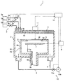
- FIG. 1 is a diagram showing a schematic configuration of a vapor phase growth apparatus 1 according to an embodiment.
- a silicon substrate specifically, a silicon wafer (hereinafter simply referred to as a wafer) W is used as a substrate for film formation, and a plurality of films are stacked on the wafer W.
- a vapor phase growth apparatus 1 in FIG. 1 includes a chamber 2 for forming a film on a wafer W, a gas supply unit 3 for supplying a source gas to the wafer W in the chamber 2, and a source discharge unit located above the chamber 2. 4, a susceptor 5 that supports the wafer W in the chamber 2, a rotating unit 6 that rotates while holding the susceptor 5, a heater 7 that heats the wafer W, a heater driving unit 8 that drives the heater 7, A gas exhaust unit 9 for exhausting the gas in the chamber 2, an exhaust mechanism 10 for exhausting the gas from the gas exhaust unit 9, a radiation thermometer 11 for measuring the temperature of the wafer W, and a control unit 12 for controlling each unit It has.
- the chamber 2 has a shape (for example, a cylindrical shape) that can accommodate the wafer W to be deposited, and the susceptor 5, the heater 7, a part of the rotating unit 6, and the like are accommodated inside the chamber 2.
- the gas supply unit 3 includes a plurality of gas storage units 3a that individually store a plurality of gases, a plurality of gas pipes 3b that connect the gas storage units 3a and the material discharge unit 4, and a gas that flows through the gas pipes 3b. And a plurality of gas valves 3c for adjusting the flow rate of the gas. Each gas valve 3c is connected to a corresponding gas pipe 3b. The plurality of gas valves 3 c are controlled by the control unit 12.
- the actual piping can take a plurality of configurations such as coupling a plurality of gas pipes, branching one gas pipe into a plurality of gas pipes, or combining the branching and coupling of gas pipes.
- the source gas supplied from the gas supply unit 3 is discharged into the chamber 2 through the source discharge unit 4.
- the source gas (process gas) released into the chamber 2 is supplied onto the wafer W, whereby a desired film is formed on the wafer W.
- the kind of source gas to be used is not specifically limited.
- the source gas can be variously changed depending on the type of film to be formed.
- a shower plate 4 a is provided on the bottom surface side of the raw material discharge part 4.
- the shower plate 4a can be configured using a metal material such as stainless steel or an aluminum alloy. Gases from the plurality of gas pipes 3b are mixed in the raw material discharge section 4 and supplied into the chamber 2 through the gas outlet 4b of the shower plate 4a. Note that a plurality of gas flow paths may be provided in the shower plate 4a, and a plurality of types of gases may be supplied to the wafer W in the chamber 2 while being separated.
- the structure of the raw material discharge portion 4 should be selected in consideration of the uniformity of the formed film, the raw material efficiency, the reproducibility, the manufacturing cost, etc., but is not particularly limited as long as these requirements are satisfied.
- the thing of a well-known structure can also be used suitably.
- the susceptor 5 is provided on the upper portion of the rotating unit 6 and has a structure in which the wafer W is placed and supported in a spot facing provided on the inner peripheral side of the susceptor 5.
- the susceptor 5 has an annular shape having an opening at the center thereof, but may have a substantially flat plate shape without an opening.
- the heater 7 is a heating unit that heats the susceptor 5 and / or the wafer W. There is no particular limitation as long as it satisfies requirements such as the ability to heat the object to be heated to a desired temperature and temperature distribution, and durability. Specific examples include resistance heating, lamp heating, and induction heating.
- the heater driving unit 8 supplies a power supply voltage to the heater 7 to flow a current through the heater 7 to heat the heater 7.
- the internal configuration of the heater driving unit 8 will be described later.
- the exhaust mechanism 10 exhausts the reacted raw material gas from the inside of the chamber 2 through the gas exhaust unit 9, and controls the inside of the chamber 2 to a desired pressure by the action of the exhaust valve 10a and the vacuum pump 10b.
- the radiation thermometer 11 is provided on the upper surface of the raw material discharge part 4.
- the radiation thermometer 11 irradiates the wafer W with light from a light source (not shown), receives the reflected light from the wafer W, and measures the reflected light intensity of the wafer W.
- the radiation thermometer 11 receives heat radiation from the film growth surface of the wafer W and measures the heat radiation intensity.
- FIG. 1 only one radiation thermometer 11 is illustrated, but a plurality of radiation thermometers 11 are arranged on the upper surface of the raw material discharge portion 4, so that a plurality of locations (for example, the inner circumference) of the film growth surface of the wafer W are arranged. Side and outer peripheral side) temperatures may be measured.
- a light transmission window is provided on the upper surface of the raw material discharge section 4, and light from the light source of the radiation thermometer 11, reflected light from the wafer W and heat radiation light pass through this light transmission window.
- the light transmission window can take an arbitrary shape such as a slit shape, a rectangular shape, or a circular shape.
- a member transparent to the wavelength range of light measured by the radiation thermometer 11 is used.
- quartz or the like is suitably used as a member of the light transmission window. .
- the control unit 12 includes a computer (not shown) that centrally controls the vapor phase growth apparatus 1 and a storage unit (not shown) that stores a process control program, an apparatus history, and the like.
- the control unit 12 controls the heating mechanism of the gas supply unit 3 and the rotating unit 6, the exhaust mechanism 10, the heating of the wafer W by the heater 7, and the like.
- FIG. 2 is a circuit configuration diagram showing an example of the internal configuration of the heater drive unit 8.
- the heater drive unit 8 in FIG. 2 includes a transformer 21, a primary circuit 22 connected to the primary side of the transformer 21, and a secondary circuit 23 connected to the secondary side of the transformer 21.
- the primary circuit 22 includes a thyristor 24, and a commercial power supply voltage is applied to the primary circuit 22, for example.
- the transformer 21 performs voltage conversion between the AC voltage on the primary circuit 22 side and the AC voltage on the secondary circuit 23 side.
- the heater 7 is connected to the secondary circuit 23.
- a voltmeter 25 and an ammeter 26 are connected to the secondary circuit 23.
- the voltmeter 25 measures the voltage applied to the heater 7, and the ammeter 26 measures the current flowing through the heater 7.
- the measured values of the voltmeter 25 and the ammeter 26 are supplied to the control unit 12.
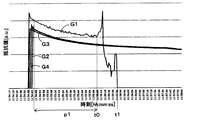
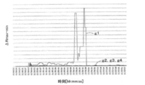
- FIG. 3 is a graph showing the electrical characteristics of the heaters 7 in the four vapor phase growth apparatuses 1.
- the graph G1 in FIG. 3 shows the electrical characteristics of the heater 7 that is completely broken, and the graphs G2 to G4 show the electrical characteristics of the heater 7 that is not broken.
- the horizontal axis represents time [hour minute second]
- the vertical axis represents resistance value [a.u.].
- the resistance value fluctuates with a short period within the period p1 before the time t1, which is considered to be completely broken. Thereafter, from time t0 to t1, the resistance value fluctuates with a larger amplitude in a period longer than the period p1. It is considered that the fracture has progressed considerably after time t0, and in some cases, a part of the constituent material of the heater 7 may start scattering into the chamber 2. Therefore, if the small vibration period of the period p1 before the time t0 can be captured, the heater 7 can be replaced before the constituent material of the heater 7 is scattered in the chamber 2.
- the resistance value of the heater 7 fluctuates greatly and then completely breaks.
- the resistance value of the heater 7 gradually decreases.
- the resistance value of the heater 7 in the period p1 is measured at a plurality of times at a time interval corresponding to a small fluctuation period of the resistance value of the heater 7, and the breakage of the heater 7 is predicted in advance.
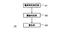
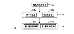
- FIG. 4 is a block diagram showing an example of the internal configuration of the control unit 12.
- the control unit 12 in FIG. 4 includes an electrical characteristic measurement unit 31, a threshold determination unit 32, and a warning unit 33.
- the electrical property measuring unit 31 measures the electrical property of the heater 7 every predetermined time, and detects the fluctuation value of the electrical property.
- the threshold value determination unit 32 determines whether or not the difference between the maximum value and the minimum value of the detected variation value of the predetermined number of electrical characteristics exceeds a predetermined threshold value.
- the warning unit 33 performs warning processing when it is determined that the threshold value is exceeded.
- the electrical characteristics are at least one of a voltage applied to the heater 7, a current flowing through the heater 7, and a resistance value of the heater 7.
- the electrical characteristic measurement unit 31 measures the resistance value of the heater 7 a plurality of times every predetermined time.
- the predetermined time is a time interval corresponding to a small fluctuation cycle of the resistance value of the heater 7 in the period p1 in FIG.
- the electrical characteristic measurement unit 31 detects a fluctuation value from the previously measured resistance value every time the resistance value is measured.
- the threshold determination unit 32 determines whether or not the difference between the maximum value and the minimum value of the fluctuation values for a plurality of times exceeds the threshold.
- the warning unit 33 performs warning processing using, for example, an alarm sound source or a display device (not shown) connected to the control unit 12. For example, an alarm sound source is sounded, and it is notified by voice that the heater 7 is about to break. Alternatively, the display device displays that the heater 7 is about to break.
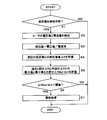
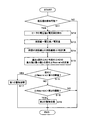
- FIG. 5 is a flowchart showing an example of the processing operation of the control unit 12. This flowchart shows the abnormality detection process of the heater 7 performed by the control unit 12.
- the control unit 12 may perform various processes other than this process, but is omitted in FIG.
- the control unit 12 performs the process of FIG. 5 every predetermined time.
- step S1 it is determined whether or not the resistance value of the heater 7 can be detected. For example, when it is determined that the resistance value of the heater 7 cannot be normally detected due to some factor, the determination process in step S1 is NO, and the process of FIG. 5 ends.
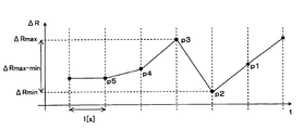
- the electrical characteristic measuring unit 31 calculates a resistance value difference (variation value) ⁇ R from the previously measured resistance value (step S4). If there is no previously measured resistance value, the process of step S4 is omitted.
- the electrical characteristic measuring unit 31 detects a difference ⁇ Rmax-min between the maximum value and the minimum value among the resistance value difference ⁇ R for the past n (for example, 4) times and the resistance value difference ⁇ R calculated this time. (Step S5).
- FIG. 7 is a graph showing an example of calculation results of the resistance value difference between the past four times and this time, with the horizontal axis representing time and the vertical axis representing resistance value difference.
- the five plots p1 in FIG. 7 are the current resistance value differences, and the plots p2 to p5 are the past resistance value differences.
- the difference between the resistance value difference of the plot p2 and the resistance value difference of the plot p3 is ⁇ Rmax-min.
- step S5 The reason why the process of step S5 is provided is to make it possible to reliably detect the resistance value fluctuation of the heater 7 before the heater 7 is completely broken.
- the graphs g1 to g4 after the processing in step S5 are as shown in FIG.
- the horizontal axis of FIG. 6 is time [hour minute second], and the vertical axis is the difference ⁇ Rmax-min between the maximum value and the minimum value of the resistance value difference.
- Graphs g1 to g4 in FIG. 6 correspond to graphs G1 to G4 in FIG. 3, respectively.
- the graph g1 in FIG. 3 corresponds to the broken heater 7, and the difference ⁇ Rmax-min greatly changes before the heater 7 is completely broken. Therefore, it is possible to reliably detect small vibrations before the heater 7 is completely broken.
- the threshold determination unit 32 next determines whether or not the difference ⁇ Rmax-min exceeds a predetermined threshold (step S6). If it exceeds the threshold, the warning unit 33 performs a predetermined warning process (step S7). If the threshold is not exceeded, the processing in FIG. 5 is terminated.
- the resistance value of the heater 7 is measured every predetermined time, the fluctuation value between the newly measured resistance value and the previous resistance value is detected, and the maximum of the fluctuation values for a plurality of times is detected. It is determined whether or not the difference between the value and the minimum value exceeds a threshold value.
- FIG. 8 is a flowchart showing the internal configuration of the control unit 12 according to the second embodiment.
- the control unit 12 of FIG. 8 includes a first determination unit 32 a and a second determination unit 32 b in the threshold determination unit 32.
- the warning unit 33 includes a first warning processing unit 33a and a second warning processing unit 33b.
- the first determination unit 32a determines whether or not the above-described difference ⁇ Rmax-min has exceeded the first threshold value.
- the second determination unit 32b determines whether or not the difference ⁇ Rmax-min has exceeded a second threshold value that is greater than the first threshold value after the first determination unit 32a determines that the first threshold value has been exceeded.
- FIG. 9 is a flowchart showing an example of the processing operation of the control unit 12.
- the processing in steps S11 to S15 is the same as the processing in steps S1 to S5 in FIG.
- the control part 12 performs the process of FIG. 9 for every predetermined time.
- the first determination unit 32a determines whether or not the difference ⁇ Rmax-min exceeds the first threshold value for the first time (step S16). If it is determined that the first threshold is exceeded, the first warning processing unit 33a performs the first warning process (step S17).
- step S16 determines whether or not the difference ⁇ Rmax-min has exceeded a second threshold value that is greater than the first threshold value (step S18). If it is determined that the second threshold value has been exceeded, the second warning processing unit 33b performs a second warning process (step S19).
- first warning process and the second warning process can be considered.
- the method of sounding the alarm sound source or the display content of the display device may be changed.
- the second warning processing unit it is conceivable to perform a ringing or display so that it can be understood that the heater 7 has been nearly broken.
- an alarm sound source or a display device notifies that the heater 7 is about to break, and in the second warning process, in addition to the notification, the heater driving unit 8 is informed to the heater 7.
- a stop process may be performed to stop the power supply.
- the first threshold value is set to detect the period p1 in FIG. 3, and the second threshold value is set to detect the times t0 to t1 in FIG. If the determination in step S18 is no, the process returns to step S11.
- step S19 described above when the difference ⁇ Rmax-min exceeds the second threshold value, the power supply to the heater 7 may be stopped in addition to the warning process, or another type of warning process different from step S17 may be performed. Good.
- the resistance value of the heater 7 is measured every predetermined time, the fluctuation value between the newly measured resistance value and the previous resistance value is detected, and the minimum fluctuation value for a plurality of times is detected. Since the first threshold value and the second threshold value are provided as the threshold values for determining the difference ⁇ Rmax-min between the value and the minimum value, it is possible to notify in detail with two types of warning processing that the heater 7 is about to break. .
- the process of comparing the difference ⁇ Rmax-min in the resistance value of the heater 7 with the threshold value may be performed, but the current flowing through the heater 7 may be compared with the threshold value.
- the abnormality detection method for detecting the breakage of the heater 7 in the vapor phase growth apparatus 1 has been described.
- the heater 7 is not necessarily provided in the vapor phase growth apparatus 1. It is not limited to.
Landscapes
- Chemical & Material Sciences (AREA)
- Engineering & Computer Science (AREA)
- General Chemical & Material Sciences (AREA)
- Chemical Kinetics & Catalysis (AREA)
- Materials Engineering (AREA)
- Metallurgy (AREA)
- Organic Chemistry (AREA)
- Mechanical Engineering (AREA)
- Physics & Mathematics (AREA)
- Condensed Matter Physics & Semiconductors (AREA)
- General Physics & Mathematics (AREA)
- Manufacturing & Machinery (AREA)
- Computer Hardware Design (AREA)
- Microelectronics & Electronic Packaging (AREA)
- Power Engineering (AREA)
- Crystallography & Structural Chemistry (AREA)
- Chemical Vapour Deposition (AREA)
Priority Applications (2)
| Application Number | Priority Date | Filing Date | Title |
|---|---|---|---|
| DE112016004625.1T DE112016004625T5 (de) | 2015-10-08 | 2016-09-30 | Dampfphasenwachstumseinrichtung und Abnormalitätsdetektionsverfahren |
| US15/946,696 US20180291507A1 (en) | 2015-10-08 | 2018-04-05 | Vapor phase growth apparatus and abnormality detection method |
Applications Claiming Priority (2)
| Application Number | Priority Date | Filing Date | Title |
|---|---|---|---|
| JP2015200348A JP2017073498A (ja) | 2015-10-08 | 2015-10-08 | 気相成長装置および異常検出方法 |
| JP2015-200348 | 2015-10-08 |
Related Child Applications (1)
| Application Number | Title | Priority Date | Filing Date |
|---|---|---|---|
| US15/946,696 Continuation US20180291507A1 (en) | 2015-10-08 | 2018-04-05 | Vapor phase growth apparatus and abnormality detection method |
Publications (1)
| Publication Number | Publication Date |
|---|---|
| WO2017061334A1 true WO2017061334A1 (ja) | 2017-04-13 |
Family
ID=58487648
Family Applications (1)
| Application Number | Title | Priority Date | Filing Date |
|---|---|---|---|
| PCT/JP2016/079070 Ceased WO2017061334A1 (ja) | 2015-10-08 | 2016-09-30 | 気相成長装置および異常検出方法 |
Country Status (5)
| Country | Link |
|---|---|
| US (1) | US20180291507A1 (enExample) |
| JP (1) | JP2017073498A (enExample) |
| DE (1) | DE112016004625T5 (enExample) |
| TW (1) | TWI626331B (enExample) |
| WO (1) | WO2017061334A1 (enExample) |
Families Citing this family (1)
| Publication number | Priority date | Publication date | Assignee | Title |
|---|---|---|---|---|
| DE102018101010B4 (de) | 2017-09-25 | 2025-01-09 | X-Fab Semiconductor Foundries Ag | Echtzeit Monitoring eines Mehrzonen-Vertikalofens mit frühzeitiger Erkennung eines Ausfalls eines Heizzonen-Elements |
Citations (3)
| Publication number | Priority date | Publication date | Assignee | Title |
|---|---|---|---|---|
| JP2006165200A (ja) * | 2004-12-06 | 2006-06-22 | Kokusai Electric Semiconductor Service Inc | 半導体製造装置における抵抗加熱ヒータの抵抗値検出装置、半導体製造装置における抵抗加熱ヒータの劣化診断装置及びネットワークシステム |
| JP2009245978A (ja) * | 2008-03-28 | 2009-10-22 | Yokogawa Electric Corp | 半導体製造装置 |
| WO2012165174A1 (ja) * | 2011-06-01 | 2012-12-06 | シャープ株式会社 | 抵抗加熱ヒータの劣化検出装置および方法 |
Family Cites Families (5)
| Publication number | Priority date | Publication date | Assignee | Title |
|---|---|---|---|---|
| JP2002352938A (ja) * | 2001-05-28 | 2002-12-06 | Tokyo Electron Ltd | 熱処理装置のヒ−タ素線の断線予測方法及び熱処理装置 |
| JP3988942B2 (ja) * | 2003-03-31 | 2007-10-10 | 株式会社国際電気セミコンダクターサービス | ヒータ検査装置及びそれを搭載した半導体製造装置 |
| JP4326570B2 (ja) * | 2007-04-17 | 2009-09-09 | 東京エレクトロン株式会社 | ヒータ素線の寿命予測方法,熱処理装置,記録媒体,ヒータ素線の寿命予測処理システム |
| JP4343253B1 (ja) * | 2008-03-27 | 2009-10-14 | Tdk株式会社 | 密閉容器の蓋開閉装置及び該開閉装置を用いたガス置換装置 |
| US8581153B2 (en) * | 2008-09-30 | 2013-11-12 | Tokyo Electron Limited | Method of detecting abnormal placement of substrate, substrate processing method, computer-readable storage medium, and substrate processing apparatus |
-
2015
- 2015-10-08 JP JP2015200348A patent/JP2017073498A/ja active Pending
-
2016
- 2016-09-30 WO PCT/JP2016/079070 patent/WO2017061334A1/ja not_active Ceased
- 2016-09-30 DE DE112016004625.1T patent/DE112016004625T5/de not_active Ceased
- 2016-10-05 TW TW105132122A patent/TWI626331B/zh active
-
2018
- 2018-04-05 US US15/946,696 patent/US20180291507A1/en not_active Abandoned
Patent Citations (3)
| Publication number | Priority date | Publication date | Assignee | Title |
|---|---|---|---|---|
| JP2006165200A (ja) * | 2004-12-06 | 2006-06-22 | Kokusai Electric Semiconductor Service Inc | 半導体製造装置における抵抗加熱ヒータの抵抗値検出装置、半導体製造装置における抵抗加熱ヒータの劣化診断装置及びネットワークシステム |
| JP2009245978A (ja) * | 2008-03-28 | 2009-10-22 | Yokogawa Electric Corp | 半導体製造装置 |
| WO2012165174A1 (ja) * | 2011-06-01 | 2012-12-06 | シャープ株式会社 | 抵抗加熱ヒータの劣化検出装置および方法 |
Also Published As
| Publication number | Publication date |
|---|---|
| TW201723218A (zh) | 2017-07-01 |
| TWI626331B (zh) | 2018-06-11 |
| US20180291507A1 (en) | 2018-10-11 |
| DE112016004625T5 (de) | 2018-06-21 |
| JP2017073498A (ja) | 2017-04-13 |
Similar Documents
| Publication | Publication Date | Title |
|---|---|---|
| JP4326570B2 (ja) | ヒータ素線の寿命予測方法,熱処理装置,記録媒体,ヒータ素線の寿命予測処理システム | |
| KR101182502B1 (ko) | 기판의 이상 배치 상태의 검지 방법, 기판 처리 방법, 컴퓨터 판독 가능한 기억 매체 및 기판 처리 장치 | |
| TWI676017B (zh) | 加熱管之氣體洩漏檢測裝置及加熱管之氣體洩漏檢測方法 | |
| US20200367320A1 (en) | Plasma processing apparatus and temperature control method | |
| US9570337B2 (en) | Film formation apparatus and film formation method | |
| JP4420356B2 (ja) | ヒータ素線の寿命予測方法,熱処理装置,記録媒体,ヒータ素線の寿命予測処理システム | |
| WO2017061334A1 (ja) | 気相成長装置および異常検出方法 | |
| KR102201063B1 (ko) | 히터 온도 변화를 이용한 히터 이상 여부 판단 장치 및 그 방법 | |
| JP2011151055A (ja) | 温度測定方法及び基板処理装置 | |
| EP4379782A1 (en) | Heater life prediction method, heat treatment apparatus, and heater life prediction program | |
| JP6272743B2 (ja) | 基板処理装置 | |
| TWI729274B (zh) | 成膜裝置與成膜方法 | |
| US12417890B2 (en) | Methods, systems, and apparatus for monitoring radiation output of lamps | |
| JP2017017251A (ja) | 気相成長装置および温度検出方法 | |
| JP2019106462A (ja) | 気相成長装置及び温度測定方法 | |
| KR20160094057A (ko) | 반응 챔버의 히터 단선 감지시스템 및 방법 | |
| KR102900018B1 (ko) | 히터 제어 장치 | |
| JP2014063820A (ja) | 基板処理装置、基板処理方法及び半導体装置の製造方法 | |
| JP7494946B2 (ja) | ヒータ制御装置 | |
| KR20140011712A (ko) | 증발장치 | |
| KR102452021B1 (ko) | 온도 감시 장치, 열처리 장치 및 온도 감시 방법 | |
| KR101288055B1 (ko) | 셀프 플라즈마 챔버를 포함하는 공정진행 모니터링 장치 | |
| JP2017190506A (ja) | 気相成長装置および気相成長方法 |
Legal Events
| Date | Code | Title | Description |
|---|---|---|---|
| 121 | Ep: the epo has been informed by wipo that ep was designated in this application |
Ref document number: 16853488 Country of ref document: EP Kind code of ref document: A1 |
|
| WWE | Wipo information: entry into national phase |
Ref document number: 112016004625 Country of ref document: DE |
|
| 122 | Ep: pct application non-entry in european phase |
Ref document number: 16853488 Country of ref document: EP Kind code of ref document: A1 |