WO2017051775A1 - ペースト組成物及びシリコンゲルマニウム層の形成方法 - Google Patents
ペースト組成物及びシリコンゲルマニウム層の形成方法 Download PDFInfo
- Publication number
- WO2017051775A1 WO2017051775A1 PCT/JP2016/077439 JP2016077439W WO2017051775A1 WO 2017051775 A1 WO2017051775 A1 WO 2017051775A1 JP 2016077439 W JP2016077439 W JP 2016077439W WO 2017051775 A1 WO2017051775 A1 WO 2017051775A1
- Authority
- WO
- WIPO (PCT)
- Prior art keywords
- silicon
- aluminum
- paste composition
- mass
- layer
- Prior art date
- Legal status (The legal status is an assumption and is not a legal conclusion. Google has not performed a legal analysis and makes no representation as to the accuracy of the status listed.)
- Ceased
Links
Images


Classifications
-
- C—CHEMISTRY; METALLURGY
- C09—DYES; PAINTS; POLISHES; NATURAL RESINS; ADHESIVES; COMPOSITIONS NOT OTHERWISE PROVIDED FOR; APPLICATIONS OF MATERIALS NOT OTHERWISE PROVIDED FOR
- C09D—COATING COMPOSITIONS, e.g. PAINTS, VARNISHES OR LACQUERS; FILLING PASTES; CHEMICAL PAINT OR INK REMOVERS; INKS; CORRECTING FLUIDS; WOODSTAINS; PASTES OR SOLIDS FOR COLOURING OR PRINTING; USE OF MATERIALS THEREFOR
- C09D1/00—Coating compositions, e.g. paints, varnishes or lacquers, based on inorganic substances
-
- H—ELECTRICITY
- H10—SEMICONDUCTOR DEVICES; ELECTRIC SOLID-STATE DEVICES NOT OTHERWISE PROVIDED FOR
- H10P—GENERIC PROCESSES OR APPARATUS FOR THE MANUFACTURE OR TREATMENT OF DEVICES COVERED BY CLASS H10
- H10P14/00—Formation of materials, e.g. in the shape of layers or pillars
- H10P14/20—Formation of materials, e.g. in the shape of layers or pillars of semiconductor materials
- H10P14/29—Formation of materials, e.g. in the shape of layers or pillars of semiconductor materials characterised by the substrates
- H10P14/2901—Materials
- H10P14/2902—Materials being Group IVA materials
- H10P14/2905—Silicon, silicon germanium or germanium
-
- B—PERFORMING OPERATIONS; TRANSPORTING
- B05—SPRAYING OR ATOMISING IN GENERAL; APPLYING FLUENT MATERIALS TO SURFACES, IN GENERAL
- B05D—PROCESSES FOR APPLYING FLUENT MATERIALS TO SURFACES, IN GENERAL
- B05D3/00—Pretreatment of surfaces to which liquids or other fluent materials are to be applied; After-treatment of applied coatings, e.g. intermediate treating of an applied coating preparatory to subsequent applications of liquids or other fluent materials
- B05D3/02—Pretreatment of surfaces to which liquids or other fluent materials are to be applied; After-treatment of applied coatings, e.g. intermediate treating of an applied coating preparatory to subsequent applications of liquids or other fluent materials by baking
- B05D3/0254—After-treatment
-
- B—PERFORMING OPERATIONS; TRANSPORTING
- B05—SPRAYING OR ATOMISING IN GENERAL; APPLYING FLUENT MATERIALS TO SURFACES, IN GENERAL
- B05D—PROCESSES FOR APPLYING FLUENT MATERIALS TO SURFACES, IN GENERAL
- B05D7/00—Processes, other than flocking, specially adapted for applying liquids or other fluent materials to particular surfaces or for applying particular liquids or other fluent materials
- B05D7/24—Processes, other than flocking, specially adapted for applying liquids or other fluent materials to particular surfaces or for applying particular liquids or other fluent materials for applying particular liquids or other fluent materials
-
- B—PERFORMING OPERATIONS; TRANSPORTING
- B05—SPRAYING OR ATOMISING IN GENERAL; APPLYING FLUENT MATERIALS TO SURFACES, IN GENERAL
- B05D—PROCESSES FOR APPLYING FLUENT MATERIALS TO SURFACES, IN GENERAL
- B05D7/00—Processes, other than flocking, specially adapted for applying liquids or other fluent materials to particular surfaces or for applying particular liquids or other fluent materials
- B05D7/50—Multilayers
- B05D7/56—Three layers or more
- B05D7/58—No clear coat specified
- B05D7/584—No clear coat specified at least some layers being let to dry, at least partially, before applying the next layer
-
- H—ELECTRICITY
- H01—ELECTRIC ELEMENTS
- H01B—CABLES; CONDUCTORS; INSULATORS; SELECTION OF MATERIALS FOR THEIR CONDUCTIVE, INSULATING OR DIELECTRIC PROPERTIES
- H01B1/00—Conductors or conductive bodies characterised by the conductive materials; Selection of materials as conductors
- H01B1/20—Conductive material dispersed in non-conductive organic material
- H01B1/22—Conductive material dispersed in non-conductive organic material the conductive material comprising metals or alloys
-
- H—ELECTRICITY
- H10—SEMICONDUCTOR DEVICES; ELECTRIC SOLID-STATE DEVICES NOT OTHERWISE PROVIDED FOR
- H10P—GENERIC PROCESSES OR APPARATUS FOR THE MANUFACTURE OR TREATMENT OF DEVICES COVERED BY CLASS H10
- H10P14/00—Formation of materials, e.g. in the shape of layers or pillars
- H10P14/20—Formation of materials, e.g. in the shape of layers or pillars of semiconductor materials
-
- H—ELECTRICITY
- H10—SEMICONDUCTOR DEVICES; ELECTRIC SOLID-STATE DEVICES NOT OTHERWISE PROVIDED FOR
- H10P—GENERIC PROCESSES OR APPARATUS FOR THE MANUFACTURE OR TREATMENT OF DEVICES COVERED BY CLASS H10
- H10P14/00—Formation of materials, e.g. in the shape of layers or pillars
- H10P14/20—Formation of materials, e.g. in the shape of layers or pillars of semiconductor materials
- H10P14/26—Formation of materials, e.g. in the shape of layers or pillars of semiconductor materials using liquid deposition
- H10P14/263—Formation of materials, e.g. in the shape of layers or pillars of semiconductor materials using liquid deposition using melted materials
-
- H—ELECTRICITY
- H10—SEMICONDUCTOR DEVICES; ELECTRIC SOLID-STATE DEVICES NOT OTHERWISE PROVIDED FOR
- H10P—GENERIC PROCESSES OR APPARATUS FOR THE MANUFACTURE OR TREATMENT OF DEVICES COVERED BY CLASS H10
- H10P14/00—Formation of materials, e.g. in the shape of layers or pillars
- H10P14/20—Formation of materials, e.g. in the shape of layers or pillars of semiconductor materials
- H10P14/26—Formation of materials, e.g. in the shape of layers or pillars of semiconductor materials using liquid deposition
- H10P14/265—Formation of materials, e.g. in the shape of layers or pillars of semiconductor materials using liquid deposition using solutions
-
- H—ELECTRICITY
- H10—SEMICONDUCTOR DEVICES; ELECTRIC SOLID-STATE DEVICES NOT OTHERWISE PROVIDED FOR
- H10P—GENERIC PROCESSES OR APPARATUS FOR THE MANUFACTURE OR TREATMENT OF DEVICES COVERED BY CLASS H10
- H10P14/00—Formation of materials, e.g. in the shape of layers or pillars
- H10P14/20—Formation of materials, e.g. in the shape of layers or pillars of semiconductor materials
- H10P14/34—Deposited materials, e.g. layers
- H10P14/3402—Deposited materials, e.g. layers characterised by the chemical composition
- H10P14/3404—Deposited materials, e.g. layers characterised by the chemical composition being Group IVA materials
- H10P14/3411—Silicon, silicon germanium or germanium
-
- H—ELECTRICITY
- H10—SEMICONDUCTOR DEVICES; ELECTRIC SOLID-STATE DEVICES NOT OTHERWISE PROVIDED FOR
- H10P—GENERIC PROCESSES OR APPARATUS FOR THE MANUFACTURE OR TREATMENT OF DEVICES COVERED BY CLASS H10
- H10P14/00—Formation of materials, e.g. in the shape of layers or pillars
- H10P14/20—Formation of materials, e.g. in the shape of layers or pillars of semiconductor materials
- H10P14/34—Deposited materials, e.g. layers
- H10P14/3438—Doping during depositing
- H10P14/3441—Conductivity type
- H10P14/3444—P-type
-
- H—ELECTRICITY
- H10—SEMICONDUCTOR DEVICES; ELECTRIC SOLID-STATE DEVICES NOT OTHERWISE PROVIDED FOR
- H10P—GENERIC PROCESSES OR APPARATUS FOR THE MANUFACTURE OR TREATMENT OF DEVICES COVERED BY CLASS H10
- H10P14/00—Formation of materials, e.g. in the shape of layers or pillars
- H10P14/20—Formation of materials, e.g. in the shape of layers or pillars of semiconductor materials
- H10P14/34—Deposited materials, e.g. layers
- H10P14/3451—Structure
- H10P14/3452—Microstructure
-
- H—ELECTRICITY
- H10—SEMICONDUCTOR DEVICES; ELECTRIC SOLID-STATE DEVICES NOT OTHERWISE PROVIDED FOR
- H10P—GENERIC PROCESSES OR APPARATUS FOR THE MANUFACTURE OR TREATMENT OF DEVICES COVERED BY CLASS H10
- H10P14/00—Formation of materials, e.g. in the shape of layers or pillars
- H10P14/20—Formation of materials, e.g. in the shape of layers or pillars of semiconductor materials
- H10P14/38—Formation of materials, e.g. in the shape of layers or pillars of semiconductor materials characterised by treatments done after the formation of the materials
- H10P14/3802—Crystallisation or recrystallisation of non-monocrystalline semiconductor materials, e.g. regrowth
-
- H—ELECTRICITY
- H10—SEMICONDUCTOR DEVICES; ELECTRIC SOLID-STATE DEVICES NOT OTHERWISE PROVIDED FOR
- H10P—GENERIC PROCESSES OR APPARATUS FOR THE MANUFACTURE OR TREATMENT OF DEVICES COVERED BY CLASS H10
- H10P95/00—Generic processes or apparatus for manufacture or treatments not covered by the other groups of this subclass
- H10P95/90—Thermal treatments, e.g. annealing or sintering
-
- H—ELECTRICITY
- H10—SEMICONDUCTOR DEVICES; ELECTRIC SOLID-STATE DEVICES NOT OTHERWISE PROVIDED FOR
- H10W—GENERIC PACKAGES, INTERCONNECTIONS, CONNECTORS OR OTHER CONSTRUCTIONAL DETAILS OF DEVICES COVERED BY CLASS H10
- H10W72/00—Interconnections or connectors in packages
- H10W72/01—Manufacture or treatment
- H10W72/013—Manufacture or treatment of die-attach connectors
-
- H—ELECTRICITY
- H10—SEMICONDUCTOR DEVICES; ELECTRIC SOLID-STATE DEVICES NOT OTHERWISE PROVIDED FOR
- H10W—GENERIC PACKAGES, INTERCONNECTIONS, CONNECTORS OR OTHER CONSTRUCTIONAL DETAILS OF DEVICES COVERED BY CLASS H10
- H10W72/00—Interconnections or connectors in packages
- H10W72/30—Die-attach connectors
-
- B—PERFORMING OPERATIONS; TRANSPORTING
- B05—SPRAYING OR ATOMISING IN GENERAL; APPLYING FLUENT MATERIALS TO SURFACES, IN GENERAL
- B05D—PROCESSES FOR APPLYING FLUENT MATERIALS TO SURFACES, IN GENERAL
- B05D2203/00—Other substrates
- B05D2203/30—Other inorganic substrates, e.g. ceramics, silicon
Definitions
- the present invention relates to a paste composition and a method for forming a silicon germanium layer.
- silicon germanium which is a mixed crystal material of silicon and germanium, is used as one of semiconductor materials.
- Such a semiconductor material is formed as a silicon germanium layer on a substrate such as silicon and used as a part of a transistor or a diode.
- Patent Document 1 As a method for forming a silicon germanium layer, a method of performing epitaxial growth by chemical vapor deposition (CVD) (see Patent Document 1), a method of performing epitaxial growth by molecular beam epitaxy (MBE), or (see Patent Document 2), Si A method of forming a film by sputtering using a -Ge based alloy target is disclosed (see Patent Document 3).
- CVD chemical vapor deposition
- MBE molecular beam epitaxy
- Patent Document 2 Si A method of forming a film by sputtering using a -Ge based alloy target is disclosed (see Patent Document 3).
- Patent Documents 1 and 2 have a problem that it is necessary to use a gas with high risk such as SiH 4 or GeH 4 .
- Patent Documents 1 to 3 have a problem that a long time is required for these steps because a vacuum apparatus is required in the step of performing epitaxial growth and the step of forming a film by sputtering.
- the present invention provides a paste composition capable of forming a silicon germanium layer safely and easily, and formation of a silicon germanium layer capable of forming a silicon germanium layer safely and easily. It aims to provide a method.
- the present invention relates to the following paste composition and method for forming a silicon germanium layer.
- a paste composition for forming a silicon germanium layer A paste composition comprising aluminum and germanium, wherein the germanium content is more than 1 part by mass and 10000 parts by mass or less with respect to 100 parts by mass of the aluminum.
- the paste composition according to Item 1 further comprising a resin component.
- the paste composition according to Item 2 wherein the content of the resin component is 0.1 to 10 parts by mass with respect to 100 parts by mass of the aluminum. 4).
- a method for forming a silicon germanium layer comprising: (1) Step 1 of applying a paste composition containing aluminum and germanium on a silicon-containing substrate, wherein the germanium content is more than 1 part by mass and less than 10,000 parts by mass with respect to 100 parts by mass of the aluminum. And (2) Step 2 of firing the substrate coated with the paste composition A forming method characterized by comprising: 7).
- Item 7 The forming method according to Item 6, wherein the baking is performed at a temperature of 500 to 1000 ° C.
- the paste composition of the present invention contains aluminum and germanium, and the germanium content is a specific range of content relative to aluminum.
- a silicon germanium layer can be easily formed.
- the silicon germanium layer forming method of the present invention can form a silicon germanium layer safely and easily because a silicon germanium layer can be formed by applying a paste composition on a substrate and heating it. can do.
- the paste composition of the present invention is a paste composition for forming a silicon germanium layer, and contains aluminum and germanium.
- the germanium content exceeds 1 part by mass with respect to 100 parts by mass of the aluminum, It is 10,000 parts by mass or less.
- the paste composition of the present invention has the above-described configuration, and is applied to a silicon-containing substrate such as a silicon wafer by a coating method such as screen printing, and heated, whereby silicon contained in the silicon-containing substrate and paste
- a silicon-containing substrate such as a silicon wafer
- a coating method such as screen printing
- the alloy recrystallizes and a silicon germanium layer is formed on the silicon-containing substrate.
- the silicon germanium layer can be formed by applying the paste composition of the present invention on a silicon-containing substrate and heating, it is necessary to use a gas with high risk such as SiH 4 or GeH 4.
- a silicon germanium layer can be formed safely and easily without requiring a long time.
- the paste composition of the present invention is a paste composition for forming a silicon germanium layer, and contains aluminum and germanium, and the germanium content is 1 part by mass with respect to 100 parts by mass of the aluminum. And 10000 parts by mass or less.
- aluminum As aluminum, it will not specifically limit if it is a form which can be contained in a paste composition, For example, aluminum powder is mentioned.
- the aluminum powder preferably has an aluminum content of 99.0% by mass or more, and more preferably 99.9% by mass or more.
- the aluminum powder may be an aluminum alloy powder containing another metal in addition to aluminum.
- the aluminum alloy powder include an alloy powder containing at least one element selected from the group consisting of iron, copper, manganese, magnesium, chromium, zinc, titanium, vanadium, gallium, nickel, boron, and zirconium. Is done.
- the content of each of these elements is preferably 1000 ppm or less, particularly 300 ppm or less, based on the total amount of the aluminum alloy powder.
- the shape of the aluminum powder is not particularly limited, and may be any shape such as a spherical shape, an elliptical shape, an indefinite shape, a scale shape, and a fibrous shape. Among these, a spherical shape is preferable in terms of good printability and excellent reactivity with silicon.
- the average particle diameter (D 50 ) of the aluminum powder is preferably 1 to 20 ⁇ m, more preferably 1 to 10 ⁇ m, still more preferably 1 to 5 ⁇ m.
- the average particle diameter of the aluminum powder is within the above range, the aluminum powder is more excellent in reactivity with silicon, and the printability of the paste composition is improved.
- the average particle diameter (D 50 ) is a value measured by a laser diffraction method, and specifically obtained by determining the particle diameter and the number of particles corresponding to this particle diameter. The particle diameter of the particles corresponding to the 50th of the total number of particles in the obtained particle size distribution curve is shown.
- the content of aluminum in the paste composition is not particularly limited, but is preferably 5 to 80% by mass, more preferably 6 to 65% by mass, based on 100% by mass of the paste composition.
- the content of aluminum is in the above range, the reactivity between aluminum and silicon is more excellent, thereby improving the reactivity of germanium with silicon and forming a silicon germanium layer more easily. .
- germanium is not particularly limited as long as it can be contained in the paste composition, and examples thereof include germanium powder.
- the germanium powder preferably has a germanium purity of 98.0% by mass or more.
- the germanium powder may be a germanium alloy powder containing another metal in addition to germanium.
- Examples of the germanium alloy powder include an alloy powder containing at least one element selected from the group consisting of iron, copper, manganese, magnesium, chromium, zinc, titanium, vanadium, gallium, nickel, boron, and zirconium. Is done.
- the content of each of these elements is preferably 1000 ppm by mass or less, particularly preferably 300 ppm by mass or less, based on the total amount of germanium alloy powder.
- the shape of the germanium powder is not particularly limited, and may be any shape such as a spherical shape, an elliptical shape, an indefinite shape, a scale shape, and a fibrous shape. Among these, a spherical shape is preferable in terms of good printability and excellent reactivity with silicon.
- the average particle diameter (D 50 ) of the germanium powder is preferably 1 to 20 ⁇ m, more preferably 1 to 10 ⁇ m, still more preferably 1 to 5 ⁇ m.
- the average particle diameter of the germanium powder is within the above range, the germanium powder is more excellent in reactivity with silicon, and the printability of the paste composition is improved.
- Germanium content exceeds 1 part by mass with respect to 100 parts by mass of aluminum and is 10000 parts by mass or less.
- a silicon germanium layer is not formed as content of germanium is 1 mass part or less.
- the content of the germanium is preferably 50 parts by mass or more, and more preferably 100 parts by mass or more.
- the germanium content is preferably 10000 parts by mass or less, and more preferably 5000 parts by mass or less.
- the paste composition of the present invention may contain a glass component.
- the reactivity between aluminum and silicon is more excellent, thereby improving the reactivity of germanium with silicon and forming a silicon germanium layer more easily. .
- the glass component preferably contains at least one of alkali metals and alkaline earth metals. Specifically, it is preferable to include at least one oxide of lithium, sodium, potassium belonging to an alkali metal, and calcium, magnesium, strontium, and barium belonging to an alkaline earth metal. Further, the glass component may contain one or more selected from the group consisting of Pb, Bi, V, B, Si, Sn, P, and Zn. Furthermore, lead-containing glass components, or lead-free glass components such as bismuth, vanadium, tin-phosphorus, zinc borosilicate, and alkali borosilicate can be used. In view of the influence on the human body, it is desirable to use a lead-free glass component.
- the glass component preferably has a softening point of 300 to 700 ° C, more preferably 400 to 600 ° C.
- the softening point of the glass component is in the above range, the reaction between aluminum and silicon is further promoted, thereby improving the reactivity of germanium with silicon and forming a silicon germanium layer more easily.
- the glass component is not particularly limited as long as it can be contained in the paste composition, and examples thereof include glass powder.
- the average particle diameter of the glass powder is preferably 1 to 8 ⁇ m, more preferably 2 to 4 ⁇ m. If the average particle size of the glass powder is too small, the glass powder may aggregate when the paste is dispersed, and if it is too large, the formation of the silicon germanium layer may be hindered.
- the content of the glass component is not particularly limited, but is preferably 0.1 to 3 parts by mass, and more preferably 0.1 to 1 part by mass with respect to 100 parts by mass of aluminum and germanium.
- the content of the glass component is within the above range, the reactivity between aluminum and silicon is more excellent, thereby improving the reactivity of germanium with silicon and forming a silicon germanium layer more easily. it can.
- the paste composition of the present invention may contain a resin component.
- the stability and printability of the paste composition can be improved.
- Resin used as the resin component is not particularly limited, and conventionally known resins can be used.
- resins include ethyl cellulose, nitrocellulose, polyvinyl butyral, phenol resin, melanin resin, urea resin, xylene resin, alkyd resin, unsaturated polyester resin, acrylic resin, polyimide resin, furan resin, urethane resin, isocyanate compound , Thermosetting resins such as cyanate compounds, polyethylene, polypropylene, polystyrene, ABS resin, polymethyl methacrylate, polyvinyl chloride, polyvinylidene chloride, polyvinyl acetate, polyvinyl alcohol, polyacetal, polycarbonate, polyethylene terephthalate, polybutylene terephthalate, polyphenylene Oxide, Polysulfone, Polyimide, Polyethersulfone, Polyarylate, Polyetheretherketone, Polytetrafluoroethylene Ethylene, silicone resins and the like.
- the melting point of the resin component is preferably 100 to 300 ° C, more preferably 150 to 300 ° C.
- the reaction of aluminum with silicon is further promoted, whereby the reactivity of germanium with silicon is improved, and a silicon germanium layer can be formed more easily.
- the content of the resin component is not particularly limited, but is preferably 0.1 to 10 parts by mass, more preferably 0.5 to 7.5 parts by mass with respect to 100 parts by mass of aluminum. When the content of the resin component is in the above range, the stability and printability of the paste composition can be improved.
- the paste composition of the present invention may contain a dispersion medium.
- the paste composition contains a dispersion medium, the printability of the paste composition can be improved.
- the dispersion medium is not particularly limited as long as aluminum and germanium can be dispersed, and water, a solvent, and the like can be used.
- the paste composition of the present invention may be in a form in which aluminum and germanium are dispersed in water and / or a solvent, or in a form containing an organic vehicle in which the resin component is dissolved in aluminum, germanium, and a solvent. There may be.
- solvent known solvents can be used, and specific examples include diethylene glycol monobutyl ether, diethylene glycol monobutyl ether acetate, dipropylene glycol monomethyl ether, and terpineol. Among these, diethylene glycol monobutyl ether and terpineol are preferable in terms of dispersibility and printability.
- These dispersion media may be used alone or in combination of two or more.
- the content of the dispersion medium is not particularly limited, but is preferably 1 to 30% by mass and more preferably 5 to 15% by mass with respect to 100% by mass of the paste composition. When the content of the dispersion medium is in the above range, the stability and printability of the paste composition are further improved.
- the paste composition of the present invention may contain other additives in addition to the aluminum, germanium, glass component, resin component and dispersion medium.
- additives are not particularly limited as long as the effects of the present invention are not hindered.
- antioxidants corrosion inhibitors, antifoaming agents, thickeners (tackfires), coupling agents, and electrostatic imparting agents.
- Polymerization inhibitors Polymerization inhibitors, thixotropic agents, anti-settling agents and the like.
- polyethylene glycol ester compound polyoxyethylene sorbitan ester compound, sorbitan alkyl ester compound, aliphatic polycarboxylic acid compound, phosphate ester compound, amide amine salt of polyester acid, polyethylene oxide compound, fatty acid amide Wax etc.
- polyethylene glycol ester compound polyoxyethylene sorbitan ester compound, sorbitan alkyl ester compound, aliphatic polycarboxylic acid compound, phosphate ester compound, amide amine salt of polyester acid, polyethylene oxide compound, fatty acid amide Wax etc.
- the content of other additives is not particularly limited, and is preferably about 0.01 to 2 parts by mass with respect to 100 parts by mass of aluminum.
- the viscosity of the paste composition of the present invention is preferably 5 to 100 Pa ⁇ s, more preferably 10 to 40 Pa ⁇ s.
- the viscosity of the paste composition is in the above range, the paste composition is excellent in printability.
- the above viscosity is a value measured under the condition of a rotational speed of 2.5 rpm with a spindle CP-51 using a rotational viscometer (Brookfield, Inc .: DV2T). *
- the method for producing the paste composition of the present invention is not particularly limited, and each component may be stirred and mixed by a conventionally known method.
- each component may be stirred and mixed by a conventionally known method.
- it can be produced by a production method in which aluminum and germanium are added to the dispersion medium, and a glass component, a resin component and other additives are added as necessary, and the mixture is stirred and mixed at room temperature.
- the method for forming a silicon germanium layer of the present invention is a method having the following steps 1 and 2.
- (2) firing the silicon-containing substrate coated with the paste composition 2 A forming method characterized by comprising: Details will be described below.
- Step 1 is a step of applying a paste composition containing aluminum and germanium on a silicon-containing substrate, wherein the germanium content is more than 1 part by mass and not more than 10000 parts by mass with respect to 100 parts by mass of the aluminum. It is.
- the paste composition described above can be used.
- the silicon-containing substrate is not particularly limited as long as it contains silicon, and examples thereof include a silicon substrate.
- a silicon substrate a substrate obtained by slicing a silicon ingot can be used.
- the silicon substrate preferably has a silicon content of 99.0% by mass or more, more preferably 99.99% by mass or more.
- the silicon substrate may contain elements other than silicon as impurities or additives.
- elements other than silicon include boron, phosphorus, gallium, aluminum, or silicon ingot, which are dopants to the semiconductor, and oxygen, nitrogen, carbon, iron, and the like included in the manufacturing process.
- concentration of other elements is preferably 100 ppm or less.
- the thickness of the silicon-containing substrate is preferably 50 to 600 ⁇ m, more preferably 150 to 300 ⁇ m.
- the coating method for coating the paste composition on the silicon-containing substrate is not particularly limited, and examples thereof include a coating method such as spin coating and ink jet printing.
- examples of the coating method include dip coating or a known roll coating method.
- air doctor coating, blade coating, rod coating, extrusion coating, air knife coating examples thereof include a squeeze coat, an impregnated coat, a reverse roll coat, a transfer roll coat, a gravure coat, a kiss coat, a cast coat, and a spray coat.
- Examples of the coating method include a printing method in which the optimum viscosity region is in a relatively low viscosity region, such as intaglio printing, and a printing method in which the optimum viscosity region is in a relatively high viscosity region, such as screen printing.
- a printing method in which the optimum viscosity region is in a relatively low viscosity region such as intaglio printing
- a printing method in which the optimum viscosity region is in a relatively high viscosity region such as screen printing.
- stencil printing method, intaglio printing method, lithographic printing method and the like can be mentioned.
- the coating amount of the paste composition to the silicon-containing substrate is preferably 4 ⁇ 12mg / cm 2, more preferably 6 ⁇ 8mg / cm 2.
- the paste composition is applied onto the silicon-containing substrate.
- Step 2 is a step of firing the silicon-containing substrate coated with the paste composition.
- Calcination conditions are not limited, but the calcination can be performed in an air atmosphere or an inert gas atmosphere such as nitrogen.
- Calcination temperature is preferably 500 to 1000 ° C, more preferably 600 to 1000 ° C, and further preferably 850 to 950 ° C. By firing at a firing temperature within the above range, a silicon germanium layer is sufficiently formed.
- the firing time is preferably 3 to 600 seconds, more preferably 5 to 300 seconds. By setting the firing time within the above range, the silicon germanium layer is sufficiently formed.
- the firing time may be adjusted according to the firing temperature. However, it is preferable to increase the firing temperature and shorten the firing time in terms of excellent production efficiency.
- the evacuation process requires 5 minutes or more, and further, a silicon germanium layer is formed for several minutes to several hours depending on the thickness of the film to be formed.
- the silicon germanium layer formation method of the present invention does not require a vacuum device, and can form a silicon germanium layer within a baking time in the above range.
- the alloy After the firing step, when the temperature is lowered, the alloy is recrystallized and a silicon germanium layer is formed on the silicon-containing substrate. In step 2, it may be cooled after firing.
- the cooling rate at the time of cooling is preferably 1 to 30 ° C./s, and more preferably 10 to 20 ° C./s.
- the method for forming a silicon germanium layer of the present invention includes a preheating step for removing a resin component or the like from the paste composition applied on a silicon-containing substrate between the step 1 and the step 2. May be.
- a preheating step for removing a resin component or the like from the paste composition applied on a silicon-containing substrate between the step 1 and the step 2. May be.
- the preheating condition is not limited, but it may be preheated by heating by a conventionally known method in an air atmosphere or an inert gas atmosphere such as nitrogen.
- the preheating temperature is preferably 300 to 500 ° C, more preferably 400 to 500 ° C.
- the preheating time is preferably 20 to 600 seconds, and more preferably 20 to 60 seconds.
- the method for forming a silicon germanium layer of the present invention may have a drying step of drying the paste composition applied on the silicon-containing substrate before the preheating step.
- the drying step By having the drying step, the dispersion medium present in the paste composition can be removed to some extent in advance, and the silicon germanium layer can be more sufficiently formed.
- Drying conditions are not limited, but it may be dried by heating by a conventionally known method in an air atmosphere or an inert gas atmosphere such as nitrogen.
- the drying temperature is preferably 100 to 400 ° C, more preferably 100 to 200 ° C.
- the drying time is preferably 20 to 600 seconds, more preferably 60 to 300 seconds.
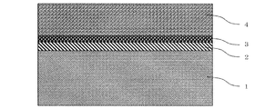
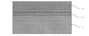
- a silicon germanium layer is formed on the silicon-containing substrate as shown in FIG.
- FIGS. 1 and 2 are schematic cross-sectional views showing an example of the state after performing steps 1 and 2.
- a silicon germanium layer (Si—Ge layer) 2 is formed on a silicon-containing substrate 1.
- an aluminum-silicon germanium layer (Al—Si—Ge layer) 3 and an aluminum germanium sintered body layer (Al—Ge sintered body layer) 4 are further formed as unnecessary layers. Yes.
- a silicon germanium layer (Si—Ge layer) 2 is formed on the silicon-containing substrate 1.
- an aluminum germanium sintered body layer (Al—Ge sintered body layer) 4 is further formed as an unnecessary layer.
- the layer structure after performing Steps 1 and 2 is an aluminum-silicon germanium layer (Al—Si—Ge layer) 3 and an aluminum germanium sintered body layer (Al—Ge layer) on the silicon germanium layer 2 as shown in FIG. Or a layer in which an aluminum germanium sintered body layer (Al—Ge sintered body layer) 4 is formed on the silicon germanium layer 2 as shown in FIG. Whether it becomes a structure changes with conditions, such as the ratio of the aluminum and germanium in a paste composition, the calcination temperature of the process 2.
- the method for forming a silicon germanium layer according to the present invention includes the aluminum-silicon germanium layer (Al-Si-Ge layer) and the aluminum germanium sintered body layer formed on the silicon germanium layer in step 2 after step 2 above. You may have the process of removing unnecessary layers, such as (Al-Ge sintered compact layer).
- the method for removing the unnecessary layer is not particularly limited, and may be removed by a conventionally known method. Examples of such a method include etching with acid or alkali; polishing with abrasive cloth; polishing with silicon oxide abrasive grains, aluminum oxide abrasive grains, diamond abrasive grains, and the like.
- Example 1 The following raw materials were prepared.
- Aluminum powder manufactured by Toyo Aluminum Co., Ltd .; spherical powder with aluminum content of 99.9% by mass Average particle size: 4 ⁇ m
- Germanium powder Ge Powder (manufactured by Furuuchi Chemical Co., Ltd .; non-spherical powder having a germanium content of 99.999% by mass, average particle diameter of 10 ⁇ m)
- Resin component ethyl cellulose resin (manufactured by Dow)
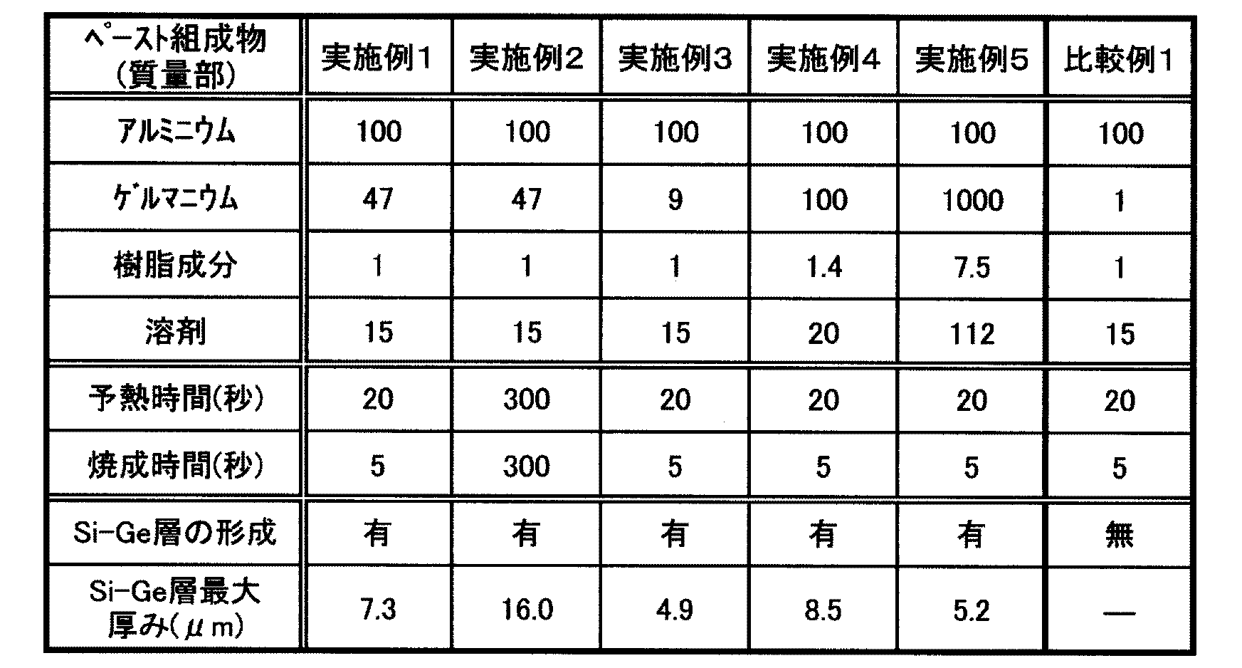
- a paste composition was prepared by adding 47 parts by weight of germanium powder, 1 part by weight of ethyl cellulose resin as a resin component, and 15 parts by weight of diethylene glycol monobutyl ether as a dispersion medium to 100 parts by weight of aluminum powder. .
- the prepared paste composition was applied onto a p-type silicon substrate at a coating amount of 7 mg / cm 2 so that the thickness was 180 ⁇ m.
- the organic matter is removed by preheating at a temperature of 400 ° C. for 20 seconds, followed by baking at a temperature of 860 ° C. for 5 seconds to form a p-type silicon substrate.
- a silicon germanium layer (Si-Ge layer), an aluminum-silicon germanium layer (Al-Si-Ge layer), and an aluminum germanium sintered body layer (Al-Ge sintered body layer) are formed on the top and the bottom in order. As a result, a laminated body was obtained.
- Al—Si—Ge layer aluminum-silicon germanium layer
- Al—Ge sintered body layer aluminum germanium sintered body layer
- Example 2 A laminated body in which a silicon germanium layer (Si—Ge layer) was formed on a p-type silicon substrate was manufactured in the same manner as in Example 1 except that the preheating time was 300 seconds and the heating time was 300 seconds. As in Example 1, by firing, a silicon germanium layer (Si—Ge layer), an aluminum-silicon germanium layer (Al—Si—Ge layer), and an aluminum germanium sintered body layer (in order from the bottom) on a p-type silicon substrate ( It was confirmed that an Al—Ge sintered body layer) was formed. Although the thickness of the silicon germanium layer varies depending on the measurement location, the maximum thickness was 16.0 ⁇ m.
- Example 3 A paste composition was prepared in the same manner as in Example 1 except that the amount of germanium powder added was 9 parts by mass with respect to 100 parts by mass of the aluminum powder, and a silicon germanium layer (Si—Ge layer) was formed on the p-type silicon substrate. ) was produced. As in Example 1, by firing, a silicon germanium layer (Si—Ge layer), an aluminum-silicon germanium layer (Al—Si—Ge layer), and an aluminum germanium sintered body layer (in order from the bottom) on a p-type silicon substrate ( It was confirmed that an Al—Ge sintered body layer) was formed. Although the thickness of the silicon germanium layer varies depending on the measurement location, the maximum thickness was 4.9 ⁇ m.
- Example 4 The amount of germanium powder added was 100 parts by mass with respect to 100 parts by mass of aluminum powder, the amount of resin component added was 1.4 parts by mass, and the amount of solvent added was 20 parts by mass.
- a paste composition was prepared to produce a laminate in which a silicon germanium layer (Si—Ge layer) was formed on a p-type silicon substrate. By firing, it was confirmed that a silicon germanium layer (Si—Ge layer) and an aluminum germanium sintered body layer (Al—Ge sintered body layer) were formed on the p-type silicon substrate sequentially from the bottom. Although the thickness of the silicon germanium layer varies depending on the measurement location, the maximum thickness was 8.5 ⁇ m.
- the addition amount of germanium powder was 1000 parts by mass with respect to 100 parts by mass of the aluminum powder, the addition amount of the resin component was 7.5 parts by mass, and the addition amount of the solvent was 112 parts by mass.
- a paste composition was prepared to produce a laminate in which a silicon germanium layer (Si—Ge layer) was formed on a p-type silicon substrate. By firing, it was confirmed that a silicon germanium layer (Si—Ge layer) and an aluminum germanium sintered body layer (Al—Ge sintered body layer) were formed on the p-type silicon substrate sequentially from the bottom. Although the thickness of the silicon germanium layer varies depending on the measurement location, the maximum thickness was 5.2 ⁇ m.
- Example 1 A paste composition was prepared in the same manner as in Example 1 except that the amount of germanium powder added was 1 part by mass with respect to 100 parts by mass of the aluminum powder, and a laminate was produced. By firing, it was confirmed that only an aluminum germanium sintered body layer (Al—Ge sintered body layer) was formed on the p-type silicon substrate, and formation of a silicon germanium layer was not confirmed.
- Al—Ge sintered body layer Al—Ge sintered body layer
- the thickness of the silicon germanium layer can be controlled by changing the germanium content and the firing time with respect to 100 parts by mass of aluminum in the paste composition.
- the thickness of the silicon germanium layer required varies depending on the application. For example, a transistor having a thickness of 10 to 100 nm is required for an IC application transistor, and a thickness of 1 to 100 ⁇ m for a single transistor element. According to the method, it has been found that a silicon germanium layer having a required thickness can be formed.
- a silicon germanium layer can be formed by applying the paste composition of the present invention and baking it for a short baking time of 10 to 300 seconds.
- batch processing in a vacuum apparatus is performed in the prior art, but according to the method for forming a silicon germanium layer of the present invention, continuous processing of a printing process and a baking process is possible, and the production efficiency is excellent. I understood.
- the surface was polished, the aluminum germanium sintered body layer was removed, and a measurement laminate in which a silicon germanium layer was formed on a p-type silicon substrate was produced.
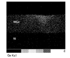
- FIG. 3 shows an SEM observation image of a cross section of the measurement sample
- FIG. 4 shows an element detection image by EDS.
- XRD measurement X-ray diffraction (XRD) measurement was performed on the surface of the measurement laminate using an X-ray diffractometer (product name: SmartLab, manufactured by Rigaku Corporation), and the plane orientation of the formed silicon germanium layer was measured.
- FIG. 5 shows the XRD measurement results.
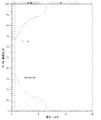
- the concentration of germanium in the silicon germanium layer of the measurement laminate is measured by secondary ion mass spectrometry (SIMS) using a secondary ion mass spectrometer (product name: IMS-7f, manufactured by Ametec Corporation, Kameka Division). did.
- the measurement was performed by setting the surface of the silicon germanium layer to 0 ⁇ m and measuring the impurity concentration in the depth direction. The results are shown in FIG.
- SYMBOLS 1 Silicon-containing substrate, 2 ... Silicon germanium layer (Si-Ge layer), 3 ... Aluminum-silicon germanium layer (Al-Si-Ge layer), 4 ... Aluminum germanium sintered body layer (Al-Ge sintered body layer) )
Landscapes
- Chemical & Material Sciences (AREA)
- Engineering & Computer Science (AREA)
- Wood Science & Technology (AREA)
- Life Sciences & Earth Sciences (AREA)
- Physics & Mathematics (AREA)
- Spectroscopy & Molecular Physics (AREA)
- Dispersion Chemistry (AREA)
- Inorganic Chemistry (AREA)
- Organic Chemistry (AREA)
- Materials Engineering (AREA)
- Photovoltaic Devices (AREA)
- Manufacturing & Machinery (AREA)
- Silicon Compounds (AREA)
- Laminated Bodies (AREA)
- Liquid Deposition Of Substances Of Which Semiconductor Devices Are Composed (AREA)
- Recrystallisation Techniques (AREA)
Abstract
Description
アルミニウム及びゲルマニウムを含み、ゲルマニウムの含有量がアルミニウムに対して特定の範囲の含有量であるペースト組成物が上記目的を達成できることを見出し、本発明を完成するに至った。
1.シリコンゲルマニウム層を形成するためのペースト組成物であって、
アルミニウム及びゲルマニウムを含み、前記ゲルマニウムの含有量は、前記アルミニウム100質量部に対して1質量部を超え、10000質量部以下である、ことを特徴とするペースト組成物。
2.更に、樹脂成分を含む、項1に記載のペースト組成物。
3.前記樹脂成分の含有量は、前記アルミニウム100質量部に対して0.1~10質量部である、項2に記載のペースト組成物。
4.更に、ガラス成分を含む、項1~3のいずれかに記載のペースト組成物。
5.前記ガラス成分の含有量は、前記アルミニウム100質量部に対して0.01~3質量部である、項4に記載のペースト組成物。
6.シリコンゲルマニウム層の形成方法であって、
(1)ケイ素含有基板上に、アルミニウム及びゲルマニウムを含み、前記ゲルマニウムの含有量が、前記アルミニウム100質量部に対して1質量部を超え、10000質量部以下であるペースト組成物を塗布する工程1、及び
(2)前記ペースト組成物が塗布された基板を焼成する工程2
を有する、ことを特徴とする形成方法。
7.前記焼成は、500~1000℃の温度で行われる、項6に記載の形成方法。
本発明のペースト組成物は、シリコンゲルマニウム層を形成するためのペースト組成物であって、アルミニウム及びゲルマニウムを含み、上記ゲルマニウムの含有量は、上記アルミニウム100質量部に対して1質量部を超え、10000質量部以下である。
アルミニウムとしては、ペースト組成物中に含まれ得る形態であれば特に限定されず、例えば、アルミニウム粉末が挙げられる。
ゲルマニウムとしては、ペースト組成物中に含まれ得る形態であれば特に限定されず、例えば、ゲルマニウム粉末が挙げられる。
本発明のペースト組成物は、ガラス成分を含有していてもよい。ペースト組成物がガラス粉末を含有することにより、アルミニウムとケイ素との反応性がより優れ、これにより、ゲルマニウムのケイ素との反応性が向上して、より容易にシリコンゲルマニウム層を形成することができる。
本発明のペースト組成物は、樹脂成分を含有していてもよい。ペースト組成物が樹脂成分を含有することにより、ペースト組成物の安定性及び印刷性を向上させることができる。
本発明のペースト組成物は、分散媒を含有していてもよい。ペースト組成物が分散媒を含有することにより、ペースト組成物の印刷性を向上させることができる。
本発明のペースト組成物は、上記アルミニウム、ゲルマニウム、ガラス成分、樹脂成分及び分散媒の他に、その他の添加剤を含有していてもよい。このような添加剤としては本発明の効果を妨げなければ特に限定されず、例えば、酸化防止剤、腐食抑制剤、消泡剤、増粘剤(タックファイヤー)、カップリング剤、静電付与剤、重合禁止剤、チキソトロピー剤、沈降防止剤等が挙げられる。具体的には、例えば、ポリエチレングリコールエステル化合物、ポリオキシエチレンソルビタンエステル化合物、ソルビタンアルキルエステル化合物、脂肪族多価カルボン酸化合物、燐酸エステル化合物、ポリエステル酸のアマイドアミン塩、酸化ポリエチレン系化合物、脂肪酸アマイドワックス等を使用することができる。
本発明のシリコンゲルマニウム層の形成方法は、下記工程1及び2を有する形成方法である。
(1)ケイ素含有基板上に、アルミニウム及びゲルマニウムを含み、上記ゲルマニウムの含有量が、上記アルミニウム100質量部に対して1質量部を超え、10000質量部以下であるペースト組成物を塗布する工程1、及び
(2)上記ペースト組成物が塗布されたケイ素含有基板を焼成する工程2
を有する、ことを特徴とする形成方法。
以下、詳細に説明する。
工程1は、ケイ素含有基板上に、アルミニウム及びゲルマニウムを含み、上記ゲルマニウムの含有量が、上記アルミニウム100質量部に対して1質量部を超え、10000質量部以下であるペースト組成物を塗布する工程である。
工程2は、上記ペースト組成物が塗布されたケイ素含有基板を焼成する工程である。
本発明のシリコンゲルマニウム層の形成方法は、上記工程1と、工程2との間に、ケイ素含有基板上に塗布された上記ペースト組成物から樹脂成分等を除去するための予熱工程を有していてもよい。予熱工程を有することにより、ペースト組成物中に存在する樹脂成分を除去することができ、同時に分散媒も除去することができるので、シリコンゲルマニウム層をより十分に形成することができる。
本発明のシリコンゲルマニウム層の形成方法は、上記予熱工程の前に、ケイ素含有基板上に塗布された上記ペースト組成物を乾燥させる乾燥工程を有していてもよい。乾燥工程を有することにより、ペースト組成物中に存在する分散媒を予めある程度除去することができ、シリコンゲルマニウム層をより十分に形成することができる。
本発明のシリコンゲルマニウム層の形成方法は、上記工程2の後に、工程2でシリコンゲルマニウム層上に形成された、上記アルミニウム-シリコンゲルマニウム層(Al-Si-Ge層)やアルミニウムゲルマニウム焼結体層(Al-Ge焼結体層)等の不要な層を除去する工程を有していてもよい。
以下の原料を用意した。
・アルミニウム粉末:東洋アルミニウム(株)製;アルミニウム含有量99.9質量%の球状粉末 平均粒子径4μm
・ゲルマニウム粉末:Ge Powder(フルウチ化学(株)製;ゲルマニウム含有量99.999質量%の非球状粉末 平均粒子径10μm)
・樹脂成分:エチルセルロース樹脂(Dow(株)製)
予熱時間を300秒間とし、加熱時間を300秒間として焼成した以外は実施例1と同様にして、p型シリコン基板上にシリコンゲルマニウム層(Si-Ge層)が形成された積層体を製造した。
実施例1と同様に、焼成により、p型シリコン基板上に下から順にシリコンゲルマニウム層(Si-Ge層)、アルミニウム-シリコンゲルマニウム層(Al-Si-Ge層)及びアルミニウムゲルマニウム焼結体層(Al-Ge焼結体層)が形成されていることが確認された。シリコンゲルマニウム層の厚みは、測定箇所によりばらつきが見られるが、最大厚みは16.0μmであった。
ゲルマニウム粉末の添加量を、アルミニウム粉末100質量部に対して9質量部とした以外は実施例1と同様にしてペースト組成物を調製し、p型シリコン基板上にシリコンゲルマニウム層(Si-Ge層)が形成された積層体を製造した。
実施例1と同様に、焼成により、p型シリコン基板上に下から順にシリコンゲルマニウム層(Si-Ge層)、アルミニウム-シリコンゲルマニウム層(Al-Si-Ge層)及びアルミニウムゲルマニウム焼結体層(Al-Ge焼結体層)が形成されていることが確認された。シリコンゲルマニウム層の厚みは、測定箇所によりばらつきが見られるが、最大厚みは4.9μmであった。
ゲルマニウム粉末の添加量を、アルミニウム粉末100質量部に対して100質量部とし、樹脂成分の添加量を1.4質量部、溶剤の添加量を20質量部とした以外は実施例1と同様にしてペースト組成物を調製し、p型シリコン基板上にシリコンゲルマニウム層(Si-Ge層)が形成された積層体を製造した。
焼成により、p型シリコン基板上に、下から順にシリコンゲルマニウム層(Si-Ge層)及びアルミニウムゲルマニウム焼結体層(Al-Ge焼結体層)が形成されていることが確認された。シリコンゲルマニウム層の厚みは、測定箇所によりばらつきが見られるが、最大厚みは8.5μmであった。
ゲルマニウム粉末の添加量を、アルミニウム粉末100質量部に対して1000質量部とし、樹脂成分の添加量を7.5質量部、溶剤の添加量を112質量部とした以外は実施例1と同様にしてペースト組成物を調製し、p型シリコン基板上にシリコンゲルマニウム層(Si-Ge層)が形成された積層体を製造した。
焼成により、p型シリコン基板上に、下から順にシリコンゲルマニウム層(Si-Ge層)及びアルミニウムゲルマニウム焼結体層(Al-Ge焼結体層)が形成されていることが確認された。シリコンゲルマニウム層の厚みは、測定箇所によりばらつきが見られるが、最大厚みは5.2μmであった。
ゲルマニウム粉末の添加量を、アルミニウム粉末100質量部に対して1質量部とした以外は実施例1と同様にしてペースト組成物を調製し、積層体を製造した。
焼成により、p型シリコン基板上にアルミニウムゲルマニウム焼結体層(Al-Ge焼結体層)のみが形成されていることが確認され、シリコンゲルマニウム層の形成は確認されなかった。
実施例4と同様にして、焼成によりp型シリコン基板上に、下から順にシリコンゲルマニウム層(Si-Ge層)及びアルミニウムゲルマニウム焼結体層(Al-Ge焼結体層)を形成し、これらが積層された積層体を得た。
上記測定用積層体を、イオンミリングにより測定用積層体表面に垂直方向に切断した測定用試料を作製した。測定用試料の断面に対し、走査型電子顕微鏡(SEM)及びエネルギー分散型X線分析(EDS)(日本電子社製、型番:JSM-6510)を用いて、観察及び元素マッピングを行なった。図3に測定用試料の断面のSEM観察画像を示し、図4にEDSによる元素検出画像を示す。
上記測定用積層体の表面に、X線回折装置(リガク社製 製品名:SmartLab)を用いてX線回折(XRD)測定を実施し、形成されたシリコンゲルマニウム層の面方位を測定した。図5にXRD測定結果を示す。
上記測定用積層体のシリコンゲルマニウム層中のゲルマニウム濃度を、二次イオン質量分析装置(アメテック株式会社 カメカ事業部製 製品名:IMS‐7f)を用いて二次イオン質量測定法(SIMS)により測定した。測定は、シリコンゲルマニウム層の表面を0μmとして、深さ方向に対する不純物濃度を測定することにより行った。結果を図6に示す。
Claims (7)
- シリコンゲルマニウム層を形成するためのペースト組成物であって、
アルミニウム及びゲルマニウムを含み、前記ゲルマニウムの含有量は、前記アルミニウム100質量部に対して1質量部を超え、10000質量部以下である、ことを特徴とするペースト組成物。 - 更に、樹脂成分を含む、請求項1に記載のペースト組成物。
- 前記樹脂成分の含有量は、前記アルミニウム100質量部に対して0.1~10質量部である、請求項2に記載のペースト組成物。
- 更に、ガラス成分を含む、請求項1~3のいずれかに記載のペースト組成物。
- 前記ガラス成分の含有量は、前記アルミニウム100質量部に対して0.01~3質量部である、請求項4に記載のペースト組成物。
- シリコンゲルマニウム層の形成方法であって、
(1)ケイ素含有基板上に、アルミニウム及びゲルマニウムを含み、前記ゲルマニウムの含有量が、前記アルミニウム100質量部に対して1質量部を超え、10000質量部以下であるペースト組成物を塗布する工程1、及び
(2)前記ペースト組成物が塗布されたケイ素含有基板を焼成する工程2
を有する、ことを特徴とする形成方法。 - 前記焼成は、500~1000℃の温度で行われる、請求項6に記載の形成方法。
Priority Applications (5)
| Application Number | Priority Date | Filing Date | Title |
|---|---|---|---|
| KR1020187010912A KR102685852B1 (ko) | 2015-09-24 | 2016-09-16 | 페이스트 조성물 및 실리콘 게르마늄 층의 형성 방법 |
| EP16848563.9A EP3355340B1 (en) | 2015-09-24 | 2016-09-16 | Use of paste composition and method for forming silicon germanium layer |
| US15/762,321 US10916423B2 (en) | 2015-09-24 | 2016-09-16 | Paste composition and method for forming silicon germanium layer |
| CN201680055095.4A CN108028187B (zh) | 2015-09-24 | 2016-09-16 | 膏状组合物及硅锗层的形成方法 |
| JP2017541539A JP6766054B2 (ja) | 2015-09-24 | 2016-09-16 | ペースト組成物及びシリコンゲルマニウム層の形成方法 |
Applications Claiming Priority (2)
| Application Number | Priority Date | Filing Date | Title |
|---|---|---|---|
| JP2015187017 | 2015-09-24 | ||
| JP2015-187017 | 2015-09-24 |
Publications (1)
| Publication Number | Publication Date |
|---|---|
| WO2017051775A1 true WO2017051775A1 (ja) | 2017-03-30 |
Family
ID=58386442
Family Applications (1)
| Application Number | Title | Priority Date | Filing Date |
|---|---|---|---|
| PCT/JP2016/077439 Ceased WO2017051775A1 (ja) | 2015-09-24 | 2016-09-16 | ペースト組成物及びシリコンゲルマニウム層の形成方法 |
Country Status (7)
| Country | Link |
|---|---|
| US (1) | US10916423B2 (ja) |
| EP (1) | EP3355340B1 (ja) |
| JP (1) | JP6766054B2 (ja) |
| KR (1) | KR102685852B1 (ja) |
| CN (1) | CN108028187B (ja) |
| TW (1) | TWI616938B (ja) |
| WO (1) | WO2017051775A1 (ja) |
Cited By (2)
| Publication number | Priority date | Publication date | Assignee | Title |
|---|---|---|---|---|
| WO2022209228A1 (ja) * | 2021-03-31 | 2022-10-06 | 東洋アルミニウム株式会社 | ペースト組成物、及び、ゲルマニウム化合物層の形成方法 |
| WO2025239235A1 (ja) * | 2024-05-13 | 2025-11-20 | 東洋アルミニウム株式会社 | n型シリコンゲルマニウム層の形成方法 |
Families Citing this family (1)
| Publication number | Priority date | Publication date | Assignee | Title |
|---|---|---|---|---|
| EP3605587A4 (en) * | 2017-03-27 | 2020-12-30 | Kanto Denka Kogyo Co., Ltd. | DRY ENGRAVING OR DRY CLEANING PROCESS |
Citations (5)
| Publication number | Priority date | Publication date | Assignee | Title |
|---|---|---|---|---|
| JPH05298917A (ja) * | 1992-04-20 | 1993-11-12 | Okuno Chem Ind Co Ltd | 導電性アルミニウムペースト用組成物 |
| JPH09172204A (ja) * | 1995-12-19 | 1997-06-30 | Ngk Insulators Ltd | 熱電変換装置およびその製造方法 |
| US20150090325A1 (en) * | 2013-09-27 | 2015-04-02 | Richard Hamilton SEWELL | Metal Seed Layer for Solar Cell Conductive Contact |
| JP2015122506A (ja) * | 2008-08-07 | 2015-07-02 | 京都エレックス株式会社 | 太陽電池素子の電極形成用導電性ペースト及び太陽電池素子並びにその太陽電池素子の製造方法 |
| JP2015153567A (ja) * | 2014-02-13 | 2015-08-24 | 大研化学工業株式会社 | 電極ペースト、電極形成方法及び電極構造 |
Family Cites Families (20)
| Publication number | Priority date | Publication date | Assignee | Title |
|---|---|---|---|---|
| US6855436B2 (en) * | 2003-05-30 | 2005-02-15 | International Business Machines Corporation | Formation of silicon-germanium-on-insulator (SGOI) by an integral high temperature SIMOX-Ge interdiffusion anneal |
| JP4213408B2 (ja) | 2002-06-17 | 2009-01-21 | 日鉱金属株式会社 | 高純度Si−Ge合金ターゲット及びその製造方法 |
| JP3851950B2 (ja) | 2002-11-19 | 2006-11-29 | 国立大学法人名古屋大学 | シリコンゲルマニウム膜の作製方法、エピタキシャル成長用基板、多層膜構造体及びヘテロ接合電界効果トランジスタ |
| JP2008506617A (ja) * | 2004-07-15 | 2008-03-06 | アイクストロン、アーゲー | SiとGeを含有する膜の堆積方法 |
| US7678420B2 (en) * | 2005-06-22 | 2010-03-16 | Sandisk 3D Llc | Method of depositing germanium films |
| US7892872B2 (en) * | 2007-01-03 | 2011-02-22 | Nanogram Corporation | Silicon/germanium oxide particle inks, inkjet printing and processes for doping semiconductor substrates |
| JP2009129600A (ja) * | 2007-11-21 | 2009-06-11 | Toyo Aluminium Kk | ペースト組成物と太陽電池素子 |
| US8043532B2 (en) * | 2007-11-22 | 2011-10-25 | Cheil Industries Inc. | Composition for electrodes comprising aluminum powder having controlled particle size distribution and size, and electrodes made using the same |
| US8231934B2 (en) * | 2008-11-26 | 2012-07-31 | E. I. Du Pont De Nemours And Company | Conductive paste for solar cell electrode |
| CN102341866A (zh) * | 2009-03-06 | 2012-02-01 | 东洋铝株式会社 | 导电糊组合物和使用该导电糊组合物形成的导电膜 |
| JP2011035024A (ja) * | 2009-07-30 | 2011-02-17 | Toyo Aluminium Kk | ペースト組成物およびそれを用いた太陽電池素子 |
| EP2315239A1 (en) | 2009-10-23 | 2011-04-27 | Imec | A method of forming monocrystalline germanium or silicon germanium |
| US8895962B2 (en) * | 2010-06-29 | 2014-11-25 | Nanogram Corporation | Silicon/germanium nanoparticle inks, laser pyrolysis reactors for the synthesis of nanoparticles and associated methods |
| US20120152342A1 (en) * | 2010-12-16 | 2012-06-21 | E.I. Du Pont De Nemours And Company | Aluminum paste compositions comprising metal phosphates and their use in manufacturing solar cells |
| US8815636B2 (en) * | 2011-01-06 | 2014-08-26 | Heraeus Precious Metals North America Conshohocken Llc | Oxides and glasses for use with aluminum back solar cell contacts |
| JP5673316B2 (ja) * | 2011-04-11 | 2015-02-18 | 日立化成株式会社 | 電子部品、それに適用されるアルミニウム電極用導電性ペースト、及びアルミニウム電極用ガラス組成物 |
| JP5494619B2 (ja) * | 2011-11-09 | 2014-05-21 | 日立化成株式会社 | 電子部品、それに適用されるアルミニウム電極用導電性ペースト、及びアルミニウム電極用ガラス組成物 |
| WO2013115076A1 (ja) | 2012-02-02 | 2013-08-08 | 東洋アルミニウム株式会社 | ペースト組成物 |
| TWI577742B (zh) * | 2014-06-20 | 2017-04-11 | 賀利氏貴金屬北美康舍霍肯有限責任公司 | 用於導電性漿料之有機載體 |
| JP6195597B2 (ja) * | 2015-09-29 | 2017-09-13 | 東洋アルミニウム株式会社 | ペースト組成物 |
-
2016
- 2016-09-16 JP JP2017541539A patent/JP6766054B2/ja active Active
- 2016-09-16 CN CN201680055095.4A patent/CN108028187B/zh active Active
- 2016-09-16 EP EP16848563.9A patent/EP3355340B1/en active Active
- 2016-09-16 US US15/762,321 patent/US10916423B2/en active Active
- 2016-09-16 KR KR1020187010912A patent/KR102685852B1/ko active Active
- 2016-09-16 WO PCT/JP2016/077439 patent/WO2017051775A1/ja not_active Ceased
- 2016-09-19 TW TW105130174A patent/TWI616938B/zh active
Patent Citations (5)
| Publication number | Priority date | Publication date | Assignee | Title |
|---|---|---|---|---|
| JPH05298917A (ja) * | 1992-04-20 | 1993-11-12 | Okuno Chem Ind Co Ltd | 導電性アルミニウムペースト用組成物 |
| JPH09172204A (ja) * | 1995-12-19 | 1997-06-30 | Ngk Insulators Ltd | 熱電変換装置およびその製造方法 |
| JP2015122506A (ja) * | 2008-08-07 | 2015-07-02 | 京都エレックス株式会社 | 太陽電池素子の電極形成用導電性ペースト及び太陽電池素子並びにその太陽電池素子の製造方法 |
| US20150090325A1 (en) * | 2013-09-27 | 2015-04-02 | Richard Hamilton SEWELL | Metal Seed Layer for Solar Cell Conductive Contact |
| JP2015153567A (ja) * | 2014-02-13 | 2015-08-24 | 大研化学工業株式会社 | 電極ペースト、電極形成方法及び電極構造 |
Non-Patent Citations (1)
| Title |
|---|
| See also references of EP3355340A4 * |
Cited By (4)
| Publication number | Priority date | Publication date | Assignee | Title |
|---|---|---|---|---|
| WO2022209228A1 (ja) * | 2021-03-31 | 2022-10-06 | 東洋アルミニウム株式会社 | ペースト組成物、及び、ゲルマニウム化合物層の形成方法 |
| JP2022157011A (ja) * | 2021-03-31 | 2022-10-14 | 東洋アルミニウム株式会社 | ペースト組成物、及び、ゲルマニウム化合物層の形成方法 |
| JP7680867B2 (ja) | 2021-03-31 | 2025-05-21 | 東洋アルミニウム株式会社 | ペースト組成物、及び、ゲルマニウム化合物層の形成方法 |
| WO2025239235A1 (ja) * | 2024-05-13 | 2025-11-20 | 東洋アルミニウム株式会社 | n型シリコンゲルマニウム層の形成方法 |
Also Published As
| Publication number | Publication date |
|---|---|
| JP6766054B2 (ja) | 2020-10-07 |
| US20180301334A1 (en) | 2018-10-18 |
| TWI616938B (zh) | 2018-03-01 |
| TW201715581A (zh) | 2017-05-01 |
| JPWO2017051775A1 (ja) | 2018-07-12 |
| CN108028187B (zh) | 2022-06-07 |
| EP3355340A1 (en) | 2018-08-01 |
| KR102685852B1 (ko) | 2024-07-16 |
| CN108028187A (zh) | 2018-05-11 |
| EP3355340B1 (en) | 2020-09-09 |
| US10916423B2 (en) | 2021-02-09 |
| KR20180059474A (ko) | 2018-06-04 |
| EP3355340A4 (en) | 2019-05-22 |
Similar Documents
| Publication | Publication Date | Title |
|---|---|---|
| KR101788240B1 (ko) | 구리 셀레나이드 나노 입자의 제조 | |
| JP6688832B2 (ja) | アンチモンがドープされたナノ粒子 | |
| JP6766054B2 (ja) | ペースト組成物及びシリコンゲルマニウム層の形成方法 | |
| JP2013071864A (ja) | 離型剤用窒化ケイ素粉末およびその製造方法 | |
| US20240158903A1 (en) | Paste composition, and method for forming germanium compound layer | |
| Mokurala et al. | Low temperature synthesis and characterization of Cu2ZnSnS4 (CZTS) nanoparticle by solution based solid state reaction method | |
| KR101442559B1 (ko) | 코팅액 조성물 및 이를 이용한 고품질 세라믹 코팅층의 형성방법 | |
| JP2009215502A (ja) | 脂環式・芳香族炭化水素を溶媒とする銀インク | |
| WO2025239235A1 (ja) | n型シリコンゲルマニウム層の形成方法 | |
| JP6938333B2 (ja) | シリコン混晶層の製造方法 | |
| DE102005056446A1 (de) | Siliciumpulver enthaltende Dispersion und Verfahren zur Beschichtung | |
| TW201526277A (zh) | 二硒化/二硫化富銅的銅銦(鎵)奈米粒子的製備 | |
| JPWO2013180137A1 (ja) | 化合物半導体薄膜の作製方法およびその化合物半導体薄膜を備える太陽電池 | |
| KR101431457B1 (ko) | 도가니 보호막 제조 방법 | |
| WO2013154374A1 (en) | Fabrication method of photo active layer for solar cell | |
| KR101395790B1 (ko) | 태양전지 광활성층의 제조방법 | |
| JP2009215503A (ja) | 非極性炭化水素を溶媒とする分散性に優れた銀インク | |
| KR101395779B1 (ko) | 태양전지 광활성층의 제조방법 | |
| TWI485872B (zh) | 漿料與太陽能電池之吸光層的形成方法 | |
| Petrović et al. | Methodologies Used for the Synthesis of Cuprous Oxide as an Active Solar Cell Material | |
| WO2018211900A1 (ja) | 酸化物焼結体およびスパッタリングターゲット |
Legal Events
| Date | Code | Title | Description |
|---|---|---|---|
| 121 | Ep: the epo has been informed by wipo that ep was designated in this application |
Ref document number: 16848563 Country of ref document: EP Kind code of ref document: A1 |
|
| ENP | Entry into the national phase |
Ref document number: 2017541539 Country of ref document: JP Kind code of ref document: A |
|
| WWE | Wipo information: entry into national phase |
Ref document number: 15762321 Country of ref document: US |
|
| NENP | Non-entry into the national phase |
Ref country code: DE |
|
| ENP | Entry into the national phase |
Ref document number: 20187010912 Country of ref document: KR Kind code of ref document: A |
|
| WWE | Wipo information: entry into national phase |
Ref document number: 2016848563 Country of ref document: EP |