WO2017047284A1 - 半導体装置および半導体装置の製造方法 - Google Patents
半導体装置および半導体装置の製造方法 Download PDFInfo
- Publication number
- WO2017047284A1 WO2017047284A1 PCT/JP2016/073367 JP2016073367W WO2017047284A1 WO 2017047284 A1 WO2017047284 A1 WO 2017047284A1 JP 2016073367 W JP2016073367 W JP 2016073367W WO 2017047284 A1 WO2017047284 A1 WO 2017047284A1
- Authority
- WO
- WIPO (PCT)
- Prior art keywords
- film
- conductivity type
- band gap
- insulating film
- semiconductor
- Prior art date
- Legal status (The legal status is an assumption and is not a legal conclusion. Google has not performed a legal analysis and makes no representation as to the accuracy of the status listed.)
- Ceased
Links
Images



Classifications
-
- H—ELECTRICITY
- H10—SEMICONDUCTOR DEVICES; ELECTRIC SOLID-STATE DEVICES NOT OTHERWISE PROVIDED FOR
- H10D—INORGANIC ELECTRIC SEMICONDUCTOR DEVICES
- H10D64/00—Electrodes of devices having potential barriers
- H10D64/118—Electrodes comprising insulating layers having particular dielectric or electrostatic properties, e.g. having static charges
-
- H—ELECTRICITY
- H10—SEMICONDUCTOR DEVICES; ELECTRIC SOLID-STATE DEVICES NOT OTHERWISE PROVIDED FOR
- H10D—INORGANIC ELECTRIC SEMICONDUCTOR DEVICES
- H10D12/00—Bipolar devices controlled by the field effect, e.g. insulated-gate bipolar transistors [IGBT]
- H10D12/01—Manufacture or treatment
- H10D12/031—Manufacture or treatment of IGBTs
-
- H—ELECTRICITY
- H10—SEMICONDUCTOR DEVICES; ELECTRIC SOLID-STATE DEVICES NOT OTHERWISE PROVIDED FOR
- H10D—INORGANIC ELECTRIC SEMICONDUCTOR DEVICES
- H10D30/00—Field-effect transistors [FET]
- H10D30/60—Insulated-gate field-effect transistors [IGFET]
- H10D30/64—Double-diffused metal-oxide semiconductor [DMOS] FETs
- H10D30/66—Vertical DMOS [VDMOS] FETs
-
- H—ELECTRICITY
- H10—SEMICONDUCTOR DEVICES; ELECTRIC SOLID-STATE DEVICES NOT OTHERWISE PROVIDED FOR
- H10D—INORGANIC ELECTRIC SEMICONDUCTOR DEVICES
- H10D30/00—Field-effect transistors [FET]
- H10D30/60—Insulated-gate field-effect transistors [IGFET]
- H10D30/64—Double-diffused metal-oxide semiconductor [DMOS] FETs
- H10D30/66—Vertical DMOS [VDMOS] FETs
- H10D30/665—Vertical DMOS [VDMOS] FETs having edge termination structures
-
- H—ELECTRICITY
- H10—SEMICONDUCTOR DEVICES; ELECTRIC SOLID-STATE DEVICES NOT OTHERWISE PROVIDED FOR
- H10D—INORGANIC ELECTRIC SEMICONDUCTOR DEVICES
- H10D62/00—Semiconductor bodies, or regions thereof, of devices having potential barriers
- H10D62/10—Shapes, relative sizes or dispositions of the regions of the semiconductor bodies; Shapes of the semiconductor bodies
- H10D62/17—Semiconductor regions connected to electrodes not carrying current to be rectified, amplified or switched, e.g. channel regions
- H10D62/393—Body regions of DMOS transistors or IGBTs
-
- H—ELECTRICITY
- H10—SEMICONDUCTOR DEVICES; ELECTRIC SOLID-STATE DEVICES NOT OTHERWISE PROVIDED FOR
- H10D—INORGANIC ELECTRIC SEMICONDUCTOR DEVICES
- H10D62/00—Semiconductor bodies, or regions thereof, of devices having potential barriers
- H10D62/80—Semiconductor bodies, or regions thereof, of devices having potential barriers characterised by the materials
- H10D62/81—Semiconductor bodies, or regions thereof, of devices having potential barriers characterised by the materials of structures exhibiting quantum-confinement effects, e.g. single quantum wells; of structures having periodic or quasi-periodic potential variation
-
- H—ELECTRICITY
- H10—SEMICONDUCTOR DEVICES; ELECTRIC SOLID-STATE DEVICES NOT OTHERWISE PROVIDED FOR
- H10D—INORGANIC ELECTRIC SEMICONDUCTOR DEVICES
- H10D62/00—Semiconductor bodies, or regions thereof, of devices having potential barriers
- H10D62/80—Semiconductor bodies, or regions thereof, of devices having potential barriers characterised by the materials
- H10D62/83—Semiconductor bodies, or regions thereof, of devices having potential barriers characterised by the materials being Group IV materials, e.g. B-doped Si or undoped Ge
- H10D62/832—Semiconductor bodies, or regions thereof, of devices having potential barriers characterised by the materials being Group IV materials, e.g. B-doped Si or undoped Ge being Group IV materials comprising two or more elements, e.g. SiGe
- H10D62/8325—Silicon carbide
-
- H—ELECTRICITY
- H10—SEMICONDUCTOR DEVICES; ELECTRIC SOLID-STATE DEVICES NOT OTHERWISE PROVIDED FOR
- H10D—INORGANIC ELECTRIC SEMICONDUCTOR DEVICES
- H10D64/00—Electrodes of devices having potential barriers
- H10D64/01—Manufacture or treatment
- H10D64/011—Manufacture or treatment of electrodes ohmically coupled to a semiconductor
- H10D64/0111—Manufacture or treatment of electrodes ohmically coupled to a semiconductor to Group IV semiconductors
- H10D64/0115—Manufacture or treatment of electrodes ohmically coupled to a semiconductor to Group IV semiconductors to silicon carbide
-
- H—ELECTRICITY
- H10—SEMICONDUCTOR DEVICES; ELECTRIC SOLID-STATE DEVICES NOT OTHERWISE PROVIDED FOR
- H10D—INORGANIC ELECTRIC SEMICONDUCTOR DEVICES
- H10D64/00—Electrodes of devices having potential barriers
- H10D64/20—Electrodes characterised by their shapes, relative sizes or dispositions
- H10D64/23—Electrodes carrying the current to be rectified, amplified, oscillated or switched, e.g. sources, drains, anodes or cathodes
- H10D64/251—Source or drain electrodes for field-effect devices
- H10D64/252—Source or drain electrodes for field-effect devices for vertical or pseudo-vertical devices
-
- H—ELECTRICITY
- H10—SEMICONDUCTOR DEVICES; ELECTRIC SOLID-STATE DEVICES NOT OTHERWISE PROVIDED FOR
- H10P—GENERIC PROCESSES OR APPARATUS FOR THE MANUFACTURE OR TREATMENT OF DEVICES COVERED BY CLASS H10
- H10P30/00—Ion implantation into wafers, substrates or parts of devices
- H10P30/20—Ion implantation into wafers, substrates or parts of devices into semiconductor materials, e.g. for doping
- H10P30/22—Ion implantation into wafers, substrates or parts of devices into semiconductor materials, e.g. for doping using masks
-
- H—ELECTRICITY
- H10—SEMICONDUCTOR DEVICES; ELECTRIC SOLID-STATE DEVICES NOT OTHERWISE PROVIDED FOR
- H10W—GENERIC PACKAGES, INTERCONNECTIONS, CONNECTORS OR OTHER CONSTRUCTIONAL DETAILS OF DEVICES COVERED BY CLASS H10
- H10W72/00—Interconnections or connectors in packages
-
- H—ELECTRICITY
- H10—SEMICONDUCTOR DEVICES; ELECTRIC SOLID-STATE DEVICES NOT OTHERWISE PROVIDED FOR
- H10D—INORGANIC ELECTRIC SEMICONDUCTOR DEVICES
- H10D12/00—Bipolar devices controlled by the field effect, e.g. insulated-gate bipolar transistors [IGBT]
- H10D12/411—Insulated-gate bipolar transistors [IGBT]
- H10D12/441—Vertical IGBTs
-
- H—ELECTRICITY
- H10—SEMICONDUCTOR DEVICES; ELECTRIC SOLID-STATE DEVICES NOT OTHERWISE PROVIDED FOR
- H10D—INORGANIC ELECTRIC SEMICONDUCTOR DEVICES
- H10D64/00—Electrodes of devices having potential barriers
- H10D64/20—Electrodes characterised by their shapes, relative sizes or dispositions
- H10D64/23—Electrodes carrying the current to be rectified, amplified, oscillated or switched, e.g. sources, drains, anodes or cathodes
Definitions
- the present invention relates to a semiconductor device and a method for manufacturing the semiconductor device.
- silicon has been used as a constituent material of power semiconductor devices that control high voltage and large current.
- power semiconductor devices such as bipolar transistors, IGBTs (Insulated Gate Bipolar Transistors), MOSFETs (Metal Oxide Semiconductor Field Transistors, Insulated Gate Field Effect Transistors). It has been.
- bipolar transistors and IGBTs have a higher current density than MOSFETs and can be increased in current, but cannot be switched at high speed.
- the bipolar transistor is limited in use at a switching frequency of about several kHz
- the IGBT is limited in use at a switching frequency of about several tens of kHz.
- a power MOSFET has a lower current density than a bipolar transistor or IGBT and is difficult to increase in current, but can perform a high-speed switching operation up to several MHz.
- Silicon carbide is a chemically very stable semiconductor material, has a wide band gap of 3 eV, and can be used extremely stably as a semiconductor even at high temperatures. Silicon carbide is also expected as a semiconductor material that can sufficiently reduce the on-resistance because the maximum electric field strength is one digit or more larger than that of silicon. Such features of silicon carbide also apply to other wide band gap semiconductors having a wider band gap than silicon, for example, gallium nitride (GaN). For this reason, the use of a wide bandgap semiconductor can increase the breakdown voltage of the semiconductor device (for example, see Non-Patent Document 2 below).
- the carrier frequency is applied at a frequency one digit higher than that of a conventional semiconductor device using silicon.
- the heat generation temperature to the chip increases, which affects the reliability of the semiconductor device.
- a bonding wire is bonded to the front surface electrode, which is an electrode exposed on the front surface of the semiconductor device, as a wiring material for extracting the potential of the front surface electrode to the outside. If it is used, the adhesion between the front electrode and the bonding wire is lowered, which affects the reliability of the semiconductor device.
- FIG. 4 is a cross-sectional view showing a configuration of a conventional silicon carbide semiconductor device.
- N type silicon carbide epitaxial layer 2 is deposited on the surface of n + type silicon carbide substrate 1, and a plurality of p + type regions 10 are provided on the surface of n type silicon carbide epitaxial layer 2.
- a p-type silicon carbide epitaxial layer 11 is provided on the surface of p + -type region 10.
- N type well region 12 is provided in p type silicon carbide epitaxial layer 11 on n type silicon carbide epitaxial layer 2 where p + type region 10 is not provided.
- n + type source region 4 and p ++ type contact region 5 are provided on the surface of p type silicon carbide epitaxial layer 11.
- a gate electrode 7 is provided on the surface of the p-type silicon carbide epitaxial layer 11 sandwiched between the n + -type source region 4 and the n-type well region 12 via a gate insulating film 6.
- a PSG (Phospho Silicate Glass) film 14 is selectively provided.
- Source electrodes 8 are provided on the surfaces of the n + -type source region 4 and the p ++ -type contact region 5.
- a protective film 15 is selectively provided on the source electrode 8, and a plating film 16 is provided in a portion where the protective film 15 is not provided.
- a second protective film 17 is provided so as to cover a portion where the plating film 16 and the protective film 15 are adjacent to each other.
- Solder 19 for connecting a pin-like electrode 18 connected to an external signal is provided on the plating film 16 portion.
- a drain electrode 9 is provided on the back side of n + -type silicon carbide substrate 1.
- the coverage (step coverage) of the interlayer insulating film 13 is poor and a step due to the unevenness of the lower layer is formed on the surface of the interlayer insulating film 13, so that when the pin-shaped electrode 18 is soldered to the source electrode 8
- the step of interlayer insulating film 13 refers to a silicon carbide semiconductor substrate that includes n + -type silicon carbide substrate 1 and n-type silicon carbide epitaxial layer 2 that is generated when interlayer insulating film 13 covers gate electrode 7. This is the height of the interlayer insulating film 13.
- the plating film 16, the protective film 15, and the source electrode 8 are formed near the end of the solder 19. Stress concentrates on the three points of contact with each other due to the difference in thermal expansion. As the stress concentrates in this way, the characteristics of the semiconductor device are deteriorated and the reliability is lowered. In the worst case, the interlayer insulating film 13 is broken, the gate electrode 7 and the source electrode 8 are short-circuited, and the semiconductor device becomes defective.
- the characteristics of the semiconductor device deteriorate due to the penetration of the pretreatment liquid when the plating film 16 is formed and the adverse effect of the gas, such as fluctuation of the threshold voltage, and the reliability is lowered.
- An object of the present invention is to provide a semiconductor device and a semiconductor device manufacturing method that improve the reliability of a semiconductor device in which pin-shaped electrodes are joined by solder.
- the semiconductor device includes a first conductivity type wide band gap semiconductor substrate, a first conductivity type wide band gap semiconductor deposition layer, a second conductivity type semiconductor region, a second conductivity type wide band gap semiconductor layer, A first conductivity type region, a second first conductivity type region, a gate electrode, a source electrode, an interlayer insulating film, a drain electrode, a plating film, and a pin-like electrode are provided.
- the first conductivity type wide band gap semiconductor substrate is made of a semiconductor having a wider band gap than silicon.
- the first conductivity type wide band gap semiconductor deposition layer is deposited on the front surface of the first conductivity type wide band gap semiconductor substrate, and has an impurity concentration lower than that of the first conductivity type wide band gap semiconductor substrate.
- the second conductivity type semiconductor region is selectively provided on a surface layer of the first conductivity type wide band gap semiconductor deposition layer opposite to the first conductivity type wide band gap semiconductor substrate side.
- the second conductivity type wide band gap semiconductor layer is provided on the surface of the first conductivity type wide band gap semiconductor deposition layer and the second conductivity type semiconductor region, and is made of a semiconductor having a wider band gap than silicon.
- the first first conductivity type region is selectively provided on the first conductivity type wide band gap semiconductor deposition layer in the second conductivity type wide band gap semiconductor layer.
- the second first conductivity type region is selectively provided in the second conductivity type wide band gap semiconductor layer.
- the gate electrode is provided on the second first conductivity type region and the first first conductivity type region via a gate insulating film.
- the source electrode is in contact with the second conductivity type wide band gap semiconductor layer and the second first conductivity type region.
- the interlayer insulating film covers the gate electrode.
- the drain electrode is provided on the back surface of the first conductivity type wide band gap semiconductor substrate.
- the plating film is selectively provided on the source electrode.
- the pin-like electrode is connected to the plating film via solder and takes out an external signal.
- the interlayer insulating film has a structure in which a first insulating film and a second insulating film are sequentially stacked, and the second insulating film is made of a softer material than the first insulating film. Yes.
- the semiconductor device according to the present invention is characterized in that, in the above-described invention, the first insulating film is a BPSG film or a PSG film, and the second insulating film is an NSG film.
- the interlayer insulating film includes a BPSG film or a PSG film, an NSG film, an SiN film, or a BPSG film or a PSG film, an SiN film, and an NSG film. It is characterized by having a structure.
- the interlayer insulating film is formed by sequentially stacking a BPSG film or a PSG film, an NSG film, and an SiN film, and the SiN film is an entire surface of the BPSG film, the PSG film, and the NSG film. And an end portion exposed to the contact hole of the BPSG film or the PSG film and the NSG film is covered with a SiN film.
- the semiconductor device according to the present invention is characterized in that, in the above-described invention, the source electrode is made of TiN at a portion in contact with the interlayer insulating film.
- a protective film selectively provided on the source electrode, and a second protective film that covers a portion where the plating film and the protective film are in contact with each other.
- the plating film is selectively provided on a portion of the source electrode where the protective film is not provided.
- a semiconductor device manufacturing method has the following characteristics.
- the interlayer insulating film has a two-layer structure of BPSG film / NSG film, whereby stress can be dispersed in two layers. Specifically, the adhesion with the gate electrode is enhanced by the BPSG film. Further, the stress of the stepped portion can be released by the NSG film.
- the stress applied to the stepped portion of the interlayer insulating film for bonding the pin-like electrode to the source electrode is relaxed, the characteristic deterioration of the semiconductor device is suppressed, and the reliability of the semiconductor device is reduced. It is suppressed.
- the stress applied to the step portion of the interlayer insulating film is relaxed, the interlayer insulating film can be prevented from cracking, so that the gate electrode and the source electrode are short-circuited and the semiconductor device is prevented from being defective. it can.
- the interlayer insulating film has a two-layer structure or a three-layer structure, airtightness is improved, and intrusion of a pretreatment liquid when forming a plating film, and deterioration of characteristics due to the influence of gas are suppressed. A decrease in reliability of the semiconductor device is suppressed.
- the pin electrode is joined to the source electrode by soldering instead of the bonding wire or the plate-like terminal, the adhesion between the source electrode and the pin electrode does not decrease even when the semiconductor device is used at a high temperature. Does not affect the reliability of the semiconductor device.
- the SiN film on the interlayer insulating film it is possible to suppress the intrusion of water to the gate electrode side and to prevent deterioration of the characteristics of the semiconductor device. Further, by stacking the SiN film as the uppermost layer among the BPSG film, NSG film and SiN film of the interlayer insulating film, the adhesion with the TiN film of the source electrode can be enhanced.
- the semiconductor device and the method for manufacturing the semiconductor device of the present invention it is possible to provide a semiconductor device that can suppress deterioration of characteristics of the semiconductor device and have good characteristics.
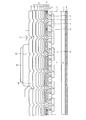
- FIG. 1 is a cross-sectional view showing a configuration of the silicon carbide semiconductor device according to the first embodiment.
- FIG. 2 is a cross-sectional view showing a configuration of the silicon carbide semiconductor device according to the second embodiment.
- FIG. 3 is a cross-sectional view showing the configuration of the silicon carbide semiconductor device according to the third embodiment.
- FIG. 4 is a cross-sectional view showing a configuration of a conventional silicon carbide semiconductor device.
- the semiconductor device according to the present invention is configured using a wide band gap semiconductor.
- a silicon carbide semiconductor device manufactured using, for example, silicon carbide (SiC) as a wide band gap semiconductor will be described using MOSFET as an example.
- FIG. 1 is a cross-sectional view showing a configuration of the silicon carbide semiconductor device according to the first embodiment.
- FIG. 1 illustrates the state of the active region.
- the silicon carbide semiconductor device includes an n + type silicon carbide substrate (first conductivity type wide bandgap semiconductor substrate) 1 on a first main surface (front surface) n.
- a silicon carbide epitaxial layer (first conductivity type wide band gap semiconductor deposition layer) 2 is deposited.
- n + type silicon carbide substrate 1 is a silicon carbide single crystal substrate doped with, for example, nitrogen (N).
- N-type silicon carbide epitaxial layer 2 is a low-concentration n-type drift layer doped with, for example, nitrogen at a lower impurity concentration than n + -type silicon carbide substrate 1.
- n + type silicon carbide substrate 1 and n type silicon carbide epitaxial layer 2 are collectively referred to as a silicon carbide semiconductor substrate.
- MOS gate metal-oxide film-insulated gate made of semiconductor
- the surface layer on the side opposite to the n + -type silicon carbide substrate 1 of the n-type silicon carbide epitaxial layer 2 has ap functioning as a p base layer.
- a + type region (second conductivity type semiconductor region) 10 is selectively provided.
- a p-type silicon carbide epitaxial layer 11 (second conductivity type wide band gap semiconductor layer) is deposited on the surfaces of n-type silicon carbide epitaxial layer 2 and p + -type region 10.
- An n-type well that penetrates p-type silicon carbide epitaxial layer 11 in the depth direction and reaches n-type silicon carbide epitaxial layer 2 is formed in a portion of p-type silicon carbide epitaxial layer 11 on n-type silicon carbide epitaxial layer 2.
- Region 12 (first first conductivity type region) is provided.
- N type well region 12 forms a drift region together with n type silicon carbide epitaxial layer 2.
- n + type source region 4 (second first conductivity type region) is separated from the n type well region 12 in a portion facing the p + type region 10 in the depth direction inside the p type silicon carbide epitaxial layer 11. ) Is selectively provided. Further, a p ++ type contact region 5 (second conductivity type region) having a higher impurity concentration than p type silicon carbide epitaxial layer 11 is selectively between n + type source regions 4 in p type silicon carbide epitaxial layer 11. Is provided.
- a gate electrode 7 is provided on the surface of the portion of p-type silicon carbide epitaxial layer 11 between n + -type source region 4 and n-type well region 12 with gate insulating film 6 interposed therebetween.
- the gate electrode 7 may be provided on the surface of the n-type well region 12 via the gate insulating film 6.
- An interlayer insulating film 13 is provided on the entire front surface side of the silicon carbide semiconductor substrate so as to cover the gate electrode 7.
- a BPSG (Boron Phospho Silicate Glass) film 100 and an NSG (None-doped Silicate Glass) film 101 are laminated.
- the BPSG film 100 is characterized by high adhesion to the gate electrode 7. Further, the BPSG film 100 has a feature that reflow for planarization can be performed at a lower temperature than the PSG film 14. For this reason, the BPSG film 100 is preferably provided on the surface of the gate electrode 7. In addition, since the NSG film 101 is softer than the BPSG film 100, it has a feature that stress due to solder bonding and stress due to a difference in thermal expansion that are concentrated on the stepped portion of the interlayer insulating film 13 can be released. .
- the n + -type source region 4 and the p ++ -type contact region 5 in contact, electrically connected to the n + -type source region 4 and the p ++ -type contact region 5
- a source electrode 8 is provided.
- a first TiN (titanium nitride) film 20 As the source electrode 8, a first TiN (titanium nitride) film 20, a first Ti (titanium) film 21, a second TiN film 22, a second Ti film 23, and an Al—Si film 24 are laminated.
- the Al—Si film 24 is, for example, an aluminum film containing silicon at a rate of 1%.
- the Al—Si film 24 may be an Al—Si—Cu film or an Al—Cu film.
- the Al—Si—Cu film is an aluminum film containing silicon and copper.
- the Al—Cu film is an aluminum film containing copper.
- a drain electrode 9 is provided on the back surface of the silicon carbide semiconductor substrate.
- a protective film 15 is selectively provided on the source electrode 8, and a plating film 16 is provided on the source electrode 8 on which the protective film 15 is not provided.
- the protective film 15 has a function of protecting the front surface of the semiconductor device. Further, the protective film 15 has a function of preventing plating of the plating film 16 from flowing out when forming the plating film 16.
- the protective film 15 has a function of protecting an edge termination structure portion (not shown) surrounding the active region.
- the active region is a region through which a current flows when the semiconductor device is on.
- the edge termination structure portion is a region that is provided so as to surround the periphery of the active region, relaxes the electric field on the substrate front surface side of the drift layer, and maintains a withstand voltage.
- a second protective film 17 is selectively provided so as to cover a portion where the plating film 16 and the protective film 15 are in contact.
- the second protective film 17 covers the gap between the plating film 16 and the protective film 15 and has a function of preventing, for example, solder 19 from entering the substrate side.
- the second protective film 17 functions as a mask when forming the solder 19.
- the second protective film 17 may cover the entire surface of the protective film 15.
- a pin-like electrode 18 is provided which is connected to the plated film 16 portion via a solder 19 and is a wiring material for taking out the potential of the source electrode 8 to the outside.
- the pin-shaped electrode 18 has a needle shape and is joined to the source electrode 8 in an upright state.
- N + type silicon carbide substrate 1 may have a (000-1) plane whose main surface has an off angle of about 4 degrees in the ⁇ 11-20> direction, for example.
- an n-type silicon carbide epitaxial layer 2 having a thickness of 10 ⁇ m doped with nitrogen at an impurity concentration of 1.0 ⁇ 10 16 cm ⁇ 3 is formed on the (000-1) plane of the n + -type silicon carbide substrate 1. Epitaxially grow.
- a mask having a desired opening is formed on the surface of n-type silicon carbide epitaxial layer 2 by a photolithography technique, for example, using a resist.
- p-type impurities for example, aluminum atoms are ion-implanted by ion implantation using this resist mask as a mask.
- p + -type region 10 is formed in a part of the surface region of n-type silicon carbide epitaxial layer 2.
- the mask used at the time of ion implantation for forming the p + -type region 10 is removed.
- p-type silicon carbide epitaxial layer 11 is epitaxially grown on the surface of n-type silicon carbide epitaxial layer 2 to a thickness of 0.5 ⁇ m, for example.
- the p-type silicon carbide epitaxial layer 11 may be epitaxially grown so that the impurity concentration is 2.0 ⁇ 10 16 cm ⁇ 3 .
- a mask having a desired opening is formed on the surface of p-type silicon carbide epitaxial layer 11 by a photolithography technique, for example, using a resist. Then, an n-type impurity such as nitrogen is ion-implanted by ion implantation using this resist mask as a mask. Thereby, n + type source region 4 is formed in a part of the surface region of p type silicon carbide epitaxial layer 11. Next, the mask used at the time of ion implantation for forming the n + -type source region 4 is removed.
- a mask having a desired opening is formed on the surface of p-type silicon carbide epitaxial layer 11 by a photolithography technique, for example, using a resist. Then, a p-type impurity such as aluminum is ion-implanted by ion implantation using this resist mask as a mask. Thereby, p ++ type contact region 5 is formed in part of the surface region of p type silicon carbide epitaxial layer 11. Next, the mask used at the time of ion implantation for forming the p ++ type contact region 5 is removed.
- a mask having a desired opening is formed on the surface of the p-type silicon carbide epitaxial layer 11 by a photolithography technique, for example, with a resist. Then, an n-type impurity such as nitrogen is ion-implanted by ion implantation using this resist mask as a mask. Thereby, n-type well region 12 is formed in a part of the surface region of p-type silicon carbide epitaxial layer 11. Next, the mask used at the time of ion implantation for forming the n-type well region 12 is removed.
- heat treatment for activating the n + -type source region 4, the p ++ -type contact region 5, and the n-type well region 12 is performed.
- the heat treatment temperature and heat treatment time at this time may be 1620 ° C. and 2 minutes, respectively.
- the order of forming the n + -type source region 4, the p ++ -type contact region 5 and the n-type well region 12 can be variously changed.
- the front surface side of the silicon carbide semiconductor substrate is thermally oxidized to form a gate insulating film 6 with a thickness of 100 nm.
- This thermal oxidation may be performed by heat treatment at a temperature of about 1000 ° C. in a mixed atmosphere of oxygen (O 2 ) and hydrogen (H 2 ).
- O 2 oxygen
- H 2 hydrogen
- a polycrystalline silicon layer doped with, for example, phosphorus (P) is formed on the gate insulating film 6 as the gate electrode 7.
- the polycrystalline silicon layer is selectively removed by patterning, leaving the polycrystalline silicon layer on the portion of p-type silicon carbide epitaxial layer 11 sandwiched between n + -type source region 4 and n-type well region 12. .
- a polycrystalline silicon layer may be left on the n-type well region 12. This remaining polycrystalline silicon layer becomes the gate electrode 7.
- a BPSG film 100 is formed as an interlayer insulating film 13 so as to cover the gate electrode 7.
- the BPSG film 100 is made of, for example, boron phosphorous glass (BPSG) with a thickness of 1.0 ⁇ m.
- BPSG boron phosphorous glass
- a reflow process is performed to flatten the BPSG film 100.
- the BPSG film 100 is selectively removed to form a contact hole, and the n + type source region 4 and the p ++ type contact region 5 are exposed.
- a non-doped NSG film 101 is formed on the BPSG film 100.
- the thickness of the NSG film 101 is, for example, about 0.1 ⁇ m.
- the interlayer insulating film 13 is patterned and selectively removed to form a contact hole, exposing the n + -type source region 4 and the p ++ -type contact region 5. Further, after the reflow treatment of the BPSG film 100, a non-doped NSG film 101 is formed on the BPSG film 100, and the interlayer insulating film 13 is selectively removed by patterning to form a contact hole, and an n + type It is also possible to expose the source region 4 and the p ++ type contact region 5. In this case, the number of steps for forming contact holes can be reduced.
- a first TiN film 20, a first Ti film 21, a second TiN film 22, a second Ti film 23, and an Al—Si film 24 are formed.
- the first TiN film 20 is formed by sputtering, and the first Ti film 21 is formed on the first TiN film 20 by sputtering.
- a second TiN film 22 is formed on the first Ti film 21 by sputtering.
- a second Ti film 23 is formed on the second TiN film 22 by sputtering, and an Al—Si film 24 is formed thereon.
- an Al—Si—Cu film or an Al—Cu film may be formed.
- a nickel film for example, is formed as the drain electrode 9 on the surface of the n + type silicon carbide substrate 1 (the back surface of the silicon carbide semiconductor substrate). Then, for example, heat treatment is performed at a temperature of 970 ° C. to form an ohmic junction between the n + -type silicon carbide substrate 1 and the drain electrode 9.
- titanium, nickel (Ni), and gold (Au) are formed in this order as the drain electrode 9 on the surface of the nickel film.
- protective film 15 is selectively formed on source electrode 8 on the front surface side of the silicon carbide semiconductor substrate.
- a plating film 16 is selectively formed on the portion without the protective film 15 on the source electrode 8. Thereby, the plating film 16 is formed on the source electrode 8 without plating flowing to the edge termination structure portion.
- a second protective film 17 is selectively formed using a polymer resin or the like so as to cover a portion where the plating film 16 and the protective film 15 are adjacent to each other.
- the pin-shaped electrode 18 is formed on the plating film 16 via the solder 19. Thereby, the MOSFET shown in FIG. 1 is completed.
- the interlayer insulating film has a two-layer structure of BPSG film / NSG film, whereby stress can be dispersed by the NSG film. Specifically, the adhesion with the gate electrode is enhanced by the BPSG film. In addition, the NSG film can release stress caused by soldering and stress due to a difference in thermal expansion, which are concentrated on the step portion of the interlayer insulating film 13.
- the BPSG film may crack due to stress during solder bonding and stress due to a difference in thermal expansion. Even in this case, the insulation between the gate electrode and the source electrode is maintained by the soft and hard-to-break NSG film, and it is possible to suppress a short circuit between the gate electrode and the source electrode and a failure of the semiconductor device.
- the interlayer insulating film has a two-layer structure of BPSG film / NSG film, hermeticity is improved, and intrusion of a pretreatment liquid when forming a plating film and deterioration of characteristics due to the influence of gas are suppressed. Therefore, a decrease in reliability of the semiconductor device is suppressed.
- a pin-like electrode as a wiring material for extracting the potential of the source electrode to the outside instead of a bonding wire or a plate-like terminal, the pin-like electrode is joined upright to the source electrode and from a direction perpendicular to the chip main surface. An external signal can be taken out.
- FIG. 2 is a cross-sectional view showing a configuration of the silicon carbide semiconductor device according to the second embodiment.
- the semiconductor device according to the second embodiment is different from the semiconductor device according to the first embodiment in that SiN (silicon nitride) is formed on the interlayer insulating film 13, the NSG film 101, or between the BPSG film 100 and the NSG film 101. )
- the film 102 is further laminated to form a three-layer structure.
- the BPSG film 100, the NSG film 101, and the SiN film 102 are sequentially laminated from the gate electrode 7 side. Further, the interlayer insulating film 13 may be laminated in the order of the BPSG film 100, the SiN film 102, and the NSG film 101 from the gate electrode 7.
- the SiN film 102 has a feature that the water absorption is low and water can be prevented from entering the gate electrode 7 side. Further, the SiN film 102 has a feature that the adhesion of the source electrode 8 to the first TiN film 20 is high and it is difficult to peel off from the source electrode 8.
- the BPSG film 100 and the NSG film 101 are formed as the interlayer insulating film 13.
- the SiN film 102 is formed on the NSG film 101.
- the thickness of the SiN film 102 is, for example, about 0.1 ⁇ m. Further, the order of forming the NSG film 101 and the SiN film 102 may be switched.
- the thickness of the BPSG film 100 and the thickness of the NSG film 101 may be made thinner than in the case of the two-layer structure.
- the interlayer insulating film 13 having a three-layer structure may have the same thickness as the interlayer insulating film 13 having a two-layer structure.
- the step of the interlayer insulating film 13 becomes the same level as in the case of the two-layer structure, and the step of the interlayer insulating film 13 can be prevented from becoming larger than in the case of the two-layer structure. It is possible to prevent the sex from becoming worse.
- the BPSG film 100, the NSG film 101, and the SiN film 102 are selectively removed to form contact holes, and the n + type source region 4 and the p ++ type contact region 5 are exposed.
- the MOSFET shown in FIG. 2 is completed by sequentially performing the steps after the step of forming the source electrode 8 as in the first embodiment.
- the silicon carbide semiconductor device and the method for manufacturing the silicon carbide semiconductor device according to the second embodiment the same method as the method for manufacturing the silicon carbide semiconductor device and the silicon carbide semiconductor device according to the first embodiment. An effect can be obtained.
- the silicon carbide semiconductor device and the method for manufacturing the silicon carbide semiconductor device according to the second embodiment for example, by stacking a SiN film on the interlayer insulating film, compared to the case where the interlayer insulating film is two layers, Intrusion of water into the interlayer insulating film can be suppressed, and deterioration of characteristics of the semiconductor device can be prevented. Further, by making the SiN film the uppermost layer of the interlayer insulating film among the BPSG film, NSG film and SiN film of the interlayer insulating film, the adhesion with the TiN film of the source electrode can be enhanced.
- FIG. 3 is a cross-sectional view showing the configuration of the silicon carbide semiconductor device according to the third embodiment.
- the semiconductor device according to the third embodiment is different from the semiconductor device according to the second embodiment in that the SiN film 102 covers the entire surface of the NSG film 101 and the BPSG film 100, so that the BPSG film 100 and the NSG of the interlayer insulating film 13. That is, the end of the film 101 exposed in the contact hole is covered with the SiN film 102.
- the BPSG film 100 and the NSG film 101 are formed as the interlayer insulating film 13.
- the BPSG film 100 and the NSG film 101 are selectively removed to form contact holes, and the n + type source region 4 and the p ++ type contact region 5 are exposed.
- the SiN film 102 is formed on the NSG film 101.
- the thickness of the SiN film 102 is, for example, about 0.1 ⁇ m.
- the SiN film 102 is selectively removed, and the n + type source region 4 and the p ++ type contact region 5 are exposed again to the contact holes.
- the SiN film 102 covers the entire surface of the NSG film 101 and the BPSG film 100, and the end portions of the interlayer insulating film 13 exposed in the contact holes of the BPSG film 100 and the NSG film 101 are covered with the SiN film 102. Is obtained.
- the MOSFET shown in FIG. 3 is completed by sequentially performing the steps after the step of forming the source electrode 8 as in the first embodiment.
- the silicon carbide semiconductor device and the method for manufacturing the silicon carbide semiconductor device according to the third embodiment As described above, according to the silicon carbide semiconductor device and the method for manufacturing the silicon carbide semiconductor device according to the third embodiment, the silicon carbide semiconductor device and the silicon carbide semiconductor device according to the first and second embodiments. Effects similar to those of the manufacturing method can be obtained.
- the end portions exposed to the contact holes of the BPSG film and the NSG film are covered with the SiN film, and the interlayer insulating film Water intrusion can be suppressed.
- the MOSFET has been described as an example.
- the present invention is not limited to this.
- a MOS type semiconductor device such as an IGBT or a semiconductor device configured to cause stress concentration in an element structure due to a step of an interlayer insulating film.
- the present invention can be applied to semiconductor devices having various configurations.
- the case where silicon carbide is used as the wide band gap semiconductor has been described as an example.
- a wide band gap semiconductor other than silicon carbide such as gallium nitride (GaN) is used.
- GaN gallium nitride
- the first conductivity type is n-type and the second conductivity type is p-type.
- the first conductivity type is p-type and the second conductivity type is n-type. It holds. Furthermore, in each of the above-described embodiments, the case where a BPSG film is used as an interlayer insulating film has been described as an example. However, since an NSG film is softer than a PSG (Phospho Silicate Glass) film, the BPSG film is used instead. The same holds true when a PSG film is used.
- the semiconductor device according to the present invention is useful for a high voltage semiconductor device used for a power conversion device, a power supply device such as various industrial machines, and the like. It is suitable for a silicon carbide semiconductor device using a pin-like electrode as a wiring material taken out to the outside.
Landscapes
- Internal Circuitry In Semiconductor Integrated Circuit Devices (AREA)
- Electrodes Of Semiconductors (AREA)
Abstract
半導体装置の、ゲート電極(7)とソース電極(8)を電気的に絶縁する層間絶縁膜(13)は、BPSG膜(100)、NSG膜(101)が順に積層された構造を有する。また、層間絶縁膜(13)は、BPSG膜(100)、NSG膜(101)、SiN膜(102)が順に積層された構造を有する、または、BPSG膜(100)、SiN膜(102)、NSG膜(101)が順に積層された構造を有する。このようにすることで、ピン状電極を半田で接合した半導体装置の信頼性を向上させることができる。
Description
この発明は、半導体装置および半導体装置の製造方法に関する。
従来、高電圧や大電流を制御するパワー半導体装置の構成材料として、シリコン(Si)が用いられている。パワー半導体装置は、バイポーラトランジスタやIGBT(Insulated Gate Bipolar Transistor:絶縁ゲート型バイポーラトランジスタ)、MOSFET(Metal Oxide Semiconductor Field Eeffect Transistor:絶縁ゲート型電界効果トランジスタ)など複数種類あり、これらは用途に合わせて使い分けられている。
例えば、バイポーラトランジスタやIGBTは、MOSFETに比べて電流密度は高く大電流化が可能であるが、高速にスイッチングさせることができない。具体的には、バイポーラトランジスタは数kHz程度のスイッチング周波数での使用が限界であり、IGBTは数十kHz程度のスイッチング周波数での使用が限界である。一方、パワーMOSFETは、バイポーラトランジスタやIGBTに比べて電流密度が低く大電流化が難しいが、数MHz程度までの高速スイッチング動作が可能である。
しかしながら、市場では大電流と高速性とを兼ね備えたパワー半導体装置への要求が強く、IGBTやパワーMOSFETはその改良に力が注がれ、現在ではほぼ材料限界に近いところまで開発が進んでいる。パワー半導体装置の観点からシリコンに代わる半導体材料が検討されており、低オン電圧、高速特性、高温特性に優れた次世代のパワー半導体装置を作製(製造)可能な半導体材料として炭化珪素(SiC)が注目を集めている(下記、非特許文献1参照)。
炭化珪素は、化学的に非常に安定した半導体材料であり、バンドギャップが3eVと広く、高温でも半導体として極めて安定的に使用することができる。また、炭化珪素は、最大電界強度もシリコンより1桁以上大きいため、オン抵抗を十分に小さくすることができる半導体材料として期待される。このような炭化珪素の特長は、他の、シリコンよりバンドギャップが広いワイドバンドギャップ半導体である、例えば窒化ガリウム(GaN)にもあてはまる。このため、ワイドバンドギャップ半導体を用いることにより、半導体装置の高耐圧化を図ることができる(例えば、下記非特許文献2参照)。
このような炭化珪素を用いた高耐圧半導体装置では発生損失が少なくなった分、インバータで使われる際、キャリア周波数が従来のシリコンを用いた半導体装置よりも1桁高い周波数で適用される。半導体装置を高い周波数で適用するとチップへの発熱温度が高くなり、半導体装置への信頼性に影響する。特に、半導体装置のおもて面に露出した電極であるおもて面電極には、おもて面電極の電位を外部に取り出す配線材としてボンディングワイヤが接合されており、半導体装置を高温度で使用すると、おもて面電極とボンディングワイヤとの密着が低下し半導体装置への信頼性に影響を及ぼす。
また、おもて面電極の電位を外部に取り出す別の配線材として、ワイヤボンディング以外に板状導体部材を用いた技術がある(例えば、下記特許文献1参照)。
また、おもて面電極にピン状電極を半田で接合する従来の炭化珪素半導体装置がある。図4は、従来の炭化珪素半導体装置の構成を示す断面図である。n+型炭化珪素基板1の表面にn型炭化珪素エピタキシャル層2が堆積され、n型炭化珪素エピタキシャル層2の表面に複数のp+型領域10が設けられる。p+型領域10の表面にp型炭化珪素エピタキシャル層11が設けられる。p+型領域10が設けられていないn型炭化珪素エピタキシャル層2上のp型炭化珪素エピタキシャル層11にn型ウェル領域12が設けられる。p型炭化珪素エピタキシャル層11の表面には、n+型ソース領域4とp++型コンタクト領域5が設けられる。
p型炭化珪素エピタキシャル層11の、n+型ソース領域4とn型ウェル領域12とに挟まれた表面にゲート絶縁膜6を介して、ゲート電極7が設けられ、ゲート電極7の上部には層間絶縁膜13として、PSG(Phospho Silicate Glass)膜14が選択的に設けられている。n+型ソース領域4とp++型コンタクト領域5との表面に、ソース電極8が設けられる。ソース電極8の上部には、保護膜15が選択的に設けられ、保護膜15が設けられていない部分にめっき膜16が設けられる。
めっき膜16と保護膜15とが隣接する部分を覆うように第2の保護膜17が設けられる。めっき膜16部分に外部信号と接続されるピン状電極18を接続する半田19が設けられる。n+型炭化珪素基板1の裏面側にはドレイン電極9が設けられる。
図4の構造のMOSFETにおいて、ソース電極8に対しドレイン電極9に正の電圧が印加された状態でゲート電極7にゲート閾値以下の電圧が印加されている場合には、p型炭化珪素エピタキシャル層11とn型ウェル領域12とのpn接合が逆バイアスされた状態であり、活性領域の耐圧が確保されて電流は流れない。一方、ゲート電極7にゲート閾値以上の電圧を印加するとゲート電極7直下のp型炭化珪素エピタキシャル層11表面には反転層が形成されることにより電流が流れるため、ゲート電極7に印加する電圧によってMOSFETのスイッチング動作を行うことができる。
ケイ・シェナイ(K.Shenai)、外2名、オプティウム セミコンダクターズ フォー ハイパワー エレクトロニクス(Optimum Semiconductors for High-Power Electronics)、アイ・トリプル・イー トランザクションズ オン エレクトロン デバイシズ(IEEE Transactions on Electron Devices)、1989年9月、第36巻、第9号、p.1811-1823
ビー・ジャヤン・バリガ(B.Jayant Baliga)著、シリコン カーバイド パワー デバイシズ(Silicon Carbide Power Divices)、(米国)、ワールド サイエンティフィック パブリッシング カンパニー(World Scientific Publishing Co.)、2006年3月30日、p.61
しかしながら、従来構造では、層間絶縁膜13の被覆性(ステップカバレッジ)が悪く層間絶縁膜13の表面に下層の凹凸による段差が生じているため、ソース電極8にピン状電極18を半田接合する際に、層間絶縁膜13の段差の部分に応力が集中して掛かる。ここで、層間絶縁膜13の段差とは、層間絶縁膜13がゲート電極7を覆うことにより生じる、n+型炭化珪素基板1とn型炭化珪素エピタキシャル層2とを併せた炭化珪素半導体基体からの層間絶縁膜13の高さである。また、ピン状電極18の半田接合時や半導体装置のスイッチング時に、半田19と周囲との温度差が大きくなるため、半田19の端部付近、特にめっき膜16と保護膜15とソース電極8がお互いに接する3重点部分に熱膨張差により応力が集中する。このように応力が集中することにより、半導体装置の特性が劣化し、信頼性が低下する。最悪の場合、層間絶縁膜13が割れてしまい、ゲート電極7とソース電極8とがショートし、半導体装置が不良になる。
また、めっき膜16を成膜する際の前処理液の侵入、ガスの悪影響により、しきい値電圧が変動するなど半導体装置の特性が劣化し、信頼性が低下する。
この発明は、ピン状電極を半田で接合した半導体装置の信頼性を向上させる半導体装置および半導体装置の製造方法を提供することを目的とする。
上述した課題を解決し、本発明の目的を達成するため、この発明にかかる半導体装置は、次の特徴を有する。この半導体装置は、第1導電型ワイドバンドギャップ半導体基板と、第1導電型ワイドバンドギャップ半導体堆積層と、第2導電型半導体領域と、第2導電型ワイドバンドギャップ半導体層と、第1の第1導電型領域と、第2の第1導電型領域と、ゲート電極と、ソース電極と、層間絶縁膜と、ドレイン電極と、めっき膜と、ピン状電極と、を備える。第1導電型ワイドバンドギャップ半導体基板は、シリコンよりもバンドギャップが広い半導体からなる。第1導電型ワイドバンドギャップ半導体堆積層は、前記第1導電型ワイドバンドギャップ半導体基板のおもて面に堆積され、前記第1導電型ワイドバンドギャップ半導体基板よりも不純物濃度が低い。第2導電型半導体領域は、前記第1導電型ワイドバンドギャップ半導体堆積層の、前記第1導電型ワイドバンドギャップ半導体基板側に対して反対側の表面層に選択的に設けられている。第2導電型ワイドバンドギャップ半導体層は、前記第1導電型ワイドバンドギャップ半導体堆積層および前記第2導電型半導体領域の表面に設けられ、シリコンよりもバンドギャップが広い半導体からなる。第1の第1導電型領域は、前記第2導電型ワイドバンドギャップ半導体層内の前記第1導電型ワイドバンドギャップ半導体堆積層上に選択的に設けられている。第2の第1導電型領域は、前記第2導電型ワイドバンドギャップ半導体層内に選択的に設けられている。ゲート電極は、前記第2の第1導電型領域および前記第1の第1導電型領域の上にゲート絶縁膜を介して設けられている。ソース電極は、前記第2導電型ワイドバンドギャップ半導体層および前記第2の第1導電型領域に接する。層間絶縁膜は、前記ゲート電極を覆う。ドレイン電極は、前記第1導電型ワイドバンドギャップ半導体基板の裏面に設けられている。めっき膜は、前記ソース電極上に、選択的に設けられている。ピン状電極は、前記めっき膜に半田を介して接続され、外部信号をとり出す。そして、前記層間絶縁膜は、第1の絶縁膜と第2の絶縁膜が順に積層された構造を有し、前記第2の絶縁膜は前記第1の絶縁膜に比べて柔らかい材料でできている。
また、この発明にかかる半導体装置は、上述した発明において、前記第1の絶縁膜は、BPSG膜またはPSG膜であり、前記第2の絶縁膜は、NSG膜であることを特徴とする。
また、この発明にかかる半導体装置は、上述した発明において、前記層間絶縁膜は、BPSG膜若しくはPSG膜、NSG膜、SiN膜、または、BPSG膜若しくはPSG膜、SiN膜、NSG膜が順に積層された構造を有することを特徴とする。
また、この発明にかかる半導体装置は、上述した発明において、前記層間絶縁膜は、BPSG膜またはPSG膜、NSG膜、SiN膜が順に積層され、SiN膜がBPSG膜またはPSG膜およびNSG膜の全面を覆い、BPSG膜またはPSG膜およびNSG膜のコンタクトホールに露出した端部がSiN膜で覆われている構造を有することを特徴とする。
また、この発明にかかる半導体装置は、上述した発明において、前記ソース電極は、前記層間絶縁膜と接する部分がTiNからなることを特徴とする。
また、この発明にかかる半導体装置は、上述した発明において、前記ソース電極上に選択的に設けられた保護膜と、前記めっき膜および前記保護膜が接する部分を覆う第2の保護膜と、をさらに備え、前記めっき膜は、前記ソース電極上の前記保護膜が設けられていない部分に、選択的に設けられていることを特徴とする。
上述した課題を解決し、本発明の目的を達成するため、この発明にかかる半導体装置の製造方法は、次の特徴を有する。シリコンよりもバンドギャップが広い半導体からなる第1導電型ワイドバンドギャップ半導体基板のおもて面に、前記第1導電型ワイドバンドギャップ半導体基板よりも不純物濃度の低い第1導電型ワイドバンドギャップ半導体堆積層を形成する工程を含む。前記第1導電型ワイドバンドギャップ半導体堆積層の表面層に、第2導電型半導体領域を選択的に形成する工程を含む。前記第1導電型ワイドバンドギャップ半導体堆積層の表面に、シリコンよりもバンドギャップが広い半導体からなる、第2導電型ワイドバンドギャップ半導体層を形成する工程を含む。前記第2導電型ワイドバンドギャップ半導体層の内部、前記第1導電型ワイドバンドギャップ半導体堆積層上に第1の第1導電型領域を選択的に形成する工程を含む。前記第2導電型ワイドバンドギャップ半導体層の内部に第2の第1導電型領域を選択的に形成する工程を含む。前記第2の第1導電型領域および前記第1の第1導電型領域の上にゲート絶縁膜を介してゲート電極を形成する工程を含む。前記第2導電型ワイドバンドギャップ半導体層および前記第2の第1導電型領域に接するソース電極を形成する工程を含む。前記ゲート電極を覆う層間絶縁膜を形成する工程を含む。前記第1導電型ワイドバンドギャップ半導体基板の裏面にドレイン電極を形成する工程を含む。前記ソース電極上に、選択的にめっき膜を形成する工程を含む。前記めっき膜に半田を介して接続された、外部信号をとり出すピン状電極を形成する工程を含む。そして、前記層間絶縁膜を形成する工程は、第1の絶縁膜と、前記第1の絶縁膜に比べて柔らかい第2の絶縁膜を順に積層する。
上述した発明によれば、層間絶縁膜をBPSG膜/NSG膜の2層構造とすることにより、2層で応力を分散させることができる。具体的は、BPSG膜によりゲート電極との密着性が高くなる。また、NSG膜により段差の部分の応力を逃がすことができる。
このため、ソース電極にピン状電極を接合するために層間絶縁膜の段差の部分に掛かる応力が緩和されることにより、半導体装置の特性劣化が抑制されるため、半導体装置の信頼性の低下が抑制される。また、層間絶縁膜の段差の部分に掛かる応力が緩和されることにより、層間絶縁膜が割れてしまうことを防止できるため、ゲート電極とソース電極とがショートし半導体装置が不良になることを抑制できる。
また、層間絶縁膜を2層構造または3層構造とすることにより、気密性が向上し、めっき膜を成膜する際の前処理液の侵入、ガスの影響による特性劣化が抑制されるため、半導体装置の信頼性の低下が抑制される。また、ボンディングワイヤや板状端子ではなく、ソース電極にピン状電極を半田で接合するため、半導体装置を高温度で使用しても、ソース電極とピン状電極との密着が低下することがなく、半導体装置の信頼性に影響を与えない。
また、層間絶縁膜にSiN膜を積層することにより、ゲート電極側への水の侵入を抑えることができ、半導体装置の特性の劣化を防止できる。また、層間絶縁膜のBPSG膜、NSG膜およびSiN膜の中でSiN膜を最上層に積層することにより、ソース電極のTiN膜との密着性が高くできる。
また、BPSG膜およびNSG膜の端部がSiN膜で覆われることにより、層間絶縁膜への水の侵入を抑えることができる。
本発明にかかる半導体装置および半導体装置の製造方法によれば、半導体装置の特性劣化が抑制され、良好な特性を有する半導体装置を提供することができるという効果を奏する。
以下に添付図面を参照して、この発明にかかる半導体装置および半導体装置の製造方法の好適な実施の形態を詳細に説明する。本明細書および添付図面においては、nまたはpを冠記した層や領域では、それぞれ電子または正孔が多数キャリアであることを意味する。また、nやpに付す+および-は、それぞれそれが付されていない層や領域よりも高不純物濃度および低不純物濃度であることを意味する。+および-を含めたnやpの表記が同じ場合は近い濃度であることを示し濃度が同等とは限らない。なお、以下の実施の形態の説明および添付図面において、同様の構成には同一の符号を付し、重複する説明を省略する。また、本明細書では、ミラー指数の表記において、"-"はその直後の指数につくバーを意味しており、指数の前に"-"を付けることで負の指数をあらわしている。
(実施の形態1)
本発明にかかる半導体装置は、ワイドバンドギャップ半導体を用いて構成される。実施の形態1においては、ワイドバンドギャップ半導体として例えば炭化珪素(SiC)を用いて作製された炭化珪素半導体装置について、MOSFETを例に説明する。図1は、実施の形態1にかかる炭化珪素半導体装置の構成を示す断面図である。図1には、活性領域の状態を図示する。
本発明にかかる半導体装置は、ワイドバンドギャップ半導体を用いて構成される。実施の形態1においては、ワイドバンドギャップ半導体として例えば炭化珪素(SiC)を用いて作製された炭化珪素半導体装置について、MOSFETを例に説明する。図1は、実施の形態1にかかる炭化珪素半導体装置の構成を示す断面図である。図1には、活性領域の状態を図示する。
図1に示すように、実施の形態1にかかる炭化珪素半導体装置は、n+型炭化珪素基板(第1導電型ワイドバンドギャップ半導体基板)1の第1主面(おもて面)にn型炭化珪素エピタキシャル層(第1導電型ワイドバンドギャップ半導体堆積層)2が堆積されている。
n+型炭化珪素基板1は、例えば窒素(N)がドーピングされた炭化珪素単結晶基板である。n型炭化珪素エピタキシャル層2は、n+型炭化珪素基板1よりも低い不純物濃度で、例えば窒素がドーピングされている低濃度n型ドリフト層である。以下、n+型炭化珪素基板1とn型炭化珪素エピタキシャル層2とを併せて炭化珪素半導体基体とする。
炭化珪素半導体基体のおもて面側には、MOSゲート(金属-酸化膜-半導体からなる絶縁ゲート)構造(素子構造)が形成されている。具体的には、n型炭化珪素エピタキシャル層2のn+型炭化珪素基板1に対して反対側(炭化珪素半導体基体のおもて面側)の表面層には、pベース層として機能するp+型領域(第2導電型半導体領域)10が選択的に設けられている。
n型炭化珪素エピタキシャル層2およびp+型領域10の表面には、p型炭化珪素エピタキシャル層11(第2導電型ワイドバンドギャップ半導体層)が堆積されている。また、p型炭化珪素エピタキシャル層11の、n型炭化珪素エピタキシャル層2上の部分には、深さ方向にp型炭化珪素エピタキシャル層11を貫通しn型炭化珪素エピタキシャル層2に達するn型ウェル領域12(第1の第1導電型領域)が設けられている。n型ウェル領域12は、n型炭化珪素エピタキシャル層2とともにドリフト領域を構成する。
p型炭化珪素エピタキシャル層11の内部の、深さ方向にp+型領域10と対向する部分に、n型ウェル領域12と離して、n+型ソース領域4(第2の第1導電型領域)が選択的に設けられている。また、p型炭化珪素エピタキシャル層11内のn+型ソース領域4の間に、p型炭化珪素エピタキシャル層11より高不純物濃度のp++型コンタクト領域5(第2導電型領域)が選択的に設けられている。
p型炭化珪素エピタキシャル層11の、n+型ソース領域4とn型ウェル領域12とに挟まれた部分の表面には、ゲート絶縁膜6を介してゲート電極7が設けられている。ゲート電極7は、ゲート絶縁膜6を介して、n型ウェル領域12の表面に設けられていてもよい。
炭化珪素半導体基体のおもて面側の全面に、ゲート電極7を覆うように層間絶縁膜13が設けられている。層間絶縁膜13として、BPSG(Boron Phospho Silicate Glass)膜100、NSG(None-doped Silicate Glass)膜101が積層されている。
ここで、BPSG膜100は、ゲート電極7との密着性が高いという特徴を有する。また、BPSG膜100は、PSG膜14より低温で平坦化のためのリフローをすることができるという特徴を有する。このため、BPSG膜100は、ゲート電極7の表面に設けられることが好ましい。また、NSG膜101は、BPSG膜100に比べて柔らかいため、層間絶縁膜13の段差部分に集中して掛かる、半田接合する際の応力および熱膨張差による応力を逃がすことができるという特徴を有する。
層間絶縁膜13に開口されたコンタクトホールを介して、n+型ソース領域4およびp++型コンタクト領域5に接し、n+型ソース領域4およびp++型コンタクト領域5と電気的に接続されるソース電極8が設けられている。
ソース電極8として、第1TiN(窒化チタン)膜20、第1Ti(チタン)膜21、第2TiN膜22、第2Ti膜23、Al-Si膜24が積層されている。Al-Si膜24は、例えば、1%割合でシリコンを含んだアルミニウム膜である。
Al-Si膜24は、Al-Si-Cu膜またはAl-Cu膜であってもよい。Al-Si-Cu膜は、シリコンおよび銅を含んだアルミニウム膜である。Al-Cu膜は、銅を含んだアルミニウム膜である。
また、炭化珪素半導体基体の裏面には、ドレイン電極9が設けられている。ソース電極8上に保護膜15が選択的に設けられ、保護膜15が設けられていないソース電極8上にめっき膜16が設けられる。保護膜15は、半導体装置のおもて面を保護する機能を有する。また、保護膜15は、めっき膜16を形成する際、めっき膜16のめっきが外部に流れ出ないようにする機能を有する。また、保護膜15は、活性領域の周囲を囲むエッジ終端構造部(不図示)を保護する機能を有する。ここで、活性領域とは、半導体装置がオン状態のときに電流が流れる領域である。また、エッジ終端構造部とは、活性領域の周囲を囲むように設けられ、ドリフト層の基板おもて面側の電界を緩和し耐圧を保持する領域である。
また、めっき膜16と保護膜15が接する部分を覆うように第2の保護膜17が選択的に設けられる。第2の保護膜17は、めっき膜16と保護膜15との隙間を覆い、例えば半田19などが基体側へ侵入すること防止する機能を有する。第2の保護膜17は、半田19を形成する際のマスクとして機能する。また、第2の保護膜17は、保護膜15の全面を覆ってもよい。また、めっき膜16部分に半田19を介して接続された、ソース電極8の電位を外部に取り出す配線材であるピン状電極18が設けられている。ピン状電極18は、針状の形状を有し、ソース電極8に直立した状態で接合される。
(実施の形態1にかかる炭化珪素半導体装置の製造方法)
次に、実施の形態にかかる炭化珪素半導体装置の製造方法について、例えば、1200Vの耐圧クラスのMOSFETを作成する場合を例に説明する。まず、例えば2×1019cm-3程度の不純物濃度で窒素がドーピングされたn+型炭化珪素基板1を用意する。n+型炭化珪素基板1は、主面が例えば、<11-20>方向に4度程度のオフ角を有する(000-1)面であってもよい。
次に、実施の形態にかかる炭化珪素半導体装置の製造方法について、例えば、1200Vの耐圧クラスのMOSFETを作成する場合を例に説明する。まず、例えば2×1019cm-3程度の不純物濃度で窒素がドーピングされたn+型炭化珪素基板1を用意する。n+型炭化珪素基板1は、主面が例えば、<11-20>方向に4度程度のオフ角を有する(000-1)面であってもよい。
次に、n+型炭化珪素基板1の(000-1)面上に、1.0×1016cm-3の不純物濃度で窒素がドーピングされた厚さ10μmのn型炭化珪素エピタキシャル層2をエピタキシャル成長させる。
次に、n型炭化珪素エピタキシャル層2の表面上に、フォトリソグラフィ技術によって所望の開口部を有するマスクを、例えばレジストで形成する。そして、このレジストマスクをマスクとしてイオン注入法によってp型の不純物、例えばアルミニウム原子をイオン注入する。それによって、n型炭化珪素エピタキシャル層2の表面領域の一部に、p+型領域10が形成される。次に、p+型領域10を形成するためのイオン注入時に用いたマスクを除去する。
次に、n型炭化珪素エピタキシャル層2の表面上に、p型炭化珪素エピタキシャル層11を、例えば0.5μmの厚さでエピタキシャル成長させる。このとき、例えば、p型炭化珪素エピタキシャル層11の不純物濃度が2.0×1016cm-3となるようにエピタキシャル成長させてもよい。
次に、p型炭化珪素エピタキシャル層11の表面上に、フォトリソグラフィ技術によって所望の開口部を有するマスクを、例えばレジストで形成する。そして、このレジストマスクをマスクとしてイオン注入法によってn型の不純物、例えば窒素をイオン注入する。それによって、p型炭化珪素エピタキシャル層11の表面領域の一部に、n+型ソース領域4が形成される。次に、n+型ソース領域4を形成するためのイオン注入時に用いたマスクを除去する。
次に、p型炭化珪素エピタキシャル層11の表面上に、フォトリソグラフィ技術によって所望の開口部を有するマスクを、例えばレジストで形成する。そして、このレジストマスクをマスクとしてイオン注入法によってp型の不純物、例えばアルミニウムをイオン注入する。それによって、p型炭化珪素エピタキシャル層11の表面領域の一部に、p++型コンタクト領域5が形成される。次に、p++型コンタクト領域5を形成するためのイオン注入時に用いたマスクを除去する。
次に、p型炭化珪素エピタキシャル層11の表面上に、フォトリソグラフィ技術によって所望の開口部を有するマスクを、例えばレジストで形成する。そして、このレジストマスクをマスクとしてイオン注入法によってn型の不純物、例えば窒素をイオン注入する。それによって、p型炭化珪素エピタキシャル層11の表面領域の一部に、n型ウェル領域12が形成される。次に、n型ウェル領域12を形成するためのイオン注入時に用いたマスクを除去する。
次に、n+型ソース領域4、p++型コンタクト領域5およびn型ウェル領域12を活性化させるための熱処理(アニール)を行う。このときの熱処理温度および熱処理時間は、それぞれ1620℃および2分間であってもよい。
n+型ソース領域4、p++型コンタクト領域5およびn型ウェル領域12を形成する順序は種々変更可能である。
次に、炭化珪素半導体基体のおもて面側を熱酸化し、ゲート絶縁膜6を100nmの厚さで形成する。この熱酸化は、酸素(O2)と水素(H2)の混合雰囲気中において1000℃程度の温度の熱処理によって行ってもよい。これにより、p型炭化珪素エピタキシャル層11およびn型炭化珪素エピタキシャル層2の表面に形成された各領域がゲート絶縁膜6で覆われる。
次に、ゲート絶縁膜6上に、ゲート電極7として、例えばリン(P)がドープされた多結晶シリコン層を形成する。次に、多結晶シリコン層をパターニングして選択的に除去し、p型炭化珪素エピタキシャル層11のn+型ソース領域4とn型ウェル領域12に挟まれた部分上に多結晶シリコン層を残す。このとき、n型ウェル領域12上に多結晶シリコン層を残してもよい。この残された多結晶シリコン層がゲート電極7となる。
次に、ゲート電極7を覆うように、層間絶縁膜13として、BPSG膜100を形成する。BPSG膜100は、例えば、ボロンリンガラス(BPSG)を1.0μmの厚さで成膜する。次に、BPSG膜100の平担化を行うためにリフロー処理を行う。リフロー処理後、BPSG膜100を選択的に除去して、コンタクトホールを形成し、n+型ソース領域4およびp++型コンタクト領域5を露出させる。次に、BPSG膜100の上にノンドープのNSG膜101を形成する。NSG膜101の厚さは、例えば0.1μm程度である。
次に、層間絶縁膜13をパターニングして選択的に除去することによって、コンタクトホールを形成し、n+型ソース領域4およびp++型コンタクト領域5を露出させる。また、BPSG膜100のリフロー処理後、BPSG膜100の上にノンドープのNSG膜101を形成し、層間絶縁膜13をパターニングして選択的に除去することによって、コンタクトホールを形成し、n+型ソース領域4およびp++型コンタクト領域5を露出させることも可能である。この場合、コンタクトホールを形成する工程を少なくすることができる。
次に、ソース電極8として、第1TiN膜20、第1Ti膜21、第2TiN膜22、第2Ti膜23、Al-Si膜24を形成する。例えば、スパッタ法により第1TiN膜20を形成して、第1TiN膜20上部へスパッタ法により、第1Ti膜21を形成する。次に、第1Ti膜21上部へスパッタ法により、第2TiN膜22を形成する。次に、第2TiN膜22上部へ第2Ti膜23をスパッタ法により形成し、その上部にAl-Si膜24を形成する。Al-Si膜24の代わりに、Al-Si-Cu膜またはAl-Cu膜を形成してもよい。
次に、n+型炭化珪素基板1の表面(炭化珪素半導体基体の裏面)に、ドレイン電極9として、例えばニッケル膜を成膜する。そして、例えば970℃の温度で熱処理し、n+型炭化珪素基板1とドレイン電極9とのオーミック接合を形成する。
次に、ニッケル膜の表面に、ドレイン電極9として例えばチタン、ニッケル(Ni)および金(Au)をこの順に成膜する。次に、炭化珪素半導体基体のおもて面側の、ソース電極8上に選択的に保護膜15を形成する。
次に、保護膜15をマスクとして用いて、ソース電極8上の保護膜15がない部分に、選択的にめっき膜16を形成する。これにより、めっき膜16は、めっきがエッジ終端構造部に流れることなくソース電極8上に形成される。次に、例えば、高分子樹脂等を用いて、めっき膜16と保護膜15とが隣接する部分を覆うように第2の保護膜17を選択的に形成する。
次に、保護膜15および第2の保護膜17を半田付け時のマスクとして用いて、めっき膜16に半田19を介してピン状電極18を形成する。これにより、図1に示したMOSFETが完成する。
以上、説明したように、実施の形態1によれば、層間絶縁膜をBPSG膜/NSG膜の2層構造とすることにより、NSG膜で応力を分散させることができる。具体的には、BPSG膜によりゲート電極との密着性が高くなる。また、NSG膜により、層間絶縁膜13の段差部分に集中して掛かる、半田接合する際の応力および熱膨張差による応力を逃がすことができる。
このように、実施の形態1によれば、半導体装置の特性劣化が抑制されるため、半導体装置の信頼性の低下が抑制される。また、BPSG膜は、半田接合する際の応力および熱膨張差による応力により、割れる場合がある。この場合でも、柔らかく割れにくいNSG膜により、ゲート電極とソース電極との絶縁が維持され、ゲート電極とソース電極とがショートし半導体装置が不良になることを抑制できる。
また、層間絶縁膜をBPSG膜/NSG膜の2層構造とすることにより、気密性が向上し、めっき膜を成膜する際の前処理液の侵入、ガスの影響による特性劣化が抑制されるため、半導体装置の信頼性の低下が抑制される。また、ボンディングワイヤや板状端子ではなく、ソース電極の電位を外部に取り出す配線材をピン状電極とすることで、ソース電極にピン状電極が直立に接合され、チップ主面に垂直な方向から外部信号を取り出すことができる。このため、ワイヤや板状端子を配線材としチップ主面に水平な方向から外部信号を取り出す場合に必要となる電極パッドなどを配置するための領域が不要になり、半導体装置を小型化することができる。また、ソース電極にピン状電極を半田で接合するため、半導体装置を高温度で使用しても、ソース電極とピン状電極との密着が低下することがなく、信頼性に影響を与えない。
(実施の形態2)
図2は、実施の形態2にかかる炭化珪素半導体装置の構成を示す断面図である。実施の形態2にかかる半導体装置が実施の形態1にかかる半導体装置と異なるのは、層間絶縁膜13に、NSG膜101に、または、BPSG膜100とNSG膜101の間に、SiN(窒化シリコン)膜102を、さらに積層して、3層構造にしたことである。
図2は、実施の形態2にかかる炭化珪素半導体装置の構成を示す断面図である。実施の形態2にかかる半導体装置が実施の形態1にかかる半導体装置と異なるのは、層間絶縁膜13に、NSG膜101に、または、BPSG膜100とNSG膜101の間に、SiN(窒化シリコン)膜102を、さらに積層して、3層構造にしたことである。
層間絶縁膜13は、ゲート電極7側から、BPSG膜100、NSG膜101、SiN膜102が順に積層される。また、層間絶縁膜13は、ゲート電極7から、BPSG膜100、SiN膜102、NSG膜101の順に積層されてもよい。
ここで、SiN膜102は、吸水性が低く、ゲート電極7側への水の侵入を抑えることができるという特徴を有する。また、SiN膜102膜は、ソース電極8の第1TiN膜20との密着性が高く、ソース電極8と剥離しにくいという特徴を有する。
(実施の形態2にかかる炭化珪素半導体装置の製造方法)
次に、実施の形態2にかかる炭化珪素半導体装置の製造方法について説明する。まず、実施の形態1と同様に、n型炭化珪素エピタキシャル層2を形成する工程から、ゲート電極7を形成する工程までを順に行う。
次に、実施の形態2にかかる炭化珪素半導体装置の製造方法について説明する。まず、実施の形態1と同様に、n型炭化珪素エピタキシャル層2を形成する工程から、ゲート電極7を形成する工程までを順に行う。
次に、実施の形態1と同様に、層間絶縁膜13として、BPSG膜100、NSG膜101を形成する。次に、NSG膜101の上にSiN膜102を形成する。SiN膜102の厚さは、例えば0.1μm程度である。また、NSG膜101とSiN膜102の形成順番は入れ替わってもかまわない。
また、BPSG膜100の厚さおよびNSG膜101の厚さを2層構造の場合よりも、薄くしてもよい。例えば、3層構造の層間絶縁膜13を2層構造の層間絶縁膜13と同じ程度の厚さにしてもよい。これにより、層間絶縁膜13の段差が2層構造の場合と同じ程度になり、層間絶縁膜13の段差が2層構造の場合より大きくなることを防止することができるため、ソース電極8の被覆性が悪くなることを防ぐことができる。
次に、BPSG膜100、NSG膜101およびSiN膜102を選択的に除去して、コンタクトホールを形成し、n+型ソース領域4およびp++型コンタクト領域5を露出させる。
その後、実施の形態1と同様に、ソース電極8の形成工程以降の工程を順に行うことで、図2に示したMOSFETが完成する。
以上、説明したように、実施の形態2にかかる炭化珪素半導体装置および炭化珪素半導体装置の製造方法によれば、実施の形態1にかかる炭化珪素半導体装置および炭化珪素半導体装置の製造方法と同様の効果を得ることができる。
また、実施の形態2にかかる炭化珪素半導体装置および炭化珪素半導体装置の製造方法によれば、層間絶縁膜が2層の場合に比べて、例えば、層間絶縁膜にSiN膜を積層することにより、層間絶縁膜への水の侵入を抑えることができ、半導体装置の特性の劣化を防止できる。また、層間絶縁膜のBPSG膜、NSG膜およびSiN膜の中でSiN膜を層間絶縁膜の最上層にすることにより、ソース電極のTiN膜との密着性を高くすることができる。
(実施の形態3)
図3は、実施の形態3にかかる炭化珪素半導体装置の構成を示す断面図である。実施の形態3にかかる半導体装置が実施の形態2にかかる半導体装置と異なるのは、SiN膜102がNSG膜101およびBPSG膜100の全面を覆うことにより、層間絶縁膜13のBPSG膜100およびNSG膜101のコンタクトホールに露出した端部が、SiN膜102で覆われていることである。
図3は、実施の形態3にかかる炭化珪素半導体装置の構成を示す断面図である。実施の形態3にかかる半導体装置が実施の形態2にかかる半導体装置と異なるのは、SiN膜102がNSG膜101およびBPSG膜100の全面を覆うことにより、層間絶縁膜13のBPSG膜100およびNSG膜101のコンタクトホールに露出した端部が、SiN膜102で覆われていることである。
(実施の形態3にかかる炭化珪素半導体装置の製造方法)
次に、実施の形態3にかかる炭化珪素半導体装置の製造方法について説明する。まず、実施の形態1と同様に、n型炭化珪素エピタキシャル層2を形成する工程から、ゲート電極7を形成する工程までを順に行う。
次に、実施の形態3にかかる炭化珪素半導体装置の製造方法について説明する。まず、実施の形態1と同様に、n型炭化珪素エピタキシャル層2を形成する工程から、ゲート電極7を形成する工程までを順に行う。
次に、実施の形態1と同様に、層間絶縁膜13として、BPSG膜100、NSG膜101を形成する。次に、BPSG膜100およびNSG膜101を選択的に除去して、コンタクトホールを形成し、n+型ソース領域4およびp++型コンタクト領域5を露出させる。次に、NSG膜101の上にSiN膜102を形成する。SiN膜102の厚さは、例えば0.1μm程度である。次に、SiN膜102を選択的に除去して、コンタクトホールに再度、n+型ソース領域4およびp++型コンタクト領域5を露出させる。ここまでの工程で、SiN膜102がNSG膜101およびBPSG膜100の全面を覆い、層間絶縁膜13のBPSG膜100およびNSG膜101のコンタクトホールに露出した端部が、SiN膜102で覆われている構成が得られる。
その後、実施の形態1と同様に、ソース電極8の形成工程以降の工程を順に行うことで、図3に示したMOSFETが完成する。
以上、説明したように、実施の形態3にかかる炭化珪素半導体装置および炭化珪素半導体装置の製造方法によれば、実施の形態1および実施の形態2にかかる炭化珪素半導体装置および炭化珪素半導体装置の製造方法と同様の効果を得ることができる。
また、実施の形態3にかかる炭化珪素半導体装置および炭化珪素半導体装置の製造方法によれば、BPSG膜およびNSG膜のコンタクトホールに露出した端部がSiN膜で覆われることになり、層間絶縁膜への水の侵入を抑えることができる。
また、本発明の実施の形態では、MOSFETを例に説明したが、これに限らず、IGBTなどのMOS型半導体装置や、層間絶縁膜の段差により素子構造に応力集中が生じる構成の半導体装置など様々な構成の半導体装置に適用可能である。また、上述した各実施の形態では、ワイドバンドギャップ半導体として炭化珪素を用いた場合を例に説明したが、窒化ガリウム(GaN)など炭化珪素以外のワイドバンドギャップ半導体を用いた場合においても同様の効果が得られる。また、各実施の形態では第1導電型をn型とし、第2導電型をp型としたが、本発明は第1導電型をp型とし、第2導電型をn型としても同様に成り立つ。さらには、上述した各実施の形態では、層間絶縁膜としてBPSG膜を用いた場合を例に説明したが、NSG膜はPSG(Phospho Silicate Glass)膜と比べても柔らかいため、BPSG膜の替わりにPSG膜を用いても同様に成り立つ。
以上のように、本発明にかかる半導体装置は、電力変換装置や種々の産業用機械などの電源装置などに使用される高耐圧半導体装置に有用であり、特に、おもて面電極の電位を外部に取り出す配線材としてピン状電極を用いた炭化珪素半導体装置に適している。
1 n+型炭化珪素基板
2 n型炭化珪素エピタキシャル層
4 n+型ソース領域
5 p++型コンタクト領域
6 ゲート絶縁膜
7 ゲート電極
8 ソース電極
9 ドレイン電極
10 p+型領域
11 p型炭化珪素エピタキシャル層
12 n型ウェル領域
13 層間絶縁膜
14 PSG膜
15 保護膜
16 めっき膜
17 第2の保護膜
18 ピン状電極
19 半田
20 第1TiN膜
21 第1Ti膜
22 第2TiN膜
23 第2Ti膜
24 Al-Si膜
100 BPSG膜
101 NSG膜
102 SiN膜
2 n型炭化珪素エピタキシャル層
4 n+型ソース領域
5 p++型コンタクト領域
6 ゲート絶縁膜
7 ゲート電極
8 ソース電極
9 ドレイン電極
10 p+型領域
11 p型炭化珪素エピタキシャル層
12 n型ウェル領域
13 層間絶縁膜
14 PSG膜
15 保護膜
16 めっき膜
17 第2の保護膜
18 ピン状電極
19 半田
20 第1TiN膜
21 第1Ti膜
22 第2TiN膜
23 第2Ti膜
24 Al-Si膜
100 BPSG膜
101 NSG膜
102 SiN膜
Claims (7)
- シリコンよりもバンドギャップが広い半導体からなる第1導電型ワイドバンドギャップ半導体基板と、
前記第1導電型ワイドバンドギャップ半導体基板のおもて面に堆積された、前記第1導電型ワイドバンドギャップ半導体基板よりも不純物濃度の低い第1導電型ワイドバンドギャップ半導体堆積層と、
前記第1導電型ワイドバンドギャップ半導体堆積層の、前記第1導電型ワイドバンドギャップ半導体基板側に対して反対側の表面層に選択的に設けられた第2導電型半導体領域と、
前記第1導電型ワイドバンドギャップ半導体堆積層および前記第2導電型半導体領域の表面に設けられた、シリコンよりもバンドギャップが広い半導体からなる第2導電型ワイドバンドギャップ半導体層と、
前記第2導電型ワイドバンドギャップ半導体層内の前記第1導電型ワイドバンドギャップ半導体堆積層上に選択的に設けられた第1の第1導電型領域と、
前記第2導電型ワイドバンドギャップ半導体層内に選択的に設けられた第2の第1導電型領域と、
前記第2の第1導電型領域および前記第1の第1導電型領域の上にゲート絶縁膜を介して設けられたゲート電極と、
前記第2導電型ワイドバンドギャップ半導体層および前記第2の第1導電型領域に接するソース電極と、
前記ゲート電極を覆う層間絶縁膜と、
前記第1導電型ワイドバンドギャップ半導体基板の裏面に設けられたドレイン電極と、
前記ソース電極上に、選択的に設けられためっき膜と、
前記めっき膜に半田を介して接続された、外部信号をとり出すピン状電極と、
を備え、
前記層間絶縁膜は、第1の絶縁膜と第2の絶縁膜が順に積層された構造を有し、前記第2の絶縁膜は前記第1の絶縁膜に比べて柔らかい材料でできている、
ことを特徴とする半導体装置。 - 前記第1の絶縁膜は、BPSG膜またはPSG膜であり、前記第2の絶縁膜は、NSG膜であることを特徴とする請求項1に記載の半導体装置。
- 前記層間絶縁膜は、BPSG膜若しくはPSG膜、NSG膜、SiN膜、または、BPSG膜若しくはPSG膜、SiN膜、NSG膜が順に積層された構造を有することを特徴とする請求項1に記載の半導体装置。
- 前記層間絶縁膜は、BPSG膜またはPSG膜、NSG膜、SiN膜が順に積層され、前記SiN膜が前記BPSG膜または前記PSG膜および前記NSG膜の全面を覆い、前記BPSG膜または前記PSG膜および前記NSG膜のコンタクトホールに露出した端部が前記SiN膜で覆われている構造を有することを特徴とする請求項1に記載の半導体装置。
- 前記ソース電極は、前記層間絶縁膜と接する部分がTiNからなることを特徴とする請求項1に記載の半導体装置。
- 前記ソース電極上に選択的に設けられた保護膜と、
前記めっき膜および前記保護膜が接する部分を覆う第2の保護膜と、
をさらに備え、
前記めっき膜は、前記ソース電極上の前記保護膜が設けられていない部分に、選択的に設けられていることを特徴とする請求項1~4のいずれか一つに記載の半導体装置。 - シリコンよりもバンドギャップが広い半導体からなる第1導電型ワイドバンドギャップ半導体基板のおもて面に、前記第1導電型ワイドバンドギャップ半導体基板よりも不純物濃度の低い第1導電型ワイドバンドギャップ半導体堆積層を形成する工程と、
前記第1導電型ワイドバンドギャップ半導体堆積層の表面層に、第2導電型半導体領域を選択的に形成する工程と、
前記第1導電型ワイドバンドギャップ半導体堆積層の表面に、シリコンよりもバンドギャップが広い半導体からなる、第2導電型ワイドバンドギャップ半導体層を形成する工程と、
前記第2導電型ワイドバンドギャップ半導体層の内部の、前記第1導電型ワイドバンドギャップ半導体堆積層上に第1の第1導電型領域を選択的に形成する工程と、
前記第2導電型ワイドバンドギャップ半導体層の内部に第2の第1導電型領域を選択的に形成する工程と、
前記第2の第1導電型領域および前記第1の第1導電型領域の上にゲート絶縁膜を介してゲート電極を形成する工程と、
前記第2導電型ワイドバンドギャップ半導体層および前記第2の第1導電型領域に接するソース電極を形成する工程と、
前記ゲート電極を覆う層間絶縁膜を形成する工程と、
前記第1導電型ワイドバンドギャップ半導体基板の裏面にドレイン電極を形成する工程と、
前記ソース電極上に、選択的にめっき膜を形成する工程と、
前記めっき膜に半田を介して接続された、外部信号をとり出すピン状電極を形成する工程と、
を含み、
前記層間絶縁膜を形成する工程は、第1の絶縁膜と、前記第1の絶縁膜に比べて柔らかい第2の絶縁膜を順に積層する、
ことを特徴とする半導体装置の製造方法。
Priority Applications (3)
| Application Number | Priority Date | Filing Date | Title |
|---|---|---|---|
| JP2017539772A JP6347309B2 (ja) | 2015-09-17 | 2016-08-08 | 半導体装置および半導体装置の製造方法 |
| CN201680012697.1A CN107408577B (zh) | 2015-09-17 | 2016-08-08 | 半导体装置及半导体装置的制造方法 |
| US15/686,662 US9997603B2 (en) | 2015-09-17 | 2017-08-25 | Semiconductor device and method of manufacturing semiconductor device |
Applications Claiming Priority (2)
| Application Number | Priority Date | Filing Date | Title |
|---|---|---|---|
| JP2015-184249 | 2015-09-17 | ||
| JP2015184249 | 2015-09-17 |
Related Child Applications (1)
| Application Number | Title | Priority Date | Filing Date |
|---|---|---|---|
| US15/686,662 Continuation US9997603B2 (en) | 2015-09-17 | 2017-08-25 | Semiconductor device and method of manufacturing semiconductor device |
Publications (1)
| Publication Number | Publication Date |
|---|---|
| WO2017047284A1 true WO2017047284A1 (ja) | 2017-03-23 |
Family
ID=58288993
Family Applications (1)
| Application Number | Title | Priority Date | Filing Date |
|---|---|---|---|
| PCT/JP2016/073367 Ceased WO2017047284A1 (ja) | 2015-09-17 | 2016-08-08 | 半導体装置および半導体装置の製造方法 |
Country Status (4)
| Country | Link |
|---|---|
| US (1) | US9997603B2 (ja) |
| JP (1) | JP6347309B2 (ja) |
| CN (1) | CN107408577B (ja) |
| WO (1) | WO2017047284A1 (ja) |
Cited By (4)
| Publication number | Priority date | Publication date | Assignee | Title |
|---|---|---|---|---|
| JP2020126970A (ja) * | 2019-02-06 | 2020-08-20 | 住友電気工業株式会社 | 炭化珪素半導体装置 |
| JP2021061355A (ja) * | 2019-10-08 | 2021-04-15 | 富士電機株式会社 | 半導体装置 |
| WO2023233746A1 (ja) * | 2022-06-03 | 2023-12-07 | 住友電気工業株式会社 | 半導体装置 |
| JP2024123834A (ja) * | 2023-03-02 | 2024-09-12 | 三菱電機株式会社 | 炭化珪素半導体装置及び電力変換装置 |
Families Citing this family (5)
| Publication number | Priority date | Publication date | Assignee | Title |
|---|---|---|---|---|
| JP6561759B2 (ja) * | 2015-10-19 | 2019-08-21 | 富士電機株式会社 | 半導体装置および半導体装置の製造方法 |
| CN106601710B (zh) * | 2015-10-19 | 2021-01-29 | 富士电机株式会社 | 半导体装置以及半导体装置的制造方法 |
| US10998418B2 (en) | 2019-05-16 | 2021-05-04 | Cree, Inc. | Power semiconductor devices having reflowed inter-metal dielectric layers |
| JP7310356B2 (ja) * | 2019-06-27 | 2023-07-19 | 富士電機株式会社 | 半導体装置 |
| EP4064362A1 (en) * | 2021-03-22 | 2022-09-28 | Hitachi Energy Switzerland AG | Power semiconductor device |
Citations (4)
| Publication number | Priority date | Publication date | Assignee | Title |
|---|---|---|---|---|
| JPS6260236A (ja) * | 1985-09-10 | 1987-03-16 | Tdk Corp | 縦形半導体装置およびその製造方法 |
| JP2002334993A (ja) * | 2001-05-09 | 2002-11-22 | Shindengen Electric Mfg Co Ltd | 半導体装置およびその実装方法 |
| JP2012191010A (ja) * | 2011-03-10 | 2012-10-04 | Fuji Electric Co Ltd | 半導体装置およびその製造方法 |
| JP2013232564A (ja) * | 2012-04-27 | 2013-11-14 | National Institute Of Advanced Industrial & Technology | 半導体装置および半導体装置の製造方法 |
Family Cites Families (14)
| Publication number | Priority date | Publication date | Assignee | Title |
|---|---|---|---|---|
| JPH07202185A (ja) * | 1993-12-28 | 1995-08-04 | Sharp Corp | 縦型mosトランジスタの製造方法 |
| US6054752A (en) * | 1997-06-30 | 2000-04-25 | Denso Corporation | Semiconductor device |
| JP4305401B2 (ja) * | 2005-02-28 | 2009-07-29 | セイコーエプソン株式会社 | 半導体装置 |
| JP5774921B2 (ja) * | 2011-06-28 | 2015-09-09 | ルネサスエレクトロニクス株式会社 | 半導体装置、半導体装置の製造方法、及び電子装置 |
| JP5995435B2 (ja) * | 2011-08-02 | 2016-09-21 | ローム株式会社 | 半導体装置およびその製造方法 |
| JP5884557B2 (ja) * | 2012-03-02 | 2016-03-15 | トヨタ自動車株式会社 | 半導体装置 |
| US9722018B2 (en) * | 2012-03-30 | 2017-08-01 | Fuji Electric Co., Ltd. | Vertical high voltage semiconductor apparatus and fabrication method of vertical high voltage semiconductor apparatus |
| US9362392B2 (en) * | 2012-04-24 | 2016-06-07 | Fuji Electric Co., Ltd. | Vertical high-voltage semiconductor device and fabrication method thereof |
| JP6086360B2 (ja) | 2012-04-27 | 2017-03-01 | 国立研究開発法人産業技術総合研究所 | 炭化珪素半導体装置の製造方法 |
| JP2014099444A (ja) | 2012-11-13 | 2014-05-29 | Renesas Electronics Corp | 半導体装置 |
| CN104584221B (zh) * | 2013-02-13 | 2017-04-19 | 富士电机株式会社 | 半导体装置 |
| US9761656B2 (en) * | 2015-04-10 | 2017-09-12 | Macronix International Co., Ltd. | Semiconductor device having buried region and method of fabricating same |
| JP6561759B2 (ja) * | 2015-10-19 | 2019-08-21 | 富士電機株式会社 | 半導体装置および半導体装置の製造方法 |
| JP6705155B2 (ja) * | 2015-11-13 | 2020-06-03 | 富士電機株式会社 | 半導体装置および半導体装置の製造方法 |
-
2016
- 2016-08-08 JP JP2017539772A patent/JP6347309B2/ja active Active
- 2016-08-08 WO PCT/JP2016/073367 patent/WO2017047284A1/ja not_active Ceased
- 2016-08-08 CN CN201680012697.1A patent/CN107408577B/zh active Active
-
2017
- 2017-08-25 US US15/686,662 patent/US9997603B2/en active Active
Patent Citations (4)
| Publication number | Priority date | Publication date | Assignee | Title |
|---|---|---|---|---|
| JPS6260236A (ja) * | 1985-09-10 | 1987-03-16 | Tdk Corp | 縦形半導体装置およびその製造方法 |
| JP2002334993A (ja) * | 2001-05-09 | 2002-11-22 | Shindengen Electric Mfg Co Ltd | 半導体装置およびその実装方法 |
| JP2012191010A (ja) * | 2011-03-10 | 2012-10-04 | Fuji Electric Co Ltd | 半導体装置およびその製造方法 |
| JP2013232564A (ja) * | 2012-04-27 | 2013-11-14 | National Institute Of Advanced Industrial & Technology | 半導体装置および半導体装置の製造方法 |
Cited By (6)
| Publication number | Priority date | Publication date | Assignee | Title |
|---|---|---|---|---|
| JP2020126970A (ja) * | 2019-02-06 | 2020-08-20 | 住友電気工業株式会社 | 炭化珪素半導体装置 |
| JP7180425B2 (ja) | 2019-02-06 | 2022-11-30 | 住友電気工業株式会社 | 炭化珪素半導体装置 |
| JP2021061355A (ja) * | 2019-10-08 | 2021-04-15 | 富士電機株式会社 | 半導体装置 |
| JP7415413B2 (ja) | 2019-10-08 | 2024-01-17 | 富士電機株式会社 | 半導体装置 |
| WO2023233746A1 (ja) * | 2022-06-03 | 2023-12-07 | 住友電気工業株式会社 | 半導体装置 |
| JP2024123834A (ja) * | 2023-03-02 | 2024-09-12 | 三菱電機株式会社 | 炭化珪素半導体装置及び電力変換装置 |
Also Published As
| Publication number | Publication date |
|---|---|
| CN107408577B (zh) | 2020-09-08 |
| JPWO2017047284A1 (ja) | 2018-02-01 |
| JP6347309B2 (ja) | 2018-06-27 |
| US20170352733A1 (en) | 2017-12-07 |
| CN107408577A (zh) | 2017-11-28 |
| US9997603B2 (en) | 2018-06-12 |
Similar Documents
| Publication | Publication Date | Title |
|---|---|---|
| JP6347309B2 (ja) | 半導体装置および半導体装置の製造方法 | |
| JP6561759B2 (ja) | 半導体装置および半導体装置の製造方法 | |
| JP6766889B2 (ja) | 半導体装置および半導体装置の製造方法 | |
| JP6627359B2 (ja) | 半導体装置および半導体装置の製造方法 | |
| JP6052481B2 (ja) | 半導体装置 | |
| JP7087280B2 (ja) | 炭化珪素半導体装置および炭化珪素半導体装置の製造方法 | |
| JP2017079324A (ja) | 半導体装置および半導体装置の製造方法 | |
| JP6863464B2 (ja) | 炭化珪素半導体装置および炭化珪素半導体装置の製造方法 | |
| US10497784B2 (en) | Semiconductor device | |
| JP2015015395A (ja) | 半導体装置及びその製造方法 | |
| JP7243173B2 (ja) | 半導体装置および半導体装置の製造方法 | |
| JP6350760B2 (ja) | 半導体装置および半導体装置の製造方法 | |
| JP7103435B2 (ja) | 半導体装置および半導体装置の製造方法 | |
| JP7415413B2 (ja) | 半導体装置 | |
| JP2020047672A (ja) | 炭化珪素半導体装置および炭化珪素半導体装置の製造方法 |
Legal Events
| Date | Code | Title | Description |
|---|---|---|---|
| 121 | Ep: the epo has been informed by wipo that ep was designated in this application |
Ref document number: 16846157 Country of ref document: EP Kind code of ref document: A1 |
|
| ENP | Entry into the national phase |
Ref document number: 2017539772 Country of ref document: JP Kind code of ref document: A |
|
| NENP | Non-entry into the national phase |
Ref country code: DE |
|
| 122 | Ep: pct application non-entry in european phase |
Ref document number: 16846157 Country of ref document: EP Kind code of ref document: A1 |