WO2017043434A1 - 非接触給電システム - Google Patents
非接触給電システム Download PDFInfo
- Publication number
- WO2017043434A1 WO2017043434A1 PCT/JP2016/075952 JP2016075952W WO2017043434A1 WO 2017043434 A1 WO2017043434 A1 WO 2017043434A1 JP 2016075952 W JP2016075952 W JP 2016075952W WO 2017043434 A1 WO2017043434 A1 WO 2017043434A1
- Authority
- WO
- WIPO (PCT)
- Prior art keywords
- power
- power transmission
- circuit
- mode
- side coil
- Prior art date
Links
- 230000005540 biological transmission Effects 0.000 claims abstract description 571
- 238000012360 testing method Methods 0.000 claims abstract description 249
- 238000001514 detection method Methods 0.000 claims abstract description 182
- 238000000034 method Methods 0.000 claims description 174
- 238000004891 communication Methods 0.000 claims description 170
- 230000008569 process Effects 0.000 claims description 161
- 238000012545 processing Methods 0.000 claims description 72
- 238000011156 evaluation Methods 0.000 claims description 52
- 230000008859 change Effects 0.000 claims description 50
- 238000003384 imaging method Methods 0.000 claims description 10
- 238000001646 magnetic resonance method Methods 0.000 claims description 5
- 230000004044 response Effects 0.000 description 51
- 239000000463 material Substances 0.000 description 40
- 239000003990 capacitor Substances 0.000 description 35
- 230000006870 function Effects 0.000 description 31
- 238000010586 diagram Methods 0.000 description 29
- 230000003287 optical effect Effects 0.000 description 11
- 230000008878 coupling Effects 0.000 description 9
- 238000010168 coupling process Methods 0.000 description 9
- 238000005859 coupling reaction Methods 0.000 description 9
- 238000012790 confirmation Methods 0.000 description 7
- 238000012423 maintenance Methods 0.000 description 6
- 239000000126 substance Substances 0.000 description 6
- 230000007704 transition Effects 0.000 description 6
- 238000004804 winding Methods 0.000 description 6
- 230000003321 amplification Effects 0.000 description 5
- 238000004364 calculation method Methods 0.000 description 5
- 230000007423 decrease Effects 0.000 description 5
- 230000006698 induction Effects 0.000 description 5
- 238000003199 nucleic acid amplification method Methods 0.000 description 5
- 238000009774 resonance method Methods 0.000 description 5
- 238000011282 treatment Methods 0.000 description 5
- 101100219315 Arabidopsis thaliana CYP83A1 gene Proteins 0.000 description 4
- 101000806846 Homo sapiens DNA-(apurinic or apyrimidinic site) endonuclease Proteins 0.000 description 4
- 101000835083 Homo sapiens Tissue factor pathway inhibitor 2 Proteins 0.000 description 4
- XEEYBQQBJWHFJM-UHFFFAOYSA-N Iron Chemical compound [Fe] XEEYBQQBJWHFJM-UHFFFAOYSA-N 0.000 description 4
- 101100269674 Mus musculus Alyref2 gene Proteins 0.000 description 4
- 101100140580 Saccharomyces cerevisiae (strain ATCC 204508 / S288c) REF2 gene Proteins 0.000 description 4
- 102100026134 Tissue factor pathway inhibitor 2 Human genes 0.000 description 4
- 229910052782 aluminium Inorganic materials 0.000 description 4
- XAGFODPZIPBFFR-UHFFFAOYSA-N aluminium Chemical compound [Al] XAGFODPZIPBFFR-UHFFFAOYSA-N 0.000 description 4
- 238000006243 chemical reaction Methods 0.000 description 4
- 238000005259 measurement Methods 0.000 description 4
- 230000009467 reduction Effects 0.000 description 4
- 238000011946 reduction process Methods 0.000 description 4
- 230000005856 abnormality Effects 0.000 description 3
- 238000009795 derivation Methods 0.000 description 3
- 238000013461 design Methods 0.000 description 3
- 238000007689 inspection Methods 0.000 description 3
- 230000003071 parasitic effect Effects 0.000 description 3
- 230000002093 peripheral effect Effects 0.000 description 3
- 239000004065 semiconductor Substances 0.000 description 3
- RYGMFSIKBFXOCR-UHFFFAOYSA-N Copper Chemical compound [Cu] RYGMFSIKBFXOCR-UHFFFAOYSA-N 0.000 description 2
- 230000009471 action Effects 0.000 description 2
- 238000013459 approach Methods 0.000 description 2
- 238000002474 experimental method Methods 0.000 description 2
- 230000002349 favourable effect Effects 0.000 description 2
- 230000020169 heat generation Effects 0.000 description 2
- 229910052742 iron Inorganic materials 0.000 description 2
- 239000004973 liquid crystal related substance Substances 0.000 description 2
- 229910052751 metal Inorganic materials 0.000 description 2
- 239000002184 metal Substances 0.000 description 2
- 238000005457 optimization Methods 0.000 description 2
- 239000011347 resin Substances 0.000 description 2
- 229920005989 resin Polymers 0.000 description 2
- 238000012546 transfer Methods 0.000 description 2
- 238000012935 Averaging Methods 0.000 description 1
- 230000004913 activation Effects 0.000 description 1
- 230000008901 benefit Effects 0.000 description 1
- 230000000295 complement effect Effects 0.000 description 1
- 239000000470 constituent Substances 0.000 description 1
- 229910052802 copper Inorganic materials 0.000 description 1
- 239000010949 copper Substances 0.000 description 1
- 230000003247 decreasing effect Effects 0.000 description 1
- 230000000694 effects Effects 0.000 description 1
- 230000005669 field effect Effects 0.000 description 1
- 238000001914 filtration Methods 0.000 description 1
- 239000011888 foil Substances 0.000 description 1
- 238000011419 induction treatment Methods 0.000 description 1
- 238000003780 insertion Methods 0.000 description 1
- 230000037431 insertion Effects 0.000 description 1
- WABPQHHGFIMREM-UHFFFAOYSA-N lead(0) Chemical compound [Pb] WABPQHHGFIMREM-UHFFFAOYSA-N 0.000 description 1
- 238000004519 manufacturing process Methods 0.000 description 1
- 230000007246 mechanism Effects 0.000 description 1
- 229910044991 metal oxide Inorganic materials 0.000 description 1
- 150000004706 metal oxides Chemical class 0.000 description 1
- 238000012544 monitoring process Methods 0.000 description 1
- 230000002265 prevention Effects 0.000 description 1
- 238000007639 printing Methods 0.000 description 1
- 230000005855 radiation Effects 0.000 description 1
- 238000000926 separation method Methods 0.000 description 1
- 238000003860 storage Methods 0.000 description 1
- 229910000859 α-Fe Inorganic materials 0.000 description 1
Images


Classifications
-
- H—ELECTRICITY
- H02—GENERATION; CONVERSION OR DISTRIBUTION OF ELECTRIC POWER
- H02J—CIRCUIT ARRANGEMENTS OR SYSTEMS FOR SUPPLYING OR DISTRIBUTING ELECTRIC POWER; SYSTEMS FOR STORING ELECTRIC ENERGY
- H02J7/00—Circuit arrangements for charging or depolarising batteries or for supplying loads from batteries
- H02J7/00032—Circuit arrangements for charging or depolarising batteries or for supplying loads from batteries characterised by data exchange
- H02J7/00034—Charger exchanging data with an electronic device, i.e. telephone, whose internal battery is under charge
-
- H—ELECTRICITY
- H02—GENERATION; CONVERSION OR DISTRIBUTION OF ELECTRIC POWER
- H02J—CIRCUIT ARRANGEMENTS OR SYSTEMS FOR SUPPLYING OR DISTRIBUTING ELECTRIC POWER; SYSTEMS FOR STORING ELECTRIC ENERGY
- H02J50/00—Circuit arrangements or systems for wireless supply or distribution of electric power
- H02J50/10—Circuit arrangements or systems for wireless supply or distribution of electric power using inductive coupling
- H02J50/12—Circuit arrangements or systems for wireless supply or distribution of electric power using inductive coupling of the resonant type
-
- H—ELECTRICITY
- H02—GENERATION; CONVERSION OR DISTRIBUTION OF ELECTRIC POWER
- H02J—CIRCUIT ARRANGEMENTS OR SYSTEMS FOR SUPPLYING OR DISTRIBUTING ELECTRIC POWER; SYSTEMS FOR STORING ELECTRIC ENERGY
- H02J50/00—Circuit arrangements or systems for wireless supply or distribution of electric power
- H02J50/60—Circuit arrangements or systems for wireless supply or distribution of electric power responsive to the presence of foreign objects, e.g. detection of living beings
-
- H—ELECTRICITY
- H02—GENERATION; CONVERSION OR DISTRIBUTION OF ELECTRIC POWER
- H02J—CIRCUIT ARRANGEMENTS OR SYSTEMS FOR SUPPLYING OR DISTRIBUTING ELECTRIC POWER; SYSTEMS FOR STORING ELECTRIC ENERGY
- H02J50/00—Circuit arrangements or systems for wireless supply or distribution of electric power
- H02J50/80—Circuit arrangements or systems for wireless supply or distribution of electric power involving the exchange of data, concerning supply or distribution of electric power, between transmitting devices and receiving devices
-
- H—ELECTRICITY
- H02—GENERATION; CONVERSION OR DISTRIBUTION OF ELECTRIC POWER
- H02J—CIRCUIT ARRANGEMENTS OR SYSTEMS FOR SUPPLYING OR DISTRIBUTING ELECTRIC POWER; SYSTEMS FOR STORING ELECTRIC ENERGY
- H02J50/00—Circuit arrangements or systems for wireless supply or distribution of electric power
- H02J50/90—Circuit arrangements or systems for wireless supply or distribution of electric power involving detection or optimisation of position, e.g. alignment
-
- H04B5/26—
-
- H04B5/72—
-
- H04B5/79—
-
- H—ELECTRICITY
- H04—ELECTRIC COMMUNICATION TECHNIQUE
- H04N—PICTORIAL COMMUNICATION, e.g. TELEVISION
- H04N23/00—Cameras or camera modules comprising electronic image sensors; Control thereof
- H04N23/60—Control of cameras or camera modules
- H04N23/698—Control of cameras or camera modules for achieving an enlarged field of view, e.g. panoramic image capture
-
- H—ELECTRICITY
- H04—ELECTRIC COMMUNICATION TECHNIQUE
- H04N—PICTORIAL COMMUNICATION, e.g. TELEVISION
- H04N25/00—Circuitry of solid-state image sensors [SSIS]; Control thereof
- H04N25/70—SSIS architectures; Circuits associated therewith
- H04N25/76—Addressed sensors, e.g. MOS or CMOS sensors
-
- H—ELECTRICITY
- H04—ELECTRIC COMMUNICATION TECHNIQUE
- H04N—PICTORIAL COMMUNICATION, e.g. TELEVISION
- H04N21/00—Selective content distribution, e.g. interactive television or video on demand [VOD]
- H04N21/40—Client devices specifically adapted for the reception of or interaction with content, e.g. set-top-box [STB]; Operations thereof
- H04N21/41—Structure of client; Structure of client peripherals
- H04N21/422—Input-only peripherals, i.e. input devices connected to specially adapted client devices, e.g. global positioning system [GPS]
- H04N21/42204—User interfaces specially adapted for controlling a client device through a remote control device; Remote control devices therefor
- H04N21/42206—User interfaces specially adapted for controlling a client device through a remote control device; Remote control devices therefor characterized by hardware details
- H04N21/42208—Display device provided on the remote control
-
- H—ELECTRICITY
- H04—ELECTRIC COMMUNICATION TECHNIQUE
- H04N—PICTORIAL COMMUNICATION, e.g. TELEVISION
- H04N21/00—Selective content distribution, e.g. interactive television or video on demand [VOD]
- H04N21/40—Client devices specifically adapted for the reception of or interaction with content, e.g. set-top-box [STB]; Operations thereof
- H04N21/41—Structure of client; Structure of client peripherals
- H04N21/422—Input-only peripherals, i.e. input devices connected to specially adapted client devices, e.g. global positioning system [GPS]
- H04N21/42204—User interfaces specially adapted for controlling a client device through a remote control device; Remote control devices therefor
- H04N21/42206—User interfaces specially adapted for controlling a client device through a remote control device; Remote control devices therefor characterized by hardware details
- H04N21/42224—Touch pad or touch panel provided on the remote control
-
- H—ELECTRICITY
- H04—ELECTRIC COMMUNICATION TECHNIQUE
- H04N—PICTORIAL COMMUNICATION, e.g. TELEVISION
- H04N21/00—Selective content distribution, e.g. interactive television or video on demand [VOD]
- H04N21/40—Client devices specifically adapted for the reception of or interaction with content, e.g. set-top-box [STB]; Operations thereof
- H04N21/43—Processing of content or additional data, e.g. demultiplexing additional data from a digital video stream; Elementary client operations, e.g. monitoring of home network or synchronising decoder's clock; Client middleware
- H04N21/442—Monitoring of processes or resources, e.g. detecting the failure of a recording device, monitoring the downstream bandwidth, the number of times a movie has been viewed, the storage space available from the internal hard disk
- H04N21/44213—Monitoring of end-user related data
- H04N21/44222—Analytics of user selections, e.g. selection of programs or purchase activity
- H04N21/44224—Monitoring of user activity on external systems, e.g. Internet browsing
Definitions
- the present invention relates to a non-contact power supply system.
- NFC Near Field Communication
- 13.56 MHz 13.56 MHz
- a technique for performing non-contact power feeding by a magnetic field resonance method using a coil used for NFC communication has also been proposed.
- a power transmission side resonance circuit including a power transmission side coil is arranged in a power supply device (power transmission device) and a power reception side resonance circuit including a power reception side coil is an electronic device as a power reception device (power reception device)
- the resonance frequency of these resonance circuits is set to a common reference frequency.
- an alternating current of a reference frequency is generated in the power transmission side coil by flowing an alternating current through the power transmission side coil in a state where the power reception device (power reception device) is arranged on the power supply base of the power supply device (power transmission device).
- this alternating magnetic field is transmitted to the power receiving side resonance circuit that resonates at the reference frequency, and an alternating current flows through the power receiving side coil. That is, power is transmitted from the power transmission side resonance circuit including the power transmission side coil to the power reception side resonance circuit including the power reception side coil.
- the foreign object here is, for example, an object (such as a card) having a wireless IC tag having an antenna coil of 13.56 MHz that does not respond to NFC communication.
- the foreign object is an electronic device that has the NFC communication function itself but is disabled.
- a smartphone that has an NFC communication function but whose function is turned off by software setting can be a foreign object.
- the smartphone without the power receiving function is classified as a foreign object.
- the foreign object When such a foreign object is placed on the power supply stand, if the power supply device performs a power transmission operation, the foreign object may be destroyed by the strong magnetic field generated by the power transmission coil.
- a strong magnetic field during a power transmission operation may increase the terminal voltage of a foreign object coil on the power supply base from 100 V to 200 V. If no foreign object is formed to withstand such a high voltage, Is destroyed.
- evaluation data that enables determination of the presence or absence of a foreign object is acquired under a predetermined condition, and a power transmission operation may be permitted when it is determined that power transmission is possible based on whether or not power transmission can be performed based on the evaluation data.
- the evaluation data can be obtained only in the flow of “evaluation data acquisition ⁇ transmission execution determination / non-execution control ⁇ transmission execution presence / absence control”, the evaluation data is acquired one after another under various conditions. As a result, it may be difficult to perform efficiently or in detail an evaluation related to the determination of whether or not power transmission can be performed (for example, an evaluation of whether or not the determination is properly performed).
- an object of this invention is to provide the non-contact electric power feeding system which makes it possible to perform efficiently or in detail the evaluation regarding the feasibility determination of power transmission.
- an object of the present invention is to provide a power transmission device for performing contactless power transmission and reception and a contactless power feeding system capable of supporting adjustment of a positional relationship between the power receiving devices.
- a first contactless power supply system includes a power transmission device and a power reception device, and in the contactless power supply system capable of transmitting and receiving power by a magnetic resonance method, the power transmission device transmits the power.
- a power transmission side resonance circuit including a power transmission side coil, a power transmission circuit that generates a magnetic field in the power transmission side coil by supplying an AC voltage to the power transmission side resonance circuit, and a detection that detects an amplitude of a current flowing in the power transmission side coil
- a power transmission side control circuit that operates with any one of a plurality of modes including a first mode and a second mode as an operation mode, and the power reception device includes a power reception side coil for receiving the power.
- a power receiving side resonance circuit Including a power receiving side resonance circuit, a change / short circuit capable of changing a resonance frequency of the power receiving side resonance circuit from a resonance frequency at the time of power reception or a short circuit of the power receiving side coil, and the first mode.
- a power reception side control circuit that operates with any one of a plurality of modes including the second mode as an operation mode, and in the first mode, the power reception side control circuit is a signal by communication from the power transmission device.
- the change / short circuit is used to change the resonance frequency of the power reception side resonance circuit or short circuit the power reception side coil for a predetermined time, and then cancel the change or the short circuit.
- the power transmission circuit is controlled so that a predetermined test magnetic field is generated in the power transmission side coil prior to the power transmission in a period in which the resonance frequency of the power reception side resonance circuit is changed or the power reception side coil is short-circuited, Based on first evaluation data indicating an amplitude detection value of the detection circuit when the test magnetic field is generated in the first mode, it is determined whether or not the power transmission can be performed, and the power transmission is performed.
- the power transmission side control circuit realizes the power transmission by controlling the power transmission circuit so that a power transmission magnetic field larger than the test magnetic field is generated in the power transmission side coil after determining that the power transmission is possible.
- the change / short circuit is used to maintain a change in the resonance frequency of the power reception side resonance circuit or a short circuit of the power reception side coil, and the power transmission side control circuit controls the power transmission circuit to generate the test magnetic field. It is continuously generated by a power transmission side coil, and second evaluation data indicating an amplitude detection value of the detection circuit when the test magnetic field is generated in the second mode is obtained.
- the power transmission side control circuit differs from the power receiving device and generates a magnetic field generated by the power transmission side coil based on the first evaluation data. It is preferable to determine the presence / absence of a foreign substance that can generate a current based on and to control whether or not the power transmission can be performed based on the determination result.
- the power transmission side control circuit determines that the foreign matter does not exist, the power transmission side control circuit permits execution of the power transmission, and the foreign matter When it is determined that there is a power, it is preferable to prohibit execution of the power transmission.
- the power transmission side control circuit determines whether the detected amplitude value indicated by the first evaluation data is out of a predetermined range. It is preferable to determine whether or not the foreign matter exists.
- a processing unit that executes a predetermined process based on the second evaluation data may be further provided in the contactless power feeding system, and the processing unit is provided in the power transmission side control circuit. It may be provided or provided in an external device different from the power transmission device and the power reception device.
- the predetermined process includes a process of displaying the second evaluation data on a display device provided in the power transmission device or connected to the power transmission device. Good to be.
- the predetermined process includes a process of recording the second evaluation data in a recording device provided in the power transmission device or connected to the power transmission device. Also good.
- a processing unit that executes a predetermined process based on the second evaluation data is further provided in the contactless power feeding system, and the processing unit is provided in the power transmission side control circuit. Or provided in an external device different from the power transmitting device and the power receiving device, and the predetermined processing includes a determination as to whether or not an amplitude detection value indicated by the second evaluation data is out of the predetermined range. Also good.
- each of the power transmission side control circuit and the power reception side control circuit changes its operation mode to the second mode when receiving a specific instruction. Otherwise, it is preferable to set its own operation mode to the first mode.
- each of the power transmission device and the power reception device may include an input reception unit for receiving the input of the specific instruction.
- the plurality of modes in the power transmission side control circuit further includes a mode in which the power transmission side coil continuously generates the power transmission magnetic field, and the power receiving
- the plurality of modes in the side control circuit may further include a mode in which the change of the resonance frequency of the power reception side resonance circuit or the short circuit of the power reception side coil is continuously not executed.
- a non-contact power feeding system has a power transmission device having a power transmission side resonance circuit including a power transmission side coil for transmitting power and a power reception side resonance circuit including a power reception side coil for receiving the power.
- the power transmitting device includes a mounting surface on which the power receiving device is to be mounted when the power is transmitted and received.
- a predetermined mark is given to a predetermined position on the mounting surface based on the position of the coil on the power transmission side
- the power receiving device has a camera unit for photographing, and the power receiving device is mounted on the mounting surface.
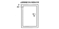
- a control unit that detects the mark on a photographed image obtained by photographing the mark and performs specific notification according to the detection result of the mark before the mark is placed.
- control unit based on the detection result of the mark on the captured image, in the specific notification, a position between the power transmission device and the power reception device in a plane parallel to the placement surface described above. It is advisable to report on the adjustment of the relationship.
- the notification regarding the adjustment of the positional relationship is a necessary movement of the power receiving device with reference to the power transmitting device for power transmission / reception in a plane parallel to the placement surface. It is good to include direction notifications.
- the power receiving device is arranged so that the projected position of the center of the power receiving coil on the mounting surface is within a predetermined area on the mounting surface based on the position of the power transmitting coil.
- the power can be transmitted and received, and the notification relating to the adjustment of the positional relationship is a notification of the necessary moving direction for keeping the projection position within the predetermined area. It is good to contain.
- control unit determines whether or not the projection position is within the predetermined area based on the detection result of the mark on the captured image, and the projection position is within the predetermined area. If not, the necessary movement direction is notified, while if the projection position is within the predetermined area, a predetermined notification different from the notification of the necessary movement direction may be performed.
- execution of the power transmission may be restricted before completion of a predetermined process for performing the specific notification by the control unit.
- the detection result of the mark on the captured image may include a detection result of the position of the mark on the captured image.
- the power receiving device may include a display screen
- the specific notification may include a display on the display screen.
- a housing in the power receiving device has a first surface and a second surface opposite to the first surface, the display screen is provided on the first surface, and the camera unit is configured on the second surface. It is preferable to have an imaging region that starts from the first surface and extends in the direction from the first surface to the second surface.
- the power transmission device acquires current amplitude information of the power transmission side coil when a predetermined magnetic field is generated in the power transmission side coil by supplying an AC voltage to the power transmission side resonance circuit, and the control unit May perform the second specific notification according to the current amplitude information received from the power transmission device via communication.
- the control unit may notify whether the positional relationship between the power transmission device and the power reception device is appropriate, or between the power transmission device and the power reception device. You may alert
- the power transmission device acquires current amplitude information of the power transmission side coil when a predetermined magnetic field is generated in the power transmission side coil by supplying an AC voltage to the power transmission side resonance circuit, and the current amplitude You may perform the 2nd specific alerting
- the power transmission device may notify whether the positional relationship between the power transmission device and the power reception device is appropriate, or between the power transmission device and the power reception device. You may alert
- the non-contact electric power feeding system which makes it possible to perform efficiently or in detail the evaluation regarding the feasibility determination of power transmission.
- the non-contact electric power feeding system which can support adjustment of the positional relationship between a power transmission apparatus and power receiving apparatus for performing non-contact electric power transmission / reception.
- FIG. 4 is a partial configuration diagram of a power supply device including an internal block diagram of an IC in the power supply device according to the first embodiment of the present invention.
- FIG. 3 is a partial configuration diagram of an electronic device including an internal block diagram of an IC in the electronic device according to the first embodiment of the present invention.
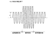
- FIG. 8 is a waveform diagram of a voltage drop of a sense resistor in the load detection circuit of FIG. 7. These are circuit diagrams which show an example of the resonance state change circuit which concerns on 1st Embodiment of this invention. These are circuit diagrams which show the other example of the resonance state change circuit which concerns on 1st Embodiment of this invention.
- (A) And (b) is the schematic external view and schematic internal block diagram of the foreign material which concern on 1st Embodiment of this invention.
- (A)-(d) is a figure which illustrates the arrangement
- FIGS. 1-10 These are figures which concern on 4th Embodiment of this invention and define an X-axis, a Y-axis, and a Z-axis in the relationship with the electric power feeding stand and mounting surface of electric power feeding apparatus.
- (A) And (b) concerns on 4th Embodiment of this invention, and is a figure which shows the center position of the induction
- (A) to (c) are an external perspective view, a side view, and a partial functional block diagram of an electronic apparatus according to a fourth embodiment of the present invention. These are the flowcharts of the induction
- (A) And (b) is a figure which concerns on 4th Embodiment of this invention, and shows the 1st example and 2nd example of the picked-up image acquired by a guidance process.
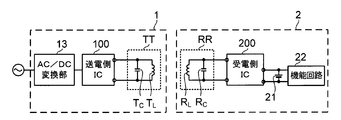
- FIG. 1A and 1B are schematic external views of a power supply device 1 and an electronic device 2 according to the first embodiment of the present invention.
- FIG. 1A is an external view of the power supply device 1 and the electronic device 2 when they are in a separated state
- FIG. 1B is a state where the power supply device 1 and the electronic device 2 are in a reference arrangement state. It is the external view of those times. The significance of the separation state and the reference arrangement state will be described in detail later.
- a contactless power supply system is formed by the power supply device 1 and the electronic device 2.
- the power supply device 1 includes a power plug 11 for receiving commercial AC power and a power supply base 12 formed of a resin material.
- FIG. 2 shows a schematic internal configuration diagram of the power supply device 1 and the electronic device 2.
- the power supply device 1 generates an AC / DC conversion unit 13 that generates and outputs a DC voltage having a predetermined voltage value from a commercial AC voltage input via the power plug 11, and outputs the output voltage of the AC / DC conversion unit 13.
- a power transmission side IC 100 (hereinafter also referred to as IC 100), which is an integrated circuit that is used and driven, and a power transmission side resonance circuit TT (hereinafter also referred to as resonance circuit TT) connected to the IC 100 are provided.
- the AC / DC conversion unit 13, the power transmission side IC 100, and the resonance circuit TT can be arranged in the power supply base 12.
- a circuit that is driven using the output voltage of the AC / DC conversion unit 13 may be provided in the power supply device 1 in addition to the IC 100.
- the electronic device 2 includes a power receiving side IC 200 that is an integrated circuit (hereinafter also referred to as IC 200), a power receiving side resonance circuit RR that is connected to the IC 200 (hereinafter also referred to as resonant circuit RR), and a battery 21 that is a secondary battery. And a functional circuit 22 that is driven based on the output voltage of the battery 21.
- the IC 200 can supply charging power to the battery 21.
- the IC 200 may be driven by the output voltage of the battery 21 or may be driven based on a voltage from a voltage source other than the battery 21.
- a DC voltage obtained by rectifying a signal for NFC communication (details will be described later) received from the power supply device 1 may be the driving voltage of the IC 200.
- the IC 200 can be driven even if the remaining capacity of the battery 21 runs out.
- the electronic device 2 may be any electronic device, such as a mobile phone (including a mobile phone classified as a smart phone), a portable information terminal, a tablet personal computer, a digital camera, an MP3 player, a pedometer, or , A Bluetooth® headset.
- the functional circuit 22 realizes an arbitrary function that the electronic device 2 should realize. Therefore, for example, if the electronic device 2 is a smart phone, the functional circuit 22 transmits / receives information to / from other devices via a call processing unit for realizing a call with the counterpart device and a network. Including a communication processing unit.
- the functional circuit 22 includes a drive circuit that drives the image sensor, an image processing circuit that generates image data from an output signal of the image sensor, and the like.
- the functional circuit 22 may be considered as a circuit provided in an external device of the electronic device 2.
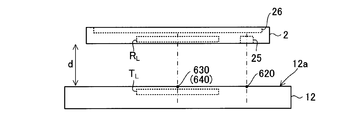
- the resonant circuit TT includes a capacitor T C is a coil T L and the power transmitting side capacitor as the power transmission coil, the resonant circuit RR is the power-receiving-side capacitor and the coil R L a receiver coil And a capacitor RC .
- the power transmission coil T L and a resonant circuit TT by the power transmission side capacitor T C are connected in parallel to each other are formed as a parallel resonance circuit, and the power receiving side coil It is assumed that the resonance circuit RR is formed as a parallel resonance circuit by connecting R L and the power receiving side capacitor RC in parallel.
- the resonant circuit TT by transmitting coil T L and the power-transmitting-side capacitor T C is connected in series with each other may be formed as a series resonant circuit
- the power receiving side coil R L and the power-receiving-side capacitor R C each other The resonance circuit RR may be formed as a series resonance circuit by being connected in series.
- NFC communication Near field communication wireless communication
- the frequency of the communication carrier is 13.56 MHz (megahertz).
- 13.56 MHz is referred to as a reference frequency. Since NFC communication between the devices 1 and 2 is performed by a magnetic field resonance method using the resonance circuits TT and RR, the resonance frequencies of the resonance circuits TT and RR are both set to the reference frequency. However, as will be described later, the resonance frequency of the resonance circuit RR can be temporarily changed from the reference frequency.
- the power transmission and power reception between the devices 1 and 2 are power transmission by NFC from the power supply device 1 to the electronic device 2 and power reception by NFC in the electronic device 2.
- This power transmission and power reception are collectively referred to as NFC power transmission or simply power transmission.
- NFC power transmission By transmitting the power from the coil T L with respect to the coil R L by magnetic field resonance method, the power transmission is achieved in a non-contact manner.
- the state in which the electronic device 2 is placed in a predetermined power transmission area on the power supply stand 12 (the power supply device 1 and the electronic device 2 are in a predetermined positional relationship) and the above-described NFC communication and power transmission can be realized is a reference arrangement state. (Refer to FIG. 1B).
- a state in which the electronic device 2 is sufficiently separated from the power supply stand 12 and cannot realize the above-described NFC communication and power transmission is referred to as a separated state (see FIG. 1A).
- the surface of the power supply base 12 shown in FIG. 1A is flat, a depression or the like that matches the shape of the electronic device 2 to be placed may be formed in the power supply base 12. .
- the reference arrangement state is a state in which the electronic device 2 exists in a predetermined power transmission region (in other words, a region for performing power transmission and power reception) in which power can be transmitted and received between the power supply device 1 and the electronic device 2.
- the belonging and separated state may be understood as belonging to a state in which the electronic device 2 does not exist in the power transmission area.
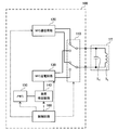
- FIG. 4 shows a partial configuration diagram of the power supply device 1 including an internal block diagram of the IC 100.
- the IC 100 is provided with each part referred to by reference numerals 110, 120, 130, 140, 150 and 160.
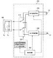
- FIG. 5 shows a configuration diagram of a part of the electronic device 2 including an internal block diagram of the IC 200.
- the IC 200 is provided with each part referred to by reference numerals 210, 220, 230, 240 and 250.
- the capacitor 23 that outputs the driving voltage of the IC 200 may be connected to the IC 200.
- the capacitor 23 can output a DC voltage obtained by rectifying a signal for NFC communication received from the power supply device 1.
- the switching circuit 110 connects either the NFC communication circuit 120 or the NFC power transmission circuit 130 to the resonance circuit TT under the control of the control circuit 160.
- the switching circuit 110 can be configured by a plurality of switches interposed between the resonance circuit TT and the circuits 120 and 130. Any switch described herein may be formed using a semiconductor switching element such as a field effect transistor.
- the switching circuit 210 connects the resonance circuit RR to either the NFC communication circuit 220 or the NFC power receiving circuit 230 under the control of the control circuit 250.
- the switching circuit 210 can be configured by a plurality of switches interposed between the resonance circuit RR and the circuits 220 and 230.
- the state where the resonance circuit TT is connected to the NFC communication circuit 120 via the switching circuit 110 and the resonance circuit RR is connected to the NFC communication circuit 220 via the switching circuit 210 is called a communication connection state.
- NFC communication is possible in the communication connection state.
- the NFC communication circuit 120 can supply an AC signal (AC voltage) having a reference frequency to the resonance circuit TT.
- NFC communication between the devices 1 and 2 is performed in a half-duplex manner.
- NFC communication circuit 220 may transmit any information signal (response signal) from the coil R L of the resonance circuit RR to the coil T L of the resonance circuit TT.
- this transmission is based on the ISO standard (for example, ISO 14443 standard), and is based on a load modulation method that changes the impedance of the coil R L (electronic device side antenna coil) viewed from the coil T L (power supply device side antenna coil). Realized.
- the information signal transmitted from the electronic device 2 is extracted by the NFC communication circuit 120.
- the state where the resonance circuit TT is connected to the NFC power transmission circuit 130 via the switching circuit 110 and the resonance circuit RR is connected to the NFC power reception circuit 230 via the switching circuit 210 is referred to as a power supply connection state.
- the NFC power transmission circuit 130 can perform a power transmission operation, and the NFC power reception circuit 230 can perform a power reception operation.
- Power transmission is realized by power transmission operation and power reception operation.
- the power transmission circuit 130 supplies a power transmission magnetic field (power transmission alternating magnetic field) to the power transmission side coil TL by supplying a power transmission AC signal (power transmission AC voltage) to the resonance circuit TT.
- a power transmission AC signal power transmission AC voltage
- electric power is transmitted from the resonance circuit TT (power transmission side coil T L ) to the resonance circuit RR by the magnetic field resonance method.
- the power received by the power receiving coil RL based on the power transmission operation is sent to the power receiving circuit 230.
- the power receiving circuit 230 In the power receiving operation, the power receiving circuit 230 generates and outputs arbitrary DC power from the received power.
- the battery 21 can be charged with the output power of the power receiving circuit 230.
- NFC communication When NFC communication is performed in the communication connection state, a magnetic field is generated in the coil T L or R L, but the magnetic field strength in the NFC communication is within a predetermined range.
- the lower limit value and the upper limit value of the range are determined by NFC standards, and are 1.5 A / m and 7.5 A / m, respectively.
- the strength of the magnetic field generated in the power transmission side coil TL in the power transmission (that is, the power transmission operation) (the magnetic field strength of the power transmission magnetic field) is larger than the above upper limit, for example, about 45 to 60 A / m. .
- NFC communication and power transmission can be performed alternately, and the state of the magnetic field strength at that time is shown in FIG.
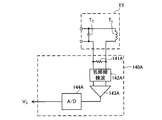
- FIG. 7 shows a relationship among the power transmission circuit 130, the load detection circuit 140, and the resonance circuit TT in the power supply connection state. In FIG. 7, the switching circuit 110 is not shown.
- the power transmission circuit 130 amplifies the sine wave signal generated by the signal generator 131 and the signal generator 131 that generates a sine wave signal of a reference frequency, and the amplified sine wave signal is lined with the potential of the line 134 as a reference.
- An amplifier (power amplifier) 132 that outputs between 134 and 135 and a capacitor 133 are provided.
- the load detection circuit 140 includes a sense resistor 141, an envelope detector 142, an amplifier 143, and an A / D converter 144.
- the signal intensity of the sine wave signal generated by the signal generator 131 is fixed to a constant value, but the amplification factor of the amplifier 132 is variably set by the control circuit 160.
- One end of the capacitor 133 is connected to the line 135.
- the other end of the capacitor 133 are connected in common to one ends of the capacitor T C and coil T L, and the coil T L at the other end another line 134 and the capacitor T C via the sense resistor 141 Commonly connected to the ends.
- the power transmission operation is realized by supplying an AC signal (AC voltage for power transmission) from the amplifier 132 to the resonance circuit TT via the capacitor 133.
- an AC signal from the amplifier 132 is supplied to the resonance circuit TT in the power supply connection state, an AC current having a reference frequency flows in the power transmission side coil TL .
- an AC voltage drop occurs in the sense resistor 141.
- a solid line waveform in FIG. 8 is a voltage waveform of a voltage drop in the sense resistor 141.
- the envelope detector 142 outputs an analog voltage signal proportional to the voltage v in FIG. 8 by detecting the envelope of the voltage drop signal in the sense resistor 141.
- the amplifier 143 amplifies and outputs the output signal of the envelope detector 142.
- the A / D converter 144 outputs a digital voltage value V D by converting the output voltage signal of the amplifier 143 into a digital signal.
- the voltage value V D has a value proportional to the amplitude of the current flowing through the sense resistor 141 (and hence the amplitude of the current flowing through the power transmission side coil TL ) (increase in the amplitude). Along with this, the voltage value V D also increases).
- the load detection circuit 140 is a current amplitude detection circuit that detects the amplitude of the current flowing through the power transmission side coil TL , and it can be considered that the amplitude detection value is the voltage value V D.
- the envelope detector 142 may be provided after the amplifier 143. However, as shown in FIG. 7, it is advantageous to provide the envelope detector 142 in front of the amplifier 143 because it is possible to adopt the amplifier 143 having a lower response performance to a high frequency.
- the load detection circuit 140 detects the magnitude of the load by the output voltage value V D, and can be considered.
- the magnitude of the load here can be said to be the magnitude of the load on the power transmission side coil TL at the time of power transmission, and can also be said to be the magnitude of the load of the electronic device 2 as viewed from the power feeding device 1 at the time of power transmission.
- the sense resistor 141 may be provided inside the IC 100 or may be provided outside the IC 100.
- the memory 150 (see FIG. 4) is composed of a nonvolatile memory, and stores arbitrary information in a nonvolatile manner.
- the control circuit 160 comprehensively controls the operation of each part in the IC 100.
- the control performed by the control circuit 160 includes, for example, control of switching operation of the switching circuit 110, content control and execution presence / absence control of communication operation and power transmission operation by the communication circuit 120 and power transmission circuit 130, operation control of the load detection circuit 140, memory 150 storage controls and read controls are included.
- the control circuit 160 has a built-in timer (not shown) and can measure the time length between arbitrary timings.
- the electronic device 2 in the resonance state changing circuit 240 (see FIG. 5), the other predetermined frequency f M can be changed to a resonant frequency changing circuit from the reference frequency to the resonant frequency of the resonant circuit RR, or the power receiving side coil in the resonance circuit RR This is a coil short circuit capable of short-circuiting RL .
- a resonance frequency changing circuit 240 ⁇ / b> A in FIG. 9 is an example of a resonance frequency changing circuit as the resonance state changing circuit 240.
- the resonance frequency changing circuit 240A includes a series circuit of a capacitor 241 and a switch 242, and one end of the series circuit is commonly connected to one end of each of the capacitor RC and the coil RL , while the other end of the series circuit is the capacitor R. C and the other end of the coil RL are commonly connected.
- the switch 242 is turned on or off under the control of the control circuit 250.
- the resonance circuit RR is formed by only the coil RL and the capacitor RC if the parasitic inductance and the parasitic capacitance are ignored.
- the resonance frequency of the resonance circuit RR matches the reference frequency. That is, when the switch 242 is off, the power receiving side capacitance that determines the resonance frequency of the resonance circuit RR is the capacitor RC itself. Since the capacitor 241 is connected in parallel to the capacitor RC when the switch 242 is on, the resonance circuit RR is formed by the coil RL and the combined capacitance of the capacitors RC and 241. As a result, the resonance circuit RR resonance frequency is low frequency f M than the reference frequency.
- the power receiving side capacitance that determines the resonance frequency of the resonance circuit RR is the above-described combined capacitance.
- the frequency f M is such that the resonance circuit RR does not function as a load on the power transmission side coil TL (ie, enough magnetic resonance does not occur between the resonance circuits TT and RR). It is assumed that it is far from the reference frequency.
- the resonance frequency (that is, the frequency f M ) of the resonance circuit RR when the switch 242 is on is several hundred kHz to 1 MHz.
- the resonance frequency change circuit as changing circuit 240 is not limited to the resonance frequency change circuit 240A, the frequency f M may be higher than the reference frequency.
- the circuit switching the unconnected When the connection is not established, the resonance frequency (>> reference frequency) of the resonance circuit RR is determined by the coil RL and the parasitic capacitance of the wiring).
- the power receiving side resonance circuit RR can be a series resonance circuit.
- the power reception side resonance circuit RR has a parallel circuit or series circuit of a power reception side coil (R L ) and a power reception side capacitance, and the resonance frequency of the power reception side resonance circuit RR when the power reception side capacitance matches a predetermined reference capacitance. f O matches the reference frequency.
- the resonance frequency changing circuit increases or decreases the power receiving side capacitance from the reference capacitance at a necessary timing.
- a parallel circuit or a series circuit is formed by the power receiving side coil (R L ) and the power receiving side capacitance larger or smaller than the reference capacity, and as a result, the resonance frequency of the power receiving side resonance circuit RR.
- f O is changed from the reference frequency.
- a coil short circuit 240B in FIG. 10 is an example of a coil short circuit as the resonance state changing circuit 240.
- the coil short circuit 240B a node where one end of the capacitor RC and one end of the coil RL in the resonance circuit RR are commonly connected, and the other end of the capacitor RC and the other end of the coil RL in the resonance circuit RR are commonly connected.
- the switch 243 is connected (inserted) between the nodes.
- the switch 243 is turned on or off under the control of the control circuit 250. When the switch 243 is turned on, the coil RL in the resonance circuit RR is short-circuited (more specifically, both ends of the coil RL are short-circuited).
- the power receiving side resonance circuit RR does not exist (a state equivalent to a state where the power receiving side resonance circuit RR does not exist). Therefore, while the power receiving coil RL is short-circuited, the load on the power transmitting coil TL is sufficiently lightened (that is, as if the electronic device 2 does not exist on the power supply base 12). As long as the power receiving coil RL can be short-circuited, the coil short-circuit as the changing circuit 240 is not limited to the coil short-circuit 240B.
- the operation of changing the resonance frequency f O of the power reception side resonance circuit RR from the reference frequency in a predetermined frequency f M is called the resonant frequency changing operation, the operation of short-circuit power receiving coil R L by using a coil short circuit This is called a coil short-circuit operation.
- the resonance frequency changing operation or the coil short-circuiting operation may be referred to as f O changing / short-circuiting operation.
- the control circuit 250 comprehensively controls the operation of each part in the IC 200.
- the control performed by the control circuit 250 includes, for example, control of switching operation of the switching circuit 210, content control and execution presence / absence control of communication operation and power reception operation by the communication circuit 220 and power reception circuit 230, and operation control of the change circuit 240. .
- the control circuit 250 has a built-in timer (not shown) and can measure the time length between arbitrary timings. For example, a timer in the control circuit 250, f O changes / short operation due to the resonance frequency f O of the change or the power receiving side time measuring the short-circuit of the coil R L is maintained to a predetermined frequency f M (i.e. below the time T M Measurement; see step S207 in FIG. 19).
- the control circuit 160 of the power supply device 1 can determine whether or not there is a foreign object on the power supply stand 12 and can control the power transmission circuit 130 to perform a power transmission operation only when there is no foreign object.
- Foreign object in the present embodiment is different from the components of the electronic device 2 and the electronic device 2 (such as receiver coil R L), when approaching the feeding device 1, a current based on the magnetic field generated by the transmitting coil T L ( This includes objects that can generate a current in a foreign object.
- the presence of foreign matter may be understood to mean that the foreign matter is present at a position where a non-negligible current flows in the foreign matter based on the magnetic field generated by the power transmission coil TL. .
- the current that has flowed in the foreign matter based on the magnetic field generated by the power transmission side coil TL generates an electromotive force (or counter electromotive force) in the coil ( TL or RL ) that faces and couples to the foreign matter. This can have a non-negligible effect on the characteristics of the circuit including the coil.
- FIG. 11A shows a schematic external view of a foreign material 3 which is a kind of foreign material
- FIG. 11B shows a schematic internal configuration diagram of the foreign material 3.
- the foreign object 3 includes a resonance circuit JJ composed of a parallel circuit of a coil J L and a capacitor J C , and a foreign substance circuit 300 connected to the resonance circuit JJ.
- the resonance frequency of the resonance circuit JJ is set to the reference frequency.
- the foreign material 3 is a device that does not correspond to the power supply device 1.
- the foreign material 3 is an object (such as a non-contact IC card) having a wireless IC tag having an antenna coil (coil J L ) of 13.56 MHz that does not respond to NFC communication.
- the foreign object 3 is an electronic device that has the NFC communication function itself but is disabled.
- a smartphone that has an NFC communication function but whose function is turned off by software setting can be a foreign object 3.
- a smart phone in which the NFC communication function is valid a smart phone that does not have a power receiving function is classified as the foreign object 3.
- a strong magnetic field for example, a magnetic field strength of 12 A / m or more generated by the power transmission side coil TL is generated.
- the foreign matter 3 may be destroyed by the magnetic field having For example, a strong magnetic field during the transmission operation, also have to increase the terminal voltage of the coil J L foreign material 3 on the feeding table 12 up to 100 V ⁇ 200V, foreign body 3 is formed to withstand such a high voltage If not, the foreign material 3 is destroyed.
- FIG. 12 is a flowchart of foreign object detection processing (hereinafter referred to as pFOD processing) executed by the power supply device 1 before power transmission.
- the control circuit 160 When executing the pFOD process, the power transmission circuit 130 is connected to the resonance circuit TT.
- the control circuit 160 first sets the magnetic field strength H by the power transmission side coil TL to a predetermined test strength in step S11.
- the magnetic field strength H is a magnetic field strength generated by the power transmission side coil TL , and more specifically indicates a magnetic field strength of an alternating magnetic field that vibrates at a reference frequency generated by the power transmission side coil TL . Setting the magnetic field strength H to the test strength means that the power transmission circuit 130 is controlled so that a predetermined test AC signal (test AC voltage) is supplied to the resonance circuit TT, thereby having the test strength and the reference frequency.
- the control circuit 160 can variably set the magnetic field strength H by controlling the amplification factor of the amplifier 132 (see FIG. 7).
- a predetermined test AC voltage is supplied to and applied to the resonance circuit TT when the test magnetic field is generated, and a predetermined amplitude having a larger amplitude than the test AC voltage is generated when the power transmission magnetic field is generated.
- the amplification factor of the amplifier 132 may be controlled so that the AC voltage for power transmission is supplied and applied to the resonance circuit TT.
- step S12 the control circuit 160 uses the load detection circuit 140 to acquire the voltage value V D when the test magnetic field is generated as the current amplitude detection value V pFOD .
- Current amplitude detection value V PFOD has a value corresponding to the amplitude of the current flowing through the power transmitting coil T L when to generate a test magnetic field to the power transmission coil T L.
- f O changes / short operation in the electronic apparatus 2 in accordance with an instruction from the power supply apparatus 1 via the NFC communication (resonance frequency change operation or coil short circuit operation) is being performed . Therefore, the resonance circuit RR (power reception side coil R L ) does not substantially function as a load of the power transmission side coil T L and causes no or almost no decrease in the current amplitude detection value V pFOD .
- step S13 the control circuit 160 determines whether or not the current amplitude detection value V pFOD is within a predetermined pFOD normal range.
- the control circuit 160 determines that the foreign material 3 does not exist on the power supply base 12 (step S14). This determination is referred to as foreign object determination.
- the control circuit 160 determines that the foreign material 3 exists on the power supply base 12 (step S15). This determination is referred to as a foreign object determination.
- the control circuit 160 determines that the power transmission operation by the power transmission circuit 130 is possible, permits the power transmission operation (power transmission using the resonance circuit TT), and determines whether there is a foreign object. If it has been established, it is determined that the power transmission operation by the power transmission circuit 130 is impossible, and the execution of the power transmission operation is prohibited. When it is determined that the power transmission operation can be performed, in the power transmission operation, the control circuit 160 can control the power transmission circuit 130 such that a predetermined power transmission magnetic field is generated in the power transmission side coil TL .
- the pFOD normal range is a range that is not less than a predetermined lower limit value V pREFL and not more than a predetermined upper limit value V pREFH (0 ⁇ V pREFL ⁇ V pREFH ). Therefore, when the determination inequality “V pREFL ⁇ V pFOD ⁇ V pREFH ” is satisfied, the foreign object determination is made, and otherwise, the foreign object determination is made.
- the resonance circuit JJ (coil J L ) of the foreign matter 3 functions as a load of the power transmission side coil TL.
- the current amplitude detection value V pFOD is decreased as compared with the case where no foreign matter 3 exists in FIG.
- the foreign material 3a (not shown) different from the foreign material 3 is also considered as a foreign material.
- the foreign material 3a is, for example, a metal body (aluminum foil or aluminum plate) formed including aluminum or a metal body formed including copper.
- the current amplitude detection value V pFOD is less than the lower limit value V pREFL , and the foreign object 3a is present on the power supply table 12. If the current amplitude detection value V pFOD exceeds the upper limit value V pREFH and no foreign matter (3 or 3a) is present on the power supply base 12, the current amplitude detection value V pFOD is pFOD.
- the lower limit value V pREFL and the upper limit value V pREFH are set in advance and stored in the memory 150 through experiments or the like so as to be within the normal range.
- the magnetic field for power transmission is generated in a state where the foreign object 3a exists on the power supply stand 12, the power is absorbed by the foreign object 3a, and the foreign object 3a may generate heat.
- the reference frequency as the carrier frequency of power transmission is 13.56 MHz, it can be said that the possibility of such heat generation is sufficiently small.
- the presence of foreign matter is determined only when the current amplitude detection value V pFOD falls below the lower limit value V pREFL without considering the presence of the foreign matter 3a, and the current amplitude detection value V pFOD is greater than or equal to the lower limit value V pREFL
- the foreign object non- existence determination may be performed (that is, the upper limit value V pREFH may be eliminated).
- the reference frequency in the invention according to the present embodiment is not limited to 13.56 MHz, in the case where the reference frequency, for example, about several 100kHz, because fear of heat generation of the foreign matter 3a is higher, only the lower limit value V PREFL It is desirable to adopt the above-described method in which the upper limit value V pREFH is set to the normal range of pFOD.
- FIG. 13 is an operation flowchart of the initial setting process.
- the initial setting process is executed by the IC 100 under the following initial setting environment.
- the initial setting process may be performed at the time of manufacturing or shipping the power supply device 1. However, if the initial setting environment can be secured, the initial setting process can be performed at an arbitrary timing.
- the power transmission circuit 130 When executing the initial setting process, the power transmission circuit 130 is connected to the resonance circuit TT. Then, in step S21, the magnetic field strength H by the power transmission side coil TL is set to a predetermined test strength, and in the subsequent step S22, the voltage value V D acquired from the A / D converter 144 in the set state is set as the voltage. Obtained as the value V DO . In subsequent step S23, lower limit value V pREFL based on voltage value V DO is stored in memory 150. The lower limit value V pREFL is set to a value lower than the voltage value V DO so that the presence of foreign matter is determined in the pFOD process only in the presence of the foreign matter 3.
- k is a coefficient having a positive predetermined value less than 1. Note that the voltage value V D that would be obtained when the magnetic field strength H is set to a predetermined test strength in the initial setting environment can be estimated at the design stage. Based on the value derived by this estimation, the lower limit value V pREFL may be determined and stored in the memory 150 without performing the initial setting process.
- the load on the power transmission side coil T L is sufficiently lightly (That is, it is as if the electronic device 2 does not exist on the power supply stand 12), and the current amplitude detection value V pFOD becomes sufficiently large to determine that there is no foreign object.
- the resonance frequency of the resonance circuit RR is changed to the frequency f M or the power reception side coil RL is short-circuited, the foreign matter 3 continues to exist as a load of the power transmission side coil TL. For this reason (because the resonance frequency of the resonance circuit JJ of the foreign material 3 remains the reference frequency), the current amplitude detection value V pFOD becomes sufficiently small and foreign matter determination is made.
- the power supply device 1 can determine whether or not the electronic device 2 that can support power transmission exists on the power supply base 12 by NFC communication.
- the state in which the foreign object 3 is present on the power supply base 12 is not limited to the state in which the foreign object 3 is in direct contact with the power supply base 12. For example, as shown in FIG. 15, a foreign object presence determination is also made in a state where the electronic device 2 exists in direct contact with the power supply stand 12 and the foreign material 3 exists on the electronic device 2. As long as the foreign object 3 exists on the power supply stand 12, it belongs.
- the power supply device 1 is a transmission side and the electronic device 2 is a reception side, and the power supply device 1 (IC 100) transmits an inquiry signal 510 to a device on the power supply base 2 (hereinafter also referred to as a power supply target device) by NFC communication.
- the power supply target device includes the electronic device 2 and may include the foreign material 3.
- the inquiry signal 510 is, for example, a signal for inquiring unique identification information of a power supply target device, a signal for inquiring whether the power supply target device is in a state where NFC communication can be performed, and whether the power supply target device can receive power or transmit power. It includes a signal that asks if you are seeking
- the electronic device 2 (IC 200) that has received the inquiry signal 510 transmits a response signal 520 that answers the inquiry content of the inquiry signal 510 to the power supply device 1 by NFC communication.
- the power supply device 1 (IC 100) that has received the response signal 520 analyzes the response signal 520, and if the power supply target device is capable of NFC communication and can receive power or requests power transmission, a test request
- the signal 530 is transmitted to the power supply target device by NFC communication.
- the electronic device 2 (IC 200) as the power supply target device that has received the test request signal 530 transmits a response signal 540 to the test request signal 530 to the power supply device 1 by NFC communication, and then promptly changes the f O / A short-circuit operation (resonance frequency changing operation or coil short-circuit operation) is executed.
- the test request signal 530 is a signal for requesting and instructing execution of the f O change / short circuit operation
- the control circuit 250 of the electronic device 2 receives the test request signal 530 as an opportunity to change / short circuit the f O
- the operation is executed by the resonance state changing circuit 240.
- the f O change / short-circuit operation is not executed.
- f O changes / short test request signal 530 if the trigger for the execution of the operation may be any signal, or may be contained in the inquiry signal 510.
- the power supply apparatus 1 (IC 100) that has received the response signal 540 executes the above-described pFOD process.
- the electronic device 2 (IC 200) continues to execute the f 2 O change / short-circuit operation.
- the electronic device 2 (IC 200) is built-in timer with, f O changes / short since maintaining the execution of only f O changes / short operation time corresponding to the length of the execution period of pFOD process Stop operation.
- the power supply device 1 transmits an authentication signal 550 to the power supply target device by NFC communication.
- the authentication signal 550 includes, for example, a signal for notifying the power supply target device that power transmission will be performed from now on.
- the electronic device 2 (IC 200) that has received the authentication signal 550 transmits a response signal 560 corresponding to the authentication signal 550 to the power supply device 1 by NFC communication.
- the response signal 560 includes, for example, a signal notifying that the content indicated by the authentication signal 550 has been recognized or a signal giving permission to the content indicated by the authentication signal 550.
- the power supply device 1 (IC 100) that has received the response signal 560 executes the power transmission operation by connecting the power transmission circuit 130 to the resonance circuit TT, thereby realizing the power transmission 570.
- the power transmission 570 is executed according to the above flow. However, in the second case of FIG. 14B, the process proceeds until the transmission / reception of the response signal 540. Since it is determined that there is a foreign object on the power supply stand 12 in the pFOD process, the power transmission 570 is not executed.
- One power transmission 570 may be performed only for a predetermined time, and a series of processing from transmission of the inquiry signal 510 to power transmission 570 may be repeatedly executed.
- NFC communication, pFOD processing, and power transmission NFC power transmission
- NFC power transmission can be executed sequentially and repeatedly. That is, in the non-contact power supply system, the operation of performing NFC communication, the operation of performing pFOD processing, and the operation of performing power transmission (NFC power transmission) can be repeatedly performed in order in a time division manner.
- FIG. 18 is an operation flowchart of the power supply device 1. The operations of the communication circuit 120 and the power transmission circuit 130 are executed under the control of the control circuit 160.
- step S101 the control circuit 160 connects the communication circuit 120 to the resonance circuit TT through the control of the switching circuit 110.
- the control circuit 160 transmits an inquiry signal 510 to the power supply target device by NFC communication using the communication circuit 120 and the resonance circuit TT, and then waits for reception of the response signal 520 in step S103.
- the control circuit 160 analyzes the response signal 520, and the power supply target device is capable of NFC communication and can receive power or request power transmission.
- step S104 Y in step S104
- the process proceeds to step S105. Otherwise (N in step S104), the process returns to step S102.
- step S105 the control circuit 160 transmits the test request signal 530 to the power supply target device by NFC communication using the communication circuit 120 and the resonance circuit TT, and then waits for reception of the response signal 540 in step S106.
- the control circuit 160 connects the power transmission circuit 130 to the resonance circuit TT through the control of the switching circuit 110, and in the subsequent step S108, the above-described pFOD process is performed. Do.
- step S109 the control circuit 160 connects the communication circuit 120 to the resonance circuit TT through the control of the switching circuit 110, and proceeds to step S110.
- step S108 if foreign matter determination is made, the process returns from step S110 to step S102, but if foreign matter non-judgment is made, the process proceeds from step S110 to step S111.
- step S111 the control circuit 160 transmits the authentication signal 550 to the power supply target device by NFC communication using the communication circuit 120 and the resonance circuit TT, and then waits for reception of the response signal 560 in step S112.
- step S113 the control circuit 160 connects the power transmission circuit 130 to the resonance circuit TT through the control of the switching circuit 110, and proceeds to step S114.
- the control circuit 160 sets the power transmission permission flag to ON in step S114, starts the power transmission operation and the mFOD process, and then proceeds to step S115.
- step S115 the presence or absence of a foreign object during power transmission is detected by the mFOD process, and when a foreign object is detected, the power transmission permission flag is turned off.
- the control circuit 160 measures the elapsed time from the start time of the power transmission operation, and compares the elapsed time with a predetermined time t A (for example, 10 minutes) and checks the state of the power transmission permission flag in step S115. When the elapsed time reaches a predetermined time t A or when the power transmission permission flag is set to OFF by the mFOD process, the process proceeds to step S116.
- step S116 the control circuit 160 switches the power transmission permission flag from ON to OFF or maintains the power transmission permission flag OFF, stops the power transmission operation and the mFOD process, and then returns to step S101.
- FIG. 19 is an operation flowchart of the electronic device 2, and the process starting from step S201 is executed in conjunction with the operation of the power supply device 1 shown in FIG.
- the operations of the communication circuit 220 and the power receiving circuit 230 are executed under the control of the control circuit 250.
- step S201 the control circuit 250 connects the communication circuit 220 to the resonance circuit RR through the control of the switching circuit 210.
- the f O change / short-circuit operation is not executed when the electronic device 2 is activated.
- step S202 control circuit 250 uses communication circuit 220 and waits for reception of inquiry signal 510.
- step S203 the control circuit 250 analyzes the inquiry signal 510 to generate a response signal 520, and generates the response signal 520 by NFC communication using the communication circuit 220. Transmit to the power supply device 1.
- the control circuit 250 confirms the state of the battery 21, and if the battery 21 is not fully charged and no abnormality is recognized in the battery 21, a signal for receiving power or requesting power transmission is sent to the response signal 520. include. On the other hand, if battery 21 is fully charged or if abnormality is recognized in battery 21, a signal indicating that power cannot be received is included in response signal 520.
- step S205 the control circuit 250 transmits a response signal 540 to the feeding apparatus 1 by the NFC communication using the communication circuit 220, perform a f O changes / short operation using a resonance state changing circuit 240 at the subsequent step S206 To do. That is, short-circuiting or the power receiving coil R L changes from the reference frequency of the resonance frequency f O to the frequency f M.
- the control circuit 250 measures the time elapsed from the start of the f O changes / short operation (step S207), and stops the f O changes / short operation when the elapsed time reaches the predetermined time t M ( Step S208).
- the resonance frequency f O is returned to the reference frequency or the short circuit of the power receiving coil RL is eliminated. Thereafter, the process proceeds to step S209.
- f O changes / short run operations is maintained, promptly f O changes / short the end of that time operation time t M as stopped is preset.
- the time t M may be specified in the test request signal 530.
- step S209 the control circuit 250 waits for reception of the authentication signal 550 using the communication circuit 220.
- the control circuit 250 transmits a response signal 560 to the authentication signal 550 to the power supply device 1 by NFC communication using the communication circuit 220 in step S 210. If a foreign object exists on the power supply stand 12, the authentication signal 550 is not transmitted from the power supply device 1 (see step S110 in FIG. 18). Therefore, if the authentication signal 550 is not received for a predetermined time in step S209. It is good to return to step S201.
- step S211 the control circuit 250 connects the power reception circuit 230 to the resonance circuit RR through the control of the switching circuit 210, and starts a power reception operation using the power reception circuit 230 in step S212.
- the control circuit 250 measures the time elapsed from the start of the power receiving operation, and compares the elapsed time with a predetermined time t B (step S213). Then, the elapsed time reaches the time t B (Y in step S213), in step S214, the control circuit 250, a power receiving operation is stopped and the flow returns to step S201.
- the time t B is predetermined or specified in the authentication signal 550 so that the period during which the power receiving operation is performed substantially coincides with the period during which the power transmission operation is performed in the power supply device 1. .
- the control circuit 250 monitors the charging current to the battery 21 and determines that the power transmission operation is terminated when the charging current value becomes equal to or lower than the predetermined value. You may make it perform transfer to.
- a foreign object may be placed on the power supply stand 12 after the power transmission operation is started.
- the mFOD process functions as a foreign object detection process during power transmission, and the presence or absence of a foreign object is continuously monitored during power transmission by the mFOD process.
- FIG. 20 is an operation flowchart of the mFOD process.
- the control circuit 160 repeatedly executes the mFOD process in FIG. 20 during the period during which the power transmission operation is performed.
- the control circuit 160 first acquires the latest voltage value V D as the current amplitude detection value V MFOD step S51.
- Current amplitude detection value V MFOD has a value corresponding to the amplitude of the current flowing through the power transmitting coil T L when is generating power for the magnetic field to the power transmission coil T L.
- the control circuit 160 determines whether or not the current amplitude detection value V mFOD belongs to a predetermined mFOD normal range.
- step S53 When the current amplitude detection value V mFOD belongs to the mFOD normal range, the foreign object non-determination is determined (step S53), the process returns to step S51, and the processing of steps S51 and S52 is repeated, but the current amplitude detection value V mFOD is mFOD.
- step S54 the foreign matter presence determination is made in step S54, and the power transmission permission flag is set to OFF.
- the power transmission permission flag is a flag managed by the control circuit 160 and is set to ON or OFF. When the power transmission permission flag is ON, the control circuit 160 permits the execution of the power transmission operation, and when the power transmission permission flag is OFF, the control circuit 160 prohibits the execution of the power transmission operation or stops the power transmission operation.
- the mFOD normal range is a range not less than a predetermined lower limit value V mREFL and not more than a predetermined upper limit value V mREFH (0 ⁇ V mREFL ⁇ V mREFH ). Therefore, when the determination inequality “V mREFL ⁇ V mFOD ⁇ V mREFH ” is satisfied, the foreign object determination is made, and otherwise, the foreign object determination is made.
- the foreign material 3 formed as a non-contact IC card is inserted between the power supply base 12 of the power supply device 1 and the electronic device 2.
- the coil J L of the power receiving coil R L and foreign substances 3 of the electronic device 2 is magnetically coupled, resonant frequency is the reference frequency of the resonant circuit RR of the electronic device 2 together with the resonance frequency of the resonance circuit JJ foreign matter 3 Deviation from (13.56 MHz).
- the power received by the power receiving side coil RL decreases, and the load of power transmission viewed from the power transmitting side coil TL becomes lighter.
- the upper limit value V mREFH may be determined so that “V mREFH ⁇ V mFOD ”.
- a foreign material 3 b as an iron plate or a ferrite sheet is inserted between the power supply base 12 of the power supply device 1 and the electronic device 2.
- a current flows in the foreign matter 3b through the electrical and magnetic action, and as a result, the amplitude of the current flowing in the power transmission side coil TL is reduced (in this case, the lower limit is such that “V mFOD ⁇ V mREFL ”).
- the value V mREFL may be determined).
- the current amplitude detection value V mFOD changes depending on the presence or absence of the foreign matter including the foreign matters 3 and 3b.
- the lower limit value V MREFL and the upper limit value V MREFH may be stored in the memory 150. Further, it is estimated by theoretical calculation how much the current amplitude detection value V mFOD changes due to the presence of a foreign substance during power transmission, and based on the estimation result, the lower limit value V mREFL is not required.
- the upper limit value V mREFH may be determined and stored in the memory 150. At this time, for example, an object that changes the current amplitude detection value V mFOD by a predetermined change rate or more with reference to the center value of the mFOD normal range may be defined as a foreign object.
- the amplification factor of the amplifier 143 shown in FIG. 7 is variable.
- the amplitude of the current flowing through the power transmitting coil T L is than when performing pFOD treatment, is much To larger when performing the power transmission operation and mFOD process. Therefore, the control circuit 160 sets the amplification factor of the amplifier 143 smaller when performing the mFOD process than when performing the pFOD process, thereby setting the input signal range of the A / D converter 144 between the pFOD process and the mFOD process. Same level.
- the envelope detector 142 and the A / D converter 144 may be inserted between the two.
- amplitude information obtained by performing high-frequency reduction processing in other words, averaging processing or low-pass filtering
- V D voltage value
- the high-frequency reduction process is a process for reducing (attenuating) a relatively high frequency signal component while allowing a relatively low frequency signal component in the voltage drop signal of the sense resistor 141 to pass.
- a high-frequency reduction process is performed on the voltage value V D generated by the output signal of the A / D converter 144.
- the voltage value V D after the high-frequency reduction process may be used as the current amplitude detection value V mFOD (the same may be applied to the current amplitude detection value V pFOD in the pFOD process).
- the high frequency reduction processing by calculation is processing executed by the control circuit 160, and passes a relatively low frequency signal component in the output signal of the A / D converter 144, while relatively high frequency signal component. This is a process for reducing (attenuating).
- the role of the mFOD process is not limited only to the presence / absence determination of foreign matter.
- the mFOD process has a role of turning off the power transmission permission flag under any circumstances inappropriate for continuation of the power transmission operation such that the current amplitude detection value V mFOD deviates from the mFOD normal range.
- the power transmission permission flag is turned OFF (step S54 in FIG. 20).
- control circuit 160 controls whether or not the power transmission is continued by monitoring whether or not the current amplitude detection value V mFOD is out of the mFOD normal range when power is being transmitted by the power transmission operation. To do. As a result, since the power transmission operation is stopped through the mFOD process in a situation inappropriate for the continuation of the power transmission operation, such as when a foreign object is placed on the power supply stand 12 after the power transmission operation is started, the foreign material due to the continuation of the power transmission operation is stopped. Can be avoided.
- Second Embodiment A second embodiment of the present invention will be described.
- the second embodiment is an embodiment based on the first embodiment.
- the description of the first embodiment is applied to the second embodiment as long as there is no contradiction.
- control circuit 160 in the power supply device 1 operates in an operation mode set by setting one of a plurality of modes including the normal mode and the test mode as its own operation mode.
- control circuit 250 in the electronic device 2 operates in an operation mode set by setting any one of a plurality of modes including a normal mode and a test mode as its own operation mode.
- the plurality of modes for the control circuit 160 and the plurality of modes for the control circuit 250 may be the same or different from each other.
- the plurality of modes for the control circuit 160 and the control circuit 250 can include modes other than the normal mode and the test mode, but only the normal mode and the test mode will be noted below.
- the operations of the power supply device 1 and the electronic device 2 described in the first embodiment are all operations when the operation mode of the control circuits 160 and 250 is set to the normal mode (except for the initial setting process). .
- the control circuit 160 of the power supply device 1 changes its operation mode only when receiving a predetermined test mode setting instruction at the time of starting the power supply device 1 or at any timing after the power supply device 1 is started. Set to test mode, otherwise set own operation mode to normal mode. Similarly, the control circuit 250 of the electronic device 2 only has its own input when a predetermined test mode setting instruction is input when the electronic device 2 is activated or at any timing after the electronic device 2 is activated. The operation mode is set to the test mode, otherwise the operation mode is set to the normal mode.
- power supply device 1 has an input receiving unit 170 for receiving input of various instructions including a test mode setting instruction, and electronic device 2 receives input of various instructions including a test mode setting instruction.
- the input receiving unit 170 may be configured by one or more push button switches, for example.
- the test mode setting instruction is sent to the power supply device 1.
- the push button switch that can be included in the input receiving unit 170 may be a button on the touch panel.
- the input reception unit 170 may be configured by a communication port that can receive a signal transmitted from an external device.
- receiving a predetermined test mode transition request signal from an external device at the communication port of the input receiving unit 170 corresponds to inputting a test mode setting instruction to the power supply device 1 and the input receiving unit 170,
- the operation mode of the control circuit 160 is set to the test mode.
- the external device is a device different from the power supply device 1 and the electronic device 2, and may be a computer device 4 (see FIG. 23) described later, for example.
- the input receiving unit 270 may be configured by one or more push button switches, for example.
- the test mode setting instruction is issued to the electronic device 2.
- the push button switch that can be included in the input receiving unit 270 may be a button on the touch panel.
- the input reception unit 270 may be configured by a communication port that can receive a signal transmitted from an external device.
- receiving a predetermined test mode transition request signal from an external device at the communication port of the input receiving unit 270 corresponds to inputting a test mode setting instruction to the electronic device 2 and the input receiving unit 270.
- the operation mode of the control circuit 250 is set to the test mode.
- the operation mode After the operation mode is set to the test mode in the control circuit 160 of the power supply device 1, when the power supply device 1 is turned off and the power supply device 1 is restarted, the operation mode becomes the normal mode.
- the control circuit 160 sets its own operation mode to the test mode and then satisfies a predetermined condition (for example, when receiving an input of a normal mode transition instruction different from the test mode setting instruction at the input receiving unit 170) It may be possible to shift the operation mode to the normal mode.
- the operation mode becomes the normal mode when the power of the electronic device 2 is turned off and the electronic device 2 is restarted. Further, the control circuit 250 itself sets the operation mode to the test mode and then establishes a predetermined condition (for example, when the input reception unit 270 receives an input of a normal mode transition instruction different from the test mode setting instruction). It may be possible to shift the operation mode to the normal mode.
- the control circuit 250 continuously executes the f O change / short-circuit operation using the resonance state change circuit 240. That is, the state where the resonance frequency f O of the resonance circuit RR is changed to the frequency f M or the state where the power receiving side coil RL is short-circuited is maintained. This maintenance is maintained as long as the operation mode of the control circuit 250 is the test mode.
- the time t M (see step S207 in FIG.
- the resonance circuit RR may be connected to the communication circuit 220 or the power receiving circuit 230 via the switching circuit 210.
- the control circuit 160 causes the resonance circuit TT to pass through the switching circuit 110 through control to the switching circuit 110 and the power transmission circuit 130.
- the amplitude of the current flowing through the power transmission coil TL is continuously detected, and the detection result is obtained as the voltage value V D (see FIG. 7).
- the voltage value V D obtained when the power transmission side coil TL generates the test magnetic field in the test mode (that is, the current amplitude detection value of the power transmission side coil TL by the detection circuit 140) is particularly called a test mode detection value.
- V TEST As long as the test mode is maintained, the test mode detection value V TEST is periodically acquired (for example, acquired at intervals of 1 millisecond).
- the non-contact power feeding system includes a processing unit that executes a predetermined test process based on the test mode detection value V TEST .
- This processing unit may be provided in the control circuit 160 of the power supply device 1 or may be provided in an external device different from the power supply device 1 and the electronic device 2. Here, it is assumed that the processing unit is provided in an external device. You may think that an external apparatus is contained in the component of a non-contact electric power feeding system.
- FIG. 23 shows the external appearance of the computer device 4 as an example of the external device together with the external appearance of the power supply device 1.
- FIG. 24 is a schematic internal block diagram of the computer apparatus 4.
- the computer device 4 includes parts referred to by reference numerals 41 to 44.
- the arithmetic processing unit 41 includes a CPU (Central Processing Unit), a ROM (Read Only Memory), a RAM (Random Access Memory), and the like.
- the arithmetic processing unit 41 executes various arithmetic processes and supervises the operation of each part in the computer device 4. Control.
- the display unit 42 includes a liquid crystal display panel or the like, and displays arbitrary information as a video under the control of the arithmetic processing unit 41.
- the recording unit 43 includes a magnetic disk and a semiconductor memory, and records arbitrary information.
- the communication processing unit 44 performs wireless or wired communication between the computer apparatus 4 and a different device.
- wired communication according to a predetermined wired communication standard (for example, USB (Universal Serial Bus) standard) is possible between the power supply device 1 and the computer apparatus 4, and a communication port provided in the power supply device 1.
- a communication port provided in the computer device 4 are connected by a predetermined communication cable, so that any information can be bidirectionally communicated between the power supply device 1 and the computer device 4.
- a predetermined wired communication standard for example, USB (Universal Serial Bus) standard
- V TEST including transmission
- the value V TEST may be wireless communication.
- FIG. 25 is an operation flowchart of the power supply device 1 in the test mode.
- the power transmission circuit 130 is connected to the resonance circuit TT.
- the magnetic field strength H by the power transmission side coil TL is set to a predetermined test strength.
- V D is obtained as a test mode detection value V TEST .
- the control circuit 160 transmits the obtained test mode detection value V TEST to the computer apparatus 4 via a communication port provided in the power supply device 1. Thereafter, the processes in steps S72 and S73 are periodically repeated.
- the arithmetic processing unit 41 can execute a predetermined test process based on the test mode detection value V TEST .
- the test process may include a process of displaying the test mode detection value V TEST on the display unit 42.
- the test mode detection value V TEST itself or a value obtained by subjecting the test mode detection value V TEST to a predetermined calculation may be displayed on the display unit 42, or the test mode detection
- the time series data of the value V TEST or the time series data of values obtained by performing a predetermined calculation on the test mode detection value V TEST may be graphed and displayed on the display unit 42.
- the test process may include a process for causing the recording unit 43 to record the test mode detection value V TEST .
- the test unit detection value V TEST itself or a value obtained by applying a predetermined calculation (for example, predetermined four arithmetic operations) to the test mode detection value V TEST may be recorded in the recording unit 43. Since the test mode detection value V TEST obtained periodically and sequentially, the time-series data of the value obtained by performing a predetermined operation on the time-series data or test mode detection value V TEST test mode detection value V TEST, recording unit 43 You can make it record.
- the test process may include a determination as to whether or not the test mode detection value V TEST falls within the normal pFOD range described in the first embodiment (see FIG. 12). This determination result may be displayed on the display unit 42.
- the control circuit 160 may also determine whether or not the test mode detection value V TEST is within the normal range of pFOD, and the determination result indicates the light emission that can be provided in the power supply device 1. You may make it express in light emission modes, such as a diode.
- Test mode detection value V TEST to be tested for treatment a test mode detection value V TESTA acquired when disposed only electronic device 2 of the test mode in a predetermined transmission area on the feed table 12, the test The test mode detection value V TESTB acquired when the electronic device 2 in the mode and the foreign object (for example, the foreign object 3) are arranged in a predetermined power transmission area on the power supply stand 12 may be included. If there is no abnormality in the power supply device 1 and the electronic device 2 in the test mode, the former test mode detection value V TESTA should be within the pFOD normal range, and the latter test mode detection value V TESTB is within the pFOD normal range. Should deviate.
- the pFOD process and the power transmission are alternately and repeatedly executed when the electronic device 2 is placed on the power supply stand 12 (see FIG. 17). At this time, one power transmission is performed for several minutes to several hours. One pFOD process is completed in about 100 milliseconds.
- the presence / absence of a foreign object is determined in each pFOD process, but there are cases where it is desired to evaluate whether the determination of the presence / absence of a foreign object is performed as desired under various circumstances.
- the foreign matter determination is actually made under various situations where the foreign matter determination should be made (under the situation of FIG. 14B or FIG. 15).
- test mode the same situation as when the pFOD process is performed in the normal mode is continuously realized, and the test mode detection corresponding to the current amplitude detection value V pFOD (see FIG. 12) obtained by the pFOD process in the normal mode is performed.
- the value V TEST can be efficiently acquired under various acquisition conditions. That is, for example, the test mode detection values V TESTA and V TESTB can be sequentially obtained in the test mode, and whether or not the test mode detection values V TESTA and V TESTB are within the normal range of pFOD is determined through the test process. Check it.
- the first test mode detection value V TEST is acquired in the first state in which the electronic device 2 is placed at a predetermined position on the power supply stand 12 and the foreign object 3 is placed at a predetermined position away from the power supply stand 12. It is also possible to acquire the second test mode detection value V TEST in the second state in which the electronic device 2 and the foreign material 3 are placed at the first and second predetermined positions on the table 12. For example, in the first state, if no foreign matter determination should be made, it may be confirmed through the test process whether the first test mode detection value V TEST falls within the normal range of pFOD. If foreign matter determination should be made in this state, it may be confirmed through the test processing whether the second test mode detection value V TEST deviates from the pFOD normal range.
- the operation confirmation related to the foreign object detection process before power transmission (evaluation of whether or not the foreign object detection process before power transmission is properly performed) can be performed efficiently and in detail. Can be performed.
- the arithmetic processing unit 41 that executes a predetermined test process based on the test mode detection value V TEST is provided in the control circuit 160. May be.
- the display unit 42 is provided in the computer device 4, it can be said that the display unit 42 is connected to the power supply device 1 via the communication processing unit 44, but the display unit 42 is not the computer device 4 but the power supply device. 1 may be provided.
- the recording unit 43 is provided in the computer device 4, it can be said that the recording unit 43 is connected to the power supply device 1 via the communication processing unit 44. You may make it provide in the apparatus 1.
- the third embodiment is an embodiment based on the first and second embodiments. Regarding matters not specifically described in the third embodiment, the description of the first and second embodiments is the third unless there is a contradiction. This also applies to the embodiment. In the third embodiment, the description of the third embodiment is given priority regarding matters that contradict between the third embodiment and the first or second embodiment.
- modes MA1 to MA4 are provided as test modes of control circuit 160 in power supply device 1, and modes MB1 and MB2 are provided as test modes of control circuit 250 in electronic device 2. It has been.
- the control circuit 160 of the power supply device 1 receives a predetermined first to fourth test mode setting instruction when the power supply device 1 is started or at any timing after the power supply device 1 is started.
- the own operation mode is set to each of modes MA1 to MA4. Otherwise, the own operation mode is set to the normal mode.
- the control circuit 250 of the electronic device 2 receives input of predetermined first and second test mode setting instructions when the electronic device 2 is activated or at an arbitrary timing after the electronic device 2 is activated. When this occurs, its own operation mode is set to modes MB1 and MB2, respectively, and otherwise its own operation mode is set to the normal mode.
- the input of each test mode setting instruction is preferably received by the input receiving units 170 and 270 (see FIG. 22).
- the mode MB1 is the test mode itself described in the second embodiment.
- the control circuit 250 In the mode MB1 (that is, when the operation mode of the control circuit 250 is set to the mode MB1), the control circuit 250 The f O change / short circuit operation is continuously executed using the resonance state change circuit 240. That is, the state where the resonance frequency f O of the resonance circuit RR is changed to the frequency f M or the state where the power receiving side coil RL is short-circuited is maintained. This maintenance is maintained as long as the operation mode of the control circuit 250 is the mode MB1.
- the time t M (see step S207 in FIG.
- the resonance circuit RR may be connected to the communication circuit 220 or the power receiving circuit 230 via the switching circuit 210.
- mode MB2 In mode MB2 (ie, when the operation mode of the control circuit 250 is set to mode MB2), the control circuit 250 continuously disables the f O change / short-circuit operation, and thus the resonance frequency of the resonance circuit RR. f O is maintained at the reference frequency. This maintenance is maintained as long as the operation mode of the control circuit 250 is the mode MB2.
- the resonance circuit RR In mode MB2, the resonance circuit RR is connected to the power receiving circuit 230 via the switching circuit 210. That is, in mode MB2, electronic device 2 is in the same state as when a power receiving operation is performed.
- the control circuit 160 switches the resonance circuit TT through control to the switching circuit 110 and the power transmission circuit 130.
- the test magnetic field is generated in the power transmission side coil TL by being connected to the power transmission circuit 130 via the circuit 110 and supplying and applying a predetermined test AC voltage from the power transmission circuit 130 to the resonance circuit TT. Maintain the state. This maintenance is maintained as long as the operation mode of the control circuit 160 is the mode MA1 or MA2. That is, in the modes MA1 and MA2, the control circuit 160 continuously generates the test magnetic field in the power transmission side coil TL through the control to the switching circuit 110 and the power transmission circuit 130.
- the control circuit 160 In the modes MA3 and MA4 (that is, when the operation mode of the control circuit 160 is set to the mode MA3 or MA4), the control circuit 160 causes the resonance circuit TT to pass through the control to the switching circuit 110 and the power transmission circuit 130.
- a state where the power transmission circuit 130 is connected via the switching circuit 110 and a predetermined AC voltage for power transmission is supplied and applied from the power transmission circuit 130 to the resonance circuit TT so that the power transmission magnetic field is generated in the power transmission coil TL . Maintain the state that is occurring. This maintenance is maintained as long as the operation mode of the control circuit 160 is the mode MA3 or MA4. That is, in the modes MA3 and MA4, the control circuit 160 continuously generates the power transmission magnetic field in the power transmission side coil TL through the control to the switching circuit 110 and the power transmission circuit 130.
- the amplitude of the current flowing through the power transmission side coil TL is continuously detected, and the detection result is obtained as a voltage value V D (see FIG. 7).
- the voltage value V D (that is, the current amplitude detection value of the power transmission side coil TL by the detection circuit 140) obtained in the modes MA1 to MA4 is particularly called a test mode detection value.
- the voltage value V D obtained when the power transmission side coil TL generates a test magnetic field in the mode MA1 or MA2 is represented by the symbol V TEST , and the power transmission side coil TL transmits power in the mode MA3 or MA4.
- a voltage value V D obtained when the magnetic field for generation is generated is represented by a symbol V TEST2 .
- test mode detection value V TEST is periodically acquired.
- test mode detection value V TEST2 is periodically acquired (for example, acquired at an interval of 1 millisecond).
- the test mode detection values V TEST or V TEST2 acquired sequentially may be transmitted to the arithmetic processing unit 41 via the communication processing unit 44 of FIG.
- the test mode detection value V TEST is the same as the test mode detection value V TEST described in the second embodiment. Therefore, when the operation mode of the control circuit 160 is set to the mode MA1 or MA2, the non-contact power feeding system performs various operations in the test mode described in the second embodiment (including the operation of FIG. 25 and the test process). May be realized. Even when the operation mode of the control circuit 160 is set to the mode MA3 or MA4, the operation and test processing of FIG. 25 can be applied and executed. However, when the operation and test processing of FIG.
- the operation mode of the control circuit 160 is set to the mode MA1 and the above-described initial setting environment is prepared (that is, neither the electronic device 2 nor the foreign object is placed on the power supply base 12). Based on the test mode detection value V TEST obtained in this state, the above-described value V pREFL can be set (see FIG. 13).
- the operation mode of the control circuit 160 is set to the mode MA1 and the electronic device 2 in the mode MB1 is placed on the power supply base 12.
- the arithmetic processing unit 41 can evaluate whether or not the f O change / short-circuit operation is correctly executed based on the test mode detection value V TEST obtained in this state. For example, when the difference between the detection value V TEST obtained by the first and the detected value V TEST obtained in the test mode a second test mode is less than a predetermined value, f O changes / short operation is correctly performed If not, it is determined that the f O change / short-circuit operation is not correctly executed. Ideally, the detection value V TEST obtained in the first test form is equal to the detection value V TEST obtained in the second test form.
- the operation mode of the control circuit 160 is set to the mode MA2 and the above-described initial setting environment is prepared (that is, neither the electronic device 2 nor the foreign object is placed on the power supply base 12). Based on the test mode detection value V TEST obtained in this state, the above-described value V pREFL can be set (see FIG. 13).
- the third test configuration is equivalent to the first test configuration described above.
- the operation mode of the control circuit 160 is set to the mode MA2, and the electronic device 2 and the foreign material 3 in the mode MB1 are placed on the power supply base 12.
- the test mode detection value V TEST obtained in this state whether the foreign matter 3 is correctly determined for the presence of the foreign matter 3 in the arithmetic processing unit 41 (the presence of the foreign matter 3 in the pFOD process in the normal mode)
- the margin uses the detection value V TEST obtained in the fourth test form (however, the detection value when the foreign material 3 is placed on the power supply base 12 as a foreign material), and the difference (V pREFL ⁇ V TEST).
- the operation mode of the control circuit 160 is set to the mode MA2, and the electronic device 2 and the foreign material 3a (such as an aluminum plate) in the mode MB1 are placed on the power supply base 12.
- the test mode detection value V TEST obtained in this state, whether or not the foreign matter 3a is correctly determined for the presence of the foreign matter 3a in the arithmetic processing unit 41 (the presence of the foreign matter 3a in the pFOD process in the normal mode)
- the presence of the foreign matter 3a in the pFOD process in the normal mode On the other hand, whether or not a foreign object presence determination is correctly made is confirmed, and a margin is confirmed.
- the margin in this case is the difference (V TEST ⁇ V pREFH ) using the detection value V TEST obtained in the fourth test configuration (however, the detection value when the foreign material 3 a is placed on the power supply base 12 as a foreign material). If the difference is equal to or greater than a predetermined value, it is determined that the margin is sufficiently secured.
- operation confirmation evaluation of whether or not the foreign object detection process before power transmission is properly performed
- operation confirmation evaluation of whether or not the foreign object detection process before power transmission is properly performed
- the operation mode of the control circuit 160 is set to the mode MA3, and the electronic device 2 in the mode MB2 is moved variously on or near the power supply base 12. More specifically, the relative positional relationship between the power supply stand 12 and the electronic device 2 is orthogonal to each other with reference to the state where the electronic device 2 of mode MB2 is placed at the center in a predetermined power transmission area on the power supply stand 12. It changes in each of three directions, and the received electric power of the electronic device 2 in each relative positional relationship is measured. With reference to this measurement result, it can be confirmed whether normal received power is obtained in each relative positional relationship.
- Measurement of the received power of the electronic device 2 may be realized by actually detecting the power received by the power receiving circuit 230 in the power receiving operation, or each relative based on the detected value V TEST2 in each relative positional relationship.
- the measurement may be realized by estimating the received power of the electronic device 2 in the positional relationship.
- the operation mode of the control circuit 160 is set to the mode MA4, and the electronic device 2 in the mode MB2 is placed on the power supply base 12. Based on the test mode detection value V TEST2 obtained in this state, the above-mentioned values V mREFL and V mREFH can be set.
- the operation mode of the control circuit 160 is set to the mode MA4, and the electronic device 2 and the foreign material 3 in the mode MB2 are placed on the power supply base 12.
- the test mode detection value V TEST2 obtained in this state, whether the foreign matter 3 is correctly determined with respect to the presence of the foreign matter 3 in the arithmetic processing unit 41 (the presence of the foreign matter 3 in the mFOD process in the normal mode)
- the presence of the foreign matter 3 in the mFOD process in the normal mode On the other hand, whether or not a foreign object presence determination is correctly made is confirmed, and a margin is confirmed.
- the margin in this case is the difference (V TEST2 ⁇ V mREFH ) using the detection value V TEST2 obtained in the seventh test mode (however, the detection value when the foreign material 3 is placed on the power supply base 12 as a foreign material). If the difference is equal to or greater than a predetermined value, it is determined that the margin is sufficiently secured.
- the operation mode of the control circuit 160 is set to the mode MA4, and the electronic device 2 and the foreign material 3b (iron plate or the like) in the mode MB2 are placed on the power supply base 12.
- the margin is the difference (V pREFL ⁇ V TEST2 ) using the detection value V TEST2 obtained in the seventh test form (however, the detection value when the foreign material 3b is placed on the power supply base 12 as a foreign material). If the difference is equal to or greater than a predetermined value, it is determined that the margin is sufficiently secured.
- a non-contact power feeding system W 1 includes a power transmitting device and a power receiving device, and in the non-contact power feeding system capable of transmitting and receiving power by a magnetic resonance method, the power transmitting device transmits the power.
- a power transmission side resonance circuit (TT) including a power transmission side coil (T L ), a power transmission circuit (130) for generating a magnetic field in the power transmission side coil by supplying an AC voltage to the power transmission side resonance circuit,
- a detection circuit (140) for detecting the amplitude of the current flowing through the power transmission side coil, and a power transmission side that operates with one of a plurality of modes including a first mode (normal mode) and a second mode (test mode) as an operation mode.
- the power receiving apparatus before the power receiving coil for receiving the power reception side resonance circuit including the (R L) (RR), the resonant frequency of the receiving resonance circuit
- a change / short circuit (240) that can be changed from a resonance frequency at the time of power reception or that can short-circuit the power-receiving coil, and any one of a plurality of modes including the first mode and the second mode is set as an operation mode.
- a power receiving side control circuit (250) that operates. In the first mode, the power reception side control circuit changes the resonance frequency of the power reception side resonance circuit or the power reception side for a predetermined time using the change / short circuit according to a signal from the power transmission device.
- the power transmission side control circuit After performing the short circuit of the coil, the change or the short circuit is eliminated, and the power transmission side control circuit performs the power transmission in a period in which the resonance frequency of the power reception side resonance circuit is changed or the power reception side coil is short-circuited.
- the power transmission circuit is controlled so that a predetermined test magnetic field is generated in the power transmission side coil prior to the first, and a first detected amplitude value of the detection circuit when the test magnetic field is generated in the first mode. evaluation data to determine whether to execute the transmission based on the (V pFOD), the large power transmission field than the test magnetic field after determining that can execute power transmission the power transmission side co And it controls the power transmission circuit to be generated by the Le realizing the transmission.
- the power reception side control circuit uses the change / short circuit to maintain a change in the resonance frequency of the power reception side resonance circuit or a short circuit of the power reception side coil, and the power transmission side control circuit Is a second that indicates the amplitude detection value of the detection circuit when the test magnetic field is continuously generated by the power transmission side coil by controlling the power transmission circuit and the test magnetic field is generated in the second mode.
- Evaluation data V TEST ) is acquired.
- first evaluation data relating to the current amplitude of the power transmitting side coil is acquired, and based on the first evaluation data. To determine and control whether or not power transmission can be performed.
- the amplitude detection value (first evaluation data) is only obtained at a limited timing in the flow of “first evaluation data acquisition ⁇ transmission execution feasibility determination ⁇ power transmission execution presence / absence control”.
- the second mode it is possible to acquire as much second evaluation data corresponding to the first evaluation data as necessary.
- non-contact power supply system W 1 in the first mode, the power-transmitting-side control circuit, based on the first evaluation data, based on the generated magnetic field of the power receiving device and different and the power transmission coil It is preferable to determine whether there is a foreign object that can generate an electric current, and to control whether or not the power transmission can be performed based on the determination result.
- non-contact power supply system W 1 in the first mode, the power-transmitting-side control circuit, when it is determined that the foreign substance is not present, to allow the execution of the transmission, the foreign matter exists If it is determined, the execution of the power transmission may be prohibited.
- the example relates to a contactless power supply system W 1, in the first mode, the power-transmitting-side control circuit, by amplitude detection value indicated by the first evaluation data to determine whether or not deviate from the predetermined range, It may be determined whether or not the foreign substance exists.
- processing unit for executing predetermined processing based on the second evaluation data (test treatment) and (41) in a non-contact power supply system W 1, wherein the processing unit, the power-transmitting-side control circuit It may be provided or provided in an external device (4) different from the power transmission device and the power reception device.
- non-contact power supply system W 1 relates to non-contact power supply system W 1, wherein the predetermined processing, on the display device connected to the provided or the power transmitting device to the power transmitting apparatus, including the process of displaying the second evaluation data Good to be.
- the example relates to a contactless power supply system W 1, wherein the predetermined processing, the power transmission device recording device connected to the provided or the power transmitting device to, may include a process of recording the second evaluation data .
- processing unit for executing predetermined processing (test treatment) based on the second evaluation data (41) provided in the contactless power supply system W 1, wherein the processing unit is provided on the power-transmitting-side control circuit
- the predetermined process is to determine whether an amplitude detection value indicated by the second evaluation data is out of the predetermined range. It is good to contain.
- each of the power transmission side control circuit and the power reception side control circuit sets its own operation mode to the second mode when receiving an input of a specific instruction, and otherwise Then, it is preferable to set its own operation mode to the first mode.
- each of the power transmitting device and the power receiving device may include an input receiving unit (170, 270) for receiving the input of the specific instruction.
- the example relates to a contactless power supply system W 1, said plurality of modes in the power-transmitting-side control circuit, the mode in which at the transmission side coil continues generating the power transmission field (mode MA3, MA4 in the third embodiment)
- the plurality of modes in the power receiving side control circuit include a mode in which a change in the resonance frequency of the power receiving side resonance circuit or a short circuit of the power receiving side coil is continuously not executed (third embodiment).
- a mode MB2) in the form may further be included.
- the electric power feeder 1 itself in each above-mentioned embodiment may function as a power transmission apparatus which concerns on this invention, and a part of electric power feeder 1 in each above-mentioned embodiment functions as a power transmission apparatus which concerns on this invention. Also good.
- the electronic device 2 itself in each of the above-described embodiments may function as a power receiving device according to the present invention, or a part of the electronic device 2 in each of the above-described embodiments functions as a power receiving device according to the present invention. May be.
- the fourth embodiment is an embodiment based on the first to third embodiments. Regarding matters not specifically described in the fourth embodiment, the description of the first to third embodiments is the fourth unless there is a contradiction. This also applies to the embodiment. In the fourth embodiment, the description of the fourth embodiment is given priority regarding matters that contradict between the fourth embodiment and the first, second, or third embodiment. Also in the fourth embodiment, a specific configuration example and operation example of a non-contact power feeding system including the power feeding device 1 having the IC 100 and the electronic device 2 having the IC 200 will be described.
- FIG. 27 shows a partial configuration diagram of the power supply device 1 including an internal block diagram of the IC 100.
- the IC 100 is provided with each part referred to by reference numerals 110, 120, 130 and 160.
- FIG. 28 shows a configuration diagram of a part of the electronic device 2 including an internal block diagram of the IC 200.
- the IC 200 is provided with each part referred to by reference numerals 210, 220, 230 and 250.
- the capacitor 23 that outputs the driving voltage of the IC 200 may be connected to the IC 200.
- the capacitor 23 can output a DC voltage obtained by rectifying a signal for NFC communication received from the power supply device 1.
- the configurations and operations of the switching circuit 110, the NFC communication circuit 120, the NFC power transmission circuit 130, the control circuit 160, and the resonance circuit TT provided in the power supply device 1 and their connection relations are described in the first to third embodiments.
- the configuration and operation of the switching circuit 210, the NFC communication circuit 220, the NFC power receiving circuit 230, the control circuit 250, and the resonance circuit RR provided in the electronic device 2 and the connection relationship thereof are as follows. It may be the same as described in the first to third embodiments.
- a load detection circuit 140 and a memory 150 may be further provided for the IC 100 of the fourth embodiment.
- a resonance state changing circuit 240 may be further provided.
- the configuration and operation of the switching circuit 110, the NFC communication circuit 120, the NFC power transmission circuit 130, the load detection circuit 140, the memory 150, the control circuit 160, and the resonance circuit TT provided in the power supply device 1, their connection relations, and the like May be the same as those described in the first to third embodiments
- the configurations and operations of the circuit 250 and the resonance circuit RR, their connection relationship, and the like may be the same as those described in the first to third embodiments.
- the state where the resonance circuit TT is connected to the NFC communication circuit 120 via the switching circuit 110 and the resonance circuit RR is connected to the NFC communication circuit 220 via the switching circuit 210 is the communication connection state as described above. It is called.
- the state where the resonance circuit TT is connected to the NFC power transmission circuit 130 via the switching circuit 110 and the resonance circuit RR is connected to the NFC power reception circuit 230 via the switching circuit 210 is as described above. It is called.
- the NFC communication circuit 120 When performing NFC communication in the communication connection state, the NFC communication circuit 120 supplies a predetermined AC signal, more specifically, an AC voltage having a predetermined amplitude and a reference frequency to the resonance circuit TT.
- a communication magnetic field is generated in the power transmission coil TL, but the magnetic field strength in NFC communication (that is, the magnetic field strength of the communication magnetic field) falls within a predetermined range as described above.
- the lower limit value and the upper limit value of the range are determined by NFC standards, and are 1.5 A / m and 7.5 A / m, respectively.
- the strength of the magnetic field generated in the power transmission side coil TL in the power transmission (that is, the power transmission operation) (the magnetic field strength of the power transmission magnetic field) is larger than the above upper limit, for example, about 45 to 60 A / m. .
- NFC communication and power transmission (NFC power transmission) can be performed alternately, and the magnetic field strength at that time is as shown in FIG.
- the power supply device 1 is the transmission side and the electronic device 2 is the reception side, and the power supply device 1 (IC 100) transmits an inquiry signal 510 to the electronic device 2 by NFC communication.
- the inquiry signal 510 is, for example, a signal for inquiring about the unique identification information of the electronic device 2, a signal for inquiring whether the electronic device 2 is in a state where NFC communication can be performed, and whether the electronic device 2 can receive power or transmit power. It includes a signal that asks if you are seeking
- the electronic device 2 is present at a position where the inquiry signal 510 can be received. Then, the electronic device 2 (IC 200) that has received the inquiry signal 510 transmits a response signal 520 that answers the inquiry content of the inquiry signal 510 to the power supply device 1 by NFC communication.
- the power supply device 1 (IC 100) that has received the response signal 520 analyzes the response signal 520, and when the electronic device 2 is capable of NFC communication and can receive power or requests power transmission, the authentication signal 550 Is transmitted to the electronic device 2 by NFC communication.
- the authentication signal 550 includes, for example, a signal for notifying the electronic device 2 that power transmission will be performed from now on.
- the electronic device 2 (IC 200) that has received the authentication signal 550 transmits a response signal 560 corresponding to the authentication signal 550 to the power supply device 1 by NFC communication.
- the response signal 560 includes, for example, a signal notifying that the content indicated by the authentication signal 550 has been recognized or a signal giving permission to the content indicated by the authentication signal 550.
- the control circuit 250 After transmitting the response signal 560, the control circuit 250 immediately connects the resonance circuit RR to the power receiving circuit 230.
- the power supply device 1 (IC 100) that has received the response signal 560 executes the power transmission operation by connecting the power transmission circuit 130 to the resonance circuit TT, thereby realizing the power transmission 570.
- the power supply device 1 (IC 100) performs the foreign object detection process for detecting whether or not a foreign object exists on the power supply base 12 after receiving the response signal 520.
- the power transmission 570 may be performed via transmission / reception of the authentication signal 550 and the response signal 560 only when it is determined that there is no data.
- the pFOD process described in the first embodiment can be used.
- the foreign object is, for example, an object (such as a non-contact IC card) having a wireless IC tag having a 13.56 MHz antenna coil that does not respond to NFC communication.
- the positional relationship between the power supply device 1 and the electronic device 2 needs to be a desired positional relationship.
- an X axis, a Y axis, and a Z axis, which are orthogonal to each other, shown in FIG. 30 are defined.
- a plane parallel to the X axis and the Y axis, a plane parallel to the Y axis and the Z axis, and a plane parallel to the Z axis and the X axis may be referred to as an XY plane, a YZ plane, and a ZX plane, respectively.
- the X axis and the Y axis are parallel to the mounting surface 12a which is one surface of the power supply base 12, and therefore the Z axis is orthogonal to the mounting surface 12a.
- the mounting surface 12a of the power supply base 12 is a surface on which the electronic device 2 is to be mounted when power transmission is performed, and thus the electronic device 2 can be mounted on the mounting surface 12a.
- FIG. 31 (a), (b) is a schematic perspective view of the power transmission coil T L and a power receiving side coil R L of the power supply device 1 and the electronic apparatus 2 in the reference arrangement, a cross-sectional view.
- the windings of the coils T L and R L are represented by double circles for the sake of simplification and prevention of complexity (the same applies to FIG. 34B and the like described later).
- a line segment extending laterally from a double circle representing the coil represents a lead wire of the coil.
- the cross section in the cross sectional view of FIG. 31 (b) is parallel to the YZ plane.
- Each of the coils T L and R L forms a loop antenna.
- the loop surface of the loop antenna as the coils T L and R L (that is, the surface on which the windings of the coils T L and R L are arranged) is parallel to the XY plane, and thus the coils T L and The central axis of R L is parallel to the Z axis, and the central axes of the coils T L and R L overlap each other.
- the coil TL is formed by winding a winding (such as a copper wire) around its own central axis (the same applies to the coil RL ).
- the coils T L and R L have the same shape on the XY plane (however, they may have different shapes).
- the shape of the coil is a concept including the size of the coil.
- the size of the coil may be considered to represent the area occupied by the outer periphery of the coil in the direction orthogonal to the central axis of the coil.
- the area of the portion surrounded by the coil winding on the loop surface of the loop antenna (that is, the surface on which the coil winding is disposed) is It corresponds to the size of the coil.
- the outer peripheral shape of the coils T L and R L (in other words, the outer shape) is a circle.
- the outer peripheral shape of the coil is a circle in each of the coils T L and R L.
- the shape is not limited, and may be an ellipse or a polygon (such as a rectangle), and a straight line and a curve may be mixed in the outer peripheral shape of the coil.
- the user of the non-contact power supply system may place the electronic device 2 on the mounting surface 12a of the power supply base 12 aiming at the reference arrangement state. It is impossible to understand where on the placement surface 12a the electronic device 2 is placed to realize the reference arrangement state. Since the coils T L and R L are accommodated in the casings of the power supply device 1 and the electronic device 2, respectively, the user cannot recognize the arrangement positions of the coils T L and RL in the power supply device 1 and the electronic device 2. This is because even if the recognition is possible, many users do not think that it is necessary to understand the principle of magnetic coupling and aim for the state as shown in FIG.
- the electronic device 2 is required to be placed on the placement surface 12a so as to be within 10 mm. This requirement is often strict for the user.
- the capability value of the NFC communication range is often larger than the range according to the standard, and even if the electronic device 2 is outside the range according to the standard, NFC communication can be possible, but in order to realize power transmission with high transmission efficiency It is important to bring the positional relationship between the devices 1 and 2 close to the reference arrangement state, and the introduction of a mechanism that supports which part of the placement surface 12a should be aimed at placing the electronic device 2 is eagerly desired.
- a method of providing a recess in the power supply base 12 and a method of writing an outer frame guide of the electronic device 2 on the power supply base 12 are conceivable. Since the method is based on the premise that the electronic device 2 has a certain outer shape, it is not versatile considering that the electronic device 2 having various outer shapes can be a component of the non-contact power feeding system. .
- a predetermined guidance mark MK is provided on the placement surface 12a of the power feeding device 1 as shown in FIG.
- the guide mark MK may be provided by sticking a resin seal on which the guide mark MK is printed to the placement surface 12a, or may be provided by directly printing the guide mark MK on the placement surface 12a. .
- the guide mark MK may be provided on the placement surface 12a by providing the placement mark 12 on the placement surface 12a.
- the guide mark MK may be any mark, and the guide mark MK may be formed by a plurality of marks separated from each other. .
- the guide mark MK is composed of character marks “N” and “W” arranged along the X-axis direction and rectangular marks surrounding the character marks “N” and “W”.
- the application position of the guidance mark MK is determined in relation to the arrangement position of the power transmission side coil TL . That is, it is assumed that the guidance mark MK is given to a predetermined position on the placement surface 12a determined based on the arrangement position of the power transmission side coil TL . This is because the guidance mark MK has a function of notifying the electronic device 2 of the position of the power transmission coil TL in order to contribute to the realization of the reference arrangement state.
- 34A and 34B show the center position 620 of the guidance mark MK and the projection position 630 of the center of the power transmission side coil TL on the placement surface 12a.
- the power transmission side coil TL is arranged and fixed inside the power supply stand 12 functioning as a casing of the power supply device 1, but the center of the power transmission side coil TL is projected along the Z axis onto the mounting surface 12a.
- Information that specifies the positional relationship between the center position 620 and the projection position 630 in real space is provided so that the electronic apparatus 2 can recognize the position (projection position 630) of the power transmission coil TL from the position of the guide mark MK. It is good to give to 2.
- the positions 620 and 630 may be different from each other or may be coincident with each other.
- FIG. 35A is an external perspective view of the electronic device 2 assumed in this embodiment
- FIG. 35B is a side view of the electronic device 2.
- FIG. 35B only the power receiving side coil R L , the camera unit 25, and the display screen 26 that are installed on or in the casing of the electronic device 2 among the components of the electronic device 2 are indicated by broken lines.
- FIG. 35C is a partial functional block diagram of the electronic device 2.
- the electronic device 2 includes a camera unit 25, a display screen 26, a speaker unit 27, and a control unit 28.
- the camera unit 25, the display screen 26, the speaker unit 27, and the control unit 28 may be considered as components of the functional circuit 22 (see FIG. 2).
- the housing of the electronic device 2 has a substantially rectangular parallelepiped shape, and thus the housing of the electronic device 2 has a first surface and a second surface facing the first surface.
- the display screen 26 is provided on the first surface, and a user facing the first surface can visually recognize the display screen 26.
- the camera unit 25 has an imaging region (field of view) SR that starts from the second surface and extends in the direction from the first surface toward the second surface.
- the optical axis of the camera unit 25 is orthogonal to the second surface.
- the second surface is directed to the placement surface 12a. That is, when the electronic device 2 is placed on the placement surface 12a so as to perform NFC communication and power transmission, the second surface comes into contact with the placement surface 12a.
- the camera unit 25 generates and acquires an image signal (image data) representing a captured image by performing shooting. More specifically, the camera unit 25 is configured to include an imaging element composed of a CCD (Charge Coupled Device) or a CMOS (Complementary Metal Oxide Semiconductor) image sensor and an optical system, and is configured to receive incident light from the imaging region SR. An optical image of the subject in the imaging region SR is obtained as a captured image by photoelectrically converting the optical image represented.
- the subject in the imaging region SR includes the placement surface 12a and the guide mark MK.
- the captured image of the camera unit 25 is a two-dimensional image in which a plurality of pixels are arranged in the horizontal and vertical directions.
- the power receiving side coil RL and the camera unit 25 are fixedly installed at first and second predetermined positions of the casing of the power receiving device 2, and the positional relationship between the power receiving side coil RL and the camera unit 25 (more specifically, the power receiving side coil R).
- the positional relationship between the center of L and the optical center of the camera unit 25 or the center of the image sensor is determined in advance.
- the display screen 26 is composed of a liquid crystal display panel or the like, and displays an arbitrary image including a photographed image of the camera unit 25 under the control of the control unit 28.
- the speaker unit 27 outputs an arbitrary acoustic signal as sound under the control of the control unit 28.
- the control unit 28 includes a CPU (Central Processing Unit), a ROM (Read Only Memory), a RAM (Random Access Memory), and the like.
- the control unit 28 performs various arithmetic processes and controls the operation of each part in the electronic device 2. To control. It may be understood that the control unit 28 is included in the control circuit 250 (see FIG. 28).
- control unit 28 can activate a guidance program stored in its own ROM in advance and perform guidance processing according to the guidance program.
- the activation of the guidance program may be performed according to an instruction from the user of the electronic device 2. That is, for example, when the user of the electronic device 2 inputs a predetermined operation to the operation unit of the electronic device 2, the guidance program may be activated in response to the input.
- the operation unit may be formed by a button or the like (not shown) provided in the electronic device 2, or the display screen 26 formed as a touch panel may function as the operation unit.
- the inquiry signal 510 in FIG. 29 is periodically transmitted.
- the electronic device 2 is brought close to the placement surface 12a from the separated state, the inquiry signal 510 is transmitted. Is received by the electronic device 2.
- the control unit 28 may start the guidance program regardless of the user's instruction when the inquiry signal 510 is received.
- the guide mark MK is within the shooting area SR when performing the guidance process. It is preferable to fix the shooting angle of view to the maximum angle of view in the range of angle of view so that the image can be kept within the range.
- FIG. 36 is a flowchart of the guidance process.
- the processes of steps S231 to S233 are repeatedly executed.
- the camera unit 25 acquires a captured image of the guide mark MK.
- Each captured image in the following description including the captured image acquired in step S231 is a captured image acquired before the electronic device 2 is placed on the placement surface 12a and includes a guide mark unless otherwise specified. It is assumed that the image is a captured image (that is, a captured image based on an image signal including an image signal of the guide mark MK) in a state where MK is stored in the imaging region SR. Further, it is assumed that the second surface of the housing of the electronic device 2 is parallel to the placement surface 12a, and therefore the optical axis of the camera unit 25 is orthogonal to the placement surface 12a.
- the control unit 28 detects the guide mark MK on the captured image based on the image signal of the captured image obtained in step S231.
- This detection includes detection of the position [p, q] and size SIZE of the guide mark MK on the photographed image.
- the position [p, q] represents the center position (center coordinate) of the guide mark MK on the captured image.
- the size SIZE of the guide mark MK on the captured image is the size of the area where the image signal of the guide mark MK exists in the captured image, and is expressed by the number of pixels belonging to the area.
- the control unit 28 holds a template image that is an image of the guide mark MK in advance, and can realize the detection in step S232 by template matching using the template image.
- step S233 the control unit 28 performs notification processing for performing notification according to the detection result in step S232 to the user.
- the notification process an index relating to the adjustment of the positional relationship between the devices 1 and 2 is notified, and details will be described later.
- step S233 the process returns to step S231, and the processes of steps S231 to S233 based on the latest photographed image are repeated.
- the camera unit 25 sequentially acquires captured images at a predetermined frame period.
- the distance d between the electronic device 2 and the mounting surface 12a (more specifically, the distance between the second surface and the mounting surface 12a in the housing of the electronic device 2).
- An example of a captured image obtained when is relatively large and relatively small is shown.
- the aspect ratio of the photographed image is about 5: 3
- the image area of the placement surface 12a excluding the guide mark MK is represented by a dot area.
- the photographed image of FIG. 37A corresponding to a relatively large distance d includes an image of the outer shape of the mounting surface 12a, but the photographed image of FIG. 37B corresponding to a relatively small distance d. Does not include an image of the outer shape of the mounting surface 12a.
- the captured image is formed by arranging a plurality of pixels along the P-axis parallel to the horizontal direction and the Q-axis parallel to the vertical direction in the image space, and p, q at the position [p, q]. Represents coordinate values in the P-axis direction and the Q-axis direction, respectively.
- the guide mark MK on the shot image The distance d between the electronic device 2 and the mounting surface 12a (more specifically, the distance between the second surface of the housing of the electronic device 2 and the mounting surface 12a) is obtained from the size SIZE.
- the control unit 28 defines a relationship between the size SIZE of the guide mark MK on the captured image and the distance d between the electronic device 2 and the placement surface 12a based on a predetermined arithmetic expression or table data prepared in advance.
- the distance d is determined by converting the size SIZE into the distance d, and the ideal center position [p O , q O ] that is the ideal center position of the guide mark MK on the captured image is specified based on the determination distance d.
- table data as shown in FIG. 38 may be stored in the ROM of the control unit 28 in advance. In the table data of FIG.
- the ideal center position [p Oi , q Oi ] of the guide mark MK on the captured image is associated with each other (n is an integer of 2 or more).
- the distance d i and the ideal center position [p Oi , q Oi ] are specified from the size SIZE i of the guide mark MK on the captured image.
- the size SIZE 1 SIZE n is the size SIZE of the first to n different from each other
- the distance d 1 to d n is the distance d of the first to n different from each other.
- the size SIZE 1 corresponds to the SIZE n and the distance d 1 to the first to the ideal center position of the n corresponding to d n [ p O , q O ].
- the size SIZE of the detected guide mark MK is a size between the size SIZE i and the size SIZE i + 1
- the distance d and the ideal center position [p O , q O ] may be specified by the interpolation process based on q Oi ] and [p Oi + 1 , q Oi + 1 ].
- FIGS. 39 and 40 are a side view (viewed from the X-axis direction) and a perspective view, respectively, of the power supply device 1 and the electronic device 2 arranged separately from each other.
- the power transmission side coil TL and the power reception side coil RL are represented by broken lines
- the power transmission side coil TL is represented by broken lines.
- the position 630 is the same as the position shown in FIG. 34 (b), the projection position on the placement surface 12a at the center of the power transmission side coil TL (hereinafter referred to as the power transmission side coil projection position).
- the position 640 represents a projection position on the placement surface 12a at the center of the power reception side coil TL (hereinafter also referred to as a power reception side coil projection position).
- the center position 620 of the guide mark MK and the power transmission side coil projection position 630 are aligned on a straight line parallel to the X axis, and are separated by a predetermined distance in the negative direction of the X axis when viewed from the power transmission side coil projection position 630. It is assumed that the center position 620 of the guide mark MK is at that position.
- An area 631 is a predetermined area (hereinafter sometimes referred to as a target arrangement area) of the placement surface 12a determined based on the power transmission side coil projection position 630, and the center position of the target arrangement area 631 is the power transmission side coil projection. Same as position 630.
- the electronic device 2 When the electronic device 2 is placed on the placement surface 12a in a state where the power receiving side coil projection position 640 is within the target placement region 631, NFC communication between the devices 1 and 2 can be reliably performed and predetermined Power transmission is possible with a transmission efficiency greater than the value.
- the electronic device 2 When the electronic device 2 is placed on the placement surface 12a in a state where the power reception side coil projection position 640 coincides with the power transmission side coil projection position 630, the above-described reference arrangement state is realized, and the coils T L and R The coupling efficiency between L is maximized, and the transmission efficiency of power transmission is also maximized.
- the target arrangement area 631 is a circular area having a radius of 10 mm. However, the shape and size of the target arrangement region 631 are not limited to this.
- the ideal center position [p O , q O ] of the guide mark MK on the captured image represents the center position of the guide mark MK on the captured image when the projection positions 630 and 640 match.
- the control unit 28 is provided with known information including information indicating information and information indicating shooting parameters of the camera unit 25 (shooting angle of view and focal length of the camera unit 25, the size of the image sensor, the number of effective pixels, and the like). can, the controller 28 uses the known information, the ideal center position for each of the distances d 1 ⁇ d n [p O , q O] a can be identified.
- the notification process (see FIG. 36) is performed so as to be ideally matched with the power transmission side coil projection position 630 so that the power reception side coil projection position 640 is encouraged to be within the target arrangement region 631.
- Step S233 is performed.
- the control unit 28 detects the position [p, q] and the size SIZE of the guidance mark MK on the photographed image based on the image signal of the photographed image, and the ideal center position [from the detected size SIZE [ p O, after identifying the q O], it executes detected position [p, ideal central position identified with q] [p O, q O ] and the based notification processing (step S233 in FIG. 36).
- a positional relationship adjustment index an index relating to adjustment of the positional relationship between the devices 1 and 2 (hereinafter referred to as a positional relationship adjustment index) is notified.
- the notification of the positional relationship adjustment index includes the indication and suggestion of the positional relationship adjustment index.
- the notification is notification to a user of the non-contact power feeding system.
- the notification may be notification in a form appealing to the user's five senses, and may be notification by voice output using the speaker unit 27, for example, but may include at least notification by display using the display screen 26. .
- the positional relationship between the devices 1 and 2 related to the positional relationship adjustment index refers to the positional relationship between the devices 1 and 2 in a plane parallel to the mounting surface 12a (direction parallel to the mounting surface 12a).
- the positional relationship between the devices 1 and 2 may be considered to indicate the positional relationship between the devices 1 and 2 in a plane parallel to the placement surface 12a (a direction parallel to the placement surface 12a).
- the necessary movement direction (necessary movement direction index) as a kind of positional relationship adjustment index is used to store the power receiving side coil projection position 640 in the target arrangement region 631 (more specifically, for example, at the power transmission side coil projection position 630). It refers to the required direction of movement of the electronic device 2 as viewed from the power supply device 1, and thus to enable power transmission. In other words, the necessary movement direction is such that the power receiving device 1 has the power receiving device 1 in order to accommodate the power receiving side coil projection position 640 in the target arrangement region 631 (ideally coincide with the power transmission side coil projection position 630). Represents the direction (direction on the XY plane) to which the electronic device 2 should be moved with reference to the position of.
- the notification of the required moving direction includes display of an arrow image and / or a character image indicating the required moving direction on the display screen 26 (see FIG. 41), and may include output from the speaker unit 27 of sound indicating the required moving direction.
- the display of the image on the display screen 26 is a notification for vision
- the sound output from the speaker unit 27 is a notification for hearing (the same applies to other arbitrary notifications).
- the control unit 28 information indicating the positional relationship between the center position 620 of the guide mark MK and the power transmission side coil projection position 630 in the space, the center of the power reception side coil RL , the optical center of the camera unit 25, or the center of the image sensor Since the information indicating the positional relationship and the information indicating the shooting parameters of the camera unit 25 (such as the shooting angle of view and the focal length of the camera unit 25, the size of the image sensor, and the number of effective pixels) are already known, The necessary moving direction is determined based on the detection position [p, q] and the ideal center position [p O , q O ] of the guide mark MK on the captured image.
- the detection position [p, q] of the guide mark MK on the photographed image is viewed from the ideal center position [p O , q O ].
- the required movement directions may be right, left, rear, and front, respectively. Suppose that it is predetermined based on the above-mentioned known information.
- the detection position [p, q] of the guidance mark MK on the photographed image is positive in the Q axis, negative in the Q axis, and positive in the P axis when viewed from the ideal center position [p O , q O ]. If it is found that the direction and the negative direction of the P-axis are deviated, the control unit 28 may notify the right, left, rear, and previous required moving directions, respectively.
- “right”, “left”, “back”, and “front” respectively correspond to the positive direction of the Y axis, the negative direction of the Y axis, the positive direction of the X axis, and the negative direction of the X axis (see also FIG. 40). ).
- the front, rear, left, and right here correspond to the front, rear, left, and right viewed from the user viewing the display screen 26 facing the display screen 26 and the placement surface 12a. However, it is assumed that the direction from the power transmission side coil projection position 630 toward the center position 620 of the guidance mark MK is the front direction for the user.
- the captured image is acquired under the following standard imaging conditions.
- the centers of the character marks “N” and “M” in the guide mark MK are aligned along the P axis on the photographed image, and the character mark “N” is viewed from the character mark “M”.
- the inclination of the guide mark MK on the photographed image is zero. If the electronic device 2 is rotating around the optical axis of the camera unit 25 with reference shooting conditions as a starting point, the direction and angle of rotation of the electronic device 2 is set to the direction and magnitude of the inclination of the guide mark MK on the captured image. Then, the necessary moving direction may be determined in consideration of the detection result and the detection result.
- the center position 620 of the guide mark MK is placed on the optical axis of the camera unit 25. 1 and 2 may be formed.
- the projection positions 630 and 640 overlap when the center position [p, q] of the guide mark MK on the captured image is at the center of the captured image, the ideal center is always set regardless of the distance d.
- the position [p O , q O ] coincides with the center of the photographed image (therefore, detection of the size SIZE for determining the ideal center position [p O , q O ] is not essential).
- the control unit 28 receives power based on the detection result of the guidance mark MK on the captured image (the detection result of the position [p, q] or the detection result of the position [p, q] and the size SIZE). It is determined whether or not the side coil projection position 640 is within the target arrangement area 631, and if it is determined that the power receiving side coil projection position 640 is not within the target arrangement area 631, the necessary movement direction as described above. On the other hand, when it is determined that the power receiving side coil projection position 640 is within the target arrangement area 631, a predetermined adjustment good index different from the notification of the necessary movement direction (necessary movement direction index) is used. It is good to inform.
- the good adjustment index may also be understood as a kind of index (positional relationship adjustment index) related to the adjustment of the positional relationship between the devices 1 and 2.
- the adjustment good index is an index indicating that the power receiving side coil projection position 640 is within the target arrangement area 631. Therefore, when the good adjustment index is notified, if the electronic device 2 is lowered vertically toward the placement surface 12a as it is, the electronic device 2 is in a state where the power receiving side coil projection position 640 is within the target arrangement region 631. It will be mounted on the mounting surface 12a.
- the notification of the good adjustment index includes a display on a display screen 26 of a predetermined image indicating that the positional relationship between the devices 1 and 2 is good and that the device 2 may be lowered as it is onto the placement surface 12a (FIG. 44). Reference), an output from the speaker unit 27 of a predetermined sound indicating that the positional relationship between the devices 1 and 2 is good and that the device 2 may be lowered to the mounting surface 12a as it is may be included.
- Control unit including known information including information indicating the positional relationship with the center of the image and information indicating the shooting parameters of the camera unit 25 (the shooting angle of view and focal length of the camera unit 25, the size of the image sensor, the number of effective pixels, etc.) 28, the control unit 28 uses the known information, and the position [p, q] on the captured image when the power receiving side coil projection position 640 is within the target arrangement region 631.
- the image area A to which can belong can be specified.
- Image area A the ideal center position [p O, q O] a region belongs is identified for each of the distances d 1 ⁇ d n.
- the image area A is a circular image area centered on the ideal center position [p O , q O ], and the size of the image area A increases as the distance d decreases.
- the control unit 28 determines whether the detection position [p, q] of the guide mark MK on the captured image belongs to the predetermined image area A, so that the power receiving side coil projection position 640 is the target arrangement area 631. It can be determined whether or not it is within.
- control unit 28 obtains the distance between the detection position [p, q] of the guide mark MK on the captured image and the ideal center position [p O , q O ], and the distance is equal to or less than a predetermined value on the captured image. It may be determined whether or not the power receiving side coil projection position 640 is within the target arrangement region 631 by determining whether or not.
- the predetermined value here depends on the distance d between the devices 1 and 2.
- the form of the index (position relation adjustment index) related to the adjustment of the positional relationship between the devices 1 and 2 may be arbitrary.
- the control unit 28 displays a predetermined reference frame image 671 on the display screen 26 and displays the detection result of the guidance mark MK on the photographed image.
- a corresponding adjustment frame image 672 may be displayed on the display screen 26.
- the reference frame image 671 is fixedly displayed at a predetermined position on the display screen 26, the display position of the adjustment frame image 672 varies depending on the detection result of the guide mark MK on the captured image.
- the adjustment frame image 672 is used as a reference.
- the control unit 28 detects the position of the induction mark MK on the captured image [p, q] may increase the amount of the shift as the ideal center position [p O, q O] is the distance between the increased .
- the display of the reference frame image 671 and the adjustment frame image 672 on the display screen 26 is performed or the reference frame image 671 is displayed.
- a display for accommodating the adjustment frame image 672 is performed (see FIG. 45B).
- the user of the electronic device 2 feels as if he is playing a shooting game so that the reference frame image 671 and the adjustment frame image 672 overlap on the display screen 26 or the adjustment frame image 672 is included in the reference frame image 671.
- the position adjustment of the electronic device 2 in the X-axis or Y-axis direction is performed so as to be accommodated.
- the adjustment frame image 672 is displayed at a position shifted to the right, left, rear, or front side when viewed from the reference frame image 671.
- the control unit 28 ends the guidance process. Or, for example, after the start of the guidance process, the electronic device 2 approaches the placement surface 12a considerably and the guidance process is finished when the size SIZE of the guidance mark MK in the photographed image exceeds a predetermined size. Also good.
- the control unit 28 It is assumed that the NFC communication circuit 220 is controlled so that the response signal 520 is transmitted.
- the control unit 28 can perform the following second notification process after the response signal 520 is transmitted and before the power transmission 570 is started.
- the control unit 28 can execute the second notification process even when the electronic device 2 is already placed on the placement surface 12a.
- the feeding device 1 e.g., IC 100
- the amplitude of the current flowing through the power transmitting coil T L current amplitude detection circuit 140A that detects the is Is provided.
- the current amplitude detection circuit 140A can be formed by the amplifier 143A that amplifies the detected signal and the A / D converter 144A that converts the amplified signal into a digital signal.
- the output digital value V D of the A / D converter 144A represents the current amplitude of the power transmission side coil TL .
- the NFC communication circuit 120 supplies the AC voltage and the reference frequency has a predetermined amplitude in the resonance circuit TT, whereby the power transmission coil T L A magnetic field for communication is generated at. Then, the control circuit 160, before the start of the reception after and power transmission 570 of the response signal 520, if that is generating the communication field to the power transmission coil T L, A / D converters output digital value V D of 144A
- the current amplitude information representing the current amplitude of the power transmission coil TL is periodically generated and acquired, and the acquired current amplitude information is periodically transmitted to the electronic device 2 by NFC communication using the NFC communication circuit 120. can do. This current amplitude information may be included in the authentication signal 550 (see FIG. 29).
- the control unit 28 can perform the second notification process according to the current amplitude information received from the power supply device 1 via NFC communication.
- the power transmission coil T L for generating a magnetic field such as the power receiving coil R L
- coil for power transmission side coil T L and the magnetic coupling can be considered to be a load, depending on the size of the load
- the current amplitude of the power transmission coil TL changes. Specifically, the current amplitude of the power transmission side coil TL decreases as the degree of magnetic coupling between the coils TL and RL increases. Therefore, based on the current amplitude information, it can be determined whether or not the positional relationship between the devices 1 and 2 is appropriate.
- control unit 28 may notify whether or not the positional relationship between the devices 1 and 2 is appropriate in the second notification process.
- the control unit 28 compares the current amplitude I AMP of the power transmission side coil TL indicated by the current amplitude information with a predetermined amplitude, and the devices 1 and 2 if the current amplitude I AMP of the power transmission side coil TL is equal to or smaller than the predetermined amplitude. It is determined that the positional relationship between them is appropriate, and a predetermined appropriate image indicating that is displayed on the display screen 26 and / or a predetermined appropriate audio indicating that is output from the speaker unit 27.
- the current amplitude I AMP of the power transmission side coil TL is larger than the predetermined amplitude, it is determined that the positional relationship between the devices 1 and 2 is not appropriate, and the display screen 26 of a predetermined improper image indicating that fact is displayed. And / or outputting from the speaker unit 27 a predetermined improper sound indicating that is displayed.
- the control unit 28 responds by the NFC communication circuit 220 until it is determined that the positional relationship between the devices 1 and 2 is appropriate based on the current amplitude information.
- the transmission of 560 may be restricted (prohibited). Thereby, since it is determined that the positional relationship between the devices 1 and 2 is appropriate based on the current amplitude information, the power transmission 570 is performed, so that the power transmission 570 in an appropriate state is secured.
- the response signal 560 is promptly transmitted without depending on the determination result of whether the positional relationship between the devices 1 and 2 is appropriate. 1 may be transmitted.
- the control unit 28 may end the second notification process after transmitting the response signal 560.
- the control unit 28 may classify and notify the appropriate level of the positional relationship between the devices 1 and 2 in three or more stages in the second notification process.
- An example in which the appropriate level of the positional relationship between the devices 1 and 2 is classified into three levels and notified will be described.
- any one of bar images having different first, second and third lengths can be selectively displayed. Of the first to third lengths, the first length is the shortest and the third length is the longest.
- the display of the first, second, and third length bar images indicates that the appropriate levels of the positional relationship between the devices 1 and 2 are the first, second, and third levels, respectively. .
- the first level is the lowest among the first to third levels, and the third level is the highest.
- the control unit 28 compares the current amplitude I AMP of the power transmission side coil TL indicated by the current amplitude information with each of a predetermined first reference amplitude REF1 and second reference amplitude REF2 (0 ⁇ REF1 ⁇ REF2). Then, when “I AMP ⁇ REF1” is established, the control unit 28 determines that the appropriate level of the positional relationship between the devices 1 and 2 is the third level, and displays the bar image having the third length. 26, when “REF1 ⁇ I AMP ⁇ REF2” is established, it is determined that the appropriate level of the positional relationship between the devices 1 and 2 is the second level, and a bar image having the second length is displayed. 26, when “REF2 ⁇ I AMP ” is established, it is determined that the appropriate level of the positional relationship between the devices 1 and 2 is the first level, and the bar image having the first length is displayed on the display screen 26. Display.
- the control unit 28 After the authentication signal 550 is received by the NFC communication circuit 220, the control unit 28 performs NFC communication until it is determined that the appropriate level of the positional relationship between the devices 1 and 2 is greater than or equal to a predetermined level based on the current amplitude information.
- the transmission of the response signal 560 by the circuit 220 may be restricted (prohibited).
- the predetermined level is the second or third level and does not include the first level.
- the control unit 28 may end the second notification process after transmitting the response signal 560.
- the second notification process by the control unit 28 may be performed by a power supply side control unit provided in the power supply device 1.
- the power supply side control unit here may be considered to be the control circuit 160 (see FIG. 27), or may be considered to be a control unit different from the control circuit 160.
- a display screen and a speaker unit equivalent to the display screen 26 and the speaker unit 27 are provided in the power supply device 1, and the power supply side control unit performs the second notification process based on the current amplitude information. 2
- Various notifications in the notification process may be performed using the display screen and the speaker unit of the power supply device 1 instead of the display screen 26 and the speaker unit 27.
- the power supply side control unit can notify whether or not the positional relationship between the devices 1 and 2 is appropriate in the second notification process, and determines whether the positional relationship between the devices 1 and 2 is appropriate, The contents of the notification based on the determination result are as described above.
- the power supply side control unit may limit (prohibit) the start of the power transmission 570 until it is determined that the positional relationship between the devices 1 and 2 is appropriate based on the current amplitude information. Thereby, the power transmission 570 in an appropriate state is secured.
- the response signal 560 is received by the NFC communication circuit 120, the power transmission 570 is started immediately without depending on the determination result of whether or not the positional relationship between the devices 1 and 2 is appropriate. You may do it.
- the power supply side control unit may finish the second notification process after receiving the response signal 560 and before starting the power transmission 570.
- the power supply side control unit may classify the appropriate level of the positional relationship between the devices 1 and 2 into three or more levels and notify the positional relationship between the devices 1 and 2.
- the appropriate level determination method and the content of the notification based on the determination result are as described above.
- the power supply side control unit limits (prohibits) the start of the power transmission 570 until it is determined that the appropriate level of the positional relationship between the devices 1 and 2 is greater than or equal to a predetermined level based on the current amplitude information. May be.
- the predetermined level is the second or third level and does not include the first level. Thereby, the power transmission 570 with relatively good transmission efficiency is secured.
- the power transmission 570 may be started immediately without depending on the determination result of the appropriate level of the positional relationship between the devices 1 and 2. good.
- the power supply side control unit may finish the second notification process after receiving the response signal 560 and before starting the power transmission 570.
- the power supply device 1 may be a kind of electronic device that can realize a function equivalent to the function of the functional circuit 22 in the electronic device 2. That is, for example, each of the power supply device 1 and the electronic device 2 may be a mobile phone (including a mobile phone classified as a smart phone). In this case, power transfer by NFC is performed between the two mobile phones. Will be done.
- the current amplitude detection circuit 140A shown in FIG. 46 may be the load detection circuit 140 of FIG. 7 described in the first embodiment.
- Non-contact power supply system W 2 for receiving a power transmission device and the power had transmission side resonance circuit (TT), including power transmission coil (T L) for transmitting the power
- TT transmission side resonance circuit
- T L power transmission coil
- the non-contact power feeding system W 1 including a power receiving device having a power receiving side resonance circuit (RR) including a power receiving side coil (R L ) and capable of transmitting and receiving the power by a magnetic resonance method, the power transmitting device A mounting surface (12a) on which the power receiving device is to be mounted when power is transmitted and received, and a predetermined mark (MK) at a predetermined position on the mounting surface based on the position of the power transmission side coil.
- RR power receiving side resonance circuit
- MK predetermined mark
- the power receiving device includes a camera unit (25) that performs photographing, and the mark on a photographed image obtained by photographing the mark before the power receiving device is placed on the placement surface. In response to the detection result of the mark.
- Control unit for performing a specific notification was (28), characterized by comprising a.
- a mark is given to a predetermined position on the mounting surface based on the arrangement position of the power transmission side coil and the mark is detected on the captured image obtained by photographing the mark in the power receiving device, the camera unit and the power transmission are detected from the detection result.
- the positional relationship between the power receiving side coil and the power transmitting side coil can be known.
- the power receiving device naturally has a predetermined positional relationship with the camera unit. Therefore, in the specific notification according to the detection result of the mark, it is possible to perform notification that supports the positional relationship between the power transmission device and the power receiving device to be suitable for power transmission and reception, which is favorable. Realization of power transmission and reception is supported (optimization of the placement position of the power receiving apparatus is supported).
- non-contact power supply system W 2 in the control unit, based on said detection result of said mark on the captured image, wherein in particular notification, in a plane parallel to the placement surface, said power transmission Notification regarding adjustment of the positional relationship between the apparatus and the power receiving apparatus may be performed.
- non-contact power supply system W 2 notification regarding the adjustment of the positional relationship, in a plane parallel to the placement surface, for transmitting and receiving electric of the power basis of the power transmitting device It is good to include the notification of the required moving direction of the said power receiving apparatus.
- the user can recognize that it is necessary to adjust the positional relationship between the power transmitting device and the power receiving device in a plane parallel to the placement surface, and the positional relationship is made suitable for power transmission and reception. To be supported.
- non-contact power supply system W 2 predetermined in the power receiving side projection position to the placement surface of the center of the coil (640) is on the mounting surface before based on the position of the power transmission coil
- the power can be transmitted and received. It is preferable to include a notification of the necessary moving direction so as to fit in a predetermined area.
- the example relates to non-contact power supply system W 2, the control unit, based on the mark detection result on the captured image, it is determined whether or not the projection position is within a predetermined area, the projection position Is not in the predetermined area, the necessary movement direction is notified. On the other hand, when the projection position is in the predetermined area, a predetermined notification different from the notification of the necessary movement direction may be performed.
- the user when the projection position is not within a predetermined area, the user recognizes that it is necessary to adjust the positional relationship between the power transmission device and the power reception device in a plane parallel to the placement surface by notifying the necessary movement direction. It is possible to make the positional relationship suitable for power transmission and reception.
- the projection position is within the predetermined area, the user can be made to recognize that the positional relationship is suitable for power transmission / reception by predetermined notification.
- the example relates to a contactless power supply system W 2, wherein in the power transmitting device, may the execution of the transmission is limited before the end of the predetermined processing for performing the specific notification by the control unit (induction treatment).
- the mark of the detection result on the captured image may include a detection result of the position of the mark on the captured image.
- the power receiving device includes a display screen (25), or when the specific notification includes an indication in said display screen.
- non-contact power supply system W 2 housing in the power receiving device and a second surface opposite to the first surface and the first surface, the display screen on the first surface
- the camera unit has an imaging region (SR) that extends from the first surface toward the second surface starting from the second surface.
- the example relates to a contactless power supply system W 2, the power transmission device, the current amplitude of the power transmission side coil at the time when the supply of AC voltage to the power transmission side resonance circuit and generates a predetermined magnetic field to said power transmitting coil
- the information may be acquired, and the control unit may perform second specific notification according to the current amplitude information received from the power transmission device via communication.
- the degree of magnetic coupling between the power transmission side coil and the power reception side coil can be estimated from the current amplitude information. Therefore, by making it possible to perform the second specific notification according to the current amplitude information, it becomes possible to let the user know whether the positional relationship between the power transmission device and the power reception device is appropriate. It is possible to prompt the user to adjust the positional relationship.
- non-contact power supply system W 2 wherein, in the second specific notification, the power transmitting apparatus and the positional relationship between the power reception device may be informed whether proper or not, or the The appropriate level of the positional relationship between the power transmitting device and the power receiving device may be classified into three or more levels and notified.
- the power transmission device the current amplitude of the power transmission side coil at the time when the supply of AC voltage to the power transmission side resonance circuit and generates a predetermined magnetic field to said power transmitting coil Information may be acquired and the 2nd specific alerting
- the degree of magnetic coupling between the power transmission side coil and the power reception side coil can be estimated from the current amplitude information. Therefore, by making it possible to perform the second specific notification according to the current amplitude information, it becomes possible to let the user know whether the positional relationship between the power transmission device and the power reception device is appropriate. It is possible to prompt the user to adjust the positional relationship.
- the power transmission device in the second specific notification, the power transmitting apparatus and the positional relationship between the power reception device may be informed whether proper or not, or the The appropriate level of the positional relationship between the power transmitting device and the power receiving device may be classified into three or more levels and notified.
- the electric power feeder 1 itself in each above-mentioned embodiment may function as a power transmission apparatus which concerns on this invention, and a part of electric power feeder 1 in each above-mentioned embodiment functions as a power transmission apparatus which concerns on this invention. Also good.
- the electronic device 2 itself in each of the above-described embodiments may function as a power receiving device according to the present invention, or a part of the electronic device 2 in each of the above-described embodiments functions as a power receiving device according to the present invention. May be.
- the frequency and resonance frequency of various signals are set to 13.56 MHz as a reference frequency.
- 13.56 MHz is a setting target value, and those in an actual device.
- the frequency includes an error.
- the reference frequency is 13.56 MHz.
- the reference frequency may be other than 13.56 MHz.
- the communication and power transmission between the power supply device and the electronic device to which the present invention is applied may be communication and power transmission according to a standard other than NFC.
- the reference frequency of the non-contact power feeding system according to the present invention is set to a frequency other than 13.56 MHz (for example, 6.78 MHz), and the resonance frequency of the resonance circuit JJ in the foreign object 3 formed as a non-contact IC card is 13 If it is .56MHz also, when the foreign object 3 is placed on the feeding table 12, since the corresponding change in the amount of the voltage value V D at pFOD treatment or mFOD process is observed, even in such a case, The foreign material 3 can be detected by the method described above.
- the target device which is a power receiving device or a power transmitting device according to the present invention can be configured by hardware such as an integrated circuit or a combination of hardware and software.
- Arbitrary specific functions that are all or part of the functions realized by the target device may be described as a program, and the program may be stored in a flash memory that can be mounted on the target device. Then, the specific function may be realized by executing the program on a program execution device (for example, a microcomputer that can be mounted on the target device).
- the program can be stored and fixed on an arbitrary recording medium.
- the recording medium for storing and fixing the program may be mounted or connected to a device (such as a server device) different from the target device.
Abstract
Description
或いは本発明は、非接触の電力送受電を行うための送電装置及び受電装置間の位置関係の調整を支援可能な非接触給電システムを提供することを目的とする。
或いは本発明によれば、非接触の電力送受電を行うための送電装置及び受電装置間の位置関係の調整を支援可能な非接触給電システムを提供することが可能である。
本発明の第1実施形態を説明する。図1(a)及び(b)は、本発明の第1実施形態に係る給電機器1及び電子機器2の概略外観図である。但し、図1(a)は、給電機器1及び電子機器2が離間状態にあるときのそれらの外観図であり、図1(b)は、給電機器1及び電子機器2が基準配置状態にあるときのそれらの外観図である。離間状態及び基準配置状態の意義については後に詳説する。給電機器1及び電子機器2によって非接触給電システムが形成される。給電機器1は、商用交流電力を受けるための電源プラグ11と、樹脂材料にて形成された給電台12と、を備える。
図12を参照し、異物の存否を検出するための異物検出処理を説明する。図12は、電力伝送前に給電機器1により実行される異物検出処理(以下、pFOD処理という)のフローチャートである。
図16を参照して、電力伝送が行われるまでの機器1及び2間の信号のやりとりを説明する。以下では、特に記述無き限り、電子機器2が基準配置状態(図1(b))にて給電台12上に存在していることを想定する。
次に、給電機器1の動作の流れを説明する。図18は、給電機器1の動作フローチャートである。通信回路120及び送電回路130の動作は、制御回路160の制御の下で実行される。
送電動作の開始後に異物が給電台12上に置かれることもある。mFOD処理は、電力伝送中の異物検出処理として機能し、mFOD処理により電力伝送中において異物の存否が継続監視される。
本発明の第2実施形態を説明する。第2実施形態は第1実施形態を基礎とする実施形態であり、第2実施形態において特に述べない事項に関しては、矛盾の無い限り、第1実施形態の記載が第2実施形態にも適用される。
また例えば、入力受付部170は、外部機器から送信された信号を受信することが可能な通信ポートにて構成されていても良い。この場合、外部機器からの所定のテストモード移行要求信号が入力受付部170の通信ポートにて受信されることが、給電機器1及び入力受付部170に対するテストモード設定指示の入力に相当し、そのテストモード移行要求信号の受信により、制御回路160の動作モードがテストモードに設定される。
外部機器は、給電機器1及び電子機器2と異なる機器であって、例えば、後述のコンピュータ装置4(図23参照)であって良い。
また例えば、入力受付部270は、外部機器から送信された信号を受信することが可能な通信ポートにて構成されていても良い。この場合、外部機器からの所定のテストモード移行要求信号が入力受付部270の通信ポートにて受信されることが、電子機器2及び入力受付部270に対するテストモード設定指示の入力に相当し、そのテストモード移行要求信号の受信により、制御回路250の動作モードがテストモードに設定される。
本発明の第3実施形態を説明する。第3実施形態は第1及び第2実施形態を基礎とする実施形態であり、第3実施形態において特に述べない事項に関しては、矛盾の無い限り、第1及び第2実施形態の記載が第3実施形態にも適用される。第3実施形態において、第3実施形態と第1又は第2実施形態との間で矛盾する事項に関しては第3実施形態の記載が優先される。
或いは、第4のテスト形態として、制御回路160の動作モードをモードMA2に設定し且つモードMB1における電子機器2及び異物3a(アルミニウム板等)を給電台12上に置く。この状態で得たテストモード検出値VTESTに基づき、演算処理部41にて、異物3aの存在に対し正しく異物有判定が成されるか(通常モードでのpFOD処理にて異物3aの存在に対し正しく異物有判定が成されるか)が確認されると共にマージンの確認が成される。ここにおけるマージンは、第4のテスト形態にて得られた検出値VTEST(但し、異物として異物3aを給電台12上に置いたときの検出値)を用いて、差(VTEST-VpREFH)にて表され、当該差が所定値以上であれば当該マージンが十分に確保されていると判断される。
或いは、第7のテスト形態として、制御回路160の動作モードをモードMA4に設定し且つモードMB2における電子機器2及び異物3b(鉄板等)を給電台12上に置く。この状態で得たテストモード検出値VTEST2に基づき、演算処理部41にて、異物3bの存在に対し正しく異物有判定が成されるか(通常モードでのmFOD処理にて異物3bの存在に対し正しく異物有判定が成されるか)が確認されると共にマージンの確認が成される。ここにおけるマージンは、第7のテスト形態にて得られた検出値VTEST2(但し、異物として異物3bを給電台12上に置いたときの検出値)を用いて、差(VpREFL-VTEST2)にて表され、当該差が所定値以上であれば当該マージンが十分に確保されていると判断される。
上述の各実施形態にて具体化された本発明について考察する。
そして、前記第1モードにおいて、前記受電側制御回路は、前記送電装置からの通信による信号に従い、前記変更/短絡回路を用いて所定時間だけ前記受電側共振回路の共振周波数の変更又は前記受電側コイルの短絡を行った後、該変更又は該短絡を解消させ、前記送電側制御回路は、前記受電側共振回路の共振周波数の変更又は前記受電側コイルの短絡が行われている期間において前記送電に先立ち所定のテスト磁界が前記送電側コイルで発生されるよう前記送電回路を制御し、前記第1モードにて前記テスト磁界が発生されているときの前記検出回路の振幅検出値を示す第1評価データ(VpFOD)に基づき前記送電の実行可否を判断して、前記送電を実行可能と判断した後に前記テスト磁界よりも大きな送電用磁界が前記送電側コイルで発生されるよう前記送電回路を制御して前記送電を実現する。
一方、前記第2モードにおいて、前記受電側制御回路は、前記変更/短絡回路を用いて、前記受電側共振回路の共振周波数の変更又は前記受電側コイルの短絡を維持し、前記送電側制御回路は、前記送電回路を制御して前記テスト磁界を前記送電側コイルにて継続発生させ、前記第2モードにて前記テスト磁界が発生されているときの前記検出回路の振幅検出値を示す第2評価データ(VTEST)を取得することを特徴とする。
本発明の第4実施形態を説明する。第4実施形態は第1~第3実施形態を基礎とする実施形態であり、第4実施形態において特に述べない事項に関しては、矛盾の無い限り、第1~第3実施形態の記載が第4実施形態にも適用される。第4実施形態において、第4実施形態と第1、第2又は第3実施形態との間で矛盾する事項に関しては第4実施形態の記載が優先される。第4実施形態でも、IC100を有する給電機器1及びIC200を有する電子機器2から成る非接触給電システムの具体的な構成例及び動作例を説明する。
離間状態を起点として電子機器2を載置面12aに近づけてゆく際、制御部28は、予め自身のROMに記憶されている誘導プログラムを起動させ、該誘導プログラムに従う誘導処理を行うことできる。
制御部28は、誘導処理の開始前又は誘導処理の実行中において、NFC通信回路220による問い合わせ信号510又は認証信号550(図29参照)の受信が確認された際、例えば、誘導処理の終了後に応答信号520又は560の送信が行われるようにNFC通信回路220を制御すると良い。つまり、制御部28は、誘導処理の開始後、所定の終了条件が成立すると誘導処理を終了し、誘導処理の終了後にNFC通信回路220を用いて応答信号520又は560を給電機器1に送信すると良い。給電機器1では、応答信号520又は560の受信を経ないと電力伝送570が開始されないため(図29参照)、誘導処理の終了前において送電の実行が制限されることになる。誘導処理を通じて機器1及び2間の位置関係の適正化が担保されるため、その担保の後に電力伝送570が行われることが望ましいが、誘導処理の終了を待ってから送電を行うようにすることで当該担保が促進される。また、機器1及び2間の位置関係の適正化が不十分であると電力伝送時に送電回路130からの出力が不要輻射として放出される可能性があるが、誘導処理の終了を待ってから送電を行うようにすることで当該可能性が低くなることが期待される。以下では、例として、誘導処理の開始前又は誘導処理の実行中において、NFC通信回路220による問い合わせ信号510(図29参照)の受信が確認された際、制御部28は、誘導処理の終了後に応答信号520の送信が行われるようにNFC通信回路220を制御すると考える。制御部28は、応答信号520の送信後、電力伝送570が開始されるまでの間に、以下の第2報知処理を行うことができる。制御部28は、第2報知処理を、電子機器2が既に載置面12a上に置かれている状態でも実行できる。
制御部28は、電流振幅情報にて示される送電側コイルTLの電流振幅IAMPを所定の第1基準振幅REF1及び第2基準振幅REF2の夫々と比較する(0<REF1<REF2)。そして、制御部28は、“IAMP≦REF1”の成立時には、機器1及び2間の位置関係の適正レベルが第3のレベルであると判断して第3の長さのバー画像を表示画面26に表示させ、“REF1<IAMP≦REF2”の成立時には、機器1及び2間の位置関係の適正レベルが第2のレベルであると判断して第2の長さのバー画像を表示画面26に表示させ、“REF2<IAMP”の成立時には、機器1及び2間の位置関係の適正レベルが第1のレベルであると判断して第1の長さのバー画像を表示画面26に表示させる。
上述の各実施形態にて具体化された本発明について考察する。
本発明の実施形態は、特許請求の範囲に示された技術的思想の範囲内において、適宜、種々の変更が可能である。以上の実施形態は、あくまでも、本発明の実施形態の例であって、本発明ないし各構成要件の用語の意義は、以上の実施形態に記載されたものに制限されるものではない。上述の説明文中に示した具体的な数値は、単なる例示であって、当然の如く、それらを様々な数値に変更することができる。上述の実施形態に適用可能な注釈事項として、以下に、注釈1~注釈3を記す。各注釈に記載した内容は、矛盾なき限り、任意に組み合わせることが可能である。
上述の実施形態では、各種の信号の周波数や共振周波数を、基準周波数としての13.56MHzに設定することを述べたが、13.56MHzは設定の目標値であって、実際の機器における、それらの周波数には誤差が含まれる。
本発明をNFCの規格に沿って具現化したものを実施形態中に示したため、基準周波数が13.56MHzであると述べたが、基準周波数は13.56MHz以外でも構わない。これに関連するが、本発明が適用される給電機器及び電子機器間の通信及び電力伝送は、NFC以外の規格に沿った通信及び電力伝送であっても良い。
本発明に係る受電装置又は送電装置である対象装置を、集積回路等のハードウェア、或いは、ハードウェアとソフトウェアの組み合わせによって構成することができる。対象装置にて実現される機能の全部又は一部である任意の特定の機能をプログラムとして記述して、該プログラムを対象装置に搭載可能なフラッシュメモリに保存しておいても良い。そして、該プログラムをプログラム実行装置(例えば、対象装置に搭載可能なマイクロコンピュータ)上で実行することによって、その特定の機能を実現するようにしてもよい。上記プログラムは任意の記録媒体に記憶及び固定されうる。上記プログラムを記憶及び固定する記録媒体は対象装置と異なる機器(サーバ機器等)に搭載又は接続されても良い。
2 電子機器
12 給電台
12a 載置面
25 カメラ部
26 表示画面
27 スピーカ部
28 制御部
130 NFC送電回路
140 負荷検出回路
160 制御回路
240 共振状態変更回路(共振周波数変更/コイル短絡回路)
250 制御回路
TT 送電側共振回路
TL 送電側コイル
TC 送電側コンデンサ
RR 受電側共振回路
RL 受電側コイル
RC 受電側コンデンサ
Claims (24)
- 送電装置及び受電装置を備え、磁界共鳴方式で電力の送受電が可能な非接触給電システムにおいて、
前記送電装置は、前記電力を送電するための送電側コイルを含む送電側共振回路と、前記送電側共振回路に交流電圧を供給することで前記送電側コイルに磁界を発生させる送電回路と、前記送電側コイルに流れる電流の振幅を検出する検出回路と、第1モード及び第2モードを含む複数のモードの何れかを動作モードにして動作する送電側制御回路と、を備え、
前記受電装置は、前記電力を受電するための受電側コイルを含む受電側共振回路と、前記受電側共振回路の共振周波数を前記受電の際の共振周波数から変更可能な又は前記受電側コイルを短絡可能な変更/短絡回路と、前記第1モード及び前記第2モードを含む複数のモードの何れかを動作モードにして動作する受電側制御回路と、を備え、
前記第1モードにおいて、
前記受電側制御回路は、前記送電装置からの通信による信号に従い、前記変更/短絡回路を用いて所定時間だけ前記受電側共振回路の共振周波数の変更又は前記受電側コイルの短絡を行った後、該変更又は該短絡を解消させ、
前記送電側制御回路は、前記受電側共振回路の共振周波数の変更又は前記受電側コイルの短絡が行われている期間において前記送電に先立ち所定のテスト磁界が前記送電側コイルで発生されるよう前記送電回路を制御し、前記第1モードにて前記テスト磁界が発生されているときの前記検出回路の振幅検出値を示す第1評価データに基づき前記送電の実行可否を判断して、前記送電を実行可能と判断した後に前記テスト磁界よりも大きな送電用磁界が前記送電側コイルで発生されるよう前記送電回路を制御して前記送電を実現し、
前記第2モードにおいて、
前記受電側制御回路は、前記変更/短絡回路を用いて、前記受電側共振回路の共振周波数の変更又は前記受電側コイルの短絡を維持し、
前記送電側制御回路は、前記送電回路を制御して前記テスト磁界を前記送電側コイルにて継続発生させ、前記第2モードにて前記テスト磁界が発生されているときの前記検出回路の振幅検出値を示す第2評価データを取得する
ことを特徴とする非接触給電システム。 - 前記第1モードにおいて、前記送電側制御回路は、前記第1評価データに基づき、前記受電装置と異なり且つ前記送電側コイルの発生磁界に基づく電流を発生させられる異物の存否を判断し、その判断結果に基づいて前記送電の実行可否を制御する
ことを特徴とする請求項1に記載の非接触給電システム。 - 前記第1モードにおいて、前記送電側制御回路は、前記異物が存在しないと判断した場合、前記送電の実行を許可し、前記異物が存在すると判断した場合、前記送電の実行を禁止する
ことを特徴とする請求項2に記載の非接触給電システム。 - 前記第1モードにおいて、前記送電側制御回路は、前記第1評価データが示す振幅検出値が所定範囲を逸脱しているか否かを判断することで、前記異物の存否を判断する
ことを特徴とする請求項2又は3に記載の非接触給電システム。 - 前記第2評価データに基づく所定処理を実行する処理部を更に備え、
前記処理部は、前記送電側制御回路に設けられる、又は、前記送電装置及び前記受電装置と異なる外部機器に設けられる
ことを特徴とする請求項1~4の何れかに記載の非接触給電システム。 - 前記所定処理は、前記送電装置に設けられた又は前記送電装置に接続された表示装置に、前記第2評価データを表示させる処理を含む
ことを特徴とする請求項5に記載の非接触給電システム。 - 前記所定処理は、前記送電装置に設けられた又は前記送電装置に接続された記録装置に、前記第2評価データを記録させる処理を含む
ことを特徴とする請求項5又は6に記載の非接触給電システム。 - 前記第2評価データに基づく所定処理を実行する処理部を更に備え、
前記処理部は、前記送電側制御回路に設けられ、又は、前記送電装置及び前記受電装置と異なる外部機器に設けられ、
前記所定処理は、前記第2評価データが示す振幅検出値が前記所定範囲を逸脱しているか否かの判断を含む
ことを特徴とする請求項4に記載の非接触給電システム。 - 前記送電側制御回路及び前記受電側制御回路の夫々は、特定指示の入力を受けたときに自身の動作モードを前記第2モードに設定し、それ以外では自身の動作モードを前記第1モードに設定する
ことを特徴とする請求項1~8の何れかに記載の非接触給電システム。 - 前記送電装置及び前記受電装置の夫々は、前記特定指示の入力を受けるための入力受付部を有する
ことを特徴とする請求項9に記載の非接触給電システム。 - 前記送電側制御回路における前記複数のモードには、前記送電側コイルにて前記送電用磁界を継続発生させるモードが更に含まれ、且つ、
前記受電側制御回路における前記複数のモードには、前記受電側共振回路の共振周波数の変更又は前記受電側コイルの短絡を継続的に非実行とするモードが更に含まれる
ことを特徴とする請求項1~8の何れかに記載の非接触給電システム。 - 電力を送電するための送電側コイルを含む送電側共振回路を有した送電装置及び前記電力を受電するための受電側コイルを含む受電側共振回路を有した受電装置を備え、磁界共鳴方式で前記電力の送受電が可能な非接触給電システムにおいて、
前記送電装置は、前記電力の送受電の際に前記受電装置が載置されるべき載置面を備え、
前記送電側コイルの配置位置に基づく、前記載置面上の所定位置に、所定のマークが付与され、
前記受電装置は、撮影を行うカメラ部と、前記受電装置が前記載置面に載置される前に、前記マークの撮影により得られた撮影画像上において前記マークを検出し前記マークの検出結果に応じた特定報知を行う制御部と、を備えた
ことを特徴とする非接触給電システム。 - 前記制御部は、前記撮影画像上における前記マークの検出結果に基づき、前記特定報知において、前記載置面に平行な面内における、前記送電装置及び前記受電装置間の位置関係の調整に関する報知を行う
ことを特徴とする請求項12に記載の非接触給電システム。 - 前記位置関係の調整に関する報知は、前記載置面に平行な面内における、前記電力の送受電を行うための、前記送電装置を基準とした前記受電装置の必要移動方向の報知を含む
ことを特徴とする請求項13に記載の非接触給電システム。 - 前記受電側コイルの中心の前記載置面への投影位置が前記送電側コイルの配置位置に基づく前記載置面上における所定領域内に収まるように前記受電装置が前記載置面上に載置されているとき、前記電力の送受電が可能であり、
前記位置関係の調整に関する報知は、前記投影位置を前記所定領域内に収めるための、前記必要移動方向の報知を含む
ことを特徴とする請求項14に記載の非接触給電システム。 - 前記制御部は、前記撮影画像上における前記マークの検出結果に基づき、前記投影位置が前記所定領域内に収まっているか否かを判断し、前記投影位置が前記所定領域内に収まっていない場合、前記必要移動方向を報知する一方、前記投影位置が前記所定領域内に収まっている場合、前記必要移動方向の報知と異なる所定の報知を行う
ことを特徴とする請求項15に記載の非接触給電システム。 - 前記送電装置では、前記制御部による前記特定報知を行うための所定の処理の終了前において前記送電の実行が制限される
ことを特徴とする請求項12~16の何れかに記載の非接触給電システム。 - 前記撮影画像上における前記マークの検出結果は、前記撮影画像上における前記マークの位置の検出結果を含む
ことを特徴とする請求項12~17の何れかに記載の非接触給電システム。 - 前記受電装置は表示画面を備え、
前記特定報知は前記表示画面での表示を含む
ことを特徴とする請求項12~18の何れかに記載の非接触給電システム。 - 前記受電装置における筐体は第1面と前記第1面に対向する第2面とを有し、前記表示画面は前記第1面に設けられ、前記カメラ部は、前記第2面を起点として前記第1面から前記第2面に向かう向きに広がる撮影領域を有する
ことを特徴とする請求項19に記載の非接触給電システム。 - 前記送電装置は、前記送電側共振回路への交流電圧の供給により前記送電側コイルに所定の磁界を発生させているときにおける前記送電側コイルの電流振幅情報を取得し、
前記制御部は、通信を介し前記送電装置から受信した前記電流振幅情報に応じて第2特定報知を行う
ことを特徴とする請求項12~20の何れかに記載の非接触給電システム。 - 前記制御部は、前記第2特定報知において、前記送電装置及び前記受電装置間の位置関係が適正か否かを報知する、又は、前記送電装置及び前記受電装置間の位置関係の適正レベルを3段階以上に分類して報知する
ことを特徴とする請求項21に記載の非接触給電システム。 - 前記送電装置は、前記送電側共振回路への交流電圧の供給により前記送電側コイルに所定の磁界を発生させているときにおける前記送電側コイルの電流振幅情報を取得し、前記電流振幅情報に応じた第2特定報知を行う
ことを特徴とする請求項12~20の何れかに記載の非接触給電システム。 - 前記送電装置は、前記第2特定報知において、前記送電装置及び前記受電装置間の位置関係が適正か否かを報知する、又は、前記送電装置及び前記受電装置間の位置関係の適正レベルを3段階以上に分類して報知する
ことを特徴とする請求項23に記載の非接触給電システム。
Priority Applications (3)
| Application Number | Priority Date | Filing Date | Title |
|---|---|---|---|
| US15/758,974 US10756559B2 (en) | 2015-09-11 | 2016-09-05 | Non-contact power feeding system |
| JP2017539152A JP6466587B2 (ja) | 2015-09-11 | 2016-09-05 | 非接触給電システム |
| EP16844295.2A EP3334009B1 (en) | 2015-09-11 | 2016-09-05 | Wireless power supply system |
Applications Claiming Priority (4)
| Application Number | Priority Date | Filing Date | Title |
|---|---|---|---|
| JP2015179305 | 2015-09-11 | ||
| JP2015-179305 | 2015-09-11 | ||
| JP2015191880 | 2015-09-29 | ||
| JP2015-191880 | 2015-09-29 |
Publications (1)
| Publication Number | Publication Date |
|---|---|
| WO2017043434A1 true WO2017043434A1 (ja) | 2017-03-16 |
Family
ID=58239668
Family Applications (1)
| Application Number | Title | Priority Date | Filing Date |
|---|---|---|---|
| PCT/JP2016/075952 WO2017043434A1 (ja) | 2015-09-11 | 2016-09-05 | 非接触給電システム |
Country Status (4)
| Country | Link |
|---|---|
| US (1) | US10756559B2 (ja) |
| EP (1) | EP3334009B1 (ja) |
| JP (1) | JP6466587B2 (ja) |
| WO (1) | WO2017043434A1 (ja) |
Cited By (3)
| Publication number | Priority date | Publication date | Assignee | Title |
|---|---|---|---|---|
| CN109510286A (zh) * | 2017-09-13 | 2019-03-22 | 丰田自动车株式会社 | 供电装置、受电装置及非接触电力传输系统 |
| JP2019213342A (ja) * | 2018-06-05 | 2019-12-12 | トヨタ自動車株式会社 | 非接触電力伝送システム |
| KR20230074491A (ko) * | 2020-08-31 | 2023-05-30 | 소노스 인코포레이티드 | 오디오 재생 장치를 위한 무선 전력 전송 |
Families Citing this family (7)
| Publication number | Priority date | Publication date | Assignee | Title |
|---|---|---|---|---|
| JP6845624B2 (ja) * | 2015-07-08 | 2021-03-17 | ローム株式会社 | 送電装置、受電装置及び非接触給電システム |
| EP3176954B1 (de) * | 2015-12-02 | 2018-09-26 | etatronix GmbH | Verfahren zur übertragung von analoger und digitaler information bei der übertragung von energie |
| CN107066165B (zh) * | 2017-02-13 | 2018-06-12 | 深圳市华鼎星科技有限公司 | 一种阵列编码磁信号定位感应装置 |
| FR3062937A1 (fr) * | 2017-02-14 | 2018-08-17 | Stmicroelectronics (Rousset) Sas | Activation d'un dispositif nfc |
| CN112997377B (zh) * | 2018-06-29 | 2023-03-17 | 布鲁萨电子公司 | 具有振荡回路的感应式功率传递装置和运行该装置的方法 |
| JP2021040435A (ja) * | 2019-09-04 | 2021-03-11 | 本田技研工業株式会社 | 充電制御システム、自律走行作業機、及び充電ステーション |
| CN112769253B (zh) * | 2019-11-04 | 2023-12-26 | 北京小米移动软件有限公司 | 无线充电方法、装置、无线充电发射器及存储介质 |
Citations (3)
| Publication number | Priority date | Publication date | Assignee | Title |
|---|---|---|---|---|
| JP2012075200A (ja) * | 2010-09-27 | 2012-04-12 | Toshiba Corp | 無線電力伝送装置 |
| JP2014212662A (ja) * | 2013-04-19 | 2014-11-13 | キヤノン株式会社 | 送電装置およびその制御方法、電力伝送システム |
| JP2015202025A (ja) * | 2014-03-31 | 2015-11-12 | ローム株式会社 | 受電装置、送電装置及び非接触給電システム |
Family Cites Families (12)
| Publication number | Priority date | Publication date | Assignee | Title |
|---|---|---|---|---|
| JP2001275282A (ja) * | 2000-03-28 | 2001-10-05 | Sharp Corp | 非接触による電力及び信号伝達装置 |
| US8692410B2 (en) * | 2008-09-27 | 2014-04-08 | Witricity Corporation | Wireless energy transfer with frequency hopping |
| JP2010215992A (ja) | 2009-03-18 | 2010-09-30 | Tdk Corp | 磁石用成形体及び焼結磁石の製造方法、並びに磁石用成形体の製造装置。 |
| JP5764348B2 (ja) | 2011-02-22 | 2015-08-19 | 藤森工業株式会社 | グラビア塗布装置 |
| JP5840886B2 (ja) * | 2011-07-25 | 2016-01-06 | ソニー株式会社 | 検知装置、受電装置、送電装置、非接触電力伝送システム及び検知方法 |
| JP5794056B2 (ja) * | 2011-09-12 | 2015-10-14 | ソニー株式会社 | 給電装置および給電システム |
| JP5450556B2 (ja) | 2011-10-14 | 2014-03-26 | 富士フイルム株式会社 | 診療情報処理装置および方法並びにプログラム |
| JP5836898B2 (ja) | 2012-08-01 | 2015-12-24 | ルネサスエレクトロニクス株式会社 | 通信装置およびその動作方法 |
| JP6029512B2 (ja) | 2013-03-28 | 2016-11-24 | 富士フイルム株式会社 | 反射粒子、粒子分散液、表示媒体、及び表示装置 |
| JP6276532B2 (ja) | 2013-07-29 | 2018-02-07 | キヤノン株式会社 | 受電装置、送電装置およびそれらの制御方法並びにプログラム |
| JP6223471B2 (ja) * | 2013-12-26 | 2017-11-01 | 三菱電機エンジニアリング株式会社 | 共振型送信電源装置及び共振型送信電源システム |
| JP6146585B2 (ja) * | 2014-09-19 | 2017-06-14 | パナソニックIpマネジメント株式会社 | 非接触電力伝送システム |
-
2016
- 2016-09-05 US US15/758,974 patent/US10756559B2/en active Active
- 2016-09-05 EP EP16844295.2A patent/EP3334009B1/en active Active
- 2016-09-05 JP JP2017539152A patent/JP6466587B2/ja active Active
- 2016-09-05 WO PCT/JP2016/075952 patent/WO2017043434A1/ja active Application Filing
Patent Citations (3)
| Publication number | Priority date | Publication date | Assignee | Title |
|---|---|---|---|---|
| JP2012075200A (ja) * | 2010-09-27 | 2012-04-12 | Toshiba Corp | 無線電力伝送装置 |
| JP2014212662A (ja) * | 2013-04-19 | 2014-11-13 | キヤノン株式会社 | 送電装置およびその制御方法、電力伝送システム |
| JP2015202025A (ja) * | 2014-03-31 | 2015-11-12 | ローム株式会社 | 受電装置、送電装置及び非接触給電システム |
Non-Patent Citations (1)
| Title |
|---|
| See also references of EP3334009A4 * |
Cited By (5)
| Publication number | Priority date | Publication date | Assignee | Title |
|---|---|---|---|---|
| CN109510286A (zh) * | 2017-09-13 | 2019-03-22 | 丰田自动车株式会社 | 供电装置、受电装置及非接触电力传输系统 |
| CN109510286B (zh) * | 2017-09-13 | 2022-05-10 | 丰田自动车株式会社 | 供电装置、受电装置及非接触电力传输系统 |
| JP2019213342A (ja) * | 2018-06-05 | 2019-12-12 | トヨタ自動車株式会社 | 非接触電力伝送システム |
| KR20230074491A (ko) * | 2020-08-31 | 2023-05-30 | 소노스 인코포레이티드 | 오디오 재생 장치를 위한 무선 전력 전송 |
| KR102595274B1 (ko) | 2020-08-31 | 2023-10-31 | 소노스 인코포레이티드 | 오디오 재생 장치를 위한 무선 전력 전송 |
Also Published As
| Publication number | Publication date |
|---|---|
| EP3334009A4 (en) | 2019-04-10 |
| EP3334009A1 (en) | 2018-06-13 |
| US10756559B2 (en) | 2020-08-25 |
| EP3334009B1 (en) | 2020-04-22 |
| US20180254654A1 (en) | 2018-09-06 |
| JP6466587B2 (ja) | 2019-02-06 |
| JPWO2017043434A1 (ja) | 2018-06-28 |
Similar Documents
| Publication | Publication Date | Title |
|---|---|---|
| JP6466587B2 (ja) | 非接触給電システム | |
| US9595838B2 (en) | Electronic apparatus, control method and recording medium | |
| JP6634261B2 (ja) | 送電装置及び非接触給電システム | |
| JP6650219B2 (ja) | 送電装置及び非接触給電システム | |
| WO2017081975A1 (ja) | 受電装置及び非接触給電システム | |
| JP6845624B2 (ja) | 送電装置、受電装置及び非接触給電システム | |
| JP6381305B2 (ja) | 電子機器 | |
| JP6193631B2 (ja) | 無線電力伝送装置、無線電力伝送システム | |
| EP2999132A1 (en) | Power supply apparatus | |
| JP2013162547A (ja) | 給電装置 | |
| JP6071328B2 (ja) | 給電装置、給電装置の制御方法及びプログラム | |
| JP2017085716A (ja) | 送電装置及びその制御方法 | |
| JP6061620B2 (ja) | 電子機器、制御方法及びコンピュータプログラム | |
| JP2018082563A (ja) | 非接触給電システム及び送電装置 | |
| US20160156216A1 (en) | Electronic apparatus and charging method | |
| JP2018143031A (ja) | 給電装置及び電子機器及びそれらの制御方法及びプログラム、並びに無線電力伝送システム | |
| EP3579377A1 (en) | Wireless power transmission apparatus and operating method thereof | |
| US20220200362A1 (en) | Wireless Power System With Charging Alerts | |
| JP2018191401A (ja) | 電子機器、電子機器の制御方法、プログラム | |
| CN112740344B (zh) | 无线充电线圈和包括该无线充电线圈的电子设备 | |
| JP5955006B2 (ja) | 電子機器 | |
| US10680458B2 (en) | Methods and devices for inductive coupling into power lines | |
| JP2019080391A (ja) | 受電装置、受電装置の制御方法、プログラム | |
| US20160087453A1 (en) | Electronic apparatus and power supply apparatus | |
| JP2022102641A (ja) | ワイヤレス受電装置、ワイヤレス送電装置、及びワイヤレス電力伝送システム |
Legal Events
| Date | Code | Title | Description |
|---|---|---|---|
| 121 | Ep: the epo has been informed by wipo that ep was designated in this application |
Ref document number: 16844295 Country of ref document: EP Kind code of ref document: A1 |
|
| ENP | Entry into the national phase |
Ref document number: 2017539152 Country of ref document: JP Kind code of ref document: A |
|
| WWE | Wipo information: entry into national phase |
Ref document number: 15758974 Country of ref document: US |
|
| NENP | Non-entry into the national phase |
Ref country code: DE |
|
| WWE | Wipo information: entry into national phase |
Ref document number: 2016844295 Country of ref document: EP |