WO2017038348A1 - 多結晶シリコン棒の製造方法およびcz単結晶シリコンの製造方法 - Google Patents
多結晶シリコン棒の製造方法およびcz単結晶シリコンの製造方法 Download PDFInfo
- Publication number
- WO2017038348A1 WO2017038348A1 PCT/JP2016/072593 JP2016072593W WO2017038348A1 WO 2017038348 A1 WO2017038348 A1 WO 2017038348A1 JP 2016072593 W JP2016072593 W JP 2016072593W WO 2017038348 A1 WO2017038348 A1 WO 2017038348A1
- Authority
- WO
- WIPO (PCT)
- Prior art keywords
- polycrystalline silicon
- rod
- region
- silicon
- core wire
- Prior art date
- Legal status (The legal status is an assumption and is not a legal conclusion. Google has not performed a legal analysis and makes no representation as to the accuracy of the status listed.)
- Ceased
Links
Images



Classifications
-
- C—CHEMISTRY; METALLURGY
- C01—INORGANIC CHEMISTRY
- C01B—NON-METALLIC ELEMENTS; COMPOUNDS THEREOF; METALLOIDS OR COMPOUNDS THEREOF NOT COVERED BY SUBCLASS C01C
- C01B33/00—Silicon; Compounds thereof
- C01B33/02—Silicon
- C01B33/021—Preparation
- C01B33/027—Preparation by decomposition or reduction of gaseous or vaporised silicon compounds other than silica or silica-containing material
- C01B33/035—Preparation by decomposition or reduction of gaseous or vaporised silicon compounds other than silica or silica-containing material by decomposition or reduction of gaseous or vaporised silicon compounds in the presence of heated filaments of silicon, carbon or a refractory metal, e.g. tantalum or tungsten, or in the presence of heated silicon rods on which the formed silicon is deposited, a silicon rod being obtained, e.g. Siemens process
Definitions
- the present invention relates to a technique for manufacturing a polycrystalline silicon rod, and more specifically, controls the stress remaining in a polycrystalline silicon rod synthesized by the Siemens method, and is suitable for the production of CZ single crystal silicon.
- the present invention relates to a technique for manufacturing a rod.
- Single crystal silicon substrates indispensable for the manufacture of semiconductor devices and the like are cut out from ingots grown by the CZ method or the FZ method.
- Polycrystalline silicon rods and polycrystalline silicon blocks are used as raw materials for producing these ingots.
- Siemens method is a method of vapor deposition (deposition) of polycrystalline silicon on the surface of silicon core wire by CVD (Chemical Vapor Deposition) method by contacting silane source gas such as trichlorosilane and monosilane with heated silicon core wire. It is a method to make it.
- the heating of the silicon core wire is based on resistance heating by passing an electric current
- the diameter of the polycrystalline silicon rod increases with the deposition of polycrystalline silicon
- the current gradually becomes difficult to flow on the outer surface of the silicon rod.
- the outer surface becomes relatively lower than the temperature of the central region, which causes a difference in thermal expansion coefficient and generates residual stress.
- the occurrence of such residual stress is more conspicuous as the polycrystalline silicon rod has a larger diameter.
- residual stress includes tensile stress and compressive stress
- the former tends to cause a decrease in strength because cracks occur in polycrystalline silicon, and the latter tends to improve the strength of polycrystalline silicon.
- Patent Document 1 Japanese Patent No. 3357675 discloses that even when a silicon single crystal used for manufacturing a device or the like is manufactured by recharging or the like, it is cracked even if it is directly supplied to a melting furnace.
- An invention relating to a high-purity polycrystalline silicon rod having a residual melting reduced to such an extent that the trouble caused by the above-described trouble can be prevented and having stable melting characteristics and a method for producing the same is disclosed.
- Patent Document 2 Japanese Patent Laid-Open No. 2011-068558 provides a polycrystalline silicon rod having a large diameter (> 100 mm) made of high-purity silicon having improved crushing behavior, and silicon related to crushing.
- An invention relating to rod-shaped polycrystalline silicon aimed at greatly reducing the contamination of crushed pieces and reducing the proportion of silicon crushed pieces having undesired dimensions has been disclosed.
- the raw material for growing single crystal silicon by the CZ method is a polycrystalline silicon lump obtained by crushing a polycrystalline silicon rod grown by the Siemens method.
- a material having a high tensile stress is easily crushed, while a material having a high compressive stress is difficult to crush. Therefore, a polycrystalline silicon rod used as a raw material for CZ single crystal silicon growth is It is preferable that the stress is high.
- Such internal stress control has conventionally been dealt with by a method such as heat-treating a grown polycrystalline silicon rod.
- the possibility of residual stress control in the synthesis process of a polycrystalline silicon rod has not been studied.
- the present invention has been made in view of such a situation, and the object of the present invention is to perform residual stress control during the synthesis process of the polycrystalline silicon rod, not after the synthesis process of the polycrystalline silicon rod, It is an object of the present invention to provide a technique that eliminates the need for heat treatment of the polycrystalline silicon rod.
- a polycrystalline silicon rod manufacturing method is a method for producing a polycrystalline silicon rod having a radius R obtained by depositing polycrystalline silicon on a silicon core wire by a Siemens method.
- the method for producing a polycrystalline silicon rod according to the third aspect of the present invention is a method for producing a polycrystalline silicon rod having a radius R obtained by depositing polycrystalline silicon on a silicon core wire by the Siemens method, T2> T1 and T3> T2 are set when the deposition temperatures of polycrystalline silicon in the vicinity region, R / 2 region, and outermost surface region of the silicon core wire are T1, T2, and T3, respectively.
- the method for producing a polycrystalline silicon rod according to the fourth aspect of the present invention is a method for producing a polycrystalline silicon rod having a radius R obtained by depositing polycrystalline silicon on a silicon core wire by a Siemens method, T2> T1 and T3 ⁇ T2 are set when the deposition temperatures of polycrystalline silicon in the vicinity region, R / 2 region, and outermost surface region of the silicon core wire are T1, T2, and T3, respectively.
- the method for producing a polycrystalline silicon rod according to the fifth aspect of the present invention is a method for producing a polycrystalline silicon rod having a radius R obtained by depositing polycrystalline silicon on a silicon core wire by the Siemens method,
- T1, T2, and T3 respectively, T2 ⁇ T1 and T3> T2
- T1 ⁇ T3 + ⁇ T is set, where ⁇ T is the temperature difference between the temperatures T1 ′ and T3 in the vicinity of the silicon core wire when crystal silicon is deposited.
- the present invention controls residual stress by appropriately controlling the temperature during the process, A polycrystalline silicon rod suitable for producing crystalline silicon is provided.
- Non-Patent Document 1 S. Timoshenko and JN Goodier, “Theory of Elasticity”, McGraw-Hill, New York (1970)
- a method of thermal stress calculation based on this idea has also been proposed
- Non-patent document 2 “Method of calculating thermal stress of cylinders and disks”, Journal of the Ceramic Society of Japan 101 [8] 932-935 (1993)
- This calculation method is a method of calculating based on the temperature distribution inside a cylinder with a constant thickness.
- the diameter gradually increases as in the case of precipitation of a polycrystalline silicon rod by the Siemens method the stress is calculated. I can't.
- the stress generated due to the structure unique to the polycrystal is not taken into consideration.
- the present inventors examined a method for obtaining the residual stress value by precisely measuring the interplanar spacing value d value by an X-ray diffraction measurement method (hereinafter referred to as XRD method). As a result of this study, it has been found that the tensile stress and the compressive stress are independently present in the crystal and cannot be determined only by a simple temperature distribution inside the cylinder.
- XRD method X-ray diffraction measurement method
- the inventors have conducted detailed analysis on the relationship between the CVD temperature at the time of polycrystalline silicon precipitation and the residual stress in the crystal, and found that the following regularity exists.
- the final radius of the polycrystalline silicon rod obtained by depositing polycrystalline silicon on the silicon core wire by the Siemens method is R
- the deposition temperature of polycrystalline silicon in the vicinity region, R / 2 region, and outermost surface region of the silicon core wire Are T1, T2, and T3, respectively, and when the temperature difference between the temperatures T1 ′ and T3 in the vicinity of the silicon core wire when the polycrystalline silicon is deposited in the outermost surface region is ⁇ T, the relationship summarized in Table 1 is recognized. It is done.
- the residual stress means a residual stress component in the central axis direction (vertical direction: zz direction) of the polycrystalline silicon rod.
- a radial direction growth direction: rr direction
- a ⁇ direction that forms an angle of 90 ° in a plane perpendicular to the rr direction and the central axis. According to the study by the present inventors, it does not represent the stress characteristics of the entire crystal.
- the interplanar spacing d of the crystal lattice changes in proportion to the magnitude. Specifically, the lattice spacing increases when tensile stress is generated, and the lattice spacing decreases when compressive stress is generated.
- the residual stress ⁇ in the crystal can be calculated from the slope of the least square approximation line ( ⁇ (2 ⁇ ) / ⁇ (sin 2 ⁇ )) of the points plotted in the 2 ⁇ -sin 2 ⁇ diagram obtained by X-ray diffraction as follows: Is given by equation (1).
- ⁇ is an angle (deg.) Between the sample surface normal and the lattice surface normal.
- K is a stress constant (MPa / deg.) And is given by the following equation (2).
- Equation (2) E is the Young's modulus (MPa), ⁇ is the Poisson's ratio, and ⁇ 0 is the Bragg angle (deg.) Without any distortion.
- the internal stress can be obtained from the expansion / contraction amount of the lattice plane interval by observing the behavior of a specific diffraction peak while changing the lattice plane normal.
- the diffraction peak when there is no internal stress, of course, the diffraction peak does not shift, but when there is compressive stress, the diffraction peak shifts to the high angle side, and when there is tensile stress, the diffraction peak shifts to the low angle side. To do.
- the residual stress of polycrystalline silicon synthesized under various CVD conditions is evaluated.
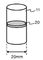
- FIG. 1A and FIG. 1B show an example of collecting a plate-like sample 20 for measuring residual stress by X-ray diffraction measurement from a polycrystalline silicon rod 10 grown by chemical vapor deposition such as Siemens (No. 1). It is a figure for demonstrating 1), and is the sample collection example for measuring the residual stress component of rr direction and (theta) theta direction.
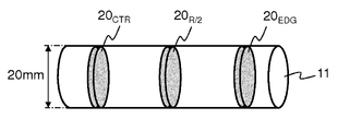
- FIGS. 2A and 2B are diagrams for explaining an example (second) of collecting the plate-like sample 20 for measuring residual stress by the X-ray diffraction measurement method, and these are also residuals in the rr direction and the ⁇ direction. It is a sample collection example for measuring a stress component. is there.
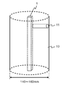
- 3A and 3B are diagrams for explaining an example (third) of collecting the plate-like sample 20 for residual stress measurement by the X-ray diffraction measurement method, for measuring the residual stress component in the zz direction. This is an example of sampling.
- reference numeral 1 denotes a silicon core wire for depositing polycrystalline silicon on the surface to form a silicon rod.
- the diameter of the polycrystalline silicon rod 10 illustrated in these drawings is approximately 140 to 160 mm, and a plate-like sample 20 for measuring residual stress is taken.
- part of the plate-shaped sample 20 is not limited to these.
- FIG. 1A when viewed in a plane perpendicular to the long axis direction, a portion close to the silicon core wire 1 (11 CTR ), a portion close to the side surface of the polycrystalline silicon rod 10 (11 EDG ), CTR A rod 11 having a diameter of approximately 20 mm is cut out from three portions (11 R / 2 ) in the middle of EGD and EGD. Then, as shown in FIG. 1B, a disk-shaped sample 20 having a thickness of approximately 2 mm is collected from the rod 11. The disc-shaped sample 20 taken from the rod 11 CTR 20 CTR, the rod 11 R / 2 the disc-shaped samples 20 taken from 20 R / 2, disc-shaped samples 20 taken from the rod 11 EDG 20 Indicated as EDG .
- a disk 12 centered on the silicon core wire 1 is sampled by slicing perpendicularly to the long axis direction. Then, as shown in FIG. 2B, the diameter of the circular plate 12 is approximately 20 mm from three parts, a part close to the silicon core wire 1, a part close to the side surface of the polycrystalline silicon rod 10, and an intermediate part between CTR and EGD.
- a disk-shaped sample (20 CTR , 20 R / 2 , 20 EDG ) is cut out.
- a disk-shaped sample taken from a cross section perpendicular to the major axis direction of the polycrystalline silicon rod 10 can be obtained.
- the X-ray irradiation region on the main surface of the disk-shaped sample with a slit By appropriately selecting the X-ray irradiation region on the main surface of the disk-shaped sample with a slit, the residual stress in the growth direction (rr) and the 90 degree direction ( ⁇ ) with respect to this direction is measured. be able to.
- a rod 11 having a diameter of approximately 20 mm is cut out perpendicularly to the long axis direction.
- the diameter of the rod 11 is approximately 20 mm from three parts, a part close to the silicon core wire 1, a part close to the side surface of the polycrystalline silicon rod 10, and an intermediate part between CTR and EGD.
- a disk-shaped sample (20 CTR , 20 R / 2 , 20 EDG ) is collected.
- a disk-shaped sample collected from a cross section parallel to the major axis direction of the polycrystalline silicon rod 10 is obtained.
- the residual stress in the major axis direction (zz) can be measured by appropriately selecting the X-ray irradiation region on the main surface of the disk-shaped sample with a slit.
- the disk-shaped sample 20 may also be collected from any part of the hollowed rod 11, but is preferably at a position where the properties of the entire silicon rod 10 can be reasonably estimated.
- the diameter of the disk-shaped sample 20 is set to approximately 20 mm for illustration only, and the diameter may be appropriately determined within a range that does not hinder the residual stress measurement.
- the residual stress ( ⁇ ) is the slope of the least square approximation line ( ⁇ (2 ⁇ ) / ⁇ (sin 2 ⁇ )) of the points plotted in the 2 ⁇ -sin 2 ⁇ diagram obtained by X-ray diffraction. Can be evaluated.
- the Young's modulus E the value of Young's modulus of polycrystalline silicon, which is an actual measurement sample, should be adopted.
- the literature value of 171.8 GPa for the Young's modulus of the ⁇ 111> orientation of single crystal silicon is adopted. did.
- the cause of residual stress is the temperature difference that has been established so far, but from the viewpoint of crystal growth, the following reasons for the generation are the main reasons.
- a polycrystalline silicon rod was grown under various CVD conditions summarized in Table 2, and the residual stress was examined.
- the temperature was measured by attaching a peephole to the CVD reactor and installing a radiation thermometer there.
- a radiation thermometer a radiation thermometer manufactured by Chino Corporation, model number IR-CAQ was used.
- the measurement wavelength is 0.9 ⁇ m
- the detection element material is silicon.
- the measurement position is the center position of the height of the polycrystalline silicon rod, and the focus position gradually changes as it grows. Therefore, the measurement value was obtained after fine adjustment of the focus each time measurement was performed.
- ⁇ T the average temperature of the rod was calculated according to the method described in Patent Document 3 (Japanese Patent Laid-Open No. 2001-146499), and then the center temperature was calculated from the above surface temperature.
- T2 T1 and T3 ⁇ T2
- Example 7 T1> T2 and T2 ⁇ T3, and the temperature difference between the temperatures T1 ′ and T3 in the vicinity of the silicon core wire when polycrystalline silicon is deposited in the outermost surface region is ⁇ T.
- T1> T2 and T2 ⁇ T3 the temperature difference between the temperatures T1 ′ and T3 in the vicinity of the silicon core wire when polycrystalline silicon is deposited in the outermost surface region is ⁇ T.
- the present invention controls residual stress by appropriately controlling the temperature during the process, A polycrystalline silicon rod suitable for producing crystalline silicon is provided. According to the method of the present invention, it is not necessary to perform heat treatment or the like conventionally performed after growing a polycrystalline silicon rod.
Landscapes
- Chemical & Material Sciences (AREA)
- Organic Chemistry (AREA)
- Inorganic Chemistry (AREA)
- Silicon Compounds (AREA)
Abstract
多結晶シリコン棒を合成する際に、シリコン芯線の近傍領域、R/2領域、最表面領域における多結晶シリコンの析出温度をそれぞれT1、T2、T3としたときに、T2=T1かつT3=T2、または、T2=T1かつT3<T2、または、T2>T1かつT3>T2、若しくは、T2>T1かつT3<T2となるように設定して多結晶シリコンを析出させる。T1>T2かつT2<T3とし、さらに、最表面領域における多結晶シリコンの析出時におけるシリコン芯線の近傍領域の温度T1´とT3との温度差をΔTとしたときに、T1<T3+ΔTとなるように設定してもよい。
Description
本発明は、多結晶シリコン棒の製造技術に関し、より具体的には、シーメンス法により合成される多結晶シリコン棒に残留する応力を制御し、CZ単結晶シリコンの製造用として好適な多結晶シリコン棒を製造する技術に関する。
半導体デバイス等の製造に不可欠な単結晶シリコン基板は、CZ法やFZ法により育成されたインゴットから切り出されるが、これらのインゴットの製造原料として、多結晶シリコン棒や多結晶シリコン塊が用いられる。
これらの多結晶シリコン原料は、一般に、シーメンス法により製造される。シーメンス法とは、トリクロロシランやモノシラン等のシラン原料ガスを加熱されたシリコン芯線に接触させることにより、該シリコン芯線の表面に多結晶シリコンをCVD(Chemical Vapor Deposition)法により気相成長(析出)させる方法である。
シリコン芯線の加熱は電流を流すことによる抵抗加熱によるが、多結晶シリコンの析出に伴い多結晶シリコン棒の径が太くなるにつれて、徐々に、シリコン棒の外表面には電流が流れ難くなる。その結果、外表面は中心領域の温度よりも相対的に低くなり、これが熱膨張率の差を引き起こし残留応力が発生する。このような残留応力の発生は、大口径の多結晶シリコン棒ほど顕著である。
ところで、残留応力には引張応力と圧縮応力があるが、前者は多結晶シリコンに割れを発生させるため強度低下を招く傾向があり、後者は、多結晶シリコンの強度を向上させる傾向がある。
従って、多結晶シリコン棒中の残留応力を制御することは極めて重要であり、これを破砕して多結晶シリコン塊とする際、引張応力の高いものは破砕が容易である一方、圧縮応力が高いものは破砕し難いこととなる。
多結晶シリコン棒中の圧縮応力が高く破砕し難い場合、破砕後のシリコン塊の粒径は揃い難く、目的とする範囲のサイズのものの収率が低くなってしまうなどの問題がある。
この様な事情を背景に、特許文献1(特許第3357675号明細書)には、デバイス等の製造に用いられるシリコン単結晶をリチャージ等により製造する際に、直接溶融炉に供給しても割れによるトラブルを防止し得る程度にまで残留歪みが低減され、しかも、安定した溶融特性を有する高純度の多結晶シリコンロッドおよびその製造方法に関する発明が開示されている。
また、特許文献2(特開2011-068558号公報)には、改善された破砕挙動を有する高純度シリコンからなる大きな直径(>100mm)を有する多結晶シリコンロッドを提供し、破砕に関連するシリコン破砕破片の汚染を大きく減らし、そして不所望な寸法を有するシリコン破砕破片の割合を減らすことを目的としたロッド状の多結晶シリコンに関する発明が開示されている。
S. Timoshenko and J.N. Goodier, "Theory of Elasticity ", McGraw-Hill, New York (1970)
Journal of the Ceramic Society of Japan 101[8]932-935 (1993)
CZ法で単結晶シリコンの育成をする際の原料は、シーメンス法で育成された多結晶シリコン棒を破砕して得られる多結晶シリコン塊である。上述のとおり、引張応力の高いものは破砕が容易である一方、圧縮応力が高いものは破砕し難いこととなるから、CZ単結晶シリコン育成用の原料に供される多結晶シリコン棒は、引張応力の高いものであることが好ましい。このような内部応力制御は、従来、育成後の多結晶シリコン棒を熱処理するなどの手法で対応してきた。しかし、多結晶シリコン棒の合成プロセスにおける残留応力制御の可能性についての検討はなされていない。
本発明は、斯かる現状に鑑みてなされたもので、その目的とするところは、多結晶シリコン棒の合成プロセス後ではなく、多結晶シリコン棒の合成プロセス中に残留応力制御を行い、合成後の多結晶シリコン棒の熱処理等を不要とする技術を提供することにある。
上記課題を解決するために、本発明に係る第1の態様の多結晶シリコン棒の製造方法は、シーメンス法によりシリコン芯線上に多結晶シリコンを析出させて得られる半径Rの多結晶シリコン棒の製造方法であって、前記シリコン芯線の近傍領域、R/2領域、最表面領域における多結晶シリコンの析出温度をそれぞれT1、T2、T3としたときに、T2=T1かつT3=T2に設定することを特徴とする。
また、本発明に係る第2の態様の多結晶シリコン棒の製造方法は、シーメンス法によりシリコン芯線上に多結晶シリコンを析出させて得られる半径Rの多結晶シリコン棒の製造方法であって、前記シリコン芯線の近傍領域、R/2領域、最表面領域における多結晶シリコンの析出温度をそれぞれT1、T2、T3としたときに、T2=T1かつT3<T2に設定することを特徴とする。
また、本発明に係る第3の態様の多結晶シリコン棒の製造方法は、シーメンス法によりシリコン芯線上に多結晶シリコンを析出させて得られる半径Rの多結晶シリコン棒の製造方法であって、前記シリコン芯線の近傍領域、R/2領域、最表面領域における多結晶シリコンの析出温度をそれぞれT1、T2、T3としたときに、T2>T1かつT3>T2に設定することを特徴とする。
また、本発明に係る第4の態様の多結晶シリコン棒の製造方法は、シーメンス法によりシリコン芯線上に多結晶シリコンを析出させて得られる半径Rの多結晶シリコン棒の製造方法であって、前記シリコン芯線の近傍領域、R/2領域、最表面領域における多結晶シリコンの析出温度をそれぞれT1、T2、T3としたときに、T2>T1かつT3<T2に設定することを特徴とする。
さらに、本発明に係る第5の態様の多結晶シリコン棒の製造方法は、シーメンス法によりシリコン芯線上に多結晶シリコンを析出させて得られる半径Rの多結晶シリコン棒の製造方法であって、前記シリコン芯線の近傍領域、R/2領域、最表面領域における多結晶シリコンの析出温度をそれぞれT1、T2、T3としたときに、T2<T1かつT3>T2とし、さらに、最表面領域における多結晶シリコンの析出時におけるシリコン芯線の近傍領域の温度T1´とT3との温度差をΔTとしたときに、T1<T3+ΔTとなるように設定することを特徴とする。
本発明は、シーメンス法によりシリコン芯線上に多結晶シリコンを析出させて半径Rの多結晶シリコン棒を得るプロセスにおいて、当該プロセス中の温度を適切に制御することにより残留応力を制御し、CZ単結晶シリコンの製造用として好適な多結晶シリコン棒を提供する。
本発明の方法によれば、従来は、多結晶シリコン棒育成後に行っていた熱処理等を行う必要がない。
以下に、図面を参照して、本発明に係る多結晶シリコン棒の製造方法について説明する。
従来より、場所による温度差が熱膨張α・T(温度)の差となり熱応力を発生させると言う考え方があり(例えば、非特許文献1:S. Timoshenko and J.N. Goodier, “Theory of Elasticity “, McGraw-Hill, New York (1970))、この考えに立った熱応力計算の方法も提案されている(非特許文献2:「円筒及び円板の熱応力計算法」, Journal of the Ceramic Society of Japan 101[8]932-935 (1993))。この計算方法は、一定太さの円筒の内部の温度分布を元に計算する手法であるが、シーメンス法による多結晶シリコン棒の析出のように徐々に径が太くなる場合には、応力計算することができない。加えて、この方法では、多結晶特有の構造に起因して発生する応力も考慮されていない。
そこで、本発明者らは、X線回折測定法(以下、XRD法)により結晶の面間隔値d値を精密測定することで、残留応力値を求める手法を検討した。この検討の結果、引張応力と圧縮応力はそれぞれが独立して結晶中に内在しており、単純な円筒内部の温度分布のみでは定まらないものであることが分かってきた。
本発明者らが、多結晶シリコン析出時のCVD温度と結晶中の残留応力の関係につき詳細に解析を重ねたところ、下記の規則性があることが判明した。
シーメンス法によりシリコン芯線上に多結晶シリコンを析出させて得られる多結晶シリコン棒の最終的な半径をRとし、シリコン芯線の近傍領域、R/2領域、最表面領域における多結晶シリコンの析出温度をそれぞれT1、T2、T3とし、さらに、最表面領域における多結晶シリコンの析出時におけるシリコン芯線の近傍領域の温度T1´とT3との温度差をΔTとすると、表1に纏めた関係が認められる。

ここで言う残留応力とは、多結晶シリコン棒の中心軸方向(鉛直方向:zz方向)の残留応力成分を意味している。残留応力の他の方向、すなわち、径方向(成長方向:rr方向)および当該rr方向と中心軸に垂直な平面内で90°の角度を成すθθ方向があるが、これらの残留応力成分は、本発明者らの検討によれば、結晶全体としての応力特性を代表するものではない。
結晶内に応力が生じていると、その大きさに比例して結晶格子の面間隔dは変化する。具体的には、引張応力が生じていると格子面間隔は広がり、圧縮応力が生じていると格子面間隔は縮まることになる。
ブラッグ回折を起こす結晶面に注目すると、その回折角θはブラッグ条件(nλ=2d・sinθ)を満足する。従って、X線の波長λが一定であれば、格子面間隔dの変化に伴って回折角2θも変化する。
結晶中の残留応力σは、X線回折で得られた2θ-sin2Ψ線図にプロットした点の最小2乗近似直線の傾き(Δ(2θ)/Δ(sin2Ψ))から、下記の式(1)で与えられる。
σ(MPa)=K・[Δ(2θ)/Δ(sin2Ψ)] ・・・ (1)
ここで、Ψは試料面法線と格子面法線とのなす角度(deg.)である。また、Kは応力定数(MPa/deg.)であり、下記の式(2)で与えられる。
K=-(E/2(1+ν))・cotθ0・π/180 ・・・ (2)
なお、式(2)中のEはヤング率(MPa)、νはポアソン比、そして、θ0は歪が無い状態でのブラッグ角(deg.)である。
つまり、X線回折法を用いれば、格子面法線を変化させながら特定の回折ピークの挙動を観測することで、格子面間隔の伸縮量から内部応力を求めることができる。
具体的には、内部応力がない場合には当然、回折ピークのシフトは生じないが、圧縮応力があると回折ピークは高角側へシフトし、引張応力があると回折ピークは低角側へシフトする。
本発明では、この原理に基づき、種々のCVD条件で合成した多結晶シリコンの残留応力を評価している。
[評価試料の採取]
図1Aおよび図1Bは、シーメンス法などの化学気相法で析出させて育成された多結晶シリコン棒10からの、X線回折測定法による残留応力測定用の板状試料20の採取例(第1)について説明するための図で、rr方向とθθ方向の残留応力成分を測定するための試料採取例である。
図1Aおよび図1Bは、シーメンス法などの化学気相法で析出させて育成された多結晶シリコン棒10からの、X線回折測定法による残留応力測定用の板状試料20の採取例(第1)について説明するための図で、rr方向とθθ方向の残留応力成分を測定するための試料採取例である。
また、図2Aおよび図2Bは、X線回折測定法による残留応力測定用の板状試料20の採取例(第2)について説明するための図で、これもまた、rr方向とθθ方向の残留応力成分を測定するための試料採取例である。
ある。
ある。
さらに、図3Aおよび図3Bは、X線回折測定法による残留応力測定用の板状試料20の採取例(第3)について説明するための図で、zz方向の残留応力成分を測定するための試料採取例である。
図中、符号1で示したものは、表面に多結晶シリコンを析出させてシリコン棒とするためのシリコン芯線である。これらの図に例示した多結晶シリコン棒10の直径は概ね140~160mmであり、残留応力測定用の板状試料20を採取する。なお、板状試料20の採取部位は、これらに限定されるものではない。
図1Aに示した第1例では、長軸方向に垂直な平面内でみたときに、シリコン芯線1に近い部位(11CTR)、多結晶シリコン棒10の側面に近い部位(11EDG)、CTRとEGDの中間の部位(11R/2)の3部位から、直径が概ね20mmのロッド11をくり抜く。そして、図1Bに示したように、このロッド11から、厚みが概ね2mmの円板状試料20を採取する。ロッド11CTRから採取された円板状試料20を20CTR、ロッド11R/2から採取された円板状試料20を20R/2、ロッド11EDGから採取された円板状試料20を20EDGと表記する。
これにより、多結晶シリコン棒10の長軸方向に垂直な断面から採取した円板状試料が得られる。この円板状試料の主面上でのX線照射領域をスリットで適切に選択することで、成長方向(rr)と、この方向に対して90度方向(θθ)の、残留応力を測定することができる。
図2Aに示した第2例では、先ず、長軸方向に垂直にスライスして、シリコン芯線1を中心とする円板12を採取する。そして、図2Bに示すように、この円板12の、シリコン芯線1に近い部位、多結晶シリコン棒10の側面に近い部位、CTRとEGDの中間の部位の3部位から、直径が概ね20mmの円板状試料(20CTR、20R/2、20EDG)をくり抜く。
これによっても、多結晶シリコン棒10の長軸方向に垂直な断面から採取した円板状試料が得られる。この円板状試料の主面上でのX線照射領域をスリットで適切に選択することで、成長方向(rr)と、この方向に対して90度方向(θθ)の、残留応力を測定することができる。
図3Aに示した第3例では、先ず、長軸方向に垂直に、直径が概ね20mmのロッド11をくり抜く。そして、図3Bに示したように、このロッド11から、シリコン芯線1に近い部位、多結晶シリコン棒10の側面に近い部位、CTRとEGDの中間の部位の3部位から、直径が概ね20mmの円板状試料(20CTR、20R/2、20EDG)を採取する。
これにより、多結晶シリコン棒10の長軸方向に平行な断面から採取した円板状試料が得られる。この円板状試料の主面上でのX線照射領域をスリットで適切に選択することで、長軸方向(zz)の残留応力を測定することができる。
なお、ロッド11を採取する部位、長さ、および本数は、シリコン棒10の直径やくり抜くロッド11の直径に応じて適宜定めればよい。円板状試料20も、くり抜いたロッド11のどの部位から採取してもよいが、シリコン棒10全体の性状を合理的に推定可能な位置であることが好ましい。
また、円板状試料20の直径を概ね20mmとしたのも例示に過ぎず、直径は残留応力測定に支障がない範囲で適当に定めればよい。
[X線回折法による応力測定]
上述のrr方向、θθ方向、およびzz方向の3方向での残留応力を測定すべく、直径19mmで厚さ2mmの円板状試料を採取する。採取した円板状試料を、ミラー指数面<331>からのブラッグ反射が検出される位置に配置し、X線照射領域が上述の3方向となるようにスリットを設定して、残留応力を測定する。なお、rr方向とθθ方向の2方向については、走査軸を平行にした並傾法と走査軸を直交する側傾法にて測定を行う。
上述のrr方向、θθ方向、およびzz方向の3方向での残留応力を測定すべく、直径19mmで厚さ2mmの円板状試料を採取する。採取した円板状試料を、ミラー指数面<331>からのブラッグ反射が検出される位置に配置し、X線照射領域が上述の3方向となるようにスリットを設定して、残留応力を測定する。なお、rr方向とθθ方向の2方向については、走査軸を平行にした並傾法と走査軸を直交する側傾法にて測定を行う。
上述のとおり、残留応力(σ)は、X線回折で得られた2θ-sin2Ψ線図にプロットした点の最小2乗近似直線の傾き(Δ(2θ)/Δ(sin2Ψ))で評価できる。
本来、ヤング率Eについては、実測定試料である多結晶シリコンのヤング率の値を採用すべきである。しかし、全結晶方位についての存在割合を考慮した上でのヤング率を算出することができないこと等の理由により、単結晶シリコンの<111>方位のヤング率の文献値である171.8GPaを採用した。
[残留応力のCVD条件依存性]
シーメンス法にて各種条件にて合成した、(a)炉内にて既に割れてしまったロッド、(b)ハンマーによる破砕テストにおいて割れ易かったロッド、および(c)ハンマーによる破砕テストにおいて割れ難かったロッドの三者について、XRD法による残留応力測定の結果を検討したところ、残留応力のzz方向成分に違いが認められた。
シーメンス法にて各種条件にて合成した、(a)炉内にて既に割れてしまったロッド、(b)ハンマーによる破砕テストにおいて割れ易かったロッド、および(c)ハンマーによる破砕テストにおいて割れ難かったロッドの三者について、XRD法による残留応力測定の結果を検討したところ、残留応力のzz方向成分に違いが認められた。
(a)炉内にて既に割れてしまったロッド、および(b)ハンマーによる破砕テストにおいて割れ易かったロッドのものにおいては、引張応力と圧縮応力の双方において高い値が認められたのに対し、(c)ハンマーによる破砕テストにおいて割れ難かったロッドのものにおいては、引張応力の値が低い一方で圧縮応力の値が高く、圧縮応力が優勢であることが判明した。
残留応力発生の原因が温度差であることはこれまでの定説であるが、結晶成長の観点から考えると以下の成長経緯による発生理由が有力である。
CVD反応の初期においてはシリコン芯線近傍において結晶析出が始まるが、この段階では結晶方位毎にランダムに結晶成長が進行し、やがて多結晶体を形成し始める。この時、この集合体としての全体の応力は結晶方位毎の各分力の合成、即ち、ベクトルの合成により定まる方向性を持った応力値が形成される。
さらに反応が進行すると、徐々に中心近傍領域と外側領域で温度差が発生する。この時の中心近傍領域温度(T1’)が、当該領域における結晶析出時の温度(T1)よりも低ければ(T1’<T1)当該領域の結晶中の応力は変わらないが、高い場合(T1’>T1)は結晶の再配列若しくは配向が起こり応力は変化する。
zz方向の残留応力に着目し、シリコン芯線の近傍領域、R/2領域、最表面領域(R領域)における残留応力を平均化した場合に、この平均値が(+)値の場合は引張応力を意味し、(-)値の場合は圧縮応力を意味する。
その結果、表1に示したとおりの分類が可能であることが判明した。
表2に纏めて示した各種CVD条件で多結晶シリコン棒を育成して、残留応力を調べた。
なお、温度測定は、CVD反応炉に覗き穴を取り付け、そこに放射温度計を設置し使用した。放射温度計は、株式会社チノー製の放射温度計、型番IR-CAQを使用した。測定波長は0.9μm、検出素子素材はシリコンである。測定位置は、多結晶シリコン棒の高さの中心位置であり、成長するに連れて焦点位置が徐々に変化するため測定の都度、焦点の微調整を行ってから測定値を得た。なお、ΔTの算出は、特許文献3(特開2001-146499号公報)に記載の方法に従い、ロッドの平均温度を算出後、上記の表面温度から中心温度を算出した。
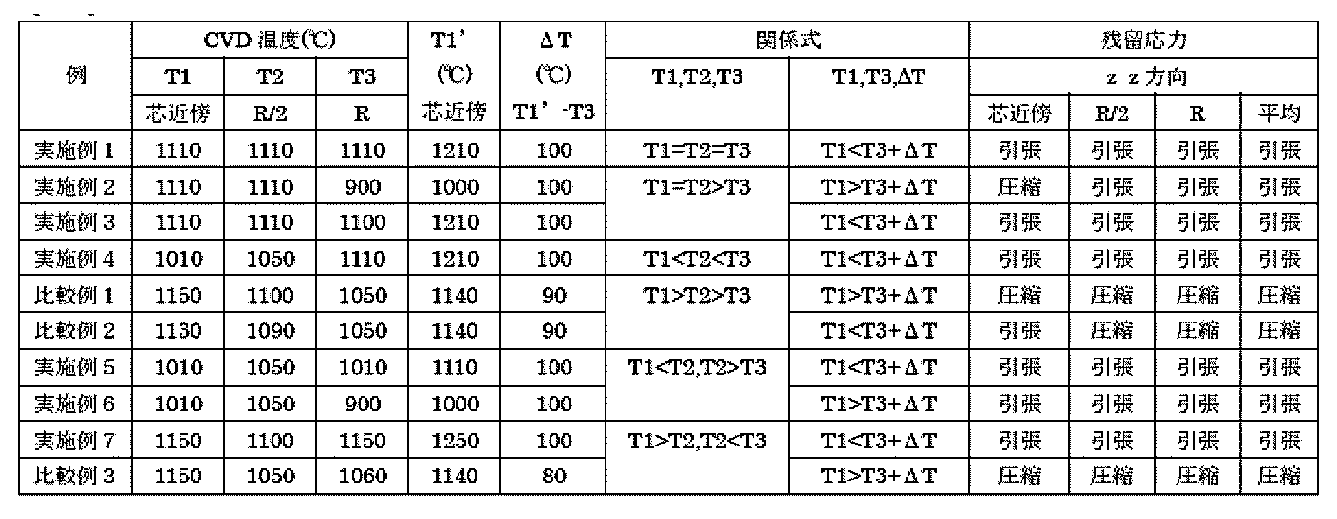
比較例1および比較例2のものは、シリコン芯線の近傍領域、R/2領域、最表面領域における多結晶シリコンの析出温度をそれぞれT1、T2、T3としたときに、T1>T2>T3に設定されて得られた多結晶シリコン棒であり、圧縮応力が優勢であって、破砕し難い多結晶シリコン棒であった。
また、比較例3のものは、シリコン芯線の近傍領域、R/2領域、最表面領域における多結晶シリコンの析出温度をそれぞれT1、T2、T3としたときに、T1>T2かつT2<T3とし、さらに、最表面領域における多結晶シリコンの析出時におけるシリコン芯線の近傍領域の温度T1´とT3との温度差をΔTとしたときに、T1>T3+ΔTとなるように設定されて得られた多結晶シリコン棒であり、これもまた圧縮応力が優勢であって、破砕し難い多結晶シリコン棒であった。
これに対し、実施例1~6のものは、T2=T1かつT3=T2、または、T2=T1かつT3<T2、または、T2>T1かつT3>T2、若しくは、T2>T1かつT3<T2に設定されて得られた多結晶シリコン棒であり、引張応力が優勢であって、破砕し易い多結晶シリコン棒であった。
また、実施例7のものは、T1>T2かつT2<T3とし、さらに、最表面領域における多結晶シリコンの析出時におけるシリコン芯線の近傍領域の温度T1´とT3との温度差をΔTとしたときに、T1<T3+ΔTとなるように設定されて得られた多結晶シリコン棒であり、これもまた引張応力が優勢であって、破砕し易い多結晶シリコン棒であった。
実施例1~7で得られた多結晶シリコン棒を、析出工程後の熱処理を行うことなく破砕して多結晶シリコン塊とし、これをCZ単結晶シリコン育成用の原料として用いたところ、結晶線の消失や乱れの発生もなく、良質なCZ単結晶シリコンのインゴットが得られた。
本発明は、シーメンス法によりシリコン芯線上に多結晶シリコンを析出させて半径Rの多結晶シリコン棒を得るプロセスにおいて、当該プロセス中の温度を適切に制御することにより残留応力を制御し、CZ単結晶シリコンの製造用として好適な多結晶シリコン棒を提供する。本発明の方法によれば、従来は、多結晶シリコン棒育成後に行っていた熱処理等を行う必要がない。
1 シリコン芯線
10 多結晶シリコン棒
11 ロッド
12 円板
20 円板状試料
10 多結晶シリコン棒
11 ロッド
12 円板
20 円板状試料
Claims (5)
- シーメンス法によりシリコン芯線上に多結晶シリコンを析出させて得られる半径Rの多結晶シリコン棒の製造方法であって、
前記シリコン芯線の近傍領域、R/2領域、最表面領域における多結晶シリコンの析出温度をそれぞれT1、T2、T3としたときに、T2=T1かつT3=T2に設定する、多結晶シリコン棒の製造方法。 - シーメンス法によりシリコン芯線上に多結晶シリコンを析出させて得られる半径Rの多結晶シリコン棒の製造方法であって、
前記シリコン芯線の近傍領域、R/2領域、最表面領域における多結晶シリコンの析出温度をそれぞれT1、T2、T3としたときに、T2=T1かつT3<T2に設定する、多結晶シリコン棒の製造方法。 - シーメンス法によりシリコン芯線上に多結晶シリコンを析出させて得られる半径Rの多結晶シリコン棒の製造方法であって、
前記シリコン芯線の近傍領域、R/2領域、最表面領域における多結晶シリコンの析出温度をそれぞれT1、T2、T3としたときに、T2>T1かつT3>T2に設定する、多結晶シリコン棒の製造方法。 - シーメンス法によりシリコン芯線上に多結晶シリコンを析出させて得られる半径Rの多結晶シリコン棒の製造方法であって、
前記シリコン芯線の近傍領域、R/2領域、最表面領域における多結晶シリコンの析出温度をそれぞれT1、T2、T3としたときに、T2>T1かつT3<T2に設定する、多結晶シリコン棒の製造方法。 - シーメンス法によりシリコン芯線上に多結晶シリコンを析出させて得られる半径Rの多結晶シリコン棒の製造方法であって、
前記シリコン芯線の近傍領域、R/2領域、最表面領域における多結晶シリコンの析出温度をそれぞれT1、T2、T3としたときに、T2<T1かつT3>T2とし、さらに、最表面領域における多結晶シリコンの析出時におけるシリコン芯線の近傍領域の温度T1´とT3との温度差をΔTとしたときに、T1<T3+ΔTとなるように設定する、多結晶シリコン棒の製造方法。
Applications Claiming Priority (2)
| Application Number | Priority Date | Filing Date | Title |
|---|---|---|---|
| JP2015174741A JP6378147B2 (ja) | 2015-09-04 | 2015-09-04 | 多結晶シリコン棒の製造方法およびcz単結晶シリコンの製造方法 |
| JP2015-174741 | 2015-09-04 |
Publications (1)
| Publication Number | Publication Date |
|---|---|
| WO2017038348A1 true WO2017038348A1 (ja) | 2017-03-09 |
Family
ID=58187251
Family Applications (1)
| Application Number | Title | Priority Date | Filing Date |
|---|---|---|---|
| PCT/JP2016/072593 Ceased WO2017038348A1 (ja) | 2015-09-04 | 2016-08-02 | 多結晶シリコン棒の製造方法およびcz単結晶シリコンの製造方法 |
Country Status (2)
| Country | Link |
|---|---|
| JP (1) | JP6378147B2 (ja) |
| WO (1) | WO2017038348A1 (ja) |
Families Citing this family (1)
| Publication number | Priority date | Publication date | Assignee | Title |
|---|---|---|---|---|
| JP7128124B2 (ja) * | 2019-01-18 | 2022-08-30 | 信越化学工業株式会社 | 多結晶シリコン棒、多結晶シリコンロッドおよびその製造方法 |
Citations (5)
| Publication number | Priority date | Publication date | Assignee | Title |
|---|---|---|---|---|
| JPS6374909A (ja) * | 1986-09-19 | 1988-04-05 | Shin Etsu Handotai Co Ltd | 大直径多結晶シリコン棒の製造方法 |
| JPH1143317A (ja) * | 1997-05-26 | 1999-02-16 | Tokuyama Corp | 表面状態の改善された多結晶シリコンロッド |
| JP2011037699A (ja) * | 2009-07-15 | 2011-02-24 | Mitsubishi Materials Corp | 多結晶シリコンの製造方法、製造装置及び多結晶シリコン |
| WO2013080556A1 (ja) * | 2011-11-29 | 2013-06-06 | 信越化学工業株式会社 | 多結晶シリコンの製造方法および多結晶シリコン製造用反応炉 |
| JP2015105917A (ja) * | 2013-12-02 | 2015-06-08 | 信越化学工業株式会社 | 多結晶シリコン棒の表面温度測定方法および多結晶シリコンの製造方法 |
-
2015
- 2015-09-04 JP JP2015174741A patent/JP6378147B2/ja active Active
-
2016
- 2016-08-02 WO PCT/JP2016/072593 patent/WO2017038348A1/ja not_active Ceased
Patent Citations (5)
| Publication number | Priority date | Publication date | Assignee | Title |
|---|---|---|---|---|
| JPS6374909A (ja) * | 1986-09-19 | 1988-04-05 | Shin Etsu Handotai Co Ltd | 大直径多結晶シリコン棒の製造方法 |
| JPH1143317A (ja) * | 1997-05-26 | 1999-02-16 | Tokuyama Corp | 表面状態の改善された多結晶シリコンロッド |
| JP2011037699A (ja) * | 2009-07-15 | 2011-02-24 | Mitsubishi Materials Corp | 多結晶シリコンの製造方法、製造装置及び多結晶シリコン |
| WO2013080556A1 (ja) * | 2011-11-29 | 2013-06-06 | 信越化学工業株式会社 | 多結晶シリコンの製造方法および多結晶シリコン製造用反応炉 |
| JP2015105917A (ja) * | 2013-12-02 | 2015-06-08 | 信越化学工業株式会社 | 多結晶シリコン棒の表面温度測定方法および多結晶シリコンの製造方法 |
Also Published As
| Publication number | Publication date |
|---|---|
| JP2017048099A (ja) | 2017-03-09 |
| JP6378147B2 (ja) | 2018-08-22 |
Similar Documents
| Publication | Publication Date | Title |
|---|---|---|
| JP6418778B2 (ja) | 多結晶シリコン棒、多結晶シリコン棒の製造方法、および、単結晶シリコン | |
| CN107848808B (zh) | 多晶硅棒 | |
| WO2013150758A1 (ja) | 多結晶シリコンの結晶配向度評価方法、多結晶シリコン棒の選択方法、および単結晶シリコンの製造方法 | |
| JP6131218B2 (ja) | 多結晶シリコン棒の表面温度の算出方法および制御方法、多結晶シリコン棒の製造方法、多結晶シリコン棒、ならびに、多結晶シリコン塊 | |
| CN107250038B (zh) | 多晶硅棒及其制造方法和fz硅单晶 | |
| WO2013190829A1 (ja) | 多結晶シリコンの結晶配向度評価方法、多結晶シリコン棒の選択方法、多結晶シリコン棒、多結晶シリコン塊、および、単結晶シリコンの製造方法 | |
| JP2016041636A (ja) | 多結晶シリコン棒の製造方法および多結晶シリコン棒 | |
| JP6440601B2 (ja) | 多結晶シリコン棒の製造方法およびfz単結晶シリコンの製造方法 | |
| JP2016028990A (ja) | 多結晶シリコン棒の製造方法および多結晶シリコン塊 | |
| JP6378147B2 (ja) | 多結晶シリコン棒の製造方法およびcz単結晶シリコンの製造方法 | |
| JP5868286B2 (ja) | 多結晶シリコン棒の選択方法、多結晶シリコン塊の製造方法、及び、単結晶シリコンの製造方法 | |
| JP2022009646A (ja) | 多結晶シリコン棒および多結晶シリコン棒の製造方法 | |
| JP5969956B2 (ja) | 多結晶シリコンの粒径評価方法および多結晶シリコン棒の選択方法 | |
| US11167994B2 (en) | Polycrystalline silicon rod, processing method for polycrystalline silicon rod, method for evaluating polycrystalline silicon rod, and method for producing FZ single crystal silicon | |
| CN105358967A (zh) | 多晶硅的晶体粒径分布的评价方法 | |
| JP6470223B2 (ja) | 単結晶シリコンの製造方法 |
Legal Events
| Date | Code | Title | Description |
|---|---|---|---|
| 121 | Ep: the epo has been informed by wipo that ep was designated in this application |
Ref document number: 16841380 Country of ref document: EP Kind code of ref document: A1 |
|
| NENP | Non-entry into the national phase |
Ref country code: DE |
|
| 122 | Ep: pct application non-entry in european phase |
Ref document number: 16841380 Country of ref document: EP Kind code of ref document: A1 |