WO2017033828A1 - 有機半導体素子用インク組成物およびこれを用いた有機半導体素子 - Google Patents
有機半導体素子用インク組成物およびこれを用いた有機半導体素子 Download PDFInfo
- Publication number
- WO2017033828A1 WO2017033828A1 PCT/JP2016/074095 JP2016074095W WO2017033828A1 WO 2017033828 A1 WO2017033828 A1 WO 2017033828A1 JP 2016074095 W JP2016074095 W JP 2016074095W WO 2017033828 A1 WO2017033828 A1 WO 2017033828A1
- Authority
- WO
- WIPO (PCT)
- Prior art keywords
- solvent
- layer
- ink composition
- organic semiconductor
- leveling agent
- Prior art date
- Legal status (The legal status is an assumption and is not a legal conclusion. Google has not performed a legal analysis and makes no representation as to the accuracy of the status listed.)
- Ceased
Links
Classifications
-
- H—ELECTRICITY
- H10—SEMICONDUCTOR DEVICES; ELECTRIC SOLID-STATE DEVICES NOT OTHERWISE PROVIDED FOR
- H10K—ORGANIC ELECTRIC SOLID-STATE DEVICES
- H10K85/00—Organic materials used in the body or electrodes of devices covered by this subclass
- H10K85/10—Organic polymers or oligomers
- H10K85/151—Copolymers
-
- C—CHEMISTRY; METALLURGY
- C09—DYES; PAINTS; POLISHES; NATURAL RESINS; ADHESIVES; COMPOSITIONS NOT OTHERWISE PROVIDED FOR; APPLICATIONS OF MATERIALS NOT OTHERWISE PROVIDED FOR
- C09D—COATING COMPOSITIONS, e.g. PAINTS, VARNISHES OR LACQUERS; FILLING PASTES; CHEMICAL PAINT OR INK REMOVERS; INKS; CORRECTING FLUIDS; WOODSTAINS; PASTES OR SOLIDS FOR COLOURING OR PRINTING; USE OF MATERIALS THEREFOR
- C09D11/00—Inks
- C09D11/02—Printing inks
- C09D11/03—Printing inks characterised by features other than the chemical nature of the binder
-
- C—CHEMISTRY; METALLURGY
- C09—DYES; PAINTS; POLISHES; NATURAL RESINS; ADHESIVES; COMPOSITIONS NOT OTHERWISE PROVIDED FOR; APPLICATIONS OF MATERIALS NOT OTHERWISE PROVIDED FOR
- C09D—COATING COMPOSITIONS, e.g. PAINTS, VARNISHES OR LACQUERS; FILLING PASTES; CHEMICAL PAINT OR INK REMOVERS; INKS; CORRECTING FLUIDS; WOODSTAINS; PASTES OR SOLIDS FOR COLOURING OR PRINTING; USE OF MATERIALS THEREFOR
- C09D11/00—Inks
- C09D11/02—Printing inks
- C09D11/10—Printing inks based on artificial resins
- C09D11/102—Printing inks based on artificial resins containing macromolecular compounds obtained by reactions other than those only involving unsaturated carbon-to-carbon bonds
-
- C—CHEMISTRY; METALLURGY
- C09—DYES; PAINTS; POLISHES; NATURAL RESINS; ADHESIVES; COMPOSITIONS NOT OTHERWISE PROVIDED FOR; APPLICATIONS OF MATERIALS NOT OTHERWISE PROVIDED FOR
- C09D—COATING COMPOSITIONS, e.g. PAINTS, VARNISHES OR LACQUERS; FILLING PASTES; CHEMICAL PAINT OR INK REMOVERS; INKS; CORRECTING FLUIDS; WOODSTAINS; PASTES OR SOLIDS FOR COLOURING OR PRINTING; USE OF MATERIALS THEREFOR
- C09D11/00—Inks
- C09D11/30—Inkjet printing inks
-
- C—CHEMISTRY; METALLURGY
- C09—DYES; PAINTS; POLISHES; NATURAL RESINS; ADHESIVES; COMPOSITIONS NOT OTHERWISE PROVIDED FOR; APPLICATIONS OF MATERIALS NOT OTHERWISE PROVIDED FOR
- C09D—COATING COMPOSITIONS, e.g. PAINTS, VARNISHES OR LACQUERS; FILLING PASTES; CHEMICAL PAINT OR INK REMOVERS; INKS; CORRECTING FLUIDS; WOODSTAINS; PASTES OR SOLIDS FOR COLOURING OR PRINTING; USE OF MATERIALS THEREFOR
- C09D11/00—Inks
- C09D11/52—Electrically conductive inks
-
- H—ELECTRICITY
- H05—ELECTRIC TECHNIQUES NOT OTHERWISE PROVIDED FOR
- H05B—ELECTRIC HEATING; ELECTRIC LIGHT SOURCES NOT OTHERWISE PROVIDED FOR; CIRCUIT ARRANGEMENTS FOR ELECTRIC LIGHT SOURCES, IN GENERAL
- H05B33/00—Electroluminescent light sources
- H05B33/12—Light sources with substantially two-dimensional [2D] radiating surfaces
- H05B33/20—Light sources with substantially two-dimensional [2D] radiating surfaces characterised by the chemical or physical composition or the arrangement of the material in which the electroluminescent material is embedded
-
- H—ELECTRICITY
- H10—SEMICONDUCTOR DEVICES; ELECTRIC SOLID-STATE DEVICES NOT OTHERWISE PROVIDED FOR
- H10K—ORGANIC ELECTRIC SOLID-STATE DEVICES
- H10K10/00—Organic devices specially adapted for rectifying, amplifying, oscillating or switching; Organic capacitors or resistors having potential barriers
-
- H—ELECTRICITY
- H10—SEMICONDUCTOR DEVICES; ELECTRIC SOLID-STATE DEVICES NOT OTHERWISE PROVIDED FOR
- H10K—ORGANIC ELECTRIC SOLID-STATE DEVICES
- H10K50/00—Organic light-emitting devices
- H10K50/10—OLEDs or polymer light-emitting diodes [PLED]
- H10K50/14—Carrier transporting layers
-
- H—ELECTRICITY
- H10—SEMICONDUCTOR DEVICES; ELECTRIC SOLID-STATE DEVICES NOT OTHERWISE PROVIDED FOR
- H10K—ORGANIC ELECTRIC SOLID-STATE DEVICES
- H10K50/00—Organic light-emitting devices
- H10K50/10—OLEDs or polymer light-emitting diodes [PLED]
- H10K50/14—Carrier transporting layers
- H10K50/15—Hole transporting layers
-
- H—ELECTRICITY
- H10—SEMICONDUCTOR DEVICES; ELECTRIC SOLID-STATE DEVICES NOT OTHERWISE PROVIDED FOR
- H10K—ORGANIC ELECTRIC SOLID-STATE DEVICES
- H10K71/00—Manufacture or treatment specially adapted for the organic devices covered by this subclass
- H10K71/10—Deposition of organic active material
- H10K71/12—Deposition of organic active material using liquid deposition, e.g. spin coating
- H10K71/13—Deposition of organic active material using liquid deposition, e.g. spin coating using printing techniques, e.g. ink-jet printing or screen printing
- H10K71/135—Deposition of organic active material using liquid deposition, e.g. spin coating using printing techniques, e.g. ink-jet printing or screen printing using ink-jet printing
-
- H—ELECTRICITY
- H10—SEMICONDUCTOR DEVICES; ELECTRIC SOLID-STATE DEVICES NOT OTHERWISE PROVIDED FOR
- H10K—ORGANIC ELECTRIC SOLID-STATE DEVICES
- H10K71/00—Manufacture or treatment specially adapted for the organic devices covered by this subclass
- H10K71/10—Deposition of organic active material
- H10K71/12—Deposition of organic active material using liquid deposition, e.g. spin coating
- H10K71/15—Deposition of organic active material using liquid deposition, e.g. spin coating characterised by the solvent used
-
- H—ELECTRICITY
- H10—SEMICONDUCTOR DEVICES; ELECTRIC SOLID-STATE DEVICES NOT OTHERWISE PROVIDED FOR
- H10K—ORGANIC ELECTRIC SOLID-STATE DEVICES
- H10K85/00—Organic materials used in the body or electrodes of devices covered by this subclass
- H10K85/40—Organosilicon compounds, e.g. TIPS pentacene
Definitions
- the present invention relates to an ink composition for an organic semiconductor element and an organic semiconductor element using the same.
- the organic semiconductor element is an electroluminescent element using an organic compound (organic semiconductor) having semiconductor properties. Since organic semiconductor elements use organic semiconductors, they can be reduced in weight, increased in area, made flexible, and so on, and research and development in this field has been promoted rapidly in recent years. Of organic semiconductor elements, organic light-emitting elements, organic field effect transistors, and organic solar cells are particularly attracting attention.
- organic light-emitting elements are attracting attention as next-generation flat panel displays, next-generation lighting, and the like from the viewpoints of excellent visibility, low viewing angle dependency, and possible thinning.
- Organic light emitting elements usually include an anode, a hole transport layer, a light emitting layer, an electron transport layer, and a cathode.
- a voltage is applied to the organic light emitting device, holes are injected from the anode into the hole transport layer, electrons are injected from the cathode into the electron transport layer, and then holes and electrons are injected into the light emitting layer.
- the injected holes and electrons are recombined, and the light emitting material in the light emitting layer emits light by the energy generated at this time.
- the organic light emitting device does not have a hole transport layer and / or an electron transport layer.
- other layers such as a positive hole injection layer and an electron injection layer, may be included.
- an organic semiconductor element is applied with a coating liquid (ink composition) containing an organic material instead of a dry film formation in which a film is formed by vapor deposition of an organic material from the viewpoint of increasing the size and cost of the element.
- the current density greatly depends on the film thickness, and the portion where the film thickness is thin induces leakage current.
- Flatness is required for a layer constituting the light emitting element.
- organic field effect transistors and solar cells are required to have flatness in the constituent layers in order to suppress leakage current.
- Patent Document 1 describes an invention related to a coating liquid for forming an organic EL layer used when forming an organic layer of an organic EL element.
- the coating liquid for forming the organic EL layer includes a leveling agent and a light emitting material or a charge transporting material, and the addition amount of the leveling agent (L) is L viscosity (cp) ⁇ light emission. The amount of L added to the material or charge transport material (wt%) ⁇ 200 is satisfied.
- Patent Document 1 discloses that a specific amount of a leveling agent is included in the coating liquid for forming an organic EL layer to solve problems such as light emission unevenness caused by flatness of a film formed by a wet film forming method. It states that it can be done.
- a layer formed by a wet film forming method can have a certain flatness. More specifically, by causing the leveling agent to be oriented on the surface of the coating film formed by coating, the occurrence of waviness can be prevented and flatness can be realized.
- the leveling agent is oriented on the surface portion of the layer formed from the coating film having the leveling agent oriented on the surface. Then, the surface of such a layer has a small surface energy due to the presence of the leveling agent, and as a result, the layer formed by using the leveling agent cannot be formed by a wet film formation method. Or it turned out to be very difficult.
- an object of the present invention is to provide an ink composition for an organic semiconductor element capable of forming a suitable film even on a low surface energy layer.
- the present inventors have conducted intensive research to solve the above problems. As a result, the inventors have found that the above problem can be solved by using a predetermined leveling agent and a predetermined solvent in the ink composition for organic semiconductor elements, and have completed the present invention.
- the present invention includes a first organic semiconductor element material, a leveling agent, a first solvent, and an aromatic solvent, and the leveling agent is a polymer containing at least a siloxane monomer as a monomer unit, It is related with the ink composition for organic semiconductor elements whose surface tension of a 1st solvent is 25 mN / m or less.
- a film can be suitably formed even on a low surface energy layer.
- the ink composition for an organic semiconductor element includes a first organic semiconductor element material, a leveling agent, a first solvent, and an aromatic solvent.
- the leveling agent is a polymer containing at least a siloxane monomer as a monomer unit. Further, the surface tension of the first solvent is 25 mN / m or less.
- the layer formed using the organic semiconductor element ink composition containing the leveling agent has a low surface energy because the leveling agent is oriented on the surface of the layer. If an ink composition for organic semiconductor elements is further formed on such a low surface energy layer by a wet film formation method, a coating film is difficult to form or cannot be formed. Specifically, when the ink composition for an organic semiconductor element is applied, the contact angle becomes remarkably large, and sufficient wettability cannot be ensured.
- the organic semiconductor element is an organic light emitting element
- the low surface energy layer is a hole injection layer
- the layer to be formed is a hole transport layer. If the hole transport layer is formed by the ink composition, the wettability is not sufficient.
- the coating film itself cannot be formed, and even if the coating film can be formed, undulation is generated on the surface of the hole transport layer obtained by drying.
- the adhesion between the hole transport layer—the hole injection layer and / or the hole transport layer—the light emitting layer (formed on the hole transport layer) is lowered, and the performance of the organic light emitting device is lowered. sell.
- the organic semiconductor element material may be difficult to dissolve or may not be dissolved.
- the application range of the ink composition for a semiconductor element is remarkably narrow or cannot be applied.
- the ink composition for organic semiconductor elements according to the present embodiment can form a film suitably even on the low surface energy layer.
- the reason for this is not necessarily clear, but is thought to be due to the following mechanism. That is, when the ink composition for organic semiconductor elements contains the first solvent having a surface tension of 25 mN / m or less, the wettability of the ink composition for organic semiconductor elements is improved, and even on the low surface energy layer. It becomes possible to apply suitably. Moreover, since the ink composition for organic semiconductor elements further contains an aromatic solvent excellent in solubility of the organic semiconductor element material, the organic semiconductor element material can be suitably dissolved. That is, by using the first solvent and the aromatic solvent in combination as the solvent, both wettability and solubility of the organic semiconductor element material can be achieved.
- the leveling agent is a polymer containing at least a siloxane monomer as a monomer unit, layer formation on the low surface energy layer can be made more reliable.
- the first solvent having a small surface energy is relatively easier to evaporate than the aromatic solvent.
- the 1st solvent may preferentially evaporate from a coating film.
- the leveling agent has a siloxane structure, it is easily oriented on the surface of the coating film, and the evaporation rate of the first solvent and the aromatic solvent can be controlled. More specifically, the leveling agent oriented on the surface of the coating film can suppress or prevent preferential evaporation of the first solvent. Thereby, in the drying process of a coating film, a 1st solvent and an aromatic solvent will evaporate to the same extent, and the layer formed may be excellent in flatness. Note that the action mechanism of the leveling agent is speculative, and even if the effect of the invention is obtained by a mechanism different from the above mechanism, it is included in the technical scope of the present invention.
- the ink composition for organic light-emitting elements will be described in detail as an example of the ink composition for organic semiconductor elements.
- those skilled in the art can use materials used for organic field effect transistors and organic solar cells.
- An ink composition for organic field effect transistors and an ink composition for organic solar cells can be obtained.
- those skilled in the art will understand that the effects of the present invention can also be obtained with the obtained ink composition for organic field effect transistors and the ink composition for organic solar cells.
- the first semiconductor element material is a first organic light emitting element material.
- the first organic light emitting device material is not particularly limited, and any material can be used as long as it is a material constituting the organic light emitting device.
- the ink composition for an organic light emitting device is preferably applied on a low surface energy layer formed by a wet film forming method.
- the low surface energy layer include a hole injection layer and a hole transport layer.
- the layer that can be formed on the hole injection layer include a hole transport layer and a light emitting layer.
- a light emitting layer is mentioned as a layer which can be formed on the said positive hole transport layer.
- the first organic light emitting device material is preferably a hole transport material used for the hole transport layer and a light emitting material used for the light emitting layer.
- the hole transport material has a function of efficiently transporting holes in the hole transport layer.
- the holes are usually transported from the hole transport material to the light emitting layer.
- the hole transport material is not particularly limited, but TPD (N, N′-diphenyl-N, N′-di (3-methylphenyl) -1,1′-biphenyl-4,4′diamine (the following chemical formula HTM03 )), ⁇ -NPD (4,4′-bis [N- (1-naphthyl) -N-phenylamino] biphenyl), m-MTDATA (4,4 ′, 4 ′′ -tris (3-methylphenylphenylamino) ) Triphenylamine derivatives such as triphenylamine); polyvinylcarbazole; polymerization by introducing substituents into triphenylamine derivatives represented by the following chemical formulas HTM01 and HTM02 (n is an integer of 1 to 10,000) Among these, the hole transport material is a triphenylamine derivative from the viewpoint of excellent solubility in an aromatic solvent. Is preferably a polymer compound obtained by polymerization by introducing a substituent group
- the above hole transport materials may be used alone or in combination of two or more.
- the content of the hole transport material is preferably 0.01 to 10% by mass and more preferably 0.01 to 5% by mass with respect to the total amount of the ink composition for an organic light emitting device. It is preferable that the content of the hole transport material is 0.01% by mass or more because holes can be effectively transported. On the other hand, when the content of the hole transport material is 10% by mass or less, it is preferable because an increase in driving voltage can be suppressed.
- the light emitting material has a function of directly or indirectly contributing to light emission using holes and electrons in the light emitting layer.
- emission includes emission by fluorescence and emission by phosphorescence.
- the luminescent material includes a host material and a dopant material.
- the host material usually has a function of transporting holes and electrons injected into the light emitting layer.
- the host material is not particularly limited as long as it has the above functions. Host materials are classified into high molecular host materials and low molecular host materials.
- low molecule means that having a weight average molecular weight (Mw) of 5,000 or less.
- polymer means a polymer having a weight average molecular weight (Mw) of more than 5,000.
- the value of “weight average molecular weight (Mw)” is a value measured using polystyrene as a standard substance using a high-speed gel permeation chromatography (GPC) apparatus (manufactured by Tosoh Corporation). To do.
- GPC gel permeation chromatography
- the polymer host material is not particularly limited, and examples thereof include poly (9-vinylcarbazole) (PVK), polyfluorene (PF), polyphenylene vinylene (PPV), and copolymers containing these monomer units.
- PVK poly (9-vinylcarbazole)
- PF polyfluorene
- PPV polyphenylene vinylene
- the weight average molecular weight (Mw) of the polymer host material is preferably more than 5,000 and less than 5,000,000, and more preferably more than 5,000 and less than 1,000,000.
- the low molecular host material is not particularly limited, but 4,4′-bis (9H-carbazol-9-yl) biphenyl (CBP), bis (2-methyl-8-quinolinolate) -4- (phenylphenolate) Aluminum (BAlq), 1,3-dicarbazolylbenzene (mCP), 4,4′-bis (9-carbazolyl) -2,2′-dimethylbiphenyl (CDBP), N, N′-dicarbazolyl-1, 4-dimethylbenzene (DCB), 2,7-bis (diphenylphosphine oxide) -9,9-dimethylfluorescene (P06), 3,5-bis (9-carbazolyl) tetraphenylsilane (SimCP), 1, 3-bis (triphenylsilyl) benzene (UGH3), 1,3,5-tris [4- (diphenylamino) phenyl] benzene (T APB), 9,9 ′-(p-tert-
- the weight average molecular weight (Mw) of the low molecular weight host material is preferably 100 to 5,000, and more preferably 300 to 5,000.
- a low molecular weight host material is preferably used as the host material, and 4,4′-bis (9H-carbazol-9-yl) biphenyl (CBP), bis (2-methyl-8- Quinolinolate) -4- (phenylphenolato) aluminum (BAlq), 9,9 ′-(p-tert-butylphenyl) -1,3-biscarbazole (TBPBCz), 9- (4,6-diphenyl-1, More preferably, 3,5-triazin-2-yl) -9′-phenyl-3,3′-biscarbazole (CzT) is used, and 4,4′-bis (9H-carbazol-9-yl) biphenyl ( CBP), 9,9 ′-(p-tert-butylphenyl) -1,3-biscarbazole (TBPBCz), 9- (4,6-diphenyl-1,3,5- It is more preferable to use a triazine-2-yl)
- the above host materials may be used alone or in combination of two or more.
- the content of the host material is preferably 0.1 to 10% by mass, and more preferably 0.1 to 5% by mass with respect to the total amount of the ink composition for an organic light emitting device.
- the content of the host material is 0.1% by mass or more, it is preferable because the intermolecular distance between the host molecule and the dopant molecule can be shortened.
- the content of the host material is 10% by mass or less, it is preferable because a decrease in quantum yield can be suppressed.
- Dopant Material has a function of emitting light using energy obtained by recombining transported holes and electrons.
- the dopant material is not particularly limited as long as it has the above functions.
- the dopant material is usually classified into a high molecular dopant material and a low molecular dopant material.
- the polymer dopant material is not particularly limited, but polyphenylene vinylene (PPV), cyano polyphenylene vinylene (CN-PPV), poly (fluorenylene ethynylene) (PFE), polyfluorene (PFO), polythiophene polymer, polypyridine, And copolymers containing these monomer units.
- the weight average molecular weight (Mw) of the polymer dopant material is preferably more than 5,000 and less than 5,000,000, and more preferably more than 5,000 and less than 1,000,000.
- the low molecular dopant material is not particularly limited, and examples thereof include fluorescent materials and phosphorescent materials.
- fluorescent light-emitting material examples include naphthalene, perylene, pyrene, chrysene, anthracene, coumarin, p-bis (2-phenylethenyl) benzene, quinacridone, coumarin, aluminum complexes such as Al (C 9 H 6 NO) 3, etc.
- Examples of the phosphorescent material include a complex containing a central metal of Groups 7 to 11 of the periodic table and an aromatic ligand coordinated to the central metal.
- Examples of the central metal of Group 7 to Group 11 of the periodic table include ruthenium, rhodium, palladium, osmium, iridium, gold, platinum, silver, and copper. Of these, the central metal is preferably iridium or platinum.
- the ligand examples include phenylpyridine, diphenylpyridine, p-tolylpyridine, thienylpyridine, difluorophenylpyridine, phenylisoquinoline, fluorenopyridine, fluorenoquinoline, acetylacetone, and derivatives thereof.
- the ligand is preferably phenylpyridine, diphenylpyridine, p-tolylpyridine, and derivatives thereof, and more preferably p-tolylpyridine and derivatives thereof.
- Specific phosphorescent materials include tris (2-phenylpyridine) iridium (Ir (ppy) 3 ), tris (2-phenylpyridine) ruthenium, tris (2-phenylpyridine) palladium, bis (2-phenylpyridine) Platinum, tris (2-phenylpyridine) osmium, tris (2-phenylpyridine) rhenium, tris [2- (p-tolyl) pyridine] iridium (Ir (mppy) 3 ), tris [2- (p-tolyl) pyridine ] Ruthenium, tris [2- (p-tolyl) pyridine] palladium, tris [2- (p-tolyl) pyridine] platinum, tris [2- (p-tolyl) pyridine] osmium, tris [2- (p-tolyl) ) Pyridine] rhenium, octaethylplatinum porphyrin, octaphenyl
- the dopant material is preferably a low molecular dopant material, more preferably a phosphorescent material, and is tris [2- (p-tolyl) pyridine] iridium (Ir (mppy) 3 ). Is more preferable.
- the weight average molecular weight (Mw) of the low molecular dopant material is preferably 100 to 5,000, and more preferably 100 to 3,000.
- the above dopant materials may be used alone or in combination of two or more.
- the content of the dopant material is preferably 0.01 to 10% by mass and more preferably 0.01 to 5% by mass with respect to the total amount of the ink composition for an organic light emitting device.
- the content of the dopant material is 0.01% by mass or more, the emission intensity can be increased, which is preferable.
- the content of the dopant material is 10% by mass or less because a decrease in quantum yield can be suppressed.
- the light emitting material it is preferable to use a low molecular light emitting material, more preferably a low molecular host material and a low molecular dopant material, from the viewpoint that higher luminous efficiency can be obtained. More preferably, (p-tolyl) pyridine] iridium (Ir (mppy) 3 ) and 9,9 ′-(p-tert-butylphenyl) -1,3-biscarbazole are used.
- Leveling agent is oriented on the surface of the coating film formed using the ink composition for an organic light emitting device, and has a function of suppressing or preventing preferential evaporation of the first solvent when the coating film is dried.
- the leveling agent is oriented on the surface of the coating film formed using the ink composition for an organic light emitting device, and has a function of suppressing or preventing the undulation of the layer.
- the leveling agent according to this embodiment is a polymer containing at least a siloxane monomer as a monomer unit.
- the leveling agent may further contain an aromatic-containing monomer as a monomer unit.
- the hydrophobic monomer may be included as a monomer unit.
- the component resulting from a polymerization initiator may be included.
- siloxane monomer The siloxane monomer includes a siloxane group, a polymerizable functional group, and a first linking group. At this time, the first linking group connects the siloxane group and the polymerizable functional group.
- siloxane means a structure of “—Si—O—Si—” (siloxane structure).
- each R 1 is independently a hydrogen atom, a C1-C30 alkyl group, a C3-C30 cycloalkyl group, or a C1-C30 alkylsilyloxy group.
- the C1-C30 alkyl group is not particularly limited, and examples thereof include methyl, ethyl, propyl, isopropyl, butyl, iso-butyl, sec-butyl, tert-butyl, pentyl, hexyl, decyl, undecyl, octadecyl and the like.
- the C3-C30 cycloalkyl group is not particularly limited, and examples thereof include cyclopropyl, cyclobutyl, cyclopentyl, cyclohexyl, cycloheptyl, tricyclo [5,2,1,0 (2,6)] decyl, adamantyl and the like. It is done.
- the C1-C30 alkylsilyloxy group is not particularly limited, but includes methylsilyloxy, dimethylsilyloxy, trimethylsilyloxy, ethylsilyloxy, diethylsilyloxy, triethylsilyloxy, ethylmethylsilyloxy, diethylmethylsilyloxy, and the like. Can be mentioned.
- At this time, at least one of the hydrogen atoms constituting the C1 to C30 alkyl group, the C3 to C30 cycloalkyl group, and the C1 to C30 alkylsilyloxy group may be substituted with a substituent.
- substituents include halogen atom; hydroxy group; thiol group; nitro group; sulfo group; C1-C10 alkoxy group such as methoxy, ethoxy, propyl, isopropyloxy, butoxy; methylamino, ethylamino, dimethylamino, diethylamino, etc.
- a carbonyl group is mentioned.
- R 1 preferably contains a hydrogen atom, a C1-C30 alkyl group, a C1-C30 alkylsilyloxy group, and is a hydrogen atom, methyl, ethyl, propyl, isopropyl, butyl, iso-butyl, sec-butyl. , Tert-butyl, trimethylsilyloxy, and triethylsilyloxy are more preferable, and a hydrogen atom, methyl, ethyl, propyl, and trimethylsilyloxy are further preferable.
- N is 1 to 1000, preferably 1 to 200.
- the polymerizable functional group possessed by the siloxane monomer is not particularly limited, and examples thereof include acrylic, methacrylic, glycidyl, vinyl and vinylidene. Of these, the polymerizable functional group is preferably acrylic or methacrylic.
- examples of the first linking group possessed by the siloxane monomer include a single bond, an oxygen atom, a sulfur atom, and a C1-C10 alkylene group.
- the C1-C10 alkylene group is not particularly limited, but includes methylene, ethylene, propylene, isopropylene, butylene, iso-butylene, sec-butylene, pentylene, and the like.
- At this time, at least one of the hydrogen atoms constituting the C1-C10 alkylene group may be substituted with the above-described substituent.
- the first linking group is preferably a single bond or a C1-C10 alkylene group, and more preferably a single bond, methylene, ethylene or propylene.
- the above siloxane monomers may be used alone or in combination of two or more.
- the aromatic-containing monomer has a function of improving the affinity with the aromatic solvent. Thereby, a leveling agent can melt
- the aromatic-containing monomer includes an aromatic group, a polymerizable functional group, and a second linking group. At this time, the second linking group links the aromatic group and the polymerizable functional group.
- the aromatic group is not particularly limited, but is a C6-C30 aryl group.
- the C6 to C30 aryl group include phenyl, naphthyl, anthracenyl, biphenyl and the like.
- at least one hydrogen atom constituting the C6 to C30 aryl group may be substituted with a C1 to C30 alkyl group, a C3 to C30 cycloalkyl group, or the above-described substituent.
- the polymerizable functional group possessed by the aromatic-containing monomer is not particularly limited, and examples thereof include acrylic, methacrylic, glycidyl, and vinyl. Of these, the polymerizable functional group is preferably acrylic or vinyl.
- examples of the second linking group possessed by the aromatic-containing monomer include a single bond, an oxygen atom, a sulfur atom, and a C1-C10 alkylene group.
- aromatic-containing monomers include aryl methacrylates such as phenyl methacrylate, naphthyl methacrylate, biphenyl methacrylate, benzyl methacrylate, 2-ethylphenyl methacrylate; phenyl acrylate, naphthyl acrylate, biphenyl acrylate, benzyl acrylate, 2-ethylphenyl acrylate, etc.
- Aryl glycidyl ethers such as glycidyl phenyl ether; aryl vinyls such as styrene, vinyl toluene, 4-vinyl biphenyl and 2-vinyl naphthalene; aryl phenyl ethers such as phenyl vinyl ether; arylvinylidenes such as 1,1-diphenylethylene Etc.
- aryl vinyl and aryl vinylidene are preferably used, and styrene and 1,1-diphenyl ethylene are more preferably used.
- the above aromatic-containing monomers may be used alone or in combination of two or more.
- the hydrophobic monomer has a function of adjusting the performance of the leveling agent.
- the hydrophobic monomer includes a hydrophobic group, a polymerizable functional group, and a third linking group.
- the third linking group links the hydrophobic group and the polymerizable functional group.
- a hydrophobic monomer does not contain an aromatic group, it does not correspond to an aromatic-containing monomer.
- the “hydrophobic group” means a molecule having a water solubility (25 ° C., 25% RH) of a molecule formed by bonding a hydrophobic group to a hydrogen atom to 100 mg / L or less. .
- the hydrophobic group is not particularly limited, and examples thereof include a C1-C30 alkyl group and a C3-C30 cycloalkyl group.
- the C1-C30 alkyl group and the C3-C30 cycloalkyl group are the same as described above.
- At this time, at least one of the hydrogen atoms constituting the C1 to C10 alkyl group and the C3 to C30 cycloalkyl group may be substituted with the above-described substituent within a range showing hydrophobicity.
- the polymerizable functional group of the hydrophobic monomer is not particularly limited, and examples thereof include acrylic, methacrylic, glycidyl, and vinyl. Of these, the polymerizable functional group is preferably acrylic or methacrylic.
- examples of the third linking group possessed by the hydrophobic monomer include a single bond, an oxygen atom, and a sulfur atom.
- hydrophobic monomers include methyl methacrylate, ethyl methacrylate, propyl methacrylate, isopropyl methacrylate, butyl methacrylate, 2-ethylhexyl methacrylate, stearyl methacrylate, alkyl methacrylate such as 2- (dimethylamino) ethyl methacrylate; methyl acrylate, ethyl acrylate Alkyl acrylates such as propyl acrylate, isopropyl acrylate, butyl acrylate, 2-ethylhexyl acrylate, stearyl acrylate, and 2- (dimethylamino) ethyl acrylate; alkyl glycidyl ethers such as glycidyl methyl ether, ethyl glycidyl ether, and butyl brisidyl ether; vinyl Such as methyl ether and ethyl vinyl ether
- hydrophobic monomers may be used alone or in combination of two or more.
- the polymerization initiator usually has a function of a polymerization reaction initiator applied when forming a polymer. At this time, the polymerization initiator can react with the polymerizable functional group of the siloxane monomer, the polymerizable functional group of the aromatic-containing monomer, the polymerizable functional group of the hydrophobic monomer, and the like to initiate polymerization. In this case, the resulting polymer may contain a component due to the polymerization initiator.
- the polymerization initiator is not particularly limited, and examples thereof include radical polymerization initiators and ionic polymerization initiators.
- radical polymerization initiator examples include di-t-butyl peroxide, t-butyl hydroperoxide, t-butyl peroxybenzoate, cumene hydroperoxide, isobutyl peroxide, laurolyl peroxide, 3,5,5-trimethylhexanoyl peroxide, Organic peroxides such as t-butylperoxypivalate, benzoyl peroxide, methyl ethyl ketone peroxide; 2,2′-azobisisobutyronitrile (AIBN), 1,1′-azobis (cyclohexanecarbonitrile) (ABCN) 2,2′-azobis-2-methylbutyronitrile (AMBN), 2,2′-azobis-2,4-dimethylvaleronitrile (ADVN), 4,4′-azobis-4-cyanovaleric acid (ACVA) ) And the like.
- AIBN 2,2′-azobisisobutyronitrile
- AMBN 1,1′-azobis
- radical polymerization initiator an azo compound is preferably used, and 2,2'-azobisisobutyronitrile (AIBN) is more preferably used.
- AIBN 2,2'-azobisisobutyronitrile
- these radical polymerization initiators may be used alone or in combination of two or more.
- ionic polymerization initiator examples include a cationic polymerization initiator and an anionic polymerization initiator.
- Cationic polymerization initiators include sulfonium salts such as triphenylsulfonium tetrafluoroborate, triphenylsulfonium hexafluorophosphate, triphenylsulfonium hexafluoroantimonate; bis (p-toluenesulfonyl) diazomethane, bis (1,1-dimethyl) Bissulfonyldiazomethanes such as ethylsulfonyl) diazomethane; nitrobenzyl derivatives such as p-toluenesulfonic acid-2-nitrobenzyl, p-toluenesulfonic acid-2,6-dinitrobenze; pyrogallol trimesylate, pyrogallol tritosylate, benzyl Examples thereof include sulfonic acid esters such as tosylate and benzyl sulfonate; benzoin to
- an organic lithium compound is mentioned as an anionic polymerization initiator.
- the organolithium compound is not particularly limited, but alkyllithium such as methyllithium, ethyllithium, propyllithium, butyllithium, sec-butyllithium, iso-butyllithium, tert-butyllithium, pentyllithium, hexyllithium, etc .; methoxy Alkoxyalkyllithium such as methyllithium and ethoxymethyllithium; Alkenyllithium such as vinyllithium, allyllithium, propenyllithium and butenyllithium; Alkynyllithium such as ethynyllithium, butynyllithium, pentynyllithium and hexynyllithium; benzyllithium Aralkyl lithium such as phenylethyl lithium and ⁇ -methylstyryl lithium; aryl lithium such as phenyl
- the above-mentioned ion polymerization initiator may be used alone or in combination of two or more.
- a radical polymerization initiator or an anionic polymerization initiator more preferably a radical polymerization initiator, benzoyl peroxide, t-butyl. It is more preferable to use peroxybenzoate and 2,2′-azobisisobutyronitrile (AIBN), and it is particularly preferable to use benzoyl peroxide and t-butyl peroxybenzoate.
- the leveling agent is a polymer containing at least a siloxane monomer as a monomer unit.
- the polymer may be a homopolymer or a copolymer.
- the copolymer may be a random copolymer, an alternating polymer, a graft copolymer, or a block copolymer.
- the leveling agent is preferably a copolymer, more preferably a random polymer or a block copolymer, and even more preferably a block copolymer.
- the function of the leveling agent specifically, the effect of suppressing or preventing the preferential evaporation of the first solvent and / or the effect of suppressing or preventing the occurrence of waviness of the layer is preferably achieved.
- the leveling agent is a block copolymer
- the siloxane structure is partially unevenly distributed as compared with the case where a random copolymer is used, so that the function of the leveling agent is suitably exhibited.
- the siloxane structure constituting the leveling agent and the aromatic-containing monomer-derived structure and / or the hydrophobic monomer-derived structure are unevenly distributed, the siloxane structure is oriented on the coating surface, and the aromatic-containing monomer-derived structure and / or Since the tendency to be oriented inside the coating film is increased with respect to the structure derived from the hydrophobic monomer, the function of the leveling agent can be more suitably exhibited.
- the structure of the leveling agent can be determined based on the manufacturing method. At this time, the production method is not particularly limited, and a known technique can be appropriately employed. In addition, when manufacturing a leveling agent, the structure and performance of the leveling agent obtained can be controlled by changing the addition amount of a monomer, manufacturing conditions (temperature, pressure, etc.).
- the leveling agent has a specific structure including at least one of the above siloxane monomers (1-1) to (1-4) and styrene or 4-vinylbiphenyl as an aromatic-containing monomer. And a random copolymer of at least one of 2-vinylnaphthalene.
- the specific structure of the leveling agent includes at least one of the above siloxane monomers (1-1) to (1-4) and styrene or 4-vinylbiphenyl as an aromatic-containing monomer. And a block copolymer of at least one of 2-vinylnaphthalene.
- the above leveling agents may be used alone or in combination of two or more.
- a random copolymer and a block copolymer can be mixed and used.
- the silicon content of the leveling agent is preferably 10% by mass or more, more preferably 18% by mass or more, and further preferably 20 to 25% by mass.
- the silicon content of the leveling agent is 10% by mass or more, the surface conditioning ability is increased, and the function of the leveling agent (the effect of suppressing or preventing the preferential evaporation of the first solvent and / or the generation of the undulation of the layer) It is preferable because it can effectively exert a suppression or prevention effect.
- the silicon content of the leveling agent can be controlled by appropriately adjusting the addition amount of the siloxane monomer. In the present specification, the value calculated by the following formula is adopted as the value of “silicon content”.
- the weight average molecular weight (Mw) of the leveling agent is preferably 500 to 100,000, and more preferably 3,000 to 40,000. It is preferable that the weight average molecular weight (Mw) of the leveling agent is in the above range because the function of the leveling agent can be effectively exhibited.
- the non-volatile content of the leveling agent is 0.001 to 5.0% by mass when the total of the first organic light emitting device material, the leveling agent, the first solvent, and the aromatic solvent is 100% by mass. It is preferably 0.001 to 1.0% by mass. It is preferable that the non-volatile content of the leveling agent is 0.001% by mass or more because the function of the leveling agent can be suitably exhibited. On the other hand, when the non-volatile content of the leveling agent is 5.0% by mass or less, it is preferable because the light emission efficiency is stabilized.
- the leveling agent is not particularly limited and is produced by a known method.
- a living anionic polymerization is mentioned as a manufacturing method in case a leveling agent is a block copolymer.
- Specific living anionic polymerization includes (1) a method of anionic polymerization of a siloxane monomer using a polymerization initiator to prepare a polysiloxane, and then anionic polymerization of an aromatic-containing monomer or the like on the polysiloxane, (2 ) Anionic polymerization of an aromatic-containing monomer or the like using a polymerization initiator to prepare an aromatic-containing polymer or the like, and then a method of anionic polymerization of a siloxane monomer on the hydrophobic polymer.
- the amount of the polymerization initiator used varies depending on the desired structure of the leveling agent, but is preferably 0.001 to 1 part by weight, preferably 0.005 to 0.5 part per 100 parts by weight of the monomer.
- the amount is more preferably part by mass, and still more preferably 0.01 to 0.3 part by mass.
- the polymerization reaction may be performed without a solvent or in a solvent.
- Solvents that can be used for polymerization in a solvent are not particularly limited, but aliphatic hydrocarbon solvents such as pentane, hexane, heptane, and octane; alicyclic rings such as cyclopentane, methylcyclopentane, cyclohexane, and methylcyclohexane
- Aromatic hydrocarbon solvents such as benzene, xylene, toluene, and ethylbenzene
- polar aprotic solvents such as tetrahydrofuran, dimethylformamide, and dimethyl sulfoxide. These solvents may be used alone or in combination of two or more.
- the amount of the solvent used in the polymerization reaction is not particularly limited, but is preferably 0 to 2000 parts by mass, more preferably 10 to 1000 parts by mass, with respect to 100 parts by mass of the charged monomer. More preferably, it is 100 parts by mass.
- the first solvent has a function of reducing the surface tension of the ink composition for an organic light emitting device.
- the surface tension of the first solvent is 25 mN / m or less, preferably less than 23 mN / m, more preferably 15 mN / m or more and less than 23 mN / m.
- the value measured by the plate method is adopted as the value of “surface tension”.
- the first solvent is not particularly limited as long as the surface tension is 25 mN / m or less, and is a fluorine-containing aromatic solvent such as trifluoromethoxybenzene (TFMB); pentane, hexane, octane, nonane, decane, undecane, dodecane.
- Alkane solvents such as cyclohexane; ether solvents such as dibutyl ether, dioxane, ethylene glycol dimethyl ether; ketone solvents such as methyl ethyl ketone (MEK), methyl isobutyl ketone (MIBK), and diisobutyl ketone (DIBK) can be used.
- fluorine-containing aromatic solvents alkane solvents, and ketone solvents are preferably used, and trifluoromethoxybenzene (TFMB), decane, and methyl isobutyl ketone (MIBK) are more preferably used.
- TFMB trifluoromethoxybenzene
- MIBK methyl isobutyl ketone
- 1st solvent may be used independently, or may be used in combination of 2 or more type.
- the content of the first solvent is preferably 5 to 99% by mass and more preferably 10 to 90% by mass with respect to the total amount of the ink composition for an organic light emitting device.
- the content of the first solvent is 5% by mass or more, it is preferable because suitable wettability of the ink composition for an organic light emitting device can be obtained.
- the content of the first solvent is 99% by mass or less, it is preferable because precipitation of the first organic light-emitting element material can be suppressed or prevented.
- the aromatic solvent has a function of causing the first organic light emitting element material contained in the ink composition for an organic light emitting element to be a solvent.
- the aromatic solvent is not particularly limited as long as it is a solvent having an aromatic group, and known solvents can be used.
- aromatic solvent examples include toluene, xylene, ethylbenzene, cumene, pentylbenzene (amylbenzene), hexylbenzene, cyclohexylbenzene, dodecylbenzene, mesitylene, diphenylmethane, dimethoxybenzene, phenetole, methoxytoluene, anisole, methylanisole, Monocyclic aromatic solvents such as dimethylanisole; condensed cyclic aromatic solvents such as cyclohexylbenzene, tetralin, naphthalene, and methylnaphthalene; ether-based aromatics such as methylphenyl ether, ethylphenyl ether, propylphenyl ether, and butylphenyl ether Solvents: ester-based aromatic solvents such as phenyl acetate, phenyl propionate, ethyl
- monocyclic aromatic solvents and condensed cyclic aromatic solvents are preferable, and amylbenzene and tetralin are more preferable.
- the above aromatic solvents may be used alone or in combination of two or more.
- a solvent having a surface tension of 25 mN / m or less corresponds to the first solvent even if the solvent contains an aromatic group, and is not included in the aromatic solvent. That is, the surface tension of the aromatic solvent is more than 25 mN / m.
- the upper limit of the surface tension of the aromatic solvent is not particularly limited, but is preferably less than 36 mN / m, more preferably less than 35 mN / m, and still more preferably 32 mN / m or less. 30 mN / m or less is particularly preferable, and 28 mN / m or less is most preferable.
- the surface tension of the aromatic solvent is less than 36 mN / m, it is preferable because the wettability of the ink composition for an organic light emitting device is improved.
- the value of the surface tension of the solvent can be controlled by appropriately changing its structural formula. Specifically, when a substituent is introduced into the solvent, the surface tension tends to decrease. More specifically, when a fluorine atom or a functional group containing a fluorine atom, alkyl, alkyl ether, or cycloalkyl is introduced as a substituent, the surface tension tends to decrease in this order.
- the content of the aromatic solvent is preferably 10 to 90% by mass and more preferably 30 to 70% by mass with respect to the total amount of the ink composition for an organic light emitting device. It is preferable for the content of the aromatic solvent to be 10% by mass or more because precipitation of the first organic light emitting device material can be suppressed or prevented. On the other hand, when the content of the aromatic solvent is 90% by mass or less, it is preferable because suitable wettability of the ink composition for an organic light emitting device can be obtained.
- the solvent surface energy A represented by the following formula (1) is preferably less than 30, more preferably less than 29, still more preferably less than 28, and less than 26. Is particularly preferred.
- E 1 is the surface tension of the first solvent
- W 1 is the mass of the first solvent
- E 2 is the surface tension of the aromatic solvent
- W 2 is the mass of the aromatic solvent
- the solvent surface energy A represented by the said Formula (1) is calculated in consideration of this.
- the solvent surface energy A is calculated by the following formula obtained by modifying the formula (1).
- E 1-1 and W 1-1 are the surface tension and mass of the first type of the first solvent, respectively, and E 1-2 and W 1-2 are the first type of the first solvent, respectively.
- the surface tension and mass of the solvent are the surface tension and mass of the solvent.
- the solvent surface energy A takes into account the surface tension as a solvent contained in the ink composition for organic light emitting devices, and the smaller the solvent surface energy A, the better the wettability.
- a method for producing an ink composition for an organic light emitting device is not particularly limited, but (1) a solution or dispersion containing a leveling agent and a solvent (a first solvent and an aromatic solvent) is prepared.
- an ink composition for an organic light emitting device for ink jet recording it is preferable to prepare the ink composition so as to have a viscosity of 1 to 20 mPa from the viewpoint of ensuring sufficient dischargeability.
- the first organic light emitting device material it is preferable to use a high-purity product that does not contain impurities or ionic components as the first organic light emitting device material, the leveling agent, the first solvent, and the aromatic solvent used for ink preparation.
- a high-purity product that does not contain impurities or ionic components
- the first organic light emitting device material the leveling agent, the first solvent, and the aromatic solvent used for ink preparation.
- the ink for ink jet recording prepared as described above can be used in a known and commonly used ink jet recording printer, for example, various on-demand printers such as a piezo method and a thermal (bubble jet) method.
- an organic semiconductor device includes a second layer including a second organic semiconductor element material, a first organic semiconductor element material and a leveling agent, and is disposed immediately above the second layer. And a layer. At this time, the surface energy of the second layer is 28 mN / m or less.
- the leveling agent is a polymer containing at least a siloxane monomer as a monomer unit.
- organic semiconductor element will be described in detail by taking an organic light emitting element as an example.
- technical common sense at the time of application is considered with reference to the description regarding an organic light emitting element, those skilled in the art can obtain desired organic field effect transistors and organic solar cells.
- the obtained organic field effect transistor and organic solar cell can also obtain the effects of the present invention.
- the organic light emitting device includes at least an anode, a light emitting layer, and a cathode.
- the organic light emitting device may include one or more other layers such as a hole injection layer, a hole transport layer, an electron transport layer, and an electron injection layer.
- you may include well-known things, such as a sealing member.
- the surface energy of the second layer is 28 mN / m or less, preferably 18 to 25 mN / m, more preferably 18 to 23 mN / m.
- the second layer is not particularly limited as long as the surface energy is 28 mN / m or less, but is usually a layer formed by a wet film forming method.
- Examples of the method for forming the second layer include a method of applying and drying an ink composition for an organic light emitting device (hereinafter also referred to as “second layer forming ink composition”).
- the second layer forming ink composition usually contains a second organic light emitting device material, a leveling agent (hereinafter also referred to as “second layer forming leveling agent”), and a second solvent. .
- the hole injection layer, the hole transport layer, the light emitting layer, and the electron transport layer are usually used.
- Hole injection material has a function of taking holes from the anode in the hole injection layer. At this time, holes taken by the hole injection material are transported to the hole transport layer or the light emitting layer.
- the hole injection material is not particularly limited, but is a phthalocyanine compound such as copper phthalocyanine; a triphenylamine derivative such as 4,4 ′, 4 ′′ -tris [phenyl (m-tolyl) amino] triphenylamine; , 5,8,9,12-hexaazatriphenylenehexacarbonitrile, 2,3,5,6-tetrafluoro-7,7,8,8-tetracyano-quinodimethane and other cyano compounds; vanadium oxide, molybdenum oxide, etc.
- a phthalocyanine compound such as copper phthalocyanine
- a triphenylamine derivative such as 4,4 ′, 4 ′′ -tris [phenyl (m-tolyl) amino] triphenylamine
- 5,8,9,12-hexaazatriphenylenehexacarbonitrile 2,3,5,6-tetrafluoro-7,7,8,8-tetracyano-quinodimethane and
- the hole injecting material is preferably a polymer, preferably PEDOT-PSS. More preferable.
- the above hole injection materials may be used alone or in combination of two or more.
- Hole transport material Since the above-described materials can be used as the hole transport material, the description thereof is omitted here.
- Second layer forming leveling agent The second layer may contain a leveling agent.
- the leveling agent is not particularly limited, but may be a polymer containing at least the above-described siloxane monomer as a monomer unit, or may be another leveling agent.
- the other leveling agents are not particularly limited, but silicone compounds such as dimethyl silicone, methyl silicone, phenyl silicone, methyl phenyl silicone, alkyl-modified silicone, alkoxy-modified silicone, aralkyl-modified silicone, and polyether-modified silicone; Fluorine compounds such as fluoroethylene, polyvinylidene fluoride, fluoroalkyl methacrylate, perfluoropolyether, perfluoroalkylethylene oxide and the like can be mentioned.
- leveling agents may be used alone or in combination of two or more.
- the second solvent is not particularly limited, and a known solvent can be appropriately used depending on the layer to be formed. Specific examples include aromatic solvents, alkane solvents, ether solvents, alcohol solvents, ester solvents, amide solvents, other solvents, and the like.
- aromatic solvent examples include toluene, xylene, ethylbenzene, cumene, pentylbenzene, hexylbenzene, cyclohexylbenzene, dodecylbenzene, mesitylene, diphenylmethane, dimethoxybenzene, phenetole, methoxytoluene, anisole, methylanisole, and dimethylanisole.
- Cyclic aromatic solvents condensed cyclic aromatic solvents such as cyclohexylbenzene, tetralin, naphthalene, and methylnaphthalene; ether-based aromatic solvents such as methylphenyl ether, ethylphenyl ether, propylphenyl ether, and butylphenyl ether; phenyl acetate; And ester aromatic solvents such as phenyl propionate, ethyl benzoate, propyl benzoate, and butyl benzoate.
- alkane solvent examples include pentane, hexane, octane, and cyclohexane.
- ether solvent examples include dioxane, ethylene glycol dimethyl ether, ethylene glycol diethyl ether, ethylene glycol monobutyl ether, propylene glycol-1-monomethyl ether acetate, tetrahydrofuran and the like.
- Examples of the alcohol solvent include methanol, ethanol, isopropyl alcohol and the like.
- ester solvent examples include ethyl acetate, butyl acetate, ethyl lactate, and butyl lactate.
- amide solvent examples include N, N-dimethylformamide, N, N-dimethylacetamide, 2-pyrrolidone and the like.
- Examples of the other solvent include water, dimethyl sulfoxide, acetone, chloroform, methylene chloride and the like.
- the solvent preferably includes an aromatic solvent, and includes at least one selected from the group consisting of a condensed cyclic aromatic solvent, an ether aromatic solvent, and an ester aromatic solvent. Is more preferable, and it is more preferable to use a condensed cyclic aromatic solvent and / or an ether-based aromatic solvent.
- the above-mentioned solvents may be used alone or in combination of two or more.
- the second layer forming ink composition may have the same composition as the organic light emitting element ink composition according to the present invention.
- the method for forming the second layer is not particularly limited, and examples thereof include a method of applying and drying the above-described second layer forming ink composition. At this time, the application and drying conditions are not particularly limited, and known techniques can be appropriately employed.
- the second layer includes a second organic light emitting device material.
- the second layer preferably further contains a leveling agent for forming a second layer.
- the second layer can be a layer having excellent flatness, and the surface energy can be low (28 mN / m or less).
- the first layer is disposed immediately above the second layer.
- the first layer is preferably a hole transport layer and a light emitting layer.
- the first layer is formed on the second layer having a low surface energy, the first layer is formed by the ink composition for an organic light emitting device according to the present invention. Therefore, the first layer includes the organic light emitting element material and the leveling agent.
- the leveling agent is a polymer containing at least a siloxane monomer as a monomer unit.
- the method for forming the first layer is not particularly limited, and a known technique can be appropriately employed.
- the second layer is a low surface energy layer
- the first layer is a layer formed on the second layer using the ink composition for an organic light emitting device according to the present invention.
- the combination of the second layer and the first layer is preferably a hole injection layer-hole transport layer, a hole injection layer-light-emitting layer, or a hole transport layer-light-emitting layer.
- the hole transport layer and the light emitting layer are formed by the ink composition for an organic light emitting device according to the present invention.
- the hole transport layer is a first layer for the hole injection layer (second layer) and at the same time a second layer for the light emitting layer (first layer). it can.
- the anode is not particularly limited, and metals such as gold (Au), copper iodide (CuI), indium tin oxide (ITO), tin oxide (SnO 2 ), zinc oxide (ZnO), and the like can be used. These materials may be used alone or in combination of two or more.
- the film thickness of the anode is not particularly limited, but is preferably 10 to 1000 nm, and more preferably 10 to 200 nm.
- the anode can be formed by a method such as vapor deposition or sputtering. At this time, pattern formation may be performed by a photolithography method or a method using a mask.
- the hole injection layer is an optional component in the organic light emitting device and has a function of taking holes from the anode. Normally, holes taken from the anode are transported to the hole transport layer or the light emitting layer.
- the thickness of the hole injection layer is not particularly limited, but is preferably 0.1 nm to 5 ⁇ m.
- the hole injection layer may be a single layer or a laminate of two or more.
- the hole injection layer can be formed by a wet film forming method and a dry film forming method.
- the organic light emitting element ink composition or the second layer forming ink composition according to the present invention is applied, and the obtained coating film is dried.
- the process of carrying out is included.
- the application method is not particularly limited, and examples thereof include an ink jet printing method, a relief printing method, a gravure printing method, a screen printing method, and a nozzle printing method.
- the hole injection layer is formed by a dry film forming method, a vacuum deposition method, a spin coating method, or the like can be applied.
- the hole transport layer is an optional component in the organic light emitting device and has a function of efficiently transporting holes.
- the hole transport layer may have a function of preventing hole transport.
- the hole transport layer usually takes holes from the anode or the hole injection layer and transports the holes to the light emitting layer.
- the film thickness of the hole transport layer is not particularly limited, but is preferably 1 nm to 5 ⁇ m, more preferably 5 nm to 1 ⁇ m, and further preferably 10 to 500 nm.
- the hole transport layer may be a single layer or a laminate of two or more.
- the hole transport layer can be formed by a wet film formation method and a dry film formation method.
- the organic light emitting element ink composition or the second layer forming ink composition according to the present invention is usually applied, and the resulting coating film is dried.
- the process of carrying out is included.
- the application method is not particularly limited, and examples thereof include an ink jet printing method, a relief printing method, a gravure printing method, a screen printing method, and a nozzle printing method.
- the hole transport layer is formed by a dry film forming method, a vacuum deposition method, a spin coating method, or the like can be applied.
- the light emitting layer has a function of causing light emission by using energy generated by recombination of holes and electrons injected into the light emitting layer.
- the thickness of the light emitting layer is not particularly limited, but is preferably 2 to 100 nm, and more preferably 2 to 20 nm.
- the light emitting layer can be formed by a wet film forming method and a dry film forming method.
- the application method is not particularly limited, and examples thereof include an ink jet printing method, a relief printing method, a gravure printing method, a screen printing method, and a nozzle printing method.
- the light emitting layer is formed by a dry film forming method, a vacuum deposition method, a spin coating method, or the like can be applied.
- the electron transport layer is an optional component in the organic light emitting device and has a function of efficiently transporting electrons.
- the electron transport layer can have a function of preventing electron transport.
- the electron transport layer usually takes electrons from the cathode or the electron injection layer and transports the electrons to the light emitting layer.
- a material that can be used for the electron transport layer is not particularly limited, but tris (8-quinolylato) aluminum (Alq), tris (4-methyl-8-quinolinolato) aluminum (Almq3), bis (10-hydroxybenzo [h ] Quinolinate) Beryllium (BeBq2), bis (2-methyl-8-quinolinolato) (p-phenylphenolate) aluminum (BAlq), bis (8-quinolinolato) zinc (Znq) and other quinoline skeletons or benzoquinoline skeletons Metal complexes; metal complexes having a benzoxazoline skeleton such as bis [2- (2′-hydroxyphenyl) benzoxazolate] zinc (Zn (BOX) 2); bis [2- (2′-hydroxyphenyl) benzothia Zolato] Zinc (Zn (BTZ) 2) benzothiazoly Metal complexes having a skeleton; 2- (4-biphenylyl) -5- (4-tert-buty
- the above-mentioned electron transport materials may be used alone or in combination of two or more.
- the thickness of the electron transport layer is not particularly limited, but is preferably 5 nm to 5 ⁇ m, and more preferably 5 to 200 nm.
- the electron transport layer may be a single layer or a laminate of two or more.
- the electron transport layer can be usually formed by a vacuum deposition method, a spin coating method, a casting method, an ink jet method, an LB method, or the like.
- the electron injection layer is an optional component in the organic light emitting device and has a function of taking electrons from the cathode. Usually, electrons taken from the cathode are transported to the electron transport layer or the light emitting layer.
- the material that can be used for the electron injection layer is not particularly limited, but a metal buffer layer such as strontium or aluminum; an alkali metal compound buffer layer such as lithium fluoride; an alkaline earth metal compound buffer layer such as magnesium fluoride; Examples thereof include an oxide buffer layer such as aluminum. These materials may be used alone or in combination of two or more.
- the thickness of the electron injection layer is not particularly limited, but is preferably 0.1 nm to 5 ⁇ m.
- the electron injection layer may be a single layer or a laminate of two or more.
- the electron injection layer can be usually formed by a vacuum deposition method, a spin coating method, a casting method, an ink jet method, an LB method, or the like.
- cathode examples include, but are not limited to, lithium, sodium, magnesium, aluminum, sodium-potassium alloy, magnesium / aluminum mixture, magnesium / indium mixture, aluminum / aluminum oxide (Al 2 O 3 ) mixture, rare earth metal, and the like. . These materials may be used alone or in combination of two or more.
- the cathode can be usually formed by a method such as vapor deposition or sputtering.
- the film thickness of the cathode is not particularly limited, but is preferably 10 to 1000 nm, and more preferably 10 to 200 nm.
- Leveling agent MCS-01 polyether-modified silicone oil, random polymer represented by the following formula: 0.005 part and trifluoromethoxybenzene (TFMB, surface tension: 22 mN / M) as the first solvent 50 parts and 50 parts of tetralin (surface tension: 35 mN / M) as an aromatic solvent were mixed to prepare a mixed solution.
- MCS-01 was synthesized by reacting methyl hydrogen silicone oil with an alkenyl compound in the presence of a platinum catalyst.
- HTM-01 (repeating unit number: 100, manufactured by ADS), which is a hole transport material represented by the following formula, was added and dissolved by heating.
- the ink composition for organic light emitting elements was manufactured by cooling to room temperature and removing foreign substances using a Myshoori disk (manufactured by Tosoh Corporation) which is a 0.45 ⁇ m filter.
- solvent surface energy A represented by the following formula (1) is 28.5.
- the silicon content of the leveling agent was 4.1% by mass.
- the silicon content of the leveling agent was measured by the following method. That is, the molar ratio of the polyether-modified part and the dimethylsiloxane part was determined by 1 H-NMR, and the mass% was calculated.
- the first solvents are octane (surface tension: 21 mN / M), nonane (surface tension: 22 mN / M), decane (surface tension: 23 mN / M), undecane (surface tension: 24 mN / M), dodecane (surface), respectively.
- the solvent surface energy A represented by the formula (1) is 28 when octane is used (Example 2) and 28.5 when nonane is used (Example 3).
- When used (Example 4) is 29, when undecane is used (Example 5) is 29.5, when dodecane is used (Example 6) is 30, and when methyl ethyl ketone is used (Example 7) is 29.8, when methyl isobutyl ketone is used (Example 8) is 29.3, when diisobutyl ketone is used (Example 9) is 29.5, and When dibutyl ether is used (Example 10), it is 28.7.
- Example 11 The leveling agent was the same as Example 1 except that the leveling agent MCS-02 represented by the following formula was changed to include an aralkyl-modified silicone oil, a random polymer, and an aromatic-containing monomer.
- An ink composition for an organic light-emitting device was produced, and MCS-02 was synthesized in the same manner as in Example 1 except that the monomer used was changed.
- the solvent surface energy A represented by the formula (1) is 28.5.
- Example 12 Except that the solvent was changed to decane (surface tension: 23 mN / M) and methyl isobutyl ketone (MIBK, surface tension: 23.6 mN / M), respectively, for the organic light emitting device in the same manner as in Example 11. An ink composition was produced.
- the solvent surface energy A represented by the formula (1) is 29 when decane is used (Example 12), and 29.3 when methyl isobutyl ketone is used (Example 13).
- Example 14 Except that the leveling agent was changed to the leveling agent MCS-03 (including aralkyl-modified silicone oil, random polymer, and aromatic-containing monomer) represented by the following formula, which was synthesized in the same manner as MCS-01.
- An ink composition for an organic light emitting device was produced in the same manner as in Example 1.
- the solvent surface energy A represented by the formula (1) is 28.5.
- Example 15 and 16 Except that the solvent was changed to decane (surface tension: 23 mN / M) and methyl isobutyl ketone (MIBK, surface tension: 23.6 mN / M), respectively, for the organic light emitting device in the same manner as in Example 14. An ink composition was produced.
- the solvent surface energy A represented by the formula (1) is 29 when decane is used (Example 15), and 29.3 when methyl isobutyl ketone is used (Example 16).
- Example 17 An ink composition for an organic light emitting device was produced in the same manner as in Example 1 except that the leveling agent was changed to SP01 (including a block polymer and an aromatic-containing monomer) represented by the following formula. .
- SP01 was synthesized by living anionic polymerization with n-butyllithium using silicone macromer FM0711 (JNC Corporation) and styrene.
- the solvent surface energy A represented by the formula (1) is 28.5.
- Example 18 to 20 The first solvent was changed to decane (surface tension: 23 mN / M), methyl isobutyl ketone (MIBK, surface tension: 23.6 mN / M), and dibutyl ether (surface tension: 22.4 mN / M), respectively. Except for, an ink composition for an organic light emitting device was produced in the same manner as in Example 17.
- the solvent surface energy A represented by the formula (1) is 29 when decane is used (Example 18), and 29.3 when methyl isobutyl ketone is used (Example 19). When dibutyl ether was used (Example 20), it was 28.7.
- Example 21 An organic light emitting device was produced in the same manner as in Example 1 except that the leveling agent was changed to SP02 (including a block polymer and an aromatic-containing monomer) represented by the following formula synthesized in the same manner as SP01. An ink composition was prepared.
- the solvent surface energy A represented by the formula (1) is 28.5.
- Example 22 to 24 The first solvent was changed to decane (surface tension: 23 mN / M), methyl isobutyl ketone (MIBK, surface tension: 23.6 mN / M), and dibutyl ether (surface tension: 22.4 mN / M), respectively. Except for, an ink composition for an organic light emitting device was produced in the same manner as in Example 21.
- the solvent surface energy A represented by the formula (1) is 29 when decane is used (Example 22), and 29.3 when methyl isobutyl ketone is used (Example 23). When dibutyl ether was used (Example 24), it was 28.7.
- Example 25 An ink composition for an organic light-emitting device is produced in the same manner as in Example 1 except that the leveling agent is changed to SP03 (including a random polymer and an aromatic-containing monomer) represented by the following formula. did. SP03 was polymerized and synthesized with t-butylperoxybenzoate using silicone macromer FM0711 (JNC Corporation) and styrene.
- SP03 was polymerized and synthesized with t-butylperoxybenzoate using silicone macromer FM0711 (JNC Corporation) and styrene.
- the solvent surface energy A represented by the formula (1) is 28.5.
- Example 26 An ink composition for an organic light-emitting device is produced in the same manner as in Example 1, except that the leveling agent is changed to SP04 (including a block polymer and an aromatic-containing monomer) represented by the following formula. did. SP04 was synthesized by the same method as SP03 of Example 25, except that the monomer used was changed.
- the solvent surface energy A represented by the formula (1) is 28.5.
- Example 27 An ink composition for an organic light-emitting device was produced in the same manner as in Example 1 except that the aromatic solvent was changed to amylbenzene (surface tension: 29 mN / M).
- solvent surface energy A represented by Formula (1) is 25.5.
- Example 28 and 29 Organic light emission was carried out in the same manner as in Example 27 except that the first solvent was changed to undecane (surface tension: 24 mN / M) and diisobutyl ketone (DIBK, surface tension: 23.9 mN / M), respectively. An ink composition for a device was produced.
- the solvent surface energy A represented by the formula (1) is 26.5 when undecane is used (Example 28), and 26.5 when diisobutyl ketone is used (Example 29). .
- Aromatic solvents include xylene (surface tension: 29 mN / M), mesitylene (surface tension: 28 mN / M), cyclohexylbenzene (surface tension: 34 mN / M), 1-methylnaphthalene (surface tension: 39 mN / M), butyl
- An ink composition for an organic light-emitting device was produced in the same manner as in Example 8, except that phenyl ether (surface tension: 31 mN / M) and ethyl benzoate (surface tension: 35 mN / M) were used. .
- the solvent surface energy A represented by the formula (1) is 26.3 when xylene is used (Example 30), and 25.8 when mesitylene is used (Example 31).
- cyclohexylbenzene was used (Example 32)
- 1-methylnaphthalene was used (Example 33)
- butylphenyl ether was used (Example 34) Is 27.3
- ethyl benzoate is used (Example 35), it is 29.3.
- Aromatic solvents include amylbenzene (surface tension: 29 mN / M), xylene (surface tension: 29 mN / M), mesitylene (surface tension: 28 mN / M), cyclohexylbenzene (surface tension: 34 mN / M), 1-methyl.
- naphthalene surface tension: 39 mN / M
- butylphenyl ether surface tension: 31 mN / M
- ethyl benzoate surface tension: 35 mN / M
- the solvent surface energy A represented by the formula (1) is 26.3 when amylbenzene is used (Example 36), and 26.3 when xylene is used (Example 37).
- mesitylene was used (Example 38)
- mesitylene was used (Example 39)
- cyclohexylbenzene was used (Example 39)
- 1-methylnaphthalene was used (Example 40), 31.3.
- butyl phenyl ether was used (Example 41)
- ethyl benzoate Example 42
- Example 43 An ink composition for an organic light-emitting element was produced in the same manner as in Example 17 except that the hole transport material was changed to HTM02 (manufactured by ADS) represented by the following formula.
- the solvent surface energy A represented by the formula (1) is 28.5.
- Example 44 to 46 The first solvent was changed to decane (surface tension: 23 mN / M), methyl isobutyl ketone (MIBK, surface tension: 23.6 mN / M), and diisobutyl ketone (DIBK, surface tension: 23.9 mN / M), respectively. Except for this, an ink composition for an organic light emitting device was produced in the same manner as in Example 43.
- the solvent surface energy A represented by the formula (1) is 29 when decane is used (Example 44), and 29.3 when methyl isobutyl ketone is used (Example 45). When diisobutyl ketone was used (Example 46), it was 29.5.
- Example 47 An ink composition for an organic light-emitting device was produced in the same manner as in Example 17 except that the hole transport material was changed to HTM03 (manufactured by Tokyo Chemical Industry Co., Ltd.) represented by the following formula.
- the solvent surface energy A represented by the formula (1) is 28.5.
- Example 48 to 50 The first solvent was changed to decane (surface tension: 23 mN / M), methyl isobutyl ketone (MIBK, surface tension: 23.6 mN / M), and diisobutyl ketone (DIBK, surface tension: 23.9 mN / M), respectively. Except for this, an ink composition for an organic light-emitting device was produced in the same manner as in Example 47.
- the solvent surface energy A represented by the formula (1) is 29 when decane is used (Example 48) and 29.3 when methyl isobutyl ketone is used (Example 49). When diisobutyl ketone is used (Example 50), it is 29.5.
- HTM-01 manufactured by ADS
- HTM-01 manufactured by ADS
- the ink composition for organic light emitting elements was manufactured by cooling to room temperature and removing foreign substances using a Myshoori disk (manufactured by Tosoh Corporation) which is a 0.45 ⁇ m filter.
- HTM-01 manufactured by ADS
- HTM-01 manufactured by ADS
- the ink composition for organic light emitting elements was manufactured by cooling to room temperature and removing foreign substances using a Myshoori disk (manufactured by Tosoh Corporation) which is a 0.45 ⁇ m filter.
- Performance evaluation was performed using the ink compositions for organic light-emitting elements produced in Examples 1 to 50 and Comparative Examples 1 to 3.
- the low surface energy film was produced as follows. That is, 1 part of AI4083 (manufactured by Clevious), which is poly (3,4-ethylenedioxythiophene) -poly (styrenesulfonic acid) (PEDOT-PSS), and Nafion® (tetrafluoroethylene and perfluoro [ A copolymer of 2- (fluorosulfonylethoxy) propyl vinyl ether]) was mixed with 0.5 part of a 10% aqueous dispersion (aldrich). The obtained mixed solution was spin-coated on a glass substrate and baked at 180 ° C. for 15 minutes to produce a low energy film.
- AI4083 manufactured by Clevious
- PEDOT-PSS poly (3,4-ethylenedioxythiophene) -poly (styrenesulfonic acid)
- Nafion® tetrafluoroethylene and perfluoro [ A copolymer of 2- (fluorosulfonyleth
- ⁇ More than 30 degrees ⁇ : More than 28 degrees and less than 30 degrees ⁇ : More than 26 degrees and less than 28 degrees
- the organic light emitting device was produced as follows.
- AI4083 manufactured by Clevious
- PEDOT-PSS poly (3,4-ethylenedioxythiophene) -poly (styrenesulfonic acid)
- Nafion® tetrafluoroethylene and 0.5 part of a 10% aqueous dispersion of fluoro [2- (fluorosulfonylethoxy) propyl vinyl ether] copolymer (manufactured by aldrich) was mixed to prepare a mixed solution.
- the washed ITO substrate was irradiated with UV / O 3
- the prepared liquid mixture was formed into a 45 nm film by spin coating, and heated in the atmosphere at 180 ° C. for 15 minutes to form a hole injection layer.
- the ink composition for an organic light emitting device was formed into a film of 10 nm by spin coating on the hole injection layer, and dried at 200 ° C. for 30 minutes in a nitrogen atmosphere to form a hole transport layer.
- the organic light emitting device thus fabricated was connected to an external power source, and a current of 10 mA / cm 2 was passed, and light emission from the organic light emitting device was measured with BM-9 (manufactured by Topcon Corporation). At this time, the maximum value, the minimum value, and the in-plane average luminance of the organic light emitting device were measured, and the luminance variation rate was measured by the following formula.
- Luminance unevenness was evaluated according to the following criteria.
- the luminance variation rate is more than 70% ⁇ : The luminance variation rate is more than 50% and less than 70% ⁇ : The luminance variation rate is more than 30% and less than 50% ⁇ : The luminance variation rate is 20 % Over 30% or less ⁇ : Brightness variation rate is 20% or less
- Examples 1 to 10 have a low contact angle value and can be suitably applied with the ink composition for an organic light emitting device even on a low surface energy film.
- organic light-emitting elements using the ink compositions for organic light-emitting elements of Examples 1 to 10 have little luminance unevenness.
- Examples 1 to 3 and 10 are compared with Examples 4 to 9, the surface tension of the first solvent used in Examples 1 to 3 and 10 is less than 23, or represented by the formula (1). It can be seen that when the solvent surface energy A is less than 29, the contact angle performance of the ink composition for an organic light emitting device is higher.
- Examples 11 to 26 have a low contact angle value and can be suitably applied with the ink composition for an organic light emitting device even on a low surface energy film. It can also be seen that the organic light-emitting elements using the ink compositions for organic light-emitting elements of Examples 11 to 26 have little luminance unevenness.
- Examples 1, 4, 8, and 10 are compared with Examples 11 to 16 and 25, the leveling agent used in Examples 11 to 16 includes an aromatic-containing monomer as a monomer unit. It can be seen that the luminance unevenness is improved.
- Examples 11 to 16 and 25 are compared with Examples 17 to 24 and 26, when the leveling agent used in Examples 17 to 24 is a block copolymer, the performance of contact angle and luminance unevenness is improved. You can see that it is even higher.
- Examples 27 to 42 have a low contact angle value, so that the ink composition for an organic light emitting device can be suitably applied even on a low surface energy film. It can also be seen that the organic light-emitting devices using the ink compositions for organic light-emitting devices of Examples 27 to 42 have little luminance unevenness.
- Examples 1, 5, and 9 are compared with Examples 27 to 29, the surface tension of the aromatic solvent used in Examples 27 to 29 is 30 mN / m or less, or represented by the formula (1).
- the solvent surface energy A is less than 28, it can be seen that the contact angle of the ink composition for an organic light emitting device is remarkably high.
- the surface tension of the aromatic solvent used in Examples 30 to 32 and 34 is less than 35 mN / m, or the formula ( It can be seen that when the solvent surface energy A represented by 1) is less than 29, the contact angle of the ink composition for an organic light emitting device is high. In particular, when the surface tension of the aromatic solvent in Example 31 is 28 mN / m or less, or the solvent surface energy A represented by the formula (1) is less than 26, the contact angle of the ink composition for an organic light emitting device is remarkable. It can be seen that it is expensive.
- Example 40 when Example 40 is compared with Examples 19, 36 to 39, and 41 to 42, the surface tension of the aromatic solvent used in Examples 19, 36 to 39, and 41 to 42 is less than 36 mN / m.
- the solvent surface energy A represented by the formula (1) is less than 30, the contact angle of the ink composition for an organic light emitting device is high.
- Comparative Examples 1 and 2 have a high contact angle and large luminance unevenness.
Landscapes
- Chemical & Material Sciences (AREA)
- Engineering & Computer Science (AREA)
- Materials Engineering (AREA)
- Wood Science & Technology (AREA)
- Organic Chemistry (AREA)
- Life Sciences & Earth Sciences (AREA)
- Manufacturing & Machinery (AREA)
- Chemical Kinetics & Catalysis (AREA)
- Physics & Mathematics (AREA)
- Optics & Photonics (AREA)
- General Chemical & Material Sciences (AREA)
- Electroluminescent Light Sources (AREA)
- Inks, Pencil-Leads, Or Crayons (AREA)
Abstract
Description
本形態に係る有機半導体素子用インク組成物は、第1の有機半導体素子材料、レベリング剤、第1の溶媒、および芳香族溶媒を含む。この際、前記レベリング剤は、少なくともシロキサンモノマーを単量体単位として含む重合体である。また、前記第1の溶媒の表面張力は25mN/m以下である。
有機半導体素子が有機発光素子である場合、第1の半導体素子材料は第1の有機発光素子材料である。
正孔輸送材料は、正孔輸送層において、正孔を効率的に輸送する機能を有する。正孔は、通常、正孔輸送材料から発光層に輸送される。
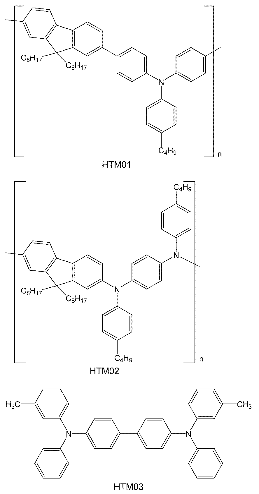
発光材料は、発光層において、正孔および電子を利用して行う発光に直接または間接に寄与する機能を有する。なお、本明細書において、「発光」には、蛍光による発光および燐光による発光を含むものとする。
ホスト材料は、通常、発光層に注入された正孔および電子を輸送する機能を有する。
ドーパント材料は、輸送された正孔および電子を再結合することにより得られるエネルギーを利用して発光する機能を有する。
レベリング剤は、有機発光素子用インク組成物を用いて形成される塗膜表面に配向し、塗膜の乾燥の際に第1の溶媒の優先的な蒸発を抑制または防止する機能を有する。
シロキサンモノマーは、シロキサン基、重合性官能基、および第1の連結基を含む。この際、前記第1の連結基は、前記シロキサン基と前記重合性官能基とを連結させるものである。なお、本明細書において、「シロキサン」とは、「-Si-O-Si-」の構造(シロキサン構造)を意味する。


芳香族含有モノマーは、芳香族溶媒との親和性を向上させる機能を有する。これにより、レベリング剤が好適に溶解しうる。その結果、有機発光素子用インク組成物が塗布しやすくなるとともに、得られる塗膜が平坦性を有しうる。
疎水性モノマーは、レベリング剤の性能を調整する機能を有する。
重合開始剤は、通常、重合体を形成する際に適用される重合反応の開始剤の機能を有する。この際、重合開始剤は、シロキサンモノマーの重合性官能基、芳香族含有モノマーの重合性官能基、疎水性モノマーの重合性官能基等と反応して重合を開始させることができる。この場合には、得られる重合体には、重合開始剤に起因する成分が含まることがある。
本形態に係るレベリング剤は、少なくともシロキサンモノマーを単量体単位として含む重合体である。当該重合体は、単独重合体であっても、共重合体であってもよい。この際、前記共重合体は、ランダム共重合体であっても、交互重合体であっても、グラフト共重合体であっても、ブロック共重合体であってもよい。これらのうち、レベリング剤は、共重合体であることが好ましく、ランダム重合体、ブロック共重合体であることがより好ましく、ブロック共重合体であることがさらに好ましい。レベリング剤がブロック共重合体であると、レベリング剤の機能、具体的には第1の溶媒の優先的な蒸発の抑制または防止効果および/または層のうねりの発生の抑制または防止効果を好適に実現することができる。より詳細には、レベリング剤がブロック共重合体であることにより、ランダム共重合体を使用した場合と比較して、シロキサン構造が部分的に偏在することから、レベリング剤の機能が好適に発揮される。また、レベリング剤を構成するシロキサン構造と、芳香族含有モノマー由来構造および/または疎水性モノマー由来構造とが偏在すると、シロキサン構造については塗膜表面に配向し、芳香族含有モノマー由来構造および/または疎水性モノマー由来構造については塗膜内部に配向する傾向が高まるため、レベリング剤の機能がより好適に発揮されうる。
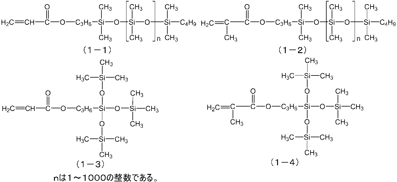

レベリング剤は、特に制限されず、公知の方法により製造される。
第1の溶媒は、有機発光素子用インク組成物の表面張力を低下させる機能を有する。
芳香族溶媒は、有機発光素子用インク組成物に含有される第1の有機発光素子材料を溶媒させる機能を有する。
一実施形態において、有機発光素子用インク組成物のぬれ性を確保する観点から、第1の溶媒および芳香族溶媒の種類、混合比を調整することが好ましい。


本発明の一実施形態において、有機発光素子用インク組成物の製造方法は、特に制限されないが、(1)レベリング剤および溶媒(第1の溶媒および芳香族溶媒)を含む溶液または分散液を調製し、次いで、当該溶液または分散液に第1の有機発光素子材料を添加する方法、(2)第1の有機発光素子材料および溶媒(第1の溶媒および芳香族溶媒)を含む溶液または分散液を調製し、次いで、当該溶液または分散液にレベリング剤を添加する方法、(3)レベリング剤および溶媒(第1の溶媒および/または芳香族溶媒)を含む溶液または分散液と、第1の有機発光素子材料および溶媒(芳香族溶媒および/または第1の溶媒)を含む溶液または分散液と、をそれぞれ調製し、これらの溶液または分散液を混合する方法等が挙げられる。
本発明の一実施形態によれば、有機半導体素子が提供される。この際、前記有機半導体素子は、第2の有機半導体素子材料を含む第2の層と、第1の有機半導体素子材料およびレベリング剤を含み、前記第2の層の直上に配置される第1の層と、を有する。この際、第2の層の表面エネルギーが28mN/m以下である。また、前記レベリング剤が、少なくともシロキサンモノマーを単量体単位として含む重合体である。
第2の層の表面エネルギーは28mN/m以下であり、好ましくは18~25mN/mであり、より好ましくは18~23mN/mである。
第2の層形成用インク組成物は、通常、第2の有機発光素子材料、レベリング剤(以下、「第2の層形成用レベリング剤」とも称することがある)、および第2の溶媒を含む。
第2の層は、その直上に湿式成膜法により第1の層が形成されうることから、通常、正孔注入層、正孔輸送層、発光層、電子輸送層、電子注入層であり、好ましくは正孔注入層、正孔輸送層である。したがって、第2の有機発光素子材料は、好ましくは、正孔注入層に使用される正孔注入料、正孔輸送層に使用される正孔輸送材料である。
正孔注入材料は、正孔注入層において、陽極から正孔を取り入れる機能を有する。この際、正孔注入材料が取り入れた正孔は、正孔輸送層または発光層に輸送される。
正孔輸送材料としては、上述したものが用いられうることからここでは説明を省略する。
第2の層は、レベリング剤を含んでいてもよい。
第2の溶媒は、特に制限されず、形成する層に応じて適宜公知のものが使用されうる。具体的には、芳香族系溶媒、アルカン系溶媒、エーテル系溶媒、アルコール系溶媒、エステル系溶媒、アミド系溶媒、他の溶媒等が挙げられる。
第2の層の形成方法は、特に制限されないが、上述の第2の層形成用インク組成物を塗布、乾燥する方法が挙げられる。この際、塗布、乾燥条件等は特に制限されず、公知の技術が適宜採用されうる。
第2の層は、第2の有機発光素子材料を含む。
第1の層は、第2の層の直上に配置される。
陽極としては、特に制限されないが、金(Au)等の金属、ヨウ化銅(CuI)、インジウムスズ酸化物(ITO)、酸化スズ(SnO2)、酸化亜鉛(ZnO)等が用いられうる。これらの材料は、単独で用いても、2種以上を組み合わせて用いてもよい。
正孔注入層は、有機発光素子において任意の構成要素であり、陽極から正孔を取り入れる機能を有する。通常、陽極から取り入れた正孔は、正孔輸送層または発光層に輸送される。
正孔輸送層は、有機発光素子において任意の構成要素であり、正孔を効率的に輸送する機能を有する。また、正孔輸送層は、正孔の輸送を防止する機能を有しうる。正孔輸送層は、通常、陽極または正孔注入層から正孔を取り入れ、発光層に正孔を輸送する。
発光層は、発光層に注入された正孔および電子の再結合により生じるエネルギーを利用して発光を生じさせる機能を有する。
電子輸送層は、有機発光素子において任意の構成要素であり、電子を効率的に輸送する機能を有する。また、電子輸送層は、電子の輸送を防止する機能を有しうる。電子輸送層は、通常、陰極または電子注入層から電子を取り入れ、発光層に電子を輸送する。
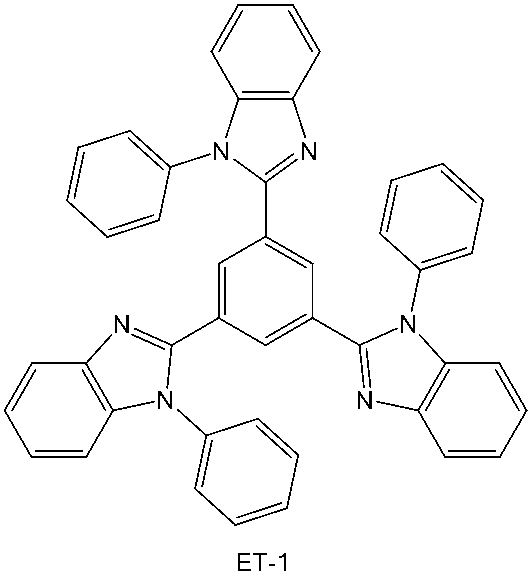
電子注入層は、有機発光素子において任意の構成要素であり、陰極から電子を取り入れる機能を有する。通常、陰極から取り入れた電子は、電子輸送層または発光層に輸送される。
陰極としては、特に制限されないが、リチウム、ナトリウム、マグネシウム、アルミニウム、ナトリウム-カリウム合金、マグネシウム/アルミニウム混合物、マグネシウム/インジウム混合物、アルミニウム/酸化アルミニウム(Al2O3)混合物、希土類金属等が挙げられる。これらの材料は、単独で用いても、2種以上を組み合わせて用いてもよい。
下記式で表されるレべリング剤MCS-01(ポリエーテル変性シリコーンオイル、ランダム重合体)0.005部と、第1の溶媒であるトリフルオロメトキシベンゼン(TFMB、表面張力:22mN/M)50部と、芳香族溶媒であるテトラリン(表面張力:35mN/M)50部と、を混合して、混合液を調製した。なお、MCS-01は白金触媒存在下、メチルハイドロジェンシリコーンオイルとアルケニル化合物を反応させることで合成した。


第1の溶媒を、それぞれオクタン(表面張力:21mN/M)、ノナン(表面張力:22mN/M)、デカン(表面張力:23mN/M)、ウンデカン(表面張力:24mN/M)、ドデカン(表面張力:25mN/M)、メチルエチルケトン(MEK、表面張力:24.6mN/M)、メチルイソブチルケトン(MIBK、表面張力:23.6mN/M)、ジイソブチルケトン(DIBK、表面張力:23.9mN/M)、およびジブチルエーテル(表面張力:22.4mN/M)に変更したことを除いては、実施例1と同様の方法で有機発光素子用インク組成物を製造した。
レベリング剤を、下記式で表されるレべリング剤MCS-02(アラルキル変性シリコーンオイル、ランダム重合体、芳香族含有モノマーを含むに変更したことを除いては、実施例1と同様の方法で有機発光素子用インク組成物を製造した。なお、MCS-02は使用するモノマーを変更したことを除いては、実施例1と同様の方法で合成した。

溶媒を、それぞれデカン(表面張力:23mN/M)およびメチルイソブチルケトン(MIBK、表面張力:23.6mN/M)に変更したことを除いては、実施例11と同様の方法で有機発光素子用インク組成物を製造した。
レベリング剤を、MCS-01と同様に合成した下記式で表されるレべリング剤MCS-03(アラルキル変性シリコーンオイル、ランダム重合体、芳香族含有モノマーを含む)に変更したことを除いては、実施例1と同様の方法で有機発光素子用インク組成物を製造した。

溶媒を、それぞれデカン(表面張力:23mN/M)およびメチルイソブチルケトン(MIBK、表面張力:23.6mN/M)に変更したことを除いては、実施例14と同様の方法で有機発光素子用インク組成物を製造した。
レベリング剤を、下記式で表されるSP01(ブロック重合体、芳香族含有モノマーを含む)に変更したことを除いては、実施例1と同様の方法で有機発光素子用インク組成物を製造した。SP01はシリコーンマクロマーFM0711(JNC株式会社)とスチレンを用い、n-ブチルリチウムによるリビングアニオン重合により合成した。

第1の溶媒を、それぞれデカン(表面張力:23mN/M)、メチルイソブチルケトン(MIBK、表面張力:23.6mN/M)、およびジブチルエーテル(表面張力:22.4mN/M)に変更したことを除いては、実施例17と同様の方法で有機発光素子用インク組成物を製造した。
レベリング剤を、SP01と同様に合成した下記式で表されるSP02(ブロック重合体、芳香族含有モノマーを含む、)に変更したことを除いては、実施例1と同様の方法で有機発光素子用インク組成物を製造した。

第1の溶媒を、それぞれデカン(表面張力:23mN/M)、メチルイソブチルケトン(MIBK、表面張力:23.6mN/M)、およびジブチルエーテル(表面張力:22.4mN/M)に変更したことを除いては、実施例21と同様の方法で有機発光素子用インク組成物を製造した。
レベリング剤を、下記式で表されるSP03(ランダム重合体、芳香族含有モノマーを含む、)に変更したことを除いては、実施例1と同様の方法で有機発光素子用インク組成物を製造した。なお、SP03はシリコーンマクロマーFM0711(JNC株式会社)とスチレンを用い、t-ブチルペルオキシベンゾエートにより重合、合成した。

レベリング剤を、下記式で表されるSP04(ブロック重合体、芳香族含有モノマーを含む、)に変更したことを除いては、実施例1と同様の方法で有機発光素子用インク組成物を製造した。なお、SP04は、使用するモノマーを変更したことを除いては、実施例25のSP03と同様の方法で合成した。
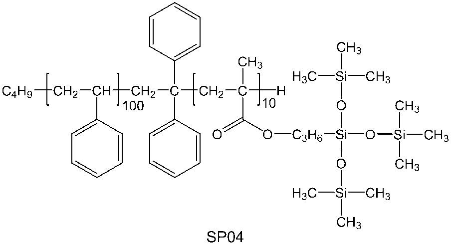
芳香族溶媒を、アミルベンゼン(表面張力:29mN/M)に変更したことを除いては、実施例1と同様の方法で有機発光素子用インク組成物を製造した。
第1の溶媒を、それぞれウンデカン(表面張力:24mN/M)およびジイソブチルケトン(DIBK、表面張力:23.9mN/M)に変更したことを除いては、実施例27と同様の方法で有機発光素子用インク組成物を製造した。
芳香族溶媒を、キシレン(表面張力:29mN/M)、メシチレン(表面張力:28mN/M)、シクロヘキシルベンゼン(表面張力:34mN/M)、1-メチルナフタレン(表面張力:39mN/M)、ブチルフェニルエーテル(表面張力:31mN/M)、および安息香酸エチル(表面張力:35mN/M)に変更したことを除いては、実施例8と同様の方法で有機発光素子用インク組成物を製造した。
芳香族溶媒を、アミルベンゼン(表面張力:29mN/M)、キシレン(表面張力:29mN/M)、メシチレン(表面張力:28mN/M)、シクロヘキシルベンゼン(表面張力:34mN/M)、1-メチルナフタレン(表面張力:39mN/M)、ブチルフェニルエーテル(表面張力:31mN/M)、および安息香酸エチル(表面張力:35mN/M)に変更したことを除いては、実施例19と同様の方法で有機発光素子用インク組成物を製造した。
正孔輸送材料を、下記式で表されるHTM02(ADS社製)に変更したことを除いては、実施例17と同様の方法で有機発光素子用インク組成物を製造した。
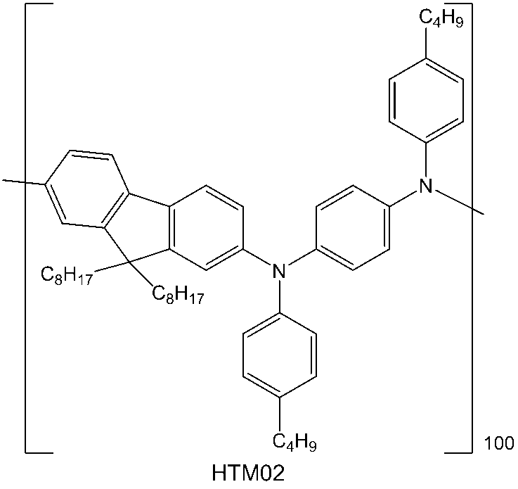
第1の溶媒を、それぞれデカン(表面張力:23mN/M)、メチルイソブチルケトン(MIBK、表面張力:23.6mN/M)、およびジイソブチルケトン(DIBK、表面張力:23.9mN/M)に変更したことを除いては、実施例43と同様の方法で有機発光素子用インク組成物を製造した。
正孔輸送材料を、下記式で表されるHTM03(東京化成工業社製)に変更したことを除いては、実施例17と同様の方法で有機発光素子用インク組成物を製造した。
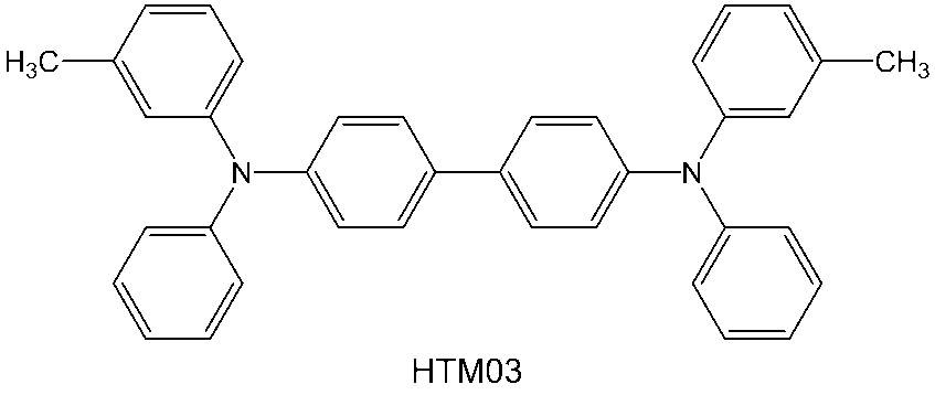
第1の溶媒を、それぞれデカン(表面張力:23mN/M)、メチルイソブチルケトン(MIBK、表面張力:23.6mN/M)、およびジイソブチルケトン(DIBK、表面張力:23.9mN/M)に変更したことを除いては、実施例47と同様の方法で有機発光素子用インク組成物を製造した。
レべリング剤であるMCS-01(ポリエーテル変性シリコーンオイル、ランダム重合体)0.005部と、芳香族溶媒であるテトラリン(表面張力:35mN/M)100部と、を混合して、混合液を調製した。
レべリング剤であるSP01(ブロック重合体、芳香族含有モノマーを含む、)0.005部と、芳香族溶媒であるテトラリン(表面張力:35mN/M)100部と、を混合して、混合液を調製した。
実施例1~50および比較例1~3で製造した有機発光素子用インク組成物を用いた性能評価を行った。
低表面エネルギー膜を作製し、当該低表面エネルギー膜上における有機発光素子用インク組成物の接触角を評価した。
△:28度超30度以下
○:26度超28度以下
◎:26度以下
有機発光素子を作製し、得られた有機発光素子についての輝度ムラを測定した。

△:輝度のバラツキ率が50%超70%以下である
○:輝度のバラツキ率が30%超50%以下である
◎:輝度のバラツキ率が20%超30%以下である
◎◎:輝度のバラツキ率が20%以下である


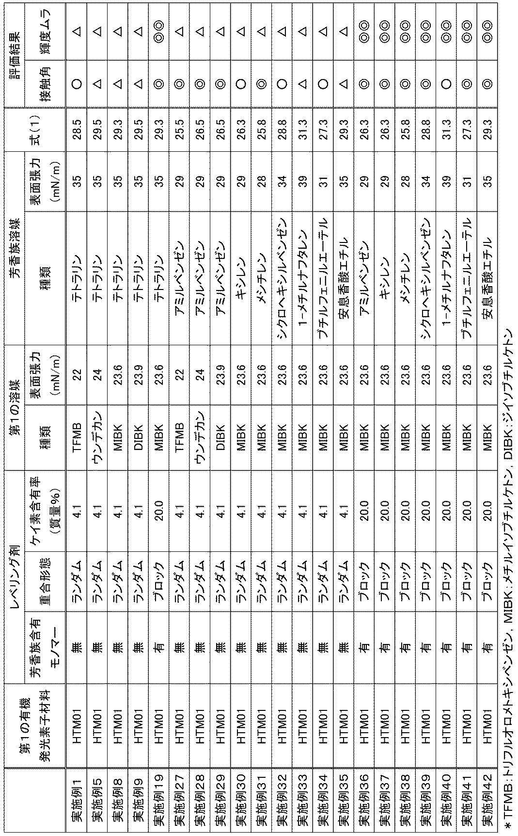
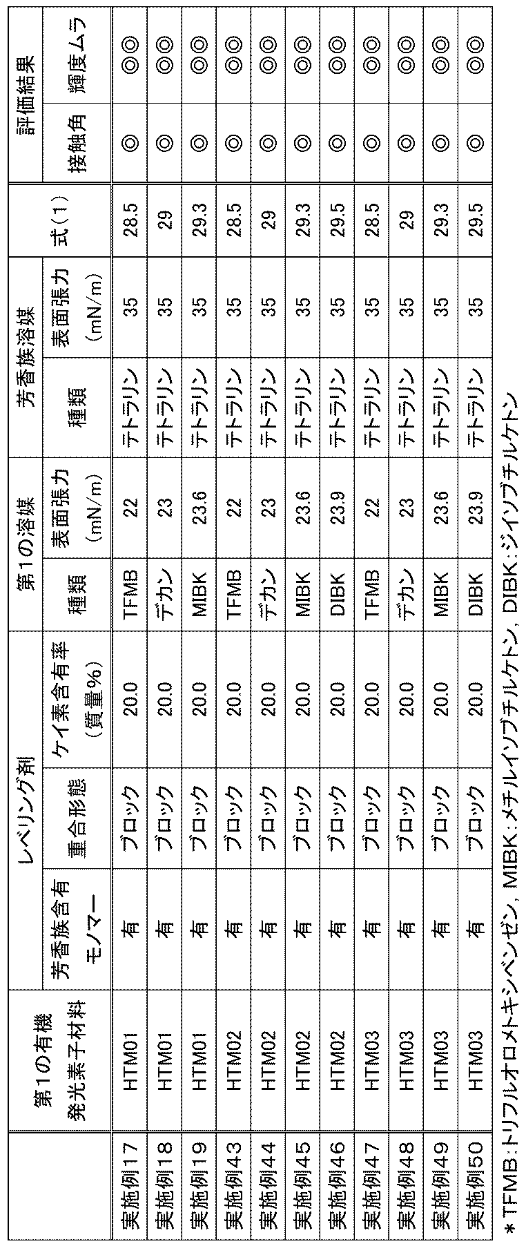
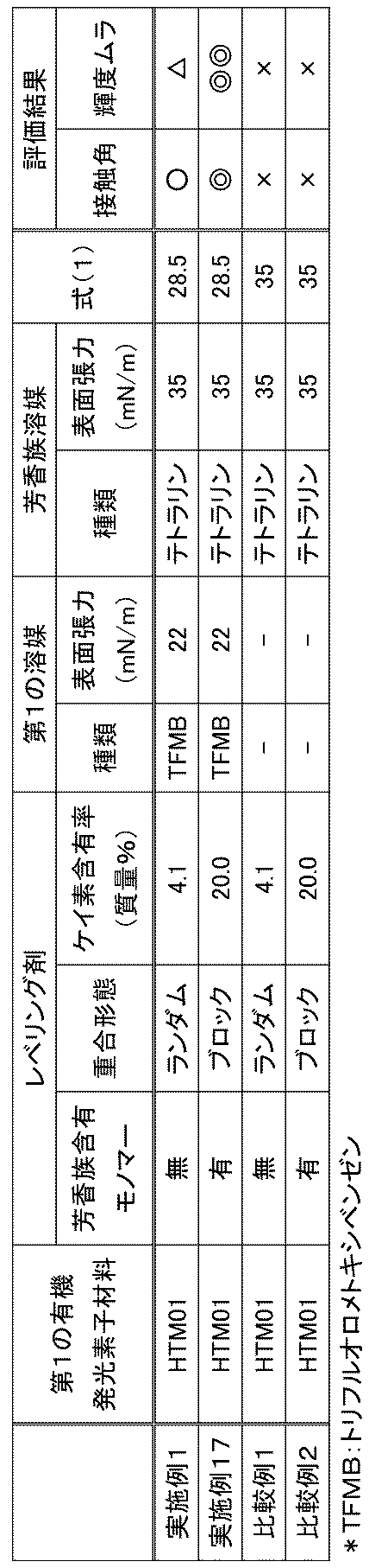
Claims (12)
- 第1の有機半導体素子材料、レベリング剤、第1の溶媒、および芳香族溶媒を含み、
前記レベリング剤が、少なくともシロキサンモノマーを単量体単位として含む重合体であり、
前記第1の溶媒の表面張力が25mN/m以下である、有機半導体素子用インク組成物。 - 前記レベリン-グ剤が、芳香族含有モノマーを単量体単位としてさらに含む、請求項1に記載の有機半導体素子用インク組成物。
- 前記レベリング剤が、ブロック共重合体を含む、請求項1または2に記載の有機半導体素子用インク組成物。
- 前記レベリング剤のケイ素含有率が、10質量%以上である、請求項1~3のいずれか1項に記載の有機半導体素子用インク組成物。
- 前記第1の溶媒の表面張力が、23mN/m未満である、請求項1~4のいずれか1項に記載の有機半導体素子用インク組成物。
- 前記芳香族溶媒の表面張力が、36mN/m未満である、請求項1~5のいずれか1項に記載の有機半導体素子用インク組成物。
- 下記式(1):

で表される溶媒表面エネルギーAが、30未満である、請求項1~6のいずれか1項に記載の有機半導体素子用インク組成物。 - 前記第1の有機半導体素子材料が、正孔輸送材料である、請求項1~7に記載の有機半導体素子用インク組成物。
- 前記有機半導体が、有機発光素子である、請求項1~8のいずれか1項に記載の有機半導体素子用インク組成物。
- 第2の有機半導体素子材料を含む第2の層と、
第1の有機半導体素子材料およびレベリング剤を含み、前記第2の層の直上に配置される第1の層と、を有し、
前記第2の層の表面エネルギーが28mN/m以下であり、
前記レベリング剤が、少なくともシロキサンモノマーを単量体単位として含む重合体である、有機半導体素子。 - 前記第1の有機半導体素子材料が、正孔輸送材料である、請求項10または11に記載の有機半導体素子。
- 有機発光素子である、請求項12に記載の有機半導体素子。
Priority Applications (4)
| Application Number | Priority Date | Filing Date | Title |
|---|---|---|---|
| US15/754,149 US20180248122A1 (en) | 2015-08-24 | 2016-08-18 | Ink composition for organic semiconductor device and organic semiconductor device including the same |
| JP2017536384A JP6439877B2 (ja) | 2015-08-24 | 2016-08-18 | 有機半導体素子用インク組成物およびこれを用いた有機半導体素子 |
| KR1020187005244A KR20180044286A (ko) | 2015-08-24 | 2016-08-18 | 유기 반도체 소자용 잉크 조성물 및 이것을 사용한 유기 반도체 소자 |
| CN201680048909.1A CN107926094A (zh) | 2015-08-24 | 2016-08-18 | 有机半导体元件用油墨组合物和使用其的有机半导体元件 |
Applications Claiming Priority (2)
| Application Number | Priority Date | Filing Date | Title |
|---|---|---|---|
| JP2015164779 | 2015-08-24 | ||
| JP2015-164779 | 2015-08-24 |
Publications (1)
| Publication Number | Publication Date |
|---|---|
| WO2017033828A1 true WO2017033828A1 (ja) | 2017-03-02 |
Family
ID=58100112
Family Applications (1)
| Application Number | Title | Priority Date | Filing Date |
|---|---|---|---|
| PCT/JP2016/074095 Ceased WO2017033828A1 (ja) | 2015-08-24 | 2016-08-18 | 有機半導体素子用インク組成物およびこれを用いた有機半導体素子 |
Country Status (6)
| Country | Link |
|---|---|
| US (1) | US20180248122A1 (ja) |
| JP (1) | JP6439877B2 (ja) |
| KR (1) | KR20180044286A (ja) |
| CN (1) | CN107926094A (ja) |
| TW (1) | TW201714986A (ja) |
| WO (1) | WO2017033828A1 (ja) |
Cited By (2)
| Publication number | Priority date | Publication date | Assignee | Title |
|---|---|---|---|---|
| WO2019078080A1 (ja) * | 2017-10-20 | 2019-04-25 | Dic株式会社 | レベリング剤、機能層形成用インク組成物及び積層電子部品 |
| JPWO2022064584A1 (ja) * | 2020-09-24 | 2022-03-31 |
Families Citing this family (4)
| Publication number | Priority date | Publication date | Assignee | Title |
|---|---|---|---|---|
| CN118496480A (zh) * | 2018-11-05 | 2024-08-16 | 康宁股份有限公司 | 用于有机薄膜晶体管的可uv图案化的聚合物掺混物 |
| CN115246922B (zh) * | 2021-04-28 | 2024-06-04 | 财团法人工业技术研究院 | 聚合物及包含其的发光装置 |
| US11912816B2 (en) | 2021-04-28 | 2024-02-27 | Industrial Technology Research Institute | Polymer and light-emitting device |
| CN115440409B (zh) * | 2022-09-05 | 2025-09-05 | 宁夏大学 | 一种N-TOPCon太阳电池用银铝浆及其制备方法和应用 |
Citations (4)
| Publication number | Priority date | Publication date | Assignee | Title |
|---|---|---|---|---|
| JPH08504674A (ja) * | 1993-04-28 | 1996-05-21 | ユニヴァーシティ オブ ニュー メキシコ | 化学表面改質による高気孔質キセロゲルの製造 |
| JP2010070511A (ja) * | 2008-09-19 | 2010-04-02 | Mitsubishi Chemicals Corp | エナミン系化合物、該化合物を用いた電子写真感光体および画像形成装置 |
| JP2013126364A (ja) * | 2011-12-16 | 2013-06-24 | Toyota Industries Corp | 振動アクチュエータ |
| JP2014205830A (ja) * | 2013-03-21 | 2014-10-30 | 国立大学法人九州大学 | 有機半導体含有層形成用レベリング剤、有機半導体含有層形成用組成物、並びに、有機デバイス及びその製造方法 |
Family Cites Families (9)
| Publication number | Priority date | Publication date | Assignee | Title |
|---|---|---|---|---|
| CN101020796A (zh) * | 2007-03-23 | 2007-08-22 | 友达光电股份有限公司 | 一种油墨组成物 |
| JP4475305B2 (ja) * | 2007-09-06 | 2010-06-09 | セイコーエプソン株式会社 | 配向膜形成用組成物、液晶装置の製造方法 |
| JP2009080454A (ja) * | 2007-09-06 | 2009-04-16 | Seiko Epson Corp | 配向膜形成用組成物、液晶装置の製造方法 |
| KR20100004258A (ko) * | 2008-07-03 | 2010-01-13 | 포항공과대학교 산학협력단 | 잉크젯 프린트 잉크 및 이를 이용한 유기박막 트랜지스터 |
| JP2010067543A (ja) * | 2008-09-12 | 2010-03-25 | Sumitomo Chemical Co Ltd | 印刷用のインキ |
| JP2012054209A (ja) * | 2010-09-03 | 2012-03-15 | Sumitomo Metal Mining Co Ltd | 導電性酸化物微粒子分散液と透明導電膜形成用塗布液、及び透明導電膜 |
| JP6225413B2 (ja) * | 2012-11-16 | 2017-11-08 | セイコーエプソン株式会社 | 機能層形成用インク、インク容器、吐出装置、機能層の形成方法、有機el素子の製造方法 |
| KR20180108917A (ko) * | 2013-10-31 | 2018-10-04 | 카티바, 인크. | 잉크젯 인쇄를 위한 폴리티오펜-포함 잉크 조성물 |
| CN105315757B (zh) * | 2015-12-06 | 2017-02-01 | 广州市斯洛柯高分子聚合物有限公司 | 一种有机硅流平剂及其制备方法 |
-
2016
- 2016-08-18 WO PCT/JP2016/074095 patent/WO2017033828A1/ja not_active Ceased
- 2016-08-18 JP JP2017536384A patent/JP6439877B2/ja not_active Expired - Fee Related
- 2016-08-18 US US15/754,149 patent/US20180248122A1/en not_active Abandoned
- 2016-08-18 CN CN201680048909.1A patent/CN107926094A/zh active Pending
- 2016-08-18 KR KR1020187005244A patent/KR20180044286A/ko not_active Withdrawn
- 2016-08-22 TW TW105126756A patent/TW201714986A/zh unknown
Patent Citations (4)
| Publication number | Priority date | Publication date | Assignee | Title |
|---|---|---|---|---|
| JPH08504674A (ja) * | 1993-04-28 | 1996-05-21 | ユニヴァーシティ オブ ニュー メキシコ | 化学表面改質による高気孔質キセロゲルの製造 |
| JP2010070511A (ja) * | 2008-09-19 | 2010-04-02 | Mitsubishi Chemicals Corp | エナミン系化合物、該化合物を用いた電子写真感光体および画像形成装置 |
| JP2013126364A (ja) * | 2011-12-16 | 2013-06-24 | Toyota Industries Corp | 振動アクチュエータ |
| JP2014205830A (ja) * | 2013-03-21 | 2014-10-30 | 国立大学法人九州大学 | 有機半導体含有層形成用レベリング剤、有機半導体含有層形成用組成物、並びに、有機デバイス及びその製造方法 |
Cited By (4)
| Publication number | Priority date | Publication date | Assignee | Title |
|---|---|---|---|---|
| WO2019078080A1 (ja) * | 2017-10-20 | 2019-04-25 | Dic株式会社 | レベリング剤、機能層形成用インク組成物及び積層電子部品 |
| JPWO2022064584A1 (ja) * | 2020-09-24 | 2022-03-31 | ||
| WO2022064584A1 (ja) * | 2020-09-24 | 2022-03-31 | シャープ株式会社 | 表示素子 |
| JP7352749B2 (ja) | 2020-09-24 | 2023-09-28 | シャープ株式会社 | 表示素子 |
Also Published As
| Publication number | Publication date |
|---|---|
| US20180248122A1 (en) | 2018-08-30 |
| JPWO2017033828A1 (ja) | 2018-07-26 |
| KR20180044286A (ko) | 2018-05-02 |
| CN107926094A (zh) | 2018-04-17 |
| TW201714986A (zh) | 2017-05-01 |
| JP6439877B2 (ja) | 2018-12-19 |
Similar Documents
| Publication | Publication Date | Title |
|---|---|---|
| JP6439877B2 (ja) | 有機半導体素子用インク組成物およびこれを用いた有機半導体素子 | |
| TWI618689B (zh) | Organic electronic materials, ink compositions, and organic electronic components | |
| JP6341436B2 (ja) | 有機発光素子用インク組成物およびこれを用いた有機発光素子 | |
| JP7415917B2 (ja) | 組成物、および有機電界発光素子の製造方法 | |
| TWI710609B (zh) | 印墨組成物及製造有機發光裝置的方法 | |
| CN103459375A (zh) | 有机化合物、电荷传输材料、含有该化合物的组合物、有机场致发光元件、显示装置及照明装置 | |
| JP2012109286A (ja) | 有機電界発光素子用組成物、有機電界発光素子、有機elディスプレイ及び有機el照明 | |
| JPWO2019177175A1 (ja) | 重合体、有機電界発光素子用組成物、有機電界発光素子、有機el表示装置、有機el照明及び有機電界発光素子の製造方法 | |
| JP2019057484A (ja) | 有機電界発光素子、有機電界発光素子の製造方法 | |
| CN101641422B (zh) | 具有硅和/或锡的乙烯基类聚合物及使用该聚合物的有机发光二极管 | |
| WO2019078080A1 (ja) | レベリング剤、機能層形成用インク組成物及び積層電子部品 | |
| WO2022163199A1 (ja) | 有機エレクトロルミネッセンス素子、その製造方法、並びにそれを具備した照明装置、表示装置及び印刷造形物 | |
| WO2017104173A1 (ja) | 複素環含有シロキサン重合体、該重合体を含有する組成物、電子素子 | |
| JPWO2023085170A5 (ja) | ||
| WO2023085170A1 (ja) | 組成物、および有機電界発光素子の製造方法 | |
| JP2023130237A (ja) | 有機電界発光素子の製造方法、及び有機電界発光素子 | |
| JP6245411B2 (ja) | シロキサンモノマーおよびその重合体、該重合体を含有する組成物、電子素子 | |
| JP2016058576A (ja) | 有機発光素子用インク組成物およびこれを用いた有機発光素子 | |
| US20220285623A1 (en) | Inkjet recording medium for organic semiconductor device, member for organic semiconductor device, and manufacturing method for organic semiconductor device | |
| JP2023130238A (ja) | 有機電界発光素子の製造方法及び有機電界発光素子 | |
| WO2024096035A1 (ja) | 有機電界発光素子、有機電界発光素子を製造する方法、有機elディスプレイパネル、有機elディスプレイパネルを製造する方法、有機電界発光素子の膜厚構成の設計方法及び有機elディスプレイパネルの膜厚構成の設計方法 | |
| JP5141229B2 (ja) | 外縁規定膜形成用組成物、機能膜の製造方法、有機電界発光素子及びその製造方法、並びに画像表示デバイス |
Legal Events
| Date | Code | Title | Description |
|---|---|---|---|
| 121 | Ep: the epo has been informed by wipo that ep was designated in this application |
Ref document number: 16839175 Country of ref document: EP Kind code of ref document: A1 |
|
| ENP | Entry into the national phase |
Ref document number: 2017536384 Country of ref document: JP Kind code of ref document: A |
|
| WWE | Wipo information: entry into national phase |
Ref document number: 15754149 Country of ref document: US |
|
| ENP | Entry into the national phase |
Ref document number: 20187005244 Country of ref document: KR Kind code of ref document: A |
|
| NENP | Non-entry into the national phase |
Ref country code: DE |
|
| 122 | Ep: pct application non-entry in european phase |
Ref document number: 16839175 Country of ref document: EP Kind code of ref document: A1 |