WO2017033244A1 - 電子装置 - Google Patents
電子装置 Download PDFInfo
- Publication number
- WO2017033244A1 WO2017033244A1 PCT/JP2015/073628 JP2015073628W WO2017033244A1 WO 2017033244 A1 WO2017033244 A1 WO 2017033244A1 JP 2015073628 W JP2015073628 W JP 2015073628W WO 2017033244 A1 WO2017033244 A1 WO 2017033244A1
- Authority
- WO
- WIPO (PCT)
- Prior art keywords
- wiring
- wiring board
- power
- width
- electrically connected
- Prior art date
- Legal status (The legal status is an assumption and is not a legal conclusion. Google has not performed a legal analysis and makes no representation as to the accuracy of the status listed.)
- Ceased
Links
Images









Classifications
-
- H—ELECTRICITY
- H02—GENERATION; CONVERSION OR DISTRIBUTION OF ELECTRIC POWER
- H02K—DYNAMO-ELECTRIC MACHINES
- H02K11/00—Structural association of dynamo-electric machines with electric components or with devices for shielding, monitoring or protection
- H02K11/30—Structural association with control circuits or drive circuits
- H02K11/33—Drive circuits, e.g. power electronics
-
- H—ELECTRICITY
- H05—ELECTRIC TECHNIQUES NOT OTHERWISE PROVIDED FOR
- H05K—PRINTED CIRCUITS; CASINGS OR CONSTRUCTIONAL DETAILS OF ELECTRIC APPARATUS; MANUFACTURE OF ASSEMBLAGES OF ELECTRICAL COMPONENTS
- H05K1/00—Printed circuits
- H05K1/18—Printed circuits structurally associated with non-printed electric components
- H05K1/181—Printed circuits structurally associated with non-printed electric components associated with surface mounted components
-
- F—MECHANICAL ENGINEERING; LIGHTING; HEATING; WEAPONS; BLASTING
- F02—COMBUSTION ENGINES; HOT-GAS OR COMBUSTION-PRODUCT ENGINE PLANTS
- F02M—SUPPLYING COMBUSTION ENGINES IN GENERAL WITH COMBUSTIBLE MIXTURES OR CONSTITUENTS THEREOF
- F02M37/00—Apparatus or systems for feeding liquid fuel from storage containers to carburettors or fuel-injection apparatus; Arrangements for purifying liquid fuel specially adapted for, or arranged on, internal-combustion engines
- F02M37/04—Feeding by means of driven pumps
- F02M37/08—Feeding by means of driven pumps electrically driven
-
- H—ELECTRICITY
- H02—GENERATION; CONVERSION OR DISTRIBUTION OF ELECTRIC POWER
- H02M—APPARATUS FOR CONVERSION BETWEEN AC AND AC, BETWEEN AC AND DC, OR BETWEEN DC AND DC, AND FOR USE WITH MAINS OR SIMILAR POWER SUPPLY SYSTEMS; CONVERSION OF DC OR AC INPUT POWER INTO SURGE OUTPUT POWER; CONTROL OR REGULATION THEREOF
- H02M7/00—Conversion of AC power input into DC power output; Conversion of DC power input into AC power output
- H02M7/003—Constructional details, e.g. physical layout, assembly, wiring or busbar connections
-
- H—ELECTRICITY
- H02—GENERATION; CONVERSION OR DISTRIBUTION OF ELECTRIC POWER
- H02M—APPARATUS FOR CONVERSION BETWEEN AC AND AC, BETWEEN AC AND DC, OR BETWEEN DC AND DC, AND FOR USE WITH MAINS OR SIMILAR POWER SUPPLY SYSTEMS; CONVERSION OF DC OR AC INPUT POWER INTO SURGE OUTPUT POWER; CONTROL OR REGULATION THEREOF
- H02M7/00—Conversion of AC power input into DC power output; Conversion of DC power input into AC power output
- H02M7/42—Conversion of DC power input into AC power output without possibility of reversal
- H02M7/44—Conversion of DC power input into AC power output without possibility of reversal by static converters
- H02M7/48—Conversion of DC power input into AC power output without possibility of reversal by static converters using discharge tubes with control electrode or semiconductor devices with control electrode
-
- H—ELECTRICITY
- H02—GENERATION; CONVERSION OR DISTRIBUTION OF ELECTRIC POWER
- H02M—APPARATUS FOR CONVERSION BETWEEN AC AND AC, BETWEEN AC AND DC, OR BETWEEN DC AND DC, AND FOR USE WITH MAINS OR SIMILAR POWER SUPPLY SYSTEMS; CONVERSION OF DC OR AC INPUT POWER INTO SURGE OUTPUT POWER; CONTROL OR REGULATION THEREOF
- H02M7/00—Conversion of AC power input into DC power output; Conversion of DC power input into AC power output
- H02M7/42—Conversion of DC power input into AC power output without possibility of reversal
- H02M7/44—Conversion of DC power input into AC power output without possibility of reversal by static converters
- H02M7/48—Conversion of DC power input into AC power output without possibility of reversal by static converters using discharge tubes with control electrode or semiconductor devices with control electrode
- H02M7/53—Conversion of DC power input into AC power output without possibility of reversal by static converters using discharge tubes with control electrode or semiconductor devices with control electrode using devices of a triode or transistor type requiring continuous application of a control signal
- H02M7/537—Conversion of DC power input into AC power output without possibility of reversal by static converters using discharge tubes with control electrode or semiconductor devices with control electrode using devices of a triode or transistor type requiring continuous application of a control signal using semiconductor devices only, e.g. single switched pulse inverters
- H02M7/5387—Conversion of DC power input into AC power output without possibility of reversal by static converters using discharge tubes with control electrode or semiconductor devices with control electrode using devices of a triode or transistor type requiring continuous application of a control signal using semiconductor devices only, e.g. single switched pulse inverters in a bridge configuration
- H02M7/53871—Conversion of DC power input into AC power output without possibility of reversal by static converters using discharge tubes with control electrode or semiconductor devices with control electrode using devices of a triode or transistor type requiring continuous application of a control signal using semiconductor devices only, e.g. single switched pulse inverters in a bridge configuration with automatic control of output voltage or current
- H02M7/53875—Conversion of DC power input into AC power output without possibility of reversal by static converters using discharge tubes with control electrode or semiconductor devices with control electrode using devices of a triode or transistor type requiring continuous application of a control signal using semiconductor devices only, e.g. single switched pulse inverters in a bridge configuration with automatic control of output voltage or current with analogue control of three-phase output
-
- H—ELECTRICITY
- H02—GENERATION; CONVERSION OR DISTRIBUTION OF ELECTRIC POWER
- H02P—CONTROL OR REGULATION OF ELECTRIC MOTORS, ELECTRIC GENERATORS OR DYNAMO-ELECTRIC CONVERTERS; CONTROLLING TRANSFORMERS, REACTORS OR CHOKE COILS
- H02P27/00—Arrangements or methods for the control of AC motors characterised by the kind of supply voltage
- H02P27/04—Arrangements or methods for the control of AC motors characterised by the kind of supply voltage using variable-frequency supply voltage, e.g. inverter or converter supply voltage
- H02P27/06—Arrangements or methods for the control of AC motors characterised by the kind of supply voltage using variable-frequency supply voltage, e.g. inverter or converter supply voltage using DC to AC converters or inverters
-
- H—ELECTRICITY
- H02—GENERATION; CONVERSION OR DISTRIBUTION OF ELECTRIC POWER
- H02P—CONTROL OR REGULATION OF ELECTRIC MOTORS, ELECTRIC GENERATORS OR DYNAMO-ELECTRIC CONVERTERS; CONTROLLING TRANSFORMERS, REACTORS OR CHOKE COILS
- H02P27/00—Arrangements or methods for the control of AC motors characterised by the kind of supply voltage
- H02P27/04—Arrangements or methods for the control of AC motors characterised by the kind of supply voltage using variable-frequency supply voltage, e.g. inverter or converter supply voltage
- H02P27/06—Arrangements or methods for the control of AC motors characterised by the kind of supply voltage using variable-frequency supply voltage, e.g. inverter or converter supply voltage using DC to AC converters or inverters
- H02P27/08—Arrangements or methods for the control of AC motors characterised by the kind of supply voltage using variable-frequency supply voltage, e.g. inverter or converter supply voltage using DC to AC converters or inverters with pulse width modulation
-
- H—ELECTRICITY
- H05—ELECTRIC TECHNIQUES NOT OTHERWISE PROVIDED FOR
- H05K—PRINTED CIRCUITS; CASINGS OR CONSTRUCTIONAL DETAILS OF ELECTRIC APPARATUS; MANUFACTURE OF ASSEMBLAGES OF ELECTRICAL COMPONENTS
- H05K1/00—Printed circuits
- H05K1/02—Details
- H05K1/0213—Electrical arrangements not otherwise provided for
- H05K1/0263—High current adaptations, e.g. printed high current conductors or using auxiliary non-printed means; Fine and coarse circuit patterns on one circuit board
-
- H—ELECTRICITY
- H05—ELECTRIC TECHNIQUES NOT OTHERWISE PROVIDED FOR
- H05K—PRINTED CIRCUITS; CASINGS OR CONSTRUCTIONAL DETAILS OF ELECTRIC APPARATUS; MANUFACTURE OF ASSEMBLAGES OF ELECTRICAL COMPONENTS
- H05K1/00—Printed circuits
- H05K1/02—Details
- H05K1/11—Printed elements for providing electric connections to or between printed circuits
- H05K1/115—Via connections; Lands around holes or via connections
-
- H—ELECTRICITY
- H05—ELECTRIC TECHNIQUES NOT OTHERWISE PROVIDED FOR
- H05K—PRINTED CIRCUITS; CASINGS OR CONSTRUCTIONAL DETAILS OF ELECTRIC APPARATUS; MANUFACTURE OF ASSEMBLAGES OF ELECTRICAL COMPONENTS
- H05K1/00—Printed circuits
- H05K1/02—Details
- H05K1/14—Structural association of two or more printed circuits
-
- H—ELECTRICITY
- H10—SEMICONDUCTOR DEVICES; ELECTRIC SOLID-STATE DEVICES NOT OTHERWISE PROVIDED FOR
- H10W—GENERIC PACKAGES, INTERCONNECTIONS, CONNECTORS OR OTHER CONSTRUCTIONAL DETAILS OF DEVICES COVERED BY CLASS H10
- H10W70/00—Package substrates; Interposers; Redistribution layers [RDL]
- H10W70/40—Leadframes
- H10W70/411—Chip-supporting parts, e.g. die pads
- H10W70/417—Bonding materials between chips and die pads
-
- H—ELECTRICITY
- H10—SEMICONDUCTOR DEVICES; ELECTRIC SOLID-STATE DEVICES NOT OTHERWISE PROVIDED FOR
- H10W—GENERIC PACKAGES, INTERCONNECTIONS, CONNECTORS OR OTHER CONSTRUCTIONAL DETAILS OF DEVICES COVERED BY CLASS H10
- H10W70/00—Package substrates; Interposers; Redistribution layers [RDL]
- H10W70/40—Leadframes
- H10W70/464—Additional interconnections in combination with leadframes
- H10W70/465—Bumps or wires
-
- H—ELECTRICITY
- H10—SEMICONDUCTOR DEVICES; ELECTRIC SOLID-STATE DEVICES NOT OTHERWISE PROVIDED FOR
- H10W—GENERIC PACKAGES, INTERCONNECTIONS, CONNECTORS OR OTHER CONSTRUCTIONAL DETAILS OF DEVICES COVERED BY CLASS H10
- H10W70/00—Package substrates; Interposers; Redistribution layers [RDL]
- H10W70/40—Leadframes
- H10W70/481—Leadframes for devices being provided for in groups H10D8/00 - H10D48/00
-
- H—ELECTRICITY
- H10—SEMICONDUCTOR DEVICES; ELECTRIC SOLID-STATE DEVICES NOT OTHERWISE PROVIDED FOR
- H10W—GENERIC PACKAGES, INTERCONNECTIONS, CONNECTORS OR OTHER CONSTRUCTIONAL DETAILS OF DEVICES COVERED BY CLASS H10
- H10W74/00—Encapsulations, e.g. protective coatings
- H10W74/10—Encapsulations, e.g. protective coatings characterised by their shape or disposition
- H10W74/111—Encapsulations, e.g. protective coatings characterised by their shape or disposition the semiconductor body being completely enclosed
-
- H—ELECTRICITY
- H10—SEMICONDUCTOR DEVICES; ELECTRIC SOLID-STATE DEVICES NOT OTHERWISE PROVIDED FOR
- H10W—GENERIC PACKAGES, INTERCONNECTIONS, CONNECTORS OR OTHER CONSTRUCTIONAL DETAILS OF DEVICES COVERED BY CLASS H10
- H10W90/00—Package configurations
- H10W90/811—Multiple chips on leadframes
-
- F—MECHANICAL ENGINEERING; LIGHTING; HEATING; WEAPONS; BLASTING
- F02—COMBUSTION ENGINES; HOT-GAS OR COMBUSTION-PRODUCT ENGINE PLANTS
- F02M—SUPPLYING COMBUSTION ENGINES IN GENERAL WITH COMBUSTIBLE MIXTURES OR CONSTITUENTS THEREOF
- F02M37/00—Apparatus or systems for feeding liquid fuel from storage containers to carburettors or fuel-injection apparatus; Arrangements for purifying liquid fuel specially adapted for, or arranged on, internal-combustion engines
- F02M37/04—Feeding by means of driven pumps
- F02M37/08—Feeding by means of driven pumps electrically driven
- F02M2037/085—Electric circuits therefor
-
- H—ELECTRICITY
- H02—GENERATION; CONVERSION OR DISTRIBUTION OF ELECTRIC POWER
- H02K—DYNAMO-ELECTRIC MACHINES
- H02K2211/00—Specific aspects not provided for in the other groups of this subclass relating to measuring or protective devices or electric components
- H02K2211/03—Machines characterised by circuit boards, e.g. pcb
-
- H—ELECTRICITY
- H05—ELECTRIC TECHNIQUES NOT OTHERWISE PROVIDED FOR
- H05K—PRINTED CIRCUITS; CASINGS OR CONSTRUCTIONAL DETAILS OF ELECTRIC APPARATUS; MANUFACTURE OF ASSEMBLAGES OF ELECTRICAL COMPONENTS
- H05K1/00—Printed circuits
- H05K1/02—Details
- H05K1/14—Structural association of two or more printed circuits
- H05K1/144—Stacked arrangements of planar printed circuit boards
-
- H—ELECTRICITY
- H05—ELECTRIC TECHNIQUES NOT OTHERWISE PROVIDED FOR
- H05K—PRINTED CIRCUITS; CASINGS OR CONSTRUCTIONAL DETAILS OF ELECTRIC APPARATUS; MANUFACTURE OF ASSEMBLAGES OF ELECTRICAL COMPONENTS
- H05K2201/00—Indexing scheme relating to printed circuits covered by H05K1/00
- H05K2201/04—Assemblies of printed circuits
- H05K2201/042—Stacked spaced PCBs; Planar parts of folded flexible circuits having mounted components in between or spaced from each other
-
- H—ELECTRICITY
- H05—ELECTRIC TECHNIQUES NOT OTHERWISE PROVIDED FOR
- H05K—PRINTED CIRCUITS; CASINGS OR CONSTRUCTIONAL DETAILS OF ELECTRIC APPARATUS; MANUFACTURE OF ASSEMBLAGES OF ELECTRICAL COMPONENTS
- H05K2201/00—Indexing scheme relating to printed circuits covered by H05K1/00
- H05K2201/09—Shape and layout
- H05K2201/09009—Substrate related
- H05K2201/09027—Non-rectangular flat PCB, e.g. circular
-
- H—ELECTRICITY
- H05—ELECTRIC TECHNIQUES NOT OTHERWISE PROVIDED FOR
- H05K—PRINTED CIRCUITS; CASINGS OR CONSTRUCTIONAL DETAILS OF ELECTRIC APPARATUS; MANUFACTURE OF ASSEMBLAGES OF ELECTRICAL COMPONENTS
- H05K2201/00—Indexing scheme relating to printed circuits covered by H05K1/00
- H05K2201/09—Shape and layout
- H05K2201/09009—Substrate related
- H05K2201/09063—Holes or slots in insulating substrate not used for electrical connections
-
- H—ELECTRICITY
- H05—ELECTRIC TECHNIQUES NOT OTHERWISE PROVIDED FOR
- H05K—PRINTED CIRCUITS; CASINGS OR CONSTRUCTIONAL DETAILS OF ELECTRIC APPARATUS; MANUFACTURE OF ASSEMBLAGES OF ELECTRICAL COMPONENTS
- H05K2201/00—Indexing scheme relating to printed circuits covered by H05K1/00
- H05K2201/10—Details of components or other objects attached to or integrated in a printed circuit board
- H05K2201/10007—Types of components
- H05K2201/10166—Transistor
-
- H—ELECTRICITY
- H10—SEMICONDUCTOR DEVICES; ELECTRIC SOLID-STATE DEVICES NOT OTHERWISE PROVIDED FOR
- H10W—GENERIC PACKAGES, INTERCONNECTIONS, CONNECTORS OR OTHER CONSTRUCTIONAL DETAILS OF DEVICES COVERED BY CLASS H10
- H10W72/00—Interconnections or connectors in packages
- H10W72/851—Dispositions of multiple connectors or interconnections
- H10W72/874—On different surfaces
- H10W72/884—Die-attach connectors and bond wires
-
- H—ELECTRICITY
- H10—SEMICONDUCTOR DEVICES; ELECTRIC SOLID-STATE DEVICES NOT OTHERWISE PROVIDED FOR
- H10W—GENERIC PACKAGES, INTERCONNECTIONS, CONNECTORS OR OTHER CONSTRUCTIONAL DETAILS OF DEVICES COVERED BY CLASS H10
- H10W72/00—Interconnections or connectors in packages
- H10W72/90—Bond pads, in general
- H10W72/921—Structures or relative sizes of bond pads
- H10W72/926—Multiple bond pads having different sizes
-
- H—ELECTRICITY
- H10—SEMICONDUCTOR DEVICES; ELECTRIC SOLID-STATE DEVICES NOT OTHERWISE PROVIDED FOR
- H10W—GENERIC PACKAGES, INTERCONNECTIONS, CONNECTORS OR OTHER CONSTRUCTIONAL DETAILS OF DEVICES COVERED BY CLASS H10
- H10W74/00—Encapsulations, e.g. protective coatings
-
- H—ELECTRICITY
- H10—SEMICONDUCTOR DEVICES; ELECTRIC SOLID-STATE DEVICES NOT OTHERWISE PROVIDED FOR
- H10W—GENERIC PACKAGES, INTERCONNECTIONS, CONNECTORS OR OTHER CONSTRUCTIONAL DETAILS OF DEVICES COVERED BY CLASS H10
- H10W90/00—Package configurations
- H10W90/701—Package configurations characterised by the relative positions of pads or connectors relative to package parts
- H10W90/731—Package configurations characterised by the relative positions of pads or connectors relative to package parts of die-attach connectors
- H10W90/736—Package configurations characterised by the relative positions of pads or connectors relative to package parts of die-attach connectors between a chip and a stacked lead frame, conducting package substrate or heat sink
-
- H—ELECTRICITY
- H10—SEMICONDUCTOR DEVICES; ELECTRIC SOLID-STATE DEVICES NOT OTHERWISE PROVIDED FOR
- H10W—GENERIC PACKAGES, INTERCONNECTIONS, CONNECTORS OR OTHER CONSTRUCTIONAL DETAILS OF DEVICES COVERED BY CLASS H10
- H10W90/00—Package configurations
- H10W90/701—Package configurations characterised by the relative positions of pads or connectors relative to package parts
- H10W90/751—Package configurations characterised by the relative positions of pads or connectors relative to package parts of bond wires
- H10W90/756—Package configurations characterised by the relative positions of pads or connectors relative to package parts of bond wires between a chip and a stacked lead frame, conducting package substrate or heat sink
Definitions
- the present invention relates to an electronic device, and can be suitably used for, for example, an electronic device for driving a motor.
- Patent Document 1 Japanese Patent Application Laid-Open No. 2013-62959
- Patent Document 2 Japanese Patent Application Laid-Open No. 2011-176999
- Patent Document 3 Japanese Patent Application Laid-Open No. 2004-297847
- an electronic device includes a plurality of semiconductor devices each including a high-side semiconductor chip including a high-side MOSFET and a low-side semiconductor chip including a low-side MOSFET mounted on a wiring board. It is an electronic device.
- Each of the plurality of semiconductor devices has a low-side drain terminal electrically connected to a drain electrode of the built-in low-side semiconductor chip.
- the wiring board includes a first conductor pattern to which a power supply potential is supplied and a second conductor pattern that electrically connects the low-side drain terminals of the plurality of semiconductor devices to a plurality of output terminals. .
- the width of the current path in the first conductor pattern and the width of the current path in the second conductor pattern are made uniform.
- the performance of the electronic device can be improved.
- FIG. 1 is a schematic diagram (side view) showing an entire motor drive system using an electronic apparatus according to an embodiment.
- 1 is a schematic diagram (perspective view) showing an entire motor drive system using an electronic apparatus according to an embodiment.
- FIG. 1 is a partial expanded sectional view which expands and shows a part of FIG. It is a top view of a wiring board for power.
- the shapes are substantially the same unless otherwise specified, or otherwise apparent in principle. And the like are included. The same applies to the above numerical values and ranges.
- the “circular shape” used in the present specification is not limited to the “perfect circle shape”, and includes a so-called “substantially circular shape that is not a perfect circle”.
- hatching may be omitted even in a cross-sectional view for easy understanding of the drawings. Further, even a plan view may be hatched to make the drawing easy to see.
- FIG. 1 is a circuit diagram showing a motor drive system using the electronic apparatus of the present embodiment.
- the motor drive system shown in FIG. 1 includes a power system circuit configuration unit PK and a control system circuit configuration unit SK.
- the power system circuit configuration unit PK includes a power wiring board PB1 and a power circuit board PB1 described later.
- the control system circuit component SK is composed of a control wiring board PB2 described later and an electronic component mounted thereon.
- the circuit configuration in the region surrounded by the dotted line corresponds to the power system circuit configuration unit PK
- the circuit configuration in the region surrounded by the alternate long and short dash line corresponds to the control system circuit configuration unit SK. ing.
- the control system circuit configuration unit SK includes a regulator RG and a control circuit unit CT.
- the power system circuit component PK includes power MOSFETs (Metal Oxide Semiconductor Field Effect Transistors) 1, 2, 3, 4, 5, 6 and resistors R1, R2, R3, R4, R5, R6, R7, R8, R9. Including an inverter circuit.
- MOSFETs Metal Oxide Semiconductor Field Effect Transistors
- MOSFET refers to not only the case where an oxide film is used as a gate insulating film but also the case where an insulating film other than an oxide film is used as a gate insulating film.
- the DC power supplied to the power system circuit component PK (inverter circuit) is converted into AC power by the power system circuit component PK (inverter circuit) and supplied to the motor MOT.
- the motor MOT is driven by AC power supplied from the power system circuit configuration unit PK.
- the power system circuit configuration unit PK is controlled by the control circuit unit CT of the control system circuit configuration unit SK.
- the power system circuit component PK will be specifically described.
- the power MOSFET 1 and the power MOSFET 2 are connected between a terminal TE1 to which a power supply potential (power supply voltage) VIN is supplied and a terminal TE2 to which a ground potential (ground voltage, reference voltage) GND is supplied.
- the power MOSFET 1 corresponds to the high side MOSFET
- the power MOSFET 2 corresponds to the low side MOSFET.
- the drain of the power MOSFET 1 is connected to the terminal TE1 (power supply potential VIN)
- the source of the power MOSFET 1 is connected to the drain of the power MOSFET 2
- the source of the power MOSFET 2 is connected to the terminal TE2 (through the resistor (shunt resistor) R1). Ground potential GND).
- a connection point between the power MOSFET 1 and the power MOSFET 2 is connected to a terminal TE3 connected to the motor MOT (more specifically, the U-phase coil UC of the motor MOT).
- the gate of the power MOSFET 1 is connected to the drive circuit in the control circuit unit CT via the resistor R2
- the gate of the power MOSFET 2 is connected to the drive circuit in the control circuit unit CT via the resistor R3. Yes.
- the terminal TE1 corresponds to a hole HP1 of a power wiring board PB1 described later or a power connection pin PN1 described later inserted into the hole HP1.
- the terminal TE2 corresponds to a hole HP2 of the power wiring board PB1 described later or a ground connection pin PN2 inserted through the hole HP2.
- the terminal TE3 corresponds to a hole HM1 of a power wiring board PB1 described later or a connection pin BB1 described later inserted into the hole HM1.
- the terminal TE4 corresponds to a hole HM2 of the power wiring board PB1 described later or a connection pin BB2 described later inserted through the hole HM2.
- the terminal TE5 corresponds to a hole HM3 of a power wiring board PB1 described later or a connection pin BB3 described later inserted into the hole HM3.
- the power MOSFET 3 and the power MOSFET 4 are connected in series between the terminal TE1 to which the power supply potential VIN is supplied and the terminal TE2 to which the ground potential GND is supplied.
- the power MOSFET 3 corresponds to a high side MOSFET
- the power MOSFET 4 corresponds to a low side MOSFET.
- the drain of the power MOSFET 3 is connected to the terminal TE1 (power supply potential VIN)
- the source of the power MOSFET 3 is connected to the drain of the power MOSFET 4
- the source of the power MOSFET 4 is connected to the terminal TE2 (shunt resistor) R4. Ground potential GND).
- a connection point between the power MOSFET 3 and the power MOSFET 4 is connected to a terminal TE4 connected to the motor MOT (more specifically, the V-phase coil VC of the motor MOT).
- the gate of the power MOSFET 3 is connected to the drive circuit in the control circuit unit CT through the resistor R5, and the gate of the power MOSFET 4 is connected to the drive circuit in the control circuit unit CT through the resistor R6. Yes.
- the power MOSFET 5 and the power MOSFET 6 are connected in series between a terminal TE1 to which the power supply potential VIN is supplied and a terminal TE2 to which the ground potential GND is supplied.
- the power MOSFET 5 corresponds to the high side MOSFET
- the power MOSFET 6 corresponds to the low side MOSFET.
- the drain of the power MOSFET 5 is connected to the terminal TE1 (power supply potential VIN)
- the source of the power MOSFET 5 is connected to the drain of the power MOSFET 6, and the source of the power MOSFET 6 is connected to the terminal TE2 (shunt resistor) R7. Ground potential GND).
- a connection point between the power MOSFET 5 and the power MOSFET 6 is connected to a terminal TE5 connected to the motor MOT (more specifically, the W-phase coil WC of the motor MOT).
- the gate of the power MOSFET 5 is connected to the drive circuit in the control circuit unit CT through the resistor R8, and the gate of the power MOSFET 6 is connected to the drive circuit in the control circuit unit CT through the resistor R9. Yes.
- U-phase coil UC, V-phase coil VC and W-phase coil WC of motor MOT are connected to terminals TE3, TE4 and TE5 of power system circuit component PK, respectively, and terminals TE3, TE4 and TE5 of power system circuit component PK.
- the motor MOT is driven by the AC power supplied from.
- the MOSFET on the power supply potential VIN side corresponds to the MOSFET for the high side
- the ground potential GND side corresponds to the low-side MOSFET.
- the high side MOSFET is a field effect transistor for a high side switch
- the low side MOSFET is a field effect transistor for a low side switch.
- control system circuit configuration unit SK will be specifically described.
- the power supply potential VIN and the ground potential GND are also supplied to the control system circuit configuration unit SK. That is, the power supply potential VIN is supplied to the terminal TE6, and the ground potential GND is supplied to the terminal TE7.
- the terminal TE6 corresponds to a connection portion of the power supply potential VIN supply cable CB in the power supply wiring of the control wiring board PB2 described later, and the terminal TE7 is for supplying the ground potential GND in the ground wiring of the control wiring board PB2 described later. This corresponds to the connecting portion of the cable CB.
- the regulator RG is connected to the terminal TE6 to which the power supply potential VIN is supplied and the terminal TE7 to which the ground potential GND is supplied, and the power supply potential VIN supplied to the terminal TE6 is input to the regulator RG and predetermined by the regulator RG.
- the constant voltage (V1) converted to the constant voltage (V1) (lowered) and generated by the regulator RG is supplied to the control circuit unit CT.
- the constant voltage (V1) supplied from the regulator RG to the control circuit unit CT is used as the operating voltage of the control circuit unit CT.
- the power supply potential VIN supplied to the terminal TE6 and the ground potential GND supplied to the terminal TE7 are also supplied to the control circuit unit CT.
- the control circuit unit CT includes a circuit that controls (drives) the power MOSFETs 1, 2, 3, 4, 5, and 6.
- the drive circuit in the control circuit unit CT supplies a gate signal (gate voltage) to each gate of the power MOSFETs 1, 2, 3, 4, 5, and 6.
- the on / off of each of the power MOSFETs 1, 2, 3, 4, 5, 6 is controlled by a gate signal supplied from the control circuit unit CT to the gates of the power MOSFETs 1, 2, 3, 4, 5, 6 Can do. Therefore, the control circuit unit CT can control the power system circuit configuration unit PK.
- a resistor R1 is interposed between the source of the power MOSFET 2 and the terminal TE2 (ground potential GND), and a resistor R4 is interposed between the source of the power MOSFET 4 and the terminal TE2 (ground potential GND).
- a resistor R7 is interposed between the source of the transistor and the terminal TE2 (ground potential GND). Both ends of each resistor R1, R4, R7 are connected to a detection circuit in the control circuit unit CT. By detecting the voltage applied to the resistors R1, R4, and R7 by the control circuit unit CT, it is possible to detect currents flowing through the U-phase coil, the V-phase coil, and the W-phase coil of the motor MOT.
- control circuit unit CT detects the current flowing through each of the resistors R1, R4, and R7, and uses the detected current to change the power supplied from the power system circuit component unit PK to the motor MOT into a desired waveform.
- the power MOSFETs 1, 2, 3, 4, 5, and 6 can be controlled.
- the power system circuit configuration unit PK (inverter circuit) is controlled by the control circuit unit CT of the control system circuit configuration unit SK, whereby the power system is connected from the terminals TE1 and TE2.
- the DC power supplied to the circuit configuration unit PK can be converted into AC power and supplied to the motor MOT from the terminals TE3, TE4, and TE5, and the motor MOT can be driven.
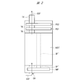
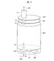
- FIG. 2 and 3 are schematic views showing the entire motor drive system using the electronic apparatus of the present embodiment.
- FIG. 2 shows a side view
- FIG. 3 shows a perspective view, but in FIG. 3, the members that cover the laminate of the power wiring board PB1 and the control wiring board PB2 are: The illustration is omitted.
- the power wiring board PB1 and the control wiring board PB2 are both wiring boards, but the power wiring board PB1 is a wiring board for forming the power system circuit component PK, and is used for control.
- the wiring board PB2 is a wiring board for forming the control system circuit component SK.
- the power wiring board PB1 and the control wiring board PB2 are attached to the motor MOT. Specifically, the power wiring board PB1 and the control wiring board PB2 are attached to the upper part (upper surface) of the motor MOT so as to be stacked in order from the bottom.
- the motor MOT is, for example, a motor for a fuel pump (corresponding to a fuel pump PM described later), and has an impeller (impeller) IMP that rotates together with the shaft SFT.
- the power system circuit component PK is formed by the power wiring board PB1 and the electronic components (not shown in FIGS. 2 and 3) mounted thereon, and the control wiring board PB2 and The control system circuit component SK is formed by electronic components (not shown in FIGS. 2 and 3) mounted thereon.
- the AC power supplied from the power system circuit component PK rotates the shaft SFT of the motor MOT, whereby the impeller IMP fixed to the shaft SFT of the motor MOT is rotated.
- the planar dimensions of the power wiring board PB1 and the control wiring board PB2 are the same as those of the motor MOT. It is desirable that it is equal to or less than the planar dimension.
- the planar shape of the motor MOT is circular, the planar shapes of the power wiring board PB1 and the control wiring board PB2 have the same planar dimension (diameter or area) in accordance with the planar shape of the motor MOT. A circular shape is more preferable because the space can be effectively used without wasting the mounting space.
- a discharge port (tube, pipe) TK for discharging the fuel sucked up by the rotation of the impeller IMP is provided.
- the discharge port TK is a tubular member and is configured to allow fuel to pass through. Through holes are respectively provided in the power wiring board PB1 and the control wiring board PB2 so that the discharge port TK passes therethrough. For this reason, the discharge port TK protrudes above the motor MOT from the upper surface of the motor MOT through the through holes of the power wiring board PB1 and the control wiring board PB2.
- a through hole (corresponding to a hole HT1 described later) through which the discharge port TK in the power wiring board PB1 passes and a through hole (corresponding to a hole HT2 described later) through which the discharge port TK in the control wiring board PB2 passes are in plan view. overlapping.
- the fuel flow GSF sucked up by the rotation of the impeller IMP is schematically shown by arrows. 2 and 3, the fuel sucked up by the rotation of the impeller IMP passes through a space (space) through which the fuel in the motor MOT can pass and is discharged from the motor MOT as indicated by an arrow (GSF). It flows to the outlet TK and is sent from the discharge port TK to the outside of the motor MOT.
- a fuel pipe (not shown) or the like is connected to the discharge port TK, and the fuel sucked up by the rotation of the impeller IMP passes from the motor MOT through the discharge port TK and the fuel tube, which will be described later.
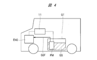
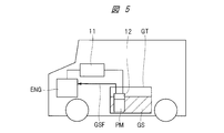
- FIG. 4 and FIG. 5 are explanatory diagrams showing the control system of the automobile.
- FIG. 5 corresponds to the case where the motor drive system shown in FIGS. 1 to 3 is applied to the fuel pump PM. Further, in order to make the drawing easy to see, the fuel GS stored in the fuel tank GT is hatched.
- the fuel GS stored in the fuel tank GT is sucked up by the fuel pump PM and supplied to the engine ENG.
- the flow GSF of the fuel GS sent from the fuel pump PM to the engine ENG through the fuel pipe and the like is schematically shown by arrows.
- the engine ENG is controlled by an ECU (Electronic Control Unit) 11 for engine control.
- the engine control ECU 11 also controls the fuel pump PM. That is, the engine control ECU 11 supplies electric power for driving the motor to the fuel pump PM, thereby driving the motor of the fuel pump PM.
- the engine control ECU 11 controls the motor of the fuel pump PM by controlling the electric power for driving the motor supplied to the fuel pump PM, thereby supplying the engine ENG from the fuel tank GT by the fuel pump PM.
- the amount of fuel GS to be controlled is controlled.
- the fuel pump control ECU 12 attached to the fuel pump PM controls the fuel pump PM.
- the fuel pump control ECU 12 supplies motor driving power to the fuel pump PM, thereby driving the motor of the fuel pump PM.
- the fuel pump control ECU 12 controls the motor of the fuel pump PM by controlling the electric power for driving the motor supplied to the fuel pump PM, and thereby the engine ENG is transmitted from the fuel tank GT by the fuel pump PM. Control the amount of fuel GS supplied.
- a command signal from the engine control ECU 11 to the fuel pump control ECU 12 or a fuel pump control ECU 12
- a feedback signal is transmitted from the ECU 12 to the engine control ECU 11.
- the engine control ECU 11 also serves as the fuel pump control ECU 12, and the fuel pump PM corresponding to the fuel pump control ECU 12 is attached. Absent.
- the fuel pump control ECU 12 is separated from the engine control ECU 11 and attached to the fuel pump PM.
- the engine control ECU 11 also serves as the fuel pump control ECU 12, and the engine control ECU 11 located at a relatively distant position from the fuel pump PM sends a motor to the fuel pump PM. Driving power is supplied. For this reason, power loss will become large. In addition, an increase in weight for wiring arrangement in the automobile, accompanying fuel consumption deterioration, and an increase in necessary space occur.
- the ECU 12 for controlling the fuel pump is attached to the fuel pump PM, and the ECU 12 for controlling the fuel pump is close to the fuel pump PM. Since electric power for driving the motor is supplied to the fuel pump PM from the ECU 12 for fuel pump control attached to the fuel pump PM, power loss can be suppressed. Moreover, the weight increase for wiring arrangement
- the ECU 12 and the fuel pump PM for fuel pump control in the case of FIG. 5 correspond to the motor drive system shown in FIGS. That is, the motor MOT shown in FIGS. 1 to 3 corresponds to the motor of the fuel pump PM.
- the circuit configuration of the ECU 12 for fuel pump control corresponds to the circuit configuration (the power system circuit configuration unit PK and the control system circuit configuration unit SK) other than the motor MOT among the circuit configurations shown in the above figure. Yes. Therefore, the ECU 12 for controlling the fuel pump includes the power wiring board PB1 shown in FIGS. 2 and 3 and the electronic components (not shown in FIGS. 2 and 3) mounted thereon, and the control wiring board PB2. And electronic components (not shown in FIGS. 2 and 3) mounted thereon.
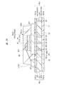
- FIG. 6 is an explanatory view showing the electronic apparatus of the present embodiment attached to the motor MOT.
- FIG. 6 corresponds to a cross-sectional view, but illustration of the internal cross-sectional structure of the motor MOT is omitted.
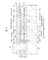
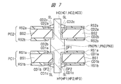
- 7 and 8 are partially enlarged sectional views showing a part of FIG. 6 in an enlarged manner.
- 7 shows a structure for connecting the power wiring board PB1 and the control wiring board PB2 to the connection pins PN (PN1, PN2, PN3)
- FIG. 8 shows the power wiring board PB1.
- a structure for connecting the connection pins BB (BB1, BB2, BB3) is shown.
- the power wiring board PB1 and the control wiring board PB2 are stacked in order from the bottom on the upper surface (upper part) of the motor MOT as shown in FIG. So that it is attached.
- the power wiring board PB1 and the control wiring board PB2 are attached and fixed to the motor MOT by, for example, screws (fixing screws) NG1, and the motor MOT and the power wiring board PB1 And a predetermined gap is interposed between the power wiring board PB1 and the control wiring board PB2.
- the control wiring board PB2 has a hole (through hole) NH2 through which the screw NG1 is inserted, and the power wiring board PB1 also has a screw.
- a hole (through hole) NH1 through which NG1 is inserted is formed.
- a screw hole NH3 for screwing the screw NG1 is formed in the upper part of the motor MOT. Note that the hole NH2 in the control wiring board PB2, the hole NH1 in the power wiring board PB1, and the screw hole NH3 in the motor MOT overlap in plan view.
- the screw NG1 includes the hole NH2 of the control wiring board PB2, the spacer SP2 disposed between the control wiring board PB2 and the power wiring board PB1, the hole NH1 of the power wiring board PB1, and the power A spacer SP1 disposed between the wiring board PB1 and the upper surface of the motor MOT is inserted and screwed into the screw hole NH3 of the motor MOT.
- the spacer SP1 secures a predetermined distance between the motor MOT and the power wiring board PB1
- the spacer SP2 secures a predetermined distance between the power wiring board PB1 and the control wiring board PB2.
- the control wiring board PB2 and the power wiring board PB1 are attached and fixed to the upper surface (upper part) of the motor MOT by screws NG1. Although only one screw NG1 is shown in FIG. 6 as a representative, the screw NG1 is used to fix the control wiring board PB2 and the power wiring board PB1 to the motor MOT, as will be described later. Three are used
- a protective cover member (case, casing) CV is provided so as to cover the power wiring board PB1 and the control wiring board PB2 attached to the upper part of the motor MOT. You can also.
- This cover member CV is fixed to the motor MOT.
- the cover member CV may be a separate member from the motor MOT or may be an integral member with the motor MOT.
- the power wiring board PB1 (wiring) and the control wiring board PB2 (wiring) are electrically connected by a plurality of connection pins PN.
- the connection pins PN that electrically connect the power wiring board PB1 (wiring) and the control wiring board PB2 (wiring) include a power connection pin PN1, a ground connection pin PN2, and a signal pin PN3.
- connection pins PN connection pins
- the control wiring board PB2 has a plurality of holes (through holes) HC through which the connection pins PN are inserted, and the power wiring board PB1 has a plurality of holes (through the connection pins PN).
- Through holes) HP are formed.
- FIG. 7 representatively shows a pair of holes HC, HP and one connection pin PN inserted therethrough.
- the diameter of the signal pin PN3 is smaller than the diameters of the power supply connection pin PN1 and the ground connection pin PN2.
- connection pin PN is made of a conductor and preferably made of a metal material.
- each connection pin PN the part located in the hole HC of the control wiring board PB2 has a diameter slightly smaller than the diameter of the hole HC, and the part located in the hole HP of the power wiring board PB1 is the hole HP. It has a diameter slightly smaller than the diameter.
- the part located outside the holes HC and HP and between the power wiring board PB1 and the control wiring board PB2 is larger than the diameters of the holes HP and HC. It can also have a diameter, whereby the height positions of the power wiring board PB1 and the control wiring board PB2 with respect to the connection pin PN can be positioned.
- the control wiring board PB2 and the power wiring board PB1 are, for example, resin boards.
- the control wiring board PB2 includes an insulating base material layer BS2, a wiring pattern (conductive film CD2a) formed on the upper surface of the base material layer BS2, and a wiring pattern (on the lower surface of the base material layer BS2).
- the power wiring board PB1 includes an insulating base material layer BS1, a wiring pattern (conductive film CD1a) formed on the upper surface of the base material layer BS1, and a wiring formed on the lower surface of the base material layer BS1.
- the base material layers BS1 and BS2 are made of an insulating material (insulating layer), for example, glass epoxy resin.
- the wiring pattern on the upper surface of the control wiring board PB2 is formed by the conductive film CD2a
- the wiring pattern on the lower surface of the control wiring board PB2 is formed by the conductive film CD2b
- the wiring pattern on the upper surface of the power wiring board PB1 is
- the wiring pattern formed of the conductive film CD1a and the lower surface of the power wiring board PB1 is formed of the conductive film CD1b.
- Each of the resist layers RS1a, RS1b, RS2a, RS2b is made of an insulating material (insulating layer), for example, a solder resist layer.
- the resist layers RS1a, RS1b, RS2a, RS2b can also be regarded as protective films.
- a conductive film CD2c is formed on the side surface (inner wall) of the hole HC, and in the power wiring board PB1, a conductive film CD1c is formed on the side surface (inner wall) of the hole HP.
- the conductive film CD2c on the side surface of the hole HC of the control wiring board PB2 is electrically connected to the connection pin PN inserted through the hole HC, and the conductive film CD1c on the side surface of the hole HP of the power wiring board PB1 is The connection pin PN inserted through the hole HC is electrically connected.
- a conductive bonding material such as solder SL is interposed between the conductive film CD2c on the side surface of the hole HC of the control wiring board PB2 and the connection pin PN, and is electrically connected via the conductive bonding material.
- a conductive bonding material such as solder SL is interposed between the conductive film CD1c on the side surface of the hole HP of the power wiring board PB1 and the connection pin PN, and the conductive bonding material such as the solder SL is electrically interposed therebetween. Connected.
- the conductive film CD2c on the side surface of the hole HC of the control wiring board PB2 and the connection pin PN may be electrically connected to each other, and the side surface of the hole HP of the power wiring board PB1 may be connected.
- the conductive film CD1c and the connection pin PN may be electrically connected by being in contact with each other.
- connection pins PN can also be fixed to the control wiring board PB2 and the power wiring board PB1 using a conductive bonding material such as solder SL.
- the conductive film CD1c on the side surface of the hole HP of the power wiring board PB1 is electrically connected to the conductive film CD1a formed around the hole HP on the upper surface of the power wiring board PB1, and the power wiring board PB1. Is electrically connected to the conductive film CD1b formed around the hole HP.
- the conductive film CD2c on the side surface of the hole HC of the control wiring board PB2 is electrically connected to the conductive film CD2a formed around the hole HC on the upper surface of the control wiring board PB2, and the control wiring
- the lower surface of the substrate PB2 is electrically connected to the conductive film CD2b formed around the hole HC. Accordingly, in FIG.
- the conductive films CD1a, CD1b, CD1c of the power wiring board PB1 and the conductive films CD2a, CD2b, CD2c of the control wiring board PB2 can be electrically connected via the connection pins PN. it can.
- a part of the wiring pattern is used.
- a conductive film CD2c provided around the hole HC and electrically connected to the wiring pattern is formed on the side surface of the hole HC, and the connection pin PN is inserted into the hole HC. Then, if necessary, the connection pin PN is joined to the control wiring board PB2 with a conductive joining material such as solder SL. Thereby, the wiring pattern formed on the upper surface or the lower surface of the control wiring board PB2 can be electrically connected to the connection pin PN.
- a part of the wiring pattern is used.
- a conductive film CD1c provided around the hole HP and electrically connected to the wiring pattern is formed on the side surface of the hole HP, and the connection pin PN is inserted into the hole HP. Then, if necessary, the connection pin PN is bonded to the power wiring board PB1 with a conductive bonding material such as solder SL. Thereby, the wiring pattern formed on the upper surface or the lower surface of the power wiring board PB1 can be electrically connected to the connection pin PN.
- the resist layers RS2a and RS2b may have an opening that encloses the hole HC in plan view.
- one or both of the conductive films CD2a and CD2b exposed from the openings of the resist layers RS2a and RS2b around the hole HC of the control wiring board PB2 is connected to the connection pin PN via a conductive bonding material such as solder SL. It can also be electrically connected.
- the resist layers RS1a and RS1b may have openings OP1 and OP2 that enclose the holes HP in a plan view.
- the opening OP1 is an opening of the resist layer RS1a on the upper surface side of the power wiring board PB1
- the opening OP2 is an opening of the resist layer RS1b on the lower surface side of the power wiring board PB1.
- one or both of the conductive films CD1a and CD1b exposed from the openings OP1 and OP2 of the resist layers RS1a and RS1b around the hole HP of the power wiring board PB1 are interposed via a conductive bonding material such as solder SL. It can also be electrically connected to the connection pin PN.
- the conductive film CD1b) can be electrically connected via the connection pin PN.
- the power supply potential VIN and the ground potential GND are supplied to both the power wiring board PB1 and the control wiring board PB2.
- the power supply potential VIN and the ground potential GND are supplied from the battery (not shown) or the like to the control wiring board PB2 via the cable CB, respectively, and the power supply potential VIN supplied to the control wiring board PB2 is supplied.
- the ground potential GND are supplied to the power wiring board PB1 via the power connection pin PN1 and the ground connection pin PN2, respectively.
- the power supply connection pin PN1 is a connection pin PN used to supply the power supply potential VIN from the control wiring board PB2 to the power wiring board PB1.
- the ground connection pin PN2 is a connection pin PN used to supply the ground potential GND from the control wiring board PB2 to the power wiring board PB1.
- FIG. 6 only one cable CB is shown for simplification, but in reality, there are two cables CB, one is a cable CB for supplying a power supply potential VIN, and the other is a cable CB. , A cable CB for supplying a ground potential GND.
- the power supply potential VIN supply cable CB and the ground potential GND supply cable CB are not electrically connected but are separate members.
- the power connection pin PN1 and the ground connection pin PN2 are represented by one connection pin PN, but in reality, one power connection pin PN1 is shown. And one ground connection pin PN2, and the power connection pin PN1 and the ground connection pin PN2 are not electrically connected but are separate members.
- the power supply potential VIN supply cable CB is fixed to the control wiring board PB2 with screws NG2 or the like, whereby the power supply potential VIN supply cable CB is It is electrically connected to the power supply wiring of the control wiring board PB2.
- the power supply potential VIN is supplied from the power supply potential VIN supply cable CB to the power supply wiring of the control wiring board PB2.
- the ground potential GND supply cable CB is fixed to the control wiring board PB2 with screws NG2 or the like, whereby the ground potential GND supply cable CB is electrically connected to the ground wiring of the control wiring board PB2. It is connected.
- the ground potential GND is supplied from the ground potential GND supply cable CB to the ground wiring of the control wiring board PB2.
- the power wiring of the control wiring board PB2 is electrically connected to the power wiring of the power wiring board PB1 (corresponding to power wirings WV1 and WV2 described later) via the power connection pin PN1.
- the control wiring board PB2 has a hole (through hole) HC1 through which the power connection pin PN1 is inserted
- the power wiring board PB1 has a hole (through hole) through which the power connection pin PN1 is inserted. It has HP1.
- the power supply wiring of the control wiring board PB2, the power supply wiring of the power wiring board PB1, and the power supply wiring of the power wiring board PB1 by the power connection pin PN1 inserted through the hole HC1 of the control wiring board PB2 and the hole HP1 of the power wiring board PB1 are electrically connected.
- the connection pin PN in FIG. 7 corresponds to the power supply connection pin PN1
- the hole HC in FIG. 7 corresponds to the hole HC1
- the hole HP in FIG. 7 corresponds to the hole HP1.
- the conductive films CD2a and CD2b in FIG. 7 correspond to the power supply wirings of the control wiring board PB2
- the conductive films CD1a and CD1b in FIG. 7 correspond to the power supply wirings (power supply wirings WV1 and WV2 described later) of the power wiring board PB1.
- the connection pin PN in FIG. 7 corresponds to the power supply connection pin PN1
- the hole HC in FIG. 7 corresponds to the hole HC1
- the ground wiring of the control wiring board PB2 is electrically connected to the ground wiring (corresponding to ground wirings WG1 and WG2 described later) of the power wiring board PB1 through the ground connection pin PN2. That is, the control wiring board PB2 has a hole (through hole) HC2 through which the ground connection pin PN2 is inserted, and the power wiring board PB1 has a hole (through hole) HP2 through which the ground connection pin PN2 is inserted. is doing.
- the connection pin PN in FIG. 7 corresponds to the ground connection pin PN2
- the hole HC in FIG. 7 corresponds to the hole HC2
- the hole HP in FIG. 7 corresponds to the hole HP2.
- the conductive films CD2a and CD2b in FIG. 7 correspond to the ground wiring of the control wiring board PB2
- the conductive films CD1a and CD1b in FIG. 7 correspond to the ground wiring (ground wirings WG1 and WG2 described later) of the power wiring board PB1. Correspond.
- the power supply potential VIN supplied to the power supply wiring of the control wiring board PB2 through the power supply potential VIN supply cable CB is supplied to the power supply wiring board PB1 through the power supply connection pin PN1.
- the power supply potential VIN is supplied from the power supply connection pin PN1 to the power supply wiring (power supply wirings WV1, WV2 described later) of the power wiring board PB1.
- the ground potential GND supplied to the ground wiring of the control wiring board PB2 via the ground potential GND supply cable CB is supplied to the ground wiring (PW1) of the power wiring board PB1 via the ground connection pin PN2. It is supplied to ground wirings WG1 and WG2) to be described later. That is, the ground potential GND is supplied from the ground connection pin PN2 to the ground wiring (ground wirings WG1 and WG2 described later) of the power wiring board PB1.
- the power wiring board PB1 (signal wiring thereof) and the control wiring board PB2 (signal wiring thereof) are electrically connected via a plurality of signal pins PN3.
- the signal pin PN3 is a connection pin used to electrically connect the power system circuit configuration unit PK and the control circuit unit CT (see FIG. 1 above). A signal or the like can be transmitted between the control circuit unit CT and the power system circuit configuration unit PK via the signal pin PN3.
- the control wiring board PB2 has a hole (through hole) HC3 through which the signal pin PN3 is inserted
- the power wiring board PB1 has a hole (through hole) HP3 through which the signal pin PN3 is inserted.
- the signal wiring PN3 inserted into the hole HC3 of the control wiring board PB2 and the hole HP3 of the power wiring board PB1 makes the signal wiring of the control wiring board PB2 and the signal wiring of the power wiring board PB1.
- the connection pin PN in FIG. 7 corresponds to the signal pin PN3
- the hole HC in FIG. 7 corresponds to the hole HC3
- the hole HP in FIG. 7 corresponds to the hole HP3.
- the conductive films CD2a and CD2b in FIG. 7 correspond to the signal wiring of the control wiring board PB2, and the conductive films CD1a and CD1b in FIG. 7 correspond to the signal wiring of the power wiring board PB1.
- the signal wiring on the control wiring board PB2 and the signal wiring on the power wiring board PB1 are wirings for connecting the power system circuit component PK to the control circuit part CT.
- a plurality of signal pins PN3 are provided.
- the signal pin PN3 includes two signal pins PN3 respectively connected to both ends of the resistor R1, two signal pins PN3 respectively connected to both ends of the resistor R4, and the resistor R7. And two signal pins PN3 respectively connected to both ends.
- the signal pin PN3 is further electrically connected to the gate of the power MOSFET 1 via the resistor R2, and the signal pin PN3 is electrically connected to the gate of the power MOSFET 2 via the resistor R3.
- a signal pin PN3 and a signal pin PN3 electrically connected to the gate of the power MOSFET 3 via the resistor R5 are also included.
- the signal pin PN3 is further electrically connected to the gate of the power MOSFET 4 via the resistor R6 and the signal pin PN3 electrically connected to the gate of the power MOSFET 5 via the resistor R8.
- a signal pin PN3 and a signal pin PN3 electrically connected to the gate of the power MOSFET 6 via the resistor R9 are also included.
- the signal pin PN3 may further include six signal pins PN3 connected to the sources of the power MOSFETs 1, 2, 3, 4, 5, and 6, respectively.
- the gates of the power MOSFETs 1, 2, 3, 4, 5, and 6 are connected to signal wirings and resistance elements of the power wiring board PB1 (any one of the resistors R2, R3, R5, R6, R8, R9).
- both ends of the resistors R1, R4, and R7 are electrically connected to the signal pin PN3 through the signal wiring of the power wiring board PB1, respectively, and the signal pin PN3 and the control wiring board PB2 are further connected.
- Each source of the power MOSFETs 1, 2, 3, 4, 5, 6 is electrically connected to the signal pin PN3 via the signal wiring of the power wiring board PB1, and further, the signal pin PN3 It is electrically connected to the electronic components constituting the control circuit unit CT via the signal wiring of the control wiring board PB2.
- the electronic component constituting the control circuit unit CT is an electronic component mounted on the control wiring board PB2, and for example, a semiconductor device (semiconductor package) incorporating a semiconductor chip can be exemplified.
- connection pins BB (BB1, BB2, BB3)
- connection pins BB (BB1, BB2, BB3).
- the connection pin (bus bar) BB that electrically connects the power wiring board PB1 (wiring thereof) and the motor MOT includes the connection pin BB1, the connection pin BB2, and the connection pin BB3.
- a representative connection pin BB is shown.
- the connection pin BB1, the connection pin BB2, and the connection pin BB3 are not electrically connected but are separate members.
- the power wiring board PB1 has holes (through holes) HM1, HM2, and HM3 through which the connection pins BB1, BB2, and BB3 are inserted, respectively.
- connection pin BB corresponds to the connection pin BB1
- connection pin BB corresponds to the connection pin BB2.
- connection pin PN electrically connects the power wiring board PB1 (wiring) and the control wiring board PB2 (wiring), but the connection pin BB is connected to the connection pin PN.
- the power wiring board PB1 and the control wiring board PB2 are not electrically connected, but the power wiring board PB1 (wiring thereof) and the motor MOT (coil thereof) are electrically connected. is there.
- the connection pin BB is also made of a conductor, preferably a metal material.
- the power wiring board PB1 has a hole (through hole) HM1 through which the connection pin BB1 is inserted, a hole (through hole) HM2 through which the connection pin BB2 is inserted, and a hole (through hole) through which the connection pin BB3 is inserted. Hole) HM3. Then, one end side of the connection pin BB1 is inserted into the hole HM1 of the power wiring board PB1, and the other end side of the connection pin BB1 is inserted into and fixed to the upper hole of the motor MOT.
- connection pin BB2 is inserted into the hole HM2 of the power wiring board PB1, and the other end side of the connection pin BB2 is inserted into the upper hole of the motor MOT and fixed.
- connection pin BB3 is inserted into the hole HM3 of the power wiring board PB1, and the other end side of the connection pin BB3 is inserted into and fixed to the upper hole of the motor MOT.
- the connection pin BB1 is electrically connected to a U-phase coil in the motor MOT via an internal wiring (not shown) of the motor MOT
- the connection pin BB2 is an internal wiring (not shown) of the motor MOT. Is electrically connected to the V-phase coil in the motor MOT
- connection pin BB3 is electrically connected to the W-phase coil in the motor MOT via an internal wiring (not shown) of the motor MOT.
- connection pins BB1, BB2, and BB3 will be described with reference to FIG.
- a conductive film CD1c is formed on the side surface (inner wall) of the hole HM, and the conductive film CD1c on the side surface of the hole HM is inserted into the hole HM.
- the connection pin BB is electrically connected.
- a conductive bonding material such as solder SL is interposed between the conductive film CD1c on the side surface of the hole HM of the power wiring board PB1 and the connection pin BB inserted through the hole HM. Electrically connected.
- the conductive film CD1c on the side surface of the hole HM of the power wiring board PB1 and the connection pin BB inserted through the hole HM may be electrically connected by contacting each other.
- the connection pin BB can also be fixed to the power wiring board PB1 using a conductive bonding material such as solder SL.
- the conductive film CD1c on the side surface of the hole HM of the power wiring board PB1 is electrically connected to the conductive film CD1a formed around the hole HM on the upper surface of the power wiring board PB1, and the power wiring board PB1. Is electrically connected to the conductive film CD1b formed around the hole HM. Therefore, in FIG. 8, the conductive films CD1a, CD1b, CD1c of the power wiring board PB1 can be electrically connected to the connection pins BB.
- the wiring pattern (conductive film CD1a or conductive film CD1b) formed on the upper surface or the lower surface of the power wiring board PB1 can be electrically connected to the connection pin BB.
- the resist layers RS1a and RS1b may have openings OP1 and OP2 that enclose the holes HM in a plan view.
- one or both of the conductive films CD1a and CD1b exposed from the openings OP1 and OP2 of the resist layers RS1a and RS1b around the hole HM of the power wiring board PB1 are interposed via a conductive bonding material such as solder SL. It can also be electrically connected to the connection pin BB.
- output wirings WD1 and WD4 which will be described later, of the power wiring board PB1 are electrically connected to a connection pin BB1 that passes through the hole HM1, and via the connection pin BB1 and an internal wiring (not shown) of the motor MOT. Are electrically connected to the U-phase coil in the motor MOT. Further, output wirings WD2 and WD5 described later of the power wiring board PB1 are electrically connected to a connection pin BB2 inserted through the hole HM2, and via the connection pin BB2 and an internal wiring (not shown) of the motor MOT. And electrically connected to a V-phase coil in the motor MOT.
- output wirings WD3 and WD6 described later of the power wiring board PB1 are electrically connected to a connection pin BB3 that is inserted through the hole HM3, and via the connection pin BB3 and an internal wiring (not shown) of the motor MOT. And electrically connected to a W-phase coil in the motor MOT.
- the discharge port TK protruding from the motor MOT passes through the hole (through hole) HT1 of the power wiring board PB1 and the hole (through hole) HT2 of the control wiring board PB2. Yes.
- the fuel (not shown) sucked up by the motor MOT is supplied to the engine ENG (not shown in FIG. 6) through the discharge port TK and a fuel pipe (not shown in FIG. 6) connected thereto. .
- the electronic component (EC2) mounted on the control wiring board PB2 is typically a semiconductor device (semiconductor package) incorporating a semiconductor chip, but in addition, an electronic component other than the semiconductor device (semiconductor package) (For example, passive components such as chip resistors) may be mounted on the control wiring board PB2.
- Each electronic component (EC2) mounted on the control wiring board PB2 is electrically connected to the wiring of the control wiring board PB2, and is connected to each other as necessary by the wiring of the control wiring board PB2. Yes.
- Each electronic component (EC2) mounted on the control wiring board PB2 includes a power supply potential VIN supply cable CB, a ground potential GND supply cable CB, the power supply connection pin PN1, and the ground connection. It is electrically connected to the signal pin PN2 or the signal pin PN3 through the wiring of the control wiring board PB2 as necessary.
- ⁇ Mounting structure on power wiring board> On the power wiring board PB1, a plurality of electronic components for forming the power system circuit component PK are mounted. In FIG. 6, these electronic components are represented as electronic components EC1. Yes. Each electronic component (EC1) mounted on the power wiring board PB1 is electrically connected to the wiring of the power wiring board PB1.
- FIG. 9 is a top view of the power wiring board PB1, and also shows a plurality of electronic components (EC1) mounted on the power wiring board PB1. Specifically, semiconductor devices (semiconductor packages) PKG1, PKG2, and PKG3 and chip resistors R1a, R2a, R3a, R4a, R5a, R6a, R7a, R8a, and R9a are provided on the upper surface of the power wiring board PB1. Mounted.
- semiconductor devices semiconductor packages
- PKG1, PKG2, and PKG3 and chip resistors R1a, R2a, R3a, R4a, R5a, R6a, R7a, R8a, and R9a are provided on the upper surface of the power wiring board PB1. Mounted.
- the semiconductor device PKG1 is a semiconductor device that constitutes the power MOSFET 1 and the power MOSFET 2.
- the semiconductor device PKG2 is a semiconductor device that constitutes the power MOSFET 3 and the power MOSFET 4.
- the semiconductor device PKG3 includes the power MOSFET 5 and the power MOSFET 4. This is a semiconductor device constituting the power MOSFET 6.
- the chip resistor R1a is a resistor element constituting the resistor R1
- the chip resistor R2a is a resistor element constituting the resistor R2
- the chip resistor R3a is a resistor element constituting the resistor R3
- the chip resistor R4a is a resistance element constituting the resistor R4.
- the chip resistor R5a is a resistor element that constitutes the resistor R5
- the chip resistor R6a is a resistor element that constitutes the resistor R6
- the chip resistor R7a is a resistor element that constitutes the resistor R7.
- the chip resistor R8a is a resistor element that constitutes the resistor R8, and the chip resistor R9a is a resistor element that constitutes the resistor R9.
- the semiconductor devices PKG1, PKG2, and PKG3 generate a large amount of heat during operation. For this reason, at a position overlapping each of the semiconductor devices PKG1, PKG2, and PKG3 in plan view, that is, at a position directly below each of the semiconductor devices PKG1, PKG2, and PKG3, the lower surface of the power wiring board PB1 and the upper surface of the motor MOT A heat radiating member such as the heat radiating sheet HS (see FIG. 6) can be interposed (arranged) between the two.
- the heat generated in the semiconductor devices PKG1, PKG2, and PKG3 can be efficiently conducted (heat radiation) to the motor MOT via the power wiring board PB1 and the heat radiation sheet HS.
- the heat dissipation characteristics of the semiconductor devices PKG1, PKG2, and PKG3 can be improved, and thereby the performance of the electronic device can be further stabilized and improved.
- the structure of the semiconductor device PKG1, the structure of the semiconductor device PKG2, and the structure of the semiconductor device PKG3 are basically the same.
- Each of the semiconductor devices PKG1, PKG2, and PKG3 incorporates two semiconductor chips.
- One of the two semiconductor chips built in the semiconductor device PKG1 constitutes the power MOSFET 1, and the other constitutes the power MOSFET 2.
- One of the two semiconductor chips built in the semiconductor device PKG2 constitutes the power MOSFET 3, and the other constitutes the power MOSFET 4.
- One of the two semiconductor chips built in the semiconductor device PKG3 constitutes the power MOSFET 5, and the other constitutes the power MOSFET 6.
- the configuration of the semiconductor device PKG1 Since the configuration of the semiconductor device PKG1, the configuration of the semiconductor device PKG2, and the configuration of the semiconductor device PKG3 are basically the same, here, as a representative example, the configuration of the semiconductor device PKG1 will be described with reference to FIGS. The description will be given with reference.
- FIG. 10 is a top view of the semiconductor device PKG1
- FIG. 11 is a bottom view of the semiconductor device PKG1.
- FIG. 12 is a plan perspective view of the semiconductor device PKG1, and a plan perspective view of the upper surface side of the semiconductor device PKG1 when the sealing portion MR is seen through is shown.
- the outer peripheral position of the sealing portion MR is indicated by a dotted line.
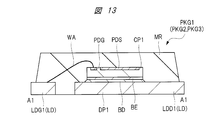
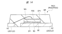
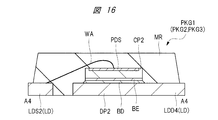
- 13 to 16 are cross-sectional views of the semiconductor device PKG1.
- 13 substantially corresponds to the sectional view taken along the line A1-A1 in FIG. 12
- FIG. 14 substantially corresponds to the sectional view taken along the line A2-A2 in FIG. 12
- FIG. 15 corresponds to the sectional view taken along the line A3-A3 in FIG.
- FIG. 16 substantially corresponds to the sectional view taken along the line A4-A4 of FIG.
- the semiconductor device PKG1 includes die pads (chip mounting portions) DP1 and DP2, semiconductor chips CP1 and CP2 mounted on the upper surfaces of the die pads DP1 and DP2, and a plurality of semiconductor devices CPKG1 and DP2. It has a bonding wire (hereinafter simply referred to as a wire) WA, a plurality of leads LD, and a sealing portion (sealing resin portion, sealing body) MR for sealing them.
- a bonding wire hereinafter simply referred to as a wire
- LD bonding wire
- sealing portion sealing resin portion, sealing body
- the sealing portion MR as the sealing body is made of a resin material such as a thermosetting resin material, and can include a filler.
- the semiconductor device PKG1 is a surface-mounting type semiconductor package.
- the semiconductor device PKG1 is a HSON (Small Outline No Lead Package with Heat Sink) type surface mount type semiconductor package.
- the configuration of the semiconductor device PKG1 is not limited to this, and can be variously changed.
- the die pad DP1 and the die pad DP2 are arranged side by side in a plan view.
- the semiconductor chip CP1 is mounted on the die pad DP1, and the semiconductor chip CP2 is mounted on the die pad DP2.
- a power MOSFET is formed on the semiconductor chip CP1. Specifically, a large number of unit transistor cells are formed on a semiconductor substrate constituting the semiconductor chip CP1, and a power MOSFET is formed by connecting the large number of unit transistor cells in parallel.
- the unit transistor cell is constituted by, for example, a trench gate type field effect transistor.
- a source pad (source bonding pad, source electrode) PDS connected to the source of the power MOSFET and a gate pad (gate bonding pad, gate) connected to the gate of the power MOSFET Electrode) PDG is formed.
- a back surface electrode (back surface drain electrode, drain electrode) BE connected to the drain of the power MOSFET is formed on the entire back surface of the semiconductor chip CP1.
- the source pad PDS can be regarded as a source electrode (source electrode)
- the gate pad PDG can be regarded as a gate electrode (gate electrode)
- the back electrode BE can be regarded as a drain electrode. .
- the back electrode BE of the semiconductor chip CP1 is bonded to the upper surface of the die pad DP1 via a conductive bonding material BD, and the back electrode BE of the semiconductor chip CP2 is bonded to the upper surface of the die pad DP2 via a conductive bonding material BD.
- the back surface electrode BE of the semiconductor chip CP1 is electrically connected to the die pad DP1
- the back surface electrode BE of the semiconductor chip CP2 is electrically connected to the die pad DP2.
- the plurality of leads LD included in the semiconductor device PKG1 includes gate leads LDG1, LDG2, source leads LDS1, LDS2, and drain leads LDD1, LDD2, LDD3, LDD4.
- the gate lead LDG1 is electrically connected to the gate pad PDG of the semiconductor chip CP1 via the wire WA.
- the gate lead LDG2 is electrically connected to the gate pad PDG of the semiconductor chip CP2 via the wire WA.
- the source lead LDS1 is electrically connected to the source pad PDS of the semiconductor chip CP1 via the wire WA.
- the source lead LDS2 is electrically connected to the source pad PDS of the semiconductor chip CP2 via the wire WA.
- the semiconductor chip CP1 is a high-side semiconductor chip including a high-side MOSFET (any one of the power MOSFETs 1, 3 and 5), and the semiconductor chip CP2 is a low-side MOSFET (any one of the power MOSFETs 2, 4 and 6).
- a semiconductor chip for low side For this reason, the source lead LDS1 electrically connected to the source pad PDS of the semiconductor chip CP1 can be regarded as a high-side source terminal, and is electrically connected to the source pad PDS of the semiconductor chip CP2.
- the source lead LDS2 can be regarded as a low-side source terminal.
- the gate lead LDG1 electrically connected to the gate pad PDG of the semiconductor chip CP1 can be regarded as a high-side gate terminal, and the gate electrically connected to the gate pad PDG of the semiconductor chip CP2.
- the lead LDG2 can be regarded as a low-side gate terminal.
- the die pad DP1 (and drain leads LDD1, LDD2) electrically connected to the back electrode BE of the semiconductor chip CP1 can be regarded as a high side drain terminal, and is electrically connected to the back electrode BE of the semiconductor chip CP2.
- the die pad DP2 (and the drain leads LDD3 and LDD4) connected to can be regarded as a low-side drain terminal.
- FIG. 12 shows a case where the source lead LDS1 and the source pad PDS of the semiconductor chip CP1 are connected by a single wire WA.
- the source lead LDS1 and the source pad PDS of the semiconductor chip CP1 may be connected by a plurality of wires WA, and the source lead LDS1 and the source of the semiconductor chip CP1 may be connected.
- the pad PDS for use may be connected by a metal plate instead of the wire WA. The same applies to the connection between the source lead LDS2 and the source pad PDS of the semiconductor chip CP2.
- drain lead LDD1 and the drain lead LDD2 are formed integrally with the die pad DP1, not only the die pad DP1, but also the drain lead LDD1 and the drain lead LDD2 are electrically connected to the back electrode BE of the semiconductor chip CP1. It is connected to the. Further, since the drain lead LDD3 and the drain lead LDD4 are formed integrally with the die pad DP2, not only the die pad DP2, but also the drain lead LDD3 and the drain lead LDD4 are connected to the back surface electrode BE of the semiconductor chip CP2. Electrically connected.
- the drain leads LDD1 and LDD2 can be regarded as a part of the die pad DP1, and the drain leads LDD3 and LDD4 can be regarded as a part of the die pad DP2.
- the gate lead LDG1 and the source lead LDS1 are arranged at a position separated from the die pad DP1 in the Y direction, and the gate lead LDG2 and the source lead LDS2 are arranged at a position separated from the die pad DP2 in the Y direction.
- a drain lead LDD1 and a drain lead LDD2 are formed integrally with the die pad DP1 on the side opposite to the side where the gate lead LDG1 and the source lead LDS1 are arranged. Further, on the side opposite to the side where the gate lead LDG2 and the source lead LDS2 are disposed, the drain lead LDD3 and the drain lead LDD4 are formed integrally with the die pad DP2.
- the die pad DP1 and the die pad DP2 are arranged in the X direction.
- the gate lead LDG1, the source lead LDS1, the gate lead LDG2, and the source lead LDS2 are arranged in this order in the X direction.
- the drain lead LDD1, the drain lead LDD2, the drain lead LDD3, and the drain lead LDD4 are arranged in this order in the X direction.
- the X direction and the Y direction are directions intersecting each other, and preferably are directions orthogonal to each other.
- the planar shape of the sealing portion MR is substantially rectangular, and the sides (side surfaces) SD1 and SD3 parallel to the Y direction and facing the X direction, and the sides (side surfaces) SD2 parallel to the X direction and facing the Y direction. , SD4.
- the gate lead LDG1, the source lead LDS1, the gate lead LDG2, and the source lead LDS2 are arranged on the side SD2 side.
- the drain lead LDD1, the drain lead LDD2, the drain lead LDD3, and the drain lead LDD4 Are arranged on the side SD4 side.
- the die pads DP1, DP2, gate leads LDG1, LDG2, source leads LDS1, LDS2 and drain leads LDD1, LDD2, LDD3, LDD4 are sealed by a sealing portion MR.
- the lower surfaces of the die pads DP1, DP2, gate leads LDG1, LDG2, source leads LDS1, LDS2 and drain leads LDD1, LDD2, LDD3, LDD4 are exposed from the lower surface of the sealing portion MR, and the semiconductor device PKG1. External connection terminal.
- the die pad DP1, the die pad DP2, the gate lead LDG1, the source lead LDS1, the gate lead LDG2, and the source lead LDS2 are separated from each other, and a part of the sealing portion MR is interposed therebetween.
- FIG. 17 shows a top view of the power wiring board PB1.
- the electronic components specifically, the semiconductor devices PKG1, PKG2, PKG3 and chip resistors R1a, R2a, R3a, R4a, R5a, R6a, R7a, R8a, R9a mounted on the power wiring board PB1.
- FIG. 17 corresponds to FIG.
- FIG. 18 is a plan perspective view of the power wiring board PB1.
- FIG. 18 shows a plan view (plan view) of the upper surface side of the power wiring board PB1 when the resist layer RS1a on the upper surface side of the power wiring board PB1 is seen through. That is, in FIG. 17, the perspective view of the resist layer RS1a on the upper surface side of the power wiring board PB1 corresponds to FIG. Accordingly, FIG. 18 shows a wiring pattern on the upper surface side of the power wiring board PB1 (a wiring pattern on the upper surface of the base material layer BS1, that is, a wiring pattern formed by the conductive film CD1a). For simplicity, the wiring pattern on the upper surface side of the power wiring board PB1 is hatched although it is a plan view. Further, in FIG.
- FIG. 19 is a plan perspective view of the lower surface side of the power wiring board PB1
- FIG. 20 is a bottom view of the power wiring board PB1. That is, in FIG. 20, the perspective view of the resist layer RS1b on the lower surface side of the power wiring board PB1 corresponds to FIG. Accordingly, FIG. 19 shows a wiring pattern on the lower surface side of the power wiring board PB1 (a wiring pattern on the lower surface of the base material layer BS1, that is, a wiring pattern formed by the conductive film CD1b).
- the wiring pattern on the lower surface side of the power wiring board PB1 is hatched although it is a plan view.
- the main surface facing the motor MOT corresponds to the lower surface of the power wiring board PB1
- the main surface facing the control wiring board PB2 is the upper surface of the power wiring board PB1. It corresponds to.
- the main surface on the side facing the power wiring board PB1 corresponds to the lower surface of the control wiring board PB2.
- the power wiring board PB1 has a circular planar shape.
- a wiring pattern is formed on each of the upper and lower surfaces of the power wiring board PB1. Then, on the upper surface of the power wiring board PB1, the semiconductor device PKG1, the semiconductor device PKG2, the semiconductor device PKG3, the chip resistor R1a, the chip resistor R2a, the chip resistor R3a, the chip resistor R4a, and the chip resistor R5a
- the chip resistor R6a, the chip resistor R7a, the chip resistor R8a, and the chip resistor R9a are mounted at different positions (planar positions).
- the power supply wiring (conductor pattern) WV1, the ground wiring (conductor pattern) WG1, the output wiring (conductor pattern) WD1, WD2, WD3, and the signal wiring ( Conductor pattern) WS is formed on the upper surface of the power wiring board PB1.
- power supply wiring (conductor pattern) WV2, ground wiring (conductor pattern) WG2, and output wiring (conductor pattern) WD4, WD5, WD6 are formed.
- No equivalent of the signal wiring WS is formed on the lower surface of the power wiring board PB1.
- the wiring on the upper surface of the power wiring board PB1 (that is, the power wiring WV1, the ground wiring WG1, the output wiring WD1, WD2, WD3, and the signal wiring WS) is on the upper surface of the base material layer BS1 constituting the power wiring board PB1. Formed by the conductive film (corresponding to the conductive film CD1a). Further, the wiring on the lower surface of the power wiring board PB1 (that is, the power wiring WV2, the ground wiring WG2, and the output wirings WD4, WD5, WD6) is formed on the lower surface of the base material layer BS1 constituting the power wiring board PB1. The conductive film (corresponding to the conductive film CD1b) is formed.
- the power supply wiring WV1, the ground wiring WG1, the output wirings WD1, WD2, and WD3, the signal wiring WS, the power supply wiring WV2, the ground wiring WG2, and the output wirings WD4, WD5, and WD6 can all be regarded as conductor patterns.
- the power supply wiring WV1 and the power supply wiring WV2 are lines to which the power supply potential VIN is supplied.
- the power supply wiring WV1 and the power supply wiring WV2 are electrically connected to the power supply connection pin PN1 inserted through the hole HP1 of the power wiring board PB1, and the power supply wiring WV1 and the power supply wiring WV2 are connected to the power supply connection pin PN1. Is supplied with a power supply potential VIN.
- the hole HP1 for inserting the power connection pin PN1 is provided at a position included in both the power wirings WV1 and WV2 in a plan view.
- a conductive film (CD1c) electrically connected to the power supply lines WV1 and WV2 is formed on the side surface of the hole HP1, and the power connection pin PN1 is inserted into the hole HP1.
- the power connection pin PN1 is joined to the power wiring board PB1 with a conductive joining material such as solder (SL).
- SL solder
- connection pin PN in FIG. 7 corresponds to the power connection pin PN1
- the hole HP in FIG. 7 corresponds to the hole HP1
- the conductive film CD1a in FIG. 7 corresponds to the power supply wiring WV1.
- the conductive film CD1b in FIG. 7 corresponds to the power supply wiring WV2.
- the power supply wiring WV1 formed on the upper surface of the power wiring board PB1 and the power supply wiring WV2 formed on the lower surface of the power wiring board PB1 are flat on both the power supply wirings WV1 and WV2 in the power wiring board PB1. They are electrically connected to each other via a plurality of via portions (VH) provided at positions overlapping in view.
- the via portion (VH) of the power wiring board PB1 includes a hole penetrating the base material layer BS1 of the power wiring board PB1 and a conductor portion embedded in the hole. 21 to 24.
- the via portion (VH) of the power wiring substrate PB1 is a conductor portion (embedded conductor portion) for electrically connecting the wiring on the upper surface side of the power wiring substrate PB1 and the wiring on the lower surface side of the power wiring substrate PB1. , Via wiring).
- the power supply wiring WV1 formed on the upper surface of the power wiring board PB1 and the power supply wiring WV2 formed on the lower surface of the power wiring board PB1 are formed in a region that substantially overlaps (matches) in plan view.
- the power supply wiring WV2 is provided to reduce the resistance of the power supply wiring WV1, in other words, to reduce the connection resistance between each die pad DP1 of the semiconductor devices PKG1, PKG2, and PKG3 and the power supply connection pin PN1. ing.
- the ground wiring WG1 and the ground wiring WG2 are wirings to which the ground potential GND is supplied.
- the ground wiring WG1 and the ground wiring WG2 are electrically connected to the ground connection pin PN2 inserted through the hole HP2 of the power wiring board PB1, and the ground wiring WG1 and the ground wiring WG2 are connected to the ground connection pin PN2. Is supplied with a ground potential GND.
- the hole HP2 for inserting the ground connection pin PN2 is provided at a position included in both the ground wirings WG1 and WG2 in plan view.
- a conductive film (CD1c) electrically connected to the ground wirings WG1 and WG2 is formed on the side surface of the hole HP2, and the ground connection pin PN2 is inserted into the hole HP2.
- the ground connection pin PN2 is joined to the power wiring board PB1 with a conductive joining material such as solder (SL).
- SL solder
- connection pin PN in FIG. 7 corresponds to the ground connection pin PN2
- the hole HP in FIG. 7 corresponds to the hole HP2
- the conductive film CD1a in FIG. 7 corresponds to the ground wiring WG1.
- the conductive film CD1b in FIG. 7 corresponds to the ground wiring WG2.
- the ground wiring WG1 formed on the upper surface of the power wiring board PB1 and the ground wiring WG2 formed on the lower surface of the power wiring board PB1 are flat on both the ground wirings WG1 and WG2 in the power wiring board PB1. They are electrically connected to each other via a plurality of via portions (VH) provided at positions overlapping in view.
- VH via portions
- the ground wiring WG2 formed on the lower surface of the power wiring board PB1 is formed in a region that substantially overlaps (coincides with) the ground wiring WG1 and the signal wiring WS on the upper surface of the power wiring board PB1 in plan view. That is, in plan view, the lower surface of the power wiring board PB1 extends over the planar area where the ground wiring WG1 is formed and the entire planar area where the signal wiring WS is formed on the upper surface of the power wiring board PB1. Thus, the ground wiring WG2 is formed.
- the ground wiring WG2 is provided to reduce the resistance of the ground wiring WG1.
- the output wiring WD1 formed on the upper surface of the power wiring board PB1 is a wiring for electrically connecting the die pad DP2 of the semiconductor device PKG1 and the connection pin BB1, and on the upper surface of the power wiring board PB1, the semiconductor device PKG1. Extends in the Y direction from the mounting position to the formation position of the hole HM1 through which the connection pin BB1 is inserted.
- the output wiring WD4 formed on the lower surface of the power wiring board PB1 is formed in a region that substantially overlaps (coincides with) the output wiring WD1 on the upper surface of the power wiring board PB1 in plan view.
- the hole HM1 for inserting the connection pin BB1 is provided at a position included in both the output wirings WD1 and WD4 in plan view.
- a conductive film (CD1c) electrically connected to the output wirings WD1 and WD4 is formed on the side surface of the hole HM1, and the connection pin BB1 is inserted into the hole HM1.
- the connection pins BB1 are bonded to the power wiring board PB1 with a conductive bonding material such as solder (SL) as necessary.
- SL solder
- connection pin BB in FIG. 8 corresponds to the connection pin BB1
- the hole HM in FIG. 8 corresponds to the hole HM1
- the conductive film CD1a in FIG. 8 corresponds to the output wiring WD1.
- the conductive film CD1b in FIG. 8 corresponds to the output wiring WD4. Therefore, the output (output voltage or output current) from the die pad DP2 of the semiconductor device PKG1 can be transmitted to the motor MOT (the U-phase coil) via the output wirings WD1 and WD4 and the connection pin BB1.
- the output wiring WD1 formed on the upper surface of the power wiring board PB1 and the output wiring WD4 formed on the lower surface of the power wiring board PB1 are flat on both the output wirings WD1 and WD4 in the power wiring board PB1. They are electrically connected to each other via a plurality of via portions (VH) provided at positions overlapping in view.
- the output wiring WD1 formed on the main surface of the semiconductor device PKG1 mounting side (here, the upper surface of the power wiring board PB1) is the die pad DP2 (or the drain leads LDD3 and LDD4) of the semiconductor device PKG1. Is a wiring provided for electrically connecting to the connection pin BB1.
- the output wiring WD4 on the side opposite to the output wiring WD1 is provided in order to reduce the wiring resistance by increasing the cross-sectional area of the wiring and to increase the allowable current that can flow as the output wiring.
- the output wiring WD2 formed on the upper surface of the power wiring board PB1 is a wiring that electrically connects the die pad DP2 of the semiconductor device PKG2 and the connection pin BB2, and on the upper surface of the power wiring board PB1, the semiconductor device PKG2 Extends in the Y direction from the mounting position to the formation position of the hole HM2 for inserting the connection pin BB2.
- the output wiring WD5 formed on the lower surface of the power wiring board PB1 is formed in a region that substantially overlaps (coincides with) the output wiring WD2 on the upper surface of the power wiring board PB1 in plan view.
- the hole HM2 for inserting the connection pin BB2 is provided at a position included in both the output wirings WD2 and WD5 in plan view.
- a conductive film (CD1c) electrically connected to the output wirings WD2 and WD5 is formed on the side surface of the hole HM2, and the connection pin BB2 is inserted into the hole HM2.
- the connection pins BB2 are bonded to the power wiring board PB1 with a conductive bonding material such as solder (SL) as necessary.
- SL solder
- connection pin BB in FIG. 8 corresponds to the connection pin BB2
- the hole HM in FIG. 8 corresponds to the hole HM2
- the conductive film CD1a in FIG. 8 corresponds to the output wiring WD2.
- the conductive film CD1b in FIG. 8 corresponds to the output wiring WD5. Therefore, the output (output voltage or output current) from the die pad DP2 of the semiconductor device PKG2 can be transmitted to the motor MOT (the V-phase coil thereof) via the output wirings WD2 and WD5 and the connection pin BB2.
- the output wiring WD2 formed on the upper surface of the power wiring board PB1 and the output wiring WD5 formed on the lower surface of the power wiring board PB1 are flat on both the output wirings WD2 and WD5 in the power wiring board PB1. They are electrically connected to each other via a plurality of via portions (VH) provided at positions overlapping in view.
- the output wiring WD2 formed on the main surface of the semiconductor device PKG2 mounting side (here, the upper surface of the power wiring board PB1) is the die pad DP2 (or the drain leads LDD3 and LDD4) of the semiconductor device PKG2.
- the output wiring WD5 on the side opposite to the output wiring WD2 is provided in order to reduce the wiring resistance by increasing the cross-sectional area of the wiring and to increase the allowable current that can flow as the output wiring.
- the output wiring WD3 formed on the upper surface of the power wiring board PB1 is a wiring that electrically connects the die pad DP2 of the semiconductor device PKG3 and the connection pin BB3.
- the semiconductor device PKG3 Extends in the Y direction from the mounting position to the position where the hole HM2 for inserting the connection pin BB3 is formed.
- the output wiring WD6 formed on the lower surface of the power wiring board PB1 is formed in a region that substantially overlaps (coincides with) the output wiring WD3 on the upper surface of the power wiring board PB1 in plan view.
- the hole HM3 for inserting the connection pin BB3 is provided at a position included in both the output wirings WD3 and WD6 in plan view.
- a conductive film (CD1c) electrically connected to the output wirings WD3 and WD6 is formed on the side surface of the hole HM3, and the connection pin BB3 is inserted into the hole HM3.
- the connection pins BB3 are bonded to the power wiring board PB1 with a conductive bonding material such as solder (SL) as necessary.
- SL solder
- connection pin BB in FIG. 8 corresponds to the connection pin BB3
- the hole HM in FIG. 8 corresponds to the hole HM3
- the conductive film CD1a in FIG. 8 corresponds to the output wiring WD3.
- the conductive film CD1b in FIG. 8 corresponds to the output wiring WD6. Therefore, the output (output voltage or output current) from the die pad DP2 of the semiconductor device PKG3 can be transmitted to the motor MOT (the W-phase coil thereof) via the output wirings WD3 and WD6 and the connection pin BB3.
- the output wiring WD3 formed on the upper surface of the power wiring board PB1 and the output wiring WD6 formed on the lower surface of the power wiring board PB1 are flat on both the output wirings WD3 and WD6 in the power wiring board PB1. They are electrically connected to each other through a plurality of via portions (VH) provided at positions overlapping in view.
- the output wiring WD3 formed on the main surface on the semiconductor device PKG3 mounting side here, the upper surface of the power wiring board PB1 is the die pad DP2 (or the drain leads LDD3 and LDD4) of the semiconductor device PKG3. Is a wiring provided for electrically connecting to the connection pin BB3.
- the output wiring WD6 opposite to the output wiring WD3 is provided in order to reduce the wiring resistance by increasing the cross-sectional area of the wiring and to increase the allowable current that can flow as the output wiring.
- the signal wiring WS is mainly composed of a wiring electrically connected to the signal pin PN3.
- the signal wiring WS is inserted through the signal pin array (or the signal pin PN3) in which a plurality of signal pins PN3 are arranged in the X direction on the upper surface of the power wiring board PB1.
- Hole array in which a plurality of holes HP3 are arranged in the X direction) and the semiconductor device array in which the semiconductor devices PKG1, PKG2, and PKG3 are arranged in the X direction are provided.
- the signal wiring WS formed on the upper surface of the power wiring board PB1 is connected to the gate leads LDG1 and LDG2 of the semiconductor devices PKG1, PKG2 and PKG3 by chip resistors (chip resistors R2a, R3a, R5a, R6a, R8a, R9a) is connected to the signal pin PN3. Further, the signal wiring WS formed on the upper surface of the power wiring board PB1 includes wiring for connecting the source leads LDS1 and LDS2 of the semiconductor devices PKG1, PKG2 and PKG3 to the signal pin PN3.
- the signal wiring WS formed on the upper surface of the power wiring board PB1 is connected to the source lead LDS2 of each semiconductor device PKG1, PKG2, PKG3 via a chip resistor (any one of the chip resistors R1a, R4a, R7a).
- a wiring connected to the ground wiring WG1 (or the ground wiring WG2) is also included.
- the signal wiring WS formed on the upper surface of the power wiring board PB1 includes wiring for connecting both electrodes of the chip resistors R1a, R4a, and R7a to the signal pin PN3.
- FIG. 9 the mounting structure of the semiconductor devices PKG1, PKG2, and PKG3 on the power wiring board PB1 will be described with reference to FIGS. 9, 17, 18, and 21 to 24.
- FIG. 9 the mounting structure of the semiconductor devices PKG1, PKG2, and PKG3 on the power wiring board PB1 will be described with reference to FIGS. 9, 17, 18, and 21 to 24.
- FIG. 21 to 24 are sectional views of the structure in which the semiconductor devices PKG1, PKG2, and PKG3 are mounted (mounted) on the upper surface of the power wiring board PB1, and correspond to the partial sectional view of FIG. Yes.
- FIG. 21 is a cross section corresponding to FIG. 13 (that is, a cross section taken along line A1-A1 of FIG. 12).
- FIG. 22 is a cross section corresponding to FIG. 14 (that is, a cross section taken along line A2-A2 of FIG. 12).
- FIG. 23 is a cross section corresponding to FIG. 15 (that is, a cross section taken along line A3-A3 of FIG. 12).
- FIG. 24 is a cross section corresponding to FIG.
- FIGS. 9 to 12, 17 to 20, and FIGS. 25 and 26 to be described later are common directions. 9 and FIG. 18 and FIG. 12, it can be understood at which position in FIG. 9 and FIG. 18 each section of FIG. 21 to FIG.
- the mounting structure is the same as that of the semiconductor device PKG1.
- the semiconductor device shown in FIGS. 21 to 24 is not the semiconductor device PKG1, but the semiconductor device PKG2, the output wiring shown in FIGS. 23 and 24 (that is, the die pad DP1 of the semiconductor device PKG2 is electrically connected) Connected to the output wiring WD1 and the output wiring WD4, not the output wiring WD1 and the output wiring WD5.
- the mounting structure of the semiconductor device PKG3 is the same as that of the semiconductor device PKG1. However, in the case where the semiconductor device shown in FIGS. 21 to 24 is not the semiconductor device PKG1, but the semiconductor device PKG3, the output wiring shown in FIGS. Connected to the output wiring WD1 and the output wiring WD4, not the output wiring WD1 and the output wiring WD6.
- wirings (WG1, WD1, WD2, WD3, WS, WV1) formed on the upper surface side are covered with the resist layer RS1a, and wirings (WG2, WD4, WD5, formed on the lower surface side). WD6, WV2) are covered with a resist layer RS1a.
- the connection portion of the wiring with the terminal (electrode) of the electronic component (EC1) is exposed from the resist layer RS1a. That is, as can be seen from FIG. 9, FIG. 17, and FIG.
- the wirings (WG1, WD1, WD2, WD2, WD2, WD2, WD2, WD2, WD2, WD2 WD3, WS, WV1) are covered with the resist layer RS1a, but the connection portion with the terminal of the electronic component (EC1) is exposed from the opening OP1 of the resist layer RS1a.
- the respective terminals (LDG1, LDG2, LDS1, and PKG3) of the semiconductor devices PKG1, PKG2, and PKG3 are used.
- a portion connected to LDS2, LDD1 to LDD4, DP1, DP2) and a portion connected to each electrode of chip resistors R1a to R9a are exposed from opening OP1 of resist layer RS1a.
- the terminals or electrodes of the semiconductor devices PKG1, PKG2, PKG3 and chip resistors R1a to R9a mounted on the upper surface of the power wiring board PB1 are electrically connected to the wiring formed on the upper surface side of the power wiring board PB1. Electrical connection can be made using a bonding material (eg, solder).
- the die pad DP1 and drain leads LDD1 and LDD2 of the semiconductor device PKG1 are connected to the power supply wiring WV1 formed on the upper surface of the power wiring board PB1. It overlaps in a plan view, and is joined and electrically connected to the power supply wiring WV1 via a conductive bonding material SZ (for example, solder). Therefore, the back electrode BE (that is, the drain of the power MOSFET 1) of the semiconductor chip CP1 of the semiconductor device PKG1 is electrically connected to the power supply wiring WV1 via the die pad DP1 and the bonding material SZ, and further via the power supply wiring WV1.
- the power supply connection pin PN1 is electrically connected.
- the die pad DP2 and the drain leads LDD3 and LDD4 of the semiconductor device PKG1 are output wirings formed on the upper surface of the power wiring board PB1. It overlaps with WD1 in plan view, and is electrically connected to the output wiring WD1 via a conductive bonding material SZ (for example, solder). Accordingly, the back electrode BE of the semiconductor chip CP2 of the semiconductor device PKG1 (that is, the drain of the power MOSFET 2) is electrically connected to the output wiring WD1 via the die pad DP2 and the bonding material SZ, and further via the output wiring WD1.
- the connection pin BB1 are electrically connected to the motor MOT (the U-phase coil thereof) via the connection pin BB1.
- the gate lead LDG1 of the semiconductor device PKG1 overlaps the signal wiring WS formed on the upper surface of the power wiring board PB1 in plan view.
- the signal wiring WS is joined and electrically connected via a conductive joining material SZ (for example, solder).
- SZ for example, solder
- the gate lead LDG1 of the semiconductor device PKG1 is electrically connected to one electrode of the chip resistor R2a via the signal wiring WS, and the other electrode of the chip resistor R2a is connected to the signal via the signal wiring WS. It is electrically connected to the use pin PN3.
- the gate pad PDG (that is, the gate of the power MOSFET 1) of the semiconductor chip CP1 of the semiconductor device PKG1 is electrically connected to the signal wiring WS via the wire WA, the gate lead LDG1, and the bonding material SZ.
- the signal line WS and the chip resistor R2a are electrically connected to the signal pin PN3.
- the gate lead LDG2 of the semiconductor device PKG1 overlaps with the signal wiring WS formed on the upper surface of the power wiring board PB1 in plan view.
- the signal wiring WS is joined and electrically connected via a conductive joining material SZ (for example, solder).
- SZ for example, solder
- the gate lead LDG2 of the semiconductor device PKG1 is electrically connected to one electrode of the chip resistor R3a via the signal wiring WS, and the other electrode of the chip resistor R3a is connected to the signal via the signal wiring WS. It is electrically connected to the use pin PN3.
- the gate pad PDG (that is, the gate of the power MOSFET 2) of the semiconductor chip CP2 of the semiconductor device PKG1 is electrically connected to the signal wiring WS via the wire WA, the gate lead LDG2, and the bonding material SZ.
- the signal pin PN3 is electrically connected to the signal line WS and the chip resistor R3a.
- the source lead LDS2 of the semiconductor device PKG1 overlaps the signal wiring WS formed on the upper surface of the power wiring board PB1 in plan view.
- the signal wiring WS is joined and electrically connected via a conductive joining material SZ (for example, solder).
- SZ for example, solder
- the source lead LDS2 of the semiconductor device PKG1 is electrically connected to one electrode of the chip resistor R1a via the signal wiring WS, and the other electrode of the chip resistor R1a connects the signal wiring WS and the via portion VH. And is electrically connected to the ground wiring WG1 and the ground wiring WG2.
- the source lead LDS2 of the semiconductor device PKG1 is electrically connected to the ground wirings WG1 and WG2 via the signal wiring WS and the chip resistor R1a.
- the source pad PDS of the semiconductor chip CP2 of the semiconductor device PKG1 (that is, the source of the power MOSFET 2) is electrically connected to the signal wiring WS via the wire WA, the source lead LDS2, and the bonding material SZ.
- the signal line WS and the chip resistor R1a are electrically connected to the ground line WG1 and the ground line WG2.
- the source lead LDS2 of the semiconductor device PKG1 is also electrically connected to the signal pin PN3 via the signal wiring WS.
- the source lead LDS1 of the semiconductor device PKG1 overlaps the signal wiring WS formed on the upper surface of the power wiring board PB1 in plan view.
- the signal wiring WS is joined and electrically connected via a conductive joining material SZ (for example, solder).
- SZ for example, solder
- the source lead LDS1 of the semiconductor device PKG1 is electrically connected to the signal pin PN3 through the signal wiring WS.
- the signal wiring WS connected to the source lead LDS1 of the semiconductor device PKG1 is connected to the output wiring WD1. Therefore, the source lead LDS1 of the semiconductor device PKG1 is electrically connected to the output wiring WD1 via the signal wiring WS.
- the source pad PDS of the semiconductor chip CP1 of the semiconductor device PKG1 (that is, the source of the power MOSFET 1) is electrically connected to the signal wiring WS via the wire WA, the source lead LDS1, and the bonding material SZ.
- the signal line WS is electrically connected to the output line WD1.
- the source pad PDS (source of the power MOSFET 1) of the semiconductor chip CP1 of the semiconductor device PKG1 is the wire WA, the source lead LDS1, the bonding material SZ, the signal wiring WS, the output wiring WD1, the bonding material SZ, and the die pad DP1.
- the back surface electrode BE (the drain of the power MOSFET 1) of the semiconductor chip CP2 of the semiconductor device PKG1 is electrically connected via the bonding material BD.
- the source pad PDS source of the power MOSFET 1 of the semiconductor chip CP1 of the semiconductor device PKG1 and the back electrode BE (the power MOSFET 1 of the power MOSFET 1) of the semiconductor chip CP2 of the semiconductor device PKG1.
- the drain is electrically connected.
- the die pad DP1 and the drain leads LDD1 and LDD2 of the semiconductor device PKG2 are connected to the power supply wiring WV1 formed on the upper surface of the power wiring board PB1. They overlap in plan view, and are joined and electrically connected to the power supply wiring WV1 via a conductive joining material SZ. Therefore, the back electrode BE of the semiconductor chip CP1 of the semiconductor device PKG2 (that is, the drain of the power MOSFET 3) is electrically connected to the power supply wiring WV1 via the die pad DP1 and the bonding material SZ, and further via the power supply wiring WV1 The power supply connection pin PN1 is electrically connected.
- the die pad DP2 and the drain leads LDD3 and LDD4 of the semiconductor device PKG2 overlap the output wiring WD2 in plan view, and the output thereof It is joined and electrically connected to the wiring WD2 via a conductive joining material SZ.
- the back electrode BE of the semiconductor chip CP2 of the semiconductor device PKG2 (that is, the drain of the power MOSFET 4) is electrically connected to the output wiring WD2 via the die pad DP2 and the bonding material SZ, and further via the output wiring WD2.
- the gate lead LDG1 of the semiconductor device PKG2 overlaps with the signal wiring WS formed on the upper surface of the power wiring substrate PB1 in plan view.
- the signal wiring WS is joined and electrically connected via the conductive joining material SZ.
- the gate lead LDG1 of the semiconductor device PKG2 is electrically connected to one electrode of the chip resistor R5a via the signal wiring WS, and the other electrode of the chip resistor R5a is connected to the signal via the signal wiring WS. It is electrically connected to the use pin PN3.
- the gate pad PDG (that is, the gate of the power MOSFET 3) of the semiconductor chip CP1 of the semiconductor device PKG2 is electrically connected to the signal wiring WS through the wire WA, the gate lead LDG1, and the bonding material SZ.
- the signal pin PN3 is electrically connected to the signal line WS and the chip resistor R5a.
- the gate lead LDG2 of the semiconductor device PKG2 overlaps with the signal wiring WS formed on the upper surface of the power wiring substrate PB1 in plan view.
- the signal wiring WS is joined and electrically connected via the conductive joining material SZ.
- the gate lead LDG2 of the semiconductor device PKG2 is electrically connected to one electrode of the chip resistor R6a via the signal wiring WS, and the other electrode of the chip resistor R6a is connected to the signal via the signal wiring WS. It is electrically connected to the use pin PN3.
- the gate pad PDG (that is, the gate of the power MOSFET 4) of the semiconductor chip CP2 of the semiconductor device PKG2 is electrically connected to the signal wiring WS via the wire WA, the gate lead LDG2, and the bonding material SZ, and
- the signal line WS and the chip resistor R6a are electrically connected to the signal pin PN3.
- the source lead LDS2 of the semiconductor device PKG2 overlaps the signal wiring WS formed on the upper surface of the power wiring board PB1 in plan view.
- the signal wiring WS is joined and electrically connected via the conductive joining material SZ.
- the source lead LDS2 of the semiconductor device PKG2 is electrically connected to one electrode of the chip resistor R4a via the signal wire WS, and the other electrode of the chip resistor R4a connects the signal wire WS and the via portion VH. And is electrically connected to the ground wiring WG1 and the ground wiring WG2.
- the source lead LDS2 of the semiconductor device PKG2 is electrically connected to the ground wirings WG1 and WG2 via the signal wiring WS and the chip resistor R4a. Therefore, the source pad PDS of the semiconductor chip CP2 of the semiconductor device PKG2 (that is, the source of the power MOSFET 4) is electrically connected to the signal wiring WS via the wire WA, the source lead LDS2, and the bonding material SZ, and The signal wiring WS and the chip resistor R4a are electrically connected to the ground wiring WG1 and the ground wiring WG2.
- the source lead LDS2 of the semiconductor device PKG2 is also electrically connected to the signal pin PN3 via the signal wiring WS.
- the source lead LDS1 of the semiconductor device PKG2 overlaps with the signal wiring WS formed on the upper surface of the power wiring board PB1 in plan view.
- the signal wiring WS is joined and electrically connected via the conductive joining material SZ.
- the source lead LDS1 of the semiconductor device PKG2 is electrically connected to the signal pin PN3 through the signal wiring WS.
- the signal wiring WS connected to the source lead LDS1 of the semiconductor device PKG2 is connected to the output wiring WD2. Therefore, the source lead LDS1 of the semiconductor device PKG2 is electrically connected to the output wiring WD2 via the signal wiring WS.
- the source pad PDS of the semiconductor chip CP1 of the semiconductor device PKG2 (that is, the source of the power MOSFET 3) is electrically connected to the signal wiring WS via the wire WA, the source lead LDS1, and the bonding material SZ.
- the signal line WS is electrically connected to the output line WD2.
- the source pad PDS (source of the power MOSFET 3) of the semiconductor chip CP1 of the semiconductor device PKG2 is the wire WA, the source lead LDS1, the bonding material SZ, the signal wiring WS, the output wiring WD2, the bonding material SZ, and the die pad DP1.
- the back surface electrode BE (the drain of the power MOSFET 4) of the semiconductor chip CP2 of the semiconductor device PKG2 is electrically connected via the bonding material BD.
- the source pad PDS source of the power MOSFET 3 of the semiconductor chip CP1 of the semiconductor device PKG2 and the back electrode BE (the power MOSFET 4 of the power MOSFET 4) of the semiconductor chip CP2 of the semiconductor device PKG2.
- the drain is electrically connected.
- the die pad DP1 and drain leads LDD1 and LDD2 of the semiconductor device PKG3 are connected to the power supply wiring WV1 formed on the upper surface of the power wiring board PB1. They overlap in plan view, and are joined and electrically connected to the power supply wiring WV1 via a conductive joining material SZ. Therefore, the back electrode BE of the semiconductor chip CP1 of the semiconductor device PKG3 (that is, the drain of the power MOSFET 5) is electrically connected to the power supply wiring WV1 via the die pad DP1 and the bonding material SZ, and further via the power supply wiring WV1.
- the power supply connection pin PN1 is electrically connected.
- the die pad DP2 and the drain leads LDD3 and LDD4 of the semiconductor device PKG3 overlap the output wiring WD3 in plan view, and the output thereof.
- the wiring WD3 and the conductive bonding material SZ are joined and electrically connected.
- the back electrode BE of the semiconductor chip CP2 of the semiconductor device PKG3 (that is, the drain of the power MOSFET 6) is electrically connected to the output wiring WD3 via the die pad DP2 and the bonding material SZ, and further via the output wiring WD3.
- the gate lead LDG1 of the semiconductor device PKG3 overlaps the signal wiring WS formed on the upper surface of the power wiring substrate PB1 in plan view.
- the signal wiring WS is joined and electrically connected via the conductive joining material SZ.
- the gate lead LDG1 of the semiconductor device PKG3 is electrically connected to one electrode of the chip resistor R8a via the signal wiring WS, and the other electrode of the chip resistor R8a is connected to the signal via the signal wiring WS. It is electrically connected to the use pin PN3.
- the gate pad PDG (that is, the gate of the power MOSFET 5) of the semiconductor chip CP1 of the semiconductor device PKG3 is electrically connected to the signal wiring WS via the wire WA, the gate lead LDG1, and the bonding material SZ.
- the signal pin PN3 is electrically connected to the signal line WS and the chip resistor R8a.
- the gate lead LDG2 of the semiconductor device PKG3 overlaps the signal wiring WS formed on the upper surface of the power wiring board PB1 in plan view.
- the signal wiring WS is joined and electrically connected via the conductive joining material SZ.
- the gate lead LDG2 of the semiconductor device PKG3 is electrically connected to one electrode of the chip resistor R9a via the signal wiring WS, and the other electrode of the chip resistor R9a is connected to the signal via the signal wiring WS. It is electrically connected to the use pin PN3.
- the gate pad PDG (that is, the gate of the power MOSFET 6) of the semiconductor chip CP2 of the semiconductor device PKG3 is electrically connected to the signal wiring WS via the wire WA, the gate lead LDG2, and the bonding material SZ.
- the signal line WS and the chip resistor R9a are electrically connected to the signal pin PN3.
- the source lead LDS2 of the semiconductor device PKG3 overlaps the signal wiring WS formed on the upper surface of the power wiring board PB1 in plan view.
- the signal wiring WS is joined and electrically connected via the conductive joining material SZ.
- the source lead LDS2 of the semiconductor device PKG3 is electrically connected to one electrode of the chip resistor R7a via the signal wire WS, and the other electrode of the chip resistor R7a connects the signal wire WS and the via portion VH. And is electrically connected to the ground wiring WG1 and the ground wiring WG2.
- the source lead LDS2 of the semiconductor device PKG3 is electrically connected to the ground wirings WG1 and WG2 via the signal wiring WS and the chip resistor R7a. Therefore, the source pad PDS of the semiconductor chip CP2 of the semiconductor device PKG3 (that is, the source of the power MOSFET 6) is electrically connected to the signal wiring WS via the wire WA, the source lead LDS2, and the bonding material SZ, and The signal line WS and the chip resistor R7a are electrically connected to the ground line WG1 and the ground line WG2.
- the source lead LDS2 of the semiconductor device PKG3 is also electrically connected to the signal pin PN3 via the signal wiring WS.
- the source lead LDS1 of the semiconductor device PKG3 overlaps the signal wiring WS formed on the upper surface of the power wiring board PB1 in plan view.
- the signal wiring WS is joined and electrically connected via the conductive joining material SZ.
- the source lead LDS1 of the semiconductor device PKG3 is electrically connected to the signal pin PN3 through the signal wiring WS.
- the signal wiring WS connected to the source lead LDS1 of the semiconductor device PKG3 is connected to the output wiring WD3. Therefore, the source lead LDS1 of the semiconductor device PKG3 is electrically connected to the output wiring WD3 via the signal wiring WS.
- the source pad PDS of the semiconductor chip CP1 of the semiconductor device PKG3 (that is, the source of the power MOSFET 5) is electrically connected to the signal wiring WS via the wire WA, the source lead LDS1, and the bonding material SZ.
- the signal line WS is electrically connected to the output line WD3.
- the source pad PDS (source of the power MOSFET 5) of the semiconductor chip CP1 of the semiconductor device PKG3 is the wire WA, the source lead LDS1, the bonding material SZ, the signal wiring WS, the output wiring WD3, the bonding material SZ, and the die pad DP1.
- the back surface electrode BE (the drain of the power MOSFET 6) of the semiconductor chip CP2 of the semiconductor device PKG3 is electrically connected via the bonding material BD.
- the source pad PDS source of the power MOSFET 5 of the semiconductor chip CP1 of the semiconductor device PKG3 and the back electrode BE (the power MOSFET 6 of the power MOSFET 6) of the semiconductor chip CP2 of the semiconductor device PKG3.
- the drain is electrically connected.
- the semiconductor devices PKG1, PKG2, and PKG3 are mounted on the upper surface of the power wiring board PB1.
- the die pad DP1 of the semiconductor device PKG1, the die pad DP1 of the semiconductor device PKG2, and the die pad DP1 of the semiconductor device PKG3 are electrically connected to a common power supply wiring WV1.
- WV1 power supply wiring
- the die pad DP2 of the semiconductor device PKG1 is electrically connected to the output wiring WD1
- the die pad DP2 of the semiconductor device PKG2 is electrically connected to the output wiring WD2
- the die pad DP2 of the semiconductor device PKG3 is connected to the output wiring WD3. Electrically connected.
- the output from the die pad DP2 of the semiconductor device PKG1 is supplied to the connection pin BB1 via the output wiring WD1
- the output from the die pad DP2 of the semiconductor device PKG2 is supplied to the connection pin BB2 via the output wiring WD2.
- the output from the die pad DP2 of the semiconductor device PKG3 is supplied to the connection pin BB3 via the output wiring WD3.
- the wiring layout of the power wiring board PB1 ⁇ About the wiring layout of the power wiring board PB1>
- the wiring layout, the mounting structure of electronic components, the layout of holes (HP1, HP2, HP3, HM1, HM2, HM3, HT1, NH1), etc. are devised in the power wiring board PB1.
- the device point will be described.
- the planar shape of the power wiring board PB1 is circular. Thus, when the power wiring board PB1 is attached to a device having a circular planar shape (here, the motor MOT), a useless space is not generated.
- the power wiring board PB1 is provided with a plurality of holes HP3 through which the signal pins PN3 are inserted.
- the plurality of holes HP3 are arranged (arranged) substantially in the X direction in plan view.
- the plurality of holes HP3 are arranged in a line in the X direction.
- the entire arrangement of the plurality of holes HP3 is referred to as a “column of holes HP3”.
- the row of the holes HP3 is preferably arranged at a position passing through the vicinity of the center of the circular power wiring board PB1. Therefore, it is preferable that the rows of the holes HP3 are arranged at positions that substantially constitute the diameter of the circular power wiring board PB1.
- the diameter of the power wiring board PB1 is the same, the number of holes HP3 that can be provided in the power wiring board PB1 can be increased, and therefore, the power wiring board PB1 can be provided in the power wiring board PB1.
- the number of signal pins PN3 can be increased. For this reason, the number of signal pins PN3 connecting the power wiring board PB1 and the control wiring board PB2 can be efficiently increased.
- the power wiring board PB1 can be reduced in size (reduced area) while maintaining the number of signal pins PN3.
- a plurality of semiconductor devices PKG1, PKG2, and PKG3 are arranged adjacent to the row of holes HP3 in the Y direction.
- the semiconductor devices PKG1, PKG2, and semiconductor devices PKG3 are In this order, they are arranged (lined up) in the X direction. That is, in the power wiring board PB1, a plurality of holes HP3 and a plurality of signal pins PN3 inserted through the holes HP3 are arranged substantially in the X direction, and a plurality of semiconductor devices PKG1, PKG2, and PKG3 are also arranged in the X direction. ing.
- each of the plurality of semiconductor devices PKG1, PKG2, and PKG3 faces the signal pin PN3 in the Y direction, and the semiconductor devices PKG1, PKG2, PKG3 and the plurality of signal pins PN3 are connected via the signal wiring WS or the like. It becomes easy to connect.
- the entire arrangement of the semiconductor device PKG1, the semiconductor device PKG2, and the semiconductor device PKG3 is referred to as “a row of semiconductor devices PKG1, PKG2, and PKG3”.
- the signal wiring WS is disposed between the row of the holes HP3 and the row of the semiconductor devices PKG1, PKG2, and PKG3. This facilitates the electrical connection between the semiconductor devices PKG1, PKG2, and PKG3 and the signal pin PN3 inserted through the hole HP3 via the signal wiring WS.
- the chip resistors R1a, R2a, R3a, R4a, R5a, R6a, R7a, R8a, and R9a are closer to the hole HP3 than the semiconductor devices PKG1, PKG2, and PKG3.
- the chip resistors R1a, R2a, R3a, R4a, R5a, R6a, R7a, R8a, and R9a can be easily connected to the signal pin PN3 or the semiconductor devices PKG1, PKG2, and PKG3. Further, it becomes easy to secure the areas of the output wirings WD1, WD2, WD3 and the power supply wiring WV1 on the upper surface of the power wiring board PB1.
- the chip resistors R2a and R3a are arranged between the semiconductor device PKG1 and the row of holes HP3, and the chip resistors R5a and R6a are arranged between the semiconductor device PKG2 and the row of holes HP3.
- the chip resistors R8a and R9a are arranged between the semiconductor device PKG3 and the row of holes HP3.
- the gate leads (LDG1, LDG2) of the semiconductor devices PKG1, PKG2, PKG3 are respectively connected to the signal pins via the signal wiring WS and the chip resistors (R2a, R3a, R5a, R6a, R8a, R9a). It becomes easy to connect to PN3.
- the chip resistor 1a is disposed next to the semiconductor device PKG1 and between the output wiring WD1 and the column of the holes HP3, and the chip resistor 4a is adjacent to the semiconductor device PKG2.
- the chip resistor 7a is disposed next to the semiconductor device PKG3 and between the output wiring WD3 and the column of the holes HP3, and is disposed between the output wiring WD2 and the column of the holes HP3.
- a plurality of holes HM1, HM2, and HM3 are provided on the upper surface of the power wiring board PB1 so as to be adjacent to the row of the semiconductor devices PKG1, PKG2, and PKG3 in the Y direction, and the holes HM1, HM2, and holes HM3 is arranged in the X direction in this order (aligned). That is, in the power wiring board PB1, a plurality of holes HP3 and a plurality of signal pins PN3 inserted through the holes HP3 are arranged substantially in the X direction, and a plurality of semiconductor devices PKG1, PKG2, and PKG3 are also arranged in the X direction. In addition, a plurality of holes HM1, HM2, HM3 and a plurality of connection pins BB1, BB2, BB3 inserted therethrough are also arranged in the X direction.
- the entire arrangement of the plurality of holes HM1, HM2, and HM3 is referred to as “rows of holes HM1, HM2, and HM3”.
- the row of HP3 and the row of semiconductor devices PKG1, PKG2, and PKG3 face each other in the Y direction, and the row of holes HM1, HM2, and HM3 and the semiconductor devices PKG1, PKG2 , PKG3 are opposed to each other in the Y direction, and the semiconductor devices PKG1, PKG2, PKG3 are arranged between the hole HP3 and the holes HM1, HM2, HM3.
- the semiconductor devices PKG1, PKG2, and PKG3 can be easily connected to the signal pin PN3 via the signal wiring WS and the like, and the semiconductor devices PKG1, PKG2, and PKG3 and the connection pins BB1, BB2, and BB3 are output. It becomes easy to connect via wiring WD1, WD2, WD3.
- the hole HM1 is separated from the semiconductor device PKG1 in the approximately Y direction
- the hole HM2 is separated from the semiconductor device PKG2 in the approximately Y direction
- the hole HM3 is approximately in the Y direction from the semiconductor device PKG3. It is separated.
- the output wirings WD1, WD2, and WD3 are disposed between the columns of the holes HM1, HM2, and HM3 and the columns of the semiconductor devices PKG1, PKG2, and PKG3.
- the semiconductor devices PKG1, PKG2, PKG3 and the connection pins BB1, BB2, BB3 inserted through the holes HM1, HM2, HM3 can be easily connected via the output wirings WD1, WD2, WD3.
- the output wirings WD1, WD2, and WD3 each extend in the Y direction. That is, on the upper surface of the power wiring board PB1, the output wiring WD1 extends in the Y direction so as to connect the semiconductor device PKG1 and the hole HM1 (or the connection pin BB1 inserted through the hole HM1).
- a die pad DP2 (and drain leads LDD3 and LDD4) of the semiconductor device PKG1 is connected to one end side in the Y direction of the output wiring WD1, and a hole HM1 is provided on the other end side in the Y direction.
- the connection pin BB1 is inserted through the hole HM1.
- the hole HM1 is included in the output wiring WD1 in plan view.
- the output wiring WD2 extends in the Y direction so as to connect the semiconductor device PKG2 and the hole HM2 (or the connection pin BB2 inserted through the hole HM2).
- the die pad DP2 (and drain leads LDD3 and LDD4) of the semiconductor device PKG2 is connected to one end side in the Y direction of the output wiring WD2, and the hole HM2 is provided on the other end side in the Y direction.
- the connection pin BB2 is inserted through the hole HM2.
- the hole HM2 is included in the output wiring WD2 in plan view.
- the output wiring WD3 extends in the Y direction so as to connect the semiconductor device PKG3 and the hole HM3 (or the connection pin BB3 inserted through the hole HM3).
- a die pad DP2 (and drain leads LDD3 and LDD4) of the semiconductor device PKG3 is connected to one end side in the Y direction of the output wiring WD3, and a hole HM3 is provided on the other end side in the Y direction.
- the connection pin BB3 is inserted through the hole HM3.
- the hole HM3 is included in the output wiring WD3 in plan view.
- the output wirings WD1, WD2, and WD3 are separated from each other in the X direction, and are arranged in the X direction in the order of the output wiring WD1, the output wiring WD2, and the output wiring WD3.
- the semiconductor devices PKG1, PKG2, PKG3 and the connection pins BB1, BB2, BB3 By connecting the semiconductor devices PKG1, PKG2, PKG3 and the connection pins BB1, BB2, BB3 by the output wirings WD1, WD2, WD3 extending in the Y direction, the semiconductor devices PKG1, PKG2, PKG3 and the connection pin BB1 are connected.
- BB2, BB3 can be connected with low resistance.
- the power supply wiring WV1 extends in the Y direction so as to be adjacent to the output wirings WD1, WD2, and WD3 in the X direction; A portion extending along the outer periphery of the upper surface of the power wiring board PB1 and connecting (connecting) the portions extending in the Y direction is integrally provided.
- the power supply wiring WV1 is positioned between the output wiring WD2 and the output wiring WD3 and extends in the Y direction, and is positioned between the output wiring WD1 and the output wiring WD2 and extends in the Y direction.
- the power supply wiring WV1 extends in the Y direction so as to be adjacent to the output wirings WD1, WD2, and WD3 in the X direction.
- the semiconductor device PKG1 can be disposed so as to straddle both the power supply wiring WV1 and the output wiring WD1.
- the semiconductor device PKG2 can be arranged so as to straddle both the power supply wiring WV1 and the output wiring WD2.
- the semiconductor device PKG3 can be arranged so as to straddle both the power supply wiring WV1 and the output wiring WD3.
- the die pads DP1 of the semiconductor devices PKG1, PKG2, and PKG3 are disposed on the power supply wiring WV1
- the die pad DP2 of the semiconductor device PKG1 is disposed on the output wiring WD1
- the die pad DP2 of the semiconductor device PKG2 is disposed on the output wiring WD2.
- the die pad DP2 of the semiconductor device PKG3 can be arranged on the output wiring WD3.
- the die pad DP1 of the semiconductor devices PKG1, PKG2, and PKG3 is electrically connected to the common power supply wiring WV1
- the die pad DP2 of the semiconductor device PKG1 is electrically connected to the output wiring WD1
- the die pad of the semiconductor device PKG2 DP2 can be electrically connected to the output wiring WD2
- the die pad DP2 of the semiconductor device PKG3 can be electrically connected to the output wiring WD3.
- the holes HP1 through which the power connection pins PN1 are inserted are provided at positions adjacent to the rows of the holes HM1, HM2, and HM3 in the X direction in plan view.
- the hole HP1 is disposed at a position adjacent to the hole HM1 in the X direction on the side opposite to the side adjacent to the hole HM2.
- the hole HM1 is located between the hole HP1 and the hole HM2. Therefore, the hole HP1, the hole HM1, the hole HM2, and the hole HM3 are arranged in this order in the X direction.
- the hole HP1 is included in the power supply wiring WV1 and in the power supply wiring WV2 in plan view.
- the power supply wiring WV1 and the output are provided in one region.
- Wirings WD1, WD2, WD3 and holes HP1, HM1, HM2, HM3, NH1 are arranged, and ground wiring WG1, signal wiring WS and holes HP2, HP3, HT1, NH1 are arranged in the other area. .
- the power supply wiring WV1, the output wirings WD1, WD2, WD3, and the hole HP1 are arranged on one side of both sides (both sides in the Y direction) of the row of the semiconductor devices PKG1, PKG2, and PKG3. , HM1, HM2, and HM3.
- the power supply potential VIN is easily supplied from the common power supply wiring WV1 to the die pad DP1 of the semiconductor devices PKG1, PKG2, and PKG3.
- the die pad DP2 of the semiconductor device PKG1 is connected to the connection pin BB1 via the output wiring WD1
- the die pad DP2 of the semiconductor device PKG2 is connected to the connection pin BB2 via the output wiring WD2
- the die pad DP2 of the semiconductor device PKG3. Can be easily connected to the connection pin BB3 via the output wiring WD3.
- the ground wiring WG1 is formed in almost the entire region where the signal wiring WS is not formed.
- the semiconductor devices PKG1, PKG2, and PKG3, the chip resistors R1a to R9a, and the signal pin PN3 can be easily connected via the signal wiring WS, and the area of the ground wiring WG1 can be increased.
- the area of the ground wiring WG1 can be made larger than the area of the region where the signal wiring WS is formed, and can be made larger than the areas of the output wirings WD1, WD2, and WD3. By increasing the area of the ground wiring WG1, it becomes easy to prevent the influence of noise.
- the power supply wiring WV2 and the power wiring WV2 are arranged on one side of both sides of the row of the semiconductor devices PKG1, PKG2, and PKG3 (both sides in the Y direction)
- Output wirings WD4, WD5, and WD6 are formed, and a ground wiring WG2 is formed almost entirely on the other side.
- the ground wiring WG2 is formed over the entire area overlapping the area where the signal wiring WS is formed on the upper surface side. Resistance can be further improved.
- the power supply wiring WV2 is formed in a region that substantially overlaps (matches) the power supply wiring WV1
- the output wiring WD4 is formed in a region that substantially overlaps (matches) the output wiring WD1
- the output wiring WD5 is
- the output wiring WD2 is formed in a region substantially overlapping (matching) with the output wiring WD2
- the output wiring WD6 is formed in a region substantially overlapping (matching) with the output wiring WD3.
- the holes HP2 through which the ground connection pins PN2 are inserted are provided at positions adjacent to the rows of the holes HP3 in the X direction in plan view.
- the hole HP2 is included in the ground wiring WG1 and in the ground wiring WG2 in plan view.
- the power wiring board PB1 is provided with a hole NH1 through which a fixing screw NG1 is inserted.
- the fixing holes NH1 are preferably provided at a plurality of positions in the power wiring board PB1, and are provided at three positions in the power wiring board PB1 in view of the improvement in stability due to the increase in the fixing positions and the reduction in the effective wiring area. More preferable.
- the power wiring board PB1 a wiring board in which wiring layers are formed on the upper surface and the lower surface of the base material layer BS1 is adopted, and the power wiring board PB1 has two wiring layers. For this reason, the manufacturing cost of the power wiring board PB1 can be reduced.
- the wiring board having two wiring layers has been described as an example here, a wiring board having four or six wiring layers may be applied.
- the main surface (lower surface) opposite to the main surface (upper surface) of the power wiring board PB1 on which the semiconductor devices PKG1, PKG2, and PKG3 are mounted faces the upper surface of the motor MOT.
- the power wiring board PB1 can be turned upside down.
- the power wiring board PB1 is formed with the power supply wiring WV1, the output wirings MD1, MD2, MD3, the ground wiring MG1 and the signal wiring MS, and the semiconductor devices PKG1, PKG2, PKG3 and the chip resistors R1a to R9a.
- the main surface on the side where it is mounted faces the upper surface of the motor MOT.
- the power wiring board PB1 is disposed on the side close to the motor MOT among the control wiring board PB2 and the power wiring board PB1.
- the upper and lower sides of the control wiring board PB2 and the power wiring board PB1 can be interchanged, and the control wiring board PB2 can be disposed on the side close to the motor MOT.
- the output current from the power wiring board PB1 is changed to the motor MOT. Since it is easy to transmit to (coil), it is more preferable.
- the electronic device includes a power wiring board PB1 (first wiring board) having a plurality of terminals and a plurality of semiconductors mounted on the first main surface (here, the upper surface) of the power wiring board PB1.
- Each of the plurality of semiconductor devices PKG1, PKG2, and PKG3 includes a semiconductor chip CP1 and a semiconductor chip CP2.
- the semiconductor chip CP1 is a high-side semiconductor chip including a high-side MOSFET
- the semiconductor chip CP2 is a low-side semiconductor chip including a low-side MOSFET.
- Each of the plurality of semiconductor devices PKG1, PKG2, and PKG3 further includes a high-side drain terminal (here, die pad DP1) electrically connected to a drain electrode (here, back electrode BE) of the semiconductor chip CP1, and a semiconductor chip.
- a drain terminal for low side (here, die pad DP2) electrically connected to the drain electrode of CP2 (here, back electrode BE).
- Each of the plurality of semiconductor devices PKG1, PKG2, and PKG3 further includes a low-side source terminal (here, source lead LDS1) electrically connected to the source electrode (here, source pad PDS) of the semiconductor chip CP1; And a sealing body (here, a sealing portion MR) that seals the semiconductor chip CP1 and the semiconductor chip CP2.
- the source electrode (source pad PDS) of the semiconductor chip CP1 of each of the semiconductor devices PKG1, PKG2, and PKG3 and the drain electrode (back electrode BE) of the low-side semiconductor chip CP2 are electrically connected.
- the plurality of terminals of the power wiring board PB1 are a first terminal to which a power supply voltage (VIN) is supplied (a power supply terminal, here corresponding to the hole HP1 or the power connection pin PN1 inserted into the hole HP1), and a reference And a second terminal (a ground terminal, here corresponding to the hole HP2 or the ground connection pin PN2 inserted through the hole HP2) to which a voltage (ground potential GND) is supplied.
- the plurality of terminals of the power wiring board PB1 further include a plurality of output terminals (output terminals to the motor MOT) provided for the low-side drain terminals (die pads DP2) of the plurality of semiconductor devices PKG1, PKG2, and PKG3. ,
- a power supply voltage VIN
- a power supply terminal here corresponding to the hole HP1 or the power connection pin PN1 inserted into the hole HP1
- a second terminal a ground terminal, here corresponding to the hole HP2 or the ground connection pin PN2 inserted through the
- the high-side drain terminals (die pads DP1) of the plurality of semiconductor devices PKG1, PKG2, and PKG3 are inserted into the first terminals (here, the holes HP1 or HP1).
- the first conductor pattern (here, the power supply wiring WV1) that is electrically connected to the power supply connection pin PN1) is formed.
- low-side drain terminals (die pads DP2) of the plurality of semiconductor devices PKG1, PKG2, and PKG3 are further connected to a plurality of output terminals (here, holes HM1, HM2).
- HM3 or connection pins BB1, BB2, BB3 inserted through the holes HM1, HM2, HM3) are formed as second conductor patterns (here, output wirings WD1, WD2, WD3).
- a third conductor pattern electrically connected to the second terminal (here, hole HP2 or ground connection pin PN2 inserted into hole HP2) is further provided on the first main surface (upper surface) of power wiring board PB1. (Here, the ground wiring WG1) is formed.
- the low-side source terminals (source leads LDS1) of the plurality of semiconductor devices PKG1, PKG2, and PKG3 are electrically connected to the third conductor pattern (ground wiring WG1).
- One of the main features of the present embodiment is that the first main surface (upper surface) of the power wiring board PB1, which is the main surface on which the plurality of semiconductor devices PKG1, PKG2, and PKG3 are mounted, This means that the width of the current path is made uniform for the power supply wiring WV1 (first conductor pattern) and the output wirings WD1, WD2, and WD3 (second conductor pattern).
- increasing the planar dimension of the power wiring board PB1 does not cause a portion where the width of the current path is narrowed. This increases the size and increases the size of the entire drive system to which the electronic device is attached. Further, in order to reduce power loss when a large current flows, increasing the thickness of the wiring in the power wiring board PB1 or increasing the number of wiring layers increases the manufacturing cost of the power wiring board PB1. Increase in the manufacturing cost of the electronic device including the power wiring board PB1 and the semiconductor devices PKG1, PKG2, and PKG3.
- the current path width is made uniform. That is, in the power supply wiring WV1 (first conductor pattern) and the output wirings WD1, WD2, WD3 (second conductor pattern) formed on the first main surface (upper surface) of the power wiring board PB1, the width of the current path is excessive. So that the narrowed part does not occur.
- a planar layout of the power supply wiring WV1 (first conductor pattern) and the output wirings WD1, WD2, and WD3 (second conductor pattern) is designed as follows. That is, on the first main surface (upper surface) of the power wiring board PB1, the minimum value of the current path width (W1) in the power supply wiring WV1 (first conductor pattern) is defined as the first minimum width (power supply wiring minimum width).
- the maximum value of the width (W1) of the current path in the power supply wiring WV1 (first conductor pattern) is referred to as a first maximum width (power supply wiring maximum width).
- the minimum value of the width (W2) of the current path in the output wirings WD1, WD2, WD3 (second conductor pattern) is referred to as a second minimum width (output wiring minimum width), and the output wirings WD1, WD2, WD3 (first)
- the maximum value of the current path width (W2) in the two-conductor pattern) is referred to as a second maximum width (output wiring maximum width).
- the first minimum width (power supply wiring minimum width) is smaller than the second minimum width (output wiring minimum width)
- the first minimum width (power supply wiring minimum width) is 1 ⁇ 2 of the second maximum width.
- the second minimum width (minimum output wiring width) is smaller than the first minimum width (minimum power wiring width)
- the second minimum width (minimum output wiring width) is the first maximum width. It is made larger than 1/2 of (the maximum width of the power supply wiring). This will be described with reference to FIG.
- FIG. 25 is a plan perspective view of the upper surface side of the power wiring board PB1, and the same plan view as FIG. 18 is shown. However, in FIG. 25, the hatching shown in FIG. 18 is omitted. Similarly to FIG. 18, in FIG. 25, the positions where the semiconductor devices PKG1, PKG2, and PKG3 are mounted are indicated by dotted lines. In FIG. 25, current paths in the power supply wiring WV1 and the output wirings WD1, WD2, and WD3 are schematically shown using arrows.
- the path of current flowing from the power supply connection pin PN1 to each die pad DP1 of the semiconductor devices PKG1, PKG2, and PKG3 in the power supply wiring WV1 is indicated by arrows.
- the path of current flowing from the die pad DP2 of the semiconductor device PKG1 to the connection pin BB1 in the output wiring WD1 the path of current flowing from the die pad DP2 of the semiconductor device PKG2 to the connection pin BB2 in the output wiring WD2
- the output A path of current flowing from the die pad DP2 of the semiconductor device PKG3 to the connection pin BB3 in the wiring WD3 is also indicated by using an arrow.
- FIG. 25 shows the width W1 of the current path in the power supply wiring WV1 (first conductor pattern).
- the width W1 of the current path in the power supply wiring WV1 is the width of the power supply wiring WV1 in the path of current flowing from each die pad DP1 of the semiconductor devices PKG1, PKG2, and PKG3 to the power connection pin PN1 in the power supply wiring WV1 This corresponds to the width (dimension) of the power supply wiring WV1 in a direction substantially orthogonal to the direction.
- the width W1 of the current path in the power supply wiring WV1 is not uniform and varies depending on the location. For example, among the width W1 of the current path in the power supply wiring WV1, the widths W1a, W1b, W1c, and W1d shown in FIG. 25 are relatively small, and the widths W1e and W1f are relatively large. Of the width W1 of the current path in the power supply wiring WV1, the smallest is the width W1a, and the second smallest is the width W1b.
- the power supply wiring WV1 is not uniform in width (W1), the width (W1) of the current path is the narrowest (smaller) at the position indicating the width W1a, and the position of the current path is at the position indicating the width W1b.
- the width (W1) is next narrower (smaller).
- the largest is the width W1f. That is, the power supply wiring WV1 is not uniform in width (W1), the width (W1) of the current path is the narrowest (smaller) at the position indicating the width W1a, and the position of the current path is at the position indicating the width W1b.
- the width (W1) is the next narrowest (smaller), and the width (W1) of the current path is the widest (larger) at the position indicating the width W1f. Accordingly, the minimum value of the current path width W1 in the power supply wiring WV1, that is, the first minimum width (power supply wiring minimum width) corresponds to the width W1a, and the maximum value of the current path width W1 in the power supply wiring WV1, that is, the first value.
- the maximum width (power supply wiring maximum width) corresponds to the width W1f.
- FIG. 25 shows the width W2 of the current path in the output wirings WD1, WD2, and WD3 (second conductor pattern).
- the width W2 corresponds to the width of the output wiring WD1 in the path of the current flowing from the die pad DP2 of the semiconductor device PKG1 to the connection pin BB1.
- the width W2 corresponds to the width of the output wiring WD2 in the path of the current flowing from the die pad DP2 of the semiconductor device PKG2 to the connection pin BB2.
- the width W2 corresponds to the width of the output wiring WD3 in the path of the current flowing from the die pad DP2 of the semiconductor device PKG3 to the connection pin BB3.
- the width W2 corresponds to the width (dimensions) of the output wirings WD1, WD2, WD3 in the direction substantially perpendicular to the current flow direction in each of the output wirings WD1, WD2, WD3.
- the width W2 of the current path in the output wirings WD1, WD2, and WD3 may not be uniform.
- the width W2a shown in FIG. 25 is slightly smaller than the widths W2b and W2c
- the width W2b is slightly larger than the widths W2a and W2c. Therefore, among the current path widths W2 in the output wirings WD1, WD2, and WD3, the smallest is the width W2a, and the largest is the width W2b.
- the minimum value of the current path width W2 in the output wirings WD1, WD2, and WD3, that is, the second minimum width (output wiring minimum width) corresponds to the width W2a
- the maximum value of W2, that is, the second maximum width (maximum output wiring width) corresponds to the width W2b.
- the minimum value (the first minimum width, here corresponding to the width W1a) of the current path width W1 in the power supply wiring WV1 is the minimum value (first value) of the current path width W2 in the output wirings WD1, WD2, WD3. 2 minimum width, which corresponds to the width W2a in this case).
- the location where the current path is the narrowest is the location where the width W1 of the current path in the power supply wiring WV1 is the smallest (first This is a portion having a minimum width (here, a portion having a width W1a), where resistance increases and power loss increases.
- the minimum value (first minimum width, here corresponding to the width W1a) of the current path width W1 in the power supply wiring WV1 is the maximum value (second maximum width) of the current path width W2 in the output wirings WD1, WD2, and WD3.
- the layout of the power supply wiring WV1 and the output wirings WD1, WD2, and WD3 is designed so as to be larger than 1 ⁇ 2 of the width W2b). That is, W1a> W2b ⁇ 1/2 holds.
- the minimum value (first minimum width) of the current path width W1 in the power supply wiring WV1 is prevented from becoming excessively small, and the resistance is reduced at the portion where the current path width W1 in the power supply wiring WV1 is the smallest.
- the phenomenon that power loss occurs due to an increase can be suppressed.
- the maximum value (second maximum width) of the current path width W2 in the output wirings WD1, WD2, and WD3 is prevented from becoming excessively large, and the current path width W1 in the power supply wiring WV1 is prevented from becoming narrow. Can do.
- the power supply wiring WV1 and the output wirings WD1, WD2, and WD3 are excessive. If there is a portion where the width becomes narrower, the resistance increases and the power loss increases. On the other hand, if there is an excessively large portion in the power supply wiring WV1 and the output wirings WD1, WD2, and WD3, the power supply wiring WV1 or The output wirings WD1, WD2, and WD3 tend to be narrow.
- the layout of the power supply wiring WV1 and the output wirings WD1, WD2, and WD3 is designed, thereby preventing an increase in power loss.
- the minimum value of the current path width W1 in the power supply wiring WV1 (here, the width W1a) is the maximum value of the current path width W2 in the output wirings WD1, WD2, and WD3 (width W2b). And thereby preventing an increase in power loss.
- the minimum value of the current path width W1 in the power supply wiring WV1 is smaller than the minimum value of the current path width W2 in the output wirings WD1, WD2, and WD3, the power supply wiring WV1.
- the minimum value of the current path width W1 is larger than 1 ⁇ 2 of the maximum value of the current path width W2 of the output wirings WD1, WD2, and WD3.
- the minimum value of the current path width W2 in the output wirings WD1, WD2, and WD3 (corresponding to the width W2a here) is larger than the minimum value of the current path width W1 in the power supply wiring WV1 (corresponding to the width W1a here). It may be smaller.
- the minimum value of the width W2 of the current path in the output wirings WD1, WD2, and WD3 is smaller than the minimum value of the width W1 of the current path in the power supply wiring WV1, the current path in the output wirings WD1, WD2, and WD3
- the minimum value of the width W2 is set larger than 1 ⁇ 2 of the maximum value of the width W1 of the current path in the power supply wiring WV1.
- the minimum value of the current path width W2 in the output wirings WD1, WD2, and WD3 (corresponding to the width W2a here) is greater than the minimum value of the current path width W1 in the power supply wiring WV1 (corresponding to the width W1a here) Assume that it is getting smaller.
- the portion where the current path is the narrowest is the width W2 of the current path in the output wirings WD1, WD2, and WD3 is the smallest. (Where the width is the second minimum width, here the width W2a), where resistance increases and power loss increases.
- the minimum value (second minimum width, here corresponding to width W2a) of the current path width W2 in the output wirings WD1, WD2, and WD3 is the maximum value (first maximum width) of the current path width W1 in the power supply wiring WV1.
- the layout of the power supply wiring WV1 and the output wirings WD1, WD2, and WD3 is designed to be larger than 1 ⁇ 2 of the width W1f) (that is, W2a> W1f ⁇ 1 ⁇ 2). This prevents the minimum value (second minimum width) of the current path width W2 in the output wirings WD1, WD2, and WD3 from becoming excessively small, and the current path width W2 in the output wirings WD1, WD2, and WD3 is the largest.
- the maximum value (first maximum width) of the current path width W1 in the power supply wiring WV1 is prevented from becoming excessively large, and the current path width W2 in the output wirings WD1, WD2, and WD3 is prevented from becoming narrow. Can do.
- the minimum value of the width W1 is the maximum of the width W2. If the minimum value (second minimum width) of the width W2 is smaller than the minimum value (first minimum width) of the width W1, the width W2 The minimum value (second minimum width) is set to be larger than 1 ⁇ 2 of the maximum value (first maximum width) of the width W1. Thereby, power loss in power supply wiring WV1 and output wirings WD1, WD2, and WD3 can be reduced. Therefore, it is possible to improve the performance of the electronic device including the power wiring board PB1 and the plurality of semiconductor devices PKG1, PKG2, and PKG3.
- the minimum value of the width W1 (first minimum width) is smaller than the minimum value of the width W2 (second minimum width)
- the minimum value of the width W1 (first minimum width) is the maximum value of the width W2 ( It is more preferable not only to be larger than 1 ⁇ 2 of the second maximum width) but also to be larger than 1 ⁇ 2 of the maximum value of the width W1 (first maximum width).
- the minimum value of the width W2 (second minimum width) is smaller than the minimum value of the width W1 (first minimum width)
- the minimum value of the width W2 (second minimum width) is the maximum value of the width W1 ( More preferably, it is not only larger than 1/2 of the first maximum width) but also larger than 1/2 of the maximum value of the width W2 (second maximum width).
- the minimum value of the current path width W1 in the power supply wiring WV1 (corresponding to the width W1a here) is the minimum value of the current path width W2 in the output wirings WD1, WD2, and WD3 (here, the width W2a). Smaller than).
- the minimum value (width W1a) of the current path width W1 in the power supply wiring WV1 is larger than 1 ⁇ 2 of the maximum value (width W2b) of the current path width W2 in the output wirings WD1, WD2, and WD3.
- the layout of the power supply wiring WV1 and the output wirings WD1, WD2, and WD3 is designed to be larger than 1 ⁇ 2 of the maximum value (width W1f) of the current path width W1 in the power supply wiring WV1. That is, it is preferable that W1a> W2b ⁇ 1/2 and W1a> W1f ⁇ 1/2 hold.
- W1a> W2b ⁇ 1/2 and W1a> W1f ⁇ 1/2 hold.
- the maximum value of the current path width W2 in the output wirings WD1, WD2, and WD3 can be prevented from becoming excessively large, and the current path width W1 in the power supply wiring WV1 can be prevented from becoming narrow. Further, the maximum value of the current path width W1 in the power supply wiring WV1 can be prevented from becoming excessively large, and the current path width W2 in the output wirings WD1, WD2, and WD3 can be prevented from becoming narrow.
- the power supply wiring WV1 and The output wirings WD1, WD2, and WD3 tend to be narrow.
- the minimum value of the width W1 of the current path in the power supply wiring WV1 is larger than 1 ⁇ 2 of the maximum value (width W2b) of the width W2 of the current path in the output wirings WD1, WD2, and WD3. More preferably, the current path width W1 in WV1 is larger than 1 ⁇ 2 of the maximum value.
- the minimum value of the current path width W2 (corresponding to the width W2a here) in the output wirings WD1, WD2, and WD3 is larger than the minimum value of the current path width W1 in the power supply wiring WV1 (corresponding to the width W1a here). It may be smaller.
- not only the minimum value of the width W2 of the current path in the output wirings WD1, WD2, and WD3 is made larger than 1 ⁇ 2 of the maximum value of the width W1 of the current path in the power supply wiring WV1, but also the output wirings WD1, It is more preferable to make it larger than 1/2 of the maximum value of the width W2 of the current path in WD2 and WD3.
- the relationship between the current path width W1 in the power supply wiring WV2 described here and the current path width W2 in the output wirings WD4, WD5, WD6 is similar to the second main surface of the power wiring board PB1 ( It is more preferable to apply to the power supply wiring WV2 and the output wirings WD4, WD5 and WD6 formed on the lower surface. This will be described with reference to FIG.
- FIG. 26 is a plan perspective view of the lower surface side of the power wiring board PB1, and the same plan view as FIG. 19 is shown. However, in FIG. 26, the hatching shown in FIG. 19 is omitted.
- the positions of the semiconductor devices PKG1, PKG2, and PKG3 mounted on the upper surface side of the power wiring board PB1 are indicated by dotted lines.
- current paths in the power supply wiring WV2 and the output wirings WD4, WD5, and WD6 are schematically shown using arrows.
- FIG. 26 shows the current path width W3 in the power supply wiring WV2 (fourth conductor pattern) and the current path width W4 in the output wirings WD4, WD5 and WD6 (fifth conductor pattern).
- the width W3 of the current path in the power supply wiring WV2 is the width of the power supply wiring WV2 in the path of the current flowing from each die pad DP1 of the semiconductor devices PKG1, PKG2, and PKG3 to the power connection pin PN1 in the power supply wiring WV2. This corresponds to the width (dimension) of the power supply wiring WV2 in a direction substantially orthogonal to the direction.
- the width W4 corresponds to the width of the output wiring WD2 in the path of the current flowing from the die pad DP2 of the semiconductor device PKG1 to the connection pin BB1.
- the width W4 corresponds to the width of the output wiring WD5 in the path of the current flowing from the die pad DP2 of the semiconductor device PKG2 to the connection pin BB2.
- the width W4 corresponds to the width of the output wiring WD6 in the path of the current flowing from the die pad DP2 of the semiconductor device PKG3 to the connection pin BB3.
- the width W4 corresponds to the width (dimensions) of the output wirings WD4, WD5, and WD6 in the direction substantially orthogonal to the direction of current flow in each of the output wirings WD4, WD5, and WD6.
- the power supply wiring WV2 is not uniform in width W3, the width W3 of the current path is the narrowest (smallest) at the position indicating the width W3a, and the width of the current path at the position indicating the width W3f. W3 is the widest (larger). Of the current path widths W4 in the output wirings WD1, WD2, and WD3, the smallest is the width W4a, and the largest is the width W4b.
- the minimum value of the current path width W3 in the power supply wiring WV2 (corresponding to the third minimum width, here, the width W3a) is the minimum value of the current path width W4 in the output wirings WD4, WD5, and WD6. 4 minimum width, here corresponding to width W4a).
- the minimum value (width W3a) of the current path width W3 in the power supply wiring WV2 is larger than 1 ⁇ 2 of the maximum value (width W4b) of the current path width W4 in the output wirings WD4, WD5 and WD6.
- W3a> W4b ⁇ 1/2 holds.
- the minimum value (width W3a) of the current path width W3 in the power supply wiring WV2 is larger than 1 ⁇ 2 of the maximum value (width W4b) of the current path width W4 in the output wirings WD4, WD5, and WD6, and It is more preferable to design the layout of the power supply wiring WV2 and the output wirings WD4, WD5 and WD6 so as to be larger than 1 ⁇ 2 of the maximum value (width W3f) of the width W3 of the current path in the power supply wiring WV2. That is, it is more preferable that W3a> W4b ⁇ 1/2 and W3a> W3f ⁇ 1/2 hold. Thereby, the resistance reduction effect by providing power supply wiring WV2 and output wirings WD4, WD5, and WD6 can be obtained more accurately, and power loss can be more accurately suppressed.
- the minimum value of the current path width W4 in the output wirings WD4, WD5, and WD6 (corresponding to the width W4a here) is larger than the minimum value of the current path width W3 in the power supply wiring WV2 (corresponding to the width W3a here). It may be smaller.
- the power supply wiring WV2 and the output are set so that the minimum value of the current path width W4 in the output wirings WD4, WD5 and WD6 is larger than 1 ⁇ 2 of the maximum value of the current path width W3 in the power supply wiring WV2. It is preferable to design the layout of the wirings WD4, WD5, and WD6.
- the minimum value of the width W4 of the current path in the output wirings WD4, WD5, and WD6 is larger than 1 ⁇ 2 of the maximum value (width W3f) of the width W3 of the current path in the power supply wiring WV2, and the output wirings WD4 and WD4 It is more preferable to design the layout of the power supply wiring WV2 and the output wirings WD4, WD5 and WD6 so as to be larger than 1 ⁇ 2 of the maximum value of the current path width W4 in WD5 and WD6. Thereby, the resistance reduction effect by providing power supply wiring WV2 and output wirings WD4, WD5, and WD6 can be obtained more accurately, and power loss can be more accurately suppressed.
- the minimum value of the width W3 is smaller than the minimum value of the width W4, it is preferable that the minimum value of the width W3 is larger than 1 ⁇ 2 of the maximum value of the width W4. It is more preferable that the value be larger than 1 ⁇ 2 of the maximum value. Further, when the minimum value of the width W4 is smaller than the minimum value of the width W3, it is preferable that the minimum value of the width W4 be larger than 1 ⁇ 2 of the maximum value of the width W3. It is more preferable that the value be larger than 1 ⁇ 2 of the maximum value. Thereby, the resistance reduction effect by providing power supply wiring WV2 and output wirings WD4, WD5, and WD6 can be obtained more accurately, and power loss can be more accurately suppressed.
- the widths W1 and W2 of the current paths in the power supply wiring WV1 and the output wirings WD1 to WD3 are made uniform, and the power In the second main surface (lower surface) of the wiring board PB1, the current path widths W3 and W4 in the power supply wiring WV2 and the output wirings WD4 to WD6 are made uniform.
- power loss can be reduced efficiently and the performance improvement of an electronic device can be aimed at.
- the wiring on the power wiring board PB1 If the layout of the holes is not devised, it is difficult to make the current path widths (W1 to W4) uniform in the power supply wirings (WV1, MV2) and the output wirings (WD1 to WD6) as described above. For this reason, it is preferable to perform the following devices, for example.
- the dimension in the X direction of the portion of the power supply wiring WV1 extending in the Y direction is substantially the same as the dimension in the X direction of the portion of the power supply wiring WV1 extending in the Y direction between the output wirings WD2 and WD3 (uniform ) Is preferable.
- the dimension in the X direction of the output wiring WD4 the dimension in the X direction of the output wiring WD5, the dimension in the X direction of the output wiring WD6, and the Y between the output wirings WD4 and WD5.
- the dimension in the X direction of the portion of the power supply wiring WV2 extending in the direction and the dimension in the X direction of the portion of the power supply wiring WV2 extending in the Y direction between the output wirings WD5 and WD6 are made substantially the same (uniform). It is preferable.
- the holes HM1 to HM3 are too close to the outer periphery of the power wiring board PB1, the holes HM1 to HM3 and the power wiring board PB1 are formed in the portion of the power supply wiring WV1 extending along the outer periphery of the power wiring board PB1.
- the width (dimension in the Y direction) of the power supply wiring WV1 at the portion sandwiched between the outer periphery becomes too small. Therefore, the positions of the holes HM1 to HM3 (distances from the holes HM1 to HM3 to the outer periphery of the power wiring board PB1) are set so that the above-described relationship of the widths W1 and W2 is established.
- the width W1 of the current path in the power supply wiring WV1 tends to be small at a position adjacent to the hole NH1. For this reason, even if the width W1 becomes small at a position adjacent to the hole NH1, the position of the hole NH1 is set so that the relationship between the widths W1 and W2 described above is established.
- the power wiring board PB1 has a plurality of holes (HT1, HP1, HP2, HP3, HM1, HM2, HM3, NH1).
- the hole HT1 is a hole (HT1) of the power wiring board PB1.
- HP1, HP2, HP3, HM1, HM2, HM3, NH1 is the hole having the largest area (planar dimension), and thus the hole having the largest diameter.
- the hole HT1 is a hole through which the fuel sucked by the fuel pump PM passes (here, the discharge port TK). In order to efficiently transport the fuel from the fuel pump PM to the engine ENG, the pipe through the hole HT1. It is necessary to increase the diameter of the (discharge port TK here) to some extent.
- the area (diameter) of the hole HT1 needs to be increased to some extent.
- the power supply wiring WV1 and the output wirings WD1 to WD3 are disposed, the power supply wiring WV1 and the output are caused by the hole HT1. Locations in which the current path widths W1 and W2 in the wirings WD1 to WD3 become excessively small are likely to occur, and thereby power loss tends to increase.
- the hole HT1 is preferably formed in a region where the ground wiring WG1 is arranged, not in a region where the power supply wiring WV1 and the output wirings WD1 to WD3 are arranged. That is, in the power wiring board PB1, the hole HT1 is preferably formed at a position included in the ground wirings WG1 and WG2 in plan view. In other words, the hole HT1 is preferably formed at a position surrounded by the ground wiring WG1 on the upper surface side of the power wiring board PB1 and surrounded by the ground wiring WG2 on the lower surface side of the power wiring board PB1.
- the hole HT1 is preferably formed on the side where the signal wiring WS and the ground wiring WG1 are disposed. As a result, it is possible to prevent occurrence of a portion where the current path widths W1 and W2 of the power supply wiring WV1 and the output wirings WD1 to WD3 are reduced due to the provision of the hole HT1 in the power wiring board PB1. . Therefore, it is possible to prevent an increase in power loss due to the provision of the hole HT1.
- a fixing hole NH1 is preferably provided in the power wiring board PB1, and more preferably three. However, depending on how the fixing holes NH1 are arranged, due to the holes NH1, there are likely to be places where the widths W1 and W2 of the current paths in the power supply wiring WV1 and the output wirings WD1 to WD3 become excessively small. This tends to increase power loss.
- the fixing hole NH1 when the fixing hole NH1 is provided in the power wiring board PB1, the power supply wiring WV1 and the output wirings WD1, WD2, of the both sides (both sides in the Y direction) of the row of the semiconductor devices PKG1, PKG2, and PKG3. It is preferable to increase the number of holes NH1 provided on the side where the signal wiring WS and the ground wiring WG1 are provided, rather than the number of holes NH1 provided on the side where the WD3 is provided. In plan view, it is preferable not to form the hole NH1 at a position included in the output wirings WD1, WD2, and WD3.
- the hole NH1 is not formed in the region between the row of PKG1, PKG2, and PKG3 and the row of holes HP3. Therefore, in a plan view, the holes NH1 are formed at positions included in the ground wiring WG1 (positions surrounded by the ground wiring WG1) and positions included in the power supply wiring WV1 (positions surrounded by the power supply wiring WV1), respectively.
- the number of holes NH1 provided at a position included in the power supply wiring WV1 is smaller than the number of holes NH1 provided at a position included in the ground wiring WG1.
- the hole NH1 is provided at a position included in the power supply wiring WV1. It is desirable to provide one hole NH1 at a position included in the ground wiring WG1.
Landscapes
- Engineering & Computer Science (AREA)
- Power Engineering (AREA)
- Microelectronics & Electronic Packaging (AREA)
- Chemical & Material Sciences (AREA)
- Combustion & Propulsion (AREA)
- Mechanical Engineering (AREA)
- General Engineering & Computer Science (AREA)
- Inverter Devices (AREA)
Abstract
ハイサイドMOSFETを備えた半導体チップとロウサイドMOSFETを備えた半導体チップとを有する半導体装置が、配線基板(PB1)上に複数搭載されている。配線基板(PB1)は、電源電位が供給される電源配線WV1と、複数の半導体装置のロウサイド用ドレイン端子を複数の出力端子に電気的に接続する出力配線WD1,WD2,WD3と、を有している。電源配線WV1における電流経路の幅の最小値と最大値とを、それぞれ第1最小幅と第1最大幅とし、出力配線WD1,WD2,WD3における電流経路の幅の最小値と最大値とを、それぞれ第2最小幅と第2最大幅とする。第1最小幅が第2最小幅よりも小さい場合は、第1最小幅は、第2最大幅の1/2よりも大きく、第2最小幅が第1最小幅よりも小さい場合は、第2最小幅は、第1最大幅の1/2よりも大きい。
Description
本発明は、電子装置に関し、例えば、モータ駆動用の電子装置に好適に利用できるものである。
特開2013-62959号公報(特許文献1)、特開2011-176999号公報(特許文献2)および特開2004-297847号公報(特許文献3)には、モータ駆動装置に関する技術が記載されている。
ハイサイドMOSFETを備えたハイサイド用半導体チップと、ロウサイドMOSFETを備えたロウサイド用半導体チップと、を備えた半導体装置を、配線基板上に複数搭載した電子装置において、性能を向上させることが望まれる。
その他の課題と新規な特徴は、本明細書の記述および添付図面から明らかになるであろう。
一実施の形態によれば、電子装置は、ハイサイドMOSFETを備えたハイサイド用半導体チップと、ロウサイドMOSFETを備えたロウサイド用半導体チップと、を備えた半導体装置を、配線基板上に複数搭載した電子装置である。前記複数の半導体装置のそれぞれは、内蔵する前記ロウサイド用半導体チップのドレイン電極と電気的に接続されたロウサイド用ドレイン端子を有している。前記配線基板は、電源電位が供給される第1導体パターンと、前記複数の半導体装置の前記ロウサイド用ドレイン端子を複数の出力端子に電気的に接続する第2導体パターンと、を有している。前記配線基板において、前記第1導体パターンにおける電流経路の幅と、前記第2導体パターンにおける電流経路の幅は、均一化されている。
一実施の形態によれば、電子装置の性能を向上させることができる。
以下の実施の形態においては便宜上その必要があるときは、複数のセクションまたは実施の形態に分割して説明するが、特に明示した場合を除き、それらはお互いに無関係なものではなく、一方は他方の一部または全部の変形例、詳細、補足説明等の関係にある。また、以下の実施の形態において、要素の数等(個数、数値、量、範囲等を含む)に言及する場合、特に明示した場合および原理的に明らかに特定の数に限定される場合等を除き、その特定の数に限定されるものではなく、特定の数以上でも以下でもよい。さらに、以下の実施の形態において、その構成要素(要素ステップ等も含む)は、特に明示した場合および原理的に明らかに必須であると考えられる場合等を除き、必ずしも必須のものではないことは言うまでもない。同様に、以下の実施の形態において、構成要素等の形状、位置関係等に言及するときは、特に明示した場合および原理的に明らかにそうでないと考えられる場合等を除き、実質的にその形状等に近似または類似するもの等を含むものとする。このことは、上記数値および範囲についても同様である。特に、本明細書中で用いる「円形状」は、「真円の形状」に限定されるものではなく、所謂「真円ではない略円形状」も含むものとする。
以下、実施の形態を図面に基づいて詳細に説明する。なお、実施の形態を説明するための全図において、同一の機能を有する部材には同一の符号を付し、その繰り返しの説明は省略する。また、以下の実施の形態では、特に必要なとき以外は同一または同様な部分の説明を原則として繰り返さない。
また、実施の形態で用いる図面においては、断面図であっても図面を見易くするためにハッチングを省略する場合もある。また、平面図であっても図面を見易くするためにハッチングを付す場合もある。
(実施の形態)
<回路構成について>
図1は、本実施の形態の電子装置を用いたモータ駆動システムを示す回路図である。
<回路構成について>
図1は、本実施の形態の電子装置を用いたモータ駆動システムを示す回路図である。
図1に示されるモータ駆動システムは、パワー系回路構成部PKと、制御系回路構成部SKと、を有しており、パワー系回路構成部PKは、後述のパワー用配線基板PB1およびその上に搭載された電子部品により構成され、制御系回路構成部SKは、後述の制御用配線基板PB2およびその上に搭載された電子部品により構成されている。
なお、図1において、点線で囲まれた領域内の回路構成が、パワー系回路構成部PKに対応し、一点鎖線で囲まれた領域内の回路構成が、制御系回路構成部SKに対応している。
制御系回路構成部SKは、レギュレータRGと制御回路部CTとを含んでいる。パワー系回路構成部PKは、パワーMOSFET(Metal Oxide Semiconductor Field Effect Transistor)1,2,3,4,5,6と抵抗R1,R2,R3,R4,R5,R6,R7,R8,R9とを含んでおり、インバータ回路を構成している。
なお、本願において、MOSFETと言うときは、ゲート絶縁膜として酸化膜を用いる場合だけでなく、ゲート絶縁膜として酸化膜以外の絶縁膜を用いる場合も含むものとする。
パワー系回路構成部PK(インバータ回路)に供給された直流電力は、パワー系回路構成部PK(インバータ回路)で交流電力に変換されて、モータMOTに供給されるようになっている。モータMOTは、パワー系回路構成部PKから供給された交流電力によって駆動される。パワー系回路構成部PKは、制御系回路構成部SKの制御回路部CTによって制御される。
まず、パワー系回路構成部PKについて具体的に説明する。
パワー系回路構成部PKにおいては、パワーMOSFET1とパワーMOSFET2とが、電源電位(電源電圧)VINが供給される端子TE1とグランド電位(グランド電圧、基準電圧)GNDが供給される端子TE2との間に、直列に接続されている。パワーMOSFET1がハイサイド用MOSFETに対応し、パワーMOSFET2がロウサイド用MOSFETに対応している。パワーMOSFET1のドレインは、端子TE1(電源電位VIN)に接続され、パワーMOSFET1のソースは、パワーMOSFET2のドレインに接続され、パワーMOSFET2のソースは、抵抗(シャント抵抗)R1を介して、端子TE2(グランド電位GND)に接続されている。パワーMOSFET1とパワーMOSFET2との接続点は、モータMOT(より特定的にはモータMOTのU相コイルUC)に接続された端子TE3に接続されている。パワーMOSFET1のゲートは、抵抗R2を介して、制御回路部CT内の駆動回路に接続され、また、パワーMOSFET2のゲートは、抵抗R3を介して、制御回路部CT内の駆動回路に接続されている。
なお、端子TE1は、後述のパワー用配線基板PB1の孔HP1か、あるいは、孔HP1に挿通した後述の電源接続用ピンPN1に対応している。また、端子TE2は、後述のパワー用配線基板PB1の孔HP2か、あるいは、孔HP2に挿通した後述のグランド接続用ピンPN2に対応している。また、端子TE3は、後述のパワー用配線基板PB1の孔HM1か、あるいは、孔HM1に挿通した後述の接続ピンBB1に対応している。また、端子TE4は、後述のパワー用配線基板PB1の孔HM2か、あるいは、孔HM2に挿通した後述の接続ピンBB2に対応している。また、端子TE5は、後述のパワー用配線基板PB1の孔HM3か、あるいは、孔HM3に挿通した後述の接続ピンBB3に対応している。
また、パワー系回路構成部PKにおいては、パワーMOSFET3とパワーMOSFET4とが、電源電位VINが供給される端子TE1とグランド電位GNDが供給される端子TE2との間に、直列に接続されている。パワーMOSFET3がハイサイド用MOSFETに対応し、パワーMOSFET4がロウサイド用MOSFETに対応している。パワーMOSFET3のドレインは、端子TE1(電源電位VIN)に接続され、パワーMOSFET3のソースは、パワーMOSFET4のドレインに接続され、パワーMOSFET4のソースは、抵抗(シャント抵抗)R4を介して、端子TE2(グランド電位GND)に接続されている。パワーMOSFET3とパワーMOSFET4との接続点は、モータMOT(より特定的にはモータMOTのV相コイルVC)に接続された端子TE4に接続されている。パワーMOSFET3のゲートは、抵抗R5を介して、制御回路部CT内の駆動回路に接続され、また、パワーMOSFET4のゲートは、抵抗R6を介して、制御回路部CT内の駆動回路に接続されている。
また、パワー系回路構成部PKにおいては、パワーMOSFET5とパワーMOSFET6とが、電源電位VINが供給される端子TE1とグランド電位GNDが供給される端子TE2との間に、直列に接続されている。パワーMOSFET5がハイサイド用MOSFETに対応し、パワーMOSFET6がロウサイド用MOSFETに対応している。パワーMOSFET5のドレインは、端子TE1(電源電位VIN)に接続され、パワーMOSFET5のソースは、パワーMOSFET6のドレインに接続され、パワーMOSFET6のソースは、抵抗(シャント抵抗)R7を介して、端子TE2(グランド電位GND)に接続されている。パワーMOSFET5とパワーMOSFET6との接続点は、モータMOT(より特定的にはモータMOTのW相コイルWC)に接続された端子TE5に接続されている。パワーMOSFET5のゲートは、抵抗R8を介して、制御回路部CT内の駆動回路に接続され、また、パワーMOSFET6のゲートは、抵抗R9を介して、制御回路部CT内の駆動回路に接続されている。
モータMOTのU相コイルUC、V相コイルVCおよびW相コイルWCは、パワー系回路構成部PKの端子TE3,TE4,TE5にそれぞれ接続され、パワー系回路構成部PKの端子TE3,TE4,TE5から供給された交流電力によってモータMOTが駆動される。
なお、電源電位VINとグランド電位GNDとの間に直列に接続された一対のMOSFETのうち、電源電位VIN側(すなわち高電位側)のMOSFETが、ハイサイド用MOSFETに対応し、グランド電位GND側(すなわち低電位側)のMOSFETが、ロウサイド用MOSFETに対応する。ハイサイド用MOSFETは、ハイサイドスイッチ用の電界効果トランジスタであり、ロウサイド用MOSFETは、ロウサイドスイッチ用の電界効果トランジスタである。
次に、制御系回路構成部SKについて、具体的に説明する。
電源電位VINとグランド電位GNDは、制御系回路構成部SKにも供給される。すなわち、電源電位VINが、端子TE6に供給され、グランド電位GNDが、端子TE7に供給される。端子TE6は、後述の制御用配線基板PB2の電源配線における電源電位VIN供給用のケーブルCBの接続部に対応し、端子TE7は、後述の制御用配線基板PB2のグランド配線におけるグランド電位GND供給用のケーブルCBの接続部に対応している。
電源電位VINが供給される端子TE6とグランド電位GNDが供給される端子TE7とに、レギュレータRGが接続され、端子TE6に供給された電源電位VINは、レギュレータRGに入力されてレギュレータRGで所定の定電圧(V1)に変換(降圧)され、レギュレータRGで生成された定電圧(V1)が制御回路部CTに供給される。レギュレータRGから制御回路部CTに供給された定電圧(V1)は、制御回路部CTの動作電圧として用いられる。また、端子TE6に供給された電源電位VINと、端子TE7に供給されたグランド電位GNDも、制御回路部CTに供給される。
制御回路部CTは、パワーMOSFET1,2,3,4,5,6を制御(駆動)する回路を含んでいる。制御回路部CT内の駆動回路は、パワーMOSFET1,2,3,4,5,6の各ゲートにゲート信号(ゲート電圧)を供給する。制御回路部CTからパワーMOSFET1,2,3,4,5,6の各ゲートに供給されるゲート信号によって、パワーMOSFET1,2,3,4,5,6のそれぞれのオン/オフを制御することができる。従って、制御回路部CTは、パワー系回路構成部PKを制御することができる。
パワーMOSFET2のソースと端子TE2(グランド電位GND)との間には、抵抗R1が介在し、パワーMOSFET4のソースと端子TE2(グランド電位GND)との間には、抵抗R4が介在し、パワーMOSFET6のソースと端子TE2(グランド電位GND)との間には、抵抗R7が介在している。各抵抗R1,R4,R7の両端は、制御回路部CT内の検出回路に接続されている。抵抗R1,R4,R7に印加される電圧を制御回路部CTで検知することにより、モータMOTのU相コイル、V相コイルおよびW相コイルにそれぞれ流れる電流を検出することができる。例えば、制御回路部CTは、抵抗R1,R4,R7のそれぞれに流れる電流を検出し、その検出電流を利用して、パワー系回路構成部PKからモータMOTに供給される電力が所望の波形になるように、パワーMOSFET1,2,3,4,5,6を制御することができる。
このように、図1に示されるモータ駆動システムにおいては、制御系回路構成部SKの制御回路部CTによってパワー系回路構成部PK(インバータ回路)を制御することにより、端子TE1,TE2からパワー系回路構成部PKに供給された直流電力を交流電力に変換して端子TE3,TE4,TE5からモータMOTに供給し、モータMOTを駆動することができる。
<全体構成について>
図2および図3は、本実施の形態の電子装置を用いたモータ駆動システム全体を示す模式図である。図2には、側面図が示され、図3には、斜視図が示されているが、図3では、パワー用配線基板PB1と制御用配線基板PB2との積層体をカバーする部材は、図示を省略している。なお、パワー用配線基板PB1と制御用配線基板PB2とは、いずれも配線基板であるが、パワー用配線基板PB1は、上記パワー系回路構成部PKを形成するための配線基板であり、制御用配線基板PB2は、上記制御系回路構成部SKを形成するための配線基板である。
図2および図3は、本実施の形態の電子装置を用いたモータ駆動システム全体を示す模式図である。図2には、側面図が示され、図3には、斜視図が示されているが、図3では、パワー用配線基板PB1と制御用配線基板PB2との積層体をカバーする部材は、図示を省略している。なお、パワー用配線基板PB1と制御用配線基板PB2とは、いずれも配線基板であるが、パワー用配線基板PB1は、上記パワー系回路構成部PKを形成するための配線基板であり、制御用配線基板PB2は、上記制御系回路構成部SKを形成するための配線基板である。
図2および図3に示されるモータ駆動システムにおいては、モータMOTにパワー用配線基板PB1と制御用配線基板PB2とが取り付けられている。具体的には、モータMOTの上部(上面)に、パワー用配線基板PB1と制御用配線基板PB2とが、下から順に積み重なるようにして、取り付けられている。
モータMOTは、例えば、燃料ポンプ(後述の燃料ポンプPMに対応)用のモータであり、シャフトSFTとともに回転するインペラ(羽根車)IMPを有している。上述のように、パワー用配線基板PB1およびその上に搭載された電子部品(図2および図3では図示せず)により、上記パワー系回路構成部PKが形成され、制御用配線基板PB2およびその上に搭載された電子部品(図2および図3では図示せず)により、上記制御系回路構成部SKが形成される。上記パワー系回路構成部PKから供給された交流電力により、モータMOTのシャフトSFTが回転し、それによって、モータMOTのシャフトSFTに固定されたインペラIMPが回転するようになっている。
パワー用配線基板PB1および制御用配線基板PB2は、モータMOTの上部に、積み重なるように、取り付けられているため、パワー用配線基板PB1および制御用配線基板PB2のそれぞれの平面寸法は、モータMOTの平面寸法と同等以下であることが望ましい。但し、モータMOTの平面形状は、円形であるため、モータMOTの平面形状に合わせて、パワー用配線基板PB1および制御用配線基板PB2のそれぞれの平面形状も、同一平面寸法(直径または面積)の円形状とすれば、実装スペースに無駄が生じることなく空間を有効に活用することができるため、より好ましい。
また、モータMOTの上面には、インペラIMPの回転によって吸い上げた燃料を吐出する吐出口(管、配管)TKが設けられている。吐出口TKは、管状の部材であり、燃料が通過できるように構成されている。この吐出口TKが貫通するように、パワー用配線基板PB1と制御用配線基板PB2とにそれぞれ貫通孔が設けられている。このため、吐出口TKは、モータMOTの上面から、パワー用配線基板PB1および制御用配線基板PB2の各貫通孔を通って、モータMOTの上方に突出している。パワー用配線基板PB1における吐出口TKが通る貫通孔(後述の孔HT1に対応)と、制御用配線基板PB2における吐出口TKが通る貫通孔(後述の孔HT2に対応)とは、平面視において重なっている。
図2および図3では、インペラIMPの回転によって吸い上げられた燃料の流れGSFを、矢印で模式的に示してある。図2および図3において、矢印(GSF)で示されるように、インペラIMPの回転によって吸い上げられた燃料は、モータMOT内における燃料が通過可能な空間(スペース)を通って、モータMOT内から吐出口TKに流れ、吐出口TKから、モータMOTの外部に送られる。吐出口TKには、燃料用の管(図示せず)などがつなげられており、インペラIMPの回転によって吸い上げられた燃料は、モータMOTから吐出口TKおよび燃料用の管などを通って、後述のエンジンENGに送られる。
図4および図5は、自動車の制御システムを示す説明図である。なお、図5が、燃料ポンプPMに上記図1~図3のモータ駆動システムを適用した場合に対応している。また、図面を見やすくするために、燃料タンクGT内に貯えられた燃料GSについては、ハッチングを付してある。
図4および図5に示される自動車の制御システムにおいては、燃料タンクGT内に貯えられた燃料GSが、燃料ポンプPMによって吸い上げられてエンジンENGに供給されるようになっている。図4および図5では、燃料ポンプPMから燃料用の管などを通ってエンジンENGに送られる燃料GSの流れGSFを、矢印で模式的に示してある。エンジンENGは、エンジン制御用のECU(Electronic Control Unit:電子制御ユニット)11によって制御される。
図4の場合は、エンジン制御用のECU11が、燃料ポンプPMも制御する。すなわち、エンジン制御用のECU11が、モータ駆動用の電力を燃料ポンプPMに供給し、それによって、燃料ポンプPMのモータを駆動する。そして、エンジン制御用のECU11は、燃料ポンプPMに供給するモータ駆動用の電力を制御することによって、燃料ポンプPMのモータを制御し、それによって、燃料タンクGTから燃料ポンプPMによりエンジンENGに供給される燃料GSの量を制御する。
図5の場合は、燃料ポンプPMに取り付けられた燃料ポンプ制御用のECU12が、燃料ポンプPMを制御する。すなわち、燃料ポンプ制御用のECU12が、モータ駆動用の電力を燃料ポンプPMに供給し、それによって、燃料ポンプPMのモータを駆動する。そして、燃料ポンプ制御用のECU12は、燃料ポンプPMに供給するモータ駆動用の電力を制御することによって、燃料ポンプPMのモータを制御し、それによって、燃料タンクGTから燃料ポンプPMによりエンジンENGに供給される燃料GSの量を制御する。エンジン制御用のECU11と、燃料ポンプ制御用のECU12との間では、必要に応じて、エンジン制御用のECU11から燃料ポンプ制御用のECU12への指令信号(制御信号)や、燃料ポンプ制御用のECU12からエンジン制御用のECU11へのフィードバック信号が伝送される。
すなわち、図4の場合は、エンジン制御用のECU11が、燃料ポンプ制御用のECU12に相当するものも兼ねており、燃料ポンプPMには、燃料ポンプ制御用のECU12に相当するものは取り付けられていない。一方、図5の場合は、燃料ポンプ制御用のECU12が、エンジン制御用のECU11から分離され、燃料ポンプPMに取り付けられている。
図4の場合は、エンジン制御用のECU11が、燃料ポンプ制御用のECU12に相当するものも兼ねており、燃料ポンプPMから比較的離れた位置にあるエンジン制御用のECU11から燃料ポンプPMにモータ駆動用の電力が供給される。このため、電力損失が大きくなってしまう。また、自動車内の配線配置のための重量増加とそれに伴う燃費悪化、及び必要なスペース増加が発生する。
それに対して、図5の場合は、燃料ポンプ制御用のECU12が燃料ポンプPMに取り付けられており、燃料ポンプ制御用のECU12は、燃料ポンプPMに近接している。燃料ポンプPMに取り付けられた燃料ポンプ制御用のECU12から燃料ポンプPMにモータ駆動用の電力が供給されるため、電力損失を抑制することができる。また、自動車内の配線配置のための重量増加を削減し、必要なスペースも減らすことができる。
なお、図5の場合の燃料ポンプ制御用のECU12および燃料ポンプPMが、上記図1~図3に示されるモータ駆動システムに対応している。すなわち、上記図1~図3に示されるモータMOTは、燃料ポンプPMのモータに対応している。そして、燃料ポンプ制御用のECU12の回路構成は、上記図に示される回路構成のうち、モータMOT以外の回路構成(上記パワー系回路構成部PKおよび上記制御系回路構成部SK)に対応している。このため、燃料ポンプ制御用のECU12は、上記図2および図3のパワー用配線基板PB1およびその上に搭載された電子部品(図2および図3では図示せず)と、制御用配線基板PB2およびその上に搭載された電子部品(図2および図3では図示せず)とにより、構成されている。
<電子装置の構成について>
図6は、モータMOTに取り付けられた本実施の形態の電子装置を示す説明図である。図6は、断面図に対応しているが、モータMOTの内部断面構造については、図示を省略している。また、図7および図8は、図6の一部を拡大して示す部分拡大断面図である。このうち、図7には、パワー用配線基板PB1および制御用配線基板PB2と接続ピンPN(PN1,PN2,PN3)とを接続する構造が示され、図8には、パワー用配線基板PB1と接続ピンBB(BB1,BB2,BB3)とを接続する構造が示されている。
図6は、モータMOTに取り付けられた本実施の形態の電子装置を示す説明図である。図6は、断面図に対応しているが、モータMOTの内部断面構造については、図示を省略している。また、図7および図8は、図6の一部を拡大して示す部分拡大断面図である。このうち、図7には、パワー用配線基板PB1および制御用配線基板PB2と接続ピンPN(PN1,PN2,PN3)とを接続する構造が示され、図8には、パワー用配線基板PB1と接続ピンBB(BB1,BB2,BB3)とを接続する構造が示されている。
上記図2および図3を参照して説明したが、図6にも示されるように、モータMOTの上面(上部)に、パワー用配線基板PB1と制御用配線基板PB2とが、下から順に積み重なるようにして、取り付けられている。図6に示されるように、パワー用配線基板PB1および制御用配線基板PB2は、例えばネジ(固定用ネジ)NG1によってモータMOTに取り付けられて固定されており、モータMOTとパワー用配線基板PB1との間と、パワー用配線基板PB1と制御用配線基板PB2との間には、所定の隙間が介在している。
具体的には、図6に示されるように、制御用配線基板PB2には、ネジNG1が挿通される孔(貫通孔)NH2が形成されており、また、パワー用配線基板PB1にも、ネジNG1が挿通される孔(貫通孔)NH1が形成されている。モータMOTの上部には、ネジNG1をネジ止めするためのネジ穴NH3が形成されている。なお、制御用配線基板PB2における孔NH2と、パワー用配線基板PB1における孔NH1と、モータMOTにおけるネジ穴NH3とは、平面視において重なっている。そして、ネジNG1が、制御用配線基板PB2の孔NH2と、制御用配線基板PB2とパワー用配線基板PB1との間に配置されたスペーサSP2と、パワー用配線基板PB1の孔NH1と、パワー用配線基板PB1とモータMOTの上面との間に配置されたスペーサSP1とを、挿通し、モータMOTのネジ穴NH3に螺合されている。スペーサSP1により、モータMOTとパワー用配線基板PB1との間に所定の間隔が確保され、スペーサSP2により、パワー用配線基板PB1と制御用配線基板PB2との間に所定の間隔が確保されるとともに、ネジNG1により、制御用配線基板PB2とパワー用配線基板PB1とがモータMOTの上面(上部)に取り付けられて固定されている。なお、図6にはネジNG1は代表して1本だけ示されているが、後述するように、制御用配線基板PB2とパワー用配線基板PB1とをモータMOTに固定するのに、ネジNG1を3本用いている。
また、図6に示されるように、モータMOTの上部に取り付けられたパワー用配線基板PB1と制御用配線基板PB2とを覆うように、保護用のカバー部材(ケース、筐体)CVを設けることもできる。このカバー部材CVは、モータMOTに固定されている。カバー部材CVは、モータMOTとは別部材としても、あるいは、モータMOTと一体的な部材としてもよい。
また、パワー用配線基板PB1(の配線)と制御用配線基板PB2(の配線)とは、複数の接続ピンPNにより電気的に接続されている。パワー用配線基板PB1(の配線)と制御用配線基板PB2(の配線)とを電気的に接続する接続ピンPNには、電源接続用ピンPN1とグランド接続用ピンPN2と信号用ピンPN3とがある。図6では、代表して2つの接続ピンPNが示され、そのうちの一本は、信号用ピンPN3であり、もう一本は、電源接続用ピンPN1またはグランド接続用ピンPN2である。
ここで、パワー用配線基板PB1(の配線)と制御用配線基板PB2(の配線)とを接続ピンPNを介して電気的に接続する構造について、図7を参照して説明する。
制御用配線基板PB2には、それぞれ接続ピンPNが挿通される複数の孔(貫通孔)HCが形成され、また、パワー用配線基板PB1には、それぞれ接続ピンPNが挿通される複数の孔(貫通孔)HPが形成されているが、図7には、代表して、一対の孔HC,HPとそれに挿通された1本の接続ピンPNとが示されている。なお、実際には、図6にも示されるように、信号用ピンPN3の直径は、電源接続用ピンPN1やグランド接続用ピンPN2の各直径よりも小さくなっている。
制御用配線基板PB2における孔HCと、パワー用配線基板PB1における孔HPとは、平面視において重なっており、図7に示されるように、各接続ピンPNの一方の端部側が制御用配線基板PB2の孔HCに挿通され、各接続ピンPNの他方の端部側がパワー用配線基板PB1の孔HPに挿通されている。接続ピンPNは導電体からなり、好ましくは金属材料からなる。
各接続ピンPNにおいて、制御用配線基板PB2の孔HC内に位置する部分は、孔HCの直径より若干小さな直径を有し、パワー用配線基板PB1の孔HP内に位置する部分は、孔HPの直径より若干小さな直径を有している。一方、各接続ピンPNにおいて、孔HC,HPの外部に位置し、かつ、パワー用配線基板PB1と制御用配線基板PB2との間に位置する部分は、孔HP,HCの各直径よりも大きな直径を有することもでき、それによって、接続ピンPNに対するパワー用配線基板PB1と制御用配線基板PB2との高さ位置を位置決めすることもできる。
制御用配線基板PB2およびパワー用配線基板PB1は、例えば樹脂基板である。制御用配線基板PB2は、絶縁性の基材層BS2と、基材層BS2の上面上に形成された配線パターン(導電膜CD2a)と、基材層BS2の下面上に形成された配線パターン(導電膜CD2b)と、基材層BS2の上面上に配線パターンを覆うように形成されたレジスト層RS2aと、基材層BS2の下面上に配線パターンを覆うように形成されたレジスト層RS2bと、を有している。また、パワー用配線基板PB1は、絶縁性の基材層BS1と、基材層BS1の上面上に形成された配線パターン(導電膜CD1a)と、基材層BS1の下面上に形成された配線パターン(導電膜CD1b)と、基材層BS1の上面上に配線パターンを覆うように形成されたレジスト層RS1aと、基材層BS1の下面上に配線パターンを覆うように形成されたレジスト層RS1bと、を有している。基材層BS1,BS2は、絶縁材料(絶縁層)からなり、例えばガラスエポキシ樹脂などからなる。制御用配線基板PB2の上面の配線パターンは、導電膜CD2aにより形成され、制御用配線基板PB2の下面の配線パターンは、導電膜CD2bにより形成され、パワー用配線基板PB1の上面の配線パターンは、導電膜CD1aにより形成され、パワー用配線基板PB1の下面の配線パターンは、導電膜CD1bにより形成される。レジスト層RS1a,RS1b,RS2a,RS2bのそれぞれは、絶縁材料(絶縁層)からなり、例えば半田レジスト層である。レジスト層RS1a,RS1b,RS2a,RS2bは、それぞれ保護膜とみなすこともできる。
制御用配線基板PB2において、孔HCの側面(内壁)には、導電膜CD2cが形成されており、また、パワー用配線基板PB1において、孔HPの側面(内壁)には、導電膜CD1cが形成されている。制御用配線基板PB2の孔HCの側面の導電膜CD2cは、その孔HCに挿通された接続ピンPNと電気的に接続され、また、パワー用配線基板PB1の孔HPの側面の導電膜CD1cは、その孔HCに挿通された接続ピンPNと電気的に接続されている。例えば、制御用配線基板PB2の孔HCの側面の導電膜CD2cと接続ピンPNとは、間に半田SLなどの導電性の接合材が介在し、その導電性接合材を介して電気的に接続され、また、パワー用配線基板PB1の孔HPの側面の導電膜CD1cと接続ピンPNは、間に半田SLなどの導電性の接合材が介在し、その導電性接合材を介して電気的に接続される。あるいは、制御用配線基板PB2の孔HCの側面の導電膜CD2cと接続ピンPNとが、互いに接することで電気的に接続される場合もあり得、また、パワー用配線基板PB1の孔HPの側面の導電膜CD1cと接続ピンPNとが、互いに接することで電気的に接続される場合もあり得る。
これにより、制御用配線基板PB2の孔HCの側面の導電膜CD2cと、パワー用配線基板PB1の孔HPの側面の導電膜CD1cとは、その孔HP,HCに挿通された接続ピンPNを介して電気的に接続される。なお、半田SLなどの導電性の接合材を用いて、接続ピンPNを制御用配線基板PB2およびパワー用配線基板PB1に固定することもできる。
パワー用配線基板PB1の孔HPの側面の導電膜CD1cは、パワー用配線基板PB1の上面において、孔HPの周囲に形成された導電膜CD1aと電気的に接続され、また、パワー用配線基板PB1の下面において、孔HPの周囲に形成された導電膜CD1bと電気的に接続されている。また、制御用配線基板PB2の孔HCの側面の導電膜CD2cは、制御用配線基板PB2の上面において、孔HCの周囲に形成された導電膜CD2aと電気的に接続され、また、制御用配線基板PB2の下面において、孔HCの周囲に形成された導電膜CD2bと電気的に接続されている。従って、図7において、パワー用配線基板PB1の導電膜CD1a,CD1b,CD1cと、制御用配線基板PB2の導電膜CD2a,CD2b,CD2cとを、接続ピンPNを介して電気的に接続することができる。
すなわち、制御用配線基板PB2の上面または下面に形成された配線パターン(導電膜CD2aまたは導電膜CD2bに対応)を、接続ピンPNに電気的に接続するためには、その配線パターンの一部を孔HCの周囲に設けるとともに、その配線パターンに電気的に接続された導電膜CD2cを、その孔HCの側面に形成しておき、その孔HCに接続ピンPNを挿通させる。そして、必要に応じて半田SLなどの導電性の接合材で接続ピンPNを制御用配線基板PB2に接合する。これにより、制御用配線基板PB2の上面または下面に形成された配線パターンを、接続ピンPNに電気的に接続することができる。
また、パワー用配線基板PB1の上面または下面に形成された配線パターン(導電膜CD1aまたは導電膜CD1bに対応)を、接続ピンPNに電気的に接続するためには、その配線パターンの一部を孔HPの周囲に設けるとともに、その配線パターンに電気的に接続された導電膜CD1cを、その孔HPの側面に形成しておき、その孔HPに接続ピンPNを挿通させる。そして、必要に応じて半田SLなどの導電性の接合材で接続ピンPNをパワー用配線基板PB1に接合する。これにより、パワー用配線基板PB1の上面または下面に形成された配線パターンを、接続ピンPNに電気的に接続することができる。
また、制御用配線基板PB2において、レジスト層RS2a,RS2bは、孔HCを平面視で内包するような開口部を有していてもよい。この場合、制御用配線基板PB2の孔HCの周囲でレジスト層RS2a,RS2bの開口部から露出する導電膜CD2a,CD2bの一方または両方を、半田SLなどの導電性接合材を介して接続ピンPNに電気的に接続することもできる。また、パワー用配線基板PB1において、レジスト層RS1a,RS1bは、孔HPを平面視で内包するような開口部OP1,OP2を有していてもよい。ここで、開口部OP1は、パワー用配線基板PB1の上面側のレジスト層RS1aの開口部であり、開口部OP2は、パワー用配線基板PB1の下面側のレジスト層RS1bの開口部である。この場合、パワー用配線基板PB1の孔HPの周囲でレジスト層RS1a,RS1bの開口部OP1,OP2から露出する導電膜CD1a,CD1bの一方または両方を、半田SLなどの導電性接合材を介して接続ピンPNに電気的に接続することもできる。
このように、制御用配線基板PB2の上面または下面に形成された配線パターン(導電膜CD2aまたは導電膜CD2b)と、パワー用配線基板PB1の上面または下面に形成された配線パターン(導電膜CD1aまたは導電膜CD1b)とを、接続ピンPNを介して電気的に接続することができる。
次に、パワー用配線基板PB1および制御用配線基板PB2への電源電位VINとグランド電位GNDとの供給の仕方について、図6を参照して説明する。
パワー用配線基板PB1と制御用配線基板PB2との両方に、電源電位VINとグランド電位GNDとが供給される。図6の場合は、バッテリ(図示せず)などから制御用配線基板PB2にそれぞれケーブルCBを介して電源電位VINとグランド電位GNDとが供給され、制御用配線基板PB2に供給された電源電位VINとグランド電位GNDとが、それぞれ電源接続用ピンPN1およびグランド接続用ピンPN2を介してパワー用配線基板PB1に供給されるようになっている。電源接続用ピンPN1は、制御用配線基板PB2からパワー用配線基板PB1に電源電位VINを供給するために用いられている接続ピンPNである。また、グランド接続用ピンPN2は、制御用配線基板PB2からパワー用配線基板PB1にグランド電位GNDを供給するために用いられている接続ピンPNである。
なお、図6では、簡略化のために、ケーブルCBは1つだけ示してあるが、実際には、ケーブルCBは2つあり、一方は、電源電位VIN供給用のケーブルCBであり、他方は、グランド電位GND供給用のケーブルCBである。電源電位VIN供給用のケーブルCBと、グランド電位GND供給用のケーブルCBとは、電気的に接続されてはおらず、別々の部材である。また、図6では、簡略化のために、電源接続用ピンPN1とグランド接続用ピンPN2とを代表して1つの接続ピンPNで示してあるが、実際には、1つの電源接続用ピンPN1と1つのグランド接続用ピンPN2とが存在しており、電源接続用ピンPN1とグランド接続用ピンPN2とは、電気的に接続されてはおらず、別々の部材である。
具体的に説明すると、図6に示されるように、電源電位VIN供給用のケーブルCBが、制御用配線基板PB2にネジNG2などによって固定され、それによって、電源電位VIN供給用のケーブルCBが、制御用配線基板PB2の電源配線に電気的に接続されている。これにより、電源電位VIN供給用のケーブルCBから、制御用配線基板PB2の電源配線に、電源電位VINが供給される。また、グランド電位GND供給用のケーブルCBが、制御用配線基板PB2にネジNG2などによって固定され、それによって、グランド電位GND供給用のケーブルCBが、制御用配線基板PB2のグランド配線に電気的に接続されている。これにより、グランド電位GND供給用のケーブルCBから、制御用配線基板PB2のグランド配線に、グランド電位GNDが供給される。
そして、制御用配線基板PB2の電源配線が、電源接続用ピンPN1を介して、パワー用配線基板PB1の電源配線(後述の電源配線WV1,WV2に対応)に電気的に接続されている。具体的には、制御用配線基板PB2は、電源接続用ピンPN1が挿通する孔(貫通孔)HC1を有し、パワー用配線基板PB1は、電源接続用ピンPN1が挿通する孔(貫通孔)HP1を有している。そして、制御用配線基板PB2の孔HC1とパワー用配線基板PB1の孔HP1とに挿通された電源接続用ピンPN1によって、制御用配線基板PB2の電源配線と、パワー用配線基板PB1の電源配線とが、電気的に接続されている。上記図7に当てはめると、図7における接続ピンPNが、電源接続用ピンPN1に対応し、図7における孔HCが、孔HC1に対応し、図7における孔HPが、孔HP1に対応する。そして、図7における導電膜CD2a,CD2bが制御用配線基板PB2の電源配線に対応し、図7における導電膜CD1a,CD1bがパワー用配線基板PB1の電源配線(後述の電源配線WV1,WV2)に対応する。
また、制御用配線基板PB2のグランド配線が、グランド接続用ピンPN2を介して、パワー用配線基板PB1のグランド配線(後述のグランド配線WG1,WG2に対応)に電気的に接続されている。すなわち、制御用配線基板PB2は、グランド接続用ピンPN2が挿通する孔(貫通孔)HC2を有し、パワー用配線基板PB1は、グランド接続用ピンPN2が挿通する孔(貫通孔)HP2を有している。そして、制御用配線基板PB2の孔HC2とパワー用配線基板PB1の孔HP2とに挿通されたグランド接続用ピンPN2によって、制御用配線基板PB2のグランド配線と、パワー用配線基板PB1のグランド配線とが、電気的に接続されている。上記図7に当てはめると、図7における接続ピンPNが、グランド接続用ピンPN2に対応し、図7における孔HCが、孔HC2に対応し、図7における孔HPが、孔HP2に対応する。そして、図7における導電膜CD2a,CD2bが制御用配線基板PB2のグランド配線に対応し、図7における導電膜CD1a,CD1bがパワー用配線基板PB1のグランド配線(後述のグランド配線WG1,WG2)に対応する。
これにより、電源電位VIN供給用のケーブルCBを経由して、制御用配線基板PB2の電源配線に供給された電源電位VINは、電源接続用ピンPN1を介して、パワー用配線基板PB1の電源配線(後述の電源配線WV1,WV2)に供給される。すなわち、電源接続用ピンPN1から、パワー用配線基板PB1の電源配線(後述の電源配線WV1,WV2)に、電源電位VINが供給される。また、グランド電位GND供給用のケーブルCBを経由して、制御用配線基板PB2のグランド配線に供給されたグランド電位GNDは、グランド接続用ピンPN2を介して、パワー用配線基板PB1のグランド配線(後述のグランド配線WG1,WG2)に供給される。すなわち、グランド接続用ピンPN2から、パワー用配線基板PB1のグランド配線(後述のグランド配線WG1,WG2)に、グランド電位GNDが供給される。
次に、パワー用配線基板PB1(の信号配線)と制御用配線基板PB2(の信号配線)との信号用ピンPN3を介した接続について説明する。
パワー用配線基板PB1(の信号配線)と制御用配線基板PB2(の信号配線)とは、複数の信号用ピンPN3を介して電気的に接続されている。信号用ピンPN3は、上記パワー系回路構成部PKと上記制御回路部CTとの間を電気的に接続するために用いられている接続ピンである(上記図1参照)。信号用ピンPN3を介して、上記制御回路部CTと上記パワー系回路構成部PKとの間で、信号などを伝送することができる。
具体的には、制御用配線基板PB2は、信号用ピンPN3が挿通する孔(貫通孔)HC3を有し、パワー用配線基板PB1は、信号用ピンPN3が挿通する孔(貫通孔)HP3を有している。そして、制御用配線基板PB2の孔HC3とパワー用配線基板PB1の孔HP3とに挿通された信号用ピンPN3によって、制御用配線基板PB2の信号配線と、パワー用配線基板PB1の信号配線とが、電気的に接続されている。上記図7に当てはめると、図7における接続ピンPNが、信号用ピンPN3に対応し、図7における孔HCが、孔HC3に対応し、図7における孔HPが、孔HP3に対応する。そして、図7における導電膜CD2a,CD2bが制御用配線基板PB2の信号配線に対応し、図7における導電膜CD1a,CD1bがパワー用配線基板PB1の信号配線に対応している。なお、制御用配線基板PB2の信号配線とパワー用配線基板PB1の信号配線は、上記パワー系回路構成部PKを上記制御回路部CTに接続するための配線である。
信号用ピンPN3は、複数設けられている。具体的には、信号用ピンPN3は、上記抵抗R1の両端にそれぞれ接続された2つの信号用ピンPN3と、上記抵抗R4の両端にそれぞれ接続された2つの信号用ピンPN3と、上記抵抗R7の両端にそれぞれ接続された2つの信号用ピンPN3と、を含んでいる。信号用ピンPN3は、更に、上記パワーMOSFET1のゲートに上記抵抗R2を介して電気的に接続された信号用ピンPN3と、上記パワーMOSFET2のゲートに上記抵抗R3を介して電気的に接続された信号用ピンPN3と、上記パワーMOSFET3のゲートに上記抵抗R5を介して電気的に接続された信号用ピンPN3と、も含んでいる。信号用ピンPN3は、更に、上記パワーMOSFET4のゲートに上記抵抗R6を介して電気的に接続された信号用ピンPN3と、上記パワーMOSFET5のゲートに上記抵抗R8を介して電気的に接続された信号用ピンPN3と、上記パワーMOSFET6のゲートに上記抵抗R9を介して電気的に接続された信号用ピンPN3と、も含んでいる。また、信号用ピンPN3は、更に、上記パワーMOSFET1,2,3,4,5,6の各ソースにそれぞれ接続された6つの信号用ピンPN3を含んでいてもよい。
このため、上記パワーMOSFET1,2,3,4,5,6の各ゲートは、パワー用配線基板PB1の信号配線や抵抗素子(上記抵抗R2,R3,R5,R6,R8,R9のいずれかに対応する抵抗素子)を介して、信号用ピンPN3に電気的に接続され、更にその信号用ピンPN3と制御用配線基板PB2の信号配線とを介して、上記制御回路部CTを構成する電子部品に電気的に接続されている。また、上記抵抗R1,R4,R7のそれぞれの両端は、それぞれパワー用配線基板PB1の信号配線を介して信号用ピンPN3に電気的に接続され、更にその信号用ピンPN3と制御用配線基板PB2の信号配線とを介して、上記制御回路部CTを構成する電子部品に電気的に接続されている。また、上記パワーMOSFET1,2,3,4,5,6の各ソースは、パワー用配線基板PB1の信号配線を介して、信号用ピンPN3に電気的に接続され、更にその信号用ピンPN3と制御用配線基板PB2の信号配線とを介して、上記制御回路部CTを構成する電子部品に電気的に接続されている。上記制御回路部CTを構成する電子部品は、制御用配線基板PB2に搭載された電子部品であり、例えば、半導体チップを内蔵する半導体装置(半導体パッケージ)を例示できる。
次に、パワー用配線基板PB1とモータMOTとの接続ピンBB(BB1,BB2,BB3)を介した接続について、図6を参照して説明する。
パワー用配線基板PB1(の配線)とモータMOTとは、接続ピンBB(BB1,BB2,BB3)を介して電気的に接続されている。パワー用配線基板PB1(の配線)とモータMOTとを電気的に接続する接続ピン(バスバー)BBには、接続ピンBB1と接続ピンBB2と接続ピンBB3とがあるが、図6および図8では、代表して1つの接続ピンBBが示されている。接続ピンBB1と接続ピンBB2と接続ピンBB3とは、電気的に接続されてはおらず、別々の部材である。また、パワー用配線基板PB1には、それぞれ接続ピンBB1,BB2,BB3が挿通される孔(貫通孔)HM1,HM2,HM3が形成されているが、図6および図8には、代表して、孔HM1,HM2,HM3を代表する1つの孔HMと、それに挿通される1本の接続ピンBBとが示されている。図6および図8において、孔HMが、孔HM1の場合は、接続ピンBBは接続ピンBB1に対応し、孔HMが、孔HM2の場合は、接続ピンBBは接続ピンBB2に対応し、孔HMが、孔HM3の場合は、接続ピンBBは接続ピンBB3に対応する。
なお、上記接続ピンPNは、パワー用配線基板PB1(の配線)と制御用配線基板PB2(の配線)とを電気的に接続するものであったが、接続ピンBBは、上記接続ピンPNとは異なり、パワー用配線基板PB1と制御用配線基板PB2とを電気的に接続するものではなく、パワー用配線基板PB1(の配線)とモータMOT(のコイル)とを電気的に接続するものである。接続ピンPNと同様に、接続ピンBBも、導電体からなり、好ましくは金属材料からなる。
具体的に説明すると、パワー用配線基板PB1は、接続ピンBB1が挿通する孔(貫通孔)HM1と、接続ピンBB2が挿通する孔(貫通孔)HM2と、接続ピンBB3が挿通する孔(貫通孔)HM3と、を有している。そして、接続ピンBB1の一方の端部側がパワー用配線基板PB1の孔HM1に挿通され、その接続ピンBB1の他方の端部側がモータMOTの上部の孔に挿入されて固定されている。また、接続ピンBB2の一方の端部側がパワー用配線基板PB1の孔HM2に挿通され、その接続ピンBB2の他方の端部側がモータMOTの上部の孔に挿入されて固定されている。また、接続ピンBB3の一方の端部側がパワー用配線基板PB1の孔HM3に挿通され、その接続ピンBB3の他方の端部側がモータMOTの上部の孔に挿入されて固定されている。接続ピンBB1は、モータMOTの内部配線(図示せず)などを介して、モータMOT内のU相コイルに電気的に接続され、接続ピンBB2は、モータMOTの内部配線(図示せず)などを介して、モータMOT内のV相コイルに電気的に接続され、接続ピンBB3は、モータMOTの内部配線(図示せず)などを介して、モータMOT内のW相コイルに電気的に接続されている。
ここで、パワー用配線基板PB1とモータMOTとを接続ピンBB1,BB2,BB3を介して電気的に接続する構造について、図8を参照して説明する。
図8に示されるように、パワー用配線基板PB1において、孔HMの側面(内壁)には、導電膜CD1cが形成されており、この孔HMの側面の導電膜CD1cは、その孔HMに挿通された接続ピンBBと電気的に接続されている。例えば、パワー用配線基板PB1の孔HMの側面の導電膜CD1cと、その孔HMに挿通された接続ピンBBとは、間に半田SLなどの導電性の接合材が介在し、その接合材を介して電気的に接続される。あるいは、パワー用配線基板PB1の孔HMの側面の導電膜CD1cとその孔HMに挿通された接続ピンBBとが、互いに接することで電気的に接続される場合もあり得る。なお、半田SLなどの導電性の接合材を用いて、接続ピンBBをパワー用配線基板PB1に固定することもできる。
パワー用配線基板PB1の孔HMの側面の導電膜CD1cは、パワー用配線基板PB1の上面において、孔HMの周囲に形成された導電膜CD1aと電気的に接続され、また、パワー用配線基板PB1の下面において、孔HMの周囲に形成された導電膜CD1bと電気的に接続されている。従って、図8において、パワー用配線基板PB1の導電膜CD1a,CD1b,CD1cを、接続ピンBBに電気的に接続することができる。
このように、パワー用配線基板PB1の上面または下面に形成された配線パターン(導電膜CD1aまたは導電膜CD1b)を、接続ピンBBに電気的に接続することができる。
また、パワー用配線基板PB1において、レジスト層RS1a,RS1bは、孔HMを平面視で内包するような開口部OP1,OP2を有していてもよい。この場合、パワー用配線基板PB1の孔HMの周囲でレジスト層RS1a,RS1bの開口部OP1,OP2から露出する導電膜CD1a,CD1bの一方または両方を、半田SLなどの導電性接合材を介して接続ピンBBに電気的に接続することもできる。
このため、パワー用配線基板PB1の後述の出力配線WD1,WD4は、孔HM1を挿通する接続ピンBB1に電気的に接続され、その接続ピンBB1およびモータMOTの内部配線(図示せず)を介して、モータMOT内のU相コイルに電気的に接続される。また、パワー用配線基板PB1の後述の出力配線WD2,WD5は、孔HM2を挿通する接続ピンBB2に電気的に接続され、その接続ピンBB2およびモータMOTの内部配線(図示せず)を介して、モータMOT内のV相コイルに電気的に接続される。また、パワー用配線基板PB1の後述の出力配線WD3,WD6は、孔HM3を挿通する接続ピンBB3に電気的に接続され、その接続ピンBB3およびモータMOTの内部配線(図示せず)を介して、モータMOT内のW相コイルに電気的に接続される。
また、図6に示されるように、モータMOTから突出する吐出口TKが、パワー用配線基板PB1の孔(貫通孔)HT1と制御用配線基板PB2の孔(貫通孔)HT2とを貫通している。モータMOTが吸い上げた燃料(図示せず)は、吐出口TKおよびそれにつなげられた燃料用の管(図6では図示されない)を通って、上記エンジンENG(図6では図示されない)に供給される。
<制御用配線基板上の実装構造について>
制御用配線基板PB2上には、上記レギュレータRGを構成する単数または複数の電子部品と、上記制御回路部CTを構成する単数または複数の電子部品とが搭載されており、図6では、それらの電子部品を代表して電子部品EC2として示されている。制御用配線基板PB2上に搭載された電子部品(EC2)は、代表的には半導体チップを内蔵した半導体装置(半導体パッケージ)であるが、それに加えて、半導体装置(半導体パッケージ)以外の電子部品(例えばチップ抵抗などの受動部品)が制御用配線基板PB2上に搭載されていてもよい。
制御用配線基板PB2上には、上記レギュレータRGを構成する単数または複数の電子部品と、上記制御回路部CTを構成する単数または複数の電子部品とが搭載されており、図6では、それらの電子部品を代表して電子部品EC2として示されている。制御用配線基板PB2上に搭載された電子部品(EC2)は、代表的には半導体チップを内蔵した半導体装置(半導体パッケージ)であるが、それに加えて、半導体装置(半導体パッケージ)以外の電子部品(例えばチップ抵抗などの受動部品)が制御用配線基板PB2上に搭載されていてもよい。
制御用配線基板PB2上に搭載された各電子部品(EC2)は、制御用配線基板PB2の配線に電気的に接続され、また、制御用配線基板PB2の配線によって必要に応じて互いに結線されている。また、制御用配線基板PB2上に搭載された各電子部品(EC2)は、上記電源電位VIN供給用のケーブルCB、上記グランド電位GND供給用のケーブルCB、上記電源接続用ピンPN1、上記グランド接続用ピンPN2、あるいは上記信号用ピンPN3に、制御用配線基板PB2の配線を介して必要に応じて電気的に接続されている。
<パワー用配線基板上の実装構造について>
パワー用配線基板PB1上には、上記パワー系回路構成部PKを形成するための複数の電子部品が搭載されており、図6では、それらの電子部品を代表して電子部品EC1として示されている。パワー用配線基板PB1上に搭載された各電子部品(EC1)は、パワー用配線基板PB1の配線に電気的に接続されている。
パワー用配線基板PB1上には、上記パワー系回路構成部PKを形成するための複数の電子部品が搭載されており、図6では、それらの電子部品を代表して電子部品EC1として示されている。パワー用配線基板PB1上に搭載された各電子部品(EC1)は、パワー用配線基板PB1の配線に電気的に接続されている。
図9は、パワー用配線基板PB1の上面図であり、パワー用配線基板PB1上に搭載された複数の電子部品(EC1)も示されている。具体的には、パワー用配線基板PB1の上面上には、半導体装置(半導体パッケージ)PKG1,PKG2,PKG3と、チップ抵抗R1a,R2a,R3a,R4a,R5a,R6a,R7a,R8a,R9aとが、搭載されている。
半導体装置PKG1は、上記パワーMOSFET1および上記パワーMOSFET2を構成する半導体装置であり、半導体装置PKG2は、上記パワーMOSFET3および上記パワーMOSFET4を構成する半導体装置であり、半導体装置PKG3は、上記パワーMOSFET5および上記パワーMOSFET6を構成する半導体装置である。チップ抵抗R1aは、上記抵抗R1を構成する抵抗素子であり、チップ抵抗R2aは、上記抵抗R2を構成する抵抗素子であり、チップ抵抗R3aは、上記抵抗R3を構成する抵抗素子であり、チップ抵抗R4aは、上記抵抗R4を構成する抵抗素子である。また、チップ抵抗R5aは、上記抵抗R5を構成する抵抗素子であり、チップ抵抗R6aは、上記抵抗R6を構成する抵抗素子であり、チップ抵抗R7aは、上記抵抗R7を構成する抵抗素子であり、チップ抵抗R8aは、上記抵抗R8を構成する抵抗素子であり、チップ抵抗R9aは、上記抵抗R9を構成する抵抗素子である。
パワー用配線基板PB1上に搭載された複数の電子部品(EC1)のうち、半導体装置PKG1,PKG2,PKG3は、動作時の発熱量が大きい。このため、半導体装置PKG1,PKG2,PKG3のそれぞれと平面視で重なる位置において、すなわち、半導体装置PKG1,PKG2,PKG3のそれぞれの直下の位置において、パワー用配線基板PB1の下面とモータMOTの上面との間に、放熱シートHS(図6参照)のような放熱用部材を介在(配置)させることもできる。そうすることにより、半導体装置PKG1,PKG2,PKG3で生じた熱を、パワー用配線基板PB1および放熱シートHSを介してモータMOTへ効率的に伝導(放熱)させることができる。これにより、半導体装置PKG1,PKG2,PKG3の放熱特性を向上させ、それによって、電子装置の性能をより安定させ、且つ向上させることができる。
<半導体装置の構成について>
パワー用配線基板PB1上に搭載された半導体装置PKG1,PKG2,PKG3の構成について説明する。
パワー用配線基板PB1上に搭載された半導体装置PKG1,PKG2,PKG3の構成について説明する。
半導体装置PKG1の構造と、半導体装置PKG2の構造と、半導体装置PKG3の構造とは、基本的には同じである。半導体装置PKG1,PKG2,PKG3のそれぞれは、2つの半導体チップを内蔵している。半導体装置PKG1に内蔵された2つの半導体チップのうちの一方が上記パワーMOSFET1を構成し、他方が上記パワーMOSFET2を構成している。また、半導体装置PKG2に内蔵された2つの半導体チップのうちの一方が上記パワーMOSFET3を構成し、他方が上記パワーMOSFET4を構成している。また、半導体装置PKG3に内蔵された2つの半導体チップのうちの一方が上記パワーMOSFET5を構成し、他方が上記パワーMOSFET6を構成している。
半導体装置PKG1の構成と、半導体装置PKG2の構成と、半導体装置PKG3の構成とは、基本的には同じであるので、ここでは、代表して半導体装置PKG1の構成について、図10~図16を参照して説明する。
図10は、半導体装置PKG1の上面図であり、図11は、半導体装置PKG1の下面図である。図12は、半導体装置PKG1の平面透視図であり、封止部MRを透視したときの半導体装置PKG1の上面側の平面透視図が示されている。図12では、封止部MRの外周位置を、点線で示してある。図13~図16は、半導体装置PKG1の断面図である。図13は、図12のA1-A1線の断面図にほぼ対応し、図14は、図12のA2-A2線の断面図にほぼ対応し、図15は、図12のA3-A3線の断面図にほぼ対応し、図16は、図12のA4-A4線の断面図にほぼ対応している。
図10~図16に示されるように、半導体装置PKG1は、ダイパッド(チップ搭載部)DP1,DP2と、そのダイパッドDP1,DP2の各々の上面上に搭載された半導体チップCP1,CP2と、複数のボンディングワイヤ(以下、単にワイヤという)WAと、複数のリードLDと、これらを封止する封止部(封止樹脂部、封止体)MRとを有している。
封止体としての封止部MRは、例えば熱硬化性樹脂材料などの樹脂材料などからなり、フィラーなどを含むこともできる。
半導体装置PKG1は、ここでは一例として、面実装型の半導体パッケージを挙げる。半導体装置PKG1は、具体的には、HSON(Small Outline No Lead Package with Heat Sink)型の面実装型の半導体パッケージである。但し、半導体装置PKG1の構成は、これに限定されるものではなく種々変更可能であり、例えばQFN(Quad Flat Non-leadedpackage)構成、QFP(Quad Flat Package)構成またはSOP(Small Out-line Package)構成等のような別のフラットパッケージ構成としてもよい。
ダイパッドDP1とダイパッドDP2とは、平面視において並んで配置されており、ダイパッドDP1上に半導体チップCP1が搭載され、ダイパッドDP2上に半導体チップCP2が搭載されている。
半導体チップCP1には、パワーMOSFETが形成されている。具体的には、半導体チップCP1を構成する半導体基板には、多数の単位トランジスタセルが形成されており、それら多数の単位トランジスタセルが並列に接続されることにより、パワーMOSFETが形成されている。単位トランジスタセルは、例えば、トレンチゲート型電界効果トランジスタにより構成される。半導体チップCP1の表面側には、パワーMOSFETのソースに接続されたソース用パッド(ソース用ボンディングパッド、ソース電極)PDSと、パワーMOSFETのゲートに接続されたゲート用パッド(ゲート用ボンディングパッド、ゲート電極)PDGが形成されている。半導体チップCP1の裏面全体に、パワーMOSFETのドレインに接続された裏面電極(裏面ドレイン電極、ドレイン電極)BEが形成されている。
ソース用パッドPDSは、ソース電極(ソース用電極)とみなすことができ、ゲート用パッドPDGは、ゲート電極(ゲート用電極)とみなすことができ、裏面電極BEは、ドレイン電極とみなすことができる。
半導体チップCP2の構成は、半導体チップCP1の構成と同様であるので、ここではその繰り返しの説明は省略する。
半導体チップCP1の裏面電極BEが、ダイパッドDP1の上面に導電性の接合材BDを介して接合され、半導体チップCP2の裏面電極BEが、ダイパッドDP2の上面に導電性の接合材BDを介して接合されている。このため、半導体チップCP1の裏面電極BEは、ダイパッドDP1に電気的に接続され、また、半導体チップCP2の裏面電極BEは、ダイパッドDP2に電気的に接続されている。
半導体装置PKG1が有する複数のリードLDは、ゲート用リードLDG1,LDG2とソース用リードLDS1,LDS2とドレイン用リードLDD1,LDD2,LDD3,LDD4とからなる。
ゲート用リードLDG1は、半導体チップCP1のゲート用パッドPDGとワイヤWAを介して電気的に接続されている。ゲート用リードLDG2は、半導体チップCP2のゲート用パッドPDGとワイヤWAを介して電気的に接続されている。ソース用リードLDS1は、半導体チップCP1のソース用パッドPDSとワイヤWAを介して電気的に接続されている。ソース用リードLDS2は、半導体チップCP2のソース用パッドPDSとワイヤWAを介して電気的に接続されている。
半導体チップCP1は、ハイサイドMOSFET(上記パワーMOSFET1,3,5のいずれか)を備えたハイサイド用の半導体チップであり、半導体チップCP2は、ロウサイドMOSFET(上記パワーMOSFET2,4,6のいずれか)を備えたロウサイド用の半導体チップである。このため、半導体チップCP1のソース用パッドPDSに電気的に接続されたソース用リードLDS1は、ハイサイド用ソース端子とみなすことができ、半導体チップCP2のソース用パッドPDSに電気的に接続されたソース用リードLDS2は、ロウサイド用ソース端子とみなすことができる。また、半導体チップCP1のゲート用パッドPDGに電気的に接続されたゲート用リードLDG1は、ハイサイド用ゲート端子とみなすことができ、半導体チップCP2のゲート用パッドPDGに電気的に接続されたゲート用リードLDG2は、ロウサイド用ゲート端子とみなすことができる。また、半導体チップCP1の裏面電極BEに電気的に接続されたダイパッドDP1(およびドレイン用リードLDD1,LDD2)は、ハイサイド用ドレイン端子とみなすことができ、半導体チップCP2の裏面電極BEに電気的に接続されたダイパッドDP2(およびドレイン用リードLDD3,LDD4)は、ロウサイド用ドレイン端子とみなすことができる。
なお、図12では、ソース用リードLDS1と半導体チップCP1のソース用パッドPDSとを1本のワイヤWAで接続した場合が示されている。大電流が流れることを考慮して、ソース用リードLDS1と半導体チップCP1のソース用パッドPDSとを複数本のワイヤWAで接続する場合もあり得、また、ソース用リードLDS1と半導体チップCP1のソース用パッドPDSとをワイヤWAではなく金属板で接続する場合もあり得る。これは、ソース用リードLDS2と半導体チップCP2のソース用パッドPDSとの接続に関しても同様である。
ドレイン用リードLDD1およびドレイン用リードLDD2は、ダイパッドDP1と一体的に形成されているため、ダイパッドDP1だけでなく、ドレイン用リードLDD1およびドレイン用リードLDD2も、半導体チップCP1の裏面電極BEと電気的に接続されている。また、ドレイン用リードLDD3およびドレイン用リードLDD4は、ダイパッドDP2と一体的に形成されているため、ダイパッドDP2だけでなく、ドレイン用リードLDD3およびドレイン用リードLDD4も、半導体チップCP2の裏面電極BEと電気的に接続されている。ドレイン用リードLDD1,LDD2は、ダイパッドDP1の一部とみなすこともでき、また、ドレイン用リードLDD3,LDD4は、ダイパッドDP2の一部とみなすこともできる。
ダイパッドDP1からY方向に離間する位置に、ゲート用リードLDG1とソース用リードLDS1とが配置され、ダイパッドDP2からY方向に離間する位置に、ゲート用リードLDG2とソース用リードLDS2とが配置されている。ゲート用リードLDG1およびソース用リードLDS1が配置されている側とは逆側において、ダイパッドDP1と一体的にドレイン用リードLDD1およびドレイン用リードLDD2が形成されている。また、ゲート用リードLDG2およびソース用リードLDS2が配置されている側とは逆側において、ダイパッドDP2と一体的にドレイン用リードLDD3およびドレイン用リードLDD4が形成されている。
ダイパッドDP1とダイパッドDP2とは、X方向に並んでいる。また、ゲート用リードLDG1とソース用リードLDS1とゲート用リードLDG2とソース用リードLDS2とは、この順でX方向に並んでいる。また、ドレイン用リードLDD1とドレイン用リードLDD2とドレイン用リードLDD3とドレイン用リードLDD4とは、この順でX方向に並んでいる。
なお、X方向とY方向とは、互いに交差する方向であり、好ましくは、互いに直交する方向である。
封止部MRの平面形状は、略矩形であり、Y方向に平行でかつX方向に対向する辺(側面)SD1,SD3と、X方向に平行でかつY方向に対向する辺(側面)SD2,SD4と、を有している。ゲート用リードLDG1とソース用リードLDS1とゲート用リードLDG2とソース用リードLDS2とは、辺SD2側に配置され、ドレイン用リードLDD1とドレイン用リードLDD2とドレイン用リードLDD3とドレイン用リードLDD4とは、辺SD4側に配置されている。
ダイパッドDP1,DP2、ゲート用リードLDG1,LDG2、ソース用リードLDS1,LDS2およびドレイン用リードLDD1,LDD2,LDD3,LDD4は、封止部MRによって封止されている。但し、ダイパッドDP1,DP2、ゲート用リードLDG1,LDG2、ソース用リードLDS1,LDS2およびドレイン用リードLDD1,LDD2,LDD3,LDD4の各下面は、封止部MRの下面から露出され、半導体装置PKG1の外部接続端子となっている。
ダイパッドDP1とダイパッドDP2とゲート用リードLDG1とソース用リードLDS1とゲート用リードLDG2とソース用リードLDS2とは、互いに分離されており、間に封止部MRの一部が介在している。
半導体装置PKG2の構成および半導体装置PKG3の構成は、それぞれ半導体装置PKG1の構成と同様であるので、ここではその繰り返しの説明は省略する。
<パワー用配線基板の配線パターンについて>
図17~図20は、パワー用配線基板PB1の平面図である。このうち、図17には、パワー用配線基板PB1の上面図が示されている。上記図9から、パワー用配線基板PB1上に搭載されている電子部品(具体的には半導体装置PKG1,PKG2,PKG3およびチップ抵抗R1a,R2a,R3a,R4a,R5a,R6a,R7a,R8a,R9a)を取り除いたものが、図17に対応している。また、図18は、パワー用配線基板PB1の平面透視図である。図18には、パワー用配線基板PB1の上面側のレジスト層RS1aを透視したときのパワー用配線基板PB1の上面側の平面図(平面透視図)が示されている。すなわち、図17において、パワー用配線基板PB1の上面側のレジスト層RS1aを透視したものが、図18に対応している。従って、図18では、パワー用配線基板PB1の上面側の配線パターン(基材層BS1の上面上の配線パターン、すなわち上記導電膜CD1aにより形成された配線パターン)が示されているが、理解を簡単にするために、平面図ではあるが、パワー用配線基板PB1の上面側の配線パターンにハッチングを付してある。また、図18では、理解を簡単にするために、半導体装置PKG1,PKG2,PKG3が搭載される位置を、点線で示してある。また、図19は、パワー用配線基板PB1の下面側の平面透視図が示され、図20には、パワー用配線基板PB1の下面図が示されている。すなわち、図20において、パワー用配線基板PB1の下面側のレジスト層RS1bを透視したものが、図19に対応している。従って、図19では、パワー用配線基板PB1の下面側の配線パターン(基材層BS1の下面上の配線パターン、すなわち上記導電膜CD1bにより形成された配線パターン)が示されているが、理解を簡単にするために、平面図ではあるが、パワー用配線基板PB1の下面側の配線パターンにハッチングを付してある。なお、パワー用配線基板PB1において、モータMOTに対向する側の主面がパワー用配線基板PB1の下面に対応し、制御用配線基板PB2に対向する側の主面がパワー用配線基板PB1の上面に対応している。また、制御用配線基板PB2において、パワー用配線基板PB1に対向する側の主面が制御用配線基板PB2の下面に対応している。
図17~図20は、パワー用配線基板PB1の平面図である。このうち、図17には、パワー用配線基板PB1の上面図が示されている。上記図9から、パワー用配線基板PB1上に搭載されている電子部品(具体的には半導体装置PKG1,PKG2,PKG3およびチップ抵抗R1a,R2a,R3a,R4a,R5a,R6a,R7a,R8a,R9a)を取り除いたものが、図17に対応している。また、図18は、パワー用配線基板PB1の平面透視図である。図18には、パワー用配線基板PB1の上面側のレジスト層RS1aを透視したときのパワー用配線基板PB1の上面側の平面図(平面透視図)が示されている。すなわち、図17において、パワー用配線基板PB1の上面側のレジスト層RS1aを透視したものが、図18に対応している。従って、図18では、パワー用配線基板PB1の上面側の配線パターン(基材層BS1の上面上の配線パターン、すなわち上記導電膜CD1aにより形成された配線パターン)が示されているが、理解を簡単にするために、平面図ではあるが、パワー用配線基板PB1の上面側の配線パターンにハッチングを付してある。また、図18では、理解を簡単にするために、半導体装置PKG1,PKG2,PKG3が搭載される位置を、点線で示してある。また、図19は、パワー用配線基板PB1の下面側の平面透視図が示され、図20には、パワー用配線基板PB1の下面図が示されている。すなわち、図20において、パワー用配線基板PB1の下面側のレジスト層RS1bを透視したものが、図19に対応している。従って、図19では、パワー用配線基板PB1の下面側の配線パターン(基材層BS1の下面上の配線パターン、すなわち上記導電膜CD1bにより形成された配線パターン)が示されているが、理解を簡単にするために、平面図ではあるが、パワー用配線基板PB1の下面側の配線パターンにハッチングを付してある。なお、パワー用配線基板PB1において、モータMOTに対向する側の主面がパワー用配線基板PB1の下面に対応し、制御用配線基板PB2に対向する側の主面がパワー用配線基板PB1の上面に対応している。また、制御用配線基板PB2において、パワー用配線基板PB1に対向する側の主面が制御用配線基板PB2の下面に対応している。
上記図9および図17~図20に示されるように、パワー用配線基板PB1は、平面形状が円形状である。パワー用配線基板PB1の上面と下面とには、それぞれ配線パターンが形成されている。そして、パワー用配線基板PB1の上面において、半導体装置PKG1と、半導体装置PKG2と、半導体装置PKG3と、チップ抵抗R1aと、チップ抵抗R2aと、チップ抵抗R3aと、チップ抵抗R4aと、チップ抵抗R5aと、チップ抵抗R6aと、チップ抵抗R7aと、チップ抵抗R8aと、チップ抵抗R9aとが、互いに異なる位置(平面位置)に搭載されている。
具体的には、パワー用配線基板PB1の上面には、電源配線(導体パターン)WV1と、グランド配線(導体パターン)WG1と、出力配線(導体パターン)WD1,WD2,WD3と、信号用配線(導体パターン)WSとが、形成されている。また、パワー用配線基板PB1の下面には、電源配線(導体パターン)WV2と、グランド配線(導体パターン)WG2と、出力配線(導体パターン)WD4,WD5,WD6と、が、形成されている。パワー用配線基板PB1の下面には、信号用配線WSに相当するものは形成されていない。パワー用配線基板PB1の上面の配線(すなわち電源配線WV1とグランド配線WG1と出力配線WD1,WD2,WD3と信号用配線WS)は、パワー用配線基板PB1を構成する上記基材層BS1の上面上に形成された導電膜(上記導電膜CD1aに対応)により形成される。また、パワー用配線基板PB1の下面の配線(すなわち電源配線WV2とグランド配線WG2と出力配線WD4,WD5,WD6)は、パワー用配線基板PB1を構成する上記基材層BS1の下面上に形成された導電膜(上記導電膜CD1bに対応)により形成される。電源配線WV1とグランド配線WG1と出力配線WD1,WD2,WD3と信号用配線WSと電源配線WV2とグランド配線WG2と出力配線WD4,WD5,WD6は、いずれも導体パターンとみなすこともできる。
電源配線WV1および電源配線WV2は、電源電位VINが供給される配線である。電源配線WV1および電源配線WV2は、パワー用配線基板PB1の孔HP1に挿通された上記電源接続用ピンPN1と電気的に接続されており、上記電源接続用ピンPN1から電源配線WV1および電源配線WV2に電源電位VINが供給されるようになっている。
具体的には、パワー用配線基板PB1においては、上記電源接続用ピンPN1を挿通するための孔HP1は、平面視において電源配線WV1,WV2の両方に内包される位置に設けられている。そして、その電源配線WV1,WV2に電気的に接続された導電膜(CD1c)が孔HP1の側面に形成され、その孔HP1に上記電源接続用ピンPN1が挿通されている。そして、必要に応じて半田(SL)などの導電性接合材で上記電源接続用ピンPN1をパワー用配線基板PB1に接合している。これにより、パワー用配線基板PB1の上面および下面に形成された電源配線WV1および電源配線WV2を、電源接続用ピンPN1に電気的に接続することができる。上記図7に当てはめると、上記図7における接続ピンPNが、電源接続用ピンPN1に対応し、上記図7における孔HPが、孔HP1に対応し、上記図7における導電膜CD1aが電源配線WV1に対応し、上記図7における導電膜CD1bが電源配線WV2に対応する。また、パワー用配線基板PB1の上面に形成された電源配線WV1と、パワー用配線基板PB1の下面に形成された電源配線WV2とは、パワー用配線基板PB1において電源配線WV1,WV2の両方に平面視で重なる位置に設けられた複数のビア部(VH)を介して、互いに電気的に接続されている。
なお、パワー用配線基板PB1のビア部(VH)は、パワー用配線基板PB1の基材層BS1を貫通する孔と、その孔内に埋め込まれた導体部とにより構成されており、後述の図21~図24に示されている。パワー用配線基板PB1のビア部(VH)は、パワー用配線基板PB1の上面側の配線とパワー用配線基板PB1の下面側の配線とを電気的に接続するための導体部(埋込導体部、ビア配線)として機能する。
パワー用配線基板PB1の上面に形成された電源配線WV1と、パワー用配線基板PB1の下面に形成された電源配線WV2とは、平面視においてほぼ重なる(一致する)領域に形成されている。電源配線WV2は、電源配線WV1の抵抗を低減するため、換言すると、半導体装置PKG1,PKG2,PKG3のそれぞれのダイパッドDP1と上記電源接続用ピンPN1との間の接続抵抗を低減するために設けられている。
グランド配線WG1およびグランド配線WG2は、グランド電位GNDが供給される配線である。グランド配線WG1およびグランド配線WG2は、パワー用配線基板PB1の孔HP2に挿通された上記グランド接続用ピンPN2と電気的に接続されており、上記グランド接続用ピンPN2からグランド配線WG1およびグランド配線WG2にグランド電位GNDが供給されるようになっている。
具体的には、パワー用配線基板PB1においては、上記グランド接続用ピンPN2を挿通するための孔HP2は、平面視においてグランド配線WG1,WG2の両方に内包される位置に設けられている。そして、そのグランド配線WG1,WG2に電気的に接続された導電膜(CD1c)が孔HP2の側面に形成され、その孔HP2に上記グランド接続用ピンPN2が挿通されている。そして、必要に応じて半田(SL)などの導電性接合材で上記グランド接続用ピンPN2をパワー用配線基板PB1に接合している。これにより、パワー用配線基板PB1の上面および下面に形成されたグランド配線WG1およびグランド配線WG2を、グランド接続用ピンPN2に電気的に接続することができる。上記図7に当てはめると、上記図7における接続ピンPNが、グランド接続用ピンPN2に対応し、上記図7における孔HPが、孔HP2に対応し、上記図7における導電膜CD1aがグランド配線WG1に対応し、上記図7における導電膜CD1bがグランド配線WG2に対応する。また、パワー用配線基板PB1の上面に形成されたグランド配線WG1と、パワー用配線基板PB1の下面に形成されたグランド配線WG2とは、パワー用配線基板PB1においてグランド配線WG1,WG2の両方に平面視で重なる位置に設けられた複数のビア部(VH)を介して、互いに電気的に接続されている。
パワー用配線基板PB1の下面に形成されたグランド配線WG2は、パワー用配線基板PB1の上面のグランド配線WG1および信号用配線WSと、平面視においてほぼ重なる(一致する)領域に形成されている。すなわち、平面視においては、パワー用配線基板PB1の上面で、グランド配線WG1が形成されている平面領域と、信号用配線WSが形成されている平面領域全体とにわたって、パワー用配線基板PB1の下面でグランド配線WG2が形成されている。グランド配線WG2は、グランド配線WG1の抵抗を低減するために設けられている。
パワー用配線基板PB1の上面に形成された出力配線WD1は、半導体装置PKG1のダイパッドDP2と上記接続ピンBB1とを電気的に接続する配線であり、パワー用配線基板PB1の上面において、半導体装置PKG1の搭載位置から、上記接続ピンBB1を挿通するための孔HM1の形成位置にかけて、Y方向に延在している。パワー用配線基板PB1の下面に形成された出力配線WD4は、パワー用配線基板PB1の上面の出力配線WD1と、平面視においてほぼ重なる(一致する)領域に形成されている。
パワー用配線基板PB1においては、上記接続ピンBB1を挿通するための孔HM1は、平面視において出力配線WD1,WD4の両方に内包される位置に設けられている。そして、その出力配線WD1,WD4に電気的に接続された導電膜(CD1c)が、孔HM1の側面に形成され、その孔HM1に上記接続ピンBB1が挿通されている。そして、必要に応じて半田(SL)などの導電性接合材で上記接続ピンBB1をパワー用配線基板PB1に接合している。これにより、パワー用配線基板PB1の上面および下面に形成された出力配線WD1および出力配線WD2を、接続ピンBB1に電気的に接続することができる。上記図8に当てはめると、上記図8における接続ピンBBが、接続ピンBB1に対応し、上記図8における孔HMが、孔HM1に対応し、上記図8における導電膜CD1aが出力配線WD1に対応し、上記図8における導電膜CD1bが出力配線WD4に対応する。このため、半導体装置PKG1のダイパッドDP2からの出力(出力電圧または出力電流)を、出力配線WD1,WD4および接続ピンBB1を経由してモータMOT(のU相コイル)に伝送することができる。
また、パワー用配線基板PB1の上面に形成された出力配線WD1と、パワー用配線基板PB1の下面に形成された出力配線WD4とは、パワー用配線基板PB1において出力配線WD1,WD4の両方に平面視で重なる位置に設けられた複数のビア部(VH)を介して、互いに電気的に接続されている。パワー用配線基板PB1において、半導体装置PKG1搭載側の主面(ここではパワー用配線基板PB1の上面)に形成された出力配線WD1は、半導体装置PKG1のダイパッドDP2(またはドレイン用リードLDD3,LDD4)を上記接続ピンBB1に電気的に接続するために設けられた配線である。出力配線WD1とは反対側の出力配線WD4は、配線の断面積を増やすことにより配線抵抗を低減し、出力配線として流せる電流許容量を増大させるために設けられている。
パワー用配線基板PB1の上面に形成された出力配線WD2は、半導体装置PKG2のダイパッドDP2と上記接続ピンBB2とを電気的に接続する配線であり、パワー用配線基板PB1の上面において、半導体装置PKG2の搭載位置から、上記接続ピンBB2を挿通するための孔HM2の形成位置にかけて、Y方向に延在している。パワー用配線基板PB1の下面に形成された出力配線WD5は、パワー用配線基板PB1の上面の出力配線WD2と、平面視においてほぼ重なる(一致する)領域に形成されている。
パワー用配線基板PB1においては、上記接続ピンBB2を挿通するための孔HM2は、平面視において出力配線WD2,WD5の両方に内包される位置に設けられている。そして、その出力配線WD2,WD5に電気的に接続された導電膜(CD1c)が、孔HM2の側面に形成され、その孔HM2に上記接続ピンBB2が挿通されている。そして、必要に応じて半田(SL)などの導電性接合材で上記接続ピンBB2をパワー用配線基板PB1に接合している。これにより、パワー用配線基板PB1の上面および下面に形成された出力配線WD2および出力配線WD5を、接続ピンBB2に電気的に接続することができる。上記図8に当てはめると、上記図8における接続ピンBBが、接続ピンBB2に対応し、上記図8における孔HMが、孔HM2に対応し、上記図8における導電膜CD1aが出力配線WD2に対応し、上記図8における導電膜CD1bが出力配線WD5に対応する。このため、半導体装置PKG2のダイパッドDP2からの出力(出力電圧または出力電流)を、出力配線WD2,WD5および接続ピンBB2を経由してモータMOT(のV相コイル)に伝送することができる。
また、パワー用配線基板PB1の上面に形成された出力配線WD2と、パワー用配線基板PB1の下面に形成された出力配線WD5とは、パワー用配線基板PB1において出力配線WD2,WD5の両方に平面視で重なる位置に設けられた複数のビア部(VH)を介して、互いに電気的に接続されている。パワー用配線基板PB1において、半導体装置PKG2搭載側の主面(ここではパワー用配線基板PB1の上面)に形成された出力配線WD2は、半導体装置PKG2のダイパッドDP2(またはドレイン用リードLDD3,LDD4)を上記接続ピンBB2に電気的に接続するために設けられた配線である。出力配線WD2とは反対側の出力配線WD5は、配線の断面積を増やすことにより配線抵抗を低減し、出力配線として流せる電流許容量を増大させるために設けられている。
パワー用配線基板PB1の上面に形成された出力配線WD3は、半導体装置PKG3のダイパッドDP2と上記接続ピンBB3とを電気的に接続する配線であり、パワー用配線基板PB1の上面において、半導体装置PKG3の搭載位置から、上記接続ピンBB3を挿通するための孔HM2の形成位置にかけて、Y方向に延在している。パワー用配線基板PB1の下面に形成された出力配線WD6は、パワー用配線基板PB1の上面の出力配線WD3と、平面視においてほぼ重なる(一致する)領域に形成されている。
パワー用配線基板PB1においては、上記接続ピンBB3を挿通するための孔HM3は、平面視において出力配線WD3,WD6の両方に内包される位置に設けられている。そして、その出力配線WD3,WD6に電気的に接続された導電膜(CD1c)が、孔HM3の側面に形成され、その孔HM3に上記接続ピンBB3が挿通されている。そして、必要に応じて半田(SL)などの導電性接合材で上記接続ピンBB3をパワー用配線基板PB1に接合している。これにより、パワー用配線基板PB1の上面および下面に形成された出力配線WD3および出力配線WD6を、接続ピンBB3に電気的に接続することができる。上記図8に当てはめると、上記図8における接続ピンBBが、接続ピンBB3に対応し、上記図8における孔HMが、孔HM3に対応し、上記図8における導電膜CD1aが出力配線WD3に対応し、上記図8における導電膜CD1bが出力配線WD6に対応する。このため、半導体装置PKG3のダイパッドDP2からの出力(出力電圧または出力電流)を、出力配線WD3,WD6および接続ピンBB3を経由してモータMOT(のW相コイル)に伝送することができる。
また、パワー用配線基板PB1の上面に形成された出力配線WD3と、パワー用配線基板PB1の下面に形成された出力配線WD6とは、パワー用配線基板PB1において出力配線WD3,WD6の両方に平面視で重なる位置に設けられた複数のビア部(VH)を介して、互いに電気的に接続されている。パワー用配線基板PB1において、半導体装置PKG3搭載側の主面(ここではパワー用配線基板PB1の上面)に形成された出力配線WD3は、半導体装置PKG3のダイパッドDP2(またはドレイン用リードLDD3,LDD4)を上記接続ピンBB3に電気的に接続するために設けられた配線である。出力配線WD3とは反対側の出力配線WD6は、配線の断面積を増やすことにより配線抵抗を低減し、出力配線として流せる電流許容量を増大させるために設けられている。
信号用配線WSは、主として、信号用ピンPN3に電気的に接続された配線からなる。図9および図18からも分かるように、信号用配線WSは、パワー用配線基板PB1の上面において、複数の信号用ピンPN3がX方向に配列した信号用ピン列(または信号用ピンPN3を挿通させる複数の孔HP3がX方向に配列した孔列)と、半導体装置PKG1,PKG2,PKG3がX方向に配列した半導体装置列との間に、設けられている。
パワー用配線基板PB1の上面に形成された信号用配線WSは、各半導体装置PKG1,PKG2,PKG3の各ゲート用リードLDG1,LDG2を、チップ抵抗(チップ抵抗R2a,R3a,R5a,R6a,R8a,R9aのいずれか)を介して信号用ピンPN3に接続する配線を含んでいる。また、パワー用配線基板PB1の上面に形成された信号用配線WSは、各半導体装置PKG1,PKG2,PKG3の各ソース用リードLDS1,LDS2を信号用ピンPN3に接続する配線も含んでいる。また、パワー用配線基板PB1の上面に形成された信号用配線WSは、各半導体装置PKG1,PKG2,PKG3のソース用リードLDS2を、チップ抵抗(チップ抵抗R1a,R4a,R7aのいずれか)を介してグランド配線WG1(またはグランド配線WG2)に接続する配線も含んでいる。また、パワー用配線基板PB1の上面に形成された信号用配線WSは、各チップ抵抗R1a,R4a,R7aの両電極を信号用ピンPN3に接続する配線も含んでいる。
次に、パワー用配線基板PB1上への半導体装置PKG1,PKG2,PKG3の実装構造について、図9、図17、図18および図21~図24を参照して説明する。
図21~図24は、パワー用配線基板PB1の上面上に半導体装置PKG1,PKG2,PKG3が搭載(実装)された構造の断面図であり、上記図9の一部の断面図に対応している。このうち、図21は、図13(すなわち図12のA1-A1線の断面)に対応する断面である。また、図22は、図14(すなわち図12のA2-A2線の断面)に対応する断面である。また、図23は、図15(すなわち図12のA3-A3線の断面)に対応する断面である。また、図24は、図16(すなわち図12のA4-A4線の断面)に対応する断面である。なお、図9~図12、図17~図20および後述の図25および図26において示すX方向およびY方向は、共通の方向である。そして、図9および図18と、図12とを見比べると、図21~図24の各図が、図9および図18におけるどの位置の断面であるかを理解することができる。
なお、図21~図24において、示されている半導体装置が半導体装置PKG1の場合は、図23および図24に示されている出力配線(すなわち半導体装置PKG1のダイパッドDP1に電気的に接続された出力配線)は、出力配線WD1および出力配線WD4に対応している。
また、半導体装置PKG2の場合も、実装構造は半導体装置PKG1の場合と同様である。但し、図21~図24において、示されている半導体装置が半導体装置PKG1ではなく半導体装置PKG2の場合は、図23および図24に示されている出力配線(すなわち半導体装置PKG2のダイパッドDP1に電気的に接続された出力配線)は、出力配線WD1および出力配線WD4ではなく、出力配線WD2および出力配線WD5に対応している。
また、半導体装置PKG3の場合も、実装構造は半導体装置PKG1の場合と同様である。但し、図21~図24において、示されている半導体装置が半導体装置PKG1ではなく半導体装置PKG3の場合は、図23および図24に示されている出力配線(すなわち半導体装置PKG3のダイパッドDP1に電気的に接続された出力配線)は、出力配線WD1および出力配線WD4ではなく、出力配線WD3および出力配線WD6に対応している。
パワー用配線基板PB1において、上面側に形成された配線(WG1,WD1,WD2,WD3,WS,WV1)は、レジスト層RS1aで覆われ、下面側に形成された配線(WG2,WD4,WD5,WD6,WV2)は、レジスト層RS1aで覆われている。しかしながら、パワー用配線基板PB1において、配線における電子部品(EC1)の端子(電極)との接続部は、レジスト層RS1aから露出されている。すなわち、図9、図17および図18を参照すると分かるように、パワー用配線基板PB1において、電子部品EC1を搭載する側の主面である上面側に形成された配線(WG1,WD1,WD2,WD3,WS,WV1)は、レジスト層RS1aで覆われているが、電子部品(EC1)の端子との接続部は、レジスト層RS1aの開口部OP1から露出されている。具体的には、パワー用配線基板PB1の上面側に形成された配線(WG1,WD1,WD2,WD3,WS,WV1)において、半導体装置PKG1,PKG2,PKG3の各端子(LDG1,LDG2,LDS1,LDS2,LDD1~LDD4,DP1,DP2)に接続する部分や、チップ抵抗R1a~R9aの各電極に接続する部分は、レジスト層RS1aの開口部OP1から露出されている。これにより、パワー用配線基板PB1の上面に搭載した半導体装置PKG1,PKG2,PKG3およびチップ抵抗R1a~R9aの端子または電極を、パワー用配線基板PB1の上面側に形成された配線に、導電性の接合材(例えば半田)を用いて電気的に接続することができる。
まず、半導体装置PKG1の実装構造について説明する。
図9、図12、図18、図21および図22からも分かるように、半導体装置PKG1のダイパッドDP1およびドレイン用リードLDD1,LDD2は、パワー用配線基板PB1の上面に形成された電源配線WV1と平面視において重なっており、その電源配線WV1と導電性の接合材SZ(例えば半田)を介して接合されて電気的に接続されている。従って、半導体装置PKG1の半導体チップCP1の裏面電極BE(すなわち上記パワーMOSFET1のドレイン)は、ダイパッドDP1および接合材SZを介して電源配線WV1に電気的に接続され、更にこの電源配線WV1を介して、上記電源接続用ピンPN1と電気的に接続されている。
また、図9、図12、図18、図23および図24からも分かるように、半導体装置PKG1のダイパッドDP2およびドレイン用リードLDD3,LDD4は、パワー用配線基板PB1の上面に形成された出力配線WD1と平面視において重なっており、その出力配線WD1と導電性の接合材SZ(例えば半田)を介して接合されて電気的に接続されている。従って、半導体装置PKG1の半導体チップCP2の裏面電極BE(すなわち上記パワーMOSFET2のドレイン)は、ダイパッドDP2および接合材SZを介して出力配線WD1に電気的に接続され、更にこの出力配線WD1を介して、上記接続ピンBB1と電気的に接続され、更にこの接続ピンBB1を介して、上記モータMOT(のU相コイル)に電気的に接続されている。
また、図9、図12、図18および図21からも分かるように、半導体装置PKG1のゲート用リードLDG1は、パワー用配線基板PB1の上面に形成された信号用配線WSと平面視において重なっており、その信号用配線WSと導電性の接合材SZ(例えば半田)を介して接合されて電気的に接続されている。半導体装置PKG1のゲート用リードLDG1は、信号用配線WSを介して、チップ抵抗R2aの一方の電極と電気的に接続され、チップ抵抗R2aの他方の電極は、信号用配線WSを介して、信号用ピンPN3と電気的に接続されている。従って、半導体装置PKG1の半導体チップCP1のゲート用パッドPDG(すなわち上記パワーMOSFET1のゲート)は、ワイヤWA、ゲート用リードLDG1および接合材SZを介して信号用配線WSに電気的に接続され、更にこの信号用配線WSとチップ抵抗R2aとを介して、上記信号用ピンPN3と電気的に接続されている。
また、図9、図12、図18および図23からも分かるように、半導体装置PKG1のゲート用リードLDG2は、パワー用配線基板PB1の上面に形成された信号用配線WSと平面視において重なっており、その信号用配線WSと導電性の接合材SZ(例えば半田)を介して接合されて電気的に接続されている。半導体装置PKG1のゲート用リードLDG2は、信号用配線WSを介して、チップ抵抗R3aの一方の電極と電気的に接続され、チップ抵抗R3aの他方の電極は、信号用配線WSを介して、信号用ピンPN3と電気的に接続されている。従って、半導体装置PKG1の半導体チップCP2のゲート用パッドPDG(すなわち上記パワーMOSFET2のゲート)は、ワイヤWA、ゲート用リードLDG2および接合材SZを介して信号用配線WSに電気的に接続され、更にこの信号用配線WSとチップ抵抗R3aとを介して、上記信号用ピンPN3と電気的に接続されている。
また、図9、図12、図18および図24からも分かるように、半導体装置PKG1のソース用リードLDS2は、パワー用配線基板PB1の上面に形成された信号用配線WSと平面視において重なっており、その信号用配線WSと導電性の接合材SZ(例えば半田)を介して接合されて電気的に接続されている。半導体装置PKG1のソース用リードLDS2は、信号用配線WSを介して、チップ抵抗R1aの一方の電極と電気的に接続され、チップ抵抗R1aの他方の電極は、信号用配線WSおよびビア部VHを介して、グランド配線WG1およびグランド配線WG2に電気的に接続されている。つまり、半導体装置PKG1のソース用リードLDS2は、信号用配線WSおよびチップ抵抗R1aなどを介して、グランド配線WG1,WG2に電気的に接続されている。従って、半導体装置PKG1の半導体チップCP2のソース用パッドPDS(すなわち上記パワーMOSFET2のソース)は、ワイヤWA、ソース用リードLDS2および接合材SZを介して信号用配線WSに電気的に接続され、更にこの信号用配線WSとチップ抵抗R1aなどを介して、グランド配線WG1およびグランド配線WG2に電気的に接続されている。また、半導体装置PKG1のソース用リードLDS2は、信号用配線WSを介して、上記信号用ピンPN3にも電気的に接続されている。
また、図9、図12、図18および図22からも分かるように、半導体装置PKG1のソース用リードLDS1は、パワー用配線基板PB1の上面に形成された信号用配線WSと平面視において重なっており、その信号用配線WSと導電性の接合材SZ(例えば半田)を介して接合されて電気的に接続されている。半導体装置PKG1のソース用リードLDS1は、信号用配線WSを介して、上記信号用ピンPN3と電気的に接続されている。また、半導体装置PKG1のソース用リードLDS1に接続された信号用配線WSは、出力配線WD1に繋がっている。このため、半導体装置PKG1のソース用リードLDS1は、信号用配線WSを介して、出力配線WD1に電気的に接続されている。従って、半導体装置PKG1の半導体チップCP1のソース用パッドPDS(すなわち上記パワーMOSFET1のソース)は、ワイヤWA、ソース用リードLDS1および接合材SZを介して信号用配線WSに電気的に接続され、更にこの信号用配線WSを介して、出力配線WD1に電気的に接続されている。
このため、半導体装置PKG1の半導体チップCP1のソース用パッドPDS(パワーMOSFET1のソース)は、ワイヤWA、ソース用リードLDS1、接合材SZ、信号用配線WS、出力配線WD1、接合材SZ、ダイパッドDP1および接合材BDを介して、半導体装置PKG1の半導体チップCP2の裏面電極BE(パワーMOSFET1のドレイン)に電気的に接続されている。つまり、半導体装置PKG1をパワー用配線基板PB1に実装すると、半導体装置PKG1の半導体チップCP1のソース用パッドPDS(パワーMOSFET1のソース)と、半導体装置PKG1の半導体チップCP2の裏面電極BE(パワーMOSFET1のドレイン)とは、電気的に接続されることになる。
次に、半導体装置PKG2の実装構造について説明する。
図9、図12、図18、図21および図22からも分かるように、半導体装置PKG2のダイパッドDP1およびドレイン用リードLDD1,LDD2は、パワー用配線基板PB1の上面に形成された電源配線WV1と平面視において重なっており、その電源配線WV1と導電性の接合材SZを介して接合されて電気的に接続されている。従って、半導体装置PKG2の半導体チップCP1の裏面電極BE(すなわち上記パワーMOSFET3のドレイン)は、ダイパッドDP1および接合材SZを介して電源配線WV1に電気的に接続され、更にこの電源配線WV1を介して、上記電源接続用ピンPN1と電気的に接続されている。
また、図9、図12、図18、図23および図24からも分かるように、半導体装置PKG2のダイパッドDP2およびドレイン用リードLDD3,LDD4は、出力配線WD2と平面視において重なっており、その出力配線WD2と導電性の接合材SZを介して接合されて電気的に接続されている。従って、半導体装置PKG2の半導体チップCP2の裏面電極BE(すなわち上記パワーMOSFET4のドレイン)は、ダイパッドDP2および接合材SZを介して出力配線WD2に電気的に接続され、更にこの出力配線WD2を介して、上記接続ピンBB2と電気的に接続され、更にこの接続ピンBB2を介して、上記モータMOT(のV相コイル)に電気的に接続されている。
また、図9、図12、図18および図21からも分かるように、半導体装置PKG2のゲート用リードLDG1は、パワー用配線基板PB1の上面に形成された信号用配線WSと平面視において重なっており、その信号用配線WSと導電性の接合材SZを介して接合されて電気的に接続されている。半導体装置PKG2のゲート用リードLDG1は、信号用配線WSを介して、チップ抵抗R5aの一方の電極と電気的に接続され、チップ抵抗R5aの他方の電極は、信号用配線WSを介して、信号用ピンPN3と電気的に接続されている。従って、半導体装置PKG2の半導体チップCP1のゲート用パッドPDG(すなわち上記パワーMOSFET3のゲート)は、ワイヤWA、ゲート用リードLDG1および接合材SZを介して信号用配線WSに電気的に接続され、更にこの信号用配線WSとチップ抵抗R5aとを介して、上記信号用ピンPN3と電気的に接続されている。
また、図9、図12、図18および図23からも分かるように、半導体装置PKG2のゲート用リードLDG2は、パワー用配線基板PB1の上面に形成された信号用配線WSと平面視において重なっており、その信号用配線WSと導電性の接合材SZを介して接合されて電気的に接続されている。半導体装置PKG2のゲート用リードLDG2は、信号用配線WSを介して、チップ抵抗R6aの一方の電極と電気的に接続され、チップ抵抗R6aの他方の電極は、信号用配線WSを介して、信号用ピンPN3と電気的に接続されている。従って、半導体装置PKG2の半導体チップCP2のゲート用パッドPDG(すなわち上記パワーMOSFET4のゲート)は、ワイヤWA、ゲート用リードLDG2および接合材SZを介して信号用配線WSに電気的に接続され、更にこの信号用配線WSとチップ抵抗R6aとを介して、上記信号用ピンPN3と電気的に接続されている。
また、図9、図12、図18および図24からも分かるように、半導体装置PKG2のソース用リードLDS2は、パワー用配線基板PB1の上面に形成された信号用配線WSと平面視において重なっており、その信号用配線WSと導電性の接合材SZを介して接合されて電気的に接続されている。半導体装置PKG2のソース用リードLDS2は、信号用配線WSを介して、チップ抵抗R4aの一方の電極と電気的に接続され、チップ抵抗R4aの他方の電極は、信号用配線WSおよびビア部VHを介して、グランド配線WG1およびグランド配線WG2に電気的に接続されている。つまり、半導体装置PKG2のソース用リードLDS2は、信号用配線WSおよびチップ抵抗R4aなどを介して、グランド配線WG1,WG2に電気的に接続されている。従って、半導体装置PKG2の半導体チップCP2のソース用パッドPDS(すなわち上記パワーMOSFET4のソース)は、ワイヤWA、ソース用リードLDS2および接合材SZを介して信号用配線WSに電気的に接続され、更にこの信号用配線WSとチップ抵抗R4aなどを介して、グランド配線WG1およびグランド配線WG2に電気的に接続されている。また、半導体装置PKG2のソース用リードLDS2は、信号用配線WSを介して、上記信号用ピンPN3にも電気的に接続されている。
また、図9、図12、図18および図22からも分かるように、半導体装置PKG2のソース用リードLDS1は、パワー用配線基板PB1の上面に形成された信号用配線WSと平面視において重なっており、その信号用配線WSと導電性の接合材SZを介して接合されて電気的に接続されている。半導体装置PKG2のソース用リードLDS1は、信号用配線WSを介して、上記信号用ピンPN3と電気的に接続されている。また、半導体装置PKG2のソース用リードLDS1に接続された信号用配線WSは、出力配線WD2に繋がっている。このため、半導体装置PKG2のソース用リードLDS1は、信号用配線WSを介して、出力配線WD2に電気的に接続されている。従って、半導体装置PKG2の半導体チップCP1のソース用パッドPDS(すなわち上記パワーMOSFET3のソース)は、ワイヤWA、ソース用リードLDS1および接合材SZを介して信号用配線WSに電気的に接続され、更にこの信号用配線WSを介して、出力配線WD2に電気的に接続されている。
このため、半導体装置PKG2の半導体チップCP1のソース用パッドPDS(パワーMOSFET3のソース)は、ワイヤWA、ソース用リードLDS1、接合材SZ、信号用配線WS、出力配線WD2、接合材SZ、ダイパッドDP1および接合材BDを介して、半導体装置PKG2の半導体チップCP2の裏面電極BE(パワーMOSFET4のドレイン)に電気的に接続されている。つまり、半導体装置PKG2をパワー用配線基板PB1に実装すると、半導体装置PKG2の半導体チップCP1のソース用パッドPDS(パワーMOSFET3のソース)と、半導体装置PKG2の半導体チップCP2の裏面電極BE(パワーMOSFET4のドレイン)とは、電気的に接続されることになる。
次に、半導体装置PKG3の実装構造について説明する。
図9、図12、図18、図21および図22からも分かるように、半導体装置PKG3のダイパッドDP1およびドレイン用リードLDD1,LDD2は、パワー用配線基板PB1の上面に形成された電源配線WV1と平面視において重なっており、その電源配線WV1と導電性の接合材SZを介して接合されて電気的に接続されている。従って、半導体装置PKG3の半導体チップCP1の裏面電極BE(すなわち上記パワーMOSFET5のドレイン)は、ダイパッドDP1および接合材SZを介して電源配線WV1に電気的に接続され、更にこの電源配線WV1を介して、上記電源接続用ピンPN1と電気的に接続されている。
また、図9、図12、図18、図23および図24からも分かるように、半導体装置PKG3のダイパッドDP2およびドレイン用リードLDD3,LDD4は、出力配線WD3と平面視において重なっており、その出力配線WD3と導電性の接合材SZを介して接合されて電気的に接続されている。従って、半導体装置PKG3の半導体チップCP2の裏面電極BE(すなわち上記パワーMOSFET6のドレイン)は、ダイパッドDP2および接合材SZを介して出力配線WD3に電気的に接続され、更にこの出力配線WD3を介して、上記接続ピンBB3と電気的に接続され、更にこの接続ピンBB3を介して、上記モータMOT(のW相コイル)に電気的に接続されている。
また、図9、図12、図18および図21からも分かるように、半導体装置PKG3のゲート用リードLDG1は、パワー用配線基板PB1の上面に形成された信号用配線WSと平面視において重なっており、その信号用配線WSと導電性の接合材SZを介して接合されて電気的に接続されている。半導体装置PKG3のゲート用リードLDG1は、信号用配線WSを介して、チップ抵抗R8aの一方の電極と電気的に接続され、チップ抵抗R8aの他方の電極は、信号用配線WSを介して、信号用ピンPN3と電気的に接続されている。従って、半導体装置PKG3の半導体チップCP1のゲート用パッドPDG(すなわち上記パワーMOSFET5のゲート)は、ワイヤWA、ゲート用リードLDG1および接合材SZを介して信号用配線WSに電気的に接続され、更にこの信号用配線WSとチップ抵抗R8aとを介して、上記信号用ピンPN3と電気的に接続されている。
また、図9、図12、図18および図23からも分かるように、半導体装置PKG3のゲート用リードLDG2は、パワー用配線基板PB1の上面に形成された信号用配線WSと平面視において重なっており、その信号用配線WSと導電性の接合材SZを介して接合されて電気的に接続されている。半導体装置PKG3のゲート用リードLDG2は、信号用配線WSを介して、チップ抵抗R9aの一方の電極と電気的に接続され、チップ抵抗R9aの他方の電極は、信号用配線WSを介して、信号用ピンPN3と電気的に接続されている。従って、半導体装置PKG3の半導体チップCP2のゲート用パッドPDG(すなわち上記パワーMOSFET6のゲート)は、ワイヤWA、ゲート用リードLDG2および接合材SZを介して信号用配線WSに電気的に接続され、更にこの信号用配線WSとチップ抵抗R9aとを介して、上記信号用ピンPN3と電気的に接続されている。
また、図9、図12、図18および図24からも分かるように、半導体装置PKG3のソース用リードLDS2は、パワー用配線基板PB1の上面に形成された信号用配線WSと平面視において重なっており、その信号用配線WSと導電性の接合材SZを介して接合されて電気的に接続されている。半導体装置PKG3のソース用リードLDS2は、信号用配線WSを介して、チップ抵抗R7aの一方の電極と電気的に接続され、チップ抵抗R7aの他方の電極は、信号用配線WSおよびビア部VHを介して、グランド配線WG1およびグランド配線WG2に電気的に接続されている。つまり、半導体装置PKG3のソース用リードLDS2は、信号用配線WSおよびチップ抵抗R7aなどを介して、グランド配線WG1,WG2に電気的に接続されている。従って、半導体装置PKG3の半導体チップCP2のソース用パッドPDS(すなわち上記パワーMOSFET6のソース)は、ワイヤWA、ソース用リードLDS2および接合材SZを介して信号用配線WSに電気的に接続され、更にこの信号用配線WSとチップ抵抗R7aなどを介して、グランド配線WG1およびグランド配線WG2に電気的に接続されている。また、半導体装置PKG3のソース用リードLDS2は、信号用配線WSを介して、上記信号用ピンPN3にも電気的に接続されている。
また、図9、図12、図18および図22からも分かるように、半導体装置PKG3のソース用リードLDS1は、パワー用配線基板PB1の上面に形成された信号用配線WSと平面視において重なっており、その信号用配線WSと導電性の接合材SZを介して接合されて電気的に接続されている。半導体装置PKG3のソース用リードLDS1は、信号用配線WSを介して、上記信号用ピンPN3と電気的に接続されている。また、半導体装置PKG3のソース用リードLDS1に接続された信号用配線WSは、出力配線WD3に繋がっている。このため、半導体装置PKG3のソース用リードLDS1は、信号用配線WSを介して、出力配線WD3に電気的に接続されている。従って、半導体装置PKG3の半導体チップCP1のソース用パッドPDS(すなわち上記パワーMOSFET5のソース)は、ワイヤWA、ソース用リードLDS1および接合材SZを介して信号用配線WSに電気的に接続され、更にこの信号用配線WSを介して、出力配線WD3に電気的に接続されている。
このため、半導体装置PKG3の半導体チップCP1のソース用パッドPDS(パワーMOSFET5のソース)は、ワイヤWA、ソース用リードLDS1、接合材SZ、信号用配線WS、出力配線WD3、接合材SZ、ダイパッドDP1および接合材BDを介して、半導体装置PKG3の半導体チップCP2の裏面電極BE(パワーMOSFET6のドレイン)に電気的に接続されている。つまり、半導体装置PKG3をパワー用配線基板PB1に実装すると、半導体装置PKG3の半導体チップCP1のソース用パッドPDS(パワーMOSFET5のソース)と、半導体装置PKG3の半導体チップCP2の裏面電極BE(パワーMOSFET6のドレイン)とは、電気的に接続されることになる。
このように、パワー用配線基板PB1の上面上に半導体装置PKG1,PKG2,PKG3が実装されている。半導体装置PKG1のダイパッドDP1と、半導体装置PKG2のダイパッドDP1と、半導体装置PKG3のダイパッドDP1とは、共通の電源配線WV1に電気的に接続されている。これにより、上記電源接続用ピンPN1から、電源配線WV1を介して、半導体装置PKG1,PKG2,PKG3の各ダイパッドDP1に、従って半導体装置PKG1,PKG2,PKG3の各半導体チップCP1の裏面電極BEに、電源電位VINが供給されるようになっている。また、半導体装置PKG1のダイパッドDP2は、出力配線WD1に電気的に接続され、半導体装置PKG2のダイパッドDP2は、出力配線WD2に電気的に接続され、半導体装置PKG3のダイパッドDP2は、出力配線WD3に電気的に接続されている。これにより、半導体装置PKG1のダイパッドDP2からの出力が、出力配線WD1を介して接続ピンBB1に供給され、半導体装置PKG2のダイパッドDP2からの出力が、出力配線WD2を介して接続ピンBB2に供給され、半導体装置PKG3のダイパッドDP2からの出力が、出力配線WD3を介して接続ピンBB3に供給されるようになっている。
<パワー用配線基板PB1の配線レイアウトなどについて>
本実施の形態では、パワー用配線基板PB1における、配線レイアウト、電子部品の実装構造、および孔(HP1,HP2,HP3,HM1,HM2,HM3,HT1,NH1)のレイアウトなどを工夫している。以下、その工夫点について説明する。
本実施の形態では、パワー用配線基板PB1における、配線レイアウト、電子部品の実装構造、および孔(HP1,HP2,HP3,HM1,HM2,HM3,HT1,NH1)のレイアウトなどを工夫している。以下、その工夫点について説明する。
パワー用配線基板PB1の平面形状は、円形状である。これにより、平面形状が円形状の装置(ここではモータMOT)にパワー用配線基板PB1を取り付けたときに、無駄なスペースを生じずに済む。
パワー用配線基板PB1には、信号用ピンPN3を挿通する孔HP3が複数設けられている。それら複数の孔HP3は、平面視において、ほぼX方向に配列されている(並んでいる)。好ましくは、複数の孔HP3は、ほぼX方向に一列に並んでいる。
なお、以下では、パワー用配線基板PB1において、複数の孔HP3の配列全体を、「孔HP3の列」と称することとする。
平面視において、孔HP3の列は、円形状のパワー用配線基板PB1の中央付近を通過するような位置に配置されていることが好ましい。従って、孔HP3の列は、円形状のパワー用配線基板PB1のほぼ直径を構成するような位置に配置されていることが好ましい。これにより、パワー用配線基板PB1の直径が同じ場合に、パワー用配線基板PB1に設けることができる孔HP3の数を多くすることができ、従って、パワー用配線基板PB1に対して設けることができる信号用ピンPN3の数を多くすることができる。このため、パワー用配線基板PB1と制御用配線基板PB2とを接続する信号用ピンPN3の数を効率的に増やすことができる。また、別の見方をすると、信号用ピンPN3の数を維持しながら、パワー用配線基板PB1の小型化(小面積化)が可能になる。
パワー用配線基板PB1の上面において、孔HP3の列とY方向に隣り合うように、複数の半導体装置PKG1,PKG2,PKG3が配置されており、半導体装置PKG1と半導体装置PKG2と半導体装置PKG3とは、この順でX方向に配列されている(並んでいる)。すなわち、パワー用配線基板PB1において、複数の孔HP3とそれに挿通された複数の信号用ピンPN3とをほぼX方向に配列させ、また、複数の半導体装置PKG1,PKG2,PKG3もX方向に配列させている。これにより、各複数の半導体装置PKG1,PKG2,PKG3が信号用ピンPN3とY方向に対向し、半導体装置PKG1,PKG2,PKG3と複数の信号用ピンPN3とを、信号用配線WSなどを介して接続しやすくなる。
なお、以下では、パワー用配線基板PB1において、半導体装置PKG1と半導体装置PKG2と半導体装置PKG3との配列全体を、「半導体装置PKG1,PKG2,PKG3の列」と称することとする。
パワー用配線基板PB1の上面において、信号用配線WSは、孔HP3の列と半導体装置PKG1,PKG2,PKG3の列との間に配置されている。これにより、半導体装置PKG1,PKG2,PKG3と孔HP3に挿通された信号用ピンPN3とを、信号用配線WSを介して電気的に接続しやすくなる。
また、パワー用配線基板PB1の上面において、チップ抵抗R1a,R2a,R3a,R4a,R5a,R6a,R7a,R8a,R9aは、半導体装置PKG1,PKG2,PKG3の列よりも、孔HP3の列側に配置されている。これにより、各チップ抵抗R1a,R2a,R3a,R4a,R5a,R6a,R7a,R8a,R9aを信号用ピンPN3または半導体装置PKG1,PKG2,PKG3に接続しやすくなる。また、パワー用配線基板PB1の上面において、出力配線WD1,WD2,WD3や電源配線WV1の面積を確保しやすくなる。
また、パワー用配線基板PB1の上面において、チップ抵抗R2a,R3aは、半導体装置PKG1と孔HP3の列との間に配置され、チップ抵抗R5a,R6aは、半導体装置PKG2と孔HP3の列との間に配置され、チップ抵抗R8a,R9aは、半導体装置PKG3と孔HP3の列との間に配置されている。これにより、半導体装置PKG1,PKG2,PKG3の各ゲート用リード(LDG1,LDG2)を、それぞれ信号用配線WSとチップ抵抗(R2a,R3a,R5a,R6a,R8a,R9a)とを介して信号用ピンPN3に接続しやすくなる。
また、パワー用配線基板PB1の上面において、チップ抵抗1aは、半導体装置PKG1の隣で、かつ、出力配線WD1と孔HP3の列との間に配置され、チップ抵抗4aは、半導体装置PKG2の隣で、かつ、出力配線WD2と孔HP3の列との間に配置され、チップ抵抗7aは、半導体装置PKG3の隣で、かつ、出力配線WD3と孔HP3の列との間に配置されている。これにより、半導体装置PKG1,PKG2,PKG3のソース用リードLDS2を、信号用配線WSを介してチップ抵抗R1a,R4a,R7aに接続しやすくなる。
また、パワー用配線基板PB1の上面において、半導体装置PKG1,PKG2,PKG3の列とY方向に隣り合うように、複数の孔HM1,HM2,HM3が設けられており、孔HM1と孔HM2と孔HM3とは、この順でX方向に配列されている(並んでいる)。すなわち、パワー用配線基板PB1において、複数の孔HP3とそれに挿通された複数の信号用ピンPN3とをほぼX方向に配列させ、また、複数の半導体装置PKG1,PKG2,PKG3もX方向に配列させ、また、複数の孔HM1,HM2,HM3とそれに挿通された複数の接続ピンBB1,BB2,BB3もX方向に配列させている。
なお、以下では、パワー用配線基板PB1において、複数の孔HM1,HM2,HM3の配列全体を、「孔HM1,HM2,HM3の列」と称することとする。
パワー用配線基板PB1の上面において、Y方向に見ると、HP3の列と半導体装置PKG1,PKG2,PKG3の列とがY方向に対向し、孔HM1,HM2,HM3の列と半導体装置PKG1,PKG2,PKG3の列とがY方向に対向し、孔HP3の列と孔HM1,HM2,HM3の列との間に、半導体装置PKG1,PKG2,PKG3の列が配置されている。これにより、半導体装置PKG1,PKG2,PKG3と信号用ピンPN3とを、信号用配線WSなどを介して接続しやすくなるとともに、半導体装置PKG1,PKG2,PKG3と接続ピンBB1,BB2,BB3とを出力配線WD1,WD2,WD3を介して接続しやすくなる。
また、パワー用配線基板PB1の上面において、孔HM1は半導体装置PKG1から概ねY方向に離間し、孔HM2は半導体装置PKG2から概ねY方向に離間し、孔HM3は半導体装置PKG3から概ねY方向に離間している。
パワー用配線基板PB1の上面において、出力配線WD1,WD2,WD3は、孔HM1,HM2,HM3の列と半導体装置PKG1,PKG2,PKG3の列との間に配置されている。これにより、半導体装置PKG1,PKG2,PKG3と孔HM1,HM2,HM3に挿通された接続ピンBB1,BB2,BB3とを出力配線WD1,WD2,WD3を介して接続しやすくなる。
パワー用配線基板PB1の上面において、出力配線WD1,WD2,WD3は、それぞれY方向に延在している。すなわち、パワー用配線基板PB1の上面において、出力配線WD1は、半導体装置PKG1と孔HM1(または孔HM1に挿通された接続ピンBB1)とをつなぐように、Y方向に延在している。出力配線WD1のY方向における一方の端部側に、半導体装置PKG1のダイパッドDP2(およびドレイン用リードLDD3,LDD4)が接続され、Y方向における他方の端部側に、孔HM1が設けられ、その孔HM1に接続ピンBB1が挿通さている。孔HM1は、平面視において、出力配線WD1に内包されている。
また、パワー用配線基板PB1の上面において、出力配線WD2は、半導体装置PKG2と孔HM2(または孔HM2に挿通された接続ピンBB2)とをつなぐように、Y方向に延在している。出力配線WD2のY方向における一方の端部側に、半導体装置PKG2のダイパッドDP2(およびドレイン用リードLDD3,LDD4)が接続され、Y方向における他方の端部側に、孔HM2が設けられ、その孔HM2に接続ピンBB2が挿通さている。孔HM2は、平面視において、出力配線WD2に内包されている。
また、パワー用配線基板PB1の上面において、出力配線WD3は、半導体装置PKG3と孔HM3(または孔HM3に挿通された接続ピンBB3)とをつなぐように、Y方向に延在している。出力配線WD3のY方向における一方の端部側に、半導体装置PKG3のダイパッドDP2(およびドレイン用リードLDD3,LDD4)が接続され、Y方向における他方の端部側に、孔HM3が設けられ、その孔HM3に接続ピンBB3が挿通さている。孔HM3は、平面視において、出力配線WD3に内包されている。
出力配線WD1,WD2,WD3同士は、X方向に離間しており、出力配線WD1と出力配線WD2と出力配線WD3の順で、X方向に並んでいる。Y方向に延在する出力配線WD1,WD2,WD3により、半導体装置PKG1,PKG2,PKG3と接続ピンBB1,BB2,BB3との間を接続したことにより、半導体装置PKG1,PKG2,PKG3と接続ピンBB1,BB2,BB3との間を、低抵抗で接続することができる。
また、図18にも示されるように、パワー用配線基板PB1の上面において、電源配線WV1は、各出力配線WD1,WD2,WD3にX方向に隣り合うようにY方向に延在する部分と、パワー用配線基板PB1の上面の外周に沿って延在して、Y方向に延在する部分同士をつなぐ(連結する)部分と、を一体的に有している。具体的には、電源配線WV1は、出力配線WD2と出力配線WD3の間に位置してY方向に延在する部分と、出力配線WD1と出力配線WD2の間に位置してY方向に延在する部分と、出力配線WD2に隣り合う側とは逆側で出力配線WD1とX方向に隣り合ってY方向に延在する部分と、それらを連結するようにパワー用配線基板PB1の上面の外周に沿って延在する部分と、を一体的に有する。
電源配線WV1は、各出力配線WD1,WD2,WD3にX方向に隣り合うようにY方向に延在している。このため、平面視において、半導体装置PKG1を、電源配線WV1と出力配線WD1との両方に跨るように配置することができる。また、半導体装置PKG2を、電源配線WV1と出力配線WD2との両方に跨るように配置することができる。また、半導体装置PKG3を、電源配線WV1と出力配線WD3との両方に跨るように配置することができる。すなわち、半導体装置PKG1,PKG2,PKG3の各ダイパッドDP1を電源配線WV1上に配置させるとともに、半導体装置PKG1のダイパッドDP2を出力配線WD1上に配置させ、半導体装置PKG2のダイパッドDP2を出力配線WD2上に配置させ、半導体装置PKG3のダイパッドDP2を出力配線WD3上に配置させることができる。これにより、半導体装置PKG1,PKG2,PKG3のダイパッドDP1を、共通の電源配線WV1に電気的に接続するとともに、半導体装置PKG1のダイパッドDP2を出力配線WD1に電気的に接続し、半導体装置PKG2のダイパッドDP2を出力配線WD2に電気的に接続し、半導体装置PKG3のダイパッドDP2を出力配線WD3に電気的に接続することができる。
また、パワー用配線基板PB1において、電源接続用ピンPN1が挿通される孔HP1は、平面視において、孔HM1,HM2,HM3の列にX方向に隣り合う位置に設けられている。具体的には、孔HP1は、孔HM2と隣り合う側とは逆側において、孔HM1とX方向に隣り合う位置に配置されている。このため、孔HM1は、孔HP1と孔HM2との間に位置している。従って、孔HP1と孔HM1と孔HM2と孔HM3とは、この順でX方向に並んでいる。孔HP1は、平面視において、電源配線WV1に内包され、かつ、電源配線WV2に内包されている。
また、図18に示されるように、半導体装置PKG1,PKG2,PKG3の列を境界として、パワー用配線基板PB1の上面を2つの領域に分けたときに、一方の領域に、電源配線WV1と出力配線WD1,WD2,WD3と孔HP1,HM1,HM2,HM3,NH1とが配置され、他方の領域に、グランド配線WG1と信号用配線WSと孔HP2,HP3,HT1,NH1とが配置されている。
すなわち、パワー用配線基板PB1の上面において、半導体装置PKG1,PKG2,PKG3の列の両側(Y方向の両側)のうちの一方の側に、電源配線WV1と出力配線WD1,WD2,WD3と孔HP1,HM1,HM2,HM3とを設けている。これにより、半導体装置PKG1,PKG2,PKG3のダイパッドDP1に、共通の電源配線WV1から電源電位VINを供給しやすくなる。また、半導体装置PKG1のダイパッドDP2を、出力配線WD1を介して接続ピンBB1に接続し、半導体装置PKG2のダイパッドDP2を、出力配線WD2を介して接続ピンBB2に接続し、半導体装置PKG3のダイパッドDP2を、出力配線WD3を介して接続ピンBB3に接続しやすくなる。
また、パワー用配線基板PB1の上面において、半導体装置PKG1,PKG2,PKG3の列の両側(Y方向の両側)のうちの他方の側に、グランド配線WG1と信号用配線WSと孔HP2,HP3,HT1とを設けているが、信号用配線WSが形成されていない領域のほぼ全体に、グランド配線WG1が形成されている。これにより、半導体装置PKG1,PKG2,PKG3とチップ抵抗R1a~R9aと信号用ピンPN3との間を、信号用配線WSを介して接続しやすくなるとともに、グランド配線WG1の面積を大きくすることができる。例えば、グランド配線WG1の面積を、信号用配線WSが形成されている領域の面積よりも大きくすることができ、また、出力配線WD1,WD2,WD3の各面積よりも大きくすることができる。グランド配線WG1の面積を大きくしたことにより、ノイズの影響を防止しやすくなる。
また、図18と図19とを比べると分かるように、半導体装置PKG1,PKG2,PKG3の列を境界として、パワー用配線基板PB1の下面を2つの領域に分けたときに、一方の領域に、電源配線WV2と出力配線WD4,WD5,WD6と孔HP1,HM1,HM2,HM3,NH1とが配置され、他方の領域に、グランド配線WG2と孔HP2,HP3,HT1,NH1とが配置されている。パワー用配線基板PB1の下面においては、信号用配線WSが形成されていないため、半導体装置PKG1,PKG2,PKG3の列の両側(Y方向の両側)のうちの一方の側に、電源配線WV2および出力配線WD4,WD5,WD6が形成され、他方の側のほぼ全体にグランド配線WG2が形成されている。これにより、グランド配線WG2の面積を大きくすることができ、ノイズの影響を防止しやすくなる。また、パワー用配線基板PB1の下面においては、上面側で信号用配線WSが形成されている領域に平面視で重なる領域全体に、グランド配線WG2が形成されているため、信号用配線WSのノイズ耐性を更に向上させることができる。また、平面視において、電源配線WV2は、電源配線WV1とほぼ重なる(一致する)領域に形成され、出力配線WD4は、出力配線WD1とほぼ重なる(一致する)領域に形成され、出力配線WD5は、出力配線WD2とほぼ重なる(一致する)領域に形成され、出力配線WD6は、出力配線WD3とほぼ重なる(一致する)領域に形成されている。
また、パワー用配線基板PB1において、グランド接続用ピンPN2が挿通される孔HP2は、平面視において、孔HP3の列にX方向に隣り合う位置に設けられている。孔HP2は、平面視において、グランド配線WG1に内包され、かつ、グランド配線WG2に内包されている。
また、パワー用配線基板PB1には、固定用のネジNG1が挿通される孔NH1が設けられている。この固定用の孔NH1は、パワー用配線基板PB1において複数箇所に設けることが好ましく、固定箇所増加による安定性向上と有効配線面積減少の関係から、パワー用配線基板PB1において3箇所に設けることが、より好ましい。
また、パワー用配線基板PB1としては、基材層BS1の上面と下面に配線層を形成した配線基板を採用しており、パワー用配線基板PB1における配線層は2層である。このため、パワー用配線基板PB1の製造コストを低減することができる。なお、ここでは配線層が2層の配線基板を一例に説明したが、配線層が4層または6層の配線基板を適用しても構わない。
また、本実施の形態では、パワー用配線基板PB1における半導体装置PKG1,PKG2,PKG3を搭載した側の主面(上面)とは反対側の主面(下面)が、モータMOTの上面に対向している。他の形態として、パワー用配線基板PB1の上下を反転させることもできる。この場合、パワー用配線基板PB1は、電源配線WV1、出力配線MD1,MD2,MD3、グランド配線MG1および信号用配線MSが形成され、かつ、半導体装置PKG1,PKG2,PKG3およびチップ抵抗R1a~R9aが搭載された側の主面が、モータMOTの上面に対向することになる。
また、本実施の形態では、制御用配線基板PB2とパワー用配線基板PB1とのうち、パワー用配線基板PB1を、モータMOTに近い側に配置している。他の形態として、制御用配線基板PB2とパワー用配線基板PB1との上下を入れ替え、制御用配線基板PB2をモータMOTに近い側に配置することもできる。但し、本実施の形態のように、制御用配線基板PB2とパワー用配線基板PB1とのうち、パワー用配線基板PB1が、モータMOTに近い場合、パワー用配線基板PB1からの出力電流をモータMOT(のコイル)に伝達しやすいため、より好ましい。
<主要な特徴と効果について>
本実施の形態の電子装置は、複数の端子を有するパワー用配線基板PB1(第1配線基板)と、パワー用配線基板PB1の第1主面(ここでは上面)上に搭載された複数の半導体装置PKG1,PKG2,PKG3と、を有する電子装置である。
本実施の形態の電子装置は、複数の端子を有するパワー用配線基板PB1(第1配線基板)と、パワー用配線基板PB1の第1主面(ここでは上面)上に搭載された複数の半導体装置PKG1,PKG2,PKG3と、を有する電子装置である。
複数の半導体装置PKG1,PKG2,PKG3のそれぞれは、半導体チップCP1と半導体チップCP2とを有している。半導体チップCP1は、ハイサイドMOSFETを備えたハイサイド用の半導体チップであり、半導体チップCP2は、ロウサイドMOSFETを備えたロウサイド用の半導体チップである。複数の半導体装置PKG1,PKG2,PKG3のそれぞれは、更に、半導体チップCP1のドレイン電極(ここでは裏面電極BE)に電気的に接続されたハイサイド用ドレイン端子(ここではダイパッドDP1)と、半導体チップCP2のドレイン電極(ここでは裏面電極BE)に電気的に接続されたロウサイド用ドレイン端子(ここではダイパッドDP2)と、を有している。複数の半導体装置PKG1,PKG2,PKG3のそれぞれは、更に、半導体チップCP1のソース電極(ここではソース用パッドPDS)に電気的に接続されたロウサイド用ソース端子(ここではソース用リードLDS1)と、半導体チップCP1および半導体チップCP2を封止する封止体(ここでは封止部MR)と、を有している。複数の半導体装置PKG1,PKG2,PKG3のそれぞれの半導体チップCP1のソース電極(ソース用パッドPDS)とロウサイド用の半導体チップCP2のドレイン電極(裏面電極BE)とは、電気的に接続されている。
パワー用配線基板PB1の複数の端子は、電源電圧(VIN)が供給される第1端子(電源用端子、ここでは孔HP1または孔HP1に挿通された電源接続用ピンPN1に対応)と、基準電圧(グランド電位GND)が供給される第2端子(グランド用端子、ここでは孔HP2または孔HP2に挿通されたグランド接続用ピンPN2に対応)と、を含んでいる。パワー用配線基板PB1の複数の端子は、更に、複数の半導体装置PKG1,PKG2,PKG3のロウサイド用ドレイン端子(ダイパッドDP2)に対してそれぞれ設けられた複数の出力端子(モータMOTへの出力用端子、ここでは孔HM1,HM2,HM3または孔HM1,HM2,HM3に挿通された接続ピンBB1,BB2,BB3に対応)を含んでいる。
パワー用配線基板PB1の第1主面(上面)には、複数の半導体装置PKG1,PKG2,PKG3のハイサイド用ドレイン端子(ダイパッドDP1)を第1端子(ここでは孔HP1または孔HP1に挿通された電源接続用ピンPN1)に電気的に接続する第1導体パターン(ここでは電源配線WV1)が形成されている。パワー用配線基板PB1の第1主面(ここでは上面)には、更に、複数の半導体装置PKG1,PKG2,PKG3のロウサイド用ドレイン端子(ダイパッドDP2)を複数の出力端子(ここでは孔HM1,HM2,HM3または孔HM1,HM2,HM3に挿通された接続ピンBB1,BB2,BB3)に電気的に接続する第2導体パターン(ここでは出力配線WD1,WD2,WD3)が形成されている。パワー用配線基板PB1の第1主面(上面)には、更に、第2端子(ここでは孔HP2または孔HP2に挿通されたグランド接続用ピンPN2)に電気的に接続された第3導体パターン(ここではグランド配線WG1)が形成されている。複数の半導体装置PKG1,PKG2,PKG3のロウサイド用ソース端子(ソース用リードLDS1)は、第3導体パターン(グランド配線WG1)に電気的に接続されている。
本実施の形態の主要な特徴のうちの一つは、複数の半導体装置PKG1,PKG2,PKG3が搭載された側の主面である、パワー用配線基板PB1の第1主面(上面)において、電源配線WV1(第1導体パターン)と出力配線WD1,WD2,WD3(第2導体パターン)に関して、電流経路の幅の均一化を図ったことである。
電源配線WV1および出力配線WD1,WD2,WD3には大電流が流れるため、電源配線WV1および出力配線WD1,WD2,WD3において、電流経路の幅が狭くなっている箇所があると、そこでの抵抗成分が大きくなってしまい、電力損失(導通損失)が発生してしまう。特に、パワー用配線基板PB1の平面形状が円形状である場合や、パワー用配線基板PB1に種々の孔を設ける場合には、配線の配置位置や孔の位置によって、電源配線WV1や出力配線WD1,WD2,WD3において、電流経路の幅が狭くなる箇所が生じやすい。
電源配線WV1および出力配線WD1,WD2,WD3において、電流経路の幅が狭くなっている箇所が生じ、そこで抵抗成分が大きくなって電力損失が発生してしまうことは、パワー用配線基板PB1と半導体装置PKG1,PKG2,PKG3とを含む電子装置の性能の低下につながる。このため、電子装置の性能を向上させるためには、できるだけ電力損失(導通損失)を低減することが望まれる。
また、電源配線WV1および出力配線WD1,WD2,WD3において、電流経路の幅が狭くなっている箇所が生じないように、パワー用配線基板PB1の平面寸法を大きくすることは、電子装置全体の平面寸法の増大を招いてしまい、その電子装置を取り付けた駆動系全体の大型化を招いてしまう。また、大電流が流れたときの電力損失を低減するために、パワー用配線基板PB1における配線の厚みを厚くしたり、配線の層数を増やしたりすることは、パワー用配線基板PB1の製造コストの増加にを招き、パワー用配線基板PB1と半導体装置PKG1,PKG2,PKG3とを含む電子装置の製造コストの増加につながってしまう。
そこで、本実施の形態では、パワー用配線基板PB1の第1主面(上面)に形成された電源配線WV1(第1導体パターン)と出力配線WD1,WD2,WD3(第2導体パターン)に関して、電流経路の幅の均一化を図っている。すなわち、パワー用配線基板PB1の第1主面(上面)に形成された電源配線WV1(第1導体パターン)と出力配線WD1,WD2,WD3(第2導体パターン)において、電流経路の幅が過剰に狭くなった箇所が生じないようにしている。
具体的には、次のように、電源配線WV1(第1導体パターン)と出力配線WD1,WD2,WD3(第2導体パターン)との平面レイアウトを設計する。すなわち、パワー用配線基板PB1の第1主面(上面)において、電源配線WV1(第1導体パターン)における電流経路の幅(W1)の最小値を、第1最小幅(電源配線最小幅)と称し、電源配線WV1(第1導体パターン)における電流経路の幅(W1)の最大値を、第1最大幅(電源配線最大幅)と称することとする。また、出力配線WD1,WD2,WD3(第2導体パターン)における電流経路の幅(W2)の最小値を、第2最小幅(出力配線最小幅)と称し、出力配線WD1,WD2,WD3(第2導体パターン)における電流経路の幅(W2)の最大値を、第2最大幅(出力配線最大幅)と称することとする。このとき、第1最小幅(電源配線最小幅)が第2最小幅(出力配線最小幅)よりも小さい場合は、第1最小幅(電源配線最小幅)が、第2最大幅の1/2よりも大きくなるようにし、第2最小幅(出力配線最小幅)が第1最小幅(電源配線最小幅)よりも小さい場合は、第2最小幅(出力配線最小幅)が、第1最大幅(電源配線最大幅)の1/2よりも大きくなるようにするのである。これについて、図25を参照して説明する。
図25は、パワー用配線基板PB1の上面側の平面透視図であり、上記図18と同じ平面図が示されている。但し、図25では、上記図18で示されていたハッチングは省略してある。上記図18と同様に、図25においても、半導体装置PKG1,PKG2,PKG3が搭載される位置を、点線で示してある。また、図25においては、電源配線WV1および出力配線WD1,WD2,WD3における電流経路を、矢印を用いて模式的に示してある。
すなわち、図25においては、電源配線WV1において電源接続用ピンPN1から半導体装置PKG1,PKG2,PKG3の各ダイパッドDP1に流れる電流の経路が、矢印を用いて示してある。また、図25においては、出力配線WD1において半導体装置PKG1のダイパッドDP2から接続ピンBB1に流れる電流の経路と、出力配線WD2において半導体装置PKG2のダイパッドDP2から接続ピンBB2に流れる電流の経路と、出力配線WD3において半導体装置PKG3のダイパッドDP2から接続ピンBB3に流れる電流の経路とも、矢印を用いて示してある。
電源配線WV1(第1導体パターン)における電流経路の幅W1を、図25に示してある。電源配線WV1における電流経路の幅W1は、電源配線WV1において、半導体装置PKG1,PKG2,PKG3の各ダイパッドDP1から電源接続用ピンPN1に流れる電流の経路における電源配線WV1の幅であり、電流の流れる方向に略直交する方向における電源配線WV1の幅(寸法)に対応している。
パワー用配線基板PB1の第1主面(上面)において、電源配線WV1における電流経路の幅W1は、均一ではなく、場所によって異なっている。例えば、電源配線WV1における電流経路の幅W1のうち、図25に示される幅W1a,W1b,W1c,W1dは比較的小さく、幅W1e,W1fは比較的大きい。電源配線WV1における電流経路の幅W1のうち、最も小さいのは幅W1aであり、2番目に小さいのは幅W1bである。つまり、電源配線WV1は、幅(W1)が均一ではなく、幅W1aを示す位置で、電流経路の幅(W1)が最も狭く(小さく)なっており、幅W1bを示す位置で、電流経路の幅(W1)が次に狭く(小さく)なっている。また、電源配線WV1における電流経路の幅W1のうち、最も大きいのは幅W1fである。つまり、電源配線WV1は、幅(W1)が均一ではなく、幅W1aを示す位置で、電流経路の幅(W1)が最も狭く(小さく)なっており、幅W1bを示す位置で、電流経路の幅(W1)が次に狭く(小さく)なっており、幅W1fを示す位置で、電流経路の幅(W1)が最も広く(大きく)なっている。従って、電源配線WV1における電流経路の幅W1の最小値、すなわち第1最小幅(電源配線最小幅)は、幅W1aに対応し、電源配線WV1における電流経路の幅W1の最大値、すなわち第1最大幅(電源配線最大幅)は、幅W1fに対応している。
また、出力配線WD1,WD2,WD3(第2導体パターン)における電流経路の幅W2を、図25に示してある。出力配線WD1においては、幅W2は、半導体装置PKG1のダイパッドDP2から接続ピンBB1に流れる電流の経路における出力配線WD1の幅に対応している。また、出力配線WD2においては、幅W2は、半導体装置PKG2のダイパッドDP2から接続ピンBB2に流れる電流の経路における出力配線WD2の幅に対応している。また、出力配線WD3においては、幅W2は、半導体装置PKG3のダイパッドDP2から接続ピンBB3に流れる電流の経路における出力配線WD3の幅に対応している。なお、幅W2は、出力配線WD1,WD2,WD3のそれぞれにおいて、電流の流れる方向に略直交する方向における出力配線WD1,WD2,WD3の幅(寸法)に対応している。
パワー用配線基板PB1の第1主面(上面)において、出力配線WD1,WD2,WD3における電流経路の幅W2が、均一ではない場合もあり得る。例えば、出力配線WD1,WD2,WD3における電流経路の幅W2のうち、図25に示される幅W2aは、幅W2b,W2cよりもやや小さく、幅W2bは、幅W2a,W2cよりもやや大きい。従って、出力配線WD1,WD2,WD3における電流経路の幅W2のうち、最も小さいのは幅W2aであり、最も大きいのは幅W2bである。従って、出力配線WD1,WD2,WD3における電流経路の幅W2の最小値、すなわち第2最小幅(出力配線最小幅)は、幅W2aに対応し、出力配線WD1,WD2,WD3における電流経路の幅W2の最大値、すなわち第2最大幅(出力配線最大幅)は、幅W2bに対応している。
図25の場合、電源配線WV1における電流経路の幅W1の最小値(第1最小幅、ここでは幅W1aに対応)が、出力配線WD1,WD2,WD3における電流経路の幅W2の最小値(第2最小幅、ここでは幅W2aに対応)よりも小さくなっている。この場合、電源配線WV1および出力配線WD1,WD2,WD3に電流が流れるに際して、電流経路が最も狭くなっている箇所は、電源配線WV1における電流経路の幅W1が最も小さくなっている箇所(第1最小幅となっている箇所、ここでは幅W1aとなっている箇所)といことになり、そこで抵抗が増加して、電力損失が増加してしまう。
そこで、電源配線WV1における電流経路の幅W1の最小値(第1最小幅、ここでは幅W1aに対応)が、出力配線WD1,WD2,WD3における電流経路の幅W2の最大値(第2最大幅、ここでは幅W2b)の1/2よりも大きくなるように、電源配線WV1および出力配線WD1,WD2,WD3のレイアウトを設計する。すなわち、W1a>W2b×1/2が成り立つ。
これにより、電源配線WV1における電流経路の幅W1の最小値(第1最小幅)が過剰に小さくなることを防いで、電源配線WV1における電流経路の幅W1が最も小さくなっている箇所で抵抗が増加して電力損失が発生してしまう現象を、抑制することができる。また、出力配線WD1,WD2,WD3における電流経路の幅W2の最大値(第2最大幅)が過剰に大きくなることを防いで、電源配線WV1における電流経路の幅W1が狭くなることを防ぐことができる。
つまり、パワー用配線基板PB1の第1主面(上面)には、電源配線WV1および出力配線WD1,WD2,WD3を設ける必要があるが、電源配線WV1および出力配線WD1,WD2,WD3において過剰に幅が狭くなった箇所があると、そこで抵抗が大きくなって電力損失が増加してしまう。一方、電源配線WV1および出力配線WD1,WD2,WD3において過剰に幅が大きくなった箇所があると、その過剰に幅が大きくなった箇所に起因して、それに隣接する位置で、電源配線WV1または出力配線WD1,WD2,WD3において幅が狭くなりやすい。そこで、本実施の形態では、電源配線WV1および出力配線WD1,WD2,WD3において、電流経路の幅が過剰に狭くなった箇所と電流経路の幅が過剰に広くなった箇所とが生じないように電源配線WV1および出力配線WD1,WD2,WD3のレイアウトを設計し、それによって、電力損失の増加を防いでいるのである。
このように、本実施の形態では、電源配線WV1における電流経路の幅W1の最小値(ここでは幅W1a)が、出力配線WD1,WD2,WD3における電流経路の幅W2の最大値(幅W2b)の1/2よりも大きくなるようにし、それによって、電力損失の増加を防いでいる。
ここで、図25の場合は、電源配線WV1における電流経路の幅W1の最小値が、出力配線WD1,WD2,WD3における電流経路の幅W2の最小値よりも小さくなっているため、電源配線WV1における電流経路の幅W1の最小値を、出力配線WD1,WD2,WD3における電流経路の幅W2の最大値の1/2よりも大きくしている。しかしながら、出力配線WD1,WD2,WD3における電流経路の幅W2の最小値(ここでは幅W2aに対応)が、電源配線WV1における電流経路の幅W1の最小値(ここでは幅W1aに対応)よりも小さくなっている場合もあり得る。出力配線WD1,WD2,WD3における電流経路の幅W2の最小値が、電源配線WV1における電流経路の幅W1の最小値よりも小さくなっている場合は、出力配線WD1,WD2,WD3における電流経路の幅W2の最小値を、電源配線WV1における電流経路の幅W1の最大値の1/2よりも大きくする。
すなわち、出力配線WD1,WD2,WD3における電流経路の幅W2の最小値(ここでは幅W2aに対応)が、電源配線WV1における電流経路の幅W1の最小値(ここでは幅W1aに対応)よりも小さくなっている場合を仮定する。この場合は、電源配線WV1および出力配線WD1,WD2,WD3に電流が流れるに際して、電流経路が最も狭くなっている箇所は、出力配線WD1,WD2,WD3における電流経路の幅W2が最も小さくなっている箇所(第2最小幅となっている箇所、ここでは幅W2aとなっている箇所)ということになり、そこで抵抗が増加して、電力損失が増加してしまう。そこで、出力配線WD1,WD2,WD3における電流経路の幅W2の最小値(第2最小幅、ここでは幅W2aに対応)が、電源配線WV1における電流経路の幅W1の最大値(第1最大幅、ここでは幅W1f)の1/2よりも大きく(すなわちW2a>W1f×1/2)なるように、電源配線WV1および出力配線WD1,WD2,WD3のレイアウトを設計する。これにより、出力配線WD1,WD2,WD3における電流経路の幅W2の最小値(第2最小幅)が過剰に小さくなることを防いで、出力配線WD1,WD2,WD3における電流経路の幅W2が最も小さくなっている箇所で抵抗が増加して電力損失が発生してしまう現象を抑制することができる。また、電源配線WV1における電流経路の幅W1の最大値(第1最大幅)が過剰に大きくなることを防いで、出力配線WD1,WD2,WD3における電流経路の幅W2が狭くなることを防ぐことができる。
このように、幅W1の最小値(第1最小幅)が幅W2の最小値(第2最小幅)よりも小さい場合は、幅W1の最小値(第1最小幅)が、幅W2の最大値(第2最大幅)の1/2よりも大きくなるようにし、幅W2の最小値(第2最小幅)が幅W1の最小値(第1最小幅)よりも小さい場合は、幅W2の最小値(第2最小幅)が、幅W1の最大値(第1最大幅)の1/2よりも大きくなるようにする。これにより、電源配線WV1および出力配線WD1,WD2,WD3における電力損失を低減することができる。従って、パワー用配線基板PB1と複数の半導体装置PKG1,PKG2,PKG3とを含む電子装置の性能を向上させることができる。
また、幅W1の最小値(第1最小幅)が幅W2の最小値(第2最小幅)よりも小さい場合は、幅W1の最小値(第1最小幅)は、幅W2の最大値(第2最大幅)の1/2よりも大きくするだけでなく、幅W1の最大値(第1最大幅)の1/2よりも大きくなるようにすることが、より好ましい。また、幅W2の最小値(第2最小幅)が幅W1の最小値(第1最小幅)よりも小さい場合は、幅W2の最小値(第2最小幅)は、幅W1の最大値(第1最大幅)の1/2よりも大きくするだけでなく、幅W2の最大値(第2最大幅)の1/2よりも大きくなるようにすることが、より好ましい。
すなわち、図25の場合、電源配線WV1における電流経路の幅W1の最小値(ここでは幅W1aに対応)が、出力配線WD1,WD2,WD3における電流経路の幅W2の最小値(ここでは幅W2aに対応)よりも小さくなっている。この場合は、電源配線WV1における電流経路の幅W1の最小値(幅W1a)が、出力配線WD1,WD2,WD3における電流経路の幅W2の最大値(幅W2b)の1/2よりも大きくなり、かつ、電源配線WV1における電流経路の幅W1の最大値(幅W1f)の1/2よりも大きくなるように、電源配線WV1および出力配線WD1,WD2,WD3のレイアウトを設計する。すなわち、W1a>W2b×1/2、かつ、W1a>W1f×1/2が成り立つことが好ましい。これにより、電源配線WV1における電流経路の幅W1の最小値が過剰に小さくなることを防いで、電源配線WV1における電流経路の幅W1が最も小さくなっている箇所で抵抗が増加して電力損失が発生してしまう現象を、抑制することができる。また、出力配線WD1,WD2,WD3における電流経路の幅W2の最大値が過剰に大きくなることを防いで、電源配線WV1における電流経路の幅W1が狭くなることを防ぐことができる。また、電源配線WV1における電流経路の幅W1の最大値が過剰に大きくなることを防いで、出力配線WD1,WD2,WD3における電流経路の幅W2が狭くなることを防ぐことができる。
つまり、電源配線WV1および出力配線WD1,WD2,WD3において過剰に幅が大きくなった箇所があると、その過剰に幅が大きくなった箇所に起因して、それに隣接する位置で、電源配線WV1および出力配線WD1,WD2,WD3において幅が狭くなりやすい。このため、電源配線WV1における電流経路の幅W1の最小値が、出力配線WD1,WD2,WD3における電流経路の幅W2の最大値(幅W2b)の1/2よりも大きくなり、かつ、電源配線WV1における電流経路の幅W1の最大値の1/2よりも大きくなるようにすることが、より好ましい。これにより、電源配線WV1および出力配線WD1,WD2,WD3における電流経路の幅(W1,W2)が狭くなることを防ぐことができる。
また、出力配線WD1,WD2,WD3における電流経路の幅W2の最小値(ここでは幅W2aに対応)が、電源配線WV1における電流経路の幅W1の最小値(ここでは幅W1aに対応)よりも小さくなっている場合もあり得る。この場合は、出力配線WD1,WD2,WD3における電流経路の幅W2の最小値を、電源配線WV1における電流経路の幅W1の最大値の1/2よりも大きくするだけでなく、出力配線WD1,WD2,WD3における電流経路の幅W2の最大値の1/2よりも大きくすることが、より好ましい。
また、ここで説明した電源配線WV2における電流経路の幅W1と、出力配線WD4,WD5,WD6における電流経路の幅W2との関係と同様の関係を、パワー用配線基板PB1の第2主面(下面)に形成された電源配線WV2および出力配線WD4,WD5,WD6にも適用すれば、より好ましい。これについて、図26を参照して説明する。
図26は、パワー用配線基板PB1の下面側の平面透視図であり、上記図19と同じ平面図が示されている。但し、図26では、上記図19で示されていたハッチングは省略してある。また、図26においては、パワー用配線基板PB1の上面側に搭載された半導体装置PKG1,PKG2,PKG3の位置を、点線で示してある。また、図26においては、電源配線WV2および出力配線WD4,WD5,WD6における電流経路を、矢印を用いて模式的に示してある。
電源配線WV2(第4導体パターン)における電流経路の幅W3と、出力配線WD4,WD5,WD6(第5導体パターン)における電流経路の幅W4を、図26に示してある。電源配線WV2における電流経路の幅W3は、電源配線WV2において、半導体装置PKG1,PKG2,PKG3の各ダイパッドDP1から電源接続用ピンPN1に流れる電流の経路における電源配線WV2の幅であり、電流の流れる方向に略直交する方向における電源配線WV2の幅(寸法)に対応している。出力配線WD4においては、幅W4は、半導体装置PKG1のダイパッドDP2から接続ピンBB1に流れる電流の経路における出力配線WD2の幅に対応している。また、出力配線WD5においては、幅W4は、半導体装置PKG2のダイパッドDP2から接続ピンBB2に流れる電流の経路における出力配線WD5の幅に対応している。また、出力配線WD6においては、幅W4は、半導体装置PKG3のダイパッドDP2から接続ピンBB3に流れる電流の経路における出力配線WD6の幅に対応している。なお、幅W4は、出力配線WD4,WD5,WD6のそれぞれにおいて、電流の流れる方向に略直交する方向における出力配線WD4,WD5,WD6の幅(寸法)に対応している。
図26の場合、電源配線WV2は、幅W3が均一ではなく、幅W3aを示す位置で、電流経路の幅W3が最も狭く(小さく)なっており、幅W3fを示す位置で、電流経路の幅W3が最も広く(大きく)なっている。また、出力配線WD1,WD2,WD3における電流経路の幅W4のうち、最も小さいのは幅W4aであり、最も大きいのは幅W4bである。
図25の場合、電源配線WV2における電流経路の幅W3の最小値(第3最小幅、ここでは幅W3aに対応)が、出力配線WD4,WD5,WD6における電流経路の幅W4の最小値(第4最小幅、ここでは幅W4aに対応)よりも小さくなっている。この場合、電源配線WV2における電流経路の幅W3の最小値(幅W3a)が、出力配線WD4,WD5,WD6における電流経路の幅W4の最大値(幅W4b)の1/2よりも大きくなるように、電源配線WV2および出力配線WD4,WD5,WD6のレイアウトを設計することが、好ましい。すなわち、W3a>W4b×1/2が成り立つことが好ましい。また、電源配線WV2における電流経路の幅W3の最小値(幅W3a)が、出力配線WD4,WD5,WD6における電流経路の幅W4の最大値(幅W4b)の1/2よりも大きく、かつ、電源配線WV2における電流経路の幅W3の最大値(幅W3f)の1/2よりも大きくなるように、電源配線WV2および出力配線WD4,WD5,WD6のレイアウトを設計すれば、更に好ましい。すなわち、W3a>W4b×1/2かつW3a>W3f×1/2が成り立つことが、更に好ましい。これにより、電源配線WV2および出力配線WD4,WD5,WD6を設けたことによる抵抗低減効果を、より的確に得ることができ、電力損失を、より的確に抑制することができる。
また、出力配線WD4,WD5,WD6における電流経路の幅W4の最小値(ここでは幅W4aに対応)が、電源配線WV2における電流経路の幅W3の最小値(ここでは幅W3aに対応)よりも小さくなっている場合もあり得る。この場合は、出力配線WD4,WD5,WD6における電流経路の幅W4の最小値が、電源配線WV2における電流経路の幅W3の最大値の1/2よりも大きくなるように、電源配線WV2および出力配線WD4,WD5,WD6のレイアウトを設計することが、好ましい。また、出力配線WD4,WD5,WD6における電流経路の幅W4の最小値が、電源配線WV2における電流経路の幅W3の最大値(幅W3f)の1/2よりも大きく、かつ、出力配線WD4,WD5,WD6における電流経路の幅W4の最大値の1/2よりも大きくなるように、電源配線WV2および出力配線WD4,WD5,WD6のレイアウトを設計すれば、更に好ましい。これにより、電源配線WV2および出力配線WD4,WD5,WD6を設けたことによる抵抗低減効果を、より的確に得ることができ、電力損失を、より的確に抑制することができる。
つまり、幅W3の最小値が幅W4の最小値よりも小さい場合は、幅W3の最小値が、幅W4の最大値の1/2よりも大きくなるようにすることが好ましく、更に、幅W3の最大値の1/2よりも大きくなるようにすれば、より好ましい。また、幅W4の最小値が幅W3の最小値よりも小さい場合は、幅W4の最小値が、幅W3の最大値の1/2よりも大きくなるようにすることが好ましく、更に、幅W4の最大値の1/2よりも大きくなるようにすれば、より好ましい。これにより、電源配線WV2および出力配線WD4,WD5,WD6を設けたことによる抵抗低減効果を、より的確に得ることができ、電力損失を、より的確に抑制することができる。
このように、本実施の形態では、パワー用配線基板PB1の第1主面(上面)においては、電源配線WV1および出力配線WD1~WD3における電流経路の幅W1,W2の均一化を図り、パワー用配線基板PB1の第2主面(下面)においては、電源配線WV2および出力配線WD4~WD6における電流経路の幅W3,W4の均一化を図っている。これにより、電力損失を効率よく低減して、電子装置の性能向上を図ることができる。
しかしながら、本実施の形態のように、パワー用配線基板PB1の平面形状が円形状の場合や、パワー用配線基板PB1に種々の孔を設ける必要がある場合には、パワー用配線基板PB1における配線や孔のレイアウトを工夫しないと、上述したような電源配線(WV1,MV2)および出力配線(WD1~WD6)における電流経路の幅(W1~W4)の均一化を図ることは難しい。このため、例えば以下のような工夫を行うことが好ましい。
すなわち、パワー用配線基板PB1の上面においては、出力配線WD1のX方向の寸法(幅)と、出力配線WD2のX方向の寸法と、出力配線WD3のX方向の寸法と、出力配線WD1,WD2間をY方向に延在する部分の電源配線WV1のX方向の寸法と、出力配線WD2,WD3間をY方向に延在する部分の電源配線WV1のX方向の寸法と、をほぼ同じ(均一)にすることが好ましい。また、パワー用配線基板PB1の下面においては、出力配線WD4のX方向の寸法と、出力配線WD5のX方向の寸法と、出力配線WD6のX方向の寸法と、出力配線WD4,WD5間をY方向に延在する部分の電源配線WV2のX方向の寸法と、出力配線WD5,WD6間をY方向に延在する部分の電源配線WV2のX方向の寸法と、をほぼ同じ(均一)にすることが好ましい。
また、孔HM1~HM3をパワー用配線基板PB1の外周に近づけ過ぎると、パワー用配線基板PB1の外周に沿って延在する部分の電源配線WV1において、孔HM1~HM3とパワー用配線基板PB1の外周とに挟まれた部分の電源配線WV1の幅(Y方向の寸法)が小さくなりすぎる虞がある。このため、上述した幅W1,W2の関係の関係が成り立つように、孔HM1~HM3の位置(孔HM1~HM3からパワー用配線基板PB1の外周までの距離)を設定する。
また、平面視において、電源配線WV1に内包される位置に固定用の孔NH1を設けた場合には、その孔NH1に隣接する位置で、電源配線WV1における電流経路の幅W1が小さくなりやすい。このため、孔NH1に隣接する位置で幅W1が小さくなったとしても、上述した幅W1,W2の関係の関係が成り立つように、孔NH1の位置を設定する。
また、パワー用配線基板PB1は、複数の孔(HT1,HP1,HP2,HP3,HM1,HM2,HM3,NH1)を有しているが、孔HT1は、パワー用配線基板PB1が有する孔(HT1,HP1,HP2,HP3,HM1,HM2,HM3,NH1)のうち、最も面積(平面寸法)が大きな孔であり、従って最も直径が大きな孔である。孔HT1は、燃料ポンプPMで吸い上げた燃料が通る管(ここでは吐出口TK)を通すための孔であり、燃料ポンプPMからエンジンENGへ燃料を効率よく運ぶためには、孔HT1を通る管(ここでは吐出口TK)の直径をある程度大きくする必要がある。それゆえ、孔HT1の面積(直径)は、ある程度大きくする必要がある。しかしながら、パワー用配線基板PB1において、電源配線WV1や出力配線WD1~WD3が配置されている領域に、面積が大きな孔HT1を形成してしまうと、孔HT1に起因して、電源配線WV1や出力配線WD1~WD3における電流経路の幅W1,W2が過剰に小さくなる箇所が生じやすくなり、それによって電力損失が増大しやすくなる。
このため、パワー用配線基板PB1において、孔HT1は、電源配線WV1や出力配線WD1~WD3が配置されている領域ではなく、グランド配線WG1が配置されている領域に形成することが好ましい。すなわち、パワー用配線基板PB1において、孔HT1は、平面視において、グランド配線WG1,WG2に内包される位置に形成されていることが好ましい。言い換えると、孔HT1は、パワー用配線基板PB1の上面側ではグランド配線WG1に囲まれ、パワー用配線基板PB1の下面側ではグランド配線WG2に囲まれる位置に形成されていることが好ましい。つまり、パワー用配線基板PB1の上面において、半導体装置PKG1,PKG2,PKG3の列の両側(Y方向の両側)のうち、電源配線WV1および出力配線WD1,WD2,WD3が配置されている側ではなく、信号用配線WSおよびグランド配線WG1が配置されている側に、孔HT1が形成されていることが好ましい。これにより、パワー用配線基板PB1に孔HT1を設けたことに起因して、電源配線WV1や出力配線WD1~WD3における電流経路の幅W1,W2が小さくなる箇所が生じるのを防止することができる。従って、孔HT1を設けたことに起因して、電力損失が増加するのを防止することができる。
パワー用配線基板PB1は、モータMOTに取り付けるため、固定用の孔NH1を設ける必要がある。この固定用の孔NH1は、パワー用配線基板PB1に複数設けることが好ましく、3つ設けることがより好ましい。しかしながら、この固定用の孔NH1の配置の仕方によっては、孔NH1に起因して、電源配線WV1や出力配線WD1~WD3における電流経路の幅W1,W2が過剰に小さくなる箇所が生じやすくなり、それによって電力損失が増大しやすくなる。
このため、パワー用配線基板PB1において、固定用の孔NH1を設ける場合は、半導体装置PKG1,PKG2,PKG3の列の両側(Y方向の両側)のうち、電源配線WV1および出力配線WD1,WD2,WD3が配置されている側に設けた孔NH1の数よりも、信号用配線WSおよびグランド配線WG1が配置されている側に設けた孔NH1の数を多くすることが好ましい。また、平面視において、出力配線WD1,WD2,WD3に内包される位置には、孔NH1は形成しないことが好ましい。また、半導体装置PKG1,PKG2,PKG3を、信号用配線WSなどを介して信号用ピンPN3に接続しやすくするためには、平面視において、信号用配線WSが形成されている領域、すなわち半導体装置PKG1,PKG2,PKG3の列と孔HP3の列との間の領域には、孔NH1は形成しないことが好ましい。このため、平面視において、グランド配線WG1に内包される位置(グランド配線WG1に囲まれる位置)と、電源配線WV1に内包される位置(電源配線WV1に囲まれる位置)とに、それぞれ孔NH1を設けるとともに、電源配線WV1に内包される位置に設けた孔NH1の数を、グランド配線WG1に内包される位置に設けた孔NH1の数よりも、少なくすることが好ましい。例えば、パワー用配線基板PB1を安定してモータMOTに固定するためには、固定用の孔NH1は3つ設けることが好ましいが、その場合は、電源配線WV1に内包される位置に、孔NH1を1つ設け、グランド配線WG1に内包される位置に、孔NH1を2つ設けることが、望ましい。これにより、パワー用配線基板PB1に孔NH1を設けたことに起因して、電源配線WV1や出力配線WD1~WD3における電流経路の幅W1,W2が小さくなる箇所が生じるのを抑制または防止することができ、従って、孔NH1を設けたことに起因して、電力損失が増加するのを抑制または防止することができる。
以上、本発明者によってなされた発明をその実施の形態に基づき具体的に説明したが、本発明は前記実施の形態に限定されるものではなく、その要旨を逸脱しない範囲で種々変更可能であることは言うまでもない。
1,2,3,4,5,6 パワーMOSFET
11,12 ECU
BB,BB1,BB2,BB3 接続ピン
BD 接合材
BE 裏面電極
BS1,BS2 基材層
CD1a,CD1b,CD1c,CD2a,CD2b,CD2c 導電膜
CT 制御回路部
CV カバー部材
DP1,DP2 ダイパッド
EC1,EC2 電子部品
ENG エンジン
GS 燃料
HC,HC1,HC2,HC3,HM,HM1,HM2,HM,HP,HP1,HP2,HP3,HT1,HT2,NH1,NH2 孔
HS 放熱シート
IMP インペラ
LD リード
LDD1,LDD2,LDD3,LDD4 ドレイン用リード
LDG1,LDG2 ゲート用リード
LDS1,LDS2 ソース用リード
MOT モータ
MR 封止部
NG1,NG2 ネジ
OP1,OP2 開口部
PB1 パワー用配線基板
PB2 制御用配線基板
PDG ゲート用パッド
PDS ソース用パッド
PK パワー系回路構成部
PKG1,PKG2,PKG3 半導体装置
PM 燃料ポンプ
PN 接続ピン
PN1 電源接続用ピン
PN2 グランド接続用ピン
PN3 信号用ピン
R1~R9 抵抗
R1a~R9a チップ抵抗
RG レギュレータ
RS1a,RS1b,RS2a,RS2b レジスト層
SD1,SD2,SD3,SD4 辺
SFT シャフト
SK 制御系回路構成部
SL 半田
TE1~TE6 端子
TK 吐出口
WA ワイヤ
WD1,WD2,WD3,WD4,WD5,WD6 出力配線
WG1,WG2 グランド配線
WS 信号用配線
WV1,WV2 電源配線
11,12 ECU
BB,BB1,BB2,BB3 接続ピン
BD 接合材
BE 裏面電極
BS1,BS2 基材層
CD1a,CD1b,CD1c,CD2a,CD2b,CD2c 導電膜
CT 制御回路部
CV カバー部材
DP1,DP2 ダイパッド
EC1,EC2 電子部品
ENG エンジン
GS 燃料
HC,HC1,HC2,HC3,HM,HM1,HM2,HM,HP,HP1,HP2,HP3,HT1,HT2,NH1,NH2 孔
HS 放熱シート
IMP インペラ
LD リード
LDD1,LDD2,LDD3,LDD4 ドレイン用リード
LDG1,LDG2 ゲート用リード
LDS1,LDS2 ソース用リード
MOT モータ
MR 封止部
NG1,NG2 ネジ
OP1,OP2 開口部
PB1 パワー用配線基板
PB2 制御用配線基板
PDG ゲート用パッド
PDS ソース用パッド
PK パワー系回路構成部
PKG1,PKG2,PKG3 半導体装置
PM 燃料ポンプ
PN 接続ピン
PN1 電源接続用ピン
PN2 グランド接続用ピン
PN3 信号用ピン
R1~R9 抵抗
R1a~R9a チップ抵抗
RG レギュレータ
RS1a,RS1b,RS2a,RS2b レジスト層
SD1,SD2,SD3,SD4 辺
SFT シャフト
SK 制御系回路構成部
SL 半田
TE1~TE6 端子
TK 吐出口
WA ワイヤ
WD1,WD2,WD3,WD4,WD5,WD6 出力配線
WG1,WG2 グランド配線
WS 信号用配線
WV1,WV2 電源配線
Claims (15)
- 第1主面と、前記第1主面とは反対側の第2主面と、複数の端子と、を有する第1配線基板と、
前記第1配線基板の前記第1主面上に搭載された複数の半導体装置と、
を有する電子装置であって、
前記複数の半導体装置のそれぞれは、ハイサイドMOSFETを備えたハイサイド用半導体チップと、ロウサイドMOSFETを備えたロウサイド用半導体チップと、前記ハイサイド用半導体チップのドレイン電極に電気的に接続されたハイサイド用ドレイン端子と、前記ロウサイド用半導体チップのドレイン電極に電気的に接続されたロウサイド用ドレイン端子と、前記ロウサイド用半導体チップのソース電極に電気的に接続されたロウサイド用ソース端子と、前記ハイサイド用半導体チップおよび前記ロウサイド用半導体チップを封止する封止体と、を有し、
前記複数の半導体装置のそれぞれの前記ハイサイド用半導体チップのソース電極と前記ロウサイド用半導体チップのドレイン電極とは電気的に接続され、
前記複数の端子は、電源電圧が供給される第1端子と、基準電圧が供給される第2端子と、前記複数の半導体装置の前記ロウサイド用ドレイン端子に対してそれぞれ設けられた複数の出力端子と、を含み、
前記第1配線基板の前記第1主面には、前記複数の半導体装置の前記ハイサイド用ドレイン端子を前記第1端子に電気的に接続する第1導体パターンと、前記複数の半導体装置の前記ロウサイド用ドレイン端子を前記複数の出力端子に電気的に接続する第2導体パターンと、前記第2端子に電気的に接続された第3導体パターンと、が形成され、
前記複数の半導体装置の前記ロウサイド用ソース端子は、前記第3導体パターンに電気的に接続され、
前記第1導体パターンにおける電流経路の幅の最小値を第1最小幅とし、前記第1導体パターンにおける電流経路の幅の最大値を第1最大幅とし、前記第2導体パターンにおける電流経路の幅の最小値を第2最小幅とし、前記第2導体パターンにおける電流経路の幅の最大値を第2最大幅としたとき、
前記第1最小幅が前記第2最小幅よりも小さい場合は、前記第1最小幅は、前記第2最大幅の1/2よりも大きく、
前記第2最小幅が前記第1最小幅よりも小さい場合は、前記第2最小幅は、前記第1最大幅の1/2よりも大きい、電子装置。 - 請求項1記載の電子装置において、
前記第1最小幅が前記第2最小幅よりも小さい場合は、前記第1最小幅は、前記第1最大幅の1/2よりも大きく、かつ、前記第2最大幅の1/2よりも大きく、
前記第2最小幅が前記第1最小幅よりも小さい場合は、前記第2最小幅は、前記第1最大幅の1/2よりも大きく、かつ、前記第2最大幅の1/2よりも大きい、電子装置。 - 請求項1記載の電子装置において、
前記第2導体パターンは、前記半導体装置ごとに分離されている、電子装置。 - 請求項1記載の電子装置において、
前記第1配線基板の前記第2主面に、前記第1導体パターンに複数の第1ビア部を介して電気的に接続された第4パターンと、前記第2導体パターンに複数の第2ビア部を介して電気的に接続された第5パターンと、前記第3導体パターンに複数の第3ビア部を介して電気的に接続された第6パターンと、が形成されている、電子装置。 - 請求項4記載の電子装置において、
前記第4導体パターンにおける電流経路の幅の最小値を第3最小幅とし、前記第4導体パターンにおける電流経路の幅の最大値を第3最大幅とし、前記第5導体パターンにおける電流経路の幅の最小値を第4最小幅とし、前記第5導体パターンにおける電流経路の幅の最大値を第4最大幅としたとき、
前記第3最小幅は、前記第3最大幅の1/2よりも大きく、かつ、前記第4最大幅の1/2よりも大きく、
前記第4最小幅は、前記第3最大幅の1/2よりも大きく、かつ、前記第4最大幅の1/2よりも大きい、電子装置。 - 請求項1記載の電子装置において、
前記第1配線基板の平面形状は、円形状である、電子装置。 - 請求項1記載の電子装置において、
前記第1配線基板は、モータに取り付けられ、
前記複数の出力端子からの出力は、前記モータを駆動するために前記モータに供給される、電子装置。 - 請求項1記載の電子装置において、
前記複数の端子は、前記第1配線基板の複数の第1孔に挿通された複数のピンからなる、電子装置。 - 請求項1記載の電子装置において、
前記半導体装置は、前記第1配線基板上に3つ搭載されている、電子装置。 - 請求項1記載の電子装置において、
前記第1配線基板は、平面視において前記第3導体パターンに内包される位置に第2孔を有し、
前記第2孔は、前記第1配線基板が有する孔のうち、最も面積が大きな孔である、電子装置。 - 請求項10記載の電子装置において、
前記第2孔を管が通っている、電子装置。 - 請求項11記載の電子装置において、
前記第1配線基板は、燃料ポンプ用のモータに取り付けられ、
前記複数の出力端子からの出力は、前記モータを駆動するために前記モータに供給され、
前記管は、前記燃料ポンプで吸い上げた燃料が通る、電子装置。 - 請求項1記載の電子装置において、
第1配線基板に対向する第2配線基板を更に有し、
前記第2配線基板上には、前記複数の半導体装置を制御するための電子部品が搭載されている、電子装置。 - 請求項1記載の電子装置において、
前記第1配線基板は、平面視において、前記第1導体パターンに内包される位置と前記第3導体パターンに内包される位置とにそれぞれ形成された、固定用の第3孔を更に有し、
前記第1導体パターンに内包される位置に形成された前記第3孔の数は、前記第3導体パターンに内包される位置に形成された前記第3孔の数よりも少ない、電子装置。 - 請求項14記載の電子装置において、
前記第1配線基板は、前記第3孔を3つ有し、
平面視において、前記第1導体パターンに内包される位置に前記第3孔が1つ形成され、前記第3導体パターンに内包される位置に前記第3孔が2つ形成されている、電子装置。
Priority Applications (4)
| Application Number | Priority Date | Filing Date | Title |
|---|---|---|---|
| JP2017536085A JP6405472B2 (ja) | 2015-08-21 | 2015-08-21 | 電子装置 |
| PCT/JP2015/073628 WO2017033244A1 (ja) | 2015-08-21 | 2015-08-21 | 電子装置 |
| US15/562,992 US10314169B2 (en) | 2015-08-21 | 2015-08-21 | Electronic device |
| TW105117268A TW201709781A (zh) | 2015-08-21 | 2016-06-01 | 電子裝置 |
Applications Claiming Priority (1)
| Application Number | Priority Date | Filing Date | Title |
|---|---|---|---|
| PCT/JP2015/073628 WO2017033244A1 (ja) | 2015-08-21 | 2015-08-21 | 電子装置 |
Publications (1)
| Publication Number | Publication Date |
|---|---|
| WO2017033244A1 true WO2017033244A1 (ja) | 2017-03-02 |
Family
ID=58100173
Family Applications (1)
| Application Number | Title | Priority Date | Filing Date |
|---|---|---|---|
| PCT/JP2015/073628 Ceased WO2017033244A1 (ja) | 2015-08-21 | 2015-08-21 | 電子装置 |
Country Status (4)
| Country | Link |
|---|---|
| US (1) | US10314169B2 (ja) |
| JP (1) | JP6405472B2 (ja) |
| TW (1) | TW201709781A (ja) |
| WO (1) | WO2017033244A1 (ja) |
Families Citing this family (2)
| Publication number | Priority date | Publication date | Assignee | Title |
|---|---|---|---|---|
| JP7492445B2 (ja) * | 2020-11-27 | 2024-05-29 | オリエンタルモーター株式会社 | モータ制御装置 |
| US12122251B2 (en) * | 2022-09-28 | 2024-10-22 | BorgWarner US Technologies LLC | Systems and methods for bidirectional message architecture for inverter for electric vehicle |
Citations (8)
| Publication number | Priority date | Publication date | Assignee | Title |
|---|---|---|---|---|
| JPH06237574A (ja) * | 1992-11-18 | 1994-08-23 | Fuji Electric Co Ltd | 半導体変換装置 |
| JP2001284524A (ja) * | 2000-01-28 | 2001-10-12 | Toshiba Corp | 電力用半導体モジュール |
| JP2004194382A (ja) * | 2002-12-09 | 2004-07-08 | Hitachi Ltd | 半導体装置及び電力変換装置 |
| JP2010088195A (ja) * | 2008-09-30 | 2010-04-15 | Hitachi Automotive Systems Ltd | 電力変換装置 |
| JP2013085409A (ja) * | 2011-10-12 | 2013-05-09 | Hitachi Ltd | 半導体スイッチング回路、及びそれを用いた半導体モジュール並びに電力変換モジュール |
| JP2014007189A (ja) * | 2012-06-21 | 2014-01-16 | Sharp Corp | 半導体パワーモジュール |
| JP2014159276A (ja) * | 2014-04-11 | 2014-09-04 | Nsk Ltd | 電動パワーステアリング装置 |
| JP2015039295A (ja) * | 2010-11-02 | 2015-02-26 | 三菱電機株式会社 | 電動式パワーステアリング用パワーモジュールおよびこれを用いた電動式パワーステアリング駆動制御装置 |
Family Cites Families (7)
| Publication number | Priority date | Publication date | Assignee | Title |
|---|---|---|---|---|
| EP0598563B1 (en) | 1992-11-18 | 1996-12-27 | Fuji Electric Co. Ltd. | Semiconductor conversion device |
| US6417532B2 (en) | 2000-01-28 | 2002-07-09 | Kabushiki Kaisha Toshiba | Power semiconductor module for use in power conversion units with downsizing requirements |
| JP4039288B2 (ja) | 2003-03-25 | 2008-01-30 | 日産自動車株式会社 | 電力変換装置 |
| JP5516066B2 (ja) | 2009-06-24 | 2014-06-11 | 株式会社デンソー | 駆動装置 |
| JP5572608B2 (ja) | 2011-09-14 | 2014-08-13 | 日立オートモティブシステムズ株式会社 | モータ駆動装置 |
| WO2016208081A1 (ja) * | 2015-06-26 | 2016-12-29 | ルネサスエレクトロニクス株式会社 | 電子装置 |
| JP6826467B2 (ja) * | 2017-03-10 | 2021-02-03 | ルネサスエレクトロニクス株式会社 | 電子装置 |
-
2015
- 2015-08-21 US US15/562,992 patent/US10314169B2/en active Active
- 2015-08-21 WO PCT/JP2015/073628 patent/WO2017033244A1/ja not_active Ceased
- 2015-08-21 JP JP2017536085A patent/JP6405472B2/ja active Active
-
2016
- 2016-06-01 TW TW105117268A patent/TW201709781A/zh unknown
Patent Citations (8)
| Publication number | Priority date | Publication date | Assignee | Title |
|---|---|---|---|---|
| JPH06237574A (ja) * | 1992-11-18 | 1994-08-23 | Fuji Electric Co Ltd | 半導体変換装置 |
| JP2001284524A (ja) * | 2000-01-28 | 2001-10-12 | Toshiba Corp | 電力用半導体モジュール |
| JP2004194382A (ja) * | 2002-12-09 | 2004-07-08 | Hitachi Ltd | 半導体装置及び電力変換装置 |
| JP2010088195A (ja) * | 2008-09-30 | 2010-04-15 | Hitachi Automotive Systems Ltd | 電力変換装置 |
| JP2015039295A (ja) * | 2010-11-02 | 2015-02-26 | 三菱電機株式会社 | 電動式パワーステアリング用パワーモジュールおよびこれを用いた電動式パワーステアリング駆動制御装置 |
| JP2013085409A (ja) * | 2011-10-12 | 2013-05-09 | Hitachi Ltd | 半導体スイッチング回路、及びそれを用いた半導体モジュール並びに電力変換モジュール |
| JP2014007189A (ja) * | 2012-06-21 | 2014-01-16 | Sharp Corp | 半導体パワーモジュール |
| JP2014159276A (ja) * | 2014-04-11 | 2014-09-04 | Nsk Ltd | 電動パワーステアリング装置 |
Also Published As
| Publication number | Publication date |
|---|---|
| JPWO2017033244A1 (ja) | 2017-12-21 |
| TW201709781A (zh) | 2017-03-01 |
| US20180368262A1 (en) | 2018-12-20 |
| US10314169B2 (en) | 2019-06-04 |
| JP6405472B2 (ja) | 2018-10-17 |
Similar Documents
| Publication | Publication Date | Title |
|---|---|---|
| JP5921055B2 (ja) | 半導体装置 | |
| CN108364942B (zh) | 半导体器件 | |
| US7859103B2 (en) | Semiconductor module and inverter device | |
| JP2017055043A (ja) | 半導体装置および電子装置 | |
| JP6420617B2 (ja) | 半導体装置 | |
| JP5017332B2 (ja) | インバータ | |
| JP2013074264A (ja) | 半導体装置 | |
| JP2018050398A (ja) | 電力変換装置 | |
| JP4660214B2 (ja) | 電力用半導体装置 | |
| WO2018066420A1 (ja) | 半導体装置 | |
| JP4196001B2 (ja) | 半導体パワーモジュール | |
| JP5481104B2 (ja) | 半導体装置 | |
| JP6405472B2 (ja) | 電子装置 | |
| JP6450853B2 (ja) | 電子装置 | |
| JP2003086754A5 (ja) | ||
| JP5188602B2 (ja) | インバータ | |
| JP4403166B2 (ja) | パワーモジュールおよび電力変換装置 | |
| JP3922698B2 (ja) | 半導体装置 | |
| JP5202685B2 (ja) | インバータ |
Legal Events
| Date | Code | Title | Description |
|---|---|---|---|
| 121 | Ep: the epo has been informed by wipo that ep was designated in this application |
Ref document number: 15902215 Country of ref document: EP Kind code of ref document: A1 |
|
| ENP | Entry into the national phase |
Ref document number: 2017536085 Country of ref document: JP Kind code of ref document: A |
|
| NENP | Non-entry into the national phase |
Ref country code: DE |
|
| 122 | Ep: pct application non-entry in european phase |
Ref document number: 15902215 Country of ref document: EP Kind code of ref document: A1 |