WO2017026403A1 - 偏光板、画像表示装置、及び偏光板の製造方法 - Google Patents
偏光板、画像表示装置、及び偏光板の製造方法 Download PDFInfo
- Publication number
- WO2017026403A1 WO2017026403A1 PCT/JP2016/073152 JP2016073152W WO2017026403A1 WO 2017026403 A1 WO2017026403 A1 WO 2017026403A1 JP 2016073152 W JP2016073152 W JP 2016073152W WO 2017026403 A1 WO2017026403 A1 WO 2017026403A1
- Authority
- WO
- WIPO (PCT)
- Prior art keywords
- polarizer
- polarizing plate
- protective film
- laminated
- film
- Prior art date
- Legal status (The legal status is an assumption and is not a legal conclusion. Google has not performed a legal analysis and makes no representation as to the accuracy of the status listed.)
- Ceased
Links
Images


Classifications
-
- G—PHYSICS
- G02—OPTICS
- G02B—OPTICAL ELEMENTS, SYSTEMS OR APPARATUS
- G02B5/00—Optical elements other than lenses
- G02B5/30—Polarising elements
-
- B—PERFORMING OPERATIONS; TRANSPORTING
- B32—LAYERED PRODUCTS
- B32B—LAYERED PRODUCTS, i.e. PRODUCTS BUILT-UP OF STRATA OF FLAT OR NON-FLAT, e.g. CELLULAR OR HONEYCOMB, FORM
- B32B7/00—Layered products characterised by the relation between layers; Layered products characterised by the relative orientation of features between layers, or by the relative values of a measurable parameter between layers, i.e. products comprising layers having different physical, chemical or physicochemical properties; Layered products characterised by the interconnection of layers
- B32B7/02—Physical, chemical or physicochemical properties
- B32B7/023—Optical properties
-
- G—PHYSICS
- G02—OPTICS
- G02F—OPTICAL DEVICES OR ARRANGEMENTS FOR THE CONTROL OF LIGHT BY MODIFICATION OF THE OPTICAL PROPERTIES OF THE MEDIA OF THE ELEMENTS INVOLVED THEREIN; NON-LINEAR OPTICS; FREQUENCY-CHANGING OF LIGHT; OPTICAL LOGIC ELEMENTS; OPTICAL ANALOGUE/DIGITAL CONVERTERS
- G02F1/00—Devices or arrangements for the control of the intensity, colour, phase, polarisation or direction of light arriving from an independent light source, e.g. switching, gating or modulating; Non-linear optics
- G02F1/01—Devices or arrangements for the control of the intensity, colour, phase, polarisation or direction of light arriving from an independent light source, e.g. switching, gating or modulating; Non-linear optics for the control of the intensity, phase, polarisation or colour
- G02F1/13—Devices or arrangements for the control of the intensity, colour, phase, polarisation or direction of light arriving from an independent light source, e.g. switching, gating or modulating; Non-linear optics for the control of the intensity, phase, polarisation or colour based on liquid crystals, e.g. single liquid crystal display cells
- G02F1/133—Constructional arrangements; Operation of liquid crystal cells; Circuit arrangements
- G02F1/1333—Constructional arrangements; Manufacturing methods
- G02F1/1335—Structural association of cells with optical devices, e.g. polarisers or reflectors
-
- G—PHYSICS
- G02—OPTICS
- G02F—OPTICAL DEVICES OR ARRANGEMENTS FOR THE CONTROL OF LIGHT BY MODIFICATION OF THE OPTICAL PROPERTIES OF THE MEDIA OF THE ELEMENTS INVOLVED THEREIN; NON-LINEAR OPTICS; FREQUENCY-CHANGING OF LIGHT; OPTICAL LOGIC ELEMENTS; OPTICAL ANALOGUE/DIGITAL CONVERTERS
- G02F1/00—Devices or arrangements for the control of the intensity, colour, phase, polarisation or direction of light arriving from an independent light source, e.g. switching, gating or modulating; Non-linear optics
- G02F1/01—Devices or arrangements for the control of the intensity, colour, phase, polarisation or direction of light arriving from an independent light source, e.g. switching, gating or modulating; Non-linear optics for the control of the intensity, phase, polarisation or colour
- G02F1/13—Devices or arrangements for the control of the intensity, colour, phase, polarisation or direction of light arriving from an independent light source, e.g. switching, gating or modulating; Non-linear optics for the control of the intensity, phase, polarisation or colour based on liquid crystals, e.g. single liquid crystal display cells
- G02F1/133—Constructional arrangements; Operation of liquid crystal cells; Circuit arrangements
- G02F1/1333—Constructional arrangements; Manufacturing methods
- G02F1/1335—Structural association of cells with optical devices, e.g. polarisers or reflectors
- G02F1/133528—Polarisers
-
- B—PERFORMING OPERATIONS; TRANSPORTING
- B32—LAYERED PRODUCTS
- B32B—LAYERED PRODUCTS, i.e. PRODUCTS BUILT-UP OF STRATA OF FLAT OR NON-FLAT, e.g. CELLULAR OR HONEYCOMB, FORM
- B32B2307/00—Properties of the layers or laminate
- B32B2307/40—Properties of the layers or laminate having particular optical properties
- B32B2307/42—Polarizing, birefringent, filtering
Definitions
- the present invention relates to a polarizing plate, an image display device, and a method for manufacturing a polarizing plate.
- a polarizing plate is known as one of optical components constituting a liquid crystal display device or the like.
- a polarizing plate has a protective film laminated on one side or both sides of a polarizer to compensate for the mechanical strength, thermal stability, water resistance, and the like of the polarizer.
- a transparent protective layer is provided on one or both sides of a polarizer as a polymer coating layer or a film laminate layer.
- the end portion (side surface side) of the polarizer is not sufficiently protected. In fact, scratches and cracks may occur at the ends of the polarizer when the polarizing plate is attached to the liquid crystal cell or during subsequent handling.
- an object of the present invention is to provide a polarizing plate in which the end portion of the polarizer is sufficiently protected, and a method for producing the polarizing plate. Moreover, it aims at providing an image display apparatus provided with the said polarizing plate.
- the present invention includes a polarizer and a protective film laminated on both sides thereof, and the protective films are all formed in a predetermined shape, and the protective films are respectively formed on the entire surface of one side of the polarizer.
- a polarizing plate that is laminated and at least a part of an end of a polarizer is located inside an end of at least one protective film.
- the end portion of the polarizer is physically protected because the end portion of the polarizer is located inside the end portion of at least one protective film. Therefore, when the side surface of the polarizing plate receives an impact during the handling of the polarizing plate, it is possible to prevent the end of the polarizer from being scratched or cracked.
- At least a part of the end portions of the polarizer may be located inside the end portions of both protective films. In this case, since the edge part of a polarizer is protected from both surfaces of a polarizer, it is further prevented that a crack and a crack arise in the edge part of a polarizer.
- all the end portions of the polarizer may be located inside the end portions of at least one protective film. In this case, all ends of the polarizer are protected.
- the polarizing plate of the present invention may have a shape in plan view that matches the shape of the region to which the polarizing plate is attached, for example, a quadrangle in plan view. Such a shape is easy to apply to various articles such as a liquid crystal display device.
- a separator is laminated via an adhesive layer on the side where the polarizer of one of the protective films is not laminated, and the side where the polarizer of the other protective film is not laminated.
- a temporary protective film may be laminated.
- the protective film is prevented from being damaged and worn, and when the polarizing plate is used, the separator is peeled off to expose the pressure-sensitive adhesive layer, and the polarizing plate can be adhered to other articles by the adhesive force. it can.
- the present invention provides an image display device including the polarizing plate. For example, even when a liquid crystal display device in which the polarizing plate is attached to a liquid crystal cell or the like is configured, the end of the polarizer is physically protected.
- a polarizer is laminated on the first protective film formed into a predetermined shape so that the entire surface of one side is covered with the first protective film, and the other polarizer is attached to the polarizer.
- a method for producing a polarizing plate in which a first protective film, a polarizer, and a second protective film are laminated so as to be located on the inner side of the end portion.
- the polarizing plate can be manufactured by this manufacturing method.
- a polarizing plate in which the end of the polarizer is sufficiently protected, and a method for manufacturing the polarizing plate.
- an image display device including the polarizing plate can be provided.
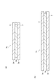
- FIG. 1st Embodiment of this invention It is a perspective view of the polarizing plate of the 1st Embodiment of this invention.
- A) is IIa-IIa sectional drawing of FIG.
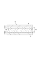
- B) is IIb-IIb sectional drawing of FIG. It is sectional drawing of the polarizing plate of the 2nd Embodiment of this invention. It is sectional drawing of a liquid crystal display device.
- the polarizing plate 1 ⁇ / b> A of the present embodiment is formed by laminating protective films 3 and 3 on both surfaces of a polarizer 2 formed in a thin film shape.
- the protective films 3 and 3 are both formed in the same rectangular shape in plan view, and this shape is also the appearance of the polarizing plate 1A. That is, the polarizing plate 1A has a rectangular shape in plan view.
- the size of the main surface of the polarizing plate 1A that is, the size of the protective films 3 and 3 can be arbitrarily set according to the application target of the polarizing plate 1A.
- the length of the diagonal line is 5 to 250 cm, 10 to 150 cm, 12 to 100 cm.
- the ratio of the lengths of adjacent sides, that is, the aspect ratio of the polarizing plate 1A is preferably 1: 9 to 5: 5, more preferably 2: 8 to 5: 5, and 3: 7. More preferably, it is ⁇ 5: 5.
- the end 2a of the polarizer 2 is located on the inner side of the ends 3a and 3a of the protective films 3 and 3 over the entire circumference. That is, in the cross-sectional view shown in FIG. 2, the side surface of the polarizing plate 1 ⁇ / b> A has a concave shape in which the side surface of the polarizer 2 is recessed with respect to the side surfaces of the protective films 3 and 3.
- the end 2a of the polarizer 2 is preferably positioned 1 to 500 ⁇ m inside the ends 3a and 3a of the protective films 3 and 3, and more preferably positioned 1 to 300 ⁇ m inside. Preferably, it is located 1 to 50 ⁇ m inside.
- the effect of physically protecting the end 2a of the polarizer 2 is particularly high, and a wide display surface is ensured even when an image display device is configured. can do.
- the end 2a of the polarizer 2 is located on the inner side with the same length with respect to the end 3a of the protective film 3 over the entire circumference of the polarizer 2. If the length is not the same over the entire circumference, the polarizing plate 1A has a different lamination state depending on the location, and it is expected that when the curling occurs in the polarizing plate 1A, the curling becomes complicated. Therefore, it is preferable that the side surface of the polarizing plate 1 ⁇ / b> A is recessed with the same length as the side surface of the protective films 3 and 3 on the entire side of the polarizer 2.
- the polarizer 2 may be a stretched film, in which case the end 2a of the polarizer 2 on the side surface perpendicular to the direction of the optical axis (absorption axis) is the end 3a of the protective film 3, 3. It is preferable that it is located inside 3a.
- a side surface parallel to the optical axis has high impact resistance, but a side surface perpendicular to the optical axis or a side surface having an inclination (for example, 40 ° to 140 °) has low impact resistance.
- the end 2a of the polarizer 2 is positioned on the inner side of the ends 3a and 3a of the protective films 3 and 3 on the side surface perpendicular to the optical axis, the end 2a of the polarizer 2 is protected. The effect is particularly achieved.
- the portion of the side surface of the polarizing plate 1A where the side surface of the polarizer 2 is recessed with respect to the side surfaces of the protective films 3 and 3 is preferably not filled with other members. That is, it is preferable that the side surface of the polarizer 2 is open and is in contact with the outside air. If an adhesive or the like, which will be described later, protrudes from the portion, there is a possibility that other portions of the polarizing plate 1A and peripheral equipment to which the polarizing plate 1A is applied are contaminated.
- the protective film 3 by the heat
- the lamination of the polarizer 2 and the protective film 3 may be configured by pasting the polarizer 2 and the protective film 3 formed into a film shape via an adhesive. 1 and 2 do not show the adhesive layer.
- the material of the polarizer 2 a known material that has been conventionally used in the production of polarizing plates can be used.
- the uniaxially stretched film is dyed with iodine or a dichroic dye and then treated with boric acid.
- the film-like polarizer can be cut into an arbitrary size and used at the time of producing the polarizing plate.
- the film-like polarizer 2 produced from these materials has low mechanical strength, thermal stability, and water resistance, and is particularly low at the end of the film. For this reason, the end of the polarizer 2 is likely to be cracked or scratched by handling during the production of the polarizing plate.
- the thickness of the polarizer 2 is preferably 2 to 75 ⁇ m, more preferably 2 to 50 ⁇ m, and still more preferably 2 to 30 ⁇ m.
- the protective film 3 is a film that prevents the main surface and end of the polarizer 2 from being cracked or damaged.
- the “protective film” refers to a film physically laminated at a position closest to the polarizer 2 among various films that can be laminated on the polarizer 2.
- the protective film 3 can be composed of various transparent resin films known in the field of polarizing plates.
- cellulose resin whose typical example is triacetyl cellulose
- polyolefin resin whose typical example is polypropylene resin
- cyclic olefin resin whose typical example is norbornene resin
- acrylic whose typical example is polymethyl methacrylate resin
- polyester resins and polyester resins having polyethylene terephthalate resins as representative examples.
- cellulose resin is representative.
- the protective film 3 may be a film having no optical function, or may be a film having an optical function such as a retardation film or a brightness enhancement film.
- the thickness of the protective film 3 is preferably 5 to 90 ⁇ m, more preferably 5 to 80 ⁇ m, and still more preferably 5 to 50 ⁇ m.
- an adhesive is used in the lamination of the polarizer 2 and the protective film 3
- various adhesives conventionally used for manufacturing polarizing plates can be used as the adhesive.
- an epoxy resin that does not contain an aromatic ring in the molecule is preferable from the viewpoint of weather resistance, refractive index, cationic polymerizability, and the like.
- cures by irradiation of an active energy ray is preferable.
- epoxy resin for example, a hydrogenated epoxy resin, an alicyclic epoxy resin, an aliphatic epoxy resin and the like are preferable.
- polymerization initiators for example, photocationic polymerization initiators for polymerization by ultraviolet irradiation, thermal cationic polymerization initiators for polymerization by heat ray irradiation), and other additives (sensitizers, etc.) Can be added to prepare an epoxy resin composition for coating.
- acrylic resins such as acrylamide, acrylate, urethane acrylate, and epoxy acrylate, and polyvinyl alcohol-based aqueous adhesives can be used.
- the polarizing plate 1A is bonded to one side or both sides of a display cell (image display element) such as a liquid crystal cell.
- the polarizing plate 1 ⁇ / b> A can further include another optical layer laminated on the protective film 3.
- a reflective polarizing film that transmits a certain kind of polarized light and reflects polarized light having the opposite properties; a film with an antiglare function having an uneven surface; a film with a surface antireflection function; surface A reflective film having a reflective function; a transflective film having both a reflective function and a transmissive function; and a viewing angle compensation film.
- the thickness of the polarizing plate 1A comprising three layers of the polarizer 2 and the protective films 3 and 3 is preferably 10 to 500 ⁇ m, more preferably 10 to 300 ⁇ m, and further preferably 10 to 200 ⁇ m. preferable.
- the polarizing plate 1A can be manufactured as follows, for example. First, two protective films 3 and 3 are cut out into a rectangle from a long film roll made of a material constituting the protective film 3. The size and aspect ratio of the rectangle to be cut out are determined according to the application target of the polarizing plate 1A. An adhesive is applied to one side of one protective film (first protective film) 3. The region where the adhesive is applied is not the entire surface of the protective film 3, but the region where the film-like polarizer 2 is laminated.
- the polarizer 2 is cut into a rectangle from a long film roll made of the material constituting the polarizer 2.
- the size of the rectangle to be cut out is smaller than the size of the protective film 3.
- the cut-out film-like polarizer 2 is laminated on the surface of the protective film 3 coated with an adhesive.
- the lamination here is performed so that the entire surface of one side of the polarizer 2 enters the inside of the surface of the protective film 3.
- the polarizer 2 is covered with the protective film.
- an active energy ray-curable resin is used as the adhesive, the adhesive is cured by irradiating active energy rays here.
- an adhesive is applied to the entire surface of the other side of the polarizer, and the remaining protective film (second protective film) 3 is laminated.
- stacking of the protective film 3 here is performed so that the whole surface of the single side
- the active energy ray-curable resin is used as the adhesive, the active energy ray is irradiated here to cure the adhesive.
- the polarizing plate 1A is manufactured by the above procedure.
- the end 2a of the polarizer 2 is located inside the end 3a of the protective film 3, the end of the polarizer 2 is physically protected. Accordingly, in handling such as when the polarizing plate 1A is attached to a liquid crystal cell, for example, when the side surface of the polarizing plate 1A receives an impact, only the end portion 3a of the protective film 3 receives the impact, and the polarizer 2 Scratches and cracks are prevented from occurring at the ends of the. This effect is also exhibited in further handling after the polarizing plate 1A is attached to a liquid crystal cell or the like. Moreover, it contributes to the durability improvement of the heat shock test of the polarizing plate 1A.
- the polarizing plate 1 ⁇ / b> A has an end portion 2 a of the polarizer 2 protected by the end portions 3 a and 3 a of the protective films 3 and 3 laminated on both surfaces of the polarizer 2.
- the effect is favorably exhibited in the tendency to change. That is, when the frame of the liquid crystal cell to which the polarizing plate 1A is attached has a normal width, the liquid crystal cell itself has a function of protecting the polarizer 2 from physical shock, but the liquid crystal cell has a narrow frame. If it exists, the effect of the protection becomes small. In this case, the ratio that the end 3a of the protective film 3 on the liquid crystal cell side contributes to the protection of the end 2a of the polarizer 2 is increased.
- the TV screen or mobile terminal When applied to a screen, it is easy to secure a wide display surface.
- the polarizing plate 1A has a rectangular shape in plan view, it can be easily applied to various articles such as a liquid crystal display device.
- a separator 4 and a temporary protective film 6 may be further laminated on a laminate of the polarizer 2 and the protective film 3.
- the polarizing plate 1 ⁇ / b> B of the second embodiment is disposed on one side of the polarizing plate 1 ⁇ / b> A of the first embodiment (that is, on the surface of the one protective film 3 on which the polarizer 2 is not laminated) via the pressure-sensitive adhesive layer 5.
- the separator 4 is laminated.
- a temporary protective film 6 is laminated on the other surface of the polarizing plate 1A (that is, on the surface of the other protective film 3 on which the polarizer 2 is not laminated).
- the pressure-sensitive adhesive layer 5 is a layer that functions when the polarizing plate 1B is attached to another article (for example, a liquid crystal cell).
- the pressure-sensitive adhesive layer 5 can be composed of acrylic resin, silicone resin, polyester, polyurethane, polyether, or the like.
- the thickness of the pressure-sensitive adhesive layer 5 is preferably 2 to 500 ⁇ m, more preferably 2 to 200 ⁇ m, still more preferably 2 to 50 ⁇ m.
- a method of laminating the pressure-sensitive adhesive layer 5 on the protective film 3 for example, a method of applying a solution containing the resin or any additive component to the protective film 3 may be used. After forming, the method of laminating
- the end 5a of the pressure-sensitive adhesive layer 5 is preferably aligned with the end 3a of the protective film 3 over the entire circumference.
- the separator 4 is a peelable film that is stuck for the purpose of protecting the pressure-sensitive adhesive layer 5 and preventing adhesion of foreign matters, and is peeled off when the polarizing plate 1B is used to expose the pressure-sensitive adhesive layer 5.
- the separator 4 can be made of, for example, a polyethylene resin such as polyethylene, a polypropylene resin such as polypropylene, a polyester resin such as polyethylene terephthalate, or the like. Among these, a stretched film of polyethylene terephthalate is preferable.
- the end 4a of the separator 4 is preferably aligned with the end 5a of the adhesive layer 5 over the entire circumference. Further, the separator 4 may be subjected to a release treatment with a silicone resin or the like on the surface in contact with the pressure-sensitive adhesive layer 5 so that the separator 4 can be easily peeled off when the polarizing plate 1B is used.
- the thickness of the separator 4 is preferably 5 to 200 ⁇ m, more preferably 5 to 150 ⁇ m, still more preferably 5 to 100 ⁇ m.
- the temporary protective film 6 is a peelable film and is a film for protecting the surface of the protective film 3 on which the temporary protective film 6 is laminated from being damaged or worn.
- the same material as that of the protective film 3 can be used, and polyester resins such as polyethylene terephthalate, polyethylene naphthalate, polyethylene isophthalate, and polybutylene terephthalate are particularly preferable.
- the temporary protective film 6 may have a pressure-sensitive adhesive layer having weak adhesion laminated on the surface of the film in addition to the film serving as the base material.
- the temporary protective film 6 is laminated on the protective film 3 and then bonded to the protective film 3 until the polarizing plate 1B is used.
- the temporary protective film 6 is peeled off from the protective film 3 when used.
- the end 6a of the temporary protective film 6 is preferably aligned with the end 3a of the protective film 3 over the entire circumference.
- the thickness of the temporary protective film 6 is preferably 5 to 200 ⁇ m, more preferably 5 to 150 ⁇ m, and still more preferably 5 to 100 ⁇ m.
- the protective film 3 is prevented from being damaged or worn, and when the polarizing plate 1B is used, the separator 4 is peeled off to expose the adhesive layer 5, and the polarizing plate 1B is removed by the adhesive force.
- An image display device can be configured by sticking to an article such as a liquid crystal cell or an organic EL device.
- a liquid crystal cell as an example, as shown in FIG. 4, for example, a polarizing plate 1 ⁇ / b> B with a separator 4 peeled off is adhered to both surfaces of a liquid crystal cell 8 to form a liquid crystal panel 9.
- the liquid crystal display device 10 can be manufactured by combining other members.
- a touch panel or the like can be provided on the surface exposed by peeling off the temporary protective film 6.
- the present invention is not limited to the above embodiment.
- the end part 2a of the polarizer 2 showed the aspect located inside the edge part 3a, 3a of both the protective films 3 and 3 over the perimeter in the said embodiment, it is located inside.
- the part to perform does not need to cover the whole periphery of the polarizer 2.
- the end 2a of the polarizer 2 is protected only at the portion located on the inner side of the ends 3a and 3a of the protective films 3 and 3.
- the end 2a of the polarizer 2 (two opposite sides of the polarizer 2) on the side surface perpendicular to the direction of the optical axis of the polarizer 2 is inside the ends 3a and 3a of the protective films 3 and 3. May be located.
- the entire length of the polarizer 2 is shown to be located on the inner side with the same length.
- the degree of the depression of the polarizer 2 may be changed depending on the location. For example, if a part that is susceptible to impact during handling of the polarizing plate is known in advance, the above-described complicated curl may occur, but the width of the dent at the end of the polarizer may be increased. preferable.
- the one protective film 3 may have the same shape as the polarizer 2. That is, the end 3 a of one protective film 3 may be aligned with the end 2 a of the polarizer 2.
- the polarizing plate 1A, 1B showed the example which is planar view rectangle in the said embodiment, other squares, for example, a trapezoid, a parallelogram, a square, etc. may be sufficient, and it may be circular or elliptical. Also good. That is, the polarizing plates 1A and 1B can have any shape according to the shape of the article to which the polarizing plates 1A and 1B are attached. In particular, the shape in plan view is the region where the polarizing plates 1A and 1B are attached. The shape may match the shape.
- SYMBOLS 1A, 1B ... Polarizing plate, 2 ... Polarizer, 2a ... End of polarizer, 3 ... Protective film, 3a ... End of protective film, 4 ... Separator, 4a ... End of separator, 5 ... Adhesive layer, 5a ... end of pressure-sensitive adhesive layer, 6 ... temporary protective film, 6a ... end of temporary protective film, 8 ... liquid crystal cell, 9 ... liquid crystal panel, 10 ... liquid crystal display device (image display device).
Landscapes
- Physics & Mathematics (AREA)
- Nonlinear Science (AREA)
- General Physics & Mathematics (AREA)
- Optics & Photonics (AREA)
- Mathematical Physics (AREA)
- Chemical & Material Sciences (AREA)
- Crystallography & Structural Chemistry (AREA)
- Polarising Elements (AREA)
- Liquid Crystal (AREA)
Abstract
Description
図1及び図2に示されているとおり、本実施形態の偏光板1Aは、薄膜状に形成された偏光子2の両面の全面に保護フィルム3,3が積層されて成っている。保護フィルム3,3はいずれも平面視長方形の同形に成形されており、この形状が偏光板1Aの外観形状ともなっている。すなわち、偏光板1Aは、平面視長方形をなしている。
本発明の偏光板は、図3に示されているとおり、偏光子2及び保護フィルム3の積層体に対して、セパレータ4や仮保護フィルム6が更に積層されていてもよい。
Claims (8)
- 偏光子と、その両面に積層された保護フィルムと、を備え、
前記保護フィルムは、いずれも所定の形状に成形されたものであり、
前記保護フィルムは、それぞれ前記偏光子の片面の全面に積層されており、
前記偏光子の少なくとも一部の端部が、少なくとも一方の前記保護フィルムの端部よりも内側に位置している、偏光板。 - 前記偏光子の少なくとも一部の端部が、両方の前記保護フィルムの端部よりも内側に位置している、請求項1記載の偏光板。
- 前記偏光子の全ての端部が、少なくとも一方の前記保護フィルムの端部よりも内側に位置している、請求項1又は2記載の偏光板。
- 平面視形状が、当該偏光板を貼着する領域の形状に一致する形状である、請求項1~3のいずれか一項記載の偏光板。
- 平面視四角形である、請求項1~4のいずれか一項記載の偏光板。
- いずれかの前記保護フィルムの前記偏光子が積層されていない側に、粘着剤層を介してセパレータが積層されており、
他方の前記保護フィルムの前記偏光子が積層されていない側に、仮保護フィルムが積層されている、請求項1~5のいずれか一項記載の偏光板。 - 請求項1~5のいずれか一項記載の偏光板を備える画像表示装置。
- 所定の形状に成形された第1の保護フィルムに、片面の全面が前記第1の保護フィルムに覆われるように偏光子を積層し、
前記偏光子に、前記偏光子の他方の片面の全面を覆うように第2の保護フィルムを積層する、偏光板の製造方法であって、
前記偏光子が前記第1の保護フィルム及び前記第2の保護フィルムの少なくとも一方の保護フィルムの少なくとも一部の端部よりも内側に位置するように、前記第1の保護フィルム、前記偏光子、及び前記第2の保護フィルムを積層する、偏光板の製造方法。
Priority Applications (3)
| Application Number | Priority Date | Filing Date | Title |
|---|---|---|---|
| JP2016553482A JP6279093B2 (ja) | 2015-08-10 | 2016-08-05 | 偏光板、画像表示装置、及び偏光板の製造方法 |
| KR1020187003117A KR101945164B1 (ko) | 2015-08-10 | 2016-08-05 | 편광판, 화상 표시 장치 및 편광판의 제조 방법 |
| CN201680045811.0A CN107850724B (zh) | 2015-08-10 | 2016-08-05 | 偏振板、图像显示装置及偏振板的制造方法 |
Applications Claiming Priority (4)
| Application Number | Priority Date | Filing Date | Title |
|---|---|---|---|
| JP2015-157955 | 2015-08-10 | ||
| JP2015157955 | 2015-08-10 | ||
| JPPCT/JP2015/083266 | 2015-11-26 | ||
| PCT/JP2015/083266 WO2017026078A1 (ja) | 2015-08-10 | 2015-11-26 | 偏光板、画像表示装置、及び偏光板の製造方法 |
Publications (1)
| Publication Number | Publication Date |
|---|---|
| WO2017026403A1 true WO2017026403A1 (ja) | 2017-02-16 |
Family
ID=57983650
Family Applications (2)
| Application Number | Title | Priority Date | Filing Date |
|---|---|---|---|
| PCT/JP2015/083266 Ceased WO2017026078A1 (ja) | 2015-08-10 | 2015-11-26 | 偏光板、画像表示装置、及び偏光板の製造方法 |
| PCT/JP2016/073152 Ceased WO2017026403A1 (ja) | 2015-08-10 | 2016-08-05 | 偏光板、画像表示装置、及び偏光板の製造方法 |
Family Applications Before (1)
| Application Number | Title | Priority Date | Filing Date |
|---|---|---|---|
| PCT/JP2015/083266 Ceased WO2017026078A1 (ja) | 2015-08-10 | 2015-11-26 | 偏光板、画像表示装置、及び偏光板の製造方法 |
Country Status (5)
| Country | Link |
|---|---|
| JP (2) | JP6279093B2 (ja) |
| KR (1) | KR101945164B1 (ja) |
| CN (1) | CN107850724B (ja) |
| TW (1) | TWI644130B (ja) |
| WO (2) | WO2017026078A1 (ja) |
Families Citing this family (5)
| Publication number | Priority date | Publication date | Assignee | Title |
|---|---|---|---|---|
| TWI672533B (zh) * | 2017-11-16 | 2019-09-21 | 住華科技股份有限公司 | 偏光板 |
| TWI694924B (zh) * | 2018-11-20 | 2020-06-01 | 住華科技股份有限公司 | 偏光板及包含其之顯示裝置、偏光板的製造方法、以及顯示裝置的製造方法 |
| KR102471941B1 (ko) * | 2021-06-04 | 2022-11-29 | 동우 화인켐 주식회사 | 광학 적층체 및 이의 제조방법과, 이를 포함하는 스마트 윈도우 및 이를 적용한 자동차 또는 건물용 창호 |
| KR102848206B1 (ko) * | 2021-06-04 | 2025-08-21 | 동우 화인켐 주식회사 | 광학 적층체 및 이의 제조방법과, 이를 포함하는 스마트 윈도우 및 이를 적용한 자동차 또는 건물용 창호 |
| KR20220164288A (ko) * | 2021-06-04 | 2022-12-13 | 동우 화인켐 주식회사 | 광학 적층체 및 이의 제조방법과, 이를 포함하는 스마트 윈도우 및 이를 적용한 자동차 또는 건물용 창호 |
Citations (6)
| Publication number | Priority date | Publication date | Assignee | Title |
|---|---|---|---|---|
| JPS62158423U (ja) * | 1986-03-29 | 1987-10-08 | ||
| JPH10206633A (ja) * | 1997-01-22 | 1998-08-07 | Casio Comput Co Ltd | 偏光板およびその製造方法 |
| JP2006088651A (ja) * | 2004-09-27 | 2006-04-06 | Nitto Denko Corp | フィルム積層物の製造方法、及びそれに用いる製造装置 |
| WO2006077920A1 (ja) * | 2005-01-20 | 2006-07-27 | Nitto Denko Corporation | 偏光板の製造方法、偏光板、光学フィルムおよびそれらを用いた画像表示装置 |
| WO2012165184A1 (ja) * | 2011-05-31 | 2012-12-06 | 住友化学株式会社 | 複合偏光板および液晶表示装置 |
| JP2013186252A (ja) * | 2012-03-07 | 2013-09-19 | Nitto Denko Corp | 偏光板の製造方法 |
Family Cites Families (10)
| Publication number | Priority date | Publication date | Assignee | Title |
|---|---|---|---|---|
| JPH11254550A (ja) * | 1998-03-12 | 1999-09-21 | Nitto Denko Corp | 光学部材 |
| JP4974261B2 (ja) | 2001-04-09 | 2012-07-11 | 日東電工株式会社 | 光学部材 |
| JP4208187B2 (ja) * | 2002-10-28 | 2009-01-14 | 日東電工株式会社 | 粘着型光学フィルム、粘着型光学フィルムの製造方法および画像表示装置 |
| JP5058953B2 (ja) * | 2007-12-06 | 2012-10-24 | 日東電工株式会社 | 光学表示ユニットの製造方法およびそれに用いられるロール原反 |
| JP4785944B2 (ja) * | 2008-04-16 | 2011-10-05 | 日東電工株式会社 | 光学表示装置の製造方法 |
| JP2010277018A (ja) | 2009-06-01 | 2010-12-09 | Sumitomo Chemical Co Ltd | 耐久性に優れた偏光板およびその製造方法、それを用いた画像表示装置 |
| JP5750848B2 (ja) * | 2010-08-26 | 2015-07-22 | 住友化学株式会社 | 画像表示装置用光学部材 |
| JP2012194475A (ja) * | 2011-03-17 | 2012-10-11 | Sumitomo Chemical Co Ltd | 偏光板、偏光板の製造方法および液晶表示装置 |
| KR101839651B1 (ko) * | 2012-02-03 | 2018-04-26 | 스미또모 가가꾸 가부시키가이샤 | 편광성 적층 필름 및 그 제조방법 |
| JP6154099B2 (ja) | 2012-02-03 | 2017-06-28 | 住友化学株式会社 | 偏光性積層フィルムの製造方法及び偏光板の製造方法 |
-
2015
- 2015-11-26 WO PCT/JP2015/083266 patent/WO2017026078A1/ja not_active Ceased
-
2016
- 2016-08-05 WO PCT/JP2016/073152 patent/WO2017026403A1/ja not_active Ceased
- 2016-08-05 KR KR1020187003117A patent/KR101945164B1/ko active Active
- 2016-08-05 JP JP2016553482A patent/JP6279093B2/ja active Active
- 2016-08-05 CN CN201680045811.0A patent/CN107850724B/zh active Active
- 2016-08-10 TW TW105125421A patent/TWI644130B/zh active
-
2017
- 2017-09-26 JP JP2017184956A patent/JP2018028668A/ja active Pending
Patent Citations (6)
| Publication number | Priority date | Publication date | Assignee | Title |
|---|---|---|---|---|
| JPS62158423U (ja) * | 1986-03-29 | 1987-10-08 | ||
| JPH10206633A (ja) * | 1997-01-22 | 1998-08-07 | Casio Comput Co Ltd | 偏光板およびその製造方法 |
| JP2006088651A (ja) * | 2004-09-27 | 2006-04-06 | Nitto Denko Corp | フィルム積層物の製造方法、及びそれに用いる製造装置 |
| WO2006077920A1 (ja) * | 2005-01-20 | 2006-07-27 | Nitto Denko Corporation | 偏光板の製造方法、偏光板、光学フィルムおよびそれらを用いた画像表示装置 |
| WO2012165184A1 (ja) * | 2011-05-31 | 2012-12-06 | 住友化学株式会社 | 複合偏光板および液晶表示装置 |
| JP2013186252A (ja) * | 2012-03-07 | 2013-09-19 | Nitto Denko Corp | 偏光板の製造方法 |
Also Published As
| Publication number | Publication date |
|---|---|
| WO2017026078A1 (ja) | 2017-02-16 |
| TW201727281A (zh) | 2017-08-01 |
| JPWO2017026403A1 (ja) | 2017-08-10 |
| JP2018028668A (ja) | 2018-02-22 |
| TWI644130B (zh) | 2018-12-11 |
| CN107850724A (zh) | 2018-03-27 |
| KR101945164B1 (ko) | 2019-02-01 |
| CN107850724B (zh) | 2019-04-23 |
| JP6279093B2 (ja) | 2018-02-14 |
| KR20180030564A (ko) | 2018-03-23 |
Similar Documents
| Publication | Publication Date | Title |
|---|---|---|
| KR101727871B1 (ko) | 편광판의 셋트 및 전면판 일체형 액정 표시 패널 | |
| CN106415339B (zh) | 光学层叠体及图像显示装置 | |
| JP6749294B2 (ja) | 積層光学フィルムの製造方法 | |
| JP6279093B2 (ja) | 偏光板、画像表示装置、及び偏光板の製造方法 | |
| JP5997355B1 (ja) | 粘着剤層付き偏光板、及び画像表示装置 | |
| KR102535072B1 (ko) | 편광판 및 액정 표시 장치 | |
| JP6188868B1 (ja) | 偏光板、及び液晶表示装置 | |
| JP5871407B1 (ja) | 偏光板 | |
| KR101757062B1 (ko) | 편광판 및 액정 표시 장치 | |
| KR20190015323A (ko) | 적층 필름, 마크가 형성된 적층 필름의 제조 방법 및 화상 표시 장치의 제조 방법 | |
| KR20170101809A (ko) | 편광판 세트 및 액정 패널 | |
| WO2020262143A1 (ja) | 光学積層体 | |
| TWI704058B (zh) | 積層光學膜之製造方法 | |
| KR20170113168A (ko) | 광학 필름 및 편광판 | |
| JP6782676B2 (ja) | 偏光板、及び液晶表示装置 | |
| JP2017211663A (ja) | 偏光板、及び液晶表示装置 | |
| JP2022044597A (ja) | 光学フィルム原反ロールの製造方法、および光学部材シートの製造方法 | |
| WO2017134753A1 (ja) | 偏光板 |
Legal Events
| Date | Code | Title | Description |
|---|---|---|---|
| ENP | Entry into the national phase |
Ref document number: 2016553482 Country of ref document: JP Kind code of ref document: A |
|
| 121 | Ep: the epo has been informed by wipo that ep was designated in this application |
Ref document number: 16835100 Country of ref document: EP Kind code of ref document: A1 |
|
| ENP | Entry into the national phase |
Ref document number: 20187003117 Country of ref document: KR Kind code of ref document: A |
|
| NENP | Non-entry into the national phase |
Ref country code: DE |
|
| 122 | Ep: pct application non-entry in european phase |
Ref document number: 16835100 Country of ref document: EP Kind code of ref document: A1 |