WO2017013838A1 - 吸熱素子及びそれを備えた半導体装置並びに吸熱素子の製造方法 - Google Patents
吸熱素子及びそれを備えた半導体装置並びに吸熱素子の製造方法 Download PDFInfo
- Publication number
- WO2017013838A1 WO2017013838A1 PCT/JP2016/003103 JP2016003103W WO2017013838A1 WO 2017013838 A1 WO2017013838 A1 WO 2017013838A1 JP 2016003103 W JP2016003103 W JP 2016003103W WO 2017013838 A1 WO2017013838 A1 WO 2017013838A1
- Authority
- WO
- WIPO (PCT)
- Prior art keywords
- film
- semiconductor
- heat
- layer
- metal
- Prior art date
- Legal status (The legal status is an assumption and is not a legal conclusion. Google has not performed a legal analysis and makes no representation as to the accuracy of the status listed.)
- Ceased
Links
Images








Classifications
-
- H—ELECTRICITY
- H10—SEMICONDUCTOR DEVICES; ELECTRIC SOLID-STATE DEVICES NOT OTHERWISE PROVIDED FOR
- H10N—ELECTRIC SOLID-STATE DEVICES NOT OTHERWISE PROVIDED FOR
- H10N10/00—Thermoelectric devices comprising a junction of dissimilar materials, i.e. devices exhibiting Seebeck or Peltier effects
- H10N10/01—Manufacture or treatment
-
- H—ELECTRICITY
- H10—SEMICONDUCTOR DEVICES; ELECTRIC SOLID-STATE DEVICES NOT OTHERWISE PROVIDED FOR
- H10N—ELECTRIC SOLID-STATE DEVICES NOT OTHERWISE PROVIDED FOR
- H10N10/00—Thermoelectric devices comprising a junction of dissimilar materials, i.e. devices exhibiting Seebeck or Peltier effects
- H10N10/10—Thermoelectric devices comprising a junction of dissimilar materials, i.e. devices exhibiting Seebeck or Peltier effects operating with only the Peltier or Seebeck effects
- H10N10/13—Thermoelectric devices comprising a junction of dissimilar materials, i.e. devices exhibiting Seebeck or Peltier effects operating with only the Peltier or Seebeck effects characterised by the heat-exchanging means at the junction
-
- H—ELECTRICITY
- H10—SEMICONDUCTOR DEVICES; ELECTRIC SOLID-STATE DEVICES NOT OTHERWISE PROVIDED FOR
- H10N—ELECTRIC SOLID-STATE DEVICES NOT OTHERWISE PROVIDED FOR
- H10N10/00—Thermoelectric devices comprising a junction of dissimilar materials, i.e. devices exhibiting Seebeck or Peltier effects
- H10N10/10—Thermoelectric devices comprising a junction of dissimilar materials, i.e. devices exhibiting Seebeck or Peltier effects operating with only the Peltier or Seebeck effects
- H10N10/17—Thermoelectric devices comprising a junction of dissimilar materials, i.e. devices exhibiting Seebeck or Peltier effects operating with only the Peltier or Seebeck effects characterised by the structure or configuration of the cell or thermocouple forming the device
-
- H—ELECTRICITY
- H10—SEMICONDUCTOR DEVICES; ELECTRIC SOLID-STATE DEVICES NOT OTHERWISE PROVIDED FOR
- H10N—ELECTRIC SOLID-STATE DEVICES NOT OTHERWISE PROVIDED FOR
- H10N10/00—Thermoelectric devices comprising a junction of dissimilar materials, i.e. devices exhibiting Seebeck or Peltier effects
- H10N10/80—Constructional details
- H10N10/85—Thermoelectric active materials
- H10N10/851—Thermoelectric active materials comprising inorganic compositions
-
- H—ELECTRICITY
- H10—SEMICONDUCTOR DEVICES; ELECTRIC SOLID-STATE DEVICES NOT OTHERWISE PROVIDED FOR
- H10N—ELECTRIC SOLID-STATE DEVICES NOT OTHERWISE PROVIDED FOR
- H10N10/00—Thermoelectric devices comprising a junction of dissimilar materials, i.e. devices exhibiting Seebeck or Peltier effects
- H10N10/80—Constructional details
- H10N10/85—Thermoelectric active materials
- H10N10/851—Thermoelectric active materials comprising inorganic compositions
- H10N10/855—Thermoelectric active materials comprising inorganic compositions comprising compounds containing boron, carbon, oxygen or nitrogen
-
- H—ELECTRICITY
- H10—SEMICONDUCTOR DEVICES; ELECTRIC SOLID-STATE DEVICES NOT OTHERWISE PROVIDED FOR
- H10N—ELECTRIC SOLID-STATE DEVICES NOT OTHERWISE PROVIDED FOR
- H10N10/00—Thermoelectric devices comprising a junction of dissimilar materials, i.e. devices exhibiting Seebeck or Peltier effects
- H10N10/80—Constructional details
- H10N10/85—Thermoelectric active materials
- H10N10/851—Thermoelectric active materials comprising inorganic compositions
- H10N10/8556—Thermoelectric active materials comprising inorganic compositions comprising compounds containing germanium or silicon
-
- H—ELECTRICITY
- H10—SEMICONDUCTOR DEVICES; ELECTRIC SOLID-STATE DEVICES NOT OTHERWISE PROVIDED FOR
- H10N—ELECTRIC SOLID-STATE DEVICES NOT OTHERWISE PROVIDED FOR
- H10N19/00—Integrated devices, or assemblies of multiple devices, comprising at least one thermoelectric or thermomagnetic element covered by groups H10N10/00 - H10N15/00
-
- H—ELECTRICITY
- H10—SEMICONDUCTOR DEVICES; ELECTRIC SOLID-STATE DEVICES NOT OTHERWISE PROVIDED FOR
- H10N—ELECTRIC SOLID-STATE DEVICES NOT OTHERWISE PROVIDED FOR
- H10N10/00—Thermoelectric devices comprising a junction of dissimilar materials, i.e. devices exhibiting Seebeck or Peltier effects
- H10N10/80—Constructional details
- H10N10/85—Thermoelectric active materials
- H10N10/851—Thermoelectric active materials comprising inorganic compositions
- H10N10/852—Thermoelectric active materials comprising inorganic compositions comprising tellurium, selenium or sulfur
Definitions
- the present invention relates to a heat absorbing element, a semiconductor device including the same, and a method for manufacturing the heat absorbing element.
- a power semiconductor device including a cooling element such as a Peltier element is known in order to improve heat dissipation from the power semiconductor device to the outside.
- the present invention has been made in view of such a point, and the object of the present invention is to reduce the thermal resistance between the semiconductor element and the endothermic element in the thin-film endothermic element formed on the semiconductor element. It is to be able to reduce and to establish the manufacturing method.
- the present invention is characterized in that a Peltier-type heat absorption element formed in a semiconductor element is formed in a thin film shape.
- the present invention is directed to a heat absorbing element, a semiconductor device including the same, and a method of manufacturing the heat absorbing element, and has taken the following solutions.
- the first invention is directed to a Peltier-type thin-film endothermic element that is thermally connected to the surface of a semiconductor element through an electrical insulator, and heat in bulk in a material constituting the endothermic element.
- the conductivity is 50 W / mK or more, and the Seebeck coefficient is 300 ⁇ V / K or more.
- the thermal resistance between the semiconductor element and the heat absorbing element can be reduced, and the heat dissipation of the semiconductor element can be improved.
- the substance includes silicon (Si), silicon carbide (SiC), gallium nitride (GaN), aluminum nitride (AlN), boron nitride (BN), and diamond (C ).
- the substance is silicon.
- the substance constitutes a p-type or n-type semiconductor layer
- the p-type semiconductor layer and the n-type semiconductor layer include a semiconductor element and an electrical insulator. Are arranged in parallel.
- a Peltier element as a thin-film heat absorption element can be reliably formed, and the contact area between the semiconductor element and the electrical insulator can be increased, and the efficiency of the heat absorption effect (heat radiation effect) is improved.
- the fifth invention is the above first to fourth invention, wherein the semiconductor device is directly formed and thermally connected to the heat exhaust side.
- the heat absorption efficiency of the heat absorption element is improved, and the heat dissipation effect of the semiconductor element is improved.
- the sixth invention covers the region of 10% or more of the area of the heat generation source in the semiconductor element in the first to fifth inventions.
- the heat dissipation effect of the semiconductor element can be improved.
- a seventh aspect of the invention is a semiconductor device including the heat absorbing element according to the first to sixth aspects of the invention.
- the semiconductor device of the present invention includes the heat absorbing element of the present invention, the heat dissipation of the semiconductor element can be improved.
- the semiconductor element is a power semiconductor element.
- the heat dissipation of the power semiconductor element that becomes high temperature during operation can be improved.
- the semiconductor element is a SiC-based power semiconductor element made of silicon carbide.
- a tenth aspect of the present invention is directed to a method of manufacturing a Peltier-type thin-film endothermic element that is thermally connected to a surface of a semiconductor element through an electrical insulator.
- a step of sequentially forming a lower metal film, a first conductive type semiconductor layer, and a first metal sacrificial film via an electrical insulator, and a first patterning of the first conductive type semiconductor layer from the first metal sacrificial film Forming a plurality of first conductivity type semiconductor blocks from the first conductivity type semiconductor layer by forming a metal mask film and patterning the first conductivity type semiconductor layer using the formed first metal mask film; , Sequentially forming a second conductive type semiconductor layer and a second metal sacrificial layer on the lower metal layer including the first conductive type semiconductor block, and patterning the second conductive type semiconductor layer from the second metal sacrificial layer.
- Second metal mask film Forming a plurality of second conductivity type semiconductor blocks from the second conductivity type semiconductor layer by patterning the second conductivity type semiconductor layer using the formed and formed second metal mask film; and a lithography method
- the semiconductor element is exposed by selectively etching the electrode formation region of the semiconductor element in the lower metal film, and the first conductive semiconductor block and the second conductive semiconductor in the lower metal film are formed by lithography.
- the endothermic element is formed on the semiconductor element via the electrical insulator, the lower metal film serving as the lower electrode of the endothermic element, the first conductive type semiconductor layer, the second conductive type semiconductor layer, and It can be formed by etching the lower metal electrode of the heat absorbing element and the upper metal film to be the electrode of the semiconductor element.
- the first conductive semiconductor layer and the second conductive semiconductor layer are formed of silicon (Si), silicon carbide (SiC), gallium nitride (GaN), aluminum nitride (AlN), One of boron nitride (BN) and diamond (C).
- the lower metal film, the first metal sacrificial film, the second metal sacrificial film, and the upper metal film are made of nickel, and the lower metal film, the first metal sacrificial film, For the patterning of at least one of the two-metal sacrificial film and the upper metal film, wet etching using a mixture of concentrated hydrochloric acid, concentrated hydrogen peroxide solution and pure water (hydrochloric acid excess water) as an etchant is used.
- the nickel film can be etched without deteriorating the resist.
- the first metal sacrificial film and the second metal sacrificial film are made of nickel, the first conductive semiconductor layer and the second conductive semiconductor layer are made of silicon,
- the step of forming the first conductivity type semiconductor block and the second conductivity type semiconductor block is dry etching using chlorine and hydrogen bromide.
- the first metal when performing the etching for forming the first conductive semiconductor block and the second conductive semiconductor block from the first conductive semiconductor layer made of silicon and the second conductive semiconductor layer, the first metal made of nickel.
- the first metal sacrificial film serving as the mask film and the second metal sacrificial film serving as the second metal mask film can be used as the hard mask.
- the semiconductor element is a power semiconductor element.
- the heat dissipation of the power semiconductor element that becomes high temperature during operation can be improved.
- the semiconductor element is an SiC power semiconductor element made of silicon carbide.
- the thermal resistance between the semiconductor element and the endothermic element can be greatly reduced, and a thin-film endothermic element formed on the surface of the semiconductor element can be reliably formed.
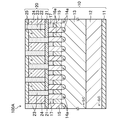
- FIG. 1 is a cross-sectional view showing the main part of the semiconductor device according to the first embodiment of the present invention.
- FIG. 2 is a cross-sectional view showing a main part of a semiconductor device according to a first modification of the first embodiment of the present invention.
- FIG. 3 is a cross-sectional view showing a main part of a semiconductor device according to a second modification of the first embodiment of the present invention.
- FIG. 4 is a cross-sectional view showing a main part of a semiconductor device according to the second embodiment of the present invention.
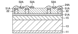
- FIG. 5 is a cross-sectional view showing a main part of a method for manufacturing a semiconductor device according to the third embodiment of the present invention.
- FIG. 1 is a cross-sectional view showing the main part of the semiconductor device according to the first embodiment of the present invention.
- FIG. 2 is a cross-sectional view showing a main part of a semiconductor device according to a first modification of the first embodiment of the present invention.
- FIG. 3 is a cross
- FIG. 6 is a cross-sectional view showing a main part of a method for manufacturing a semiconductor device according to the third embodiment of the present invention.
- FIG. 7 is a cross-sectional view showing a main part of a method for manufacturing a semiconductor device according to the third embodiment of the present invention.
- FIG. 8 is a cross-sectional view showing a main part of a method for manufacturing a semiconductor device according to the third embodiment of the present invention.
- FIG. 9 is a cross-sectional view showing a main part of a method for manufacturing a semiconductor device according to the third embodiment of the present invention.
- FIG. 10 is a cross-sectional view showing a main part of a method for manufacturing a semiconductor device according to the third embodiment of the present invention.
- FIG. 10 is a cross-sectional view showing a main part of a method for manufacturing a semiconductor device according to the third embodiment of the present invention.
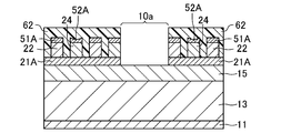
- FIG. 11 is a cross-sectional view showing a main part of a method for manufacturing a semiconductor device according to the third embodiment of the present invention.
- FIG. 12 is a cross-sectional view showing a main part of a method for manufacturing a semiconductor device according to the third embodiment of the present invention.
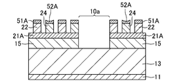
- FIG. 13 is a cross-sectional view showing a main part of a method for manufacturing a semiconductor device according to the third embodiment of the present invention.
- FIG. 14 is a cross-sectional view showing a main part of a method for manufacturing a semiconductor device according to the third embodiment of the present invention.
- FIG. 15 is a cross-sectional view showing a main part of a method for manufacturing a semiconductor device according to the third embodiment of the present invention.
- FIG. 12 is a cross-sectional view showing a main part of a method for manufacturing a semiconductor device according to the third embodiment of the present invention.
- FIG. 13 is a cross-sectional view showing a main part of a method for manufacturing a semiconductor device
- FIG. 16 is a cross-sectional view showing a main part of a method for manufacturing a semiconductor device according to the third embodiment of the present invention.
- FIG. 17 is a cross-sectional view showing a main part of a method for manufacturing a semiconductor device according to the third embodiment of the present invention.
- FIG. 18 is a cross-sectional view showing a main part of a method for manufacturing a semiconductor device according to the third embodiment of the present invention.
- FIG. 19 is a schematic view showing an example of a heat absorbing element according to an embodiment of the present invention.
- FIG. 20 shows the drive current dependence of the total heat transfer amount when the lower limit values of the Seebeck coefficient and the thermal conductivity are set for the Peltier device according to one embodiment and the total heat transfer amount of the Peltier device using the conventional bismuth tellurium. It is the graph which compared sex.
- FIG. 21 is a graph showing the drive current dependence of the total heat transfer amount for each material that can be used in the Peltier device according to one embodiment.
- FIG. 1 shows a cross-sectional configuration of a main part of a semiconductor device according to the first embodiment of the present invention.
- the semiconductor device 100 includes a semiconductor element body 10 and a heat absorption element 20 integrally formed on the semiconductor element body 10.
- the semiconductor element body 10 is a Schottky barrier diode (hereinafter also abbreviated as SBD).
- SiC silicon carbide
- the semiconductor element body 10 includes, for example, a bulk layer (contact layer) 12 made of n + -type SiC, and a drift layer 13 made of n-type SiC epitaxially grown on the bulk layer 12 to regulate the breakdown voltage.
- FIG. 1 for convenience, one of the plurality of cathode electrodes 16 is illustrated, but a plurality of cathode electrodes 16 having the same shape are arranged in a lateral direction (two-dimensionally) at a predetermined interval. ing.
- NiSi x nickel silicide
- Ni nickel
- Ni nickel
- a p + region 14 for improving the breakdown voltage of the SBD is formed in the peripheral portion facing the cathode electrode 16 in the upper part of the drift layer 13. Note that the p + region 14 is not necessarily provided in the SBD, and may be provided as appropriate depending on the application of the semiconductor device 100 and the like.
- the constituent material of the anode electrode 11 is not limited to nickel silicide, and any metal or metal silicide capable of obtaining good ohmic contact with n-type SiC can be applied.
- the constituent material of the cathode electrode 16 is not limited to nickel, and any metal that can obtain good Schottky contact with n-type SiC can be applied.
- the endothermic element portion 20 includes p-type silicon layers 22 and n-type silicon layers 24 alternately arranged in a plurality of dots (islands) on the semiconductor element body portion 10, and these silicon layers 22, 24.
- It is a thin-film Peltier element composed of a lower electrode 21 disposed below and an upper electrode 25 disposed above the lower electrode 21 so that current flows alternately.
- nickel (Ni) can be used for the lower electrode 21 and the upper electrode 25, for example.
- An insulating film 23 made of, for example, silicon oxide (SiO 2 ) is filled between the p-type silicon layer 22 and the n-type silicon layer 24, between the lower electrodes 21 and between the upper electrodes 25. Yes.
- the lower end electrode 21 of the heat absorbing element portion 20 is directly connected, that is, thermally connected, to the insulating heat conductive layer 15 made of i-type SiC exposed from the surface of the semiconductor element body portion 10. Further, in the region above the cathode electrode 16, the heat absorbing element portion 20 is connected to an insulating film 17 made of, for example, silicon oxide (SiO 2 ) filled around the cathode electrode 16. As described above, the p-type silicon layer 22 and the n-type silicon layer 24 are arranged in parallel with the heat conductive layer 15 and the insulating film 17 of the semiconductor element body 10.
- silicon (Si) was used as a semiconductor that constitutes the endothermic element portion 20, the present invention is not limited to this, and the thermal conductivity in bulk is 50 W / mK or more as in the case of silicon (Si).
- a semiconductor material having a coefficient of 300 ⁇ V / K or more can be used. Examples of such a semiconductor material include silicon carbide (SiC), gallium nitride (GaN), aluminum nitride (AlN), boron nitride (BN), and diamond (C). If these are used, a highly efficient Peltier device can be produced.
- Ni nickel
- Ti Titanium
- Al Aluminum
- Tin Tin
- Mo Molybdenum
- Cu Copper
- Au gold
- the lower electrode 21 is, for example, a Ni film having a thickness of 450 nm
- the p-type silicon layer 22 and the n-type silicon layer 24 are, for example, 1.2 ⁇ m thick
- the upper electrode 25 is, for example, thick
- the thickness of the Ni film is 200 nm.
- the thickness of the main body of the heat absorbing element portion 20 constituting the semiconductor device 100 according to the present embodiment is 1.85 ⁇ m, which is within 2 ⁇ m.
- the heat absorbing element portion 20 covers a region of 10% or more of the area of the heat generation source in the semiconductor element body portion 10, the effect of the present invention can be reliably obtained.
- the heat source of the semiconductor element body 10 mainly refers to the sum of the regions in a plan view of the region including the facing portions of the plurality of cathode electrodes 16 and the anode electrodes 11 in the drift layer 13.
- the lower electrode 21 of the heat absorption element 20 is The semiconductor element body 10 is directly connected to the insulating heat conductive layer 15 which is an epitaxially grown portion. For this reason, the thermal resistance between the semiconductor element body 10 and the heat absorbing element 20 is greatly reduced.
- FIG. 2 shows a cross-sectional configuration of a main part of a semiconductor device according to a first modification of the first embodiment of the present invention.
- the semiconductor device 100A according to the first modified example is different from the first embodiment in the semiconductor element body 10 but has the same configuration as the first embodiment in other respects. Therefore, in the following description, the same reference numerals are given to the same components as those of the first embodiment.
- the semiconductor element body 10 included in the semiconductor device 100A according to the present modification is a junction barrier Schottky diode (hereinafter also abbreviated as JBS diode).
- the JBS diode constituting the semiconductor element body 10 is provided with a plurality of gaps spaced from each other in an insulating heat conductive layer 15 made of i-type SiC, and this gap is filled with, for example, nickel (Ni).
- a plurality of cathode electrodes 16a is a junction barrier Schottky diode.
- p + regions 14a are formed in the lower portions of the divided heat conduction layers 15 in the drift layer 13 to improve the breakdown voltage of the semiconductor element body 10.
- FIG. 3 shows a cross-sectional configuration of a main part of a semiconductor device according to a second modification of the first embodiment of the present invention.
- the semiconductor device 100B according to the second modified example is different from the first modified example in the semiconductor element body 10, but is otherwise configured in the same manner as the first modified example. Therefore, in FIG. 3 as well, the same components as those in FIG. 2 are denoted by the same reference numerals.
- the semiconductor element body 10 included in the semiconductor device 100B according to the present modification omits the p + region 14a for improving the breakdown voltage from the JBS diode according to the first modification. Therefore, the JBS diode according to the second modification is a Schottky barrier diode (SBD). This is because the n-type SiC having a high breakdown voltage is used for the drift layer 13, so that even when the p + region 14a is omitted, the operation as the SBD is possible.
- SBD Schottky barrier diode
- FIG. 4 shows a cross-sectional configuration of a main part of a semiconductor device according to the second embodiment of the present invention.
- the semiconductor device 100 ⁇ / b> C includes a semiconductor element main body 30 and a heat absorbing element 20 integrally formed on the semiconductor element main body 30.
- the semiconductor device 100C according to the second embodiment is different from the first embodiment in the semiconductor element body 10, but is otherwise configured in the same manner as in the first embodiment. Therefore, in the following description, the same reference numerals are given to the same components as those of the first embodiment.
- the semiconductor element body 30 included in the semiconductor device 100C according to the present embodiment is a metal-oxide-semiconductor field effect transistor (hereinafter also abbreviated as MOSFET).
- MOSFET metal-oxide-semiconductor field effect transistor
- the MOSFET that constitutes the semiconductor element body 30 includes a bulk layer (contact layer) 32 made of n + -type SiC, an n-type SiC epitaxially grown on the bulk layer 32, and a drift layer 33 that regulates the breakdown voltage, An insulating thermal conductive layer 37 made of i-type SiC epitaxially grown on the drift layer 33 is provided.
- the impurity concentration of n + -type SiC may be, for example, about 1.0 ⁇ 10 18 cm ⁇ 3
- n-type SiC may be about 1.0 ⁇ 10 16 cm ⁇ 3
- the thickness of the drift layer 33 may be about 10 ⁇ m.
- a gate electrode 39 is selectively formed via a gate insulating film 38a. .
- the gate electrode 39 and the gate insulating film 38a are covered with an insulating film 38b.
- the gate electrode 39 for example, polycrystalline silicon (Poly-Si) may be used, and further, polycrystalline silicon carbide (Poly-SiC), aluminum (Al), or copper (Cu) may be used.
- the gate insulating film 38a may be, for example, silicon oxide (SiO 2 ), and further, aluminum oxide (Al 2 O 3 ), aluminum nitride (AlN), silicon nitride (Si 3 N 4 ), boron nitride ( BN) or diamond (C) may be used.
- a source electrode 40 made of, for example, nickel (Ni) is formed on the drift layer 33 and in an electrode formation region between the heat conductive layers 37 so as to cover the insulating film 38b.
- a p-type body layer 34 is formed between each heat conductive layer 37 and the end of the gate insulating film 38a facing it. Further, an n + -type source layer 35 is formed on the body layer 34 on the gate insulating film 38a side, and adjacent to the source layer 35 on the heat conduction layer 37 side, a p for increasing the breakdown voltage. Each + region 36 is formed. Each source layer 35 is in ohmic contact with the source electrode 40 formed thereon.
- a drain electrode 31 made of, for example, nickel (Ni) is formed on the back surface of the bulk layer 32.
- the body layer 34, the source layer 35, and the p + region 36 can be formed by a known lithography method, ion implantation method, or the like, respectively.
- the p-type impurity concentration of the body layer 34 may be, for example, about 1.0 ⁇ 10 16 cm ⁇ 3
- the n-type impurity concentration of the source layer 35 is, for example, 1.0 ⁇ 10 10. It may be about 20 cm ⁇ 3 .
- a predetermined voltage is applied to the gate electrode 39, and an n-type channel region 34a that is an inversion layer is formed at a boundary portion between the p-type body layer 34 and the gate insulating film 38a.
- the operating current flows in the order of the drain electrode 31, the bulk layer 32, the drift layer 33, the channel region 34a, the source layer 35, and the source electrode 40.
- the channel resistance in the channel region 34 a and the drift resistance in the drift layer 33 are large. Therefore, the ratio of the Joule heat due to the channel resistance and the drift resistance to the total heat generation amount of the semiconductor element body 30 is high.
- the endothermic element portion 20 has the effect of the present invention as long as it covers a region of 10% or more of the area of the heat source in the semiconductor element main body portion 30. You can definitely get it.
- the heat generation source of the semiconductor element main body 30 mainly refers to the sum of the regions in a plan view of the region including the plurality of channel regions 34 a and the drift layer 33.
- the lower electrode 21 of the heat absorption element 20 is The semiconductor element body 30 is directly connected to the insulating heat conductive layer 37 which is an epitaxial growth portion. For this reason, the thermal resistance between the semiconductor element main body 30 and the endothermic element 20 is greatly reduced.
- the bulk layer is configured as the drift layer 13 made of n-type SiC.
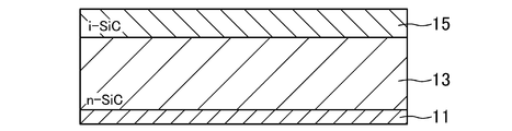
- the insulating heat conductive layer 15 made of i-type SiC is epitaxially grown on the + c plane of the drift layer 13.
- a region where the endothermic element portion 20 is not disposed is located above the electrode formation region 10a in the drift layer 13 which is a region where the cathode electrode 16 of the semiconductor element body portion 10 is formed.
- an insulating SiC having a thickness of about 1 ⁇ m is formed on the + c plane (hereinafter referred to as a surface) of the drift layer 13.
- a substrate on which the layer (thermal conductive layer 15) is epitaxially grown is prepared, and a nickel (Ni) film to be the anode electrode 11 is formed on the ⁇ c surface (hereinafter referred to as the back surface) of the prepared substrate.
- the substrate is washed with SH (sulfuric acid / hydrogen peroxide), and then a Ni film having a thickness of about 100 nm is formed on the back surface by sputtering.
- the substrate on which the Ni film is formed is put into a rapid thermal processing (RTA) furnace, and thermal processing is performed at a temperature of 1000 ° C. for 2 minutes.
- RTA rapid thermal processing
- the formed Ni film is silicided, that is, the anode electrode 11 made of nickel silicide (NiSi x ) is obtained.
- the substrate here may be a wafer-like substrate that can be divided into a plurality of chips, or a chip-like substrate that is divided into chips.
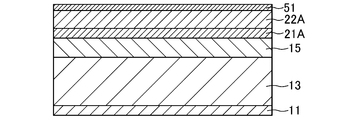
- a lower electrode formation film 21A made of nickel having a thickness of about 450 nm and a p-type silicon layer 22A having a thickness of about 1.2 ⁇ m are formed on the heat conductive layer 15, for example.
- a first sacrificial film 51 made of nickel having a thickness of about 200 nm is sequentially formed.
- the lower electrode formation film 21A and the first sacrificial film 51 can be formed by, for example, sputtering, and the p-type silicon layer 22A can be formed by, for example, chemical vapor deposition (CVD) or sputtering. .
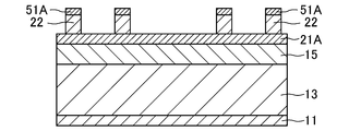
- a first mask pattern 61 for obtaining the dot-shaped p-type silicon layer 22 is formed from the p-type silicon layer 22A on the first sacrificial film 51 by lithography, and the first mask pattern thus formed is formed.
- the first sacrificial film 51 is wet-etched using hydrochloric acid overwater using 61 as a mask, thereby forming a first mask film 51A from the first sacrificial film 51 as shown in FIG.
- the hydrochloric acid overwater used here is a mixture in which the ratio of concentrated hydrochloric acid: hydrogen peroxide water: pure water is, for example, 1: 1: 10 by volume, and after adding pure water to the hydrogen peroxide water, Add concentrated hydrochloric acid.
- a plurality of p-type silicon layers 22 having a dot-like block pattern are obtained by dry etching using the formed first mask film 51A as a mask.
- dry etching inductively coupled plasma (ICP) using a mixed gas of chlorine (Cl 2 ) and hydrogen bromide (HBr) as a reactive gas is used.
- ICP inductively coupled plasma
- the substrate temperature is ⁇ 15 ° C.
- the pressure in the reactor is about 0.133 Pa
- the ICP output is 400 W
- the substrate bias voltage is 190 V.
- the flow rate of Cl 2 gas is 40 ml / min (0 ° C., 1 atm), and the flow rate of HBr gas is 20 ml / min (0 ° C., 1 atm). Note that the etching conditions are not limited to this.
- an n-type silicon layer 24 ⁇ / b> A and a second sacrificial film 52 made of nickel (Ni) are sequentially formed on the lower electrode formation film 21 ⁇ / b> A including the p-type silicon layer 22.
- the n-type silicon layer 24A can be formed by CVD or sputtering
- the second sacrificial film 52 can be formed by sputtering.
- a second mask film 52A for obtaining the dot-shaped n-type silicon layer 24 from the second sacrificial film 52 is formed using hydrochloric acid / hydrogen peroxide similar to the process shown in FIG. Form. Thereafter, the surface cleaning process of each second mask film 52 may be performed.
- the second mask film 52A is used as a mask, and ICP etching using a mixed gas of Cl 2 and HBr is used to form the n-type silicon layer 24A.
- a plurality of n-type silicon layers 24 having a dot-like block pattern are obtained.
- the order of forming the dot-shaped p-type silicon layer 22 and the n-type silicon 24 is not particularly limited.
- a second mask pattern 62 having an SBD electrode formation region 10a as an opening pattern is formed on the lower electrode formation film 21A including the p-type silicon layer 22 and the n-type silicon layer 24 by lithography. Subsequently, by using the formed second mask pattern 62 as a mask, the lower electrode formation film 21A is etched using hydrochloric acid / hydrogen peroxide to form electrodes in the lower electrode formation film 21A as shown in FIG. A portion included in the region 10a is removed.
- the second mask pattern 62 is removed, and then the first mask film 51A, the second mask film 52A, and the lower electrode formation film 21A are used as hard masks with respect to the heat conductive layer 15.
- ICP etching similar to the process shown in FIG. 11 is performed to expose the electrode formation region 10a of the drift layer 13.
- the value of the substrate bias voltage for ICP etching is set to, for example, 450 V from 190 V in the case of the silicon layer.
- the thickness of the lower electrode formation film 21A is 450 nm and the thickness of each of the mask films 51A and 52A is 200 nm.
- the thickness of the mask can be changed as appropriate.
- the thickness of the lower electrode formation film 21A may be about 700 nm at the maximum, and the thickness of each mask film 51A, 52A may be about 400 nm at the maximum.
- a third mask pattern 63 having a lower electrode formation pattern is formed on the lower electrode formation film 21A including the electrode formation region 10a of the drift layer 13 by lithography. Subsequently, using the formed third mask pattern 63 as a mask, etching is performed with hydrochloric acid overwater to form a plurality of lower electrodes 21 from the lower electrode formation film 21A.
- the third mask pattern 63 is removed, and subsequently, a silicon dioxide (SiO 2 ) dispersion is applied to the entire surface of the substrate by spin coating.
- a pre-curing process at a temperature of 180 ° C. for 30 minutes in air and a main curing process at a temperature of 400 ° C. for 30 minutes in nitrogen are sequentially performed to form the insulating film 23A.
- HMDS bis (trimethylsilyl) amine
- heat treatment of spin-coated HMDS in air at 180 ° C. for 5 minutes may be performed.
- a fourth mask pattern 64 having an opening pattern is formed in the electrode formation region 10a on the insulation formation film 23A by lithography, and the insulation formation film 23A is etched by wet etching using buffered hydrofluoric acid (BHF). Then, as shown in FIG. 16, the electrode formation region 10a in the drift layer 13 is exposed again.
- BHF buffered hydrofluoric acid
- an electrode forming film 25A made of nickel (Ni) is formed by sputtering so that the film thickness of at least the drift layer 13 on the electrode forming region 10a is, for example, 200 nm. To do. Thereafter, the surface of the electrode forming film 25A may be cleaned.
- a semiconductor element composed of an SBD element having the insulating (i-type SiC) heat conduction layer 15 epitaxially grown on the drift layer 13 which is a bulk portion of silicon carbide (SiC).
- a semiconductor device 100D having a main body portion 10 and a heat absorption element portion 20 formed of a thin Peltier element using silicon (Si) directly formed on the heat conductive layer 15, that is, thermally connected silicon (Si). Can be reliably formed.
- the insulating heat conductive layers 15 and 37 are made of i-type SiC. However, instead of this, all of them are insulating silicon (Si), gallium nitride ( GaN), aluminum nitride (AlN), silicon nitride (SiN x ), zinc oxide (ZnO), C (diamond), boron nitride (BN), or gallium oxide (Ga 2 O 3 ) may be used.
- the thermal conductivity of each constituent material is preferably 5 W / mK or more, and the resistivity is preferably 10 8 ⁇ cm or more.
- the heat conductive layers 15 and 37 made of these materials are integrated in contact with the semiconductor element body portions 10 and 30 in a thermal and continuous manner.
- the heat conduction layer made of these materials is formed by epitaxial growth from the surface of the semiconductor material constituting the semiconductor element body 10, 30.
- the semiconductor material constituting the semiconductor element body portions 10 and 30 includes silicon (Si), gallium nitride (GaN), aluminum nitride (AlN), silicon nitride (SiN x ), zinc oxide (ZnO), and C (diamond). ), Boron nitride (BN), or gallium oxide (Ga 2 O 3 ) can be used.
- the heat generation region (eg, the channel region 34a in FIG. 4) having a relatively narrow width in the semiconductor element body portions 10 and 30 and the heat insulating layer that insulates the periphery of the heat conductive layer 37 in FIG. A layer may be provided.
- the heat conductivity of the heat insulating layer is preferably 0.5 W / mK or less.
- a metal electrode 61 made of, for example, nickel is disposed on the front and back surfaces of a Peltier element 60, the front surface is connected to the positive electrode of the power source, and the back surface is connected to the negative electrode of the power source to pass a current I.
- the arrow 63 represents heat transfer due to the Peltier effect
- the arrow 64 represents heat transfer due to heat conduction
- the arrow 65 represents heat generation due to Joule heat.
- the temperature difference between the front and back surfaces of the Peltier element 60 is 40 ° C. This assumes, for example, a situation in which a cooler through which a cooling medium with a temperature of 80 ° C. flows is connected to the front side and a power device is connected to the back side, and the temperature of the power device is 120 ° C. or less. Can do.
- the ambient environment temperature is 295 K (22 ° C .: room temperature), and the electrical resistivity is 1 ⁇ 10 ⁇ 5 ⁇ m.
- the conventional bismuth tellurium and the lower limit value of this example are graphed in FIG. 20 and compared.
- the lowest value (referred to as need (N)) in the desired total heat transfer amount (endothermic amount) is set to 300 W / cm 2 in view of the application of the Peltier element of this embodiment. This is a need due to the amount of heat generated by the power device, for example.
- the maximum heat absorption amount is 308.8 W / cm 2 . Satisfy the above needs.
- the maximum heat absorption amount is only 23.4 W / cm 2 , and the above needs cannot be satisfied.
- FIG. 21 shows graphs of calculated values when the temperature difference ⁇ T between the front and back surfaces of each material (excluding bismuth tellurium) listed in [Table 1] is 40 ° C.
- the maximum heat absorption amount is about 3100 W / cm 2 . Accordingly, 10% or more of 3000 W / cm 2 which is 10 times the need N, that is, in this embodiment, if the Peltier element covers a region of 10% or more of the surface area of the power device which is a heat source, for example. The value of needs N can be satisfied.
- An endothermic element, a semiconductor device including the endothermic element, and a method for manufacturing the endothermic element according to the present invention can reduce the thermal resistance between the semiconductor element and the endothermic element, and are equipped with an inverter incorporating this type of semiconductor device (In addition to HV, HEV, etc.), power generation / transmission / distribution systems (smart grids, etc.), transport equipment other than automobiles (railways, ships, aircraft, etc.), industrial machinery (FA equipment, elevators, etc.), IT-related equipment (computers, mobile phones, etc.) It can be suitably applied in the field of consumer electronics / home appliances (air conditioners, FPDs, AV devices, etc.) and their manufacturing technology.
Landscapes
- Chemical & Material Sciences (AREA)
- Inorganic Chemistry (AREA)
- Engineering & Computer Science (AREA)
- Manufacturing & Machinery (AREA)
- Electrodes Of Semiconductors (AREA)
- Cooling Or The Like Of Semiconductors Or Solid State Devices (AREA)
Abstract
半導体素子本体部10の表面と電気絶縁体である熱伝導層15を介して熱的に接続されたペルチェ型で薄膜状の吸熱素子部20は、該吸熱素子部20を構成する物質における、バルクでの熱伝導率は50W/mK以上であり、ゼーベック係数は300μV/K以上である。
Description
本発明は、吸熱素子及びそれを備えた半導体装置並びに吸熱素子の製造方法に関する。
近年、パワー半導体装置からその外部への放熱性を高めるために、ペルチェ素子等の冷却素子を備えたパワー半導体装置が知られている。
従来のパワー半導体装置には、パワー半導体素子の発熱部とペルチェ素子とを近接してモジュール化した構成が知られている(例えば、特許文献1を参照。)。また、パワー半導体素子の発熱部に、具体的には、トレンチゲート電極同士の間の領域に、放熱用埋め込み金属を配置し、該放熱用埋め込み金属の上にペルチェ素子を設ける構成が知られている(例えば、特許文献2を参照。)。
しかしながら、上記の従来技術は、いずれも、パワー半導体素子の発熱部とペルチェ素子とを近接させてはいるものの、両者の接触部での熱抵抗が大きく、パワー半導体素子の発熱後、瞬時に冷却することができない。このため、現状では、パワー半導体素子に対する最大負荷時の発熱量に備えて、冗長で且つ高コストの熱設計をせざるを得ないという問題がある。
また、半導体素子上に形成される薄膜状のペルチェ素子の製造方法が確立されていないという問題も存在する。
本発明は、斯かる点に鑑みてなされたものであり、その課題とするところは、半導体素子の上に形成される薄膜状の吸熱素子において、半導体素子と吸熱素子との間の熱抵抗を低減できるようにすると共に、その製造方法を確立することにある。
上記の課題を解決するため、本発明は、半導体素子に形成するペルチェ型の吸熱素子を薄膜状に形成することを特徴とする。
具体的には、本発明は、吸熱素子及びそれを備えた半導体装置並びに吸熱素子の製造方法を対象とし、次のような解決手段を講じた。
すなわち、第1の発明は、半導体素子の表面と電気絶縁体を介して熱的に接続された、ペルチェ型で薄膜状の吸熱素子を対象とし、吸熱素子を構成する物質における、バルクでの熱伝導率は50W/mK以上であり、ゼーベック係数は300μV/K以上である。
これによれば、半導体素子と吸熱素子との間の熱抵抗を低減でき、半導体素子の放熱性を向上することができる。
第2の発明は、上記第1の発明において、上記の物質は、シリコン(Si)、炭化シリコン(SiC)、窒化ガリウム(GaN)、窒化アルミニウム(AlN)、窒化ボロン(BN)及びダイヤモンド(C)のうちのいずれか1つである。
これによれば、高効率な吸熱素子を確実に形成することができる。
第3の発明は、上記第1の発明において、上記の物質はシリコンである。
これによれば、半導体製造プロセスと馴染みやすいため好ましい。
第4の発明は、上記第1~第3の発明において、上記の物質は、p型又はn型の半導体層を構成し、p型半導体層及びn型半導体層は、半導体素子及び電気絶縁体に対して並行に配列されている。
これによれば、薄膜状の吸熱素子としてのペルチェ素子を確実に形成できると共に、半導体素子及び電気絶縁体との接触面積を大きくすることができ、吸熱効果(放熱効果)の効率が向上する。
第5の発明は、上記第1~第4の発明において、半導体素子の排熱側に直接に形成されて、熱的に連結されている。
これによれば、吸熱素子の吸熱効率が向上して半導体素子の放熱効果が良好となる。
第6の発明は、上記第1~第5の発明において、半導体素子における発熱源の面積の10%以上の領域を被覆している。
このように、発熱源の面積の10%以上を被覆していれば、半導体素子の放熱効果を向上することができる。
第7の発明は、請求項1~6の発明に係る吸熱素子を備える半導体装置である。
これによれば、本発明の半導体装置は、本発明の吸熱素子を備えているため、半導体素子の放熱性を向上することができる。
第8の発明は、上記第7の発明において、半導体素子はパワー半導体素子である。
これによれば、動作中に高温になるパワー半導体素子の放熱性を向上することができる。
第9の発明は、上記第7の発明において、半導体素子は、炭化シリコンを材料とするSiC系パワー半導体素子である。
これによれば、高耐圧、低オン抵抗及び高速動作可能なSiC系パワー半導体素子における放熱性を向上することができる。
第10の発明は、半導体素子の表面と電気絶縁体を介して熱的に接続された、ペルチェ型で薄膜状の吸熱素子の製造方法を対象とし、吸熱素子を形成する工程は、半導体素子の上に、電気絶縁体を介して、下部金属膜、第1導電型半導体層及び第1金属犠牲膜を順次形成する工程と、第1金属犠牲膜から第1導電型半導体層をパターニングする第1金属マスク膜を形成し、形成した第1金属マスク膜を用いて、第1導電型半導体層をパターニングすることにより、第1導電型半導体層から複数の第1導電型半導体ブロックを形成する工程と、第1導電型半導体ブロックを含む下部金属膜の上に、第2導電型半導体層及び第2金属犠牲膜を順次形成する工程と、第2金属犠牲膜から第2導電型半導体層をパターニングする第2金属マスク膜を形成し、形成した第2金属マスク膜を用いて、第2導電型半導体層をパターニングすることにより、第2導電型半導体層から複数の第2導電型半導体ブロックを形成する工程と、リソグラフィ法により、下部金属膜における半導体素子の電極形成領域に対して選択的にエッチングすることにより、半導体素子を露出する工程と、リソグラフィ法により、下部金属膜における第1導電型半導体ブロック及び第2導電型半導体ブロックの間を選択的にエッチングすることにより、下部金属膜から、複数の下部電極を形成する工程と、各半導体ブロックの間及び下部電極の間に絶縁膜を選択的に形成した後、各半導体素ブロックの上及び半導体素子の露出部分の上に、上部金属膜を形成する工程と、リソグラフィ法により、上部金属膜に対して選択的にエッチングを行うことにより、上部金属膜から、上部電極と半導体素子の電極とを形成する工程とを含む。
これによれば、吸熱素子が、半導体素子の上に電気絶縁体を介して形成された、吸熱素子の下部電極となる下部金属膜、第1導電型半導体層、第2導電型半導体層、並びに吸熱素子の下部電極及び半導体素子の電極となる上部金属膜をエッチングすることによって形成することができる。
第11の発明は、第10の発明において、第1導電型半導体層及び第2導電型半導体層は、シリコン(Si)、炭化シリコン(SiC)、窒化ガリウム(GaN)、窒化アルミニウム(AlN)、窒化ボロン(BN)及びダイヤモンド(C)のうちのいずれか1つである。
これによれば、高効率な吸熱素子を確実に形成することができる。
第12の発明は、第10又は第11の発明において、下部金属膜、第1金属犠牲膜、第2金属犠牲膜及び上部金属膜はニッケルからなり、下部金属膜、第1金属犠牲膜、第2金属犠牲膜及び上部金属膜の少なくとも1つに対するパターニングには、濃塩酸、濃過酸化水素水及び純水の混合物(塩酸過水)をエッチャントとするウェットエッチングを用いる。
これによれば、レジストを劣化させることなく、ニッケル膜をエッチングすることができる。
第13の発明は、第10~第12の発明において、第1金属犠牲膜及び第2金属犠牲膜はニッケルからなり、第1導電型半導体層及び第2導電型半導体層はシリコンからなり、第1導電型半導体ブロック及び第2導電型半導体ブロックを形成する工程は、塩素と臭化水素とを用いるドライエッチングである。
これによれば、シリコンからなる第1導電型半導体層及び第2導電型半導体層から第1導電型半導体ブロック及び第2導電型半導体ブロックを形成するエッチングを行う際に、ニッケルからなる第1金属マスク膜となる第1金属犠牲膜及び第2金属マスク膜となる 第2金属犠牲膜をハードマスクとして用いることができる。
第14の発明は、第10~第13の発明において、半導体素子はパワー半導体素子である。
これによれば、動作中に高温になるパワー半導体素子の放熱性を向上することができる。
第15の発明は、第10~第13の発明において、半導体素子は、炭化シリコンを材料とするSiC系パワー半導体素子である。
これによれば、高耐圧、低オン抵抗及び高速動作可能なSiC系パワー半導体素子における放熱性を向上することができる。
本発明によれば、半導体素子と吸熱素子との間の熱抵抗を大幅に低減することができると共に、半導体素子の表面に形成する薄膜状の吸熱素子を確実に形成することができる。
以下、本発明の実施形態を図面に基づいて詳細に説明する。以下の好ましい実施形態の説明は、本質的に例示に過ぎず、本発明、その適用物又はその用途を制限することを意図しない。
(第1の実施形態)
図1は本発明の第1の実施形態に係る半導体装置の要部の断面構成を示している。
図1は本発明の第1の実施形態に係る半導体装置の要部の断面構成を示している。
図1に示すように、本実施形態に係る半導体装置100は、半導体素子本体部10と、該半導体素子本体部10の上に一体に形成された吸熱素子部20とから構成される。
半導体素子本体部10は、ショットキーバリアダイオード(以下、SBDとも略称する。)であり、該ダイオードを構成する半導体には、例えば、炭化シリコン(SiC)を用いることができる。ここでは、半導体素子本体部10は、例えば、n+型SiCからなるバルク層(コンタクト層)12と、該バルク層12の上にエピタキシャル成長したn型SiCからなり、耐圧を規制するドリフト層13と、該ドリフト層13の上にエピタキシャル成長したi型SiCからなる絶縁性の熱伝導層15と、バルク層12におけるドリフト層13と反対側の面(裏面)上に形成されたアノード電極11と、ドリフト層13におけるバルク層12と反対側の面(表面)上で、且つ、熱伝導層15から部分的に露出された領域(電極形成領域)の上に選択的に形成された複数のカソード電極16とから構成される。図1においては、便宜上、複数のカソード電極16のうちの1つを図示しているが、同一形状の複数のカソード電極16が横方向に(2次元的に)所定の間隔をおいて配置されている。ここでは、アノード電極11として、例えば、ニッケルシリサイド(NiSix)を用い、カソード電極16として、ニッケル(Ni)を用いている。また、ドリフト層13の上部におけるカソード電極16と対向する周縁部には、該SBDの耐圧を向上させるためのp+領域14が形成されている。なお、該p+領域14は、当該SBDに必ずしも設ける必要はなく、半導体装置100の用途等に応じて適宜設ければよい。
アノード電極11の構成材料は、ニッケルシリサイドに限られず、n型SiCと良好なオーミック接触を得られる金属又は金属シリサイドであれば適用できる。また、カソード電極16の構成材料は、ニッケルに限られず、n型SiCと良好なショットキー接触を得られる金属であれば適用できる。
一方、吸熱素子部20は、半導体素子本体部10の上に、それぞれ複数のドット(島)状に交互に配置されたp型シリコン層22及びn型シリコン層24と、これらシリコン層22、24に交互に電流が流れるようにその下部に配置された下部電極21及びその上部に配置された上部電極25とから構成された薄膜状のペルチェ素子である。ここで、下部電極21及び上部電極25には、例えば、ニッケル(Ni)を用いることができる。p型シリコン層22及びn型シリコン層24との間、下部電極21同士の間並びに上部電極25同士の間には、例えば酸化シリコン(SiO2)からなる絶縁膜23が充填されて形成されている。
吸熱素子部20は、その下部電極21が、半導体素子本体部10の表面から露出するi型SiCからなる絶縁性の熱伝導層15と直接に接続、すなわち熱的に連結されている。また、カソード電極16の上方の領域において、吸熱素子部20は、カソード電極16の周囲に充填された、例えば酸化シリコン(SiO2)からなる絶縁膜17と接続されている。このように、p型シリコン層22及びn型シリコン層24は、半導体素子本体部10の熱伝導層15と絶縁膜17とに対して並行に配列されている。
なお、吸熱素子部20を構成する半導体として、シリコン(Si)を用いたが、これに限られず、該シリコン(Si)と同様に、バルクでの熱伝導率が50W/mK以上であり、ゼーベック係数が300μV/K以上である半導体材料を用いることができる。そのような半導体材料には、例えば、炭化シリコン(SiC)、窒化ガリウム(GaN)、窒化アルミニウム(AlN)、窒化ボロン(BN)又はダイヤモンド(C)等がある。これらを用いると、高効率のペルチェ素子を作製することができる。
また、下部電極21及び上部電極25には、ニッケル(Ni)を用いたが、これに限られず、チタン(Ti)、アルミニウム(Al)、錫(Sn)、モリブデン(Mo)、銅(Cu)又は金(Au)を用いることができる。
本実施形態においては、下部電極21は、例えば厚さが450nmのNi膜とし、p型シリコン層22及びn型シリコン層24は、例えば厚さを1.2μmとし、上部電極25は、例えば厚さが200nmのNi膜としている。このように、本実施形態に係る半導体装置100を構成する吸熱素子部20の本体の厚さは1.85μmであり、2μm以内に収まる。
また、吸熱素子部20は、半導体素子本体部10における発熱源の面積の10%以上の領域を被覆していれば、本発明の効果を確実に得ることができる。ここで、半導体素子本体部10の発熱源とは、主として、ドリフト層13における複数のカソード電極16とアノード電極11との対向部分を含む領域の平面視での領域の総和をいう。
-効果-
以上より、本実施形態によれば、SBDとして構成された半導体素子本体部10の上に一体に形成される薄膜状のペルチェ型の吸熱素子部20において、該吸熱素子部20の下部電極21が、半導体素子本体部10のエピタキシャル成長部である絶縁性の熱伝導層15と直接に接続される。このため、半導体素子本体部10と吸熱素子部20との間の熱抵抗が大幅に低減される。
以上より、本実施形態によれば、SBDとして構成された半導体素子本体部10の上に一体に形成される薄膜状のペルチェ型の吸熱素子部20において、該吸熱素子部20の下部電極21が、半導体素子本体部10のエピタキシャル成長部である絶縁性の熱伝導層15と直接に接続される。このため、半導体素子本体部10と吸熱素子部20との間の熱抵抗が大幅に低減される。
(第1の実施形態の第1変形例)
図2は本発明の第1の実施形態の第1変形例に係る半導体装置の要部の断面構成を示している。
図2は本発明の第1の実施形態の第1変形例に係る半導体装置の要部の断面構成を示している。
第1変形例に係る半導体装置100Aは、半導体素子本体部10が第1の実施形態と異なっているが、その他の点については、第1の実施形態と同様の構成である。そこで、以下の説明では、第1の実施形態の構成要素と同様の構成要素については、同一の符号を付している。
図2に示すように、本変形例に係る半導体装置100Aに含まれる半導体素子本体部10は、ジャンクションバリアショットキーダイオード(以下、JBSダイオードとも略称する。)である。半導体素子本体部10を構成するJBSダイオードは、i型SiCからなる絶縁性の熱伝導層15に、互いに間隔をおいた複数の空隙部を設け、この空隙部に、例えばニッケル(Ni)を充填してなる複数のカソード電極16aを有している。
また、ドリフト層13における分割された各熱伝導層15の下側部分には、それぞれ、p+領域14aが形成されて、半導体素子本体部10の耐圧を向上させている。
なお、吸熱素子部20においては、第1の実施形態と同等の構成である。
従って、第1の実施形態で説明した部材の厚さ等だけでなく、他の適用可能な材料は、本変形例においても適用できる。
(第1の実施形態の第2変形例)
図3は本発明の第1の実施形態の第2変形例に係る半導体装置の要部の断面構成を示している。
図3は本発明の第1の実施形態の第2変形例に係る半導体装置の要部の断面構成を示している。
第2変形例に係る半導体装置100Bは、半導体素子本体部10が第1変形例と異なっているが、その他の点については、第1変形例と同様の構成である。そこで、図3においても、図2の構成要素と同様の構成要素については、同一の符号を付している。
図3に示すように、本変形例に係る半導体装置100Bに含まれる半導体素子本体部10は、第1変形例に係るJBSダイオードから、耐圧向上のためのp+領域14aを省略している。従って、第2変形例に係るJBSダイオードは、ショットキーバリアダイオード(SBD)である。これは、ドリフト層13に、耐圧が高いn型SiCを用いていることから、p+領域14aを省略した場合でも、SBDとして動作が可能となるからである。
また、本変形例においても、第1の実施形態で説明した部材の厚さ等に加え、他の適用可能な材料も適用できる。
(第2の実施形態)
図4は本発明の第2の実施形態に係る半導体装置の要部の断面構成を示している。
図4は本発明の第2の実施形態に係る半導体装置の要部の断面構成を示している。
図4に示すように、本実施形態に係る半導体装置100Cは、半導体素子本体部30と、該半導体素子本体部30の上に一体に形成された吸熱素子部20とから構成される。
第2の実施形態に係る半導体装置100Cは、半導体素子本体部10が第1の実施形態と異なっているが、その他の点については、第1の実施形態と同様の構成である。そこで、以下の説明では、第1の実施形態の構成要素と同様の構成要素については、同一の符号を付している。
図4に示すように、本実施形態に係る半導体装置100Cに含まれる半導体素子本体部30は、金属-酸化物-半導体電界効果トランジスタ(以下、MOSFETとも略称する。)である。半導体素子本体部30を構成するMOSFETは、n+型SiCからなるバルク層(コンタクト層)32と、該バルク層32の上にエピタキシャル成長したn型SiCからなり、耐圧を規制するドリフト層33と、該ドリフト層33の上にエピタキシャル成長したi型SiCからなる絶縁性の熱伝導層37とを有している。ここでは、n+型SiCの不純物濃度は、例えば、1.0×1018cm-3程度としてもよく、n型SiCは、1.0×1016cm-3程度としてもよい。また、ドリフト層33の厚さは、10μm程度としてもよい。
ドリフト層33の表面上で、且つ、熱伝導層37から部分的に露出された領域(電極形成領域)の上には、ゲート絶縁膜38aを介したゲート電極39が選択的に形成されている。該ゲート電極39及びゲート絶縁膜38aは、絶縁膜38bにより覆われている。ここで、ゲート電極39には、例えば、多結晶シリコン(Poly-Si)でもよく、さらには、多結晶炭化シリコン(Poly-SiC)、アルミニウム(Al)又は銅(Cu)を用いてもよい。また、ゲート絶縁膜38aには、例えば、酸化シリコン(SiO2)でもよく、さらには、酸化アルミニウム(Al2O3)、窒化アルミニウム(AlN)、窒化シリコン(Si3N4)、窒化ボロン(BN)又はダイヤモンド(C)を用いてもよい。
さらに、ドリフト層33の上で、且つ熱伝導層37同士の間の電極形成領域には、例えばニッケル(Ni)からなるソース電極40が絶縁膜38bを覆うように形成されている。
ドリフト層33の上部には、各熱伝導層37とこれと対向するゲート絶縁膜38aの端部との間に、それぞれp型のボディ層34が形成されている。さらに、各ボディ層34の上部には、ゲート絶縁膜38a側にn+型のソース層35がそれぞれ形成され、該ソース層35と隣接して熱伝導層37側に、耐圧向上のためのp+領域36がそれぞれ形成されている。各ソース層35は、その上に形成されているソース電極40とオーミック接触する。なお、バルク層32の裏面上には、例えばニッケル(Ni)からなるドレイン電極31が形成されている。これらボディ層34、ソース層35及びp+領域36は、それぞれ、公知のリソグラフィ法及びイオン注入法等によって形成することができる。ここで、ボディ層34のp型の不純物濃度は、例えば、1.0×1016cm-3程度としてもよく、また、ソース層35のn型の不純物濃度は、例えば、1.0×1020cm-3程度としてもよい。
MOSFETにおいては、ゲート電極39に所定の電圧が引加されて、p型のボディ層34におけるゲート絶縁膜38aとの境界部分に反転層であるn型のチャネル領域34aが形成される。その結果、動作電流は、ドレイン電極31、バルク層32、ドリフト層33、チャネル領域34a、ソース層35及びソース電極40の順に流れる。この電流経路においては、チャネル領域34aにおけるチャネル抵抗とドリフト層33におけるドリフト抵抗とが大きい。従って、該チャネル抵抗及び該ドリフト抵抗によるジュール熱が、半導体素子本体部30の全体の発熱量に占める割合が高い。
ここでも、第1の実施形態の半導体装置100と同様に、吸熱素子部20は、半導体素子本体部30における発熱源の面積の10%以上の領域を被覆していれば、本発明の効果を確実に得ることができる。半導体素子本体部30の発熱源とは、上記の説明から、主として、複数のチャネル領域34aとドリフト層33を含む領域の平面視での領域の総和をいう。
-効果-
以上より、本実施形態によれば、MOSFETとして構成された半導体素子本体部30の上に一体に形成される薄膜状のペルチェ型の吸熱素子部20において、該吸熱素子部20の下部電極21が、半導体素子本体部30のエピタキシャル成長部である絶縁性の熱伝導層37と直接に接続される。このため、半導体素子本体部30と吸熱素子部20との間の熱抵抗が大幅に低減される。
以上より、本実施形態によれば、MOSFETとして構成された半導体素子本体部30の上に一体に形成される薄膜状のペルチェ型の吸熱素子部20において、該吸熱素子部20の下部電極21が、半導体素子本体部30のエピタキシャル成長部である絶縁性の熱伝導層37と直接に接続される。このため、半導体素子本体部30と吸熱素子部20との間の熱抵抗が大幅に低減される。
(第3の実施形態)
以下、本発明の第3の実施形態に係る半導体装置の製造方法の一例について図面を参照しながら説明する。図5~図18は第3の実施形態に係る半導体装置の要部の製造方法の工程順の断面構成を示している。
以下、本発明の第3の実施形態に係る半導体装置の製造方法の一例について図面を参照しながら説明する。図5~図18は第3の実施形態に係る半導体装置の要部の製造方法の工程順の断面構成を示している。
まず、図18に示す第3の実施形態に係る半導体装置100Dを構成する半導体素子本体部10は、バルク層がn型SiCからなるドリフト層13として構成されている。また、i型SiCからなる絶縁性の熱伝導層15は、ドリフト層13の+c面上にエピタキシャル成長されて形成されている。また、半導体素子本体部10のカソード電極16を形成する領域であるドリフト層13における電極形成領域10aの上方は、吸熱素子部20が配置されない領域となっている。
本実施形態に係る半導体装置100Dの製造方法は、まず、図5に示すように、ドリフト層13の+c面(以下、表面と呼ぶ。)の上に、厚さが1μm程度の絶縁性のSiC層(熱伝導層15)がエピタキシャル成長された基板を用意し、用意した基板の-c面(以下、裏面と呼ぶ。)上に、アノード電極11となるニッケル(Ni)膜を成膜する。具体的には、基板をSH(硫酸過水)洗浄し、その後、スパッタ法により、裏面の上に、厚さが100nm程度のNi膜を成膜する。続いて、Ni膜が成膜された基板を高速熱処理(RTA)炉に投入して、温度が1000℃で2分間の熱処理を行う。この熱処理により、成膜されたNi膜はシリサイド化され、すなわちニッケルシリサイド(NiSix)からなるアノード電極11を得る。なお、ここでの基板は、複数のチップに分割できるウェーハ状態の基板でもよく、チップに分割されたチップ状の基板であってもよい。
次に、図6に示すように、熱伝導層15の上に、例えば、厚さが450nm程度のニッケルからなる下部電極形成膜21Aと、厚さが1.2μm程度のp型シリコン層22Aと、厚さが200nm程度のニッケルからなる第1犠牲膜51とを順次形成する。下部電極形成膜21A及び第1犠牲膜51は、例えばスパッタ法により成膜することができ、p型シリコン層22Aは、例えば化学気相堆積(CVD)法又はスパッタ法により成膜することができる。
次に、リソグラフィ法により、第1犠牲膜51の上に、p型シリコン層22Aから、ドット状のp型シリコン層22を得るための第1マスクパターン61を形成し、形成した第1マスクパターン61をマスクとし、塩酸過水を用いて、第1犠牲膜51をウェットエッチングすることにより、図7に示すように、第1犠牲膜51から第1マスク膜51Aを形成する。ここで用いた塩酸過水は、濃塩酸:過酸化水素水:純水の比率が、例えば、体積比で1:1:10とした混合物であり、過酸化水素水に純水を加えた後に、濃塩酸を加える。
次に、図8に示すように、形成された第1マスク膜51Aをマスクとしたドライエッチングにより、ドット状のブロックパターンを有する複数のp型シリコン層22を得る。ドライエッチングには、塩素(Cl2)と臭化水素(HBr)との混合ガスを反応性ガスとする誘導結合プラズマ(ICP)を用いている。プラズマエッチング条件の一例として、基板温度を-15℃、反応器内圧力を約0.133Pa、ICP出力を400W、基板バイアス電圧を190Vとしている。また、Cl2ガスの流量は40ml/min(0℃、1atm)とし、HBrガスの流量は20ml/min(0℃、1atm)としている。なお、エッチング条件は、これに限られない。
次に、図9から図11に示す工程においては、ドット状のブロックパターンを有する複数のn型シリコン層24を形成する。
ずなわち、図9に示すように、p型シリコン層22を含む下部電極形成膜21Aの上に、n型シリコン層24A及びニッケル(Ni)からなる第2犠牲膜52を順次形成する。ここでも、n型シリコン層24AはCVD法又はスパッタ法により、第2犠牲膜52はスパッタ法により成膜することができる。
次に、図10に示すように、図7に示す工程と同様の塩酸過水を用いて、第2犠牲膜52から、ドット状のn型シリコン層24を得るための第2マスク膜52Aを形成する。この後、各第2マスク膜52の表面清浄化処理を行ってもよい。
次に、図11に示すように、図8に示す工程と同様に、第2マスク膜52Aをマスクとし、Cl2とHBrとの混合ガスを用いたICPエッチングにより、n型シリコン層24Aから、ドット状のブロックパターンを有する複数のn型シリコン層24を得る。なお、ドット状のp型シリコン層22及びn型シリコン24の形成順序は、特に問われない。
次に、リソグラフィ法により、p型シリコン層22及びn型シリコン層24を含む下部電極形成膜21Aの上に、SBDの電極形成領域10aを開口パターンに持つ第2マスクパターン62を形成する。続いて、形成された第2マスクパターン62をマスクとして、下部電極形成膜21Aに対して塩酸過水を用いたエッチングを行うことにより、図12に示すように、下部電極形成膜21Aにおける電極形成領域10aに含まれる部分を除去する。
次に、図13に示すように、第2マスクパターン62を除去し、続いて、第1マスク膜51A、第2マスク膜52A及び下部電極形成膜21Aをハードマスクとして、熱伝導層15に対して、図11に示す工程と同様のICPエッチングを行って、ドリフト層13の電極形成領域10aを露出する。ここでは、i型SiCからなる熱伝導層15の厚さを1μmとしているため、ICPエッチングの基板バイアス電圧の値をシリコン層の場合の190Vから、例えば450Vとしている。本実施形態においては、上述のように、下部電極形成膜21Aの膜厚を450nmとし、各マスク膜51A、52Aの膜厚を200nmとしているが、ハードマスクの目減り分を考慮して、各ハードマスクの厚さは適宜変更が可能である。例えば、本実施形態の場合は、下部電極形成膜21Aの膜厚を最大で700nm程度とし、各マスク膜51A、52Aの膜厚を最大で400nm程度としてもよい。
次に、図14に示すように、リソグラフィ法により、ドリフト層13の電極形成領域10aを含む下部電極形成膜21Aの上に、下部電極形成パターンを有する第3マスクパターン63を形成する。続いて、形成した第3マスクパターン63をマスクとして、塩酸過水によりエッチングを行って、下部電極形成膜21Aから複数の下部電極21を形成する。
次に、図15に示すように、第3マスクパターン63を除去し、続いて、スピンコート法により、基板上の全面に二酸化シリコン(SiO2)分散液を塗布する。続いて、空気中で温度が180℃、30分間の前硬化処理と、窒素中で温度が400℃、30分間の本硬化処理とを順次行って、絶縁形成膜23Aを成膜する。なお、絶縁形成膜23Aを成膜するよりも前に、各シリコン22、24の表面及びドリフト層13における電極形成領域10aの表面の疎水化を図るために、例えば、ビス(トリメチルシリル)アミン(HMDS)による熱処理を施してもよい。具体的には、スピンコートしたHMDSを空気中で温度が180℃、5分間の熱処理を行うとよい。
次に、リソグラフィ法により、絶縁形成膜23A上における電極形成領域10aに開口パターンを有する第4マスクパターン64を形成し、バッファードフッ酸(BHF)を用いたウェットエッチングにより絶縁形成膜23Aをエッチングして、図16に示すように、ドリフト層13における電極形成領域10aを再度露出する。
次に、図17に示すように、スパッタ法により、少なくともドリフト層13の電極形成領域10a上での膜厚が、例えば200nmとなるように、ニッケル(Ni)からなる電極形成膜25Aを成膜する。この後、電極形成膜25Aの表面の清浄化処理を行ってもよい。
次に、図18に示すように、リソグラフィ法により、電極形成膜25Aの上に、ペルチェ素子の上部電極パターン及びSBDの電極パターンを有するマスクパターン(図示せず)を用いて、塩酸過水によるウェットエッチングを行って、電極形成膜25Aから、ペルチェ素子の複数の上部電極25と、SBDのカソード電極16をそれぞれ形成する。これにより、本実施形態に係る半導体装置100Dを得る。
-効果-
以上より、本実施形態によれば、例えば、炭化シリコン(SiC)のバルク部であるドリフト層13の上にエピタキシャル成長した絶縁性(i型SiC)の熱伝導層15を有するSBD素子からなる半導体素子本体部10と、該熱伝導層15の上に直接に形成された、すなわち熱的に連結されたシリコン(Si)を用いた薄膜状のペルチェ素子からなる吸熱素子部20とを有する半導体装置100Dを確実に形成することができる。
以上より、本実施形態によれば、例えば、炭化シリコン(SiC)のバルク部であるドリフト層13の上にエピタキシャル成長した絶縁性(i型SiC)の熱伝導層15を有するSBD素子からなる半導体素子本体部10と、該熱伝導層15の上に直接に形成された、すなわち熱的に連結されたシリコン(Si)を用いた薄膜状のペルチェ素子からなる吸熱素子部20とを有する半導体装置100Dを確実に形成することができる。
(その他の実施形態)
上記の各実施形態及びその変形例においては、絶縁性の熱伝導層15、37は、i型SiCにより構成したが、これに代えて、いずれも絶縁性の、シリコン(Si)、窒化ガリウム(GaN)、窒化アルミニウム(AlN)、窒化シリコン(SiNx)、酸化亜鉛(ZnO)、C(ダイヤモンド)、窒化ボロン(BN)又は酸化ガリウム(Ga2O3)を用いてもよい。ここで、各構成材料の熱伝導率は、5W/mK以上、且つ、抵抗率が108Ωcm以上であることが好ましい。
上記の各実施形態及びその変形例においては、絶縁性の熱伝導層15、37は、i型SiCにより構成したが、これに代えて、いずれも絶縁性の、シリコン(Si)、窒化ガリウム(GaN)、窒化アルミニウム(AlN)、窒化シリコン(SiNx)、酸化亜鉛(ZnO)、C(ダイヤモンド)、窒化ボロン(BN)又は酸化ガリウム(Ga2O3)を用いてもよい。ここで、各構成材料の熱伝導率は、5W/mK以上、且つ、抵抗率が108Ωcm以上であることが好ましい。
また、これらの材料からなる熱伝導層15、37は、半導体素子本体部10、30に対して、熱的に且つ連続的に接触して一体化されていることが好ましい。
また、これらの材料からなる熱伝導層は、半導体素子本体部10、30を構成する半導体材料の表面からエピタキシャル成長して形成されていることが好ましい。
すなわち、半導体素子本体部10、30を構成する半導体材料には、シリコン(Si)、窒化ガリウム(GaN)、窒化アルミニウム(AlN)、窒化シリコン(SiNx)、酸化亜鉛(ZnO)、C(ダイヤモンド)、窒化ボロン(BN)又は酸化ガリウム(Ga2O3)を用いることができる。
また、半導体素子本体部10、30における幅が比較的に狭い発熱領域(例えば、図4のチャネル領域34a)、及び例えば、図4の熱伝導層37の長手方向にわたって、その周囲を断熱する断熱層が設けられていてもよい。この場合の断熱層の熱伝導率は、0.5W/mK以下であることが好ましい。
以下、本発明に係る吸熱素子の一実施例について図面を参照しながら説明する。
図19に示すように、本実施例に係る吸熱素子であるペルチェ素子60は、その単体の大きさを、平面積S×高さ(厚さ)l=1mm2×1mm=1mm3とする。図19において、ペルチェ素子60の表面及び裏面に、例えばニッケルからなる金属電極61を配置し、その表面を電源の正極と接続し、その裏面を電源の負極と接続して電流Iを流す。このとき、矢印63はペルチェ効果による熱移動を表し、矢印64は熱伝導による熱移動を表し、矢印65はジュール熱による発熱を表す。
ここでは、ペルチェ素子60の表裏面の温度差を40℃とする。これは、例えば、表面側に温度が80℃の冷却媒体が流通する冷却器が接続され、裏面側にパワーデバイスが接続されて、該パワーデバイスの温度が120℃以下となる状況を想定することができる。周囲環境温度は295K(22℃:室温)とし、電気抵抗率は、1×10⁻⁵Ωmとする。
以下に、ペルチェ素子の吸熱性能を表す導出式として一般的な[式1]を記す。
[式1]
Qout = αeTcjI -(1/2)RI2 -KΔTj
但し、R = ρ(S/l), K = κ(l/S)
ここで、Qoutは総熱移動量、αはゼーベック係数、Tは室温、Iは電流(ペルチェ駆動電流)、ΔTは表裏面温度差、ρは電気抵抗率、Sはペルチェ素子の単体面積、lはペルチェ素子の単体厚さ、κは熱伝導率をそれぞれ表す。また、[式1]の第1項は、ペルチェ効果を表し、第2項はジュール熱を表し、第3項は熱伝導を表す。
[式1]
Qout = αeTcjI -(1/2)RI2 -KΔTj
但し、R = ρ(S/l), K = κ(l/S)
ここで、Qoutは総熱移動量、αはゼーベック係数、Tは室温、Iは電流(ペルチェ駆動電流)、ΔTは表裏面温度差、ρは電気抵抗率、Sはペルチェ素子の単体面積、lはペルチェ素子の単体厚さ、κは熱伝導率をそれぞれ表す。また、[式1]の第1項は、ペルチェ効果を表し、第2項はジュール熱を表し、第3項は熱伝導を表す。
以下の[表1]に、従来から使用されているビスマステルル(Bi2Te3)、並びに本発明に使用可能なシリコン(Si)、炭化シリコン(SiC)、窒化ガリウム(GaN)、窒化アルミニウム(AlN)、窒化ボロン(BN)及びダイヤモンド(C)のそれぞれの計算に用いる数値の一覧を記す。
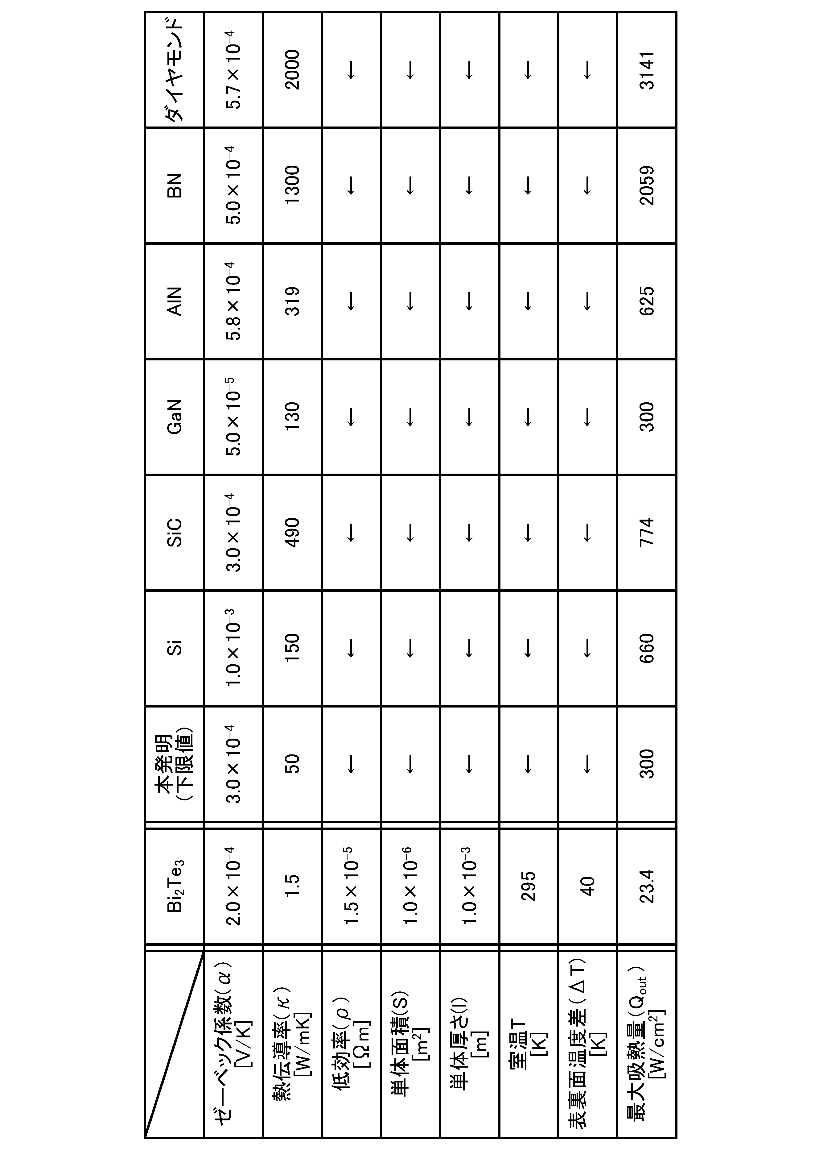
次に、[表1]の数値による[式1]の計算結果から、従来のビスマステルルと本実施例(本発明)の下限値とを図20にグラフ化して両者を比較する。本実施例においては、所望の総熱移動量(吸熱量)における最低値(ニーズ(N)と呼ぶ。)を本実施例のペルチェ素子の用途に鑑み、300W/cm2に設定する。これは、例えばパワーデバイスの発熱量によるニーズである。
図20に示すように、本実施例に係る下限値を表すグラフA(ゼーベック係数が300μV/K以上且つ熱伝導率が50W/mK以上)では、その最大吸熱量が308.8W/cm2となり、上記のニーズを満たす。一方、グラフBに示すビスマステルルを用いた従来のペルチェ素子の場合は、その最大吸熱量が23.4W/cm2に過ぎず、上記のニーズを満たすことはできない。
図21に、[表1]に掲載した各材料(ビスマステルルを除く)における表裏面の温度差ΔTを40℃とした場合の計算値によるグラフをそれぞれ示す。図21に示すように、ペルチェ素子の構成材料にダイヤモンドを用いたグラフCにおいて、その最大吸熱量は3100W/cm2程度を示す。従って、ニーズNの10倍の3000W/cm2の10%以上、すなわち、本実施例においては、ペルチェ素子が、例えば発熱源であるパワーデバイスの表面積の10%以上の領域を被覆していれば、ニーズNの値を満たすことが可能となる。
本発明に係る吸熱素子及びそれを備えた半導体装置並びに吸熱素子の製造方法は、半導体素子と吸熱素子との間の熱抵抗を低減でき、この種の半導体装置を組み込んだインバータを搭載した自動車(HV、HEV等)に加え、発電・送配電システム(スマートグリッド等)、自動車以外の輸送機器(鉄道、船舶、航空機等)、産業機械(FA機器、エレベータ等)、IT関連機器(パソコン、携帯電話等)及び民生・家電機器(エアコン、FPD、AV機器等)並びにそれらの製造技術分野において好適に適用できる。
10 半導体素子本体部(半導体素子/パワー半導体素子)
10a 電極形成領域
15 熱伝導層(電気絶縁体)
16 カソード電極(半導体素子の電極)
16a カソード電極
20 吸熱素子部(吸熱素子/ペルチェ素子)
21A 下部電極形成膜(下部金属膜)
21 下部電極
22 p型シリコン層(p型半導体層/第1導電型半導体ブロック)
22A p型シリコン層(第1導電型半導体層)
24 n型シリコン層(n型半導体層/第2導電型半導体ブロック)
24A n型シリコン層(第2導電型半導体層)
25 上部電極
25A 電極形成膜(上部金属膜)
30 半導体素子本体部(半導体素子/パワー半導体素子)
51 第1犠牲膜(第1金属犠牲膜)
51A 第1マスク膜(第1金属マスク膜)
52 第2犠牲膜(第2金属犠牲膜)
52A 第2マスク膜(第2金属マスク膜)
60 ペルチェ素子
100、100A、100B、100C、100D 半導体装置
10a 電極形成領域
15 熱伝導層(電気絶縁体)
16 カソード電極(半導体素子の電極)
16a カソード電極
20 吸熱素子部(吸熱素子/ペルチェ素子)
21A 下部電極形成膜(下部金属膜)
21 下部電極
22 p型シリコン層(p型半導体層/第1導電型半導体ブロック)
22A p型シリコン層(第1導電型半導体層)
24 n型シリコン層(n型半導体層/第2導電型半導体ブロック)
24A n型シリコン層(第2導電型半導体層)
25 上部電極
25A 電極形成膜(上部金属膜)
30 半導体素子本体部(半導体素子/パワー半導体素子)
51 第1犠牲膜(第1金属犠牲膜)
51A 第1マスク膜(第1金属マスク膜)
52 第2犠牲膜(第2金属犠牲膜)
52A 第2マスク膜(第2金属マスク膜)
60 ペルチェ素子
100、100A、100B、100C、100D 半導体装置
Claims (15)
- 半導体素子の表面と電気絶縁体を介して熱的に接続された、ペルチェ型で薄膜状の吸熱素子であって、
前記吸熱素子を構成する物質における、バルクでの熱伝導率は50W/mK以上であり、ゼーベック係数は300μV/K以上であることを特徴とする吸熱素子。 - 請求項1に記載の吸熱素子において、
前記物質は、シリコン、炭化シリコン、窒化ガリウム、窒化アルミニウム、窒化ボロン及びダイヤモンドのうちのいずれか1つであることを特徴とする吸熱素子。 - 請求項1に記載の吸熱素子において、
前記物質は、シリコンであることを特徴とする吸熱素子。 - 請求項1~3のいずれか1項に記載の吸熱素子において、
前記物質は、p型又はn型の半導体層を構成し、
前記p型半導体層及び前記n型半導体層は、前記半導体素子及び前記電気絶縁体に対して並行に配列されていることを特徴とする吸熱素子。 - 請求項1~4のいずれか1項に記載の吸熱素子において、
前記半導体素子の排熱側に直接に形成されて、熱的に連結されていることを特徴とする吸熱素子。 - 請求項1~5のいずれか1項に記載の吸熱素子において、
前記半導体素子における発熱源の面積の10%以上の領域を被覆していることを特徴とする吸熱素子。 - 請求項1~6のいずれか1項に記載の吸熱素子を備える半導体装置。
- 請求項7に記載の半導体装置において、
前記半導体素子は、パワー半導体素子であることを特徴とする半導体装置。 - 請求項7に記載の半導体装置において、
前記半導体素子は、炭化シリコンを材料とするSiC系パワー半導体素子であることを特徴とする半導体装置。 - 半導体素子の表面と電気絶縁体を介して熱的に接続された、ペルチェ型で薄膜状の吸熱素子の製造方法であって、
前記吸熱素子を形成する工程は、
前記半導体素子の上に、前記電気絶縁体を介して、下部金属膜、第1導電型半導体層及び第1金属犠牲膜を順次形成する工程と、
前記第1金属犠牲膜から前記第1導電型半導体層をパターニングする第1金属マスク膜を形成し、形成した前記第1金属マスク膜を用いて、前記第1導電型半導体層をパターニングすることにより、前記第1導電型半導体層から複数の第1導電型半導体ブロックを形成する工程と、
前記第1導電型半導体ブロックを含む前記下部金属膜の上に、第2導電型半導体層及び第2金属犠牲膜を順次形成する工程と、
前記第2金属犠牲膜から前記第2導電型半導体層をパターニングする第2金属マスク膜を形成し、形成した前記第2金属マスク膜を用いて、前記第2導電型半導体層をパターニングすることにより、前記第2導電型半導体層から複数の第2導電型半導体ブロックを形成する工程と、
リソグラフィ法により、前記下部金属膜における前記半導体素子の電極形成領域に対して選択的にエッチングすることにより、前記半導体素子を露出する工程と、
リソグラフィ法により、前記下部金属膜における前記第1導電型半導体ブロック及び前記第2導電型半導体ブロックの間を選択的にエッチングすることにより、前記下部金属膜から、複数の下部電極を形成する工程と、
前記各半導体ブロックの間及び前記下部電極の間に絶縁膜を選択的に形成した後、前記各半導体素ブロックの上及び前記半導体素子の露出部分の上に、上部金属膜を形成する工程と、
リソグラフィ法により、前記上部金属膜に対して選択的にエッチングを行うことにより、前記上部金属膜から、上部電極と前記半導体素子の電極とを形成する工程とを含むことを特徴とする吸熱素子の製造方法。 - 請求項10に記載の吸熱素子の製造方法において、
前記第1導電型半導体層及び前記第2導電型半導体層は、シリコン、炭化シリコン、窒化ガリウム、窒化アルミニウム、窒化ボロン及びダイヤモンドのうちのいずれか1つであることを特徴とする吸熱素子の製造方法。 - 請求項10又は11に記載の吸熱素子の製造方法において、
前記下部金属膜、第1金属犠牲膜、第2金属犠牲膜及び上部金属膜は、ニッケルからなり、
前記下部金属膜、第1金属犠牲膜、第2金属犠牲膜及び上部金属膜の少なくとも1つに対するパターニングには、濃塩酸、濃過酸化水素水及び純水の混合物をエッチャントとするウェットエッチングを用いることを特徴とする半導体装置の製造方法。 - 請求項10~12のいずれか1項に記載の吸熱素子の製造方法において、
前記第1金属犠牲膜及び第2金属犠牲膜はニッケルからなり、
前記第1導電型半導体層及び第2導電型半導体層はシリコンからなり、
前記第1導電型半導体ブロック及び第2導電型半導体ブロックを形成する工程は、塩素と臭化水素とを用いるドライエッチングであることを特徴とする吸熱素子の製造方法。 - 請求項10~13のいずれか1項に記載の吸熱素子の製造方法において、
前記半導体素子は、パワー半導体素子であることを特徴とする吸熱素子の製造方法。 - 請求項10~13のいずれか1項に記載の吸熱素子の製造方法において、
前記半導体素子は、炭化シリコンを材料とするSiC系パワー半導体素子であることを特徴とする吸熱素子の製造方法。
Priority Applications (3)
| Application Number | Priority Date | Filing Date | Title |
|---|---|---|---|
| DE112016002921.7T DE112016002921T5 (de) | 2015-07-23 | 2016-06-28 | Wärmeabsorbierendes Element, damit versehene Halbleitervorrichtung und Verfahren zum Herstellen des wärmeabsorbierenden Elements |
| CN201680042154.4A CN107851705B (zh) | 2015-07-23 | 2016-06-28 | 吸热元件的制造方法 |
| US15/745,626 US20180358530A1 (en) | 2015-07-23 | 2016-06-28 | Heat absorbing element, semiconductor device provided with same, and method for manufacturing heat absorbing element |
Applications Claiming Priority (2)
| Application Number | Priority Date | Filing Date | Title |
|---|---|---|---|
| JP2015-145621 | 2015-07-23 | ||
| JP2015145621A JP6571431B6 (ja) | 2015-07-23 | 2015-07-23 | 吸熱素子の製造方法 |
Publications (1)
| Publication Number | Publication Date |
|---|---|
| WO2017013838A1 true WO2017013838A1 (ja) | 2017-01-26 |
Family
ID=57834895
Family Applications (1)
| Application Number | Title | Priority Date | Filing Date |
|---|---|---|---|
| PCT/JP2016/003103 Ceased WO2017013838A1 (ja) | 2015-07-23 | 2016-06-28 | 吸熱素子及びそれを備えた半導体装置並びに吸熱素子の製造方法 |
Country Status (5)
| Country | Link |
|---|---|
| US (1) | US20180358530A1 (ja) |
| JP (1) | JP6571431B6 (ja) |
| CN (1) | CN107851705B (ja) |
| DE (1) | DE112016002921T5 (ja) |
| WO (1) | WO2017013838A1 (ja) |
Cited By (1)
| Publication number | Priority date | Publication date | Assignee | Title |
|---|---|---|---|---|
| JP2019067874A (ja) * | 2017-09-29 | 2019-04-25 | マツダ株式会社 | ペルチェ素子の製造方法及びその実装方法 |
Families Citing this family (2)
| Publication number | Priority date | Publication date | Assignee | Title |
|---|---|---|---|---|
| JP7151278B2 (ja) * | 2018-08-29 | 2022-10-12 | マツダ株式会社 | パワー半導体装置及びその製造方法 |
| WO2022158199A1 (ja) * | 2021-01-25 | 2022-07-28 | ソニーグループ株式会社 | 熱型検出素子およびイメージセンサ |
Citations (6)
| Publication number | Priority date | Publication date | Assignee | Title |
|---|---|---|---|---|
| JP2003243731A (ja) * | 2001-12-12 | 2003-08-29 | Yaskawa Electric Corp | 半導体基板、半導体装置の製造方法およびその駆動方法 |
| JP2005303082A (ja) * | 2004-04-13 | 2005-10-27 | Tokyo Electron Ltd | 基板載置台および熱処理装置 |
| JP2006032453A (ja) * | 2004-07-13 | 2006-02-02 | Oki Electric Ind Co Ltd | 半導体装置、及びその製造方法 |
| JP2009194309A (ja) * | 2008-02-18 | 2009-08-27 | Ngk Spark Plug Co Ltd | 熱電モジュール |
| US20100176506A1 (en) * | 2009-01-12 | 2010-07-15 | International Business Machines Corporation | Thermoelectric 3d cooling |
| JP2015076607A (ja) * | 2013-10-04 | 2015-04-20 | 隆達電子股▲ふん▼有限公司 | 半導体チップ構造 |
Family Cites Families (6)
| Publication number | Priority date | Publication date | Assignee | Title |
|---|---|---|---|---|
| JPH11214598A (ja) * | 1998-01-23 | 1999-08-06 | Takeshi Aoki | 大規模集積回路(lsi)チップの冷却方法 |
| JP2003152151A (ja) * | 2001-11-15 | 2003-05-23 | Yaskawa Electric Corp | パワーモジュール |
| JP2007227615A (ja) * | 2006-02-23 | 2007-09-06 | Toyota Central Res & Dev Lab Inc | 半導体装置 |
| JP4769752B2 (ja) * | 2007-03-23 | 2011-09-07 | トヨタ自動車株式会社 | 半導体装置および電動車両 |
| US20100017650A1 (en) * | 2008-07-19 | 2010-01-21 | Nanostar Corporation, U.S.A | Non-volatile memory data storage system with reliability management |
| US20150311420A1 (en) * | 2012-11-29 | 2015-10-29 | Kyocera Corporation | Thermoelectric module |
-
2015
- 2015-07-23 JP JP2015145621A patent/JP6571431B6/ja active Active
-
2016
- 2016-06-28 WO PCT/JP2016/003103 patent/WO2017013838A1/ja not_active Ceased
- 2016-06-28 CN CN201680042154.4A patent/CN107851705B/zh not_active Expired - Fee Related
- 2016-06-28 DE DE112016002921.7T patent/DE112016002921T5/de not_active Withdrawn
- 2016-06-28 US US15/745,626 patent/US20180358530A1/en not_active Abandoned
Patent Citations (6)
| Publication number | Priority date | Publication date | Assignee | Title |
|---|---|---|---|---|
| JP2003243731A (ja) * | 2001-12-12 | 2003-08-29 | Yaskawa Electric Corp | 半導体基板、半導体装置の製造方法およびその駆動方法 |
| JP2005303082A (ja) * | 2004-04-13 | 2005-10-27 | Tokyo Electron Ltd | 基板載置台および熱処理装置 |
| JP2006032453A (ja) * | 2004-07-13 | 2006-02-02 | Oki Electric Ind Co Ltd | 半導体装置、及びその製造方法 |
| JP2009194309A (ja) * | 2008-02-18 | 2009-08-27 | Ngk Spark Plug Co Ltd | 熱電モジュール |
| US20100176506A1 (en) * | 2009-01-12 | 2010-07-15 | International Business Machines Corporation | Thermoelectric 3d cooling |
| JP2015076607A (ja) * | 2013-10-04 | 2015-04-20 | 隆達電子股▲ふん▼有限公司 | 半導体チップ構造 |
Cited By (1)
| Publication number | Priority date | Publication date | Assignee | Title |
|---|---|---|---|---|
| JP2019067874A (ja) * | 2017-09-29 | 2019-04-25 | マツダ株式会社 | ペルチェ素子の製造方法及びその実装方法 |
Also Published As
| Publication number | Publication date |
|---|---|
| DE112016002921T5 (de) | 2018-03-08 |
| JP6571431B2 (ja) | 2019-09-04 |
| US20180358530A1 (en) | 2018-12-13 |
| JP6571431B6 (ja) | 2019-10-09 |
| CN107851705A (zh) | 2018-03-27 |
| CN107851705B (zh) | 2020-06-16 |
| JP2017028118A (ja) | 2017-02-02 |
Similar Documents
| Publication | Publication Date | Title |
|---|---|---|
| CN108352402B (zh) | 半导体装置和半导体装置的制造方法 | |
| JP5002693B2 (ja) | 半導体装置 | |
| US8841741B2 (en) | High breakdown voltage semiconductor rectifier | |
| JP6194779B2 (ja) | 半導体装置および半導体装置の製造方法 | |
| JP2013232564A (ja) | 半導体装置および半導体装置の製造方法 | |
| JP4796667B2 (ja) | 半導体素子及びその製造方法 | |
| WO2018150451A1 (ja) | 電力用半導体装置 | |
| US9923062B2 (en) | Silicon carbide semiconductor device and method of manufacturing a silicon carbide semiconductor device | |
| JP2017092368A (ja) | 半導体装置および半導体装置の製造方法 | |
| JP6626021B2 (ja) | 窒化物半導体装置 | |
| JP2018206873A (ja) | 炭化珪素半導体装置および炭化珪素半導体装置の製造方法 | |
| JP2019004078A (ja) | 半導体装置および半導体装置の製造方法 | |
| CN104064588A (zh) | 半导体装置及其制造方法 | |
| JPWO2015056318A1 (ja) | 炭化珪素半導体装置 | |
| JP5607947B2 (ja) | 半導体装置およびその製造方法 | |
| JP6208106B2 (ja) | 半導体装置及びその製造方法 | |
| JP6571431B6 (ja) | 吸熱素子の製造方法 | |
| JP2017152732A (ja) | 半導体装置および半導体装置の製造方法 | |
| JP6651801B2 (ja) | 半導体装置および半導体装置の製造方法 | |
| CN108352408A (zh) | 半导体装置、电子部件、电子设备以及半导体装置的制造方法 | |
| JP6884803B2 (ja) | 半導体装置および半導体装置の製造方法 | |
| JP6992388B2 (ja) | 半導体装置 | |
| JP6399161B2 (ja) | 半導体装置および半導体装置の製造方法 | |
| JP4948784B2 (ja) | 半導体装置及びその製造方法 | |
| JP2016058660A (ja) | 半導体装置 |
Legal Events
| Date | Code | Title | Description |
|---|---|---|---|
| 121 | Ep: the epo has been informed by wipo that ep was designated in this application |
Ref document number: 16827406 Country of ref document: EP Kind code of ref document: A1 |
|
| WWE | Wipo information: entry into national phase |
Ref document number: 112016002921 Country of ref document: DE |
|
| 122 | Ep: pct application non-entry in european phase |
Ref document number: 16827406 Country of ref document: EP Kind code of ref document: A1 |