WO2017007001A1 - 感光性エレメント、積層体、レジストパターンの形成方法及びプリント配線板の製造方法 - Google Patents
感光性エレメント、積層体、レジストパターンの形成方法及びプリント配線板の製造方法 Download PDFInfo
- Publication number
- WO2017007001A1 WO2017007001A1 PCT/JP2016/070163 JP2016070163W WO2017007001A1 WO 2017007001 A1 WO2017007001 A1 WO 2017007001A1 JP 2016070163 W JP2016070163 W JP 2016070163W WO 2017007001 A1 WO2017007001 A1 WO 2017007001A1
- Authority
- WO
- WIPO (PCT)
- Prior art keywords
- intermediate layer
- layer
- support film
- photosensitive
- resist pattern
- Prior art date
- Legal status (The legal status is an assumption and is not a legal conclusion. Google has not performed a legal analysis and makes no representation as to the accuracy of the status listed.)
- Ceased
Links
Images


Classifications
-
- G—PHYSICS
- G03—PHOTOGRAPHY; CINEMATOGRAPHY; ANALOGOUS TECHNIQUES USING WAVES OTHER THAN OPTICAL WAVES; ELECTROGRAPHY; HOLOGRAPHY
- G03F—PHOTOMECHANICAL PRODUCTION OF TEXTURED OR PATTERNED SURFACES, e.g. FOR PRINTING, FOR PROCESSING OF SEMICONDUCTOR DEVICES; MATERIALS THEREFOR; ORIGINALS THEREFOR; APPARATUS SPECIALLY ADAPTED THEREFOR
- G03F7/00—Photomechanical, e.g. photolithographic, production of textured or patterned surfaces, e.g. printing surfaces; Materials therefor, e.g. comprising photoresists; Apparatus specially adapted therefor
- G03F7/004—Photosensitive materials
- G03F7/09—Photosensitive materials characterised by structural details, e.g. supports, auxiliary layers
- G03F7/11—Photosensitive materials characterised by structural details, e.g. supports, auxiliary layers having cover layers or intermediate layers, e.g. subbing layers
-
- H—ELECTRICITY
- H05—ELECTRIC TECHNIQUES NOT OTHERWISE PROVIDED FOR
- H05K—PRINTED CIRCUITS; CASINGS OR CONSTRUCTIONAL DETAILS OF ELECTRIC APPARATUS; MANUFACTURE OF ASSEMBLAGES OF ELECTRICAL COMPONENTS
- H05K1/00—Printed circuits
- H05K1/02—Details
-
- C—CHEMISTRY; METALLURGY
- C08—ORGANIC MACROMOLECULAR COMPOUNDS; THEIR PREPARATION OR CHEMICAL WORKING-UP; COMPOSITIONS BASED THEREON
- C08L—COMPOSITIONS OF MACROMOLECULAR COMPOUNDS
- C08L27/00—Compositions of homopolymers or copolymers of compounds having one or more unsaturated aliphatic radicals, each having only one carbon-to-carbon double bond, and at least one being terminated by a halogen; Compositions of derivatives of such polymers
- C08L27/02—Compositions of homopolymers or copolymers of compounds having one or more unsaturated aliphatic radicals, each having only one carbon-to-carbon double bond, and at least one being terminated by a halogen; Compositions of derivatives of such polymers not modified by chemical after-treatment
- C08L27/04—Compositions of homopolymers or copolymers of compounds having one or more unsaturated aliphatic radicals, each having only one carbon-to-carbon double bond, and at least one being terminated by a halogen; Compositions of derivatives of such polymers not modified by chemical after-treatment containing chlorine atoms
-
- C—CHEMISTRY; METALLURGY
- C08—ORGANIC MACROMOLECULAR COMPOUNDS; THEIR PREPARATION OR CHEMICAL WORKING-UP; COMPOSITIONS BASED THEREON
- C08L—COMPOSITIONS OF MACROMOLECULAR COMPOUNDS
- C08L39/00—Compositions of homopolymers or copolymers of compounds having one or more unsaturated aliphatic radicals, each having only one carbon-to-carbon double bond, and at least one being terminated by a single or double bond to nitrogen or by a heterocyclic ring containing nitrogen; Compositions of derivatives of such polymers
- C08L39/04—Homopolymers or copolymers of monomers containing heterocyclic rings having nitrogen as ring member
- C08L39/06—Homopolymers or copolymers of N-vinyl-pyrrolidones
-
- C—CHEMISTRY; METALLURGY
- C08—ORGANIC MACROMOLECULAR COMPOUNDS; THEIR PREPARATION OR CHEMICAL WORKING-UP; COMPOSITIONS BASED THEREON
- C08L—COMPOSITIONS OF MACROMOLECULAR COMPOUNDS
- C08L67/00—Compositions of polyesters obtained by reactions forming a carboxylic ester link in the main chain; Compositions of derivatives of such polymers
-
- G—PHYSICS
- G03—PHOTOGRAPHY; CINEMATOGRAPHY; ANALOGOUS TECHNIQUES USING WAVES OTHER THAN OPTICAL WAVES; ELECTROGRAPHY; HOLOGRAPHY
- G03F—PHOTOMECHANICAL PRODUCTION OF TEXTURED OR PATTERNED SURFACES, e.g. FOR PRINTING, FOR PROCESSING OF SEMICONDUCTOR DEVICES; MATERIALS THEREFOR; ORIGINALS THEREFOR; APPARATUS SPECIALLY ADAPTED THEREFOR
- G03F7/00—Photomechanical, e.g. photolithographic, production of textured or patterned surfaces, e.g. printing surfaces; Materials therefor, e.g. comprising photoresists; Apparatus specially adapted therefor
- G03F7/004—Photosensitive materials
-
- G—PHYSICS
- G03—PHOTOGRAPHY; CINEMATOGRAPHY; ANALOGOUS TECHNIQUES USING WAVES OTHER THAN OPTICAL WAVES; ELECTROGRAPHY; HOLOGRAPHY
- G03F—PHOTOMECHANICAL PRODUCTION OF TEXTURED OR PATTERNED SURFACES, e.g. FOR PRINTING, FOR PROCESSING OF SEMICONDUCTOR DEVICES; MATERIALS THEREFOR; ORIGINALS THEREFOR; APPARATUS SPECIALLY ADAPTED THEREFOR
- G03F7/00—Photomechanical, e.g. photolithographic, production of textured or patterned surfaces, e.g. printing surfaces; Materials therefor, e.g. comprising photoresists; Apparatus specially adapted therefor
- G03F7/004—Photosensitive materials
- G03F7/027—Non-macromolecular photopolymerisable compounds having carbon-to-carbon double bonds, e.g. ethylenic compounds
- G03F7/032—Non-macromolecular photopolymerisable compounds having carbon-to-carbon double bonds, e.g. ethylenic compounds with binders
-
- G—PHYSICS
- G03—PHOTOGRAPHY; CINEMATOGRAPHY; ANALOGOUS TECHNIQUES USING WAVES OTHER THAN OPTICAL WAVES; ELECTROGRAPHY; HOLOGRAPHY
- G03F—PHOTOMECHANICAL PRODUCTION OF TEXTURED OR PATTERNED SURFACES, e.g. FOR PRINTING, FOR PROCESSING OF SEMICONDUCTOR DEVICES; MATERIALS THEREFOR; ORIGINALS THEREFOR; APPARATUS SPECIALLY ADAPTED THEREFOR
- G03F7/00—Photomechanical, e.g. photolithographic, production of textured or patterned surfaces, e.g. printing surfaces; Materials therefor, e.g. comprising photoresists; Apparatus specially adapted therefor
- G03F7/004—Photosensitive materials
- G03F7/038—Macromolecular compounds which are rendered insoluble or differentially wettable
-
- G—PHYSICS
- G03—PHOTOGRAPHY; CINEMATOGRAPHY; ANALOGOUS TECHNIQUES USING WAVES OTHER THAN OPTICAL WAVES; ELECTROGRAPHY; HOLOGRAPHY
- G03F—PHOTOMECHANICAL PRODUCTION OF TEXTURED OR PATTERNED SURFACES, e.g. FOR PRINTING, FOR PROCESSING OF SEMICONDUCTOR DEVICES; MATERIALS THEREFOR; ORIGINALS THEREFOR; APPARATUS SPECIALLY ADAPTED THEREFOR
- G03F7/00—Photomechanical, e.g. photolithographic, production of textured or patterned surfaces, e.g. printing surfaces; Materials therefor, e.g. comprising photoresists; Apparatus specially adapted therefor
- G03F7/004—Photosensitive materials
- G03F7/039—Macromolecular compounds which are photodegradable, e.g. positive electron resists
-
- G—PHYSICS
- G03—PHOTOGRAPHY; CINEMATOGRAPHY; ANALOGOUS TECHNIQUES USING WAVES OTHER THAN OPTICAL WAVES; ELECTROGRAPHY; HOLOGRAPHY
- G03F—PHOTOMECHANICAL PRODUCTION OF TEXTURED OR PATTERNED SURFACES, e.g. FOR PRINTING, FOR PROCESSING OF SEMICONDUCTOR DEVICES; MATERIALS THEREFOR; ORIGINALS THEREFOR; APPARATUS SPECIALLY ADAPTED THEREFOR
- G03F7/00—Photomechanical, e.g. photolithographic, production of textured or patterned surfaces, e.g. printing surfaces; Materials therefor, e.g. comprising photoresists; Apparatus specially adapted therefor
- G03F7/004—Photosensitive materials
- G03F7/09—Photosensitive materials characterised by structural details, e.g. supports, auxiliary layers
-
- G—PHYSICS
- G03—PHOTOGRAPHY; CINEMATOGRAPHY; ANALOGOUS TECHNIQUES USING WAVES OTHER THAN OPTICAL WAVES; ELECTROGRAPHY; HOLOGRAPHY
- G03F—PHOTOMECHANICAL PRODUCTION OF TEXTURED OR PATTERNED SURFACES, e.g. FOR PRINTING, FOR PROCESSING OF SEMICONDUCTOR DEVICES; MATERIALS THEREFOR; ORIGINALS THEREFOR; APPARATUS SPECIALLY ADAPTED THEREFOR
- G03F7/00—Photomechanical, e.g. photolithographic, production of textured or patterned surfaces, e.g. printing surfaces; Materials therefor, e.g. comprising photoresists; Apparatus specially adapted therefor
- G03F7/20—Exposure; Apparatus therefor
-
- G—PHYSICS
- G03—PHOTOGRAPHY; CINEMATOGRAPHY; ANALOGOUS TECHNIQUES USING WAVES OTHER THAN OPTICAL WAVES; ELECTROGRAPHY; HOLOGRAPHY
- G03F—PHOTOMECHANICAL PRODUCTION OF TEXTURED OR PATTERNED SURFACES, e.g. FOR PRINTING, FOR PROCESSING OF SEMICONDUCTOR DEVICES; MATERIALS THEREFOR; ORIGINALS THEREFOR; APPARATUS SPECIALLY ADAPTED THEREFOR
- G03F7/00—Photomechanical, e.g. photolithographic, production of textured or patterned surfaces, e.g. printing surfaces; Materials therefor, e.g. comprising photoresists; Apparatus specially adapted therefor
- G03F7/26—Processing photosensitive materials; Apparatus therefor
- G03F7/40—Treatment after imagewise removal, e.g. baking
-
- H—ELECTRICITY
- H05—ELECTRIC TECHNIQUES NOT OTHERWISE PROVIDED FOR
- H05K—PRINTED CIRCUITS; CASINGS OR CONSTRUCTIONAL DETAILS OF ELECTRIC APPARATUS; MANUFACTURE OF ASSEMBLAGES OF ELECTRICAL COMPONENTS
- H05K3/00—Apparatus or processes for manufacturing printed circuits
-
- H—ELECTRICITY
- H05—ELECTRIC TECHNIQUES NOT OTHERWISE PROVIDED FOR
- H05K—PRINTED CIRCUITS; CASINGS OR CONSTRUCTIONAL DETAILS OF ELECTRIC APPARATUS; MANUFACTURE OF ASSEMBLAGES OF ELECTRICAL COMPONENTS
- H05K3/00—Apparatus or processes for manufacturing printed circuits
- H05K3/0011—Working of insulating substrates or insulating layers
- H05K3/0017—Etching of the substrate by chemical or physical means
- H05K3/0023—Etching of the substrate by chemical or physical means by exposure and development of a photosensitive insulating layer
-
- H—ELECTRICITY
- H05—ELECTRIC TECHNIQUES NOT OTHERWISE PROVIDED FOR
- H05K—PRINTED CIRCUITS; CASINGS OR CONSTRUCTIONAL DETAILS OF ELECTRIC APPARATUS; MANUFACTURE OF ASSEMBLAGES OF ELECTRICAL COMPONENTS
- H05K3/00—Apparatus or processes for manufacturing printed circuits
- H05K3/02—Apparatus or processes for manufacturing printed circuits in which the conductive material is applied to the surface of the insulating support and is thereafter removed from such areas of the surface which are not intended for current conducting or shielding
- H05K3/06—Apparatus or processes for manufacturing printed circuits in which the conductive material is applied to the surface of the insulating support and is thereafter removed from such areas of the surface which are not intended for current conducting or shielding the conductive material being removed chemically or electrolytically, e.g. by photo-etch process
-
- H—ELECTRICITY
- H05—ELECTRIC TECHNIQUES NOT OTHERWISE PROVIDED FOR
- H05K—PRINTED CIRCUITS; CASINGS OR CONSTRUCTIONAL DETAILS OF ELECTRIC APPARATUS; MANUFACTURE OF ASSEMBLAGES OF ELECTRICAL COMPONENTS
- H05K3/00—Apparatus or processes for manufacturing printed circuits
- H05K3/02—Apparatus or processes for manufacturing printed circuits in which the conductive material is applied to the surface of the insulating support and is thereafter removed from such areas of the surface which are not intended for current conducting or shielding
- H05K3/06—Apparatus or processes for manufacturing printed circuits in which the conductive material is applied to the surface of the insulating support and is thereafter removed from such areas of the surface which are not intended for current conducting or shielding the conductive material being removed chemically or electrolytically, e.g. by photo-etch process
- H05K3/061—Etching masks
- H05K3/064—Photoresists
-
- H—ELECTRICITY
- H05—ELECTRIC TECHNIQUES NOT OTHERWISE PROVIDED FOR
- H05K—PRINTED CIRCUITS; CASINGS OR CONSTRUCTIONAL DETAILS OF ELECTRIC APPARATUS; MANUFACTURE OF ASSEMBLAGES OF ELECTRICAL COMPONENTS
- H05K3/00—Apparatus or processes for manufacturing printed circuits
- H05K3/10—Apparatus or processes for manufacturing printed circuits in which conductive material is applied to the insulating support in such a manner as to form the desired conductive pattern
- H05K3/18—Apparatus or processes for manufacturing printed circuits in which conductive material is applied to the insulating support in such a manner as to form the desired conductive pattern using precipitation techniques to apply the conductive material
Definitions
- the present disclosure relates to a photosensitive element, a laminate, a resist pattern forming method, and a printed wiring board manufacturing method.
- a photosensitive resin composition and a layer formed using the photosensitive resin composition on a support film (hereinafter referred to as a “resist material”) , Also referred to as “photosensitive layer”), is widely used.
- the printed wiring board is manufactured, for example, by the following procedure using the photosensitive element. That is, first, the photosensitive layer of the photosensitive element is laminated on a circuit forming substrate such as a copper clad laminate. At this time, lamination is performed so that the surface of the photosensitive layer opposite to the surface in contact with the support film is in close contact with the surface of the circuit forming substrate on which the circuit is formed. Lamination is performed, for example, by heat-pressing the photosensitive layer on a circuit forming substrate (normal pressure laminating method).
- radicals are generated by exposing a desired region of the photosensitive layer through a support film using a mask film or the like.
- the generated radicals pass through several reaction paths and contribute to the crosslinking reaction (photocuring reaction) of the photopolymerizable compound.
- the uncured portion of the photosensitive layer is dissolved or dispersed with a developer to form a resist pattern.
- an etching process or a plating process is performed to form a conductor pattern, and finally a photocured portion (resist pattern) of the photosensitive layer is peeled (removed).
- the present disclosure has been made in view of the above-described problems of the prior art, and provides a photosensitive element, a laminate, a method for forming a resist pattern, and a method for manufacturing a printed wiring board, which can form a resist pattern with few microscopic omissions.
- the purpose is to do.
- the present disclosure provides a photosensitive element including a support film, an intermediate layer, and a photosensitive layer in this order, and the support film has a thickness of 20 ⁇ m or more.
- a photosensitive element in which the number of particles having a diameter of 5 ⁇ m or more is 30 / mm 2 or less. According to such a photosensitive element, it is possible to form a resist pattern with few minute omissions.
- the support film may contain a lubricant for adding slipperiness to the surface of the support film from the viewpoint of productivity.
- the lubricant can be contained on one or both sides of the support film by coating or spraying, and can be contained on one or both sides (including the inside) of the support film by kneading.
- the support film may contain particles other than the above-mentioned lubricant due to the production process of the support film.
- the shape traces of the particles may be transferred to another layer (for example, an intermediate layer) in contact with the particles.
- an intermediate layer in contact with the particles.
- the exposure light rays are scattered by the irregularities on the surface of the intermediate layer (the shape traces of the particles), resulting in minute omissions in the resist pattern. It turns out that it leads to outbreak.
- a high-resolution exposure machine for example, a projection exposure machine
- the present inventors have determined that the number of particles having a diameter of 5 ⁇ m or more in particles such as a lubricant contained in the support film is 30 particles / mm 2 or less, and the thickness of the support film is 20 ⁇ m or more.
- the transfer of shape traces derived from particles such as lubricant to the intermediate layer can be suppressed even after the intermediate layer forming step on the support film and the photosensitive element laminating step. Therefore, according to the photosensitive element of the present disclosure, the minute omission of the resist pattern can be extremely reduced.
- the number of particles having a diameter of 5 ⁇ m or more on the surface in contact with the intermediate layer of the support film may be 10 / mm 2 or less. According to such a photosensitive element, it is possible to form a resist pattern with fewer minute omissions.
- the intermediate layer may contain polyvinyl alcohol. According to such a photosensitive element, radical deactivation caused by actinic rays used for exposure can be further suppressed, and the resolution of the formed resist pattern can be improved.
- the support film may be a polyester film. According to such a photosensitive element, the mechanical strength and heat resistance of the support film can be improved, and defects such as wrinkles in the intermediate layer that occur when forming the intermediate layer on the support film can be suppressed. Workability can be improved.
- the present disclosure also includes a step of arranging the photosensitive layer, the intermediate layer, and the support film in this order on a substrate using the photosensitive element of the present disclosure, and removing the support film,
- a resist pattern forming method comprising: exposing the photosensitive layer with actinic rays through a layer; and removing an uncured portion of the photosensitive layer and the intermediate layer from the substrate.
- a resist pattern is formed using the photosensitive element of the present disclosure, so that a resist pattern with few minute omissions can be formed.
- the exposure may be performed using a high-resolution exposure machine having a lens numerical aperture of 0.05 or more.
- a resist pattern is formed using the photosensitive element of the present disclosure, so that a resist pattern with few minute omissions can be formed with high resolution.
- the present disclosure also includes a substrate, a photosensitive layer, and an intermediate layer in this order, and the number of recesses having a diameter of 3 ⁇ m or more on the surface of the intermediate layer opposite to the photosensitive layer side is 30 / mm 2.
- a laminate is provided which is: When the present inventors have produced a laminate using a photosensitive element having a support film containing particles having a diameter of 5 ⁇ m or more, the intermediate layer of the produced laminate has particles having a diameter of 5 ⁇ m or more. It was found that the shape trace derived from was transferred to form a dent having a diameter of 3 ⁇ m or more.
- the number of particles having a diameter of 5 ⁇ m or more contained in the support film is 30 / mm 2 or less
- the number of dents having a diameter of 3 ⁇ m or more on the surface opposite to the photosensitive layer side of the intermediate layer is 30 / It is related to being 2 mm or less.
- the laminated body provided with the intermediate layer in which the number of recesses having a diameter of 3 ⁇ m or more is 30 pieces / mm 2 or less it is possible to form a resist pattern with few minute omissions.
- the present disclosure also includes a step of exposing the photosensitive layer with actinic rays through the intermediate layer in the laminate of the present disclosure, and a step of removing uncured portions of the photosensitive layer and the intermediate layer from the substrate. And a method of forming a resist pattern.
- a resist pattern forming method a resist pattern is formed by using the laminated body of the present disclosure, and therefore, a resist pattern with few minute omissions can be formed.
- the present disclosure further provides a printed wiring board manufacturing method including a step of forming a conductor pattern by etching or plating a substrate on which a resist pattern has been formed by the resist pattern forming method of the present disclosure. Since the printed wiring board manufacturing method forms a resist pattern by the resist pattern forming method of the present disclosure described above, it can form a resist pattern with few minute gaps, and is suitable for increasing the density of the printed wiring board. A method for manufacturing a printed wiring board can be provided.
- a photosensitive element a laminate, a method for forming a resist pattern, and a method for manufacturing a printed wiring board, which can form a resist pattern with few microscopic omissions.
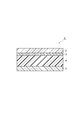
- FIG. 1 It is a schematic cross section showing one embodiment of a photosensitive element of this indication. It is a figure which shows typically an example of the manufacturing process of the printed wiring board by a semi-additive construction method.
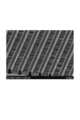
- 4 is a SEM photograph of a resist pattern obtained in Example 3.
- 4 is a SEM photograph of a resist pattern obtained in Comparative Example 1.
- (meth) acrylic acid means at least one of acrylic acid and methacrylic acid corresponding thereto.
- (meth) acrylate means at least one of acrylic acid and methacrylic acid corresponding thereto.
- process is not limited to an independent process, and even if it cannot be clearly distinguished from other processes, the term “process” is used as long as the intended action of the process is achieved. included.
- the numerical range indicated using “ ⁇ ” in this specification indicates a range including the numerical values described before and after “ ⁇ ” as the minimum value and the maximum value, respectively.
- the upper limit value or lower limit value of a numerical range of a certain step may be replaced with the upper limit value or lower limit value of the numerical range of another step.
- the upper limit value or the lower limit value of the numerical range may be replaced with the values shown in the examples.
- the term “layer” includes a structure formed in a part in addition to a structure formed in the entire surface when observed as a plan view.
- the photosensitive element 1 of the present embodiment includes a support film 2, an intermediate layer 3, and a photosensitive layer 4 in this order, and further includes other layers such as a protective layer 5. Good.
- a support film 2 As shown in FIG. 1, the photosensitive element 1 of the present embodiment includes a support film 2, an intermediate layer 3, and a photosensitive layer 4 in this order, and further includes other layers such as a protective layer 5. Good.
- a protective layer 5 Good.
- each layer in the photosensitive element according to the present embodiment will be described in detail.
- the thickness of the support film is 20 ⁇ m or more, and the number of particles having a diameter of 5 ⁇ m or more contained in the support film is 30 / mm 2 or less.
- shape trace transfer to the intermediate layer of particles such as a lubricant present in the support film can be suppressed and used for exposure. Since scattering (for example, irregular reflection) of actinic rays can be suppressed, an excellent patterning property can be obtained, and a resist pattern with few minute omissions can be formed.
- the transfer of the particle shape traces such as a lubricant to the intermediate layer allows the exposure process.
- Light scattering occurs, and minute omissions are likely to occur in the resist pattern after development.
- the influence of the light scattering becomes greater, and minute omissions are more likely to occur in the resist pattern after development.
- a photosensitive element When such a photosensitive element is used for the production of a printed wiring board, it causes the occurrence of open defects during etching and the occurrence of short-circuit defects during plating, thereby reducing the production yield of the printed wiring board.
- the thickness of the support film is 20 ⁇ m or more, but may be 25 ⁇ m or more, or 45 ⁇ m or more.
- the thickness of the support film may be 200 ⁇ m or less, or 100 ⁇ m or less. By making the thickness of the support film 200 ⁇ m or less, there is a tendency that economic benefits are easily obtained.
- the “thickness of the support film” means the length in the direction orthogonal to the surface direction of the support film, and the “particle shape trace” means “the shape trace derived from particles such as a lubricant”.
- the number of particles having a diameter of 5 ⁇ m or more contained in the support film is 30 particles / mm 2 or less. From the viewpoint of further preventing scattering of exposure light due to transfer of particle shape traces, the number of particles having a diameter of 5 ⁇ m or more is 25. Pieces / mm 2 or less, 20 pieces / mm 2 or less, 10 pieces / mm 2 or less, 5 pieces / mm 2 or less, or 1 piece / mm 2 or less. By reducing the number of particles having a diameter of 5 ⁇ m or more to 30 particles / mm 2 or less, a resist pattern formed by using the photosensitive element according to the present embodiment is less likely to have a minute drop, and a resist having a small amount of missing.
- a pattern can be formed. And when such a photosensitive element is used for the production of a printed wiring board, it is possible to suppress the occurrence of open defects during etching and the occurrence of short-circuit defects during plating, and suppress the reduction in the production yield of printed wiring boards. it can.
- the lower limit of the number of particles having a diameter of 5 ⁇ m or more contained in the support film is 0 / mm 2 .
- the particle having a diameter of 5 ⁇ m or more contained in the support film means a diameter of 5 ⁇ m or more when the particle is observed using a polarizing microscope (however, if the observed particle shape is not circular, its shape is circumscribed) Means a particle present on the surface of the support film.
- the particle is not particularly limited as long as it gives unevenness to the layer in contact with the support film.
- the lubricant is included to add slipperiness to the surface of the support film, and organically sprayed onto the support film intentionally.
- Particles or inorganic particles (hereinafter also referred to as “sprayed particles”), foreign matter, aggregates (for example, agglomerates of lubricants, agglomerates of spray particles, or gels of polymers, monomers as raw materials, and support film production)
- a catalyst to be used an agglomerate formed by agglomerating inorganic or organic fine particles contained when necessary), a lubricant generated when a lubricant layer (a layer containing a lubricant) is applied on a support film, and Including swelling with adhesive.
- the shape of the particles is not particularly limited, but may be a regular shape such as a spherical shape or an irregular shape.
- the material of the particles is not particularly limited, and may be an organic material or an inorganic material such as a metal. In order to reduce the number of particles having a diameter of 5 ⁇ m or more to 30 particles / mm 2 or less, among these particles, a particle having a small particle diameter or a particle having excellent dispersibility may be selectively used.
- the number of particles having a diameter of 5 ⁇ m or more can be measured using a polarizing microscope. More specifically, both surfaces of the support film are observed with a polarizing microscope, the number of particles having a diameter of 5 ⁇ m or more on both surfaces of the support film is integrated, and the obtained number of particles having a diameter of 5 ⁇ m or more contained in the support film. It is a number.
- the support film is transparent (that is, the haze is 5% or less)
- each of the one surface and the other surface of the support film is observed while focusing on the surface, and the number of particles having a diameter of 5 ⁇ m or more. Measure.
- the measurement area has a size of 1 mm square and is measured at least at 10 locations, and the average value is the number of particles having a diameter of 5 ⁇ m or more contained in the support film.
- the aggregate formed by aggregating primary particles having a diameter of 5 ⁇ m or more and primary particles having a diameter of less than 5 ⁇ m is counted as one.
- “aggregation” means a state in which particles (for example, primary particles) are in contact with each other or close to each other at 1 ⁇ m or less and form a larger aggregate as compared with each particle.
- the number of particles having a diameter of 2 ⁇ m or more and less than 5 ⁇ m included in the support film may be 1000 / mm 2 or less, 500 / mm 2 or less, or 10 / mm 2 or less.
- the lower limit of the number of particles is 0 / mm 2 .
- the number of particles having a diameter of 2 ⁇ m or more and less than 5 ⁇ m correlates with the number of particles having a diameter of 5 ⁇ m or more. If the number of particles having a diameter of 5 ⁇ m or more is small, the number of particles having a diameter of 2 ⁇ m or more and less than 5 ⁇ m also decreases.
- the number of particles having a diameter of less than 2 ⁇ m contained in the support film is not particularly limited. Even if many particles having a diameter of less than 2 ⁇ m are contained in the support film, the influence on light scattering is not great. The reason for this is that, in the exposure process, when the photosensitive layer is irradiated with light, the photocuring reaction of the photosensitive layer is not only the light irradiation part, but is slight, but the lateral direction (light irradiation direction) where light is not directly irradiated. To the vertical direction).
- NA numerical aperture
- the support film may have particles such as lubricant on the surface opposite to the surface in contact with the intermediate layer of the support film, or may have particles such as lubricant on the surface in contact with the intermediate layer of the support film.
- the number of intermediate layers in contact with the above diameter 5 ⁇ m in the plane particles of the support film, from the viewpoint of preventing the scattering of the exposure light beam by the transfer of the particle shape remains Furthermore, 10 pieces / mm 2 or less, 5 / mm 2 or less, Alternatively, it may be 1 piece / mm 2 or less.
- the lower limit of the number of particles is 0 / mm 2 . By setting it as such a range, there exists a tendency which makes it easy to form a resist pattern with few minute omissions.
- the lubricant layer may be formed on the support film using a known method such as roll coating, flow coating, spray coating, curtain flow coating, dip coating, slit die coating, or the like. it can.
- the support film having the lubricant or the lubricant layer may contain 1000 or more lubricants / mm 2 having a diameter of less than 1 ⁇ m in order to perform the function of the lubricant.
- the support film may have a layer (region) that does not have particles.
- the thickness of the layer having no particles may be 17 ⁇ m or more, 19 ⁇ m or more, or 21 ⁇ m or more.
- the thickness of the layer having no particles is 17 ⁇ m or more, there is a tendency that minute omissions generated in the resist pattern can be further suppressed.
- minute omissions generated in the resist pattern can be further suppressed.
- the “thickness of the layer not having particles” means the length of the region where particles are not present in the direction (thickness direction) orthogonal to the surface direction of the support film. It means the maximum value of the distance between the planes (straight lines in cross-sectional observation) perpendicular to the thickness direction that are in contact with the mutually facing sides of the two closest particles in the thickness direction. Further, when the layer having particles is present only on one side of the support film, the “thickness of the layer not having particles” is the surface of the support film opposite to the side on which the layer having particles is present; It means the distance between planes (straight lines in cross-sectional observation) perpendicular to the thickness direction of the particles closest to the surface that are in contact with the side facing the surface.
- grain can be measured by observing the cross section of a support film with a scanning electron microscope (SEM). Further, when observing with SEM, processing by a focused ion beam processing observation apparatus (FIB) may be performed. Further, the average surface depth of particles having a diameter of 5 ⁇ m or more contained in the support film may be 2 ⁇ m or less, 1 ⁇ m or less, or 0.5 ⁇ m or less.
- the average surface depth of particles having a diameter of 5 ⁇ m or more refers to an average value of the depth at which particles having a diameter of 5 ⁇ m or more are fitted into the support film when the cross section of the support film is observed with a scanning electron microscope.
- the thickness of the support film may be 20 ⁇ m or more, and the surface roughness Rz of the surface in contact with the intermediate layer of the support film may be 500 nm or less.
- the surface roughness Rz may be 300 nm or less, 100 nm or less, or 80 nm or less.
- the surface roughness Rz may be 1 nm or more, 5 nm or more, 15 nm or more, or 25 nm or more.
- surface roughness Rz says the value measured using the commercially available surface roughness shape measuring machine based on the method prescribed
- the haze of the support film is 0.01 to 5.0%, 0.01 to 2 It may be 0.0%, 0.01 to 1.5%, 0.01 to 1.0%, or 0.01 to 0.5%. If the haze is 0.01% or more, the support film itself tends to be easily produced, and if it is 5.0% or less, it tends to be easily obtained.
- “haze” means cloudiness.
- the haze in the present disclosure refers to a value measured using a commercially available haze meter (turbidimeter) in accordance with the method defined in JIS K 7105. The haze can be measured with a commercially available turbidimeter such as NDH-5000 (manufactured by Nippon Denshoku Industries Co., Ltd.).
- the material of the support film can be used without any particular limitation.
- examples thereof include polyesters such as polyethylene terephthalate (PET), polybutylene terephthalate (PBT), and polyethylene-2,6-naphthalate (PEN), and polyolefins such as polypropylene and polyethylene.
- PET polyethylene terephthalate
- PBT polybutylene terephthalate
- PEN polyethylene-2,6-naphthalate
- polyolefins such as polypropylene and polyethylene.
- the support film may be a single layer or a multilayer.
- a support film that can be used as a support film for the photosensitive element may be obtained from commercially available general industrial films. Specifically, for example, “QS series” (manufactured by Toray Industries, Inc.), “A4100” (manufactured by Toyobo Co., Ltd.), “KFX” (manufactured by Teijin DuPont Films Ltd.), etc., which are PET films.
- QS series manufactured by Toray Industries, Inc.
- A4100 manufactured by Toyobo Co., Ltd.
- KFX manufactured by Teijin DuPont Films Ltd.
- the photosensitive element of this embodiment includes an intermediate layer between the support film and the photosensitive layer. Thereby, even if it peels and exposes a support film, the deterioration of the resolution of the resist pattern formed can be suppressed. Further, from the viewpoint of further improving the gas barrier property, the adhesive force between the support film and the intermediate layer may be smaller than the adhesive force between the intermediate layer and the photosensitive layer. That is, it can be said that when the support film is peeled from the photosensitive element, unintentional peeling between the intermediate layer and the photosensitive layer is suppressed.
- the intermediate layer can also be said to be an oxygen shielding layer.
- the intermediate layer may have water solubility or may have solubility in a developer.
- middle layer is a layer formed using the resin composition for intermediate
- the resin contained in the resin composition for forming an intermediate layer has an oxygen transmission coefficient of 1 ⁇ 10 ⁇ 13 cm 3 (STP) cm / (cm 2 ⁇ s ⁇ Pa) or less from the viewpoint of workability and oxygen shielding properties. , 1 ⁇ 10 -14 cm 3 ( STP) cm / (cm 2 ⁇ s ⁇ Pa) or less, or, even 1 ⁇ 10 -15 cm 3 (STP ) cm / (cm 2 ⁇ s ⁇ Pa) or less Good.
- the resin composition for forming an intermediate layer may contain a water-soluble resin. By including the water-soluble resin, the solubility of the formed intermediate layer tends to be improved.
- the stability tends to be improved in order to keep the separation between the formed intermediate layer and the photosensitive layer easily for a long period.
- the water-soluble resin include polyvinyl alcohol and polyvinyl pyrrolidone.
- the intermediate layer forming resin composition may contain polyvinyl alcohol from the viewpoint that the oxygen permeability coefficient is low and the radical deactivation caused by the actinic rays used for exposure can be further suppressed.
- Polyvinyl alcohol can be obtained, for example, by saponifying polyvinyl acetate obtained by polymerizing vinyl acetate.
- the saponification degree of the polyvinyl alcohol used in the present embodiment may be 50 mol% or more, 70 mol% or more, or 80 mol% or more.
- the gas barrier property of the intermediate layer can be further improved, and the resolution of the resist pattern to be formed tends to be further improved.
- the “degree of saponification” in the present specification refers to a value measured in accordance with JIS K 6726 (1994) (Testing method for polyvinyl alcohol) defined by Japanese Industrial Standards.
- 100 mol% may be sufficient as the upper limit of this saponification degree.
- the average degree of polymerization of polyvinyl alcohol may be 300-3500, 300-2500, or 300-1000.
- the average polymerization degree of polyvinylpyrrolidone may be 10,000 to 100,000, or 10,000 to 50,000.
- As the polyvinyl alcohol two or more kinds of polyvinyl alcohols having different saponification degree, viscosity, polymerization degree, modified species and the like may be used in combination.
- the intermediate layer forming resin composition may include a resin having solubility in a developer.
- resin which has the solubility with respect to a developing solution (A) component used for the photosensitive resin composition mentioned later may be included, and (B) component may be included, for example.
- the resin composition for forming an intermediate layer can contain at least one solvent as necessary in order to improve the handleability of the resin composition or to adjust the viscosity and storage stability.
- the solvent include water and organic solvents.
- the organic solvent include methanol, acetone, toluene, or a mixed solvent thereof. From the viewpoint of improving the efficiency of drying when forming the intermediate layer, methanol may be included.
- the resin composition for forming an intermediate layer contains a water-soluble resin, water and methanol
- the methanol content is 1 to 100 parts by mass with respect to 100 parts by mass of water from the viewpoint of solubility in the water-soluble resin. It may be 10 to 80 parts by mass, or 20 to 60 parts by mass.
- the content of the water-soluble resin may be 1 to 50 parts by mass, or 10 to 30 parts by mass with respect to 100 parts by mass of water.
- the intermediate layer forming resin composition may contain known additives such as a surfactant, a plasticizer, and a leveling agent.
- a leveling agent examples include a silicone leveling agent, and examples of a commercially available silicone leveling agent include Polyflow KL-401 (manufactured by Kyoeisha Chemical Co., Ltd.).
- the content of the leveling agent is 0.01 to 2.0 with respect to 100 parts by mass of the intermediate layer-forming resin composition from the viewpoint of easy formation of the intermediate layer. It may be part by mass or 0.05 to 1.0 part by mass.
- a silicone surfactant or a fluorosurfactant can be contained from the viewpoint of improving the peelability from the support film.
- These surfactants can be used alone or in combination of two or more.
- the content of the surfactant is 0.01 to 1.0 part by mass with respect to 100 parts by mass of the resin composition for forming an intermediate layer from the viewpoint of easy formation of the intermediate layer. 0.05 to 0.5 parts by mass, or 0.1 to 0.3 parts by mass.
- a polyhydric alcohol compound can be included from the viewpoint of improving the ease of forming the intermediate layer.
- glycerins such as glycerin, diglycerin and triglycerin
- (poly) alkylene glycols such as ethylene glycol, diethylene glycol, triethylene glycol, tetraethylene glycol, polyethylene glycol, propylene glycol, dipropylene glycol and polypropylene glycol, and trimethylol Examples include propane.
- These plasticizers can be used alone or in combination of two or more.
- the thickness of the intermediate layer is not particularly limited, but may be 12 ⁇ m or less, 10 ⁇ m or less, or 8 ⁇ m or less from the viewpoint of developability. Further, the thickness of the intermediate layer may be 1.0 ⁇ m or more, 1.5 ⁇ m or more, or 2 ⁇ m or more from the viewpoint of ease of forming the intermediate layer and resolution.
- the intermediate layer in this embodiment may have photosensitivity, but the photosensitivity is lower than the photosensitivity of the photosensitive layer. Further, the intermediate layer may not have photosensitivity. When the intermediate layer does not have photosensitivity, the photosensitivity stability of the photosensitive layer tends to be further improved.
- Photosensitive means, for example, exposing the photosensitive layer, subjecting it to a heat treatment after exposure, and then developing the photosensitive layer using a developer for removing uncured portions of the photosensitive layer. In this case, a resist pattern can be formed.
- the photosensitive layer of this embodiment is a layer formed using the photosensitive resin composition mentioned later.
- the photosensitive resin composition can be used in accordance with a desired purpose as long as it is a resin composition whose properties change (for example, photocures) when irradiated with light. There may be.
- the photosensitive resin composition may contain (A) a binder polymer, (B) a photopolymerizable compound, and (C) a photopolymerization initiator. Moreover, you may contain (D) photosensitizer, (E) polymerization inhibitor, or another component as needed.
- each component used by the photosensitive resin composition of this embodiment is demonstrated in detail.
- the binder polymer (hereinafter also referred to as “component (A)”) can be produced, for example, by radical polymerization of a polymerizable monomer.
- the polymerizable monomer include polymerizable styrene derivatives substituted at the ⁇ -position or aromatic ring such as styrene, vinyl toluene and ⁇ -methylstyrene, acrylamide such as diacetone acrylamide, acrylonitrile, vinyl -Ethers of vinyl alcohol such as n-butyl ether, (meth) acrylic acid alkyl ester, (meth) acrylic acid benzyl ester such as benzyl methacrylate, (meth) acrylic acid tetrahydrofurfuryl ester, (meth) acrylic acid dimethylaminoethyl Ester, (meth) acrylic acid diethylaminoethyl ester, (meth) acrylic acid glycidy
- a (meth) acrylic acid alkyl ester may be included from the viewpoint of improving plasticity.
- examples of the (meth) acrylic acid alkyl ester include compounds represented by the following general formula (II) and compounds in which the alkyl group of these compounds is substituted with a hydroxyl group, an epoxy group, a halogen group or the like.
- R 6 represents a hydrogen atom or a methyl group
- R 7 represents an alkyl group having 1 to 12 carbon atoms.
- alkyl group having 1 to 12 carbon atoms represented by R 7 include methyl group, ethyl group, propyl group, butyl group, pentyl group, hexyl group, heptyl group, octyl group, nonyl group, decyl group, undecyl group. Groups, dodecyl groups and structural isomers of these groups.
- Examples of the (meth) acrylic acid alkyl ester represented by the general formula (II) include (meth) acrylic acid methyl ester, (meth) acrylic acid ethyl ester, (meth) acrylic acid propyl ester, and (meth) acrylic.
- Acid butyl ester (meth) acrylic acid pentyl ester, (meth) acrylic acid hexyl ester, (meth) acrylic acid heptyl ester, (meth) acrylic acid octyl ester, (meth) acrylic acid 2-ethylhexyl ester, (meth) acrylic Examples include acid nonyl ester, (meth) acrylic acid decyl ester, (meth) acrylic acid undecyl ester, (meth) acrylic acid dodecyl ester, and the like. These can be used individually by 1 type or in combination of 2 or more types.
- the component (A) may contain a carboxyl group from the viewpoint of alkali developability.
- the component (A) containing a carboxyl group can be produced, for example, by radical polymerization of a polymerizable monomer having a carboxyl group and another polymerizable monomer.
- the polymerizable monomer having a carboxyl group may be (meth) acrylic acid or methacrylic acid.
- the acid value of the component (A) containing a carboxyl group may be 50 to 250 mgKOH / g.
- Carboxyl group content (mixing ratio of polymerizable monomer having a carboxyl group with respect to the total amount of polymerizable monomers used in the binder polymer) is a viewpoint that improves alkali developability and alkali resistance in a balanced manner. From 12 to 50% by mass, from 12 to 40% by mass, from 15 to 35% by mass, or from 15 to 30% by mass. When the carboxyl group content is 12% by mass or more, alkali developability tends to be improved, and when it is 50% by mass or less, alkali resistance tends to be excellent.
- styrene or a styrene derivative may be used as a polymerizable monomer from the viewpoint of adhesion and chemical resistance.
- the content thereof (the blending ratio of styrene or styrene derivative with respect to the total amount of the polymerizable monomer used in component (A)) is determined by adhesion and chemical resistance. From the standpoint of further improving, it may be 10 to 60% by mass or 15 to 50% by mass. When the content is 10% by mass or more, the adhesion tends to be improved. When the content is 60% by mass or less, it is possible to suppress an increase in the size of the peeling piece during development, and it is possible to suppress the lengthening of the time required for peeling. is there.
- (meth) acrylic acid benzyl ester may be used as a polymerizable monomer from the viewpoint of resolution and aspect ratio.
- the content of the structural unit derived from (meth) acrylic acid benzyl ester in the component (A) may be 15 to 50% by mass from the viewpoint of further improving the resolution and aspect ratio.
- binder polymers can be used singly or in combination of two or more.
- the component (A) when two or more types are used in combination for example, two or more types of binder polymers composed of different polymerizable monomers, two or more types of binder polymers having different weight average molecular weights, and different dispersions are used. 2 or more types of binder polymers.
- a component can be manufactured by a normal method. Specifically, for example, it can be produced by radical polymerization of (meth) acrylic acid alkyl ester, (meth) acrylic acid, styrene and the like.
- the weight average molecular weight of the component (A) is 20,000 to 300,000, 40,000 to 150,000, 40,000 to 120,000, or from the viewpoint of improving the mechanical strength and alkali developability in a balanced manner. 50,000 to 80,000.
- the weight average molecular weight of the component (A) is 20,000 or more, the developer resistance tends to be excellent, and when it is 300,000 or less, the development time tends to be suppressed.
- the weight average molecular weight in this specification is a value measured by a gel permeation chromatography method (GPC) and converted by a calibration curve created using standard polystyrene.
- the content of the component (A) is 30 to 80 parts by mass, 40 to 75 parts by mass, or 50 to 70 parts by mass with respect to 100 parts by mass of the solid content of the component (A) and the component (B) described later. Part. When the content of the component (A) is within this range, the coating property of the photosensitive resin composition and the strength of the photocured portion are improved.
- the photosensitive resin composition according to the present embodiment may include (B) a photopolymerizable compound (hereinafter also referred to as “component (B)”).
- component (B) can be used without particular limitation as long as it is a photopolymerizable compound or a photocrosslinkable compound.
- a compound having at least one ethylenically unsaturated bond in the molecule is used. it can.
- component (B) examples include photopolymerizable compounds having an ethylenically unsaturated bond described in International Publication No. 2015/177947. These can be used individually by 1 type or in combination of 2 or more types.
- the component (B) may contain a bisphenol type (meth) acrylate compound from the viewpoint of improving the resolution, adhesion, and resist skirt generation in a well-balanced manner.
- the bisphenol type (meth) acrylate compound may be a compound represented by the following general formula (III).
- R 1 , R 2 , R 3 and R 4 each independently represent a hydrogen atom or a methyl group.
- X and Y each independently represent an ethylene group or a propylene group, and XO and YO each independently represent an oxyethylene group (hereinafter sometimes referred to as “EO group”) or an oxypropylene group (hereinafter referred to as “PO”). May be referred to as a “group”).
- EO group oxyethylene group
- PO oxypropylene group
- p 1 , p 2 , q 1 and q 2 each independently represent a numerical value of 0 to 40. However, both p 1 + q 1 and p 2 + q 2 are 1 or more.
- p 1 + p 2 is 1 to 40
- q 1 + q 2 is 0 to 20
- p 1 + p 2 is 0 to 20
- q 1 + q 2 is 1 to 40. Since p 1 , p 2 , q 1 and q 2 indicate the number of structural units of the EO group or PO group, a single molecule indicates an integer value, and an aggregate of a plurality of types of molecules indicates an average rational number. Show. Note that the EO group and the PO group may be continuously present in blocks or randomly.
- the content of the compound is based on the total solid content of the component (A) and the component (B) from the viewpoint of improving chemical resistance. It may be 1 to 50% by mass, or 3 to 40% by mass.
- the content of the bisphenol type (meth) acrylate compound is 30 to 99% by mass, 50 to 97% by mass, or 50% to 97% by mass with respect to the total solid content of the component (B), from the viewpoint of further improving chemical resistance. It may be 60 to 95% by mass.
- a compound obtained by reacting a polyhydric alcohol with an ⁇ , ⁇ -unsaturated carboxylic acid may be contained.
- polyalkylene glycol di (meth) acrylate having both EO group and PO group in the molecule dipentaerythritol (meth) acrylate having EO group, and the like can be used.
- Examples of the commercially available compound as dipentaerythritol (meth) acrylate having an EO group include “DPEA-12” manufactured by Nippon Kayaku Co., Ltd.
- the content of the dipentaerythritol (meth) acrylate having an EO group is 1 to 10% by mass or 1.5% from the viewpoint of better resolution with respect to the total solid content of the component (A) and the component (B). It may be up to 5% by weight.
- polyalkylene glycol di (meth) acrylate having both EO group and PO group for example, poly having EO group: 6 (average value) and PO group: 12 (average value) And alkylene glycol dimethacrylate (“FA-023M”, “FA-024M” manufactured by Hitachi Chemical Co., Ltd.).
- the EO group and the PO group may be present continuously in blocks or randomly.
- the PO group may be either an oxy-n-propylene group or an oxyisopropylene group.
- the secondary carbon of the propylene group may be bonded to an oxygen atom, or the primary carbon may be bonded to an oxygen atom.
- the content of the component (B) may be 20 to 70 parts by mass, 25 to 60 parts by mass, or 30 to 50 parts by mass with respect to 100 parts by mass of the total solid content of the components (A) and (B). Good.
- the content of the component (B) is within this range, in addition to the resolution of the photosensitive resin composition, the adhesion and the suppression of resist skirt generation, the photosensitivity and the coating property are also improved.
- the photosensitive resin composition according to the present embodiment may contain at least one (C) photopolymerization initiator (hereinafter also referred to as “component (C)”).
- component (C) is not particularly limited as long as it can polymerize the component (B), and can be appropriately selected from commonly used photopolymerization initiators.
- component (C) examples include 2-benzyl-2-dimethylamino-1- (4-morpholinophenyl) -butanone-1,2-methyl-1- [4- (methylthio) phenyl] -2-morpholino- Aromatic ketones such as propanone-1, quinones such as alkyl anthraquinones, benzoin ether compounds such as benzoin alkyl ether, benzoin compounds such as benzoin and alkylbenzoin, benzyl derivatives such as benzyldimethyl ketal, 2- (o-chlorophenyl)- 2,4,5-triarylimidazole dimer such as 4,5-diphenylimidazole dimer, 2- (o-fluorophenyl) -4,5-diphenylimidazole dimer, 9-phenylacridine, 1, Acridine derivatives such as 7- (9,9′-acridinyl) heptane Can be mentioned. These can be used individually by 1 type or in
- 2,4,5-triarylimidazole dimer may be contained from the viewpoint of improving resolution.
- Examples of the 2,4,5-triarylimidazole dimer include 2- (o-chlorophenyl) -4,5-diphenylimidazole dimer, 2- (o-chlorophenyl) -4,5-bis- And (m-methoxyphenyl) imidazole dimer and 2- (p-methoxyphenyl) -4,5-diphenylimidazole dimer.
- 2- (o-chlorophenyl) -4,5-diphenylimidazole dimer may be contained from the viewpoint of improving the light sensitivity stability.
- 2,4,5-triarylimidazole dimer examples include 2,2′-bis (2-chlorophenyl) -4,4 ′, 5,5′-tetraphenylbiimidazole, Commercially available as Tsuchiya Chemical Co., Ltd.).
- Component (C) contains at least one 2,4,5-triarylimidazole dimer from the viewpoint of further improving the photosensitivity and adhesion, and further suppressing the light absorption of component (C).
- 2- (2-chlorophenyl) -4,5-diphenylimidazole dimer may be included.
- the 2,4,5-triarylimidazole dimer may have a symmetric structure or an asymmetric structure.
- the content of the component (C) is 0.01 to 30 parts by weight, 0.1 to 10 parts by weight, 1 to 7 parts by weight with respect to 100 parts by weight of the total solid content of the components (A) and (B). It may be 1 to 6 parts by mass, 1 to 5 parts by mass, or 2 to 5 parts by mass.
- the content of the component (C) is 0.01 parts by mass or more, the photosensitivity, resolution, and adhesion tend to be improved, and when it is 30 parts by mass or less, the resist shape tends to be excellent.
- the photosensitive resin composition according to the present embodiment may include (D) a photosensitizer (hereinafter also referred to as “component (D)”). By containing the component (D), the absorption wavelength of actinic rays used for exposure can be effectively used.
- component (D) a photosensitizer
- component (D) examples include pyrazolines, dialkylaminobenzophenones, anthracene, coumarins, xanthones, oxazoles, benzoxazoles, thiazoles, benzothiazoles, triazoles, stilbenes, triazines, thiophenes , Naphthalimides and triarylamines. These can be used individually by 1 type or in combination of 2 or more types. From the standpoint that the absorption wavelength of actinic rays used for exposure can be used more effectively, component (D) may contain pyrazolines, anthracenes, or dialkylaminobenzophenones, and in particular, dialkylaminobenzophenones. But you can. Examples of commercially available compounds as dialkylaminobenzophenones include “EAB” manufactured by Hodogaya Chemical Co., Ltd.
- the content is 1.0 mass part or less, 0.5 mass part or less, 0.1 mass part or less with respect to 100 mass parts of solid content total of (A) component and (B) component. It may be 15 parts by mass or less, 0.12 parts by mass or less, or 0.10 parts by mass or less.
- content of the component (D) is 1.0 part by mass or less with respect to 100 parts by mass of the total solid content of the component (A) and the component (B)
- the deterioration of the resist shape and resist bottom generation is suppressed. There is a tendency that the resolution can be improved.
- content of (D) component is 0.01 mass part or more with respect to 100 mass parts of solid content total amount of (A) component and (B) component from a viewpoint from which high photosensitivity and high resolution are easy to be obtained. It may be.
- the photosensitive resin composition according to the present embodiment may include (E) a polymerization inhibitor (hereinafter also referred to as “component (E)”).
- component (E) a polymerization inhibitor
- the component (E) may contain a compound represented by the following general formula (I) from the viewpoint of further improving the resolution.
- R 5 represents a halogen atom, a hydrogen atom, an alkyl group having 1 to 20 carbon atoms, a cycloalkyl group having 3 to 10 carbon atoms, an amino group, an aryl group, a mercapto group, or 1 to 10 carbon atoms.
- An alkyl mercapto group, a carboxyl alkyl group having 1 to 10 carbon atoms, an alkoxy group having 1 to 20 carbon atoms or a heterocyclic group, wherein m and n are an integer of 2 or more, and n is R is an integer of 0 or more and is an integer selected such that m + n 6.
- R 5 may be the same or different.
- the aryl group may be substituted with an alkyl group having 1 to 20 carbon atoms.
- R 5 may be a hydrogen atom or an alkyl group having 1 to 20 carbon atoms from the viewpoint of further improving the compatibility with the component (A).
- the alkyl group having 1 to 20 carbon atoms represented by R 5 may be an alkyl group having 1 to 4 carbon atoms.
- m may be 2 or 3, or 2 from the viewpoint of further improving the resolution.
- the compound represented by the general formula (I) may be alkylcatechol from the viewpoint of further improving the resolution.
- the content of the component (E) is 0.03 to 0.3 parts by mass, 0.03 to 0.2 parts by mass, 0.03 to 0.2 parts by mass with respect to 100 parts by mass of the total solid content of the components (A) and (B). It may be from 05 to 0.15 parts by mass, or from 0.05 to 0.1 parts by mass.
- the exposure time can be shortened, which tends to contribute to the improvement of mass production efficiency.
- content of (E) component 0.03 mass part or more the photoreaction of a photocuring part can fully advance, resist swellability is suppressed by the reaction rate improvement, and resolution is improved. There is a tendency to be better.
- the content of the component (E) is 0.05 to 0.4 parts by mass, 0.05 to 0.2 parts by mass, or 0.05 to 100 parts by mass of the solid content of the component (A). It may be up to 0.1 parts by mass.
- content of (E) component is 0.05 mass part or more with respect to (A) component, there exists a tendency which can improve the thermal stability of the photosensitive resin composition, and is 0.4 mass part or less. When it is, there exists a tendency which can suppress yellowing of the photosensitive resin composition.
- an additive described in International Publication No. 2015/177947 is added to 100 parts by mass of the total solid content of the component (A) and the component (B). Each can be contained in an amount of 0.01 to 20 parts by mass.
- additives can be used alone or in combination of two or more.
- the photosensitive resin composition according to the present embodiment is at least one organic solvent as necessary in order to improve the handleability of the photosensitive resin composition or to adjust the viscosity and storage stability.
- the organic solvent normally can be especially used without a restriction
- a protective layer can be laminated on the surface of the photosensitive layer opposite to the surface in contact with the intermediate layer.
- a protective layer for example, a polymer film such as polyethylene or polypropylene may be used.
- the polymer film similar to the support film mentioned above may be used, and a different polymer film may be used.
- a water-soluble resin containing polyvinyl alcohol is gradually added to water heated to 70 to 90 ° C. so as to have a solid content of 10 to 20% by mass, and stirred uniformly for about 1 hour. It is made to melt
- the “solid content” refers to a non-volatile content excluding volatile substances such as water and organic solvents of the resin composition. That is, it refers to components other than solvents such as water and organic solvents that remain without volatilization in the drying step, and include liquid, syrup-like and wax-like components at room temperature around 25 ° C.
- the resin composition for forming an intermediate layer is applied on a support film and dried to form an intermediate layer.
- the density of particles, such as a lubricant differs in both surfaces of a support film, you may form an intermediate
- Application of the intermediate layer forming resin composition onto the support film can be performed by a known method such as roll coating, comma coating, gravure coating, air knife coating, die coating, bar coating, spray coating, or the like.
- the drying of the applied resin composition for forming an intermediate layer is not particularly limited as long as at least a part of a solvent such as water can be removed, but may be dried at 70 to 150 ° C. for 5 to 30 minutes. After drying, the amount of residual solvent in the intermediate layer may be 2% by mass or less from the viewpoint of preventing solvent diffusion in the subsequent step.
- the photosensitive resin composition is applied onto the intermediate layer of the support film on which the intermediate layer is formed in the same manner as the application of the resin composition for forming the intermediate layer and dried to form a photosensitive layer on the intermediate layer. May be.
- a protective layer on the photosensitive layer thus formed, a photosensitive element comprising a support film, an intermediate layer, a photosensitive layer, and a protective layer in this order can be produced.
- the support film, the intermediate layer, the photosensitive layer, and the protective layer are bonded to each other by attaching the intermediate layer formed on the support film and the protective layer formed on the protective layer. You may obtain the photosensitive element provided in order.
- the photosensitive element according to this embodiment is manufactured by such bonding, workability tends to be improved.
- the thickness of the photosensitive layer in the photosensitive element can be appropriately selected depending on the application, but it may be 1 to 200 ⁇ m, 5 to 100 ⁇ m, or 10 to 50 ⁇ m after drying.
- the thickness of the photosensitive layer is 1 ⁇ m or more, industrial coating becomes easy and productivity tends to be improved.
- the thickness of the photosensitive layer is 200 ⁇ m or less, the photosensitivity is high and the photocurability at the bottom of the resist is excellent, so that a resist pattern having excellent resolution and aspect ratio tends to be formed.
- the melt viscosity at 110 ° C. of the photosensitive layer in the photosensitive element can be appropriately selected depending on the type of the substrate in contact with the photosensitive layer, but after drying, at 110 ° C., 50 to 10,000 Pa ⁇ s, 100 to 5000 Pa ⁇ s, Alternatively, it may be 200 to 1000 Pa ⁇ s.
- the melt viscosity at 110 ° C. is 50 Pa ⁇ s or more, wrinkles and voids are not generated in the lamination step, and the productivity tends to be improved.
- the melt viscosity at 110 ° C. is 10000 Pa ⁇ s or less, the adhesion to the base is improved in the laminating step, and the adhesion failure tends to be reduced.
- the photosensitive element according to the present embodiment can be suitably used for, for example, a resist pattern forming method and a printed wiring board manufacturing method described later.
- the resist pattern forming method includes (i) a step of arranging the photosensitive layer, the intermediate layer, and the support film in this order on a substrate using the photosensitive element (hereinafter, “ (I) photosensitive layer and intermediate layer forming step), and (ii) removing the support film and exposing the photosensitive layer with active light through the intermediate layer (hereinafter referred to as “(ii) exposure”). And (iii) a step of removing the uncured portion of the photosensitive layer and the intermediate layer from the substrate (hereinafter also referred to as “(iii) development step”). Other steps may be included.
- a resist pattern is a photocured material pattern of the photosensitive resin composition, and can also be called a relief pattern.
- the resist pattern in the present embodiment may be used as a resist or may be used for other applications such as a protective film.
- the photosensitive layer and intermediate layer forming step In the photosensitive layer and intermediate layer forming step, the photosensitive layer and the intermediate layer are formed on the substrate using the photosensitive element.
- substrate for circuit formation provided with the insulating layer and the conductor layer formed on the insulating layer, or die pads (base material for lead frames), such as an alloy base material, etc. Used.
- the protective layer is removed and then the photosensitive layer of the photosensitive element is heated.
- the photosensitive layer and the intermediate layer can be formed on the substrate.
- the photosensitive layer and intermediate layer forming step When the photosensitive layer and intermediate layer forming step is performed using the photosensitive element, it may be performed under reduced pressure from the viewpoint of adhesion and followability. Heating at the time of pressure bonding may be performed at a temperature of 70 to 130 ° C., and pressure bonding may be performed at a pressure of 0.1 to 1.0 MPa (1 to 10 kgf / cm 2 ), but these conditions are necessary. It can be selected as appropriate. If the photosensitive layer of the photosensitive element is heated to 70 to 130 ° C., it is not necessary to pre-heat the substrate in advance, but in order to further improve the adhesion and followability, the substrate is pre-heated. You can also.
- the support film is removed, and the photosensitive layer is exposed with actinic rays through the intermediate layer.
- the exposed part irradiated with actinic rays may be photocured to form a photocured part (latent image), and the unexposed part not irradiated with actinic rays is photocured, A photocured portion may be formed.
- the support film present on the photosensitive layer is peeled off and then exposed.
- a known exposure method can be applied.
- a method (projection exposure method) of irradiating in an image form through a lens using an actinic ray on which an image of a photomask is projected may be mentioned.
- a projection exposure method may be used from the viewpoint of further suppressing the occurrence of minute omission of the resist pattern. That is, the photosensitive element according to the present embodiment is applied to the projection exposure method.
- the projection exposure method can also be said to be an exposure method using an actinic ray having an attenuated energy amount.
- the light source of the actinic ray is not particularly limited as long as it is a known light source that is usually used.
- a light source that effectively emits ultraviolet rays such as a solid-state laser such as a semiconductor laser, a semiconductor laser such as a gallium nitride blue-violet laser, or the like is used. Further, a light source that effectively emits visible light, such as a photographic flood bulb or a solar lamp, may be used.
- a light source capable of emitting i-line monochromatic light with an exposure wavelength of 365 nm a light source capable of emitting h-line monochromatic light with an exposure wavelength of 405 nm, or an ihg mixed line
- a light source capable of emitting an actinic ray having an exposure wavelength may be used, and a light source capable of emitting i-line monochromatic light having an exposure wavelength of 365 nm may be used.
- Examples of the light source capable of emitting i-line monochromatic light having an exposure wavelength of 365 nm include an ultrahigh pressure mercury lamp.
- the uncured portion and the intermediate layer of the photosensitive layer are removed from the substrate.
- a resist pattern including a photocured portion obtained by photocuring the photosensitive layer is formed on the substrate.
- the intermediate layer is water-soluble, the intermediate layer may be removed by washing with water, and then the uncured portion other than the photocured portion may be removed with a developer, and the intermediate layer is dissolved in the developer. If it has the property, the intermediate layer may be removed together with the uncured portion other than the photocured portion by a developer.
- Examples of the development method include wet development.
- wet development can be performed by a known wet development method using a developer corresponding to the photosensitive resin composition.
- the wet development method include a dipping method, a paddle method, a high-pressure spray method, a method using brushing, slapping, scrubbing, rocking immersion, and the like. From the viewpoint of improving resolution, a high-pressure spray method is used. Is the most suitable.
- These wet development methods may be developed singly or in combination of two or more methods.
- the developer is appropriately selected according to the configuration of the photosensitive resin composition.
- alkaline aqueous solution and organic solvent developer are mentioned.
- an alkaline aqueous solution may be used as the developer.
- the base of the alkaline aqueous solution include alkali hydroxide such as lithium, sodium or potassium hydroxide, alkali carbonate such as lithium, sodium, potassium or ammonium carbonate or bicarbonate, potassium phosphate, sodium phosphate Alkali metal phosphates such as sodium pyrophosphate and potassium pyrophosphate, sodium borate, sodium metasilicate, tetramethylammonium hydroxide, ethanolamine, ethylenediamine, diethylenetriamine, 2-amino-2- Hydroxymethyl-1,3-propanediol, 1,3-diamino-2-propanol and morpholine are used.
- Examples of the alkaline aqueous solution used for development include a dilute solution of 0.1 to 5% by mass of sodium carbonate, a dilute solution of 0.1 to 5% by mass of potassium carbonate, a dilute solution of 0.1 to 5% by mass of sodium hydroxide, A dilute solution of 1 to 5% by mass sodium tetraborate or the like can be used.
- the pH of the alkaline aqueous solution used for development may be in the range of 9 to 11, and the temperature of the alkaline aqueous solution can be adjusted according to the developability of the photosensitive layer.
- a surface active agent, an antifoaming agent, a small amount of an organic solvent for accelerating development may be mixed.
- Examples of the organic solvent used in the alkaline aqueous solution include 3-acetone alcohol, acetone, ethyl acetate, alkoxyethanol having an alkoxy group having 1 to 4 carbon atoms, ethyl alcohol, isopropyl alcohol, butyl alcohol, diethylene glycol monomethyl ether, Examples include diethylene glycol monoethyl ether and diethylene glycol monobutyl ether.
- organic solvent used in the organic solvent developer examples include 1,1,1-trichloroethane, N-methylpyrrolidone, N, N-dimethylformamide, cyclohexanone, methyl isobutyl ketone and ⁇ -butyrolactone. From the viewpoint of preventing ignition, these organic solvents may be added with water so as to be in the range of 1 to 20% by mass to obtain an organic solvent developer.
- the laminate of this embodiment may include a substrate, a photosensitive layer, and an intermediate layer in this order, and may further include a support film on the surface of the intermediate layer opposite to the photosensitive layer.
- the diameter of the surface of the intermediate layer opposite to the photosensitive layer side is 3 ⁇ m or more.
- the number of dents is 30 pieces / mm 2 or less.
- the number of recesses having a diameter of 3 ⁇ m or more is 25 pieces / mm 2 or less, 20 pieces / mm 2 or less, 10 pieces / mm 2 or less, 5 pieces / mm 2 or less, or 1 piece / mm 2 or less. May be.
- the lower limit of the number of such dents is 0 / mm 2 .
- the number of dents can be measured using a scanning electron microscope.
- the number of recesses having a diameter of 1.2 ⁇ m or more and less than 3 ⁇ m is 1000 / mm 2 or less, 500 / mm 2 or less, or 10 / mm 2. Although the following may be sufficient, the lower limit of the number of such dents is 0 piece / mm ⁇ 2 >.
- the depth of the recess may be 5 ⁇ m or less.
- the laminate may not have a support film on the surface on the side opposite to the photosensitive layer of the intermediate layer, that is, the layer on the side opposite to the photosensitive layer of the intermediate layer. The surface may be exposed.
- the number of recesses having a diameter of 3 ⁇ m or more on the surface opposite to the photosensitive layer of the intermediate layer can be reduced by reducing the number of particles contained in the support film, particularly the number of particles having a diameter of 5 ⁇ m or more.
- the number of recesses having a diameter of 1.2 ⁇ m or more and less than 3 ⁇ m on the surface of the intermediate layer opposite to the photosensitive layer reduces the number of particles contained in the support film, particularly the number of particles having a diameter of 2 ⁇ m or more and less than 5 ⁇ m. Can be reduced.
- the number of recesses having a diameter of 3 ⁇ m or more can be measured by observing with a scanning electron microscope (for example, SU-1500 (manufactured by Hitachi, Ltd.)). Observation can be performed at any 10 locations.
- the measurement area has a size of 1 mm square, measurements are made at 10 arbitrary points, and the average value is the number of recesses having a diameter of 3 ⁇ m or more in the intermediate layer.
- a scanning electron microscope for example, SU-1500 (manufactured by Hitachi, Ltd.)
- Observation can be performed at any 10 locations.
- the measurement area has a size of 1 mm square, measurements are made at 10 arbitrary points, and the average value is the number of recesses having a diameter of 3 ⁇ m or more in the intermediate layer.
- the substrate is not particularly limited, but the same substrates as those listed in the resist pattern forming method may be used.
- the surface roughness Rz of the substrate may be 100 nm or less, 80 nm or less, or 50 nm or less from the viewpoint of improving resolution.
- the surface roughness Rz of the substrate is not particularly limited, but may be 1 nm or more.
- the laminate of this embodiment may be manufactured by pressing the photosensitive element onto the substrate so that the photosensitive layer of the photosensitive element is in close contact with the substrate.
- the laminate of this embodiment includes a step of exposing the photosensitive layer with actinic rays through an intermediate layer in the laminate, and a step of removing the uncured portion of the photosensitive layer and the intermediate layer from the substrate. It can be used in a method for forming a resist pattern. Thereby, it is possible to form a resist pattern with few minute omissions.
- the method for manufacturing a printed wiring board according to the present embodiment includes a step of forming a conductor pattern by etching or plating a substrate on which a resist pattern has been formed by the above-described resist pattern forming method. Other steps such as a removal step may be included.
- the method for producing a printed wiring board according to the present embodiment can be suitably used for forming a conductor pattern by using the method for forming a resist pattern using the photosensitive element or the laminate. The application to the method of forming is more preferable.
- the conductor pattern can be said to be a circuit.
- the conductor layer of the substrate not covered with the resist is removed by etching to form a conductor pattern.
- Etching method is appropriately selected according to the conductor layer to be removed.
- the etching solution include a cupric chloride solution, a ferric chloride solution, an alkaline etching solution, a hydrogen peroxide-based etching solution, etc., and a ferric chloride solution is used from the point that the etch factor is good. Also good.
- the plating process copper or solder is plated on the conductor layer of the substrate not covered with the resist, using the resist pattern formed on the substrate provided with the conductor layer as a mask. After the plating treatment, the resist is removed by removing a resist pattern, which will be described later, and the conductor layer covered with this resist is etched to form a conductor pattern.
- the plating treatment method may be electrolytic plating treatment or electroless plating treatment, but may be electroless plating treatment.
- electroless plating treatment include copper plating such as copper sulfate plating and copper pyrophosphate plating, solder plating such as high-throw solder plating, nickel plating such as watt bath (nickel sulfate-nickel chloride) plating and nickel sulfamate plating, Gold plating such as hard gold plating and soft gold plating can be used.
- the resist pattern on the substrate is removed.
- the resist pattern can be removed by, for example, a stronger alkaline aqueous solution than the alkaline aqueous solution used in the development step.
- a strong alkaline aqueous solution for example, a 1 to 10% by mass sodium hydroxide aqueous solution, a 1 to 10% by mass potassium hydroxide aqueous solution and the like are used. Among these, a 1 to 5% by mass aqueous sodium hydroxide solution or an aqueous potassium hydroxide solution may be used.
- Examples of the resist pattern removal method include an immersion method and a spray method, and these may be used alone or in combination.
- a desired printed wiring board can be manufactured by further etching the conductor layer covered with the resist by etching to form a conductor pattern.
- the etching method at this time is appropriately selected according to the conductor layer to be removed. For example, the above-described etching solution can be applied.
- the printed wiring board manufacturing method according to the present embodiment can be applied not only to a single-layer printed wiring board but also to a multilayer printed wiring board, and also to a printed wiring board having a small-diameter through hole. Is possible.
- the method for manufacturing a printed wiring board according to the present embodiment can be suitably used for manufacturing a high-density package substrate, particularly for manufacturing a wiring board by a semi-additive construction method.
- An example of the manufacturing process of the wiring board by the semi-additive construction method is shown in FIG.
- FIG. 2A a substrate (circuit forming substrate) in which the conductor layer 40 is formed on the insulating layer 50 is prepared.
- the conductor layer 40 is, for example, a copper layer.
- FIG. 2B the photosensitive layer 30 and the intermediate layer 20 are formed on the conductor layer 40 of the substrate by the photosensitive layer and intermediate layer forming step.
- FIG. 2C the photocuring portion is formed in the photosensitive layer 30 by irradiating the photosensitive layer 30 with the actinic ray 80 on which the image of the photomask is projected on the photosensitive layer 30 through the intermediate layer 20 in the exposure process.
- FIG. 2A a substrate (circuit forming substrate) in which the conductor layer 40 is formed on the insulating layer 50 is prepared.
- the conductor layer 40 is, for example, a copper layer.
- FIG. 2B the photosensitive layer 30 and the intermediate layer 20 are formed on the conductor layer 40 of the substrate by the photosensitive layer and intermediate layer forming step.
- FIG. 2C the photocur
- the resist pattern 32 which is a photocured portion, is formed on the substrate by removing the region (including the intermediate layer) other than the photocured portion formed by the exposure step from the substrate by the developing process.
- the plating layer 60 is formed on the conductor layer 40 of the board
- FIG. 2F after the resist pattern 32 which is a photocuring portion is peeled off with a strong alkaline aqueous solution, the conductor layer 40 masked by the resist pattern 32 is removed by a flash etching process, and the plating after the etching process is performed.
- a conductor pattern 70 including the layer 62 and the conductor layer 42 after the etching process is formed.
- the conductor layer 40 and the plating layer 60 may be made of the same material or different materials. When the conductor layer 40 and the plating layer 60 are the same material, the conductor layer 40 and the plating layer 60 may be integrated.
- the resist pattern 32 may be formed by using both a mask exposure method and a direct drawing exposure method.
- binder polymers (A-1) shown in Tables 2 and 3 below were synthesized according to Synthesis Example 1.
- a solution b 1.2 g of azobisisobutyronitrile was dissolved in 100 g of a mixed solution (mass ratio 3: 2) of 60 g of methyl cellosolve and 40 g of toluene to prepare a solution b.
- a mixed solution of methyl cellosolve and toluene having a mass ratio of 3: 2 (hereinafter also referred to as “mixed solution x”). 400g was added, it stirred while blowing nitrogen gas, and it heated to 80 degreeC.
- the solution a was added dropwise to the mixed solution x in the flask over a period of 4 hours at a constant dropping rate, followed by stirring at 80 ° C. for 2 hours.
- the solution b was dropped into the solution in the flask at a constant dropping rate over 10 minutes, and then the solution in the flask was stirred at 80 ° C. for 3 hours.
- the temperature of the solution in the flask was raised to 90 ° C. over 30 minutes, kept at 90 ° C. for 2 hours, and then cooled to room temperature to obtain a solution of binder polymer (A-1).
- a solution of the binder polymer (A-1) was prepared by adding the mixed solution x so that the nonvolatile component (solid content) was 50% by mass.
- the weight average molecular weight of the binder polymer (A-1) was 50,000, and the acid value was 163 mgKOH / g.
- the acid value was measured by a neutralization titration method. Specifically, 30 g of acetone was added to 1 g of the binder polymer solution, and further uniformly dissolved, and then an appropriate amount of an indicator, phenolphthalein, was added to the binder polymer solution to obtain a 0.1 N aqueous KOH solution. It measured by performing titration using.
- the weight average molecular weight was measured by gel permeation chromatography (GPC), and was derived by conversion using a standard polystyrene calibration curve. The GPC conditions are shown below.
- the photosensitive resin composition was obtained by mixing each component shown in the following Table 3 by the quantity (unit: mass part) shown in the same table.
- all compounding quantities other than the organic solvent of Table 3 are compounding quantities in solid content.
- Photopolymerization initiator * 10 B-CIM (Hodogaya Chemical Co., Ltd.) 2,2'-bis (2-chlorophenyl) -4,4 ', 5,5'-tetraphenylbiimidazole
- the number of particles having a diameter of 5 ⁇ m or more was determined by observing both surfaces of the support film with a polarizing microscope, measuring the number of particles having a diameter of 5 ⁇ m or more, and integrating these numbers. In this observation, each of the one surface and the other surface of the support film was observed while focusing on the surface. In addition, the number n of the measurement area (size of 1 mm square) of the support film was 10, and the average value was obtained.
- the intermediate layer 1 or 2 was formed on the surface of the PET film with the less lubricant using the intermediate layer forming resin composition 1 or 2.
- each component of the intermediate layer forming resin composition 1 other than water is slowly added to water at room temperature. Until heated. After reaching 90 ° C., the mixture was stirred for 1 hour and cooled to room temperature. Next, the intermediate layer forming resin composition 1 is applied on the PET film (support film) so that the thickness is uniform, and is dried for 10 minutes in a hot air convection dryer at 95 ° C. An intermediate layer 1 having a thickness of 5 ⁇ m was formed.
- the intermediate layer forming resin composition 2 (acrylic resin composition) is applied on the support film so that the thickness is uniform. And it dried for 10 minutes with a 100 degreeC hot-air convection type dryer, and formed the intermediate
- the photosensitive resin composition is applied on the intermediate layer of the support film so that the thickness is uniform, and is dried for 10 minutes with a hot air convection dryer at 100 ° C., and the thickness after drying is 10 ⁇ m.
- a photosensitive layer was formed.
- the photosensitive layer formed using the photosensitive resin composition 1 is also referred to as a photosensitive layer 1
- the photosensitive layer formed using the photosensitive resin composition 2 is also referred to as a photosensitive layer 2.
- a polyethylene film (protective layer) (manufactured by Tamapoly Co., Ltd., “NF-15”) is laminated on the photosensitive layer, and a PET film (support film), an intermediate layer, a photosensitive layer, a protective layer, Obtained a photosensitive element laminated in this order.
- the intermediate layer 1 is formed on the QS63 (support film) using the intermediate layer forming resin composition 1, and then the photosensitive resin composition is formed on the intermediate layer 1. It means that the photosensitive layer 1 was formed using the product 1.
- ⁇ Production of laminate> After the copper surface of a copper-clad laminate (substrate, manufactured by Hitachi Chemical Co., Ltd., “MCL-E-67”), which is a glass epoxy material in which copper foil with a thickness of 12 ⁇ m is laminated on both sides, is acid-treated and washed with water, then air Dried in a stream.
- the copper-clad laminate was heated to 80 ° C., and while peeling off the protective layer, the photosensitive elements were respectively pressed onto the copper-clad laminate so that the photosensitive layer was in contact with the copper surface.
- the pressure bonding was performed using a 110 ° C. heat roll at a roll speed of 1.0 m / min at a pressure of 0.40 MPa.
- the support film is peeled from the laminate, and a recess of a diameter of 3 ⁇ m or more (hereinafter also referred to as “intermediate layer recess”) on the surface of the intermediate layer opposite to the photosensitive layer side is referred to as a scanning electron microscope SU-1500 ( (Manufactured by Hitachi, Ltd.).
- the number n of measurement regions (size of 1 mm square) of the intermediate layer was 10, and the average value was obtained and evaluated according to the following criteria.
- the results are shown in Tables 4 to 6 below.
- A The number of recesses having a diameter of 3 ⁇ m or more is less than 5.
- B The number of recesses having a diameter of 3 ⁇ m or more is 5 or more and 30 or less.
- C The number of depressions having a diameter of 3 ⁇ m or more exceeds 30.
- ⁇ Photosensitivity measurement test> The support film is peeled off from the test piece, a Hitachi 41-step tablet is placed on the intermediate layer of the test piece, and a projection exposure machine having a high-pressure mercury lamp with a wavelength of 365 nm (“UX-2240SM-” manufactured by USHIO INC.) XJ01 ”, NA: 0.063) to adjust the irradiation amount to obtain a predetermined irradiation energy amount (exposure amount) at which the number of steps of the resist pattern after development (resist curing step number) becomes seven steps.
- the photosensitive layer was exposed through the intermediate layer.
- the photosensitive layer was spray-developed using a 1% by mass aqueous sodium carbonate solution at 30 ° C. in a time twice as short as the shortest development time, and the unexposed area was removed.
- the intermediate layer was water-soluble (in the case of the intermediate layer 1)
- the photosensitive layer was developed after washing with water.
- the intermediate layer was soluble in the developer (in the case of the intermediate layer 2)
- the intermediate layer was removed together with the unexposed portion by development.
- the shortest development time was calculated
- the photosensitive layer was exposed through the intermediate layer with an irradiation energy amount of 7 steps. After the exposure, the same development processing as in the photosensitivity measurement test was performed.
- a photosensitive element a laminate, a method for forming a resist pattern, and a method for manufacturing a printed wiring board, which can form a resist pattern with few microscopic omissions.
Landscapes
- Engineering & Computer Science (AREA)
- Physics & Mathematics (AREA)
- General Physics & Mathematics (AREA)
- Microelectronics & Electronic Packaging (AREA)
- Manufacturing & Machinery (AREA)
- Chemical & Material Sciences (AREA)
- Spectroscopy & Molecular Physics (AREA)
- Polymers & Plastics (AREA)
- Health & Medical Sciences (AREA)
- Chemical Kinetics & Catalysis (AREA)
- Medicinal Chemistry (AREA)
- Organic Chemistry (AREA)
- Structural Engineering (AREA)
- Architecture (AREA)
- Materials For Photolithography (AREA)
- Manufacturing Of Printed Circuit Boards (AREA)
- Manufacturing Of Printed Wiring (AREA)
Abstract
Description
本実施形態の感光性エレメント1は、図1に示すように、支持フィルム2と、中間層3と、感光層4とをこの順で備え、保護層5等のその他の層を更に備えてもよい。以下、本実施形態に係る感光性エレメントにおける各層について詳述する。
本実施形態の感光性エレメントにおいて、上記支持フィルムの厚みは20μm以上であり、該支持フィルムに含まれる直径5μm以上の粒子の数は30個/mm2以下である。支持フィルムの厚み及び支持フィルムに含まれる粒子の数が上記範囲内にあることで、支持フィルムに存在する滑剤等の粒子の中間層への形状跡転写を抑制することができ、露光に用いられる活性光線の散乱(例えば、乱反射)を抑制できるため、優れたパターニング性が得られ、微小な抜けが少ないレジストパターンを形成することができる。一方、従来の感光性エレメントでは、解像性を向上する観点で露光工程の前に支持フィルムを剥離した場合であっても、中間層への滑剤等の粒子形状跡の転写により、露光工程で光散乱を起こし、現像後のレジストパターンに微小な抜けが生じ易くなる。また、高解像度露光機を使用した場合、その光散乱による影響がより大きくなり、現像後のレジストパターンに微小な抜けがより生じ易くなる。このような感光性エレメントをプリント配線板の製造に使用すると、エッチング時のオープン不良発生及びめっき時のショート不良発生の一因になり、プリント配線板の製造歩留りが低下する。
本実施形態の感光性エレメントは、支持フィルムと感光層との間に中間層を備える。これによって、支持フィルムを剥離して露光したとしても、形成されるレジストパターンの解像性の悪化を抑制することができる。また、ガスバリア性を更に向上する観点から、支持フィルムと中間層との接着力は、中間層と感光層との接着力より小さくてもよい。すなわち、感光性エレメントから支持フィルムを剥離した場合、中間層と感光層との意図せぬ剥離が抑制されている、ともいえる。また、中間層は、酸素遮蔽層ともいえる。また、中間層は、水溶性を有していてもよく、現像液に対する溶解性を有していてもよい。中間層は、後述する中間層形成用樹脂組成物を用いて形成される層である。
中間層形成用樹脂組成物に含まれる樹脂としては、作業性及び酸素遮蔽性の観点で、酸素透過係数が、1×10-13cm3(STP)cm/(cm2・s・Pa)以下、1×10-14cm3(STP)cm/(cm2・s・Pa)以下、又は、1×10-15cm3(STP)cm/(cm2・s・Pa)以下であってもよい。中間層形成用樹脂組成物は、水溶性樹脂を含んでもよい。水溶性樹脂を含むことによって、形成される中間層の溶解性が向上する傾向がある。また、形成される中間層と感光層との層分離を長い期間保ち続け易くするため、安定性が向上する傾向がある。水溶性樹脂としては、例えば、ポリビニルアルコール、ポリビニルピロリドン等が挙げられる。酸素透過係数が低く、露光に用いられる活性光線によって発生したラジカルの失活をより抑制できる観点から、中間層形成用樹脂組成物は、ポリビニルアルコールを含んでもよい。ポリビニルアルコールは、例えば、酢酸ビニルを重合して得られるポリ酢酸ビニルをけん化して得ることができる。本実施形態で用いられるポリビニルアルコールのけん化度は、50モル%以上、70モル%以上、又は、80モル%以上であってもよい。けん化度が50モル%以上であるポリビニルアルコールを用いることにより、中間層のガスバリア性をより向上させることができ、形成されるレジストパターンの解像性をより向上させることができる傾向がある。なお、本明細書における「けん化度」は、日本工業規格で規定するJIS K 6726(1994)(ポリビニルアルコールの試験方法)に準拠して測定される値をいう。また、かかるけん化度の上限値は、100モル%であってもよい。
本実施形態の感光層は、後述する感光性樹脂組成物を用いて形成される層である。感光性樹脂組成物は、光照射されることによって性質が変わる(例えば、光硬化する)樹脂組成物であれば、所望の目的に合わせて用いることができ、ネガ型であってもポジ型であってもよい。感光性樹脂組成物は、(A)バインダーポリマー、(B)光重合性化合物及び(C)光重合開始剤を含有してもよい。また、必要に応じて、(D)光増感剤、(E)重合禁止剤又はその他の成分を含有してもよい。以下、本実施形態の感光性樹脂組成物で用いられる各成分についてより詳細に説明する。
(A)バインダーポリマー(以下、「(A)成分」ともいう)は、例えば、重合性単量体をラジカル重合させることにより製造することができる。上記重合性単量体としては、例えば、スチレン、ビニルトルエン及びα-メチルスチレン等のα-位又は芳香族環において置換されている重合可能なスチレン誘導体、ジアセトンアクリルアミド等のアクリルアミド、アクリロニトリル、ビニル-n-ブチルエーテル等のビニルアルコールのエーテル類、(メタ)アクリル酸アルキルエステル、ベンジルメタクリレート等の(メタ)アクリル酸ベンジルエステル、(メタ)アクリル酸テトラヒドロフルフリルエステル、(メタ)アクリル酸ジメチルアミノエチルエステル、(メタ)アクリル酸ジエチルアミノエチルエステル、(メタ)アクリル酸グリシジルエステル、2,2,2-トリフルオロエチル(メタ)アクリレート、2,2,3,3-テトラフルオロプロピル(メタ)アクリレート、(メタ)アクリル酸、α-ブロモアクリル酸、α-クロルアクリル酸、β-フリル(メタ)アクリル酸、β-スチリル(メタ)アクリル酸、マレイン酸、マレイン酸無水物、マレイン酸モノメチル、マレイン酸モノエチル、マレイン酸モノイソプロピル等のマレイン酸モノエステル、フマール酸、ケイ皮酸、α-シアノケイ皮酸、イタコン酸、クロトン酸及びプロピオール酸が挙げられる。これらは1種を単独で又は2種以上を組み合わせて用いることができる。
H2C=C(R6)-COOR7 (II)
本実施形態に係る感光性樹脂組成物は、(B)光重合性化合物(以下、「(B)成分」ともいう)を含んでもよい。(B)成分は、光重合可能な化合物、光架橋可能な化合物であれば、特に制限なく用いることができるが、例えば、分子内に少なくとも1つのエチレン性不飽和結合を有する化合物を用いることができる。

本実施形態に係る感光性樹脂組成物は、(C)光重合開始剤(以下、「(C)成分」ともいう)を少なくとも1種含有してもよい。(C)成分は、(B)成分を重合させることができる成分であれば、特に制限は無く、通常用いられる光重合開始剤から適宜選択することができる。
本実施形態に係る感光性樹脂組成物は、(D)光増感剤(以下、「(D)成分」ともいう)を含んでもよい。(D)成分を含有することにより、露光に用いる活性光線の吸収波長を有効に利用することができる。
本実施形態に係る感光性樹脂組成物は、(E)重合禁止剤(以下、「(E)成分」ともいう)を含んでもよい。(E)成分を含有することにより、感光性樹脂組成物を光硬化させるために必要な露光量を、投影露光機で露光するのに最適な露光量に調整することができる傾向がある。

本実施形態に係る感光性樹脂組成物には、必要に応じて、国際公開第2015/177947に記載の添加剤を、(A)成分及び(B)成分の固形分総量100質量部に対して各々0.01~20質量部含有することができる。これらの添加剤は1種を単独で又は2種以上を組み合わせて用いることができる。
本実施形態の感光性エレメントは、感光層の中間層と接する面とは反対側の面に保護層を積層することもできる。保護層としては、例えば、ポリエチレン、ポリプロピレン等の重合体フィルムなどを用いてもよい。また、上述する支持フィルムと同様の重合体フィルムを用いてもよく、異なる重合体フィルムを用いてもよい。
まず、例えば、ポリビニルアルコールを含む水溶性樹脂を、固形分含有量が10~20質量%となるように、70~90℃に加温した水に徐々に加えて1時間程度撹拌して均一に溶解させて、ポリビニルアルコールを含む中間層形成用樹脂組成物を得る。なお、本明細書において、「固形分」とは、樹脂組成物の水、有機溶剤等の揮発する物質を除いた不揮発分を指す。すなわち、乾燥工程で揮発せずに残る、水、有機溶剤等の溶剤以外の成分を指し、25℃付近の室温で液状、水飴状及びワックス状の成分も含む。
本実施形態に係るレジストパターンの形成方法は、(i)上記感光性エレメントを用いて、基板上に、上記感光層と上記中間層と上記支持フィルムとをこの順で配置する工程(以下、「(i)感光層及び中間層形成工程」ともいう)と、(ii)上記支持フィルムを除去し、上記中間層を介して上記感光層を活性光線によって露光する工程(以下、「(ii)露光工程」ともいう)と、(iii)上記感光層の未硬化部及び上記中間層を上記基板上から除去する工程(以下、「(iii)現像工程」ともいう)と、を備え、必要に応じてその他の工程を含んでもよい。なお、レジストパターンとは、感光性樹脂組成物の光硬化物パターンともいえ、レリーフパターンともいえる。また、目的に応じて、本実施形態におけるレジストパターンは、レジストとして使用してもよいし、保護膜等の他の用途に使用してもよい。
感光層及び中間層形成工程においては、基板上に上記感光性エレメントを用いて感光層及び中間層を形成する。上記基板としては、特に制限されないが、通常、絶縁層と絶縁層上に形成された導体層とを備えた回路形成用基板、又は、合金基材等のダイパッド(リードフレーム用基材)などが用いられる。
露光工程においては、支持フィルムを除去し、中間層を介して感光層を活性光線によって露光する。これにより、活性光線が照射された露光部が光硬化して、光硬化部(潜像)が形成されていてもよく、また、活性光線が照射されていない未露光部が光硬化して、光硬化部が形成されていてもよい。上記感光性エレメントを用いて感光層及び中間層を形成した場合には、感光層上に存在する支持フィルムを剥離した後、露光する。中間層を介して感光層を露光することにより、解像性が向上し、レジストパターンの微小な抜けをより抑制することができる。
現像工程においては、上記感光層の未硬化部及び中間層を基板上から除去する。現像工程により、上記感光層が光硬化した光硬化部からなるレジストパターンが基板上に形成される。中間層が水溶性である場合には、水洗して中間層を除去してから、上記光硬化部以外の未硬化部を現像液により除去してもよく、中間層が現像液に対して溶解性を有する場合には、上記光硬化部以外の未硬化部と共に中間層を現像液により除去してもよい。現像方法には、ウェット現像が挙げられる。
本実施形態に係るレジストパターンの形成方法では、現像工程において未硬化部を除去した後、必要に応じて60~250℃での加熱又は0.2~10J/cm2の露光量での露光を行うことによりレジストパターンを更に硬化する工程を含んでもよい。
本実施形態の積層体は、基板と、感光層と、中間層とをこの順で備え、上記中間層の感光層側とは反対側の面に支持フィルムを更に備えてもよい。また、本実施形態の積層体において、中間層の感光層側とは反対側の面における直径(ただし、凹みの形状が円形でない場合には、その形状の外接円の直径を意味する)3μm以上の凹みの数は、30個/mm2以下である。また、当該直径3μm以上の凹みの数は、25個/mm2以下、20個/mm2以下、10個/mm2以下、5個/mm2以下、又は、1個/mm2以下であってもよい。かかる凹みの数の下限値は、0個/mm2である。なお、凹みの数は、走査型電子顕微鏡を用いて測定することができる。直径3μm以上の凹みの数を30個/mm2以下にすることで、当該積層体を用いて形成されるレジストパターンに微小な抜けが生じ難くなり、微小な抜けが少ないレジストパターンを形成することができる。そして、このような積層体をプリント配線板の製造に使用すると、エッチング時のオープン不良発生及びめっき時のショート不良発生を抑制でき、プリント配線板の製造歩留りが低下することを抑制できる。また、より微小な抜けが少ないレジストパターンを形成できる観点から、直径1.2μm以上3μm未満の凹みの数は、1000個/mm2以下、500個/mm2以下、又は、10個/mm2以下であってもよいが、かかる凹みの数の下限値は、0個/mm2である。また、同様の観点から、凹みの深さは、5μm以下であってもよい。また、同様の観点から、前記積層体において、中間層の感光層とは反対側の面に、支持フィルムを有していなくてもよく、すなわち積層体において中間層の感光層とは反対側の面が露出していてもよい。
本実施形態に係るプリント配線板の製造方法は、上記レジストパターンの形成方法によりレジストパターンが形成された基板をエッチング処理又はめっき処理して導体パターンを形成する工程を含み、必要に応じてレジストパターン除去工程等のその他の工程を含んでもよい。本実施形態に係るプリント配線板の製造方法は、上記感光性エレメント又は積層体によるレジストパターンの形成方法を使用することで、導体パターンの形成に好適に使用できるが、中でも、めっき処理により導体パターンを形成する方法への応用がより好適である。なお、導体パターンは、回路ともいえる。
重合性単量体としてメタクリル酸125g、メタクリル酸メチル25g、ベンジルメタクリレート125g及びスチレン225gを、アゾビスイソブチロニトリル1.5gと混合して、溶液aを調製した。
ポンプ:日立 L-6000型(株式会社日立製作所製)
カラム:以下の計3本(カラム仕様:10.7mmφ×300mm、いずれも日立化成株式会社製)
Gelpack GL-R420
Gelpack GL-R430
Gelpack GL-R440
溶離液:テトラヒドロフラン
試料濃度:固形分が50質量%のバインダーポリマーを120mg採取し、5mLのテトラヒドロフランに溶解して試料を調製した。
測定温度:25℃
流量:2.05mL/分
検出器:日立 L-3300型RI(株式会社日立製作所製)
次に、下記表1及び表2に示す各成分を同表に示す量(単位:質量部)で混合することにより、中間層形成用樹脂組成物1及び2を得た。なお、表1及び表2中の溶剤及び有機溶剤以外の配合量は、いずれも固形分での配合量である。

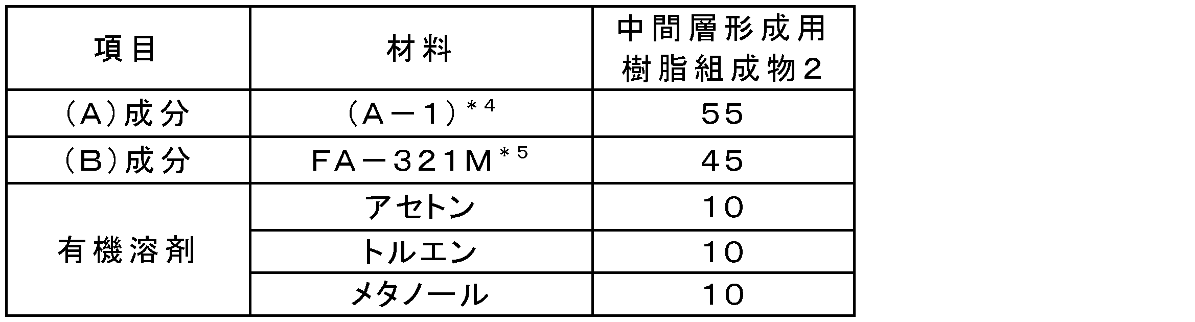
次に、下記表3に示す各成分を同表に示す量(単位:質量部)で混合することにより、感光性樹脂組成物を得た。なお、表3中の有機溶剤以外の配合量は、いずれも固形分での配合量である。
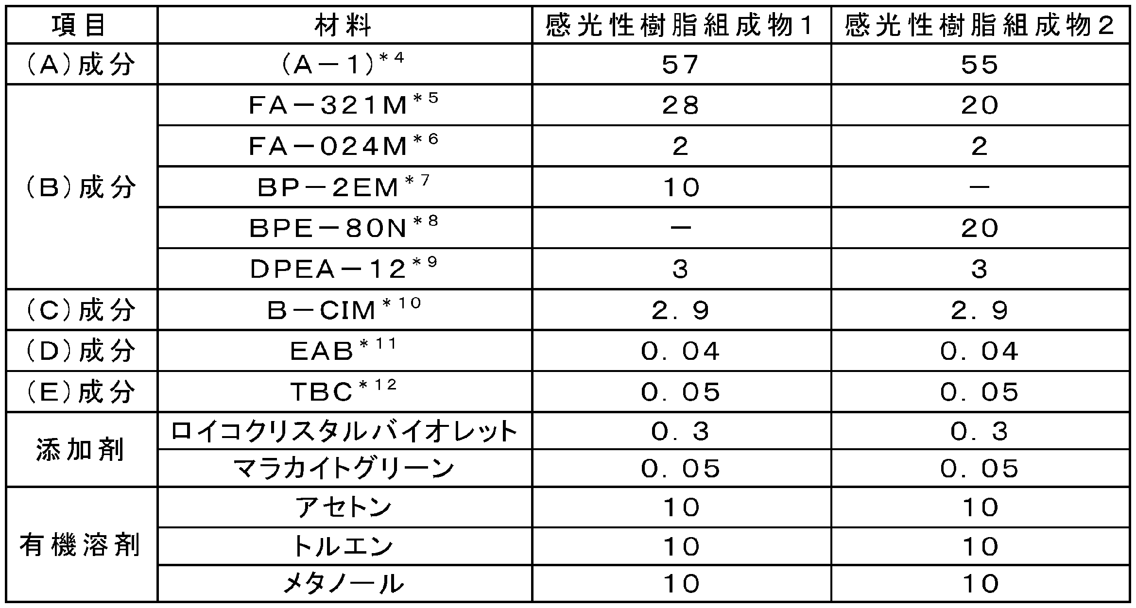
*1:ポリビニルアルコール PVA-205(株式会社クラレ製、けん化度=80モル%)
*2:ポリビニルピロリドン K-30(株式会社日本触媒製)
*3:ポリフロー KL-401(共栄社化学株式会社製)
*4:(A-1)(合成例1で得られたバインダーポリマー(A-1))
メタクリル酸/メタクリル酸メチル/ベンジルメタクリレート/スチレン=25/5/25/45(質量比)、重量平均分子量=50,000、固形分=50質量%、メチルセロソルブ/トルエン=3/2(質量比)溶液
*5:FA-321M(日立化成株式会社製)
2,2-ビス(4-(メタクリロキシペンタエトキシ)フェニル)プロパン
*6:FA-024M(日立化成株式会社製)
EOPO変性ジメタクリレート
*7:BP-2EM(共栄社化学株式会社製)
2,2-ビス(4-(メタクリロキシポリエトキシ)フェニル)プロパン
*8:BPE-80N(新中村化学工業株式会社製)
2,2-ビス(4-(メタクリロキシポリエトキシ)フェニル)プロパン
*9:DPEA-12(日本化薬株式会社製)
エチレンオキサイド変性ジペンタエリスリトールヘキサアクリレート
*10:B-CIM(保土谷化学工業株式会社製)
2,2’-ビス(2-クロロフェニル)-4,4’,5,5’-テトラフェニルビイミダゾール
*11:EAB(保土谷化学工業株式会社製)
4,4’-ビス(ジエチルアミノ)ベンゾフェノン
*12:TBC(DIC株式会社製)
4-tert-ブチルカテコール
<感光性エレメントの作製>
感光性エレメントの支持フィルムとして、下記表4~表6に示したPETフィルムを用意した。各PETフィルムに含まれる直径5μm以上の粒子の数を測定した結果を下記表4~表6に示す。また、PETフィルムはいずれも透明である。
PETフィルムの両面で粒子(滑剤)の密度が異なる場合には、PETフィルムの滑剤が少ない面に、中間層形成用樹脂組成物1又は2を用いて中間層1又は2を形成した。
次に、支持フィルムの中間層上に、厚みが均一になるように感光性樹脂組成物を塗布して、100℃の熱風対流式乾燥機で10分間乾燥し、乾燥後の厚みが10μmである感光層を形成した。以下、感光性樹脂組成物1を用いて形成された感光層を感光層1、感光性樹脂組成物2を用いて形成された感光層を感光層2ともいう。
厚み12μmの銅箔を両面に積層したガラスエポキシ材である銅張積層板(基板、日立化成株式会社製、「MCL-E-67」)の銅表面を、酸処理して水洗した後、空気流で乾燥した。銅張積層板を80℃に加温し、保護層を剥がしながら、感光層が銅表面に接するように、上記感光性エレメントをそれぞれ銅張積層板に圧着した。圧着は、110℃のヒートロールを用いて、0.40MPaの圧力で1.0m/分のロール速度で行った。こうして、基板、感光層、中間層及び支持フィルムの順に積層された積層体を得た。これらの積層体は、以下に示す試験における試験片として用いた。ラミネータとして、HLM-3000(大成ラミネーター株式会社製)を用いた。
上記積層体から支持フィルムを剥離し、中間層の感光層側とは反対側の面における、直径3μm以上の凹み(以下、「中間層凹み」ともいう)について、走査型電子顕微鏡SU-1500(株式会社日立製作所製)を用いて観察した。中間層の測定領域(1mm角の大きさ)数nは10とし、その平均値を求め、以下の基準で評価した。結果を下記表4~表6に示す。
A:直径3μm以上の凹みの数が5個未満。
B:直径3μm以上の凹みの数が5個以上30個以下。
C:直径3μm以上の凹みの数が30個を超える。
試験片から支持フィルムを剥離し、試験片の中間層上に、日立41段ステップタブレットを載置し、波長365nmの高圧水銀灯ランプを有する投影露光機(ウシオ電機株式会社製、「UX-2240SM-XJ01」、NA:0.063)を用いて、照射量を調整して現像後のレジストパターンのステップ段数(レジスト硬化段数)が7段となる所定の照射エネルギー量(露光量)を求めるために、中間層を介して感光層を露光した。
試験片から支持フィルムを剥離し、試験片の中間層上に、解像度評価用パターンとしてライン幅/スペース幅がz/z(z=2~20(1μm間隔で変化))(単位:μm)の配線パターンを有するガラスマスクを置いて、波長365nmの高圧水銀灯ランプを有する投影露光機(ウシオ電機株式会社製、「UX-2240SM-XJ01」)を用いて、日立41段ステップタブレットの現像後の残存ステップ段数が7段となる照射エネルギー量で、中間層を介して感光層を露光した。露光後、上記光感度測定試験と同様の現像処理を行った。現像処理後、光学顕微鏡を用いてレジストパターンを観察した。現像処理によって未露光部がきれいに除去されたライン部分(露光部)間のスペース幅のうち、最も小さい値(単位:μm)を解像度評価の指標とした。なお、この数値が小さいほど、解像度が良好であることを意味する。結果を下記表4~表6に示す。
上記解像度測定試験で得られたレジストパターンのうち、ライン幅が10μm(ライン幅と直交する長さが1mm)であるレジストパターン15本について、走査型電子顕微鏡SU-1500(株式会社日立製作所製)を用いて観察し、以下の基準で評価した。結果を下記表4~表6に示す。なお、実施例3で得られたレジストパターンのSEM写真は図3に示し、比較例1で得られたレジストパターンのSEM写真は図4に示す。
A:形成されたレジストパターンに直径が3μm以上の微小な抜けが5個未満。
B:形成されたレジストパターンに直径が3μm以上の微小な抜けが5個以上20個未満。
C:形成されたレジストパターンに直径が3μm以上の微小な抜けが20個以上。
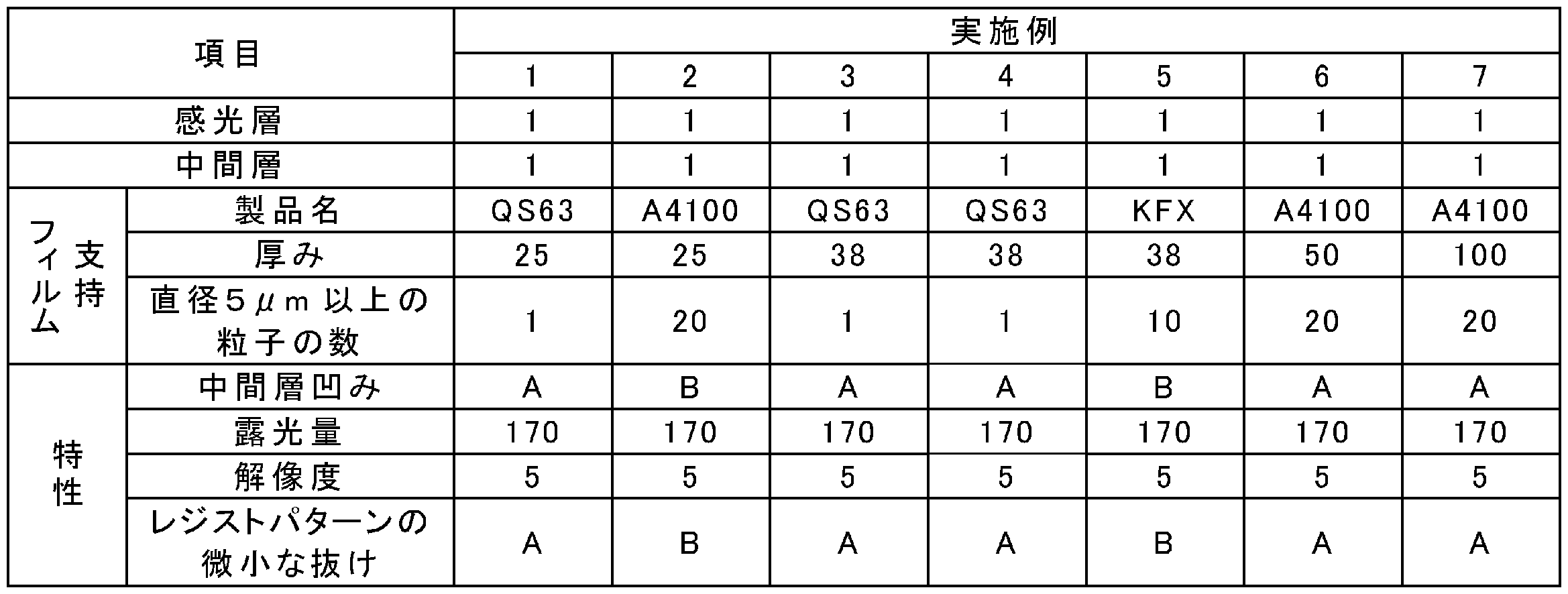
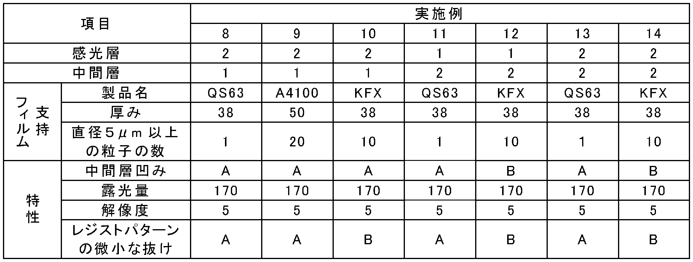
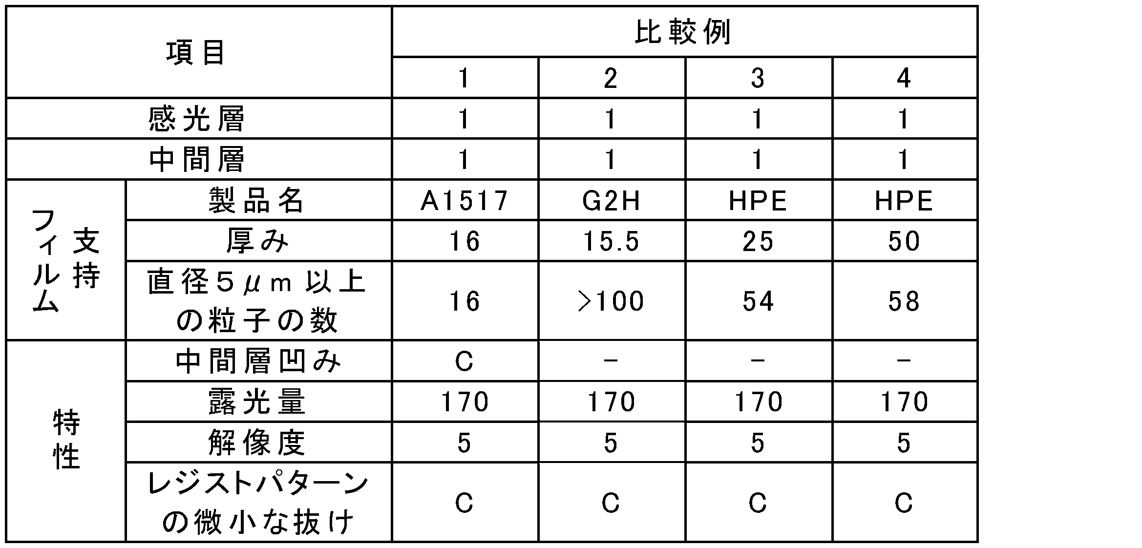
QS63:一方の面に滑剤層を有し、もう一方の面に滑剤層を有するが、含まれる滑剤の数が極めて少ない3層構造の二軸配向PETフィルム(東レ株式会社製、中間層と接する面における直径5μm以上の粒子の数(以下、単に、「中間層面の粒子数」という):1個/mm2以下、中間層と接する面における表面粗さRz:66nm)
A1517:滑剤層を一方の面に有する2層構造の二軸配向PETフィルム(東洋紡績株式会社製、中間層面の粒子数:10個/mm2以下、中間層と接する面における表面粗さRz:35nm)
A4100:滑剤層を一方の面に有する2層構造の二軸配向PETフィルム(東洋紡績株式会社製、中間層面の粒子数:10個/mm2以下、中間層と接する面における表面粗さRz:35nm)
G2H:滑剤を含有する単層構造(滑剤練り込みタイプ)の二軸配向PETフィルム(帝人デュポンフィルム株式会社製、中間層面の粒子数:10個/mm2を超える;中間層と接する面における表面粗さRz:920nm)
HPE:滑剤層を表裏に有する3層構造の二軸配向PETフィルム(帝人デュポンフィルム株式会社製、中間層面の粒子数:10個/mm2を超える;中間層と接する面における表面粗さRz:700nm)
KFX:滑剤層を一方の面に有する2層構造の二軸配向PETフィルム(帝人デュポンフィルム株式会社製、中間層面の粒子数:10個/mm2以下、中間層と接する面における表面粗さRz:50nm)
Claims (9)
- 支持フィルムと、中間層と、感光層とをこの順で備える感光性エレメントであって、前記支持フィルムの厚みが20μm以上であり、該支持フィルムに含まれる直径5μm以上の粒子の数が30個/mm2以下である、感光性エレメント。
- 前記支持フィルムの中間層と接する面における直径5μm以上の粒子の数が、10個/mm2以下である、請求項1に記載の感光性エレメント。
- 前記中間層が、ポリビニルアルコールを含む、請求項1又は2に記載の感光性エレメント。
- 前記支持フィルムが、ポリエステルフィルムである、請求項1~3のいずれか一項に記載の感光性エレメント。
- 請求項1~4のいずれか一項に記載の感光性エレメントを用いて、基板上に、前記感光層と前記中間層と前記支持フィルムとをこの順で配置する工程と、
前記支持フィルムを除去し、前記中間層を介して前記感光層を活性光線によって露光する工程と、
前記感光層の未硬化部及び前記中間層を前記基板上から除去する工程と、を備える、レジストパターンの形成方法。 - 前記露光を、レンズの開口数が0.05以上である高解像度露光機を用いて行う、請求項5に記載のレジストパターンの形成方法。
- 基板と、感光層と、中間層とをこの順で備え、前記中間層の前記感光層側とは反対側の面において、直径3μm以上の凹みの数が30個/mm2以下である、積層体。
- 請求項7に記載の積層体における前記中間層を介して、前記感光層を活性光線によって露光する工程と、
前記感光層の未硬化部及び前記中間層を前記基板上から除去する工程と、を含む、レジストパターンの形成方法。 - 請求項5、6又は8に記載のレジストパターンの形成方法によりレジストパターンが形成された基板をエッチング処理又はめっき処理して導体パターンを形成する工程を含む、プリント配線板の製造方法。
Priority Applications (6)
| Application Number | Priority Date | Filing Date | Title |
|---|---|---|---|
| CN202410174840.3A CN117835533A (zh) | 2015-07-08 | 2016-07-07 | 感光性元件、层叠体及其制造方法、抗蚀剂图案的形成方法和印刷配线板的制造方法 |
| MYPI2018700082A MY189073A (en) | 2015-07-08 | 2016-07-07 | Photosensitive element, laminated body, method for forming resist pattern, and method for producing printed circuit board |
| JP2017527500A JP6870611B2 (ja) | 2015-07-08 | 2016-07-07 | 感光性エレメント、積層体、レジストパターンの形成方法及びプリント配線板の製造方法 |
| CN201680039640.0A CN107850839A (zh) | 2015-07-08 | 2016-07-07 | 感光性元件、层叠体、抗蚀剂图案的形成方法和印刷配线板的制造方法 |
| KR1020237041794A KR102654084B1 (ko) | 2015-07-08 | 2016-07-07 | 감광성 엘리먼트, 적층체, 레지스터 패턴의 형성 방법 및 프린트 배선판의 제조 방법 |
| KR1020187003342A KR102611300B1 (ko) | 2015-07-08 | 2016-07-07 | 감광성 엘리먼트, 적층체, 레지스터 패턴의 형성 방법 및 프린트 배선판의 제조 방법 |
Applications Claiming Priority (2)
| Application Number | Priority Date | Filing Date | Title |
|---|---|---|---|
| JP2015-137109 | 2015-07-08 | ||
| JP2015137109 | 2015-07-08 |
Publications (1)
| Publication Number | Publication Date |
|---|---|
| WO2017007001A1 true WO2017007001A1 (ja) | 2017-01-12 |
Family
ID=57685009
Family Applications (1)
| Application Number | Title | Priority Date | Filing Date |
|---|---|---|---|
| PCT/JP2016/070163 Ceased WO2017007001A1 (ja) | 2015-07-08 | 2016-07-07 | 感光性エレメント、積層体、レジストパターンの形成方法及びプリント配線板の製造方法 |
Country Status (6)
| Country | Link |
|---|---|
| JP (1) | JP6870611B2 (ja) |
| KR (2) | KR102654084B1 (ja) |
| CN (2) | CN107850839A (ja) |
| MY (1) | MY189073A (ja) |
| TW (1) | TWI763631B (ja) |
| WO (1) | WO2017007001A1 (ja) |
Cited By (11)
| Publication number | Priority date | Publication date | Assignee | Title |
|---|---|---|---|---|
| JP2017078836A (ja) * | 2015-10-22 | 2017-04-27 | Jsr株式会社 | レジストパターンの形成方法、およびメッキ造形物の製造方法 |
| WO2018105620A1 (ja) * | 2016-12-07 | 2018-06-14 | 旭化成株式会社 | 感光性樹脂組成物及び感光性樹脂積層体 |
| JP2019125629A (ja) * | 2018-01-12 | 2019-07-25 | 味の素株式会社 | プリント配線板の製造方法 |
| JP2019188612A (ja) * | 2018-04-18 | 2019-10-31 | 三菱ケミカル株式会社 | ドライフィルムレジスト用ポリエステルフィルム |
| US11140768B2 (en) | 2019-04-10 | 2021-10-05 | At&S Austria Technologie & Systemtechnik Aktiengesellschaft | Component carrier with high passive intermodulation performance |
| JPWO2022019046A1 (ja) * | 2020-07-20 | 2022-01-27 | ||
| WO2023210777A1 (ja) * | 2022-04-28 | 2023-11-02 | 富士フイルム株式会社 | 転写フィルム、積層体の製造方法、回路配線基板の製造方法、回路配線基板及び半導体パッケージ |
| JPWO2024116513A1 (ja) * | 2022-11-28 | 2024-06-06 | ||
| WO2024134889A1 (ja) * | 2022-12-23 | 2024-06-27 | 株式会社レゾナック | 感光性樹脂組成物、感光性エレメント、レジストパターンの形成方法、及びプリント配線板の製造方法 |
| US12381138B2 (en) | 2018-09-10 | 2025-08-05 | AT&SAustria Technologie &Systemtechnik Aktiengesellschaft | Component carrier with a photoimageable dielectric layer and a structured conductive layer being used as a mask for selectively exposing the photoimageable dielectric layer with electromagnetic radiation |
| JP7793782B2 (ja) | 2022-10-03 | 2026-01-05 | 株式会社レゾナック | 感光性エレメント、レジストパターンの形成方法及びプリント配線板の製造方法 |
Families Citing this family (2)
| Publication number | Priority date | Publication date | Assignee | Title |
|---|---|---|---|---|
| WO2022191125A1 (ja) * | 2021-03-09 | 2022-09-15 | 昭和電工マテリアルズ株式会社 | 感光性フィルム、感光性エレメント、及び、積層体の製造方法 |
| KR102686422B1 (ko) * | 2021-03-31 | 2024-07-17 | 코오롱인더스트리 주식회사 | 감광성 적층체, 및 회로 기판 제조방법 |
Citations (5)
| Publication number | Priority date | Publication date | Assignee | Title |
|---|---|---|---|---|
| WO2007125992A1 (ja) * | 2006-04-28 | 2007-11-08 | Asahi Kasei Emd Corporation | 感光性樹脂積層体 |
| WO2008093643A1 (ja) * | 2007-01-31 | 2008-08-07 | Hitachi Chemical Company, Ltd. | 感光性エレメント |
| JP2010217399A (ja) * | 2009-03-16 | 2010-09-30 | Hitachi Chem Co Ltd | 感光性エレメント、並びにこれを用いたレジストパターンの形成方法及びプリント配線板の製造方法 |
| JP2012037872A (ja) * | 2010-07-13 | 2012-02-23 | Hitachi Chem Co Ltd | 感光性エレメント、それを用いたレジストパターンの形成方法、プリント配線板の製造方法及びプリント配線板 |
| WO2012081680A1 (ja) * | 2010-12-16 | 2012-06-21 | 日立化成工業株式会社 | 感光性エレメント、レジストパターンの形成方法及びプリント配線板の製造方法 |
Family Cites Families (7)
| Publication number | Priority date | Publication date | Assignee | Title |
|---|---|---|---|---|
| JPS5551255Y2 (ja) | 1976-04-12 | 1980-11-28 | ||
| JPS5483734U (ja) | 1977-11-26 | 1979-06-13 | ||
| WO2006011548A1 (ja) * | 2004-07-30 | 2006-02-02 | Hitachi Chemical Company, Ltd. | 感光性フィルム、感光性フィルム積層体及び感光性フィルムロール |
| JP4979391B2 (ja) * | 2007-01-17 | 2012-07-18 | 旭化成イーマテリアルズ株式会社 | 感光性樹脂積層体 |
| JP5483734B2 (ja) | 2007-10-25 | 2014-05-07 | コーロン インダストリーズ インク | フィルム型感光性転写材料 |
| CN102549500B (zh) | 2009-09-28 | 2014-04-30 | 可隆工业株式会社 | 干膜光致抗蚀剂 |
| JP5814667B2 (ja) | 2011-07-15 | 2015-11-17 | 旭化成イーマテリアルズ株式会社 | 感光性エレメント |
-
2016
- 2016-07-07 KR KR1020237041794A patent/KR102654084B1/ko active Active
- 2016-07-07 CN CN201680039640.0A patent/CN107850839A/zh active Pending
- 2016-07-07 WO PCT/JP2016/070163 patent/WO2017007001A1/ja not_active Ceased
- 2016-07-07 KR KR1020187003342A patent/KR102611300B1/ko active Active
- 2016-07-07 TW TW105121650A patent/TWI763631B/zh active
- 2016-07-07 MY MYPI2018700082A patent/MY189073A/en unknown
- 2016-07-07 JP JP2017527500A patent/JP6870611B2/ja active Active
- 2016-07-07 CN CN202410174840.3A patent/CN117835533A/zh active Pending
Patent Citations (5)
| Publication number | Priority date | Publication date | Assignee | Title |
|---|---|---|---|---|
| WO2007125992A1 (ja) * | 2006-04-28 | 2007-11-08 | Asahi Kasei Emd Corporation | 感光性樹脂積層体 |
| WO2008093643A1 (ja) * | 2007-01-31 | 2008-08-07 | Hitachi Chemical Company, Ltd. | 感光性エレメント |
| JP2010217399A (ja) * | 2009-03-16 | 2010-09-30 | Hitachi Chem Co Ltd | 感光性エレメント、並びにこれを用いたレジストパターンの形成方法及びプリント配線板の製造方法 |
| JP2012037872A (ja) * | 2010-07-13 | 2012-02-23 | Hitachi Chem Co Ltd | 感光性エレメント、それを用いたレジストパターンの形成方法、プリント配線板の製造方法及びプリント配線板 |
| WO2012081680A1 (ja) * | 2010-12-16 | 2012-06-21 | 日立化成工業株式会社 | 感光性エレメント、レジストパターンの形成方法及びプリント配線板の製造方法 |
Cited By (17)
| Publication number | Priority date | Publication date | Assignee | Title |
|---|---|---|---|---|
| JP2017078836A (ja) * | 2015-10-22 | 2017-04-27 | Jsr株式会社 | レジストパターンの形成方法、およびメッキ造形物の製造方法 |
| WO2018105620A1 (ja) * | 2016-12-07 | 2018-06-14 | 旭化成株式会社 | 感光性樹脂組成物及び感光性樹脂積層体 |
| JPWO2018105620A1 (ja) * | 2016-12-07 | 2019-06-24 | 旭化成株式会社 | 感光性樹脂組成物及び感光性樹脂積層体 |
| JP2019125629A (ja) * | 2018-01-12 | 2019-07-25 | 味の素株式会社 | プリント配線板の製造方法 |
| JP7124409B2 (ja) | 2018-04-18 | 2022-08-24 | 三菱ケミカル株式会社 | ドライフィルムレジスト用ポリエステルフィルム |
| JP2019188612A (ja) * | 2018-04-18 | 2019-10-31 | 三菱ケミカル株式会社 | ドライフィルムレジスト用ポリエステルフィルム |
| US12381138B2 (en) | 2018-09-10 | 2025-08-05 | AT&SAustria Technologie &Systemtechnik Aktiengesellschaft | Component carrier with a photoimageable dielectric layer and a structured conductive layer being used as a mask for selectively exposing the photoimageable dielectric layer with electromagnetic radiation |
| US11140768B2 (en) | 2019-04-10 | 2021-10-05 | At&S Austria Technologie & Systemtechnik Aktiengesellschaft | Component carrier with high passive intermodulation performance |
| JPWO2022019046A1 (ja) * | 2020-07-20 | 2022-01-27 | ||
| WO2022019046A1 (ja) * | 2020-07-20 | 2022-01-27 | 昭和電工マテリアルズ株式会社 | 感光性エレメント、レジストパターンの形成方法及びプリント配線板の製造方法 |
| WO2023210777A1 (ja) * | 2022-04-28 | 2023-11-02 | 富士フイルム株式会社 | 転写フィルム、積層体の製造方法、回路配線基板の製造方法、回路配線基板及び半導体パッケージ |
| KR102931325B1 (ko) * | 2022-04-28 | 2026-02-26 | 후지필름 가부시키가이샤 | 전사 필름, 적층체의 제조 방법, 회로 배선 기판의 제조 방법, 회로 배선 기판 및 반도체 패키지 |
| JP7793782B2 (ja) | 2022-10-03 | 2026-01-05 | 株式会社レゾナック | 感光性エレメント、レジストパターンの形成方法及びプリント配線板の製造方法 |
| JPWO2024116513A1 (ja) * | 2022-11-28 | 2024-06-06 | ||
| WO2024116513A1 (ja) * | 2022-11-28 | 2024-06-06 | 株式会社レゾナック | 感光性エレメント、レジストパターンの形成方法、及びプリント配線板の製造方法 |
| WO2024116247A1 (ja) * | 2022-11-28 | 2024-06-06 | 株式会社レゾナック | 感光性エレメント、レジストパターンの形成方法、及びプリント配線板の製造方法 |
| WO2024134889A1 (ja) * | 2022-12-23 | 2024-06-27 | 株式会社レゾナック | 感光性樹脂組成物、感光性エレメント、レジストパターンの形成方法、及びプリント配線板の製造方法 |
Also Published As
| Publication number | Publication date |
|---|---|
| TWI763631B (zh) | 2022-05-11 |
| KR102654084B1 (ko) | 2024-04-04 |
| KR102611300B1 (ko) | 2023-12-08 |
| KR20180027541A (ko) | 2018-03-14 |
| MY189073A (en) | 2022-01-24 |
| JP6870611B2 (ja) | 2021-05-12 |
| CN107850839A (zh) | 2018-03-27 |
| CN117835533A (zh) | 2024-04-05 |
| JPWO2017007001A1 (ja) | 2018-04-19 |
| KR20230170134A (ko) | 2023-12-18 |
| TW201710803A (zh) | 2017-03-16 |
Similar Documents
| Publication | Publication Date | Title |
|---|---|---|
| JP6870611B2 (ja) | 感光性エレメント、積層体、レジストパターンの形成方法及びプリント配線板の製造方法 | |
| TWI705307B (zh) | 感光性元件、阻障層形成用樹脂組成物、抗蝕劑圖案的形成方法及印刷配線板的製造方法 | |
| JPWO2015177947A1 (ja) | レジストパターンの形成方法、プリント配線板の製造方法、投影露光用感光性樹脂組成物及び感光性エレメント | |
| JP2019194729A (ja) | 感光性エレメント | |
| JPWO2015098870A1 (ja) | 感光性樹脂組成物、感光性エレメント、レジストパターンの形成方法及びプリント配線板の製造方法 | |
| JPWO2016104585A1 (ja) | 感光性樹脂組成物、並びにこれを用いた感光性エレメント、レジストパターンの形成方法、及びプリント配線板の製造方法 | |
| JP7306382B2 (ja) | 感光性エレメント、レジストパターンの形成方法及びプリント配線板の製造方法 | |
| JP2026063359A (ja) | 感光性エレメント | |
| JP2025067970A (ja) | 感光性エレメント | |
| WO2024009870A1 (ja) | 感光性樹脂組成物、感光性エレメント、レジストパターンの形成方法、及び、半導体パッケージ基板又はプリント配線板の製造方法 |
Legal Events
| Date | Code | Title | Description |
|---|---|---|---|
| 121 | Ep: the epo has been informed by wipo that ep was designated in this application |
Ref document number: 16821469 Country of ref document: EP Kind code of ref document: A1 |
|
| ENP | Entry into the national phase |
Ref document number: 2017527500 Country of ref document: JP Kind code of ref document: A |
|
| NENP | Non-entry into the national phase |
Ref country code: DE |
|
| ENP | Entry into the national phase |
Ref document number: 20187003342 Country of ref document: KR Kind code of ref document: A |
|
| 122 | Ep: pct application non-entry in european phase |
Ref document number: 16821469 Country of ref document: EP Kind code of ref document: A1 |