WO2017002246A1 - 発光装置 - Google Patents
発光装置 Download PDFInfo
- Publication number
- WO2017002246A1 WO2017002246A1 PCT/JP2015/069059 JP2015069059W WO2017002246A1 WO 2017002246 A1 WO2017002246 A1 WO 2017002246A1 JP 2015069059 W JP2015069059 W JP 2015069059W WO 2017002246 A1 WO2017002246 A1 WO 2017002246A1
- Authority
- WO
- WIPO (PCT)
- Prior art keywords
- light emitting
- base material
- emitting device
- emitting element
- substrate
- Prior art date
- Legal status (The legal status is an assumption and is not a legal conclusion. Google has not performed a legal analysis and makes no representation as to the accuracy of the status listed.)
- Ceased
Links
Images




Classifications
-
- H—ELECTRICITY
- H10—SEMICONDUCTOR DEVICES; ELECTRIC SOLID-STATE DEVICES NOT OTHERWISE PROVIDED FOR
- H10H—INORGANIC LIGHT-EMITTING SEMICONDUCTOR DEVICES HAVING POTENTIAL BARRIERS
- H10H20/00—Individual inorganic light-emitting semiconductor devices having potential barriers, e.g. light-emitting diodes [LED]
- H10H20/80—Constructional details
- H10H20/81—Bodies
- H10H20/819—Bodies characterised by their shape, e.g. curved or truncated substrates
-
- F—MECHANICAL ENGINEERING; LIGHTING; HEATING; WEAPONS; BLASTING
- F21—LIGHTING
- F21S—NON-PORTABLE LIGHTING DEVICES; SYSTEMS THEREOF; VEHICLE LIGHTING DEVICES SPECIALLY ADAPTED FOR VEHICLE EXTERIORS
- F21S9/00—Lighting devices with a built-in power supply; Systems employing lighting devices with a built-in power supply
- F21S9/02—Lighting devices with a built-in power supply; Systems employing lighting devices with a built-in power supply the power supply being a battery or accumulator
-
- F—MECHANICAL ENGINEERING; LIGHTING; HEATING; WEAPONS; BLASTING
- F21—LIGHTING
- F21V—FUNCTIONAL FEATURES OR DETAILS OF LIGHTING DEVICES OR SYSTEMS THEREOF; STRUCTURAL COMBINATIONS OF LIGHTING DEVICES WITH OTHER ARTICLES, NOT OTHERWISE PROVIDED FOR
- F21V15/00—Protecting lighting devices from damage
- F21V15/01—Housings, e.g. material or assembling of housing parts
- F21V15/012—Housings with variable shape or dimensions, e.g. by means of elastically deformable materials or by movement of parts forming telescopic extensions of the housing body
-
- F—MECHANICAL ENGINEERING; LIGHTING; HEATING; WEAPONS; BLASTING
- F21—LIGHTING
- F21V—FUNCTIONAL FEATURES OR DETAILS OF LIGHTING DEVICES OR SYSTEMS THEREOF; STRUCTURAL COMBINATIONS OF LIGHTING DEVICES WITH OTHER ARTICLES, NOT OTHERWISE PROVIDED FOR
- F21V21/00—Supporting, suspending, or attaching arrangements for lighting devices; Hand grips
- F21V21/08—Devices for easy attachment to any desired place, e.g. clip, clamp, magnet
- F21V21/0808—Adhesive means
-
- F—MECHANICAL ENGINEERING; LIGHTING; HEATING; WEAPONS; BLASTING
- F21—LIGHTING
- F21V—FUNCTIONAL FEATURES OR DETAILS OF LIGHTING DEVICES OR SYSTEMS THEREOF; STRUCTURAL COMBINATIONS OF LIGHTING DEVICES WITH OTHER ARTICLES, NOT OTHERWISE PROVIDED FOR
- F21V23/00—Arrangement of electric circuit elements in or on lighting devices
- F21V23/003—Arrangement of electric circuit elements in or on lighting devices the elements being electronics drivers or controllers for operating the light source, e.g. for a LED array
-
- H—ELECTRICITY
- H10—SEMICONDUCTOR DEVICES; ELECTRIC SOLID-STATE DEVICES NOT OTHERWISE PROVIDED FOR
- H10H—INORGANIC LIGHT-EMITTING SEMICONDUCTOR DEVICES HAVING POTENTIAL BARRIERS
- H10H20/00—Individual inorganic light-emitting semiconductor devices having potential barriers, e.g. light-emitting diodes [LED]
- H10H20/80—Constructional details
- H10H20/83—Electrodes
- H10H20/832—Electrodes characterised by their material
- H10H20/833—Transparent materials
-
- H—ELECTRICITY
- H10—SEMICONDUCTOR DEVICES; ELECTRIC SOLID-STATE DEVICES NOT OTHERWISE PROVIDED FOR
- H10H—INORGANIC LIGHT-EMITTING SEMICONDUCTOR DEVICES HAVING POTENTIAL BARRIERS
- H10H20/00—Individual inorganic light-emitting semiconductor devices having potential barriers, e.g. light-emitting diodes [LED]
- H10H20/80—Constructional details
- H10H20/85—Packages
- H10H20/852—Encapsulations
- H10H20/854—Encapsulations characterised by their material, e.g. epoxy or silicone resins
-
- H—ELECTRICITY
- H10—SEMICONDUCTOR DEVICES; ELECTRIC SOLID-STATE DEVICES NOT OTHERWISE PROVIDED FOR
- H10K—ORGANIC ELECTRIC SOLID-STATE DEVICES
- H10K71/00—Manufacture or treatment specially adapted for the organic devices covered by this subclass
- H10K71/10—Deposition of organic active material
- H10K71/16—Deposition of organic active material using physical vapour deposition [PVD], e.g. vacuum deposition or sputtering
-
- H—ELECTRICITY
- H10—SEMICONDUCTOR DEVICES; ELECTRIC SOLID-STATE DEVICES NOT OTHERWISE PROVIDED FOR
- H10K—ORGANIC ELECTRIC SOLID-STATE DEVICES
- H10K77/00—Constructional details of devices covered by this subclass and not covered by groups H10K10/80, H10K30/80, H10K50/80 or H10K59/80
- H10K77/10—Substrates, e.g. flexible substrates
- H10K77/111—Flexible substrates
-
- F—MECHANICAL ENGINEERING; LIGHTING; HEATING; WEAPONS; BLASTING
- F21—LIGHTING
- F21Y—INDEXING SCHEME ASSOCIATED WITH SUBCLASSES F21K, F21L, F21S and F21V, RELATING TO THE FORM OR THE KIND OF THE LIGHT SOURCES OR OF THE COLOUR OF THE LIGHT EMITTED
- F21Y2107/00—Light sources with three-dimensionally disposed light-generating elements
- F21Y2107/70—Light sources with three-dimensionally disposed light-generating elements on flexible or deformable supports or substrates, e.g. for changing the light source into a desired form
-
- F—MECHANICAL ENGINEERING; LIGHTING; HEATING; WEAPONS; BLASTING
- F21—LIGHTING
- F21Y—INDEXING SCHEME ASSOCIATED WITH SUBCLASSES F21K, F21L, F21S and F21V, RELATING TO THE FORM OR THE KIND OF THE LIGHT SOURCES OR OF THE COLOUR OF THE LIGHT EMITTED
- F21Y2115/00—Light-generating elements of semiconductor light sources
- F21Y2115/10—Light-emitting diodes [LED]
- F21Y2115/15—Organic light-emitting diodes [OLED]
-
- H—ELECTRICITY
- H10—SEMICONDUCTOR DEVICES; ELECTRIC SOLID-STATE DEVICES NOT OTHERWISE PROVIDED FOR
- H10K—ORGANIC ELECTRIC SOLID-STATE DEVICES
- H10K2102/00—Constructional details relating to the organic devices covered by this subclass
- H10K2102/301—Details of OLEDs
- H10K2102/311—Flexible OLED
-
- Y—GENERAL TAGGING OF NEW TECHNOLOGICAL DEVELOPMENTS; GENERAL TAGGING OF CROSS-SECTIONAL TECHNOLOGIES SPANNING OVER SEVERAL SECTIONS OF THE IPC; TECHNICAL SUBJECTS COVERED BY FORMER USPC CROSS-REFERENCE ART COLLECTIONS [XRACs] AND DIGESTS
- Y02—TECHNOLOGIES OR APPLICATIONS FOR MITIGATION OR ADAPTATION AGAINST CLIMATE CHANGE
- Y02E—REDUCTION OF GREENHOUSE GAS [GHG] EMISSIONS, RELATED TO ENERGY GENERATION, TRANSMISSION OR DISTRIBUTION
- Y02E10/00—Energy generation through renewable energy sources
- Y02E10/50—Photovoltaic [PV] energy
- Y02E10/549—Organic PV cells
-
- Y—GENERAL TAGGING OF NEW TECHNOLOGICAL DEVELOPMENTS; GENERAL TAGGING OF CROSS-SECTIONAL TECHNOLOGIES SPANNING OVER SEVERAL SECTIONS OF THE IPC; TECHNICAL SUBJECTS COVERED BY FORMER USPC CROSS-REFERENCE ART COLLECTIONS [XRACs] AND DIGESTS
- Y02—TECHNOLOGIES OR APPLICATIONS FOR MITIGATION OR ADAPTATION AGAINST CLIMATE CHANGE
- Y02P—CLIMATE CHANGE MITIGATION TECHNOLOGIES IN THE PRODUCTION OR PROCESSING OF GOODS
- Y02P70/00—Climate change mitigation technologies in the production process for final industrial or consumer products
- Y02P70/50—Manufacturing or production processes characterised by the final manufactured product
Definitions
- the present invention relates to a light emitting device.
- An organic EL element is one of the light sources of a light emitting device. Since the light emitting layer of the organic EL element is formed of an organic material, the organic EL element can be flexible when a flexible substrate is used. On the other hand, in addition to the organic EL element and its substrate, the light emitting device has other members such as a holding member for holding them. In order to make the light emitting device itself flexible, these other members also need to be flexible. For example, Patent Document 1 describes that a light guide plate can be bent by providing a thin portion on a light guide plate used in an illumination device.
- the lighting device can be mounted on the back of the hand by attaching a belt-like supporter to the back surface of the lighting device.
- the light emitting device has a light emitting element such as an organic EL element and a holding member for holding the substrate. And in order to give flexibility to a light-emitting device, it is necessary to give flexibility to this holding member.
- the holding member may be formed of a flexible material. However, when the light emitting device is bent, a stress is generated at the joint between the light emitting element substrate and the holding member, and this stress may be applied to the light emitting element.
- An example of a problem to be solved by the present invention is to provide a holding member that holds the substrate of the light emitting element with flexibility, and to lower the stress applied to the light emitting element when these members are bent.
- Claim 1 has the 1st base material which has flexibility, A light emitting element held on the first substrate; A control unit for controlling the light emitting element; A second base material that is flexible and partly fixed to the first base material to form a partitioned space with the first base material; With The control unit is located in the space; The material of the second base material is a light emitting device that is more flexible than the material of the first base material.
- FIG. 2 is a cross-sectional view taken along the line AA in FIG. It is sectional drawing of the curved light-emitting device.
- 6 is a cross-sectional view illustrating a configuration of a light emitting device according to Modification Example 1.
- FIG. FIG. 6 is a plan view of the light emitting device shown in FIG. 5.
- 12 is a cross-sectional view illustrating a configuration of a light emitting device according to Modification 2.
- FIG. 11 is a cross-sectional view illustrating a configuration of a light emitting device according to Modification 3.
- FIG. 10 is a perspective view illustrating a configuration of a light emitting device according to Modification Example 5.
- FIG. 11 is a sectional view taken along line BB in FIG. 10. It is a perspective view which shows the structure of the light-emitting device which concerns on the modification 6.
- FIG. 10 is a perspective view illustrating a configuration of a light emitting device according to Modification Example 7.
- FIG. 1 is a top view of a light emitting device 10 according to an embodiment.
- FIG. 2 is a plan view of the second substrate 200 included in the light emitting device 10.
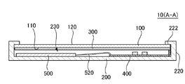
- 3 is a cross-sectional view taken along the line AA in FIG.
- the light emitting device 10 includes a first base material 100, a second base material 200, a light emitting element 300, and a control unit 400.
- the first base material 100 has flexibility and holds the light emitting element 300.
- the control unit 400 controls the light emitting element 300.
- the second substrate 200 has flexibility, and a part of the second substrate 200 is fixed to the first substrate 100, thereby forming a space partitioned between the first substrate 100. In this space, the controller 400 and the light emitting element 300 are located.
- the material of the second base material 200 is more flexible than the material of the first base material 100. Details will be described below.
- the first base material 100 is used as a substrate of the light emitting element 300.
- the first substrate 100 is formed using, for example, a translucent resin.
- a translucent resin for example, PEN (polyethylene naphthalate), PES (polyethersulfone), PET (polyethylene terephthalate), or polyimide can be used.
- the thickness of the 1st base material 100 is 200 micrometers or less, for example.
- at least the surface of the first base material 100 on which the light emitting element 300 is formed (the first surface 110, preferably the first surface).
- An inorganic barrier film such as SiN x or SiON is formed on both the first surface 110 and the second surface 120.
- the light emitting element 300 is an organic EL element, for example, and has a first electrode, a second electrode, and an organic layer.
- the first electrode is a transparent electrode having light transparency, and is located on the light emitting surface side of the light emitting element 300.
- the transparent conductive material constituting the transparent electrode is a metal-containing material, for example, a metal oxide such as ITO (Indium Tin Oxide), IZO (Indium Zinc Oxide), IWZO (Indium Tungsten Zinc Oxide), ZnO (Zinc Oxide) or the like. is there.
- the thickness of the first electrode is, for example, not less than 10 nm and not more than 500 nm.
- the first electrode is formed using, for example, a sputtering method or a vapor deposition method.
- the first electrode may be a carbon nanotube or a conductive organic material such as PEDOT / PSS.
- An auxiliary electrode may be provided on the first electrode.
- the auxiliary electrode is formed of, for example, MAM in which a Mo alloy layer, an Al alloy layer, and a Mo alloy layer are stacked in this order.
- the second electrode is, for example, a metal selected from the first group consisting of Al, Au, Ag, Pt, Mg, Sn, Zn, and In, or a metal consisting of an alloy of a metal selected from the first group. Contains layers. In this case, the second electrode has a light shielding property.
- the thickness of the second electrode is, for example, not less than 10 nm and not more than 500 nm. However, the second electrode may be formed using the material exemplified as the material of the first electrode.
- the second electrode is formed using, for example, a sputtering method or a vapor deposition method.
- the organic layer has, for example, a configuration in which a hole injection layer, a light emitting layer, and an electron injection layer are stacked in this order.
- a hole transport layer may be formed between the hole injection layer and the light emitting layer.
- an electron transport layer may be formed between the light emitting layer and the electron injection layer.
- an intermediate electrode formed of a material for forming the charge generation layer or the first electrode or the second electrode described above is provided between the light emitting layer and the light emitting layer.
- the organic layer may be formed by a vapor deposition method.
- At least one of the organic layers for example, a layer in contact with the first electrode may be formed by a coating method such as an inkjet method, a printing method, or a spray method.
- the remaining layers of the organic layer are formed by vapor deposition.
- all layers of the organic layer may be formed using a coating method.
- the light emitting element 300 has a first terminal and a second terminal.
- the first terminal is electrically connected to the first electrode, and the second terminal is electrically connected to the second electrode. These first terminal and second terminal are electrically connected to the control unit 400.
- the second substrate 200 has a polygonal shape such as a rectangle, for example, and has a recess 230 on a surface (one surface) facing the first substrate 100.
- the recess 230 is provided for arranging the control unit 400.
- at least a part of the portion of the one surface of the second base material 200 where the concave portion 230 is not formed is fixed to the first base material 100.
- the second base material 200 has a shape in which a side portion 220 protruding toward the first surface 110 side is provided on the entire periphery of the edge of the plate-like base material. Note that there may be a region where the side portion 220 is not provided on the edge of the second base material 200.
- the upper surface 222 of the side part 220 is flat, and is fixed to the part located in the circumference
- the surface of the first base material 100 that holds the light emitting element 300 faces the second base material 200. For this reason, the light emitting element 300 is located in the space described above.
- the second base material 200 has flexibility and is formed using a material having higher flexibility than the first base material 100.
- the material constituting the second substrate 200 is, for example, a silicone resin or polyurethane.
- the control unit 400 has a configuration in which, for example, a microcomputer and other electric elements are attached to a circuit board.
- the circuit board is preferably flexible. However, for example, when the circuit board is small, the circuit board may not have flexibility.
- the control unit 400 is mounted or fixed on a surface of the second base material 200 that faces the first base material 100.
- the battery 500 is accommodated in the space in which the control unit 400 is accommodated, that is, the space defined by the first base material 100 and the second base material 200.
- the battery 500 supplies power to the light emitting element 300 through the wiring 520 and the control unit 400.
- the battery 500 preferably has flexibility. However, for example, when the battery 500 is small, the battery 500 may not have flexibility.
- FIG. 4 is a cross-sectional view of the curved light emitting device 10.
- the joint between the first base material 100 and the second base material 200 (specifically, the edge of the first base material 100 and the upper surface 222 of the side part 220 of the second base material 200) Stress is generated at the joint). Then, strain is generated in the first base material 100 by this stress, and as a result, there is a possibility that stress is applied to the light emitting element 300.
- the side part 220 of the 2nd base material 200 is formed using the material softer than the 1st base material 100. FIG. Therefore, when the side part 220 is deformed, the stress applied to the first base material 100 is reduced. As a result, the stress applied to the light emitting element 300 can be reduced.
- the thickness of the first substrate 100 and the second substrate are set so that the curvature of the light emitting device 10 when the light emitting device 10 is applied with a force of about 300 N is such that the light emitting element 300 is not destroyed. At least one of the thicknesses of the material 200 is adjusted.
- the light emitting device 10 is curved in a direction in which a tensile stress is applied to the first base material 100 (that is, a direction in which the second surface 120 of the first base material 100 is convex).
- the light emitting device 10 may be curved in a direction in which a compressive stress is applied to the first base material 100 (that is, a direction in which the second surface 120 becomes concave).
- FIG. 5 is a cross-sectional view illustrating a configuration of the light-emitting device 10 according to the first modification
- FIG. 6 is a plan view of the light-emitting device 10 illustrated in FIG. FIG. 5 corresponds to FIG. 3 of the embodiment
- FIG. 6 corresponds to FIG. 1 of the embodiment.
- the light emitting device 10 according to this modification has the same configuration as the light emitting device 10 according to the embodiment except for the following points.
- the light emitting element 300 is formed not on the first base material 100 but on the third base material 600.
- the third substrate 600 is formed using, for example, PEN, PES, PET, or polyimide.
- the thickness of the third substrate 600 is, for example, 200 ⁇ m or less.
- the first base material 100 has a frame shape and is open except for the edges.
- the first base material 100 has the opening 130.
- the upper surface 222 of the side part 220 of the 2nd base material 200 is being fixed to the part located near the outer edge among the 1st surfaces 110 of the 1st base material 100, and the part located near the inner edge is the 1st.
- the edge part of the surface on the opposite side to the light emitting element 300 among the three base materials 600 is being fixed. Thereby, at least a part (all in the example of the drawing) of the opening 130 is blocked by the third base material 600.
- the light emitting element 300 overlaps the opening 130.
- the 1st base material 100 when the 1st base material 100 has translucency, the 1st base material 100 does not need to have the opening 130.
- FIG. In this case, the entire surface of the third substrate 600 is fixed to the first surface 110 of the first substrate 100.
- the stress applied to the light emitting element 300 when the light emitting device 10 is bent can be reduced.
- the first base material 100 since the light emitting element 300 is formed on the first base material 100, the first base material 100 is required to have high flatness, gas barrier properties, and the like. For this reason, the manufacturing cost of the 1st base material 100 becomes high.
- the third base material 600 since the light emitting element 300 is formed on the third base material 600, the third base material 600 is required to have high flatness, gas barrier properties, and the like.
- the area of the third substrate 600 is smaller than the area of the first substrate 100 in the embodiment. For this reason, the manufacturing cost of the 3rd base material 600 becomes lower than the manufacturing cost of the 1st base material 100 in an embodiment.
- flatness, gas barrier properties, and the like are not required for the first base material 100 in this modification. Therefore, the manufacturing cost of the 1st base material 100 in this modification is low. As a result, the manufacturing cost of the light emitting device 10 is lower than that of the embodiment.
- FIG. 7 is a cross-sectional view illustrating a configuration of the light emitting device 10 according to Modification Example 2, and corresponds to FIG. 3 in the embodiment.
- the upper part of the side portion 220 of the second base material 200 is bent toward the inside of the light emitting device 10 and is fixed to the second base material 100 while covering the edge of the second surface 120 of the first base material 100.
- the configuration is the same as that of the light emitting device 10 according to the embodiment.
- the side portion 220 may have the same structure as that in the present modification.
- the stress applied to the light emitting element 300 when the light emitting device 10 is bent can be reduced.
- the second surface 120 of the first base material 100 is located inside the light emitting device 10 with respect to the upper portion of the side portion 220 and the side surface of the first base material 100 is also covered with the side portion 220, It is possible to suppress the light emitting element 300 from being damaged due to the force applied to 100.
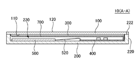
- FIG. 8 is a cross-sectional view illustrating a configuration of a light emitting device 10 according to Modification Example 3, and corresponds to FIG. 3 in the embodiment.
- the light-emitting device 10 according to the present modification has the light-emitting device 10 according to the embodiment except that a sheet-like member 700 is provided in a space defined by the first base material 100 and the second base material 200. It is the same composition as.
- the sheet-like member 700 has flexibility and is flat.
- the sheet-like member 700 is located between the control unit 400 and the battery 500 and the light emitting element 300. Thereby, when the light emitting device 10 is bent, it is possible to prevent the light emitting element 300 from being damaged by the control unit 400 or the battery 500 coming into contact with the light emitting element 300.
- the material that forms the sheet-like member 700 is preferably a material that is harder (less stretchable) than the material that forms the second substrate 200, such as PET.
- the stress applied to the light emitting element 300 when the light emitting device 10 is bent can be reduced for the same reason as in the embodiment.
- the cost of the method shown in this modification is lower, and the light emitting device 10 can be reduced in weight.
- the light emitting device 10 may include a sheet-like member 700.
- FIG. 9 is a cross-sectional view illustrating a configuration of a light emitting device 10 according to Modification Example 4, and corresponds to FIG. 3 in the embodiment.
- the light emitting device 10 according to this modification has the same configuration as the light emitting device 10 according to the embodiment except for the following points.
- the surface on which the microcomputer and the element are mounted on the circuit board of the control unit 400 faces the second substrate 200. Therefore, a flat surface of the control unit 400 faces the light emitting element 300.
- the recessed part 230 of the 2nd base material 200 is provided corresponding to each of the microcomputer of the battery 500 and the control part 400, and an element.
- the second base member 200 is provided with a recess 230 for storing the battery 500 and a recess 230 for storing the control unit 400 independently of each other.
- the stress applied to the light emitting element 300 when the light emitting device 10 is bent can be reduced. Further, since the flat surface of the control unit 400 faces the light emitting element 300, the light emitting element 300 can be prevented from being damaged by the control unit 400 when the light emitting device 10 is bent.
- the recess 230 may have the same configuration as in this modification.
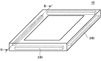
- FIG. 10 is a perspective view showing a configuration of a light emitting device 10 according to Modification 5
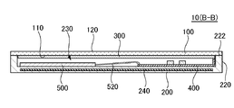
- FIG. 11 is a cross-sectional view taken along line BB of FIG.
- the light emitting device 10 according to the present modification has the same configuration as that of the embodiment or any one of the modifications 1 to 4 except that the shape maintaining member 240 is provided. In addition, this figure has shown the case similar to embodiment.
- the shape maintaining member 240 is a rod-shaped member and is embedded in the lower portion of the side portion 220 of the second base material 200.
- the shape maintaining member 240 is formed using a material that can be bent and can maintain the bent shape (for example, a metal material such as tin).
- the second base material 200 is a polygon (for example, a rectangle), and the shape maintaining member 240 is provided along each side of the second base material 200.
- at least one side of the second base material 200 may not have the shape maintaining member 240.
- the shape maintaining member 240 may have a shape (for example, an L shape) in which portions embedded in two adjacent sides of the second base material 200 are connected to each other, or an edge of the second base material 200 (For example, a rectangular frame in the case of a rectangle).
- a shape for example, an L shape
- portions embedded in two adjacent sides of the second base material 200 are connected to each other, or an edge of the second base material 200 (For example, a rectangular frame in the case of a rectangle).
- the shape maintenance member 240 is embedded in the 2nd base material 200 by being inserted in the hole provided in the 2nd base material 200, for example.
- a part (for example, the central portion) of the shape maintaining member 240 may be fixed (for example, bonded) to the second base member 200, and any part of the shape maintaining member 240 may be fixed to the second base member 200. It does not have to be. If it does in this way, compared with the case where the whole shape maintenance member 240 is being fixed to the 2nd substrate 200, the ease of bending of the 2nd substrate 200 can be maintained.
- the stress applied to the light emitting element 300 when the light emitting device 10 is bent can be reduced.
- the shape maintaining member 240 is bent when the light emitting device 10 is bent, the light emitting device 10 can maintain the bent state even if the force applied to the light emitting device 10 is zero.
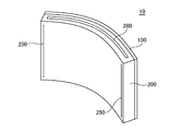
- FIG. 12 is a perspective view showing the configuration of the light emitting device 10 according to Modification 6. As shown in FIG. The light emitting device 10 according to this modification has the same configuration as that of the embodiment or any of modifications 1 to 5 except for the following points.
- the second substrate 200 has two grooves 250 and a slit 260.
- the two grooves 250 are formed on the surface of the second substrate 200 opposite to the first substrate 100 and are separated from each other.
- the second base material 200 is rectangular, and the groove 250 is formed along two sides of the second base material 200 that face each other.
- the slit 260 is formed in the side part 220 of the 2nd base material 200, and can accommodate the auxiliary member 252 (refer FIG. 13) inside.
- the slit 260 may pass through the part used as the baseplate of the 2nd base material 200, and may be connected with the space divided by the 1st base material 100 and the 2nd base material 200.
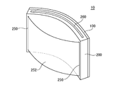
- FIG. 13 is a diagram showing how the auxiliary member 252 is used.
- the auxiliary member 252 is accommodated in the slit 260 and is taken out from the slit 260 when used.
- One end of the auxiliary member 252 is fixed to one groove 250, and the other end of the auxiliary member 252 is fixed to the remaining groove 250.
- the width of the auxiliary member 252 is narrower than the interval between the grooves 250. For this reason, by fixing the auxiliary member 252 to the groove 250, the light emitting device 10 is curved in a direction in which the first base material 100 is convex. Such a method of use is employed, for example, when the light emitting device 10 is a table lamp.
- FIG. 14 is a perspective view showing the configuration of the light emitting device 10 according to Modification 7. As shown in FIG. The light emitting device 10 according to this modification has the same configuration as that of Modification 6 except for the following points.
- the groove 250 is not provided in the second base material 200, and instead, the adhesive layer 254 is provided on the surface of the second base material 200 opposite to 100.
- the adhesive layer 254 is provided for attaching the light emitting device 10 to a wall or the like.
- the adhesive layer 254 is covered with a protective sheet 256.
- the protective sheet 256 is accommodated in the slit 260 after being peeled off from the adhesive layer 254. And after peeling the light-emitting device 10 from a wall etc., the adhesion layer 254 is again covered with the protective sheet 256.
- FIG. Such a method of use is employed, for example, when the light emitting device 10 is attached to or peeled off from a wall or the like.
Landscapes
- Engineering & Computer Science (AREA)
- General Engineering & Computer Science (AREA)
- Microelectronics & Electronic Packaging (AREA)
- Manufacturing & Machinery (AREA)
- Electroluminescent Light Sources (AREA)
- Fastening Of Light Sources Or Lamp Holders (AREA)
- Arrangement Of Elements, Cooling, Sealing, Or The Like Of Lighting Devices (AREA)
- Planar Illumination Modules (AREA)
Abstract
Description
前記第1基材に保持された発光素子と、
前記発光素子を制御する制御部と、
可撓性を有しており、一部が前記第1基材に固定されることにより、区画された空間を前記第1基材との間に形成する第2基材と、
を備え、
前記制御部は、前記空間内に位置しており、
前記第2基材の材料は、前記第1基材の材料よりも柔軟性が大きい発光装置である。
図5は、変形例1に係る発光装置10の構成を示す断面図であり、図6は図5に示した発光装置10の平面図である。図5は実施形態の図3に対応しており、図6は実施形態の図1に対応している。本変形例に係る発光装置10は、以下の点を除いて実施形態に係る発光装置10と同様の構成である。
図7は、変形例2に係る発光装置10の構成を示す断面図であり、実施形態における図3に対応している。本変形例に係る発光装置10は、第2基材200の側部220の上部が発光装置10の内側に向けて折れ曲がり、第1基材100の第2面120の縁を覆いつつここに固定されている点を除いて、実施形態に係る発光装置10と同様の構成である。なお、変形例1において、側部220が本変形例と同様の構造を有していてもよい。
図8は、変形例3に係る発光装置10の構成を示す断面図であり、実施形態における図3に対応している。本変形例に係る発光装置10は、第1基材100と第2基材200とで区画された空間内に、シート状部材700を備えている点を除いて、実施形態に係る発光装置10と同様の構成である。
図9は、変形例4に係る発光装置10の構成を示す断面図であり、実施形態における図3に対応している。本変形例に係る発光装置10は、以下の点を除いて実施形態に係る発光装置10と同様の構成である。
図10は、変形例5に係る発光装置10の構成を示す斜視図であり、図11は図10のB-B断面図である。本変形例に係る発光装置10は、形状維持部材240を有している点を除いて、実施形態又は変形例1~4のいずれかと同様の構成を有している。なお、本図は実施形態と同様の場合を示している。
図12は、変形例6に係る発光装置10の構成を示す斜視図である。本変形例に係る発光装置10は、以下の点を除いて実施形態又は変形例1~5のいずれかと同様の構成を有している。
図14は、変形例7に係る発光装置10の構成を示す斜視図である。本変形例に係る発光装置10は、以下の点を除いて変形例6と同様の構成を有している。
Claims (6)
- 可撓性を有する第1基材と、
前記第1基材に保持された発光素子と、
前記発光素子を制御する制御部と、
可撓性を有しており、一部が前記第1基材に固定されることにより、区画された空間を前記第1基材との間に形成する第2基材と、
を備え、
前記制御部は、前記空間内に位置しており、
前記第2基材の材料は、前記第1基材の材料よりも柔軟性が大きい発光装置。 - 請求項1に記載の発光装置において、
前記発光素子は前記空間内に位置する発光装置。 - 請求項1又は2に記載の発光装置において、
前記第2基材は一面側に凹部を有しており、かつ前記一面のうち前記凹部が形成されていない領域の少なくとも一部が前記第1基材に固定されており、
前記空間の少なくとも一部は前記凹部である発光装置。 - 請求項1~3のいずれか一項に記載の発光装置において、
前記第1基材は開口を有しており、
前記開口の少なくとも一部を塞いでいる第3基材を備え、
前記発光素子は前記第3基材に形成されており、かつ前記開口と重なっている発光装置。 - 請求項1~4のいずれか一項に記載の発光装置において、
前記第2基材は、当該第2基材の縁の少なくとも一部に、前記第1基材に向かって立ち上がっている側面部を備え、
前記側面部の上端の少なくとも一部は、前記第1基材を覆う方向に折れ曲がっており、
前記第1基材のうち前記空間に対向していない面の縁は、前記側面部の上端のうち前記折れ曲がっている部分に覆われている発光装置。 - 請求項1~5のいずれか一項に記載の発光装置において、
前記発光素子は、前記空間に位置しており、
さらに、前記発光素子と前記制御部の間に位置しており、可撓性を有するシート状部材を備える発光装置。
Priority Applications (3)
| Application Number | Priority Date | Filing Date | Title |
|---|---|---|---|
| PCT/JP2015/069059 WO2017002246A1 (ja) | 2015-07-01 | 2015-07-01 | 発光装置 |
| JP2017525759A JP6484712B2 (ja) | 2015-07-01 | 2015-07-01 | 発光装置 |
| US15/738,925 US20180212101A1 (en) | 2015-07-01 | 2015-07-01 | Light-emitting device |
Applications Claiming Priority (1)
| Application Number | Priority Date | Filing Date | Title |
|---|---|---|---|
| PCT/JP2015/069059 WO2017002246A1 (ja) | 2015-07-01 | 2015-07-01 | 発光装置 |
Publications (1)
| Publication Number | Publication Date |
|---|---|
| WO2017002246A1 true WO2017002246A1 (ja) | 2017-01-05 |
Family
ID=57608316
Family Applications (1)
| Application Number | Title | Priority Date | Filing Date |
|---|---|---|---|
| PCT/JP2015/069059 Ceased WO2017002246A1 (ja) | 2015-07-01 | 2015-07-01 | 発光装置 |
Country Status (3)
| Country | Link |
|---|---|
| US (1) | US20180212101A1 (ja) |
| JP (1) | JP6484712B2 (ja) |
| WO (1) | WO2017002246A1 (ja) |
Citations (5)
| Publication number | Priority date | Publication date | Assignee | Title |
|---|---|---|---|---|
| JP2010177049A (ja) * | 2009-01-29 | 2010-08-12 | Yamagata Promotional Organization For Industrial Technology | 照明装置 |
| JP2011090849A (ja) * | 2009-10-21 | 2011-05-06 | Atex Co Ltd | フレキシブル発光装置およびその製造方法 |
| JP2014024428A (ja) * | 2012-07-26 | 2014-02-06 | Mitsubishi Cable Ind Ltd | 警告表示灯 |
| JP2014127385A (ja) * | 2012-12-27 | 2014-07-07 | Nichia Chem Ind Ltd | 発光装置及びその製造方法 |
| JP2015513213A (ja) * | 2012-02-02 | 2015-04-30 | ザ プロクター アンド ギャンブルカンパニー | 二方向性光シート |
Family Cites Families (7)
| Publication number | Priority date | Publication date | Assignee | Title |
|---|---|---|---|---|
| US5856858A (en) * | 1997-12-01 | 1999-01-05 | The Regents Of The University Of California | Plastic substrates for active matrix liquid crystal display incapable of withstanding processing temperature of over 200° C and method of fabrication |
| US6483498B1 (en) * | 1999-03-17 | 2002-11-19 | International Business Machines Corporation | Liquid crystal display with integrated resistive touch sensor |
| JP5424451B2 (ja) * | 2008-11-21 | 2014-02-26 | パナソニック株式会社 | 照明器具 |
| JP2012099431A (ja) * | 2010-11-05 | 2012-05-24 | Konica Minolta Holdings Inc | 照明装置および発光パネル |
| US9866660B2 (en) * | 2011-03-21 | 2018-01-09 | Apple Inc. | Electronic devices with concave displays |
| US8929085B2 (en) * | 2011-09-30 | 2015-01-06 | Apple Inc. | Flexible electronic devices |
| JP6169861B2 (ja) * | 2013-03-01 | 2017-07-26 | 京セラ株式会社 | 液晶表示装置 |
-
2015
- 2015-07-01 JP JP2017525759A patent/JP6484712B2/ja active Active
- 2015-07-01 WO PCT/JP2015/069059 patent/WO2017002246A1/ja not_active Ceased
- 2015-07-01 US US15/738,925 patent/US20180212101A1/en not_active Abandoned
Patent Citations (5)
| Publication number | Priority date | Publication date | Assignee | Title |
|---|---|---|---|---|
| JP2010177049A (ja) * | 2009-01-29 | 2010-08-12 | Yamagata Promotional Organization For Industrial Technology | 照明装置 |
| JP2011090849A (ja) * | 2009-10-21 | 2011-05-06 | Atex Co Ltd | フレキシブル発光装置およびその製造方法 |
| JP2015513213A (ja) * | 2012-02-02 | 2015-04-30 | ザ プロクター アンド ギャンブルカンパニー | 二方向性光シート |
| JP2014024428A (ja) * | 2012-07-26 | 2014-02-06 | Mitsubishi Cable Ind Ltd | 警告表示灯 |
| JP2014127385A (ja) * | 2012-12-27 | 2014-07-07 | Nichia Chem Ind Ltd | 発光装置及びその製造方法 |
Also Published As
| Publication number | Publication date |
|---|---|
| JPWO2017002246A1 (ja) | 2018-04-19 |
| US20180212101A1 (en) | 2018-07-26 |
| JP6484712B2 (ja) | 2019-03-13 |
Similar Documents
| Publication | Publication Date | Title |
|---|---|---|
| JP6323806B2 (ja) | 発光デバイス及び移動体 | |
| JP6464854B2 (ja) | 面発光モジュール | |
| JP6484712B2 (ja) | 発光装置 | |
| JP2019071306A (ja) | 発光装置 | |
| JP2023065667A (ja) | 発光素子 | |
| WO2015079543A1 (ja) | 発光装置 | |
| JP6378769B2 (ja) | 光学装置 | |
| JP6512225B2 (ja) | 発光装置 | |
| JP6609939B2 (ja) | 発光装置 | |
| EP2913860B1 (en) | Lighting panel | |
| WO2016152268A1 (ja) | 発光装置 | |
| JPWO2018151027A1 (ja) | 発光装置 | |
| JP2017062965A (ja) | 発光装置 | |
| JP2023053241A (ja) | 発光装置 | |
| JP2016119200A (ja) | 発光装置 | |
| JP2023065544A (ja) | 発光装置 | |
| JP2018156722A (ja) | 有機elパネル | |
| WO2017163331A1 (ja) | 発光装置、電子装置および発光装置の製造方法 | |
| JPWO2016208430A1 (ja) | 有機elデバイス、有機el照明パネル、有機el照明装置および有機elディスプレイ | |
| JP2016184539A (ja) | 発光装置 | |
| JP6294071B2 (ja) | 発光装置 | |
| JP2016091930A (ja) | 発光装置 | |
| JP2016066540A (ja) | 発光装置 | |
| WO2016046914A1 (ja) | 発光装置 | |
| US20160293882A1 (en) | OLED Illuminating Device |
Legal Events
| Date | Code | Title | Description |
|---|---|---|---|
| 121 | Ep: the epo has been informed by wipo that ep was designated in this application |
Ref document number: 15897173 Country of ref document: EP Kind code of ref document: A1 |
|
| ENP | Entry into the national phase |
Ref document number: 2017525759 Country of ref document: JP Kind code of ref document: A |
|
| NENP | Non-entry into the national phase |
Ref country code: DE |
|
| WWE | Wipo information: entry into national phase |
Ref document number: 15738925 Country of ref document: US |
|
| 122 | Ep: pct application non-entry in european phase |
Ref document number: 15897173 Country of ref document: EP Kind code of ref document: A1 |