WO2016208122A1 - 半導体チップおよびそれを用いた半導体モジュール - Google Patents
半導体チップおよびそれを用いた半導体モジュール Download PDFInfo
- Publication number
- WO2016208122A1 WO2016208122A1 PCT/JP2016/002581 JP2016002581W WO2016208122A1 WO 2016208122 A1 WO2016208122 A1 WO 2016208122A1 JP 2016002581 W JP2016002581 W JP 2016002581W WO 2016208122 A1 WO2016208122 A1 WO 2016208122A1
- Authority
- WO
- WIPO (PCT)
- Prior art keywords
- control
- semiconductor chip
- pad
- terminal
- pads
- Prior art date
- Legal status (The legal status is an assumption and is not a legal conclusion. Google has not performed a legal analysis and makes no representation as to the accuracy of the status listed.)
- Ceased
Links
Images


Classifications
-
- H—ELECTRICITY
- H10—SEMICONDUCTOR DEVICES; ELECTRIC SOLID-STATE DEVICES NOT OTHERWISE PROVIDED FOR
- H10W—GENERIC PACKAGES, INTERCONNECTIONS, CONNECTORS OR OTHER CONSTRUCTIONAL DETAILS OF DEVICES COVERED BY CLASS H10
- H10W90/00—Package configurations
-
- H—ELECTRICITY
- H02—GENERATION; CONVERSION OR DISTRIBUTION OF ELECTRIC POWER
- H02M—APPARATUS FOR CONVERSION BETWEEN AC AND AC, BETWEEN AC AND DC, OR BETWEEN DC AND DC, AND FOR USE WITH MAINS OR SIMILAR POWER SUPPLY SYSTEMS; CONVERSION OF DC OR AC INPUT POWER INTO SURGE OUTPUT POWER; CONTROL OR REGULATION THEREOF
- H02M7/00—Conversion of AC power input into DC power output; Conversion of DC power input into AC power output
- H02M7/003—Constructional details, e.g. physical layout, assembly, wiring or busbar connections
-
- H—ELECTRICITY
- H10—SEMICONDUCTOR DEVICES; ELECTRIC SOLID-STATE DEVICES NOT OTHERWISE PROVIDED FOR
- H10D—INORGANIC ELECTRIC SEMICONDUCTOR DEVICES
- H10D12/00—Bipolar devices controlled by the field effect, e.g. insulated-gate bipolar transistors [IGBT]
- H10D12/411—Insulated-gate bipolar transistors [IGBT]
- H10D12/441—Vertical IGBTs
- H10D12/461—Vertical IGBTs having non-planar surfaces, e.g. having trenches, recesses or pillars in the surfaces of the emitter, base or collector regions
- H10D12/481—Vertical IGBTs having non-planar surfaces, e.g. having trenches, recesses or pillars in the surfaces of the emitter, base or collector regions having gate structures on slanted surfaces, on vertical surfaces, or in grooves, e.g. trench gate IGBTs
-
- H—ELECTRICITY
- H10—SEMICONDUCTOR DEVICES; ELECTRIC SOLID-STATE DEVICES NOT OTHERWISE PROVIDED FOR
- H10D—INORGANIC ELECTRIC SEMICONDUCTOR DEVICES
- H10D62/00—Semiconductor bodies, or regions thereof, of devices having potential barriers
- H10D62/10—Shapes, relative sizes or dispositions of the regions of the semiconductor bodies; Shapes of the semiconductor bodies
- H10D62/124—Shapes, relative sizes or dispositions of the regions of semiconductor bodies or of junctions between the regions
- H10D62/126—Top-view geometrical layouts of the regions or the junctions
- H10D62/127—Top-view geometrical layouts of the regions or the junctions of cellular field-effect devices, e.g. multicellular DMOS transistors or IGBTs
-
- H—ELECTRICITY
- H10—SEMICONDUCTOR DEVICES; ELECTRIC SOLID-STATE DEVICES NOT OTHERWISE PROVIDED FOR
- H10D—INORGANIC ELECTRIC SEMICONDUCTOR DEVICES
- H10D62/00—Semiconductor bodies, or regions thereof, of devices having potential barriers
- H10D62/10—Shapes, relative sizes or dispositions of the regions of the semiconductor bodies; Shapes of the semiconductor bodies
- H10D62/13—Semiconductor regions connected to electrodes carrying current to be rectified, amplified or switched, e.g. source or drain regions
- H10D62/141—Anode or cathode regions of thyristors; Collector or emitter regions of gated bipolar-mode devices, e.g. of IGBTs
- H10D62/142—Anode regions of thyristors or collector regions of gated bipolar-mode devices
-
- H—ELECTRICITY
- H10—SEMICONDUCTOR DEVICES; ELECTRIC SOLID-STATE DEVICES NOT OTHERWISE PROVIDED FOR
- H10D—INORGANIC ELECTRIC SEMICONDUCTOR DEVICES
- H10D64/00—Electrodes of devices having potential barriers
- H10D64/111—Field plates
- H10D64/117—Recessed field plates, e.g. trench field plates or buried field plates
-
- H—ELECTRICITY
- H10—SEMICONDUCTOR DEVICES; ELECTRIC SOLID-STATE DEVICES NOT OTHERWISE PROVIDED FOR
- H10D—INORGANIC ELECTRIC SEMICONDUCTOR DEVICES
- H10D84/00—Integrated devices formed in or on semiconductor substrates that comprise only semiconducting layers, e.g. on Si wafers or on GaAs-on-Si wafers
- H10D84/40—Integrated devices formed in or on semiconductor substrates that comprise only semiconducting layers, e.g. on Si wafers or on GaAs-on-Si wafers characterised by the integration of at least one component covered by groups H10D12/00 or H10D30/00 with at least one component covered by groups H10D10/00 or H10D18/00, e.g. integration of IGFETs with BJTs
- H10D84/401—Combinations of FETs or IGBTs with BJTs
- H10D84/403—Combinations of FETs or IGBTs with BJTs and with one or more of diodes, resistors or capacitors
-
- H—ELECTRICITY
- H10—SEMICONDUCTOR DEVICES; ELECTRIC SOLID-STATE DEVICES NOT OTHERWISE PROVIDED FOR
- H10D—INORGANIC ELECTRIC SEMICONDUCTOR DEVICES
- H10D84/00—Integrated devices formed in or on semiconductor substrates that comprise only semiconducting layers, e.g. on Si wafers or on GaAs-on-Si wafers
- H10D84/80—Integrated devices formed in or on semiconductor substrates that comprise only semiconducting layers, e.g. on Si wafers or on GaAs-on-Si wafers characterised by the integration of at least one component covered by groups H10D12/00 or H10D30/00, e.g. integration of IGFETs
- H10D84/811—Combinations of field-effect devices and one or more diodes, capacitors or resistors
-
- H—ELECTRICITY
- H10—SEMICONDUCTOR DEVICES; ELECTRIC SOLID-STATE DEVICES NOT OTHERWISE PROVIDED FOR
- H10W—GENERIC PACKAGES, INTERCONNECTIONS, CONNECTORS OR OTHER CONSTRUCTIONAL DETAILS OF DEVICES COVERED BY CLASS H10
- H10W40/00—Arrangements for thermal protection or thermal control
- H10W40/20—Arrangements for cooling
- H10W40/22—Arrangements for cooling characterised by their shape, e.g. having conical or cylindrical projections
-
- H—ELECTRICITY
- H10—SEMICONDUCTOR DEVICES; ELECTRIC SOLID-STATE DEVICES NOT OTHERWISE PROVIDED FOR
- H10W—GENERIC PACKAGES, INTERCONNECTIONS, CONNECTORS OR OTHER CONSTRUCTIONAL DETAILS OF DEVICES COVERED BY CLASS H10
- H10W40/00—Arrangements for thermal protection or thermal control
- H10W40/70—Fillings or auxiliary members in containers or in encapsulations for thermal protection or control
- H10W40/77—Auxiliary members characterised by their shape
- H10W40/778—Auxiliary members characterised by their shape in encapsulations
-
- H—ELECTRICITY
- H10—SEMICONDUCTOR DEVICES; ELECTRIC SOLID-STATE DEVICES NOT OTHERWISE PROVIDED FOR
- H10W—GENERIC PACKAGES, INTERCONNECTIONS, CONNECTORS OR OTHER CONSTRUCTIONAL DETAILS OF DEVICES COVERED BY CLASS H10
- H10W70/00—Package substrates; Interposers; Redistribution layers [RDL]
- H10W70/40—Leadframes
- H10W70/421—Shapes or dispositions
-
- H—ELECTRICITY
- H10—SEMICONDUCTOR DEVICES; ELECTRIC SOLID-STATE DEVICES NOT OTHERWISE PROVIDED FOR
- H10W—GENERIC PACKAGES, INTERCONNECTIONS, CONNECTORS OR OTHER CONSTRUCTIONAL DETAILS OF DEVICES COVERED BY CLASS H10
- H10W70/00—Package substrates; Interposers; Redistribution layers [RDL]
- H10W70/40—Leadframes
- H10W70/481—Leadframes for devices being provided for in groups H10D8/00 - H10D48/00
-
- H—ELECTRICITY
- H10—SEMICONDUCTOR DEVICES; ELECTRIC SOLID-STATE DEVICES NOT OTHERWISE PROVIDED FOR
- H10W—GENERIC PACKAGES, INTERCONNECTIONS, CONNECTORS OR OTHER CONSTRUCTIONAL DETAILS OF DEVICES COVERED BY CLASS H10
- H10W72/00—Interconnections or connectors in packages
- H10W72/90—Bond pads, in general
-
- H—ELECTRICITY
- H10—SEMICONDUCTOR DEVICES; ELECTRIC SOLID-STATE DEVICES NOT OTHERWISE PROVIDED FOR
- H10W—GENERIC PACKAGES, INTERCONNECTIONS, CONNECTORS OR OTHER CONSTRUCTIONAL DETAILS OF DEVICES COVERED BY CLASS H10
- H10W90/00—Package configurations
- H10W90/811—Multiple chips on leadframes
-
- H—ELECTRICITY
- H02—GENERATION; CONVERSION OR DISTRIBUTION OF ELECTRIC POWER
- H02M—APPARATUS FOR CONVERSION BETWEEN AC AND AC, BETWEEN AC AND DC, OR BETWEEN DC AND DC, AND FOR USE WITH MAINS OR SIMILAR POWER SUPPLY SYSTEMS; CONVERSION OF DC OR AC INPUT POWER INTO SURGE OUTPUT POWER; CONTROL OR REGULATION THEREOF
- H02M1/00—Details of apparatus for conversion
- H02M1/32—Means for protecting converters other than automatic disconnection
- H02M1/327—Means for protecting converters other than automatic disconnection against abnormal temperatures
-
- H—ELECTRICITY
- H02—GENERATION; CONVERSION OR DISTRIBUTION OF ELECTRIC POWER
- H02M—APPARATUS FOR CONVERSION BETWEEN AC AND AC, BETWEEN AC AND DC, OR BETWEEN DC AND DC, AND FOR USE WITH MAINS OR SIMILAR POWER SUPPLY SYSTEMS; CONVERSION OF DC OR AC INPUT POWER INTO SURGE OUTPUT POWER; CONTROL OR REGULATION THEREOF
- H02M7/00—Conversion of AC power input into DC power output; Conversion of DC power input into AC power output
- H02M7/42—Conversion of DC power input into AC power output without possibility of reversal
- H02M7/44—Conversion of DC power input into AC power output without possibility of reversal by static converters
- H02M7/48—Conversion of DC power input into AC power output without possibility of reversal by static converters using discharge tubes with control electrode or semiconductor devices with control electrode
- H02M7/53—Conversion of DC power input into AC power output without possibility of reversal by static converters using discharge tubes with control electrode or semiconductor devices with control electrode using devices of a triode or transistor type requiring continuous application of a control signal
- H02M7/537—Conversion of DC power input into AC power output without possibility of reversal by static converters using discharge tubes with control electrode or semiconductor devices with control electrode using devices of a triode or transistor type requiring continuous application of a control signal using semiconductor devices only, e.g. single switched pulse inverters
- H02M7/5387—Conversion of DC power input into AC power output without possibility of reversal by static converters using discharge tubes with control electrode or semiconductor devices with control electrode using devices of a triode or transistor type requiring continuous application of a control signal using semiconductor devices only, e.g. single switched pulse inverters in a bridge configuration
-
- H—ELECTRICITY
- H02—GENERATION; CONVERSION OR DISTRIBUTION OF ELECTRIC POWER
- H02P—CONTROL OR REGULATION OF ELECTRIC MOTORS, ELECTRIC GENERATORS OR DYNAMO-ELECTRIC CONVERTERS; CONTROLLING TRANSFORMERS, REACTORS OR CHOKE COILS
- H02P27/00—Arrangements or methods for the control of AC motors characterised by the kind of supply voltage
- H02P27/04—Arrangements or methods for the control of AC motors characterised by the kind of supply voltage using variable-frequency supply voltage, e.g. inverter or converter supply voltage
- H02P27/06—Arrangements or methods for the control of AC motors characterised by the kind of supply voltage using variable-frequency supply voltage, e.g. inverter or converter supply voltage using DC to AC converters or inverters
-
- H—ELECTRICITY
- H02—GENERATION; CONVERSION OR DISTRIBUTION OF ELECTRIC POWER
- H02P—CONTROL OR REGULATION OF ELECTRIC MOTORS, ELECTRIC GENERATORS OR DYNAMO-ELECTRIC CONVERTERS; CONTROLLING TRANSFORMERS, REACTORS OR CHOKE COILS
- H02P31/00—Arrangements for regulating or controlling electric motors not provided for in groups H02P1/00 - H02P5/00, H02P7/00 or H02P21/00 - H02P29/00
-
- H—ELECTRICITY
- H10—SEMICONDUCTOR DEVICES; ELECTRIC SOLID-STATE DEVICES NOT OTHERWISE PROVIDED FOR
- H10D—INORGANIC ELECTRIC SEMICONDUCTOR DEVICES
- H10D62/00—Semiconductor bodies, or regions thereof, of devices having potential barriers
- H10D62/10—Shapes, relative sizes or dispositions of the regions of the semiconductor bodies; Shapes of the semiconductor bodies
- H10D62/13—Semiconductor regions connected to electrodes carrying current to be rectified, amplified or switched, e.g. source or drain regions
- H10D62/133—Emitter regions of BJTs
-
- H—ELECTRICITY
- H10—SEMICONDUCTOR DEVICES; ELECTRIC SOLID-STATE DEVICES NOT OTHERWISE PROVIDED FOR
- H10D—INORGANIC ELECTRIC SEMICONDUCTOR DEVICES
- H10D62/00—Semiconductor bodies, or regions thereof, of devices having potential barriers
- H10D62/10—Shapes, relative sizes or dispositions of the regions of the semiconductor bodies; Shapes of the semiconductor bodies
- H10D62/13—Semiconductor regions connected to electrodes carrying current to be rectified, amplified or switched, e.g. source or drain regions
- H10D62/137—Collector regions of BJTs
-
- H—ELECTRICITY
- H10—SEMICONDUCTOR DEVICES; ELECTRIC SOLID-STATE DEVICES NOT OTHERWISE PROVIDED FOR
- H10D—INORGANIC ELECTRIC SEMICONDUCTOR DEVICES
- H10D62/00—Semiconductor bodies, or regions thereof, of devices having potential barriers
- H10D62/10—Shapes, relative sizes or dispositions of the regions of the semiconductor bodies; Shapes of the semiconductor bodies
- H10D62/17—Semiconductor regions connected to electrodes not carrying current to be rectified, amplified or switched, e.g. channel regions
- H10D62/177—Base regions of bipolar transistors, e.g. BJTs or IGBTs
-
- H—ELECTRICITY
- H10—SEMICONDUCTOR DEVICES; ELECTRIC SOLID-STATE DEVICES NOT OTHERWISE PROVIDED FOR
- H10D—INORGANIC ELECTRIC SEMICONDUCTOR DEVICES
- H10D62/00—Semiconductor bodies, or regions thereof, of devices having potential barriers
- H10D62/10—Shapes, relative sizes or dispositions of the regions of the semiconductor bodies; Shapes of the semiconductor bodies
- H10D62/17—Semiconductor regions connected to electrodes not carrying current to be rectified, amplified or switched, e.g. channel regions
- H10D62/393—Body regions of DMOS transistors or IGBTs
-
- H—ELECTRICITY
- H10—SEMICONDUCTOR DEVICES; ELECTRIC SOLID-STATE DEVICES NOT OTHERWISE PROVIDED FOR
- H10D—INORGANIC ELECTRIC SEMICONDUCTOR DEVICES
- H10D8/00—Diodes
- H10D8/422—PN diodes having the PN junctions in mesas
-
- H—ELECTRICITY
- H10—SEMICONDUCTOR DEVICES; ELECTRIC SOLID-STATE DEVICES NOT OTHERWISE PROVIDED FOR
- H10W—GENERIC PACKAGES, INTERCONNECTIONS, CONNECTORS OR OTHER CONSTRUCTIONAL DETAILS OF DEVICES COVERED BY CLASS H10
- H10W72/00—Interconnections or connectors in packages
- H10W72/071—Connecting or disconnecting
- H10W72/073—Connecting or disconnecting of die-attach connectors
- H10W72/07351—Connecting or disconnecting of die-attach connectors characterised by changes in properties of the die-attach connectors during connecting
-
- H—ELECTRICITY
- H10—SEMICONDUCTOR DEVICES; ELECTRIC SOLID-STATE DEVICES NOT OTHERWISE PROVIDED FOR
- H10W—GENERIC PACKAGES, INTERCONNECTIONS, CONNECTORS OR OTHER CONSTRUCTIONAL DETAILS OF DEVICES COVERED BY CLASS H10
- H10W72/00—Interconnections or connectors in packages
- H10W72/071—Connecting or disconnecting
- H10W72/073—Connecting or disconnecting of die-attach connectors
- H10W72/07351—Connecting or disconnecting of die-attach connectors characterised by changes in properties of the die-attach connectors during connecting
- H10W72/07354—Connecting or disconnecting of die-attach connectors characterised by changes in properties of the die-attach connectors during connecting changes in dispositions
-
- H—ELECTRICITY
- H10—SEMICONDUCTOR DEVICES; ELECTRIC SOLID-STATE DEVICES NOT OTHERWISE PROVIDED FOR
- H10W—GENERIC PACKAGES, INTERCONNECTIONS, CONNECTORS OR OTHER CONSTRUCTIONAL DETAILS OF DEVICES COVERED BY CLASS H10
- H10W72/00—Interconnections or connectors in packages
- H10W72/071—Connecting or disconnecting
- H10W72/075—Connecting or disconnecting of bond wires
- H10W72/07551—Connecting or disconnecting of bond wires characterised by changes in properties of the bond wires during the connecting
- H10W72/07554—Connecting or disconnecting of bond wires characterised by changes in properties of the bond wires during the connecting changes in dispositions
-
- H—ELECTRICITY
- H10—SEMICONDUCTOR DEVICES; ELECTRIC SOLID-STATE DEVICES NOT OTHERWISE PROVIDED FOR
- H10W—GENERIC PACKAGES, INTERCONNECTIONS, CONNECTORS OR OTHER CONSTRUCTIONAL DETAILS OF DEVICES COVERED BY CLASS H10
- H10W72/00—Interconnections or connectors in packages
- H10W72/30—Die-attach connectors
-
- H—ELECTRICITY
- H10—SEMICONDUCTOR DEVICES; ELECTRIC SOLID-STATE DEVICES NOT OTHERWISE PROVIDED FOR
- H10W—GENERIC PACKAGES, INTERCONNECTIONS, CONNECTORS OR OTHER CONSTRUCTIONAL DETAILS OF DEVICES COVERED BY CLASS H10
- H10W72/00—Interconnections or connectors in packages
- H10W72/30—Die-attach connectors
- H10W72/341—Dispositions of die-attach connectors, e.g. layouts
- H10W72/347—Dispositions of multiple die-attach connectors
-
- H—ELECTRICITY
- H10—SEMICONDUCTOR DEVICES; ELECTRIC SOLID-STATE DEVICES NOT OTHERWISE PROVIDED FOR
- H10W—GENERIC PACKAGES, INTERCONNECTIONS, CONNECTORS OR OTHER CONSTRUCTIONAL DETAILS OF DEVICES COVERED BY CLASS H10
- H10W72/00—Interconnections or connectors in packages
- H10W72/30—Die-attach connectors
- H10W72/351—Materials of die-attach connectors
- H10W72/352—Materials of die-attach connectors comprising metals or metalloids, e.g. solders
-
- H—ELECTRICITY
- H10—SEMICONDUCTOR DEVICES; ELECTRIC SOLID-STATE DEVICES NOT OTHERWISE PROVIDED FOR
- H10W—GENERIC PACKAGES, INTERCONNECTIONS, CONNECTORS OR OTHER CONSTRUCTIONAL DETAILS OF DEVICES COVERED BY CLASS H10
- H10W72/00—Interconnections or connectors in packages
- H10W72/50—Bond wires
-
- H—ELECTRICITY
- H10—SEMICONDUCTOR DEVICES; ELECTRIC SOLID-STATE DEVICES NOT OTHERWISE PROVIDED FOR
- H10W—GENERIC PACKAGES, INTERCONNECTIONS, CONNECTORS OR OTHER CONSTRUCTIONAL DETAILS OF DEVICES COVERED BY CLASS H10
- H10W72/00—Interconnections or connectors in packages
- H10W72/50—Bond wires
- H10W72/59—Bond pads specially adapted therefor
-
- H—ELECTRICITY
- H10—SEMICONDUCTOR DEVICES; ELECTRIC SOLID-STATE DEVICES NOT OTHERWISE PROVIDED FOR
- H10W—GENERIC PACKAGES, INTERCONNECTIONS, CONNECTORS OR OTHER CONSTRUCTIONAL DETAILS OF DEVICES COVERED BY CLASS H10
- H10W72/00—Interconnections or connectors in packages
- H10W72/851—Dispositions of multiple connectors or interconnections
- H10W72/853—On the same surface
- H10W72/865—Die-attach connectors and bond wires
-
- H—ELECTRICITY
- H10—SEMICONDUCTOR DEVICES; ELECTRIC SOLID-STATE DEVICES NOT OTHERWISE PROVIDED FOR
- H10W—GENERIC PACKAGES, INTERCONNECTIONS, CONNECTORS OR OTHER CONSTRUCTIONAL DETAILS OF DEVICES COVERED BY CLASS H10
- H10W72/00—Interconnections or connectors in packages
- H10W72/851—Dispositions of multiple connectors or interconnections
- H10W72/874—On different surfaces
- H10W72/884—Die-attach connectors and bond wires
-
- H—ELECTRICITY
- H10—SEMICONDUCTOR DEVICES; ELECTRIC SOLID-STATE DEVICES NOT OTHERWISE PROVIDED FOR
- H10W—GENERIC PACKAGES, INTERCONNECTIONS, CONNECTORS OR OTHER CONSTRUCTIONAL DETAILS OF DEVICES COVERED BY CLASS H10
- H10W72/00—Interconnections or connectors in packages
- H10W72/90—Bond pads, in general
- H10W72/921—Structures or relative sizes of bond pads
- H10W72/926—Multiple bond pads having different sizes
-
- H—ELECTRICITY
- H10—SEMICONDUCTOR DEVICES; ELECTRIC SOLID-STATE DEVICES NOT OTHERWISE PROVIDED FOR
- H10W—GENERIC PACKAGES, INTERCONNECTIONS, CONNECTORS OR OTHER CONSTRUCTIONAL DETAILS OF DEVICES COVERED BY CLASS H10
- H10W74/00—Encapsulations, e.g. protective coatings
-
- H—ELECTRICITY
- H10—SEMICONDUCTOR DEVICES; ELECTRIC SOLID-STATE DEVICES NOT OTHERWISE PROVIDED FOR
- H10W—GENERIC PACKAGES, INTERCONNECTIONS, CONNECTORS OR OTHER CONSTRUCTIONAL DETAILS OF DEVICES COVERED BY CLASS H10
- H10W90/00—Package configurations
- H10W90/701—Package configurations characterised by the relative positions of pads or connectors relative to package parts
- H10W90/731—Package configurations characterised by the relative positions of pads or connectors relative to package parts of die-attach connectors
- H10W90/736—Package configurations characterised by the relative positions of pads or connectors relative to package parts of die-attach connectors between a chip and a stacked lead frame, conducting package substrate or heat sink
-
- H—ELECTRICITY
- H10—SEMICONDUCTOR DEVICES; ELECTRIC SOLID-STATE DEVICES NOT OTHERWISE PROVIDED FOR
- H10W—GENERIC PACKAGES, INTERCONNECTIONS, CONNECTORS OR OTHER CONSTRUCTIONAL DETAILS OF DEVICES COVERED BY CLASS H10
- H10W90/00—Package configurations
- H10W90/701—Package configurations characterised by the relative positions of pads or connectors relative to package parts
- H10W90/751—Package configurations characterised by the relative positions of pads or connectors relative to package parts of bond wires
- H10W90/756—Package configurations characterised by the relative positions of pads or connectors relative to package parts of bond wires between a chip and a stacked lead frame, conducting package substrate or heat sink
Definitions
- the present disclosure relates to a semiconductor chip having a plurality of pads connected to control terminals and a semiconductor module using the semiconductor chip.
- Patent Document 1 proposes a semiconductor module having a so-called 2-in-1 structure as a semiconductor module constituting an inverter. That is, this semiconductor module includes a semiconductor chip having a switching element constituting the upper arm and a semiconductor chip having a switching element constituting the lower arm, and the switching elements of the respective semiconductor chips are connected in series. In this semiconductor module, the configuration of each semiconductor chip is common, and an IGBT element is formed respectively.
- An upper heat sink is disposed on the emitter side of the semiconductor chip on which the IGBT element is formed, and a lower heat sink is disposed on the collector side.
- the upper heat sink on the upper arm side and the lower heat sink on the lower arm side, Is connected, the switching element of the upper arm and the switching element of the lower arm are electrically connected.
- the lower heat sink on the upper arm side is connected to the first main terminal (positive terminal)
- the lower heat sink on the lower arm side is connected to the second main terminal (output terminal)
- the upper heat sink on the lower arm side is The third main terminal (negative electrode terminal) is connected.
- the first to third main terminals When viewed from above the upper heat sink, the first to third main terminals extend in the same direction with respect to the semiconductor chip, and if the distance between the first main terminal and the third main terminal is increased, the parasitic inductance is increased. Since it becomes large, a 3rd main terminal is arrange
- Each semiconductor chip has a gate pad and a Kelvin emitter pad as control pads for controlling the IGBT elements formed in each semiconductor chip.
- Each control pad is electrically connected to the gate terminal and the Kelvin emitter terminal.
- the semiconductor module semiconductor chip
- the IGBT element when a predetermined voltage is applied to the gate pad and the IGBT element is turned on, a magnetic flux is induced based on the main current flowing between the main terminals. . Since a control current (inductive current) is generated between the gate terminal and the Kelvin emitter terminal so as to prevent the induced magnetic flux, the voltage applied to the gate pad varies.
- the third main terminal is disposed between the first main terminal and the second main terminal, the direction in which the main current flows from the first main terminal to the second main terminal, The direction in which the main current flows from the main terminal to the third main terminal is reversed. That is, the control currents generated in the upper arm semiconductor chip and the lower arm semiconductor chip are reversed.
- the control current flows from the Kelvin emitter terminal to the gate terminal side, and the other semiconductor chip.
- a control current flows from the gate terminal to the Kelvin emitter terminal side.
- the voltage applied to the gate pad increases to the side where the IGBT element is turned on, resulting in malfunction.
- an object of the present disclosure is to provide a semiconductor chip that can prevent a switching element from malfunctioning and a semiconductor module using the semiconductor chip.
- a semiconductor chip includes a plurality of pads and a switching element having a gate electrode.
- the plurality of pads are electrically connected to the gate electrode, and a control current is applied between the first control pad to which a voltage for controlling on / off of the switching element is applied and the first control pad when the switching element is on.
- a second control pad that constitutes a current path through which the first control pad and the second control pad are arranged such that either one of the control pads is sandwiched between the other control pads.
- the arrangement of the control terminals connected to the first control pad and the second control pad can be appropriately changed. That is, the control terminal can be connected to the first control pad and the second control pad so that the control current flows from the second control pad to the first control pad. Therefore, it is possible to prevent the switching element from malfunctioning due to the control current.
- the semiconductor module includes a switching element having a gate electrode, a first main pad formed on the front surface, a plurality of control pads adjacent to each other, and a second main pad formed on the back surface.
- a pad is formed, a first semiconductor chip constituting the upper arm, a switching element having a gate electrode is formed, and the first semiconductor chip is configured in common, and is arranged adjacent to the first semiconductor chip.
- the second semiconductor chip constituting the lower arm, the positive terminal electrically connected to the second main pad of the first semiconductor chip, and the first main pad of the second semiconductor chip.
- the positive terminal, the negative terminal, and the output terminal extend in the same direction with respect to the first semiconductor chip and the second semiconductor chip.
- a negative electrode terminal is disposed between the positive electrode terminal and the output terminal, the plurality of control pads are electrically connected to the gate electrode, and a first control pad to which a voltage for controlling on / off of the switching element is applied.
- a second control pad that constitutes a current path through which a control current flows to and from the first control pad when the switching element is on, and the first control pad and the second control pad are either
- the pad is disposed between the other pads
- the control terminal has a first control terminal connected to the first control pad, and a second control terminal connected to the second control pad, 1st system
- the terminal and the second control terminal are electrically connected to the first control pad and the second control pad in the first semiconductor chip and the second semiconductor chip, respectively, so that the control current flows from the second control terminal toward the first control terminal. It is connected to the.
- the first control terminal and the second control terminal respectively perform the first control so that the control current flows from the second control terminal toward the first control terminal.
- the pad and the second control pad are electrically connected.
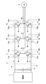
- FIG. 1 is a circuit diagram of an inverter configured by applying the semiconductor module according to the first embodiment.
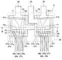
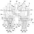
- FIG. 2 is a schematic plan view of the semiconductor module.
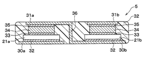
- 3 is a cross-sectional view corresponding to the III-III cross section in FIG.
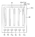
- FIG. 4 is a plan view of the semiconductor chip.
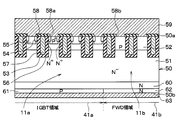
- FIG. 5 is a cross-sectional view corresponding to the VV cross section in FIG.
- FIG. 6A is a diagram illustrating the flow direction of the control current in the upper arm.
- FIG. 6B is a diagram illustrating the flow direction of the control current in the lower arm.
- FIG. 7 is a plan view of a semiconductor chip in the second embodiment.
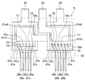
- FIG. 8 is a plan view of the semiconductor module according to the third embodiment.
- the inverter is for AC driving a three-phase motor 4 that is a load based on a DC power supply.
- the inverter includes a power supply unit 1 including a booster circuit, an inverter output circuit 2, a power supply unit 1 and an inverter output circuit 2. And a capacitor 3 arranged in parallel therebetween.
- the capacitor 3 is a smoothing capacitor and is provided to suppress the influence of noise of the power supply unit (boost circuit) 1 and form a constant power supply voltage.
- the inverter output circuit 2 has a configuration in which upper and lower arms 11 to 16 connected in series are connected in parallel for three phases, and an intermediate potential between the upper arms 11, 13, 15 and the lower arms 12, 14, 16 is set to the three-phase motor 4.
- the upper and lower arms 11 to 16 include IGBT elements 11a to 16a and FWD (free wheel diode) elements 11b to 16b, respectively, and the IGBT elements 11a to 16a of the upper and lower arms 11 to 16 of each phase are controlled on and off.
- a three-phase alternating current having a different cycle is supplied to the three-phase motor 4.
- a pair of semiconductor chips IGBT elements 11a to 16a and FWD elements 11b to 16b constituting the upper and lower arms 11 to 16 of the U-phase, V-phase, and W-phase layers in the inverter output circuit 2 are combined into one.
- the technical concept of the present disclosure is applied to a packaged semiconductor module 5 having a 2-in-1 structure, and the inverter output circuit 2 is configured using three semiconductor modules 5.
- the configuration of the semiconductor module 5 of the present embodiment will be described with reference to FIGS.
- the semiconductor module 5 constituting the U phase of the inverter output circuit 2 will be described as an example, but the semiconductor module 5 constituting the V phase and the W phase has the same configuration.
- the semiconductor module 5 includes two semiconductor chips 21a and 21b, main terminals 22 to 24, control terminals 25a, 25b to 29a and 29b, lower heat sinks 30a and 30b, and upper heat sink 31a. , 31b and the like are integrated with a mold resin 32.
- the mold resin 32 is indicated by a broken line for easy understanding of the configuration in the mold resin 32.
- the semiconductor chip 21a is an element in which the upper arm 11 is formed, and the semiconductor chip 21b is an element in which the lower arm 12 is formed.
- the configuration of the semiconductor chip 21b is the same as the configuration of the semiconductor chip 21a, and a specific description thereof is omitted.
- the semiconductor chip 21 a has a planar rectangular shape, and includes a cell region 41 and a peripheral region 42 surrounding the cell region 41.
- the cell region 41 includes an IGBT region 41a in which the IGBT element 11a is formed and an FWD region 41b in which the FWD element 11b is formed. That is, in this embodiment, the IGBT element 11a and the FWD element 11b are formed in the same chip.
- the IGBT region 41a and the FWD region 41b extend along one direction (up and down direction in FIG. 4) of one surface 50a of the semiconductor substrate 50 and are orthogonal to the extending direction. Are alternately formed.
- the cell region 41 has an N ⁇ -type common semiconductor substrate 50 that functions as the drift layer 51.
- a P-type base layer 52 is formed on the drift layer 51 (on the one surface 50 a side of the semiconductor substrate 50).
- a plurality of trenches 53 are formed so as to penetrate the base layer 52 and reach the drift layer 51, and the base layer 52 is separated into a plurality of trenches by the trench 53.
- the plurality of trenches 53 are formed in the IGBT region 41a and the FWD region 41b, respectively, along one direction (the depth direction in the drawing in FIG. 5) of the surface direction of the one surface 50a of the semiconductor substrate 50. It is formed in stripes at equal intervals. Note that the plurality of trenches 53 may have an annular structure by leading the tip portions. Further, one surface 50 a of the semiconductor substrate 50 is configured by one surface of the base layer 52 opposite to the drift layer 51.
- the base layer 52 functions as a channel region in the IGBT region 41a.
- An N + -type emitter region 54 and a P + -type body region 55 are formed so as to be sandwiched between the emitter regions 54 in the base layer 52 (base layer 52 of the IGBT region 41a) as a channel region. Yes.
- the emitter region 54 has a higher impurity concentration than the drift layer 51, terminates in the base layer 52, and is in contact with the side surface of the trench 53.
- the body region 55 has a higher impurity concentration than the base layer 52 and is formed so as to terminate in the base layer 52 as in the emitter region 54.
- the emitter region 54 extends in a rod shape so as to be in contact with the side surface of the trench 53 along the longitudinal direction of the trench 53 in the region between the trenches 53 and terminates inside the tip of the trench 53.
- the body region 55 is sandwiched between the two emitter regions 54 and extends in a rod shape along the longitudinal direction of the trench 53 (that is, the emitter region 54). Note that the body region 55 of the present embodiment is formed deeper than the emitter region 54 with the one surface 50a of the semiconductor substrate 50 as a reference.
- Each trench 53 is embedded with a gate insulating film 56 formed so as to cover the wall surface of each trench 53 and a gate electrode 57 made of polysilicon or the like formed on the gate insulating film 56. It is. Thereby, a trench gate structure is configured.
- An interlayer insulating film 58 made of BPSG or the like is formed on the base layer 52 (one surface 50a of the semiconductor substrate 50).
- a contact hole 58a that exposes a part of the emitter region 54 and the body region 55 is formed in the IGBT region 41a.
- a contact hole 58b exposing the base layer 52 is formed in the FWD region 41b.
- An upper electrode 59 is formed on the interlayer insulating film 58.
- the upper electrode 59 is electrically connected to the emitter region 54 and the body region 55 through the contact hole 58a in the IGBT region 41a, and is electrically connected to the base layer 52 through the contact hole 58b in the FWD region 41b.
- the upper electrode 59 functions as an emitter electrode in the IGBT region 41a and functions as an anode electrode in the FWD region 41b.
- the upper electrode 59 corresponds to the first main pad.
- an N-type field stop layer (hereinafter simply referred to as an FS layer) 60 is formed on the side of the drift layer 51 opposite to the base layer 52 side (the other surface 50b side of the semiconductor substrate 50).
- this FS layer 60 is not always necessary, it is possible to improve the breakdown voltage and steady loss performance by preventing the depletion layer from spreading, and to reduce the amount of holes injected from the other surface 50b side of the semiconductor substrate 50. Be prepared to control.
- a P-type collector layer 61 is formed on the opposite side of the drift layer 51 with the FS layer 60 interposed therebetween.
- an N-type is formed on the opposite side of the drift layer 51 with the FS layer 60 interposed therebetween.
- the cathode layer 62 is formed. That is, the IGBT region 41 a and the FWD region 41 b are partitioned depending on whether the layer formed on the other surface 50 b side of the semiconductor substrate 50 is the collector layer 61 or the cathode layer 62.
- the semiconductor substrate 50 has a portion on the collector layer 61 as an IGBT region 41a constituting the IGBT element 11a, and a portion on the cathode layer 62 as an FWD region 41b constituting the FWD element 11b. Yes.
- a lower electrode 63 is formed on the collector layer 61 and the cathode layer 62 (the other surface 50b of the semiconductor substrate 50).
- the lower electrode 63 functions as a collector electrode in the IGBT region 41a and functions as a cathode electrode in the FWD region 41b.
- the lower electrode 63 corresponds to the second main pad.
- the FWD region 41b includes the FWD element 11b that is PN-junctioned with the base layer 52 as the anode and the drift layer 51, the FS layer 60, and the cathode layer 62 as the cathode. ing.
- the peripheral region 42 has an annular P-type well region and a plurality of P-type guard rings so as to surround the cell region 41 in the surface layer portion of the semiconductor substrate 50 so that the breakdown voltage can be improved. Is formed as a multiple ring structure.
- a gate pad 71 In the peripheral region 42, as shown in FIG. 4, a gate pad 71, first and second Kelvin emitter pads 72a and 72b, a current sense pad 73, and temperature sense pads 74 and 75 are formed.
- the gate pad 71 corresponds to the first control pad
- the first and second Kelvin emitter pads 72a and 72b correspond to the second control pad.
- the gate pad 71 is an external connection pad that is electrically connected to the gate electrode 57 via a gate wiring (not shown).
- the first and second Kelvin emitter pads 72a and 72b are pads for external connection that are electrically connected to the emitter region 54 via a Kelvin emitter wiring (not shown).
- the current sense pad 73 is an external connection pad that is electrically connected to the emitter region 54.
- the temperature sense pads 74 and 75 are external connection pads that are electrically connected to a temperature detection element (not shown) formed on the semiconductor substrate 50.
- These pads 71 to 75 are arranged side by side along one side (one side on the lower side in the drawing in FIG. 4) that forms the outer shape of the semiconductor chip 21a.
- the temperature sense pads 74 and 75, the first Kelvin emitter pad 72a, the gate pad 71, the current sense pad 73, and the second Kelvin emitter pad 72b are arranged in this order from the left side in FIG. That is, the first and second Kelvin emitter pads 72a and 72b are arranged so as to sandwich the gate pad 71.
- the above is the configuration of the semiconductor chip 21a in the present embodiment. As described above, the configuration of the semiconductor chip 21b is the same.
- the semiconductor chips 21a and 21b are mounted on the lower heat sinks 30a and 30b via solder 32 or the like, respectively. Further, a metal block 34 is mounted on the semiconductor chips 21a and 21b via solder 33 and the like, and upper heat sinks 31a and 31b are mounted on the metal block 34 via solder 35 and the like.
- the lower electrode 63 is connected to the lower heat sinks 30a and 30b, respectively, and the upper electrode 59 is connected to the upper heat sinks 31a and 31b, respectively.
- the main terminals 22 to 24 are each flat and have a positive terminal 22, an output terminal 23, and a negative terminal 24.
- the positive terminal 22 constitutes a terminal connected to the power supply line 6 (see FIG. 1) in the inverter. Then, by being integrally connected to the lower heat sink 30a on the upper arm 11 side, it is electrically connected to the back surface side of the semiconductor chip 21a, that is, the lower electrode 63 in the semiconductor chip 21a.
- the output terminal 23 constitutes a terminal connected to the three-phase motor 4 between the upper arm 11 and the lower arm 12. Then, by being integrally connected to the lower heat sink 30b on the lower arm 12 side, it is electrically connected to the back surface side of the semiconductor chip 21b, that is, the lower electrode 63 in the semiconductor chip 21b.
- the negative terminal 24 constitutes a terminal connected to the ground line 7 (see FIG. 1) in the inverter. Then, by being integrally connected to the upper heat sink 31b of the lower arm 12, it is electrically connected to the surface side of the semiconductor chip 21b, that is, the upper electrode 59 in the semiconductor chip 21b.
- the upper heat sink 31a and the lower heat sink 30b are connected by an intermediate member 36. As a result, the output terminal 23 becomes an intermediate potential between the upper arm 11 and the lower arm 12.
- the positive terminal 22, the output terminal 23, and the negative terminal 24 are viewed from the normal direction with respect to the planar direction of the semiconductor chips 21a and 21b (normal direction with respect to the one surface 50a of the semiconductor substrate 50), It extends so as to protrude in the same direction with respect to the semiconductor chips 21a and 21b.
- the negative terminal 24 is arranged between the positive terminal 22 and the output terminal 23. That is, the positive electrode terminal 22 and the negative electrode terminal 24 are arranged close to each other. As a result, an increase in parasitic capacitance between the power supply line 6 and the ground line 7 is suppressed.
- the control terminals 25a, 25b to 29a, 29b are each flat and have gate terminals 25a, 25b, Kelvin emitter terminals 26a, 26b, current sense terminals 27a, 27b, temperature sense terminals 28a, 28b, 29a, 29b. Have.
- the control terminals 25a, 25b to 29a and 29b are arranged on the opposite side of the main terminals 22 to 24 with the semiconductor chips 21a and 21b interposed therebetween.
- the gate terminals 25a and 25b constitute terminals for applying a predetermined voltage to the gate electrode 57 (gate pad 71), and are respectively connected to the gate pads 71 formed on the semiconductor chips 21a and 21b and the bonding wires 37a. Electrically connected.
- the gate terminals 25a and 25b correspond to the first control terminal.
- the Kelvin emitter terminals 26a and 26b constitute terminals that function as feedback circuits for control current flowing through the gate terminals 25a and 25b. That is, the Kelvin emitter terminals 26a and 26b are terminals that together with the gate terminals 25a and 25b constitute a current path through which a control current flows when a voltage is applied to the gate terminals 25a and 25b.
- the Kelvin emitter terminal 26a is connected to the second Kelvin emitter pad 72b via the bonding wire 37b.
- the Kelvin emitter terminal 26b is connected to the first Kelvin emitter pad 72a via a bonding wire 37b.
- the Kelvin emitter terminals 26a and 26b of the upper arm 11 and the lower arm 12 are connected to Kelvin emitter pads 72a and 72b positioned opposite to each other with respect to the gate pad 71 of each semiconductor chip 21a and 21b.
- the arrangement of the gate terminal 25a and the Kelvin emitter terminal 26a connected to the semiconductor chip 21a is opposite to the arrangement of the gate terminal 25b and the Kelvin emitter terminal 26b connected to the semiconductor chip 21b.
- the reason why the Kelvin emitter terminals 26a and 26b are connected to the first and second Kelvin emitter pads 72a and 72b will be described later.
- the Kelvin emitter terminals 26a and 26b correspond to the second control terminal.
- the current sense terminals 27a and 27b constitute terminals for taking out and measuring part of the main current flowing through the semiconductor chips 21a and 21b, and are electrically connected via the current sense pad 73 and the bonding wire 37c. It is connected.
- the temperature sense terminals 28a, 29a, 28b, and 29b constitute terminals connected to the temperature sense pads 74 and 75, and are appropriately electrically connected to the temperature sense pads 74 and 75 via bonding wires 37d and 37e. Has been.
- the semiconductor chips 21a and 21b, the main terminals 22 to 24, the control terminals 25a, 25b to 29a and 29b, the lower heat sinks 30a and 30b, the upper heat sinks 31a and 31b, etc. are sealed and integrated with the mold resin 32.
- the semiconductor chips 21a and 21b, the main terminals 22 to 24, the control terminals 25a, 25b to 29a and 29b, the lower heat sinks 30a and 30b, the upper heat sinks 31a and 31b, and the like include the lower heat sinks 30a and 30b and the upper heat sinks 30a and 30b.
- the semiconductor module 5 having the 2-in-1 structure in the present embodiment is configured. Next, the operation of the semiconductor module 5 will be described with reference to FIGS. 6A and 6B.
- Such a semiconductor module 5 is alternately formed on each of the semiconductor chips 21 a and 21 b on the gate pad 71 of the semiconductor chip 21 a constituting the upper arm 11 and the gate pad 71 of the semiconductor chip 21 b constituting the lower arm 12. A voltage for turning on the IGBT element 11a is applied.
- a control magnetic flux Bg passing from the front surface side of the semiconductor chip 21b to the back surface side (in the depth direction of the paper surface in FIG. 6B) is generated.
- the control current Ic2 based on the control magnetic flux Bg flows from the Kelvin emitter terminal 26b toward the gate terminal 25b. That is, the potential of the gate pad 71 (gate terminal 25b) of the semiconductor chip 21b decreases from the side where the IGBT element 12a is turned on by the control current Ic2. For this reason, it can suppress that the electric potential of the gate pad 71 of the semiconductor chip 21b rises, and the IGBT element 12a malfunctions.
- the Kelvin emitter terminals 26a and 26b have the first and second Kelvin emitter pads 72a and 72b so that the control current Ic2 flows from the Kelvin emitter terminals 26a and 26b toward the gate terminals 25a and 25b, respectively. It can be said that it is connected to one of these.
- the semiconductor chips 21a and 21b are provided with the first and second Kelvin emitter pads 72a and 72b so as to sandwich the gate pad 71 therebetween. Therefore, the Kelvin emitter terminals 26a and 26b can be connected to one of the first and second Kelvin emitter pads 72a and 72b. That is, when the semiconductor module 5 is configured as described above, the control current Ic2 generated in the upper arm 11 and the lower arm 12 flows from the Kelvin emitter terminals 26a and 26b to the gate terminals 25a and 25b, respectively. , 26b can be connected to different Kelvin emitter pads 72a, 72b in the upper arm 11 and the lower arm 12.
- the present embodiment is different from the first embodiment in that the semiconductor chips 21a and 21b include one Kelvin emitter pad 72 and two gate pads 71 so as to sandwich the Kelvin emitter pad 72. Since this is the same as that of the first embodiment, description thereof is omitted here.
- the semiconductor chip 21 a is provided with only one Kelvin emitter pad 72.
- the first and second gate pads 71a and 71b are provided so as to sandwich the Kelvin emitter pad 72.
- the configuration of the semiconductor chip 21b is the same as the configuration of the semiconductor chip 21a.
- the gate terminals 25a and 25b are appropriately connected to one of the first and second gate pads 71a and 71b.
- the control current Ic2 can flow from the Kelvin emitter terminals 26a and 26b toward the gate terminals 25a and 25b. Therefore, the same effect as the first embodiment can be obtained.
- a third embodiment will be described. This embodiment is different from the first embodiment in that the IGBT elements 11a and 12a and the FWD elements 11b and 12b are formed on different chips, and the other aspects are the same as those in the first embodiment. Description is omitted.
- the IGBT element 11a is formed on the semiconductor chip 21a1
- the FWD element 11b is formed on the semiconductor chip 21a2. That is, the IGBT element 11a and the FWD element 11b are formed on different semiconductor chips.
- the IGBT element 12a is formed on the semiconductor chip 21b1
- the FWD element 12b is formed on the semiconductor chip 21b2.
- the semiconductor chips 21a1 and 21b1 are respectively formed with a gate pad 71, first and second Kelvin emitter pads 72a and 72b, a current sense pad 73, and temperature sense pads 74 and 75, as in the first embodiment. ing.
- the semiconductor module 5 having a 2-in-1 structure in which the pair of semiconductor chips 21a and 21b constituting the upper and lower arms 11 to 16 of each phase is modularized has been described.
- the configuration of the semiconductor module 5 is not limited to this.
- the semiconductor chip 21 has a 6 in 1 structure in which the semiconductor chips 21a and 21b constituting all the upper and lower arms 11 to 16 of each phase are integrated with the mold resin 32.
- the semiconductor module 5 may be used, or the semiconductor module 5 having a 4-in-1 structure in which the semiconductor chips 21 a and 21 b constituting the bridge circuit for two phases are integrated with the mold resin 32 may be used.
- the semiconductor chips 21a and 21b in which the IGBT elements 11a to 16a are formed are described as examples. However, for example, the semiconductor chips 21a and 21b in which a MOS element having no collector layer 61 is formed. It is good.
- the gate pad 71 and the current sense pad 73 are provided between the first and second Kelvin emitter pads 72a and 72b, but the first and second Kelvin emitter pads 72a are provided. , 72b, the arrangement location of the current sense pad 73 and the first and second temperature sense pads 74, 75 can be changed as appropriate.
- the Kelvin emitter pad 72 is provided between the first and second gate pads 71a and 71b, the current sense pad 73, the first and second temperature sense pads 74 and 75 are provided. The arrangement location of can be changed as appropriate.
- the FWD elements 11b to 16b may not be provided.
Landscapes
- Engineering & Computer Science (AREA)
- Power Engineering (AREA)
- Inverter Devices (AREA)
Abstract
半導体チップを提供する。半導体チップは、ゲート電極を有するスイッチング素子(11a~16a)と、前記ゲート電極と電気的に接続され、前記スイッチング素子のオン、オフを制御する電圧が印加される第1制御パッド(71)と、前記スイッチング素子のオン時に、前記第1制御パッドとの間に制御電流を流す電流経路を構成する第2制御パッド(72)と、を備え、前記第1制御パッドおよび前記第2制御パッドは、いずれか一方の制御パッドが他方の制御パッドに挟まれて配置されている。
Description
本出願は、2015年6月24日に出願された日本特許出願番号2015-126785号に基づくもので、ここにその記載内容を参照により援用する。
本開示は、制御端子と接続される複数のパッドを有する半導体チップおよびそれを用いた半導体モジュールに関するものである。
従来より、例えば、特許文献1には、インバータを構成する半導体モジュールとして、いわゆる2in1構造の半導体モジュールが提案されている。すなわち、この半導体モジュールでは、上アームを構成するスイッチング素子を有する半導体チップと、下アームを構成するスイッチング素子を有する半導体チップとを備え、各半導体チップのスイッチング素子が直列に接続されている。なお、この半導体モジュールでは、各半導体チップの構成が共通とされており、それぞれIGBT素子が形成されている。
そして、IGBT素子が形成された半導体チップのエミッタ側にそれぞれ上側ヒートシンクが配置されると共にコレクタ側にそれぞれ下側ヒートシンクが配置されており、上アーム側の上側ヒートシンクと下アーム側の下側ヒートシンクとが接続されることにより、上アームのスイッチング素子と下アームのスイッチング素子とが電気的に接続されている。また、上アーム側の下側ヒートシンクは第1主端子(正極端子)と接続され、下アーム側の下側ヒートシンクは第2主端子(出力端子)と接続され、下アーム側の上側ヒートシンクは、第3主端子(負極端子)と接続されている。なお、上側ヒートシンク上から視たとき、第1~第3主端子は半導体チップに対して同方向に延設されており、第1主端子と第3主端子との間隔が広くなると寄生インダクタンスが大きくなるため、第1主端子と第2主端子との間に第3主端子が配置される。
また、各半導体チップは、各半導体チップに形成されたIGBT素子を制御するための制御パッドとして、ゲートパッドおよびケルビンエミッタパッドを有している。そして、各制御パッドは、ゲート端子およびケルビンエミッタ端子と電気的に接続されている。
このような半導体モジュールでは、上アームおよび下アームのスイッチング素子のオン、オフが交互に切り替えられることにより、第1主端子から第2主端子への主電流と、第2主端子から第3主端子への主電流とが切り替えられる。
ところで、上記のような半導体モジュール(半導体チップ)では、ゲートパッドに所定の電圧が印加されてIGBT素子がオン状態となる際、各主端子の間を流れる主電流に基づいて磁束が誘起される。そして、誘起された磁束を妨げるように、ゲート端子とケルビンエミッタ端子との間に制御電流(誘導電流)が発生するため、ゲートパッドに印加される電圧が変動する。
また、上記半導体モジュールでは、第1主端子と第2主端子との間に第3主端子が配置されているため、第1主端子から第2主端子へ主電流が流れる方向と、第2主端子から第3主端子へ主電流が流れる方向とが逆となる。つまり、上アームの半導体チップと、下アームの半導体チップとに発生する制御電流は逆向きとなる。
そして、上記半導体モジュールでは、上アームの半導体チップと下アームの半導体チップとが同じ構成とされているため、一方の半導体チップでは、制御電流がケルビンエミッタ端子からゲート端子側に流れ、他方の半導体チップでは、制御電流がゲート端子からケルビンエミッタ端子側に流れる。この場合、制御電流がゲート端子側からケルビンエミッタ端子側に流れると、ゲートパッドに印加される電圧がIGBT素子をオンさせる側に増加することになり、誤作動の原因となってしまう。
本開示は、上記点に鑑みて、スイッチング素子が誤作動することを抑制できる半導体チップおよびそれを用いた半導体モジュールを提供することを目的の一つとする。
本開示の一側面の半導体チップは、複数のパッドと、ゲート電極を有するスイッチング素子と、を備える。複数のパッドは、ゲート電極と電気的に接続され、スイッチング素子のオン、オフを制御する電圧が印加される第1制御パッドと、スイッチング素子のオン時に、第1制御パッドとの間に制御電流を流す電流経路を構成する第2制御パッドと、を有し、第1制御パッドおよび第2制御パッドは、いずれか一方の制御パッドが他方の制御パッドに挟まれて配置されている。
これによれば、第1制御パッドおよび第2制御パッドに制御端子を接続する際、第1制御パッドおよび第2制御パッドに接続される制御端子の配列を適宜変更できる。つまり、制御電流が第2制御パッドから第1制御パッドに流れるように、制御端子を第1制御パッドおよび第2制御パッドに接続できる。したがって、制御電流によってスイッチング素子が誤作動することを抑制できる。
また、本開示の一側面の半導体モジュールは、ゲート電極を有するスイッチング素子が形成され、表面に第1主パッドが形成されていると共に複数の制御パッドが隣り合って形成され、裏面に第2主パッドが形成されており、上アームを構成する第1半導体チップと、ゲート電極を有するスイッチング素子が形成されていると共に第1半導体チップと共通の構成とされ、第1半導体チップと隣り合って配置されており、下アームを構成する第2半導体チップと、第1半導体チップの第2主パッドと電気的に接続される正極端子と、第2半導体チップの第1主パッドと電気的に接続される負極端子と、第1半導体チップの第1主パッドおよび第2半導体チップの第2主パッドと電気的に接続されることにより、上アームおよび下アームの中間電位とされた出力端子と、複数の制御パッドと接続される複数の制御端子と、を備える。第1半導体チップおよび第2半導体チップの表面に対する法線方向から視たとき、正極端子、負極端子、出力端子は、第1半導体チップおよび第2半導体チップに対して同方向に延設されていると共に、正極端子と出力端子との間に負極端子が配置され、複数の制御パッドは、ゲート電極と電気的に接続され、スイッチング素子のオン、オフを制御する電圧が印加される第1制御パッドと、スイッチング素子のオン時に、第1制御パッドとの間に制御電流を流す電流経路を構成する第2制御パッドと、を有し、第1制御パッドおよび第2制御パッドは、いずれか一方のパッドが他方のパッドに挟まれて配置されており、制御端子は、第1制御パッドと接続される第1制御端子と、第2制御パッドと接続される第2制御端子と、を有し、第1制御端子および第2制御端子は、制御電流が第2制御端子から第1制御端子に向かって流れるように、第1半導体チップおよび第2半導体チップにおける第1制御パッドおよび第2制御パッドとそれぞれ電気的に接続されている。
これによれば、第1半導体チップおよび第2半導体チップにおいて、第1制御端子および第2制御端子は、それぞれ制御電流が第2制御端子から第1制御端子に向かって流れるように、第1制御パッドおよび第2制御パッドと電気的に接続されている。このため、第1半導体チップおよび第2半導体チップにおいて、制御電流によって第1制御パッドの電位がスイッチング素子をオンさせる側に増加することを抑制でき、スイッチング素子が誤作動することを抑制できる。
本開示についての上記および他の目的、特徴や利点は、添付図面を参照した下記の詳細な説明から、より明確になる。図面において、
図1は、第1実施形態における半導体モジュールを適用して構成されるインバータの回路図である。
図2は、半導体モジュールの平面模式図である。
図3は、図2中のIII-III断面に相当する断面図である。
図4は、半導体チップの平面図である。
図5は、図4中のV-V断面に相当する断面図である。
図6Aは、上アームにおける制御電流の流れ方向を示す図である。
図6Bは、下アームにおける制御電流の流れ方向を示す図である。
図7は、第2実施形態における半導体チップの平面図である。
図8は、第3実施形態における半導体モジュールの平面図である。
以下、実施形態について図に基づいて説明する。なお、以下の各実施形態相互において、互いに同一もしくは均等である部分には、同一符号を付して説明を行う。
(第1実施形態)
第1実施形態について説明する。本実施形態では、本開示の技術的思想三相モータ駆動用のインバータを構成する半導体モジュールに適用した例について説明する。
第1実施形態について説明する。本実施形態では、本開示の技術的思想三相モータ駆動用のインバータを構成する半導体モジュールに適用した例について説明する。
まず、インバータの回路構成について説明する。インバータは、直流電源に基づいて負荷である三相モータ4を交流駆動するためのものであり、昇圧回路を含む電源部1と、インバータ出力回路2と、電源部1とインバータ出力回路2との間に並列的に配置されたコンデンサ3とを有している。なお、コンデンサ3は、平滑用コンデンサであり、電源部(昇圧回路)1のノイズの影響を抑制して一定の電源電圧を形成するために備えられている。
インバータ出力回路2は、直列接続した上下アーム11~16が三相分並列接続された構成とされ、上アーム11、13、15と下アーム12、14、16との中間電位を三相モータ4のU相、V相、W相の各相に順番に入れ替えながら印加するものである。上下アーム11~16は、それぞれ、IGBT素子11a~16aおよびFWD(フリーホイールダイオード)素子11b~16bを備えており、各相の上下アーム11~16のIGBT素子11a~16aがオン、オフ制御されることで、三相モータ4に対して周期の異なる三相の交流電流を供給する。
インバータ出力回路2は、直列接続した上下アーム11~16が三相分並列接続された構成とされ、上アーム11、13、15と下アーム12、14、16との中間電位を三相モータ4のU相、V相、W相の各相に順番に入れ替えながら印加するものである。上下アーム11~16は、それぞれ、IGBT素子11a~16aおよびFWD(フリーホイールダイオード)素子11b~16bを備えており、各相の上下アーム11~16のIGBT素子11a~16aがオン、オフ制御されることで、三相モータ4に対して周期の異なる三相の交流電流を供給する。
本実施形態では、インバータ出力回路2におけるU相、V相、W相の各層の上下アーム11~16を構成する一対の半導体チップ(IGBT素子11a~16aおよびFWD素子11b~16b)を1つにパッケージ化した2in1構造の半導体モジュール5に本開示の技術的思想を適用し、上記インバータ出力回路2を3つの半導体モジュール5を用いて構成している。
次に、本実施形態の半導体モジュール5の構成について図2および図3を参照しつつ説明する。なお、以下では、上記インバータ出力回路2のU相を構成する半導体モジュール5を例に挙げて説明するが、V相、W相を構成する半導体モジュール5についても同様の構成とされている。
半導体モジュール5は、図2および図3に示されるように、2つの半導体チップ21a、21b、主端子22~24、制御端子25a、25b~29a、29b、下側ヒートシンク30a、30b、上側ヒートシンク31a、31b等がモールド樹脂32にて一体化された構造とされている。なお、図2では、モールド樹脂32内の構成を理解し易くするためにモールド樹脂32を破線で示している。
半導体チップ21aは、上アーム11を構成する素子が形成されたものであり、半導体チップ21bは下アーム12を構成する素子が形成されたものである。以下に、本実施形態の半導体チップ21aの具体的な構成について図4および図5を参照しつつ説明する。なお、半導体チップ21bの構成は半導体チップ21aの構成と共通であるため、具体的な説明は省略する。
半導体チップ21aは、図4に示されるように、平面矩形状とされており、セル領域41と、セル領域41を囲む周辺領域42とを備えている。
セル領域41は、本実施形態では、IGBT素子11aが形成されたIGBT領域41aおよびFWD素子11bが形成されたFWD領域41bを有している。つまり、本実施形態では、IGBT素子11aおよびFWD素子11bが同じチップ内に形成されている。なお、IGBT領域41aおよびFWD領域41bは、本実施形態では、半導体基板50の一面50aの一方向(図4中紙面上下方向)に沿って延設されていると共に、延設方向と直交する方向に交互に形成されている。
セル領域41は、図5に示されるように、ドリフト層51として機能するN-型の共通の半導体基板50を有しており、ドリフト層51上(半導体基板50の一面50a側)には、P型のベース層52が形成されている。そして、ベース層52を貫通してドリフト層51に達するように複数のトレンチ53が形成され、このトレンチ53によってベース層52が複数個に分離されている。
本実施形態では、複数のトレンチ53は、IGBT領域41aおよびFWD領域41bにそれぞれ形成されており、半導体基板50の一面50aの面方向のうちの一方向(図5中紙面奥行き方向)に沿って等間隔にストライプ状に形成されている。なお、複数のトレンチ53は、先端部が引き回されることで環状構造とされていてもよい。また、半導体基板50の一面50aは、ベース層52のうちのドリフト層51と反対側の一面にて構成されている。
ベース層52は、IGBT領域41aでは、チャネル領域として機能する。そして、チャネル領域としてのベース層52(IGBT領域41aのベース層52)には、N+型のエミッタ領域54と、エミッタ領域54に挟まれるようにP+型のボディ領域55とが形成されている。
エミッタ領域54は、ドリフト層51よりも高不純物濃度で構成され、ベース層52内において終端し、かつ、トレンチ53の側面に接するように形成されている。一方、ボディ領域55は、ベース層52よりも高不純物濃度で構成され、エミッタ領域54と同様に、ベース層52内において終端するように形成されている。
より詳しくは、エミッタ領域54は、トレンチ53間の領域において、トレンチ53の長手方向に沿ってトレンチ53の側面に接するように棒状に延設され、トレンチ53の先端よりも内側で終端する構造とされている。また、ボディ領域55は、2つのエミッタ領域54に挟まれてトレンチ53の長手方向(つまりエミッタ領域54)に沿って棒状に延設されている。なお、本実施形態のボディ領域55は、半導体基板50の一面50aを基準としてエミッタ領域54よりも深く形成されている。
また、各トレンチ53内は、各トレンチ53の壁面を覆うように形成されたゲート絶縁膜56と、このゲート絶縁膜56の上に形成されたポリシリコン等により構成されるゲート電極57とにより埋め込まれている。これにより、トレンチゲート構造が構成されている。
ベース層52(半導体基板50の一面50a)上にはBPSG等で構成される層間絶縁膜58が形成されている。そして、層間絶縁膜58には、IGBT領域41aにおいて、エミッタ領域54の一部およびボディ領域55を露出させるコンタクトホール58aが形成されている。また、FWD領域41bにおいて、ベース層52を露出させるコンタクトホール58bが形成されている。
層間絶縁膜58上には上部電極59が形成されている。この上部電極59は、IGBT領域41aでは、コンタクトホール58aを介してエミッタ領域54およびボディ領域55と電気的に接続され、FWD領域41bでは、コンタクトホール58bを介してベース層52と電気的に接続されている。つまり、上部電極59は、IGBT領域41aにおいてエミッタ電極として機能し、FWD領域41bにおいてアノード電極として機能する。なお、本実施形態では、上部電極59が第1主パッドに相当する。
また、ドリフト層51のうちのベース層52側と反対側(半導体基板50の他面50b側)には、N型のフィールドストップ層(以下では、単にFS層という)60が形成されている。このFS層60は、必ずしも必要なものではないが、空乏層の広がりを防ぐことで耐圧と定常損失の性能向上を図ると共に、半導体基板50の他面50b側から注入されるホールの注入量を制御するために備えてある。
そして、IGBT領域41aでは、FS層60を挟んでドリフト層51と反対側にP型のコレクタ層61が形成され、FWD領域41bでは、FS層60を挟んでドリフト層51と反対側にN型のカソード層62が形成されている。つまり、IGBT領域41aとFWD領域41bとは、半導体基板50の他面50b側に形成される層がコレクタ層61であるかカソード層62であるかによって区画されている。すなわち、本実施形態では、半導体基板50は、コレクタ層61上の部分がIGBT素子11aを構成するIGBT領域41aとされ、カソード層62上の部分がFWD素子11bを構成するFWD領域41bとされている。
コレクタ層61およびカソード層62上(半導体基板50の他面50b)には下部電極63が形成されている。この下部電極63は、IGBT領域41aにおいてはコレクタ電極として機能し、FWD領域41bにおいてはカソード電極として機能する。なお、本実施形態では、下部電極63が第2主パッドに相当する。
そして、上記のように構成されていることにより、FWD領域41bにおいては、ベース層52をアノードとし、ドリフト層51、FS層60、カソード層62をカソードとしてPN接合されたFWD素子11bが構成されている。
周辺領域42は、特に図示しないが、耐圧向上を図ることができるように、半導体基板50の表層部に、セル領域41を囲むように環状のP型のウェル領域や複数のP型のガードリングが多重リング構造として形成されている。
また、周辺領域42には、図4に示されるように、ゲートパッド71、第1、第2ケルビンエミッタパッド72a、72b、電流センスパッド73、温度センスパッド74、75が形成されている。なお、本実施形態では、ゲートパッド71が第1制御パッドに相当し、第1、第2ケルビンエミッタパッド72a、72bが第2制御パッドに相当する。
ゲートパッド71は、図示しないゲート配線を介してゲート電極57と電気的に接続された外部接続用のパッドである。第1、第2ケルビンエミッタパッド72a、72bは、図示しないケルビンエミッタ配線を介してエミッタ領域54に電気的に接続された外部接続用のパッドである。電流センスパッド73は、エミッタ領域54に電気的に接続された外部接続用のパッドである。温度センスパッド74、75は、半導体基板50上に形成される温度検出素子(図示略)と電気的に接続された外部接続用のパッドである。
そして、これら各パッド71~75は、半導体チップ21aの外形を形作る一辺(図4中では紙面下側の一辺)に沿って隣接して並べて配置されている。本実施形態では、図4中紙面左側から順に、温度センスパッド74、75、第1ケルビンエミッタパッド72a、ゲートパッド71、電流センスパッド73、第2ケルビンエミッタパッド72bの順に配置されている。つまり、ゲートパッド71を挟むように、第1、第2ケルビンエミッタパッド72a、72bが配置されている。
以上が本実施形態における半導体チップ21aの構成である。なお、上記のように、半導体チップ21bの構成も同様である。
そして、図2および図3に示されるように、上記半導体チップ21a、21bは、それぞれ下側ヒートシンク30a、30bにはんだ32等を介して搭載されている。また、半導体チップ21a、21b上には、はんだ33等を介して金属ブロック34が搭載され、金属ブロック34上にはんだ35等を介して上側ヒートシンク31a、31bが搭載されている。これにより、半導体チップ21a、21bは、下部電極63がそれぞれ下側ヒートシンク30a、30bと接続され、上部電極59がそれぞれ上側ヒートシンク31a、31bと接続されている。
主端子22~24は、それぞれ平板状とされており、正極端子22、出力端子23、負極端子24を有している。正極端子22は、インバータにおける電源供給ライン6(図1参照)に接続される端子を構成するものである。そして、上アーム11側の下側ヒートシンク30aと一体的に接続されることにより、半導体チップ21aにおける裏面側、つまり、半導体チップ21aにおける下部電極63と電気的に接続される。
出力端子23は、上アーム11と下アーム12との間において、三相モータ4に接続される端子を構成するものである。そして、下アーム12側の下側ヒートシンク30bと一体的に接続されることにより、半導体チップ21bにおける裏面側、つまり、半導体チップ21bにおける下部電極63と電気的に接続されている。
負極端子24は、インバータにおけるグランドライン7(図1参照)に接続される端子を構成するものである。そして、下アーム12の上側ヒートシンク31bと一体的に接続されることにより、半導体チップ21bにおける表面側、つまり、半導体チップ21bにおける上部電極59と電気的に接続されている。
そして、上側ヒートシンク31aと下側ヒートシンク30bとは、中間部材36によって接続されている。これにより、出力端子23は、上アーム11と、下アーム12との間の中間電位となる。
また、本実施形態では、上記正極端子22、出力端子23、負極端子24は、半導体チップ21a、21bの平面方向に対する法線方向(半導体基板50の一面50aに対する法線方向)から視たとき、半導体チップ21a、21bに対して同方向に突出するように延設されている。そして、正極端子22と出力端子23との間に負極端子24が位置するように配置されている。つまり、正極端子22と負極端子24とを近接して配置している。これにより、電源供給ライン6とグランドライン7との間の寄生容量が増加することを抑制している。
制御端子25a、25b~29a、29bは、それぞれ平板状とされており、ゲート端子25a、25b、ケルビンエミッタ端子26a、26b、電流センス端子27a、27b、温度センス端子28a、28b、29a、29bを有している。そして、各制御端子25a、25b~29a、29bは、半導体チップ21a、21bを挟んで主端子22~24と反対側に配置されている。
ゲート端子25a、25bは、ゲート電極57(ゲートパッド71)に所定に電圧を印加する端子を構成するものであり、半導体チップ21a、21bに形成されたゲートパッド71とボンディングワイヤ37aを介してそれぞれ電気的に接続されている。なお、本実施形態では、ゲート端子25a、25bが第1制御端子に相当する。
ケルビンエミッタ端子26a、26bは、ゲート端子25a、25bに流れる制御電流の帰還回路として機能する端子を構成するものである。すなわち、ケルビンエミッタ端子26a、26bは、ゲート端子25a、25bに電圧が印加された際に制御電流を流す電流経路をゲート端子25a、25bと共に構成する端子である。
本実施形態では、上アーム11側では、ケルビンエミッタ端子26aはボンディングワイヤ37bを介して第2ケルビンエミッタパッド72bと接続されている。一方、下アーム12側では、ケルビンエミッタ端子26bはボンディングワイヤ37bを介して第1ケルビンエミッタパッド72aと接続されている。つまり、上アーム11と下アーム12のケルビンエミッタ端子26a、26bは、各半導体チップ21a、21bのゲートパッド71を基準とすると、互いに反対に位置するケルビンエミッタパッド72a、72bと接続されている。言い換えると、半導体チップ21aと接続されるゲート端子25aおよびケルビンエミッタ端子26aの配列と、半導体チップ21bと接続されるゲート端子25bおよびケルビンエミッタ端子26bの配列とが反対とされている。このように、ケルビンエミッタ端子26a、26bを第1、第2ケルビンエミッタパッド72a、72bと接続する理由については後述する。なお、本実施形態では、ケルビンエミッタ端子26a、26bが第2制御端子に相当する。
電流センス端子27a、27bは、各半導体チップ21a、21bに流れる主電流の一部を取り出して測定するための端子を構成するものであり、電流センスパッド73とボンディングワイヤ37cを介して電気的に接続されている。温度センス端子28a、29a、28b、29bは、温度センスパッド74、75と接続される端子を構成するものであり、温度センスパッド74、75とボンディングワイヤ37d、37eを介して適宜電気的に接続されている。
そして、半導体チップ21a、21b、主端子22~24、制御端子25a、25b~29a、29b、下側ヒートシンク30a、30b、上側ヒートシンク31a、31b等がモールド樹脂32に封止されて一体化されている。具体的には、半導体チップ21a、21b、主端子22~24、制御端子25a、25b~29a、29b、下側ヒートシンク30a、30b、上側ヒートシンク31a、31b等は、下側ヒートシンク30a、30bおよび上側ヒートシンク31a、31bのうちの半導体チップ21a、21b側と反対側が露出すると共に、主端子22~24および制御端子25a、25b~29a、29bの一部が露出するように、モールド樹脂32に封止されて一体化されている。これにより、下側ヒートシンク30a、30bおよび上側ヒートシンク31a、31bにおけるモールド樹脂32から露出する部分において、半導体チップ21a、21bに発生した熱が放出され、主端子22~24および制御端子25a、25b~29a、29bのうちのモールド樹脂32から露出する部分において外部回路との接続が図られる。
以上説明したようにして、本実施形態における2in1構造の半導体モジュール5が構成されている。次に、上記半導体モジュール5の作動について、図6Aおよび図6Bを参照しつつ説明する。
このような半導体モジュール5は、上アーム11を構成する半導体チップ21aのゲートパッド71と、下アーム12を構成する半導体チップ21bのゲートパッド71とに、交互に各半導体チップ21a、21bに形成されたIGBT素子11aをオン状態にするための電圧が印加される。
この際、上アーム11を構成する半導体チップ21aのゲートパッド71にIGBT素子11aをオン状態にするための電圧が印加されると、図6Aに示されるように、正極端子22から出力端子23に主電流Ic1が流れる。そして、この主電流Ic1が流れることにより、右ねじの法則に基づき、制御端子25a~29aを半導体チップ21aの表面側から裏面側(図6A中紙面奥行き方向)に通過する主磁束Boが発生する。
そして、この主磁束Boが発生することにより、半導体チップ21aの裏面側から表面側(図6A中紙面手前方向)に通過する制御磁束Bgが発生する。このため、制御磁束Bgに基づいた制御電流Ic2がケルビンエミッタ端子26aからゲート端子25aに向かって流れる。つまり、制御電流Ic2により、半導体チップ21aのゲートパッド71(ゲート端子25a)の電位がIGBT素子11aをオンさせる側から減少する。このため、半導体チップ21aのゲートパッド71の電位が上昇してIGBT素子11aが誤作動することを抑制できる。
一方、下アーム12を構成する半導体チップ21bのゲートパッド71にIGBT素子12aをオン状態にするための電圧が印加されると、図6Bに示されるように、出力端子23から負極端子24に主電流Ic1が流れる。そして、この主電流Ic1が流れることにより、右ねじの法則に基づき、制御端子25b~29bを半導体チップ21bの裏面側から表面側(図6B中紙面手前方向)に通過する主磁束Boが発生する。
そして、この主磁束Boが発生することにより、半導体チップ21bの表面側から裏面側(図6B中紙面奥行き方向)に通過する制御磁束Bgが発生する。このため、制御磁束Bgに基づいた制御電流Ic2がケルビンエミッタ端子26bからゲート端子25bに向かって流れる。つまり、制御電流Ic2により、半導体チップ21bのゲートパッド71(ゲート端子25b)の電位がIGBT素子12aをオンさせる側から減少する。このため、半導体チップ21bのゲートパッド71の電位が上昇してIGBT素子12aが誤作動することを抑制できる。
すなわち、本実施形態では、ケルビンエミッタ端子26a、26bは、それぞれ制御電流Ic2がケルビンエミッタ端子26a、26bからゲート端子25a、25bに向かって流れるように、第1、第2ケルビンエミッタパッド72a、72bのいずれか一方と接続されているともいえる。
以上説明したように、本実施形態では、半導体チップ21a、21bには、ゲートパッド71を挟むように、第1、第2ケルビンエミッタパッド72a、72bが備えられている。このため、ケルビンエミッタ端子26a、26bを第1、第2ケルビンエミッタパッド72a、72bのいずれか一方と接続するようにできる。すなわち、上記のように半導体モジュール5を構成した場合、上アーム11および下アーム12で発生する制御電流Ic2をそれぞれケルビンエミッタ端子26a、26bからゲート端子25a、25bに流れるように、ケルビンエミッタ端子26a、26bを上アーム11と下アーム12とで異なるケルビンエミッタパッド72a、72bと接続できる。したがって、上アーム11および下アーム12において、制御電流Ic2によってゲート端子25a、25b(ゲートパッド71)の電位がIGBT素子11a、12aをオンさせる側に増加することを抑制でき、IGBT素子11a、12aが誤作動することを抑制できる。
(第2実施形態)
第2実施形態について説明する。本実施形態は、第1実施形態に対して、半導体チップ21a、21bにケルビンエミッタパッド72を1つ備えると共に当該ケルビンエミッタパッド72を挟むように2つのゲートパッド71を備えるものであり、その他に関しては第1実施形態と同様であるため、ここでは説明を省略する。
第2実施形態について説明する。本実施形態は、第1実施形態に対して、半導体チップ21a、21bにケルビンエミッタパッド72を1つ備えると共に当該ケルビンエミッタパッド72を挟むように2つのゲートパッド71を備えるものであり、その他に関しては第1実施形態と同様であるため、ここでは説明を省略する。
本実施形態では、図7に示されるように、半導体チップ21aは、ケルビンエミッタパッド72が1つのみ備えられている。そして、当該ケルビンエミッタパッド72を挟むように、第1、第2ゲートパッド71a、71bが備えられている。なお、半導体チップ21bの構成は、半導体チップ21aの構成と同様である。
このような半導体チップ21a、21bとしても、上記第1実施形態の半導体モジュール5を構成する際、ゲート端子25a、25bを第1、第2ゲートパッド71a、71bのいずれか一方と適宜接続することにより、制御電流Ic2がケルビンエミッタ端子26a、26bからゲート端子25a、25bに向かって流れるようにできる。したがって、上記第1実施形態と同様の効果を得ることができる。
(第3実施形態)
第3実施形態について説明する。本実施形態は、第1実施形態に対して、IGBT素子11a、12aとFWD素子11b、12bとを異なるチップに形成したものであり、その他に関しては第1実施形態と同様であるため、ここでは説明を省略する。
第3実施形態について説明する。本実施形態は、第1実施形態に対して、IGBT素子11a、12aとFWD素子11b、12bとを異なるチップに形成したものであり、その他に関しては第1実施形態と同様であるため、ここでは説明を省略する。
本実施形態では、図8に示されるように、上アーム11側では、IGBT素子11aが半導体チップ21a1に形成され、FWD素子11bが半導体チップ21a2に形成されている。つまり、IGBT素子11aとFWD素子11bとが異なる半導体チップに形成されている。
同様に、下アーム12側では、IGBT素子12aが半導体チップ21b1に形成され、FWD素子12bが半導体チップ21b2に形成されている。なお、半導体チップ21a1、21b1には、それぞれ上記第1実施形態と同様に、ゲートパッド71、第1、第2ケルビンエミッタパッド72a、72b、電流センスパッド73、温度センスパッド74、75が形成されている。
このように、IGBT素子11a、12aとFWD素子11b、12bとを別チップに形成した半導体モジュール5としても、第1実施形態と同様の効果を得ることができる。
(他の実施形態)
実施形態は、上記した実施形態に限定されるものではない。以下、他の実施形態を例示する。
実施形態は、上記した実施形態に限定されるものではない。以下、他の実施形態を例示する。
例えば、上記各実施形態では、各相の上下アーム11~16を構成する一対の半導体チップ21a、21bが1つにモジュール化された2in1構造の半導体モジュール5を説明した。しかしながら、半導体モジュール5の構成はこれに限定されるものではなく、例えば、各相の全ての上下アーム11~16を構成する半導体チップ21a、21bがモールド樹脂32にて一体化された6in1構造の半導体モジュール5としてもよいし、2相分のブリッジ回路を構成する半導体チップ21a、21bがモールド樹脂32にて一体化された4in1構造の半導体モジュール5としてもよい。
また、上記各実施形態では、IGBT素子11a~16aが形成された半導体チップ21a、21bを例に挙げて説明したが、例えば、コレクタ層61を有しないMOS素子が形成された半導体チップ21a、21bとしてもよい。
さらに、上記第1、第3実施形態では、第1、第2ケルビンエミッタパッド72a、72bの間にゲートパッド71および電流センスパッド73が備えられているが、第1、第2ケルビンエミッタパッド72a、72bの間にゲートパッド71が備えられているのであれば、電流センスパッド73、第1、第2温度センスパッド74、75の配置箇所は適宜変更可能である。同様に、上記第2実施形態において、第1、第2ゲートパッド71a、71bの間にケルビンエミッタパッド72が備えられるのであれば、電流センスパッド73、第1、第2温度センスパッド74、75の配置箇所は適宜変更可能である。
また、上記第1、第2実施形態において、FWD素子11b~16bを備えない構成としてもよい。
Claims (3)
- 複数のパッド(71、72)と、
ゲート電極(57)を有するスイッチング素子(11a~16a)と、を備える半導体チップにおいて、
前記複数のパッドは、
前記ゲート電極と電気的に接続され、前記スイッチング素子のオン、オフを制御する電圧が印加される第1制御パッド(71)と、
前記スイッチング素子のオン時に、前記第1制御パッドとの間に制御電流を流す電流経路を構成する第2制御パッド(72)と、を有し、
前記第1制御パッドおよび前記第2制御パッドは、いずれか一方の制御パッドが他方の制御パッドに挟まれて配置されている
半導体チップ。 - ゲート電極(57)を有するスイッチング素子(11a、13a、15a)が形成され、表面に第1主パッド(59)が形成されていると共に複数の制御パッド(71、72)が隣り合って形成され、裏面に第2主パッド(63)が形成されており、上アームを構成する第1半導体チップ(21a)と、
ゲート電極(57)を有するスイッチング素子(12a、14a、16a)が形成されていると共に前記第1半導体チップと共通の構成とされ、前記第1半導体チップと隣り合って配置されており、下アームを構成する第2半導体チップ(21b)と、
前記第1半導体チップの第2主パッドと電気的に接続される正極端子(22)と、
前記第2半導体チップの第1主パッドと電気的に接続される負極端子(24)と、
前記第1半導体チップの第1主パッドおよび前記第2半導体チップの第2主パッドと電気的に接続されることにより、前記上アームおよび前記下アームの中間電位とされた出力端子(23)と、
前記複数の制御パッドと接続される複数の制御端子(25a、25b、26a、26b)と、を備え、
前記第1半導体チップおよび前記第2半導体チップの表面に対する法線方向から視たとき、前記正極端子、前記負極端子、前記出力端子は、前記第1半導体チップおよび第2半導体チップに対して同方向に延設されていると共に、前記正極端子と前記出力端子との間に前記負極端子が配置され、
前記複数の制御パッドは、前記ゲート電極と電気的に接続され、前記スイッチング素子のオン、オフを制御する電圧が印加される第1制御パッド(71)と、
前記スイッチング素子のオン時に、前記第1制御パッドとの間に制御電流を流す電流経路を構成する第2制御パッド(72)と、を有し、
前記第1制御パッドおよび前記第2制御パッドは、いずれか一方の制御パッドが他方の制御パッドに挟まれて配置されており、
前記制御端子は、前記第1制御パッドと接続される第1制御端子と、前記第2制御パッドと接続される第2制御端子と、を有し、
前記第1制御端子および第2制御端子は、前記制御電流が前記第2制御端子から前記第1制御端子に向かって流れるように、前記第1半導体チップおよび前記第2半導体チップにおける前記第1制御パッドおよび前記第2制御パッドとそれぞれ電気的に接続されている
半導体モジュール。 - 前記第1半導体チップと接続される前記第1制御端子および前記第2制御端子の配列と、前記第2半導体チップと接続される前記第1制御端子および前記第2制御端子の配列とが反対とされている
請求項2に記載の半導体モジュール。
Priority Applications (2)
| Application Number | Priority Date | Filing Date | Title |
|---|---|---|---|
| US15/570,876 US10256212B2 (en) | 2015-06-24 | 2016-05-27 | Semiconductor chip having multiple pads and semiconductor module including the same |
| CN201680036701.8A CN107750392B (zh) | 2015-06-24 | 2016-05-27 | 半导体芯片以及使用了该半导体芯片的半导体模块 |
Applications Claiming Priority (2)
| Application Number | Priority Date | Filing Date | Title |
|---|---|---|---|
| JP2015126785A JP6256419B2 (ja) | 2015-06-24 | 2015-06-24 | 半導体チップおよびそれを用いた半導体モジュール |
| JP2015-126785 | 2015-06-24 |
Publications (1)
| Publication Number | Publication Date |
|---|---|
| WO2016208122A1 true WO2016208122A1 (ja) | 2016-12-29 |
Family
ID=57585434
Family Applications (1)
| Application Number | Title | Priority Date | Filing Date |
|---|---|---|---|
| PCT/JP2016/002581 Ceased WO2016208122A1 (ja) | 2015-06-24 | 2016-05-27 | 半導体チップおよびそれを用いた半導体モジュール |
Country Status (4)
| Country | Link |
|---|---|
| US (1) | US10256212B2 (ja) |
| JP (1) | JP6256419B2 (ja) |
| CN (1) | CN107750392B (ja) |
| WO (1) | WO2016208122A1 (ja) |
Cited By (2)
| Publication number | Priority date | Publication date | Assignee | Title |
|---|---|---|---|---|
| CN110178304A (zh) * | 2017-01-16 | 2019-08-27 | 株式会社电装 | 半导体装置 |
| US11456238B2 (en) * | 2018-07-25 | 2022-09-27 | Denso Corporation | Semiconductor device including a semiconductor chip connected with a plurality of main terminals |
Families Citing this family (9)
| Publication number | Priority date | Publication date | Assignee | Title |
|---|---|---|---|---|
| JP2946929B2 (ja) | 1992-03-30 | 1999-09-13 | 東京瓦斯株式会社 | 外燃機関の熱交換器 |
| JP7119399B2 (ja) * | 2018-02-06 | 2022-08-17 | 株式会社デンソー | 半導体装置 |
| JP7010036B2 (ja) * | 2018-02-07 | 2022-01-26 | 株式会社デンソー | 半導体モジュール |
| JP7106981B2 (ja) * | 2018-05-18 | 2022-07-27 | 富士電機株式会社 | 逆導通型半導体装置 |
| JP2021034525A (ja) * | 2019-08-22 | 2021-03-01 | 株式会社デンソー | 半導体モジュール |
| JP2021057534A (ja) * | 2019-10-01 | 2021-04-08 | 株式会社デンソー | 半導体装置 |
| US11350519B2 (en) | 2020-01-22 | 2022-05-31 | Delta Electronics (Shanghai) Co., Ltd. | Power module |
| US11342257B2 (en) * | 2020-01-22 | 2022-05-24 | Delta Electronics (Shanghai) Co., Ltd. | Carrier board and power module using same |
| DE102024202199A1 (de) * | 2024-03-08 | 2025-09-11 | Volkswagen Aktiengesellschaft | Halbbrückenschaltung |
Citations (4)
| Publication number | Priority date | Publication date | Assignee | Title |
|---|---|---|---|---|
| JPH11220034A (ja) * | 1998-01-30 | 1999-08-10 | Hitachi Ltd | 半導体装置 |
| JP2013149684A (ja) * | 2012-01-17 | 2013-08-01 | Denso Corp | 半導体装置及びその製造方法 |
| JP2014099444A (ja) * | 2012-11-13 | 2014-05-29 | Renesas Electronics Corp | 半導体装置 |
| JP2015015301A (ja) * | 2013-07-03 | 2015-01-22 | 株式会社デンソー | 半導体装置 |
Family Cites Families (5)
| Publication number | Priority date | Publication date | Assignee | Title |
|---|---|---|---|---|
| JP3701228B2 (ja) | 2001-11-01 | 2005-09-28 | 三菱電機株式会社 | 半導体装置 |
| JP4239580B2 (ja) | 2002-12-13 | 2009-03-18 | 株式会社デンソー | 半導体装置 |
| KR20080049216A (ko) * | 2006-11-30 | 2008-06-04 | 엘지디스플레이 주식회사 | 액정 표시 장치 및 그 검사 방법 |
| JP6221542B2 (ja) * | 2013-09-16 | 2017-11-01 | 株式会社デンソー | 半導体装置 |
| JP6125984B2 (ja) * | 2013-12-11 | 2017-05-10 | トヨタ自動車株式会社 | 半導体装置 |
-
2015
- 2015-06-24 JP JP2015126785A patent/JP6256419B2/ja not_active Expired - Fee Related
-
2016
- 2016-05-27 CN CN201680036701.8A patent/CN107750392B/zh active Active
- 2016-05-27 WO PCT/JP2016/002581 patent/WO2016208122A1/ja not_active Ceased
- 2016-05-27 US US15/570,876 patent/US10256212B2/en active Active
Patent Citations (4)
| Publication number | Priority date | Publication date | Assignee | Title |
|---|---|---|---|---|
| JPH11220034A (ja) * | 1998-01-30 | 1999-08-10 | Hitachi Ltd | 半導体装置 |
| JP2013149684A (ja) * | 2012-01-17 | 2013-08-01 | Denso Corp | 半導体装置及びその製造方法 |
| JP2014099444A (ja) * | 2012-11-13 | 2014-05-29 | Renesas Electronics Corp | 半導体装置 |
| JP2015015301A (ja) * | 2013-07-03 | 2015-01-22 | 株式会社デンソー | 半導体装置 |
Cited By (3)
| Publication number | Priority date | Publication date | Assignee | Title |
|---|---|---|---|---|
| CN110178304A (zh) * | 2017-01-16 | 2019-08-27 | 株式会社电装 | 半导体装置 |
| CN110178304B (zh) * | 2017-01-16 | 2021-02-02 | 株式会社电装 | 半导体装置 |
| US11456238B2 (en) * | 2018-07-25 | 2022-09-27 | Denso Corporation | Semiconductor device including a semiconductor chip connected with a plurality of main terminals |
Also Published As
| Publication number | Publication date |
|---|---|
| JP6256419B2 (ja) | 2018-01-10 |
| JP2017011170A (ja) | 2017-01-12 |
| CN107750392A (zh) | 2018-03-02 |
| CN107750392B (zh) | 2020-04-28 |
| US10256212B2 (en) | 2019-04-09 |
| US20180294250A1 (en) | 2018-10-11 |
Similar Documents
| Publication | Publication Date | Title |
|---|---|---|
| JP6256419B2 (ja) | 半導体チップおよびそれを用いた半導体モジュール | |
| JP6366612B2 (ja) | 電力用半導体モジュール | |
| JP5798412B2 (ja) | 半導体モジュール | |
| JP6717270B2 (ja) | 半導体モジュール | |
| US9762140B2 (en) | Semiconductor device | |
| US8350376B2 (en) | Bondwireless power module with three-dimensional current routing | |
| JP6769458B2 (ja) | 半導体装置 | |
| US20170110395A1 (en) | Semiconductor device | |
| JP5867472B2 (ja) | 電力変換装置 | |
| JP6096614B2 (ja) | パワー半導体モジュールおよびそれを用いた電力変換装置 | |
| JP6497286B2 (ja) | 半導体モジュール | |
| CN105679728A (zh) | 半导体装置 | |
| WO2017199723A1 (ja) | 半導体装置 | |
| CN108336910A (zh) | 半导体装置以及逆变器系统 | |
| JP5942737B2 (ja) | 半導体装置 | |
| JP5825443B2 (ja) | 半導体装置およびそれを用いた電力変換装置 | |
| JP2018207044A (ja) | 半導体モジュール | |
| WO2023002795A1 (ja) | 半導体装置 | |
| US20140254105A1 (en) | Drive circuit device | |
| JP5672500B2 (ja) | 半導体装置 | |
| JP6729214B2 (ja) | 高耐圧集積回路装置および半導体装置 | |
| JP7683310B2 (ja) | 半導体装置 |
Legal Events
| Date | Code | Title | Description |
|---|---|---|---|
| 121 | Ep: the epo has been informed by wipo that ep was designated in this application |
Ref document number: 16813898 Country of ref document: EP Kind code of ref document: A1 |
|
| WWE | Wipo information: entry into national phase |
Ref document number: 15570876 Country of ref document: US |
|
| NENP | Non-entry into the national phase |
Ref country code: DE |
|
| 122 | Ep: pct application non-entry in european phase |
Ref document number: 16813898 Country of ref document: EP Kind code of ref document: A1 |