WO2016204126A1 - 半導体装置 - Google Patents
半導体装置 Download PDFInfo
- Publication number
- WO2016204126A1 WO2016204126A1 PCT/JP2016/067597 JP2016067597W WO2016204126A1 WO 2016204126 A1 WO2016204126 A1 WO 2016204126A1 JP 2016067597 W JP2016067597 W JP 2016067597W WO 2016204126 A1 WO2016204126 A1 WO 2016204126A1
- Authority
- WO
- WIPO (PCT)
- Prior art keywords
- impurity concentration
- conductivity type
- semiconductor layer
- type semiconductor
- peak
- Prior art date
- Legal status (The legal status is an assumption and is not a legal conclusion. Google has not performed a legal analysis and makes no representation as to the accuracy of the status listed.)
- Ceased
Links
Images



Classifications
-
- H—ELECTRICITY
- H10—SEMICONDUCTOR DEVICES; ELECTRIC SOLID-STATE DEVICES NOT OTHERWISE PROVIDED FOR
- H10D—INORGANIC ELECTRIC SEMICONDUCTOR DEVICES
- H10D62/00—Semiconductor bodies, or regions thereof, of devices having potential barriers
- H10D62/10—Shapes, relative sizes or dispositions of the regions of the semiconductor bodies; Shapes of the semiconductor bodies
- H10D62/17—Semiconductor regions connected to electrodes not carrying current to be rectified, amplified or switched, e.g. channel regions
- H10D62/393—Body regions of DMOS transistors or IGBTs
-
- H—ELECTRICITY
- H10—SEMICONDUCTOR DEVICES; ELECTRIC SOLID-STATE DEVICES NOT OTHERWISE PROVIDED FOR
- H10P—GENERIC PROCESSES OR APPARATUS FOR THE MANUFACTURE OR TREATMENT OF DEVICES COVERED BY CLASS H10
- H10P30/00—Ion implantation into wafers, substrates or parts of devices
- H10P30/20—Ion implantation into wafers, substrates or parts of devices into semiconductor materials, e.g. for doping
- H10P30/202—Ion implantation into wafers, substrates or parts of devices into semiconductor materials, e.g. for doping characterised by the semiconductor materials
- H10P30/204—Ion implantation into wafers, substrates or parts of devices into semiconductor materials, e.g. for doping characterised by the semiconductor materials into Group IV semiconductors
-
- H—ELECTRICITY
- H10—SEMICONDUCTOR DEVICES; ELECTRIC SOLID-STATE DEVICES NOT OTHERWISE PROVIDED FOR
- H10D—INORGANIC ELECTRIC SEMICONDUCTOR DEVICES
- H10D12/00—Bipolar devices controlled by the field effect, e.g. insulated-gate bipolar transistors [IGBT]
- H10D12/411—Insulated-gate bipolar transistors [IGBT]
- H10D12/441—Vertical IGBTs
- H10D12/461—Vertical IGBTs having non-planar surfaces, e.g. having trenches, recesses or pillars in the surfaces of the emitter, base or collector regions
- H10D12/481—Vertical IGBTs having non-planar surfaces, e.g. having trenches, recesses or pillars in the surfaces of the emitter, base or collector regions having gate structures on slanted surfaces, on vertical surfaces, or in grooves, e.g. trench gate IGBTs
-
- H—ELECTRICITY
- H10—SEMICONDUCTOR DEVICES; ELECTRIC SOLID-STATE DEVICES NOT OTHERWISE PROVIDED FOR
- H10D—INORGANIC ELECTRIC SEMICONDUCTOR DEVICES
- H10D12/00—Bipolar devices controlled by the field effect, e.g. insulated-gate bipolar transistors [IGBT]
- H10D12/411—Insulated-gate bipolar transistors [IGBT]
- H10D12/441—Vertical IGBTs
- H10D12/491—Vertical IGBTs having both emitter contacts and collector contacts in the same substrate side
-
- H—ELECTRICITY
- H10—SEMICONDUCTOR DEVICES; ELECTRIC SOLID-STATE DEVICES NOT OTHERWISE PROVIDED FOR
- H10D—INORGANIC ELECTRIC SEMICONDUCTOR DEVICES
- H10D30/00—Field-effect transistors [FET]
- H10D30/60—Insulated-gate field-effect transistors [IGFET]
-
- H—ELECTRICITY
- H10—SEMICONDUCTOR DEVICES; ELECTRIC SOLID-STATE DEVICES NOT OTHERWISE PROVIDED FOR
- H10D—INORGANIC ELECTRIC SEMICONDUCTOR DEVICES
- H10D62/00—Semiconductor bodies, or regions thereof, of devices having potential barriers
- H10D62/10—Shapes, relative sizes or dispositions of the regions of the semiconductor bodies; Shapes of the semiconductor bodies
- H10D62/124—Shapes, relative sizes or dispositions of the regions of semiconductor bodies or of junctions between the regions
-
- H—ELECTRICITY
- H10—SEMICONDUCTOR DEVICES; ELECTRIC SOLID-STATE DEVICES NOT OTHERWISE PROVIDED FOR
- H10D—INORGANIC ELECTRIC SEMICONDUCTOR DEVICES
- H10D62/00—Semiconductor bodies, or regions thereof, of devices having potential barriers
- H10D62/50—Physical imperfections
- H10D62/53—Physical imperfections the imperfections being within the semiconductor body
-
- H—ELECTRICITY
- H10—SEMICONDUCTOR DEVICES; ELECTRIC SOLID-STATE DEVICES NOT OTHERWISE PROVIDED FOR
- H10D—INORGANIC ELECTRIC SEMICONDUCTOR DEVICES
- H10D64/00—Electrodes of devices having potential barriers
- H10D64/20—Electrodes characterised by their shapes, relative sizes or dispositions
- H10D64/27—Electrodes not carrying the current to be rectified, amplified, oscillated or switched, e.g. gates
- H10D64/311—Gate electrodes for field-effect devices
- H10D64/411—Gate electrodes for field-effect devices for FETs
- H10D64/511—Gate electrodes for field-effect devices for FETs for IGFETs
- H10D64/512—Disposition of the gate electrodes, e.g. buried gates
- H10D64/513—Disposition of the gate electrodes, e.g. buried gates within recesses in the substrate, e.g. trench gates, groove gates or buried gates
-
- H—ELECTRICITY
- H10—SEMICONDUCTOR DEVICES; ELECTRIC SOLID-STATE DEVICES NOT OTHERWISE PROVIDED FOR
- H10P—GENERIC PROCESSES OR APPARATUS FOR THE MANUFACTURE OR TREATMENT OF DEVICES COVERED BY CLASS H10
- H10P30/00—Ion implantation into wafers, substrates or parts of devices
- H10P30/20—Ion implantation into wafers, substrates or parts of devices into semiconductor materials, e.g. for doping
-
- H—ELECTRICITY
- H10—SEMICONDUCTOR DEVICES; ELECTRIC SOLID-STATE DEVICES NOT OTHERWISE PROVIDED FOR
- H10P—GENERIC PROCESSES OR APPARATUS FOR THE MANUFACTURE OR TREATMENT OF DEVICES COVERED BY CLASS H10
- H10P30/00—Ion implantation into wafers, substrates or parts of devices
- H10P30/20—Ion implantation into wafers, substrates or parts of devices into semiconductor materials, e.g. for doping
- H10P30/208—Ion implantation into wafers, substrates or parts of devices into semiconductor materials, e.g. for doping of electrically inactive species
-
- H—ELECTRICITY
- H10—SEMICONDUCTOR DEVICES; ELECTRIC SOLID-STATE DEVICES NOT OTHERWISE PROVIDED FOR
- H10D—INORGANIC ELECTRIC SEMICONDUCTOR DEVICES
- H10D12/00—Bipolar devices controlled by the field effect, e.g. insulated-gate bipolar transistors [IGBT]
- H10D12/01—Manufacture or treatment
- H10D12/031—Manufacture or treatment of IGBTs
- H10D12/032—Manufacture or treatment of IGBTs of vertical IGBTs
- H10D12/038—Manufacture or treatment of IGBTs of vertical IGBTs having a recessed gate, e.g. trench-gate IGBTs
Definitions
- the present invention relates to a semiconductor device.
- Patent Document 1 Japanese Translation of PCT International Publication No. 2010-541266
- Patent Document 2 JP-A-2014-99643
- the FS layer is provided in the vicinity of the collector electrode of the IGBT.
- the FS layer is provided closer to the emitter electrode than usual, oscillation during switching and leakage current between the collector and emitter when the gate voltage is zero can be suppressed, and RBSOA (reverse bias safe operation area) has been improved. can do.
- it is more effective to increase the concentration of the FS layer in order to suppress oscillation during switching.
- the drift layer is thicker than when the FS layer is provided near the emitter electrode, so that the large current short-circuit resistance and breakdown voltage are improved.
- the smaller the concentration of the FS layer the more effective for improving the large current short-circuit resistance.
- the high-current short-circuit withstand capability is the withstand defined by the amount of current that flows when the IGBT is destroyed by gradually increasing the gate voltage.
- the time width of the switching on time is fixed, the IGBT is turned on and off several times, and the gate voltage to be input gradually increases as the number of times of switching on is increased. Shed.
- the FS layer is provided at a position closer to the emitter electrode than usual and the concentration of the FS layer is higher than usual, holes moving from the collector side are suppressed. As a result, the ratio of electrons in the current component of the IGBT is larger than that in the holes, and the electric field on the collector side increases. If the electric field on the collector side rises too much, the IGBT will be destroyed.
- a semiconductor device may include a first conductivity type semiconductor layer and a second conductivity type semiconductor layer.
- the semiconductor layer of the first conductivity type may have a first surface and a second surface. The second surface may be located on the opposite side of the first surface.
- the second conductivity type semiconductor layer may be provided in contact with the first surface of the first conductivity type semiconductor layer.
- the semiconductor layer of the first conductivity type may have a plurality of impurity concentration peaks at different positions in the first direction.
- the first direction may be a direction from the first surface to the second surface.
- the integrated concentration up to may be less than the critical integrated concentration.
- the first surface may be a junction interface between the first conductivity type semiconductor layer and the second conductivity type semiconductor layer in the first direction.
- the integrated concentration from the first surface in the first direction to the boundary between the second impurity concentration peak and the third impurity concentration peak closest to the first surface among the plurality of impurity concentration peaks is Or less than the critical integral concentration.
- the first conductivity type semiconductor layer may have an impurity concentration peak other than protons on the second surface side of the third impurity concentration peak among the plurality of impurity concentration peaks.
- the integrated concentration from the first surface in the first direction to the boundary between the third impurity concentration peak and the impurity concentration peak other than protons may be less than the critical integrated concentration.
- the integrated concentration from the first surface in the first direction to the third impurity concentration peak may be not more than the critical integrated concentration.
- the first conductivity type semiconductor layer has an impurity concentration peak of the second conductivity type having an impurity concentration higher than the concentration peak of impurities other than protons between the second surface and the concentration peak of impurities other than protons. You can do it.
- the ratio to the position of the impurity concentration peak may be in a range greater than 85% and less than 89%.
- the ratio from the front surface to the length in the first direction of the first conductivity type semiconductor layer and the second conductivity type semiconductor layer to the position of the second impurity concentration peak is greater than 89%, 91 The range may be less than%.
- the ratio from the front surface to the length in the first direction of the first conductivity type semiconductor layer and the second conductivity type semiconductor layer to the position of the third impurity concentration peak is greater than 96% and 98% It may be a smaller range.
- the ratio from the front surface to the length in the first direction of the first conductivity type semiconductor layer and the second conductivity type semiconductor layer to the position of the impurity concentration peak other than protons is greater than 98% and greater than 100% It may be a small range.
- the position of the first impurity concentration peak may be in a range larger than 94 ⁇ m and smaller than 97 ⁇ m from the front surface located on the opposite side to the junction interface of the second conductivity type semiconductor layer.
- the position of the second impurity concentration peak may be in a range larger than 97 ⁇ m and smaller than 100 ⁇ m from the front surface.
- the position of the third impurity concentration peak may be in a range larger than 105 ⁇ m and smaller than 108 ⁇ m from the front surface.
- the position of the impurity concentration peak other than protons may be in a range larger than 108 ⁇ m and smaller than 110 ⁇ m from the front surface.
- the ratio to the position of the impurity concentration peak may be in a range greater than 77% and less than 81%.
- the ratio from the front surface to the position of the second impurity concentration peak with respect to the length in the first direction of the first conductivity type semiconductor layer and the second conductivity type semiconductor layer is greater than 81% and greater than 86%. It may be a small range.
- the ratio from the front surface to the position of the third impurity concentration peak with respect to the length in the first direction of the first conductivity type semiconductor layer and the second conductivity type semiconductor layer is greater than 93% and greater than 97% It may be a small range.
- the ratio of the first conductivity type semiconductor layer and the second conductivity type semiconductor layer to the length in the first direction from the front surface to the position of the impurity concentration peak other than protons is greater than 97% and less than 100%. It may be a range.
- the position of the first impurity concentration peak may be in a range larger than 54 ⁇ m and smaller than 57 ⁇ m from the front surface located on the side opposite to the junction interface of the second conductivity type semiconductor layer.
- the position of the second impurity concentration peak may be in a range larger than 57 ⁇ m and smaller than 60 ⁇ m from the front surface.
- the position of the third impurity concentration peak may be in a range larger than 65 ⁇ m and smaller than 68 ⁇ m from the front surface.
- the position of the impurity concentration peak other than protons may be in a range larger than 68 ⁇ m and smaller than 70 ⁇ m from the front surface.
- the semiconductor device may further include a gate insulating film and a gate electrode.
- the gate insulating film may be provided in a trench shape in at least a part of the second conductivity type semiconductor layer.
- the gate electrode may be provided in contact with the gate insulating film.
- the first to third impurity concentration peaks may include a composite donor due to hydrogen, vacancies and oxygen.
- FIG. 4 is an enlarged view showing a position from 80 [ ⁇ m] to 110 [ ⁇ m] in FIG.
- FIG. 6 is an enlarged view showing a position from 80 [ ⁇ m] to 110 [ ⁇ m] in FIG. 5.
- FIG. 7 is an enlarged view showing a position from 40 [ ⁇ m] to 70 [ ⁇ m] in FIG. 6. It is a figure which shows the relationship between the impurity concentration peak ( Px ) between A1-A2 and critical integral concentration in 2nd Embodiment. It is a diagram showing the relationship between critical field strength E c, and the critical integration density n c to the donor concentration.
- n or p means that electrons or holes are majority carriers, respectively.
- + means that the carrier concentration is higher than that in which it is not described
- ⁇ means that the carrier concentration is lower than that in which it is not described.
- the first conductivity type means n-type and the second conductivity type means p-type.
- the first conductivity type means p-type and the second conductivity type means p-type.
- Two conductivity types may mean n-type.
- FIG. 1 is a view showing a cross section of an IGBT 100 according to an embodiment of the present invention.
- An IGBT 100 as a semiconductor device includes a semiconductor substrate 10, an emitter electrode 52 and an interlayer insulating film 36 provided in contact with the front surface 19 of the semiconductor substrate 10, and a collector electrode 54 provided in contact with the back surface of the semiconductor substrate 10.
- the semiconductor substrate 10 includes an n ⁇ type drift layer 12 as a first conductivity type semiconductor layer and a p type base layer 18 as a second conductivity type semiconductor layer.
- the drift layer 12 has a first surface 14 and a second surface 16.
- the first surface 14 is also a junction interface between the drift layer 12 and the base layer 18.
- the second surface 16 is located on the opposite side of the first surface 14 and coincides with the back surface of the semiconductor substrate 10 described above.
- the base layer 18 is provided in contact with the first surface 14.
- the base layer 18 has a front surface 19 located on the side opposite to the first surface 14 (bonding interface). In FIG. 1, a contact region 42 and an emitter region 44 are located on the front surface 19 of the base layer 18.
- the front surface 19 is also the front surface of the semiconductor substrate 10.
- the drift layer 12 has a semiconductor layer 20 on the second surface 16 side.
- the semiconductor layer 20 is formed by doping impurities from the second surface 16 of the drift layer 12.
- the semiconductor layer 20 has a plurality of impurity concentration peaks at different positions in the first direction.
- the peak means the peak of the impurity concentration of the first conductivity type or the second conductivity type.
- the semiconductor layer 20 includes a first conductivity type FS layer 22, a first conductivity type buffer layer 24, and a second conductivity type collector layer 26.
- the FS layer 22, the buffer layer 24, and the collector layer 26 are provided side by side in the first direction in this order.
- the first direction is a direction from the first surface 14 toward the second surface 16.
- the first direction may be read as the thickness direction of the semiconductor substrate 10 from the emitter electrode 52 toward the collector electrode 54.
- the first conductivity type FS layer 22 has three impurity concentration peaks at different positions in the first direction.
- the FS layer 22 of this example has a function of stopping the depletion layer from spreading. That is, the FS layer 22 has a function of not extending the depletion layer extending from the vicinity of the first surface 14 to the second surface 16.
- FS layer 22 of this example protons (H +) and a doped region is a region having a peak of three impurity concentration due to the doping of the protons (H +) at different positions in the first direction.
- the donor constituting the peak of the impurity concentration due to proton doping is hydrogen (H) introduced by proton implantation, vacancies (V) formed as crystal defects at the time of implantation, and exists in the semiconductor substrate 10. It is a composite donor due to composite defects with oxygen (O), that is, VOH defects. This composite donor due to VOH defects is also referred to as a hydrogen-related donor.
- the first conductivity type buffer layer 24 is a layer having a first conductivity type impurity concentration higher than that of the FS layer 22. That is, in this example, the FS layer 22 is n-type, and the buffer layer 24 is n + -type. Similarly to the FS layer 22, the buffer layer 24 may have a function of stopping the spread of the depletion layer.
- the buffer layer 24 of this example has a first conductivity type impurity concentration peak other than protons.
- the buffer layer 24 in this example is a region doped with phosphorus (P). However, the buffer layer 24 may be a layer doped with protons (H + ) so as to have an impurity concentration higher than that of the FS layer 22 instead of phosphorus (P).
- the second conductivity type collector layer 26 has a function of supplying holes from the semiconductor substrate 10.
- the collector layer 26 is a layer having an impurity concentration peak higher than that of the buffer layer 24.
- the collector layer 26 in this example is a region doped with boron (B).
- the semiconductor substrate 10 further includes a trench type gate electrode 32, a gate insulating film 34, a first conductivity type emitter region 44, and a second conductivity type contact region 42.
- the gate insulating film 34 is provided in a trench shape at least in a part of the base layer 18.
- the gate electrode 32 is provided in contact with the gate insulating film 34.
- the IGBT 100 may have a planar gate electrode and a gate insulating film.
- the amount of electrons entering the collector electrode 54 from the emitter electrode 52 is larger in the trench type than in the planar type. Therefore, the configuration of the semiconductor layer 20 of this example in which holes are supplied from the collector layer 26 and the electric field concentration on the collector electrode 54 side is reduced is more effective in the trench type than in the planar type.
- the gate electrode 32 is electrically separated from the emitter electrode 52 by the interlayer insulating film 36 provided in contact with the front surface 19. A voltage is applied to the plurality of gate electrodes 32 via the gate terminal 50.
- An emitter terminal 51 is electrically connected to the emitter electrode 52, and a collector terminal 53 is electrically connected to the collector electrode 54.
- the emitter region 44 is a region that provides a current path connected to the channel formation region.
- the contact region 42 is a region that provides a low contact resistance between the emitter electrode 52 and the semiconductor substrate 10. When the IGBT 100 is energized, a current flows from the collector electrode 54 to the emitter electrode 52 through the emitter region 44 and the contact region 42.
- FIG. (A) shows the process of forming the base layer 18 on the front surface 19 of the semiconductor substrate 10 having the drift layer 12.
- the semiconductor substrate 10 may be a single crystal substrate by an n-type float zone (FZ) method, a single crystal substrate by a Czochralski (CZ) method, or a single crystal substrate by a magnetic field applied Czochralski (MCZ) method.
- the semiconductor substrate 10 may have a thickness of 100 [ ⁇ m] or more and a specific resistance of 50 [ ⁇ cm] or more.
- the semiconductor substrate 10 of this example has a thickness of 110 [ ⁇ m] and a specific resistance of 70 [ ⁇ cm] or more.
- the gate electrode 32 is a step of forming the gate electrode 32, the gate insulating film 34, the contact region 42 and the emitter region 44, and then forming the interlayer insulating film 36 and the emitter electrode 52 on the front surface 19 of the semiconductor substrate 10.
- the gate electrode 32 may be polysilicon, and the gate insulating film 34 may be silicon oxide.
- the contact region 42 may be a region doped with boron (B) as an impurity of the second conductivity type.
- the emitter region 44 may be a region doped with arsenic (As) or phosphorus (P) as an impurity of the first conductivity type.
- the interlayer insulating film 36 may be silicon oxide, and the emitter electrode 52 may be an alloy of aluminum and silicon (Al—Si).
- (C) shows a step of forming the FS layer 22, the buffer layer 24, and the collector layer 26 by doping impurities from the second surface 16 of the drift layer 12.
- the FS layer 22 having three peaks at different positions in the first direction is formed by doping with protons (H + ).
- the peak position of the impurity concentration can be adjusted by adjusting the proton acceleration voltage.
- proton (H + ) is doped with a dose of 1.0E13 cm ⁇ 2 and an acceleration voltage of 1.00 MeV in order to form a first peak at a position 15 ⁇ m away from the second surface 16.
- protons (H + ) are doped with a dose of 7.0E12 cm ⁇ 2 and an acceleration voltage of 0.80 MeV.
- protons (H + ) are doped with a dose of 1.0E13 cm ⁇ 2 and an acceleration voltage of 0.40 MeV.
- E means 10 folds.
- 1.0E13 means 1.0 ⁇ 10 13 .
- the buffer layer 24 is formed by doping phosphorus (P).
- phosphorus (P) is doped with a dose of 1.7E12 cm ⁇ 2 and an acceleration voltage of 640 keV so as to form a peak at a position 0.7 ⁇ m away from the second surface 16.
- the collector layer 26 is formed by doping boron (B) with 2.0E13 cm ⁇ 2 .
- the collector electrode 54 may be formed by laminating titanium (Ti), nickel (Ni), and gold (Au) in this order. Thereafter, a gate terminal 50, an emitter terminal 51, and a collector terminal 53 are provided. Thereby, the IGBT 100 is completed.
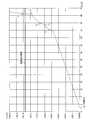
- FIG. 3 is a diagram illustrating an impurity concentration peak (P x ) between A1 and A2 and a boundary (V y ) between the impurity concentration peaks in the first embodiment.
- the peak Px is the maximum value of the impurity concentration.
- the position of the peak P x and the height of the impurity concentration can be set by the acceleration voltage and impurity concentration of the impurity to be doped.
- the boundary V y is the minimum value of the impurity concentration between the two peaks P x .
- the vertical axis represents the impurity concentration [/ cm 3 ] and represents the net impurity concentration (net doping) of the first conductivity type and the second conductivity type.
- FIG. 3 corresponds to the impurity concentration at A1-A2 in FIG.
- the horizontal axis indicates the position of the semiconductor substrate 10 in the first direction.
- the front surface 19 is set to a position 0 [ ⁇ m]
- the second surface 16 is set to a position 110 [ ⁇ m].
- the first surface 14 in the drift layer 12 is located between the position 0 [ ⁇ m] and the position 10 [ ⁇ m].
- This example is a doping pattern having an impurity concentration in the IGBT 100 having a withstand voltage of 1,200V.
- A1-A2 is a region along the first direction from the front surface 19 to the second surface 16.
- the first impurity concentration peak closest to the first surface 14 among the plurality of impurity concentration peaks is referred to as a first peak P1.
- the second closest to the first surface 14 is referred to as a second peak P 2
- the third closest to the first surface 14 is referred to as a third peak P 3
- the fourth closest to the first surface 14 is referred to as a fourth peak P 4.
- the peaks P1 to P3 are proton (H + ) peaks.
- the fourth peak P 4 on the second surface 16 side than the third peak P 3 is a peak other than protons.
- a boundary V 1 is present between the peaks P 1 and P 2 .
- a boundary V 2 between the peaks P 2 and P 3 , a boundary V 3 between the peaks P 3 and P 4, and a boundary V 4 between the peaks P 4 and P 5.
- first to fourth doped pattern in ascending order impurity concentration at the peak P 3, referred to as first to fourth doped pattern. Note that the integral concentration described later is lower in the order of the first to fourth dope patterns.
- the impurity concentration of the peak P 3 is different in the first to fourth doped pattern, the position of the peak P 3 are the same in the first to fourth doped pattern.
- FIG. 3 is a diagram showing four different dope patterns in one graph. Different types of doping patterns correspond to different IGBTs 100.
- One IGBT 100 as a finished product has one kind of dope pattern.
- the total dose amount of the first dope pattern is 1, the total dose amount of the second dope pattern is 1.4, and the total dose amount of the third dope pattern is 2.6.
- the total dose amount of the fourth dope pattern is 4.5. The difference in the total dose amount is particularly remarkable in the vicinity of the third peak and the third boundary.
- the four different first to fourth doping patterns include the third peaks P 3-1 , P 3-2 , P 3-3 and P 3-4 , and the third boundaries V 3-1 , V 3 It has different impurity concentrations in the vicinity of 3-2 , V3-3 and V3-4 .
- the four different dope patterns in the other regions match. For example, in the region from position 0 [ ⁇ m] to position 100 [ ⁇ m], four different types of dope patterns match. For example, also in P 4 , V 4, and P 5 , the first to fourth dope patterns match.
- the impurity concentration increases in the order of P 3-1 , P 3-2 , P 3-3 and P 3-4 , and the third boundary is V 3-1 , V 3-2 , V 3
- the impurity concentration increases in the order of 3-3 and V 3-4 .
- FIG. 4 is an enlarged view showing a position from 80 [ ⁇ m] to 110 [ ⁇ m] in FIG. As can be seen from FIG. 4, the four different dope patterns are completely identical in the range other than the second boundary V 2 to the fourth peak P 4 .
- the maximum value of the impurity concentration smaller than the third peak P 3-1 and the minimum impurity concentration are set. Values are observed.
- the minimum value and the maximum value of the impurity concentration between the second boundary V 2 and the third peak P 3-1 are not intentionally formed by the acceleration voltage and impurity concentration of the impurity to be doped. Therefore, these are not peaks P and boundaries V in this document.
- the position of the peak P 1 is the larger 97 [[mu] m] smaller range than 94 [ ⁇ m].
- the position of the peak P 2 is the larger 100 [[mu] m] smaller range than 97 [ ⁇ m].
- the position of the peak P 3 is in a large 108 [[mu] m] smaller range than 105 [ ⁇ m].
- the position of the peak P 4 are in large 110 [[mu] m] smaller range than 108 [ ⁇ m].
- the above range can be rephrased as follows.
- the ratio from the position of 0 [ ⁇ m] to the position of the peak P 1 with respect to the substrate length L is in a range greater than 85% and less than 89%. Further, the ratio from the position of 0 [ ⁇ m] to the position of the peak P 2 with respect to the substrate length L is in a range larger than 89% and smaller than 91%. Further, the ratio from the position of 0 [ ⁇ m] to the position of the peak P 3 with respect to the substrate length L is in a range larger than 96% and smaller than 98%. In addition, the ratio from the position of 0 [ ⁇ m] to the position of the peak P 4 with respect to the substrate length L is in a range larger than 98% and smaller than 100%.
- FIG. 5 is a diagram showing the relationship between the impurity concentration peak (P x ) between A1 and A2 and the critical integral concentration in the first embodiment.
- the vertical axis represents the integrated concentration [/ cm 2 ], and the horizontal axis represents the position of the semiconductor substrate 10 in the first direction, as in FIGS.
- the graph near 110 [ ⁇ m] is omitted because of the scale.
- the value obtained by integrating the impurity concentration along the first direction from the first surface 14, which is the junction interface between the drift layer 12 and the base layer 18, to a specific position of the drift layer 12 is expressed as an integrated concentration. Called. Further, in the present specification, a forward bias is applied between the collector electrode 54 and the emitter electrode 52, the maximum value of the electric field intensity reaches the critical electric field intensity, and avalanche breakdown occurs. When the drift layer 12 is depleted up to a specific position in the first direction, the integrated value of the impurity concentration at the specific position is referred to as reaching a critical integral concentration. In the IGBT 100, applying a forward bias between the collector electrode 54 and the emitter electrode 52 means that the potential of the collector electrode 54 is higher than the potential of the emitter electrode 52.
- the position of the critical integrated concentration in the drift layer 12 can be adjusted by adjusting the peak positions (peaks P 1 to P 3 ) of the FS layer 22 in the four dope patterns.
- the critical integral concentration may be located between 1.2E12 [/ cm 2 ] and 2.0E12 [/ cm 2 ].
- the critical integral concentration in this example is about 1.4E12 [/ cm 2 ].
- the integrated concentration from the first surface 14 in the first direction to the boundary V 1 is not more than the critical integrated concentration. Further, in the first to fourth doped pattern, from the first surface 14 in the first direction, the integration density to the boundary V 2, is below the critical integration density.
- the integrated concentration from the first surface 14 to the boundary V 3-1 in the first direction is not more than the critical integrated concentration.
- the integrated concentration from the first surface 14 to the boundary V 3-2 in the first direction is not more than the critical integrated concentration.
- the integrated concentration from the first surface 14 in the first direction to the boundary V 3 exceeds the critical integrated concentration.
- the integrated concentration from the first surface 14 in the first direction to the peak P 3-2 is equal to or lower than the critical integrated concentration.
- FIG. 6 is an enlarged view showing the position from the position 80 [ ⁇ m] to the position 110 [ ⁇ m] in FIG. 5.
- the FS layer 22 is formed by three peaks of the peaks P 1 , P 2 and P 3 . Since the critical integral concentration is not reached at the first peak P 1 of the FS layer 22, the FS layer 22 can be provided at a relatively high concentration near the emitter electrode 52. Thereby, the oscillation at the time of switching can be suppressed. In this example, since the critical integrated concentration is reached in the FS layer 22 or the buffer layer 24, the extension of the depletion layer in the FS layer 22 or the buffer layer 24 can be suppressed.
- the buffer layer 24 (peak P 4 ) having a higher concentration than the FS layer 22 and the collector layer 26 (peak P 5 ) having a higher concentration than the buffer layer 24 are further provided.
- the impurity concentration of the FS layer 22 is 1.0E14 to 1.0E16
- the impurity concentration of the peak P 4 is 1.0E16 to 1.0E17
- the impurity concentration of the peak P 5 is 1.0E17 to 1 .0E18.
- the peak P 4 and peak P 5 is not shown in FIG.
- the carrier injection characteristics can be controlled by the buffer layer 24 and the collector layer 26.
- the hole injection characteristics into the drift layer 12 can be improved by the collector layer 26.
- collector voltage Vcc 680 [V]
- gate-on resistance Rgon 4.1 [ ⁇ ]
- gate-off resistance Rgoff 20 [ ⁇ ]
- gate input pulse time 2 [ ⁇ s]
- chip junction temperature Tj 25 [ C.]
- the gate-emitter potential Vge was gradually increased from 15 [V]
- the collector voltage Vcc is a voltage applied to the collector terminal 53.
- the gate-emitter potential Vge is a potential difference between the gate terminal 50 and the emitter terminal 51.
- the collector-emitter current Ic is a current that flows between the collector terminal 53 and the emitter terminal 51.
- collector voltage Vcc 870 [V]
- collector-emitter current Ice 300 [A / cm 2 ]
- gate-on resistance Rgon 1 [ ⁇ ]
- gate-off resistance Rgoff 1 [ ⁇ ]
- floating inductance Ls 70 [nH]
- chip junction temperature Tj 25 [° C.]
- the gate-emitter potential Vge was turned off from 15 [V] to 0 [V]
- the gate-emitter potential Vge was turned off from 15 [V] to 0 [V]
- chip junction temperature Tj 25 [° C.]
- the gate-emitter potential Vge was turned off from 15 [V] to 0 [V]
- chip junction temperature Tj 25 [° C.]
- the gate-emitter potential Vge was turned off from 15 [V] to 0 [V]
- chip junction temperature Tj 25 [° C.
- the gate-emitter potential Vge was turned off from 15 [V] to
- FIG. 7 is a diagram illustrating an impurity concentration peak (P x ) between A1 and A2 and a boundary (V y ) between impurity concentration peaks in the second embodiment.
- the vertical axis and the horizontal axis are the same as those in FIG.
- the second surface 16 corresponds to the position 70 [ ⁇ m].
- the drift layer 12 is thinner than the first embodiment, and has a withstand voltage of 600V.
- the position of the peak P x is different from that of the first embodiment.
- Other points may be the same as in the first embodiment.
- This example shows one kind of dope pattern.
- FIG. 8 is an enlarged view showing the position 40 [ ⁇ m] to the position 70 [ ⁇ m] in FIG. 6.
- the position of the peak P 1 is the larger 57 [[mu] m] smaller range than 54 [ ⁇ m].
- the position of the peak P 2 is the larger 60 [[mu] m] smaller range than 57 [ ⁇ m].
- the position of the peak P 3 is in a large 68 [[mu] m] smaller range than 65 [ ⁇ m].
- the position of the peak P 4 is largely 70 [[mu] m] smaller range than 68 [ ⁇ m].
- the above range can be rephrased as follows.
- the ratio from the position of 0 [ ⁇ m] to the position of the peak P 1 with respect to the substrate length L is in a range larger than 77% and smaller than 81%.
- the ratio from the position of 0 [ ⁇ m] to the position of the peak P 2 with respect to the substrate length L is in a range larger than 81% and smaller than 86%.
- the ratio from the position of 0 [ ⁇ m] to the position of the peak P 3 with respect to the substrate length L is in a range larger than 93% and smaller than 97%.
- the ratio from the position of 0 [ ⁇ m] to the position of the peak P 4 with respect to the substrate length L is in a range larger than 97% and smaller than 100%.
- FIG. 9 is a diagram showing the relationship between the impurity concentration peak (P x ) between A1 and A2 and the critical integral concentration in the second embodiment.
- the integration density of the first surface 14 in the first direction to the boundary V 1 was, is below the critical integration density.
- the integration density of the first surface 14 in the first direction to the peak P 2 is below the critical integration density.
- the integration density of the first surface 14 in the first direction to the border V 2 is also below the critical integration density.
- the integration density of the first surface 14 in the first direction to a peak P 3 is greater than the critical integration density.
- the manufacturing process of the IGBT 100 in the second embodiment is basically the same as that in the first embodiment. The differences are listed below.
- the semiconductor substrate 10 in the second embodiment may have a thickness of less than 100 [ ⁇ m] and a specific resistance of less than 50 [ ⁇ cm].
- the semiconductor substrate 10 of this example has a thickness of 70 [ ⁇ m] and a specific resistance of 30 [ ⁇ cm].
- protons are doped with a dose of 1.0E14 cm ⁇ 2 and an acceleration voltage of 0.40 MeV in order to form a third peak at a position 4.2 ⁇ m away from the second surface 16.
- Other points are the same as in the first embodiment. Also in this example, the same effect as the first embodiment can be obtained.
- collector voltage Vcc 360 [V]
- gate on resistance Rgon 1 [ ⁇ ]
- gate off resistance Rgoff 90 [ ⁇ ]
- gate input pulse time 2 [ ⁇ s]
- chip junction temperature Tj ⁇ 40 [° C.
- the gate-emitter potential Vge was gradually increased from 15 [V], and a large current short-circuit withstand test was conducted.
- collector voltage Vcc 410 [V]
- collector-emitter current Ice 310 [A / cm 2 ]
- gate-on resistance Rgon 3.9 [ ⁇ ]
- gate-off resistance Rgoff 3.9 [ ⁇
- the floating inductance Ls 70 [nH]
- the chip junction temperature Tj 175 [° C.]
- the gate-emitter potential Vge was turned off from 15 [V] to 0 [V]
- the turn-off surge test was performed.
- the peak of the collector-emitter voltage Vce at the time of turn-off is about 700 [V].
- the surge voltage at turn-off is lower than before.
- turn-off vibration was also suppressed compared to the conventional one.
- the collector voltage Vcc 350 [V]
- the collector-emitter current Ice 490 [A / cm 2 ]
- the other conditions are the same as the above-described turn-off surge test, and the turn-off surge test is performed. It was.
- the peak of the collector-emitter voltage Vce at the time of turn-off of the IGBT 100 of this example is about 750 [V].
- the surge voltage at turn-off is lower than before.
- turn-off vibration was also suppressed compared to the conventional one.
- Figure 10 is a diagram showing the relationship between the critical field strength E c, and the critical integration density n c to the donor concentration.
- the horizontal axis is the donor concentration (n-type impurity concentration) [/ cm 3 ]
- the left vertical axis is the critical electric field intensity E c [V / cm]
- the right vertical axis is the critical integral concentration n c [/ cm 2 ].
- the critical electric field strength E c and the critical integrated concentration n c have a corresponding relationship with respect to the donor concentration.
- the n-type layer corresponds to the drift layer 12 and the p-type layer corresponds to the base layer 18. Further, applying a reverse bias voltage to the pn junction corresponds to applying a forward bias to the IGBT 100 in which the potential of the collector electrode 54 is higher than the potential of the emitter electrode 52.
- the value of the electric field strength at which avalanche breakdown occurs is called the critical electric field strength (Critical Electric Field Strength).
- Avalanche breakdown depends on the constituent elements of the semiconductor, the impurities doped in the semiconductor, and the concentration of the impurities. Assuming that the donor concentration is N D and the critical electric field strength is E C , the critical electric field strength E C is expressed by Equation 1 when ionization integration is performed using the impact ionization coefficient in silicon (Si).
- Equation 1 As it can be seen from Equation 1, once the donor concentration N D, the critical field strength E C is determined. Poisson's formula is expressed by Formula 2 when only the one-dimensional direction (x direction) is considered.
- Equation 3 is obtained by integrating Equation 2 with a depth x.
- Equation 3 The position of the end portion of the depletion layer at the position opposite to x 0 and the pn junction the position of the pn junction at the origin 0, n-type layer.
- Equation 4 is expressed by Equation 5.
- Equation 5 is a constant on both sides.
- Equation 6 shows the correspondence between the critical integral concentration n c and the critical electric field strength E c .
- the critical integration density n c is formed with the constant corresponding to the critical field strength E c.
- the donor concentration N D is the density distribution in the x direction of the n-type layer is assumed to be uniform. Since the critical electric field strength E c depends on the n-type layer donor concentration N D (see Formula 5), the critical integrated concentration n c also depends on the n-type layer donor concentration N D. In the range of the donor concentration N D is 1 ⁇ 10 13 ⁇ 1 ⁇ 10 15 (/ cm 3), the critical integration density n c becomes 1.1 ⁇ 10 12 ⁇ 2.0 ⁇ 10 12 (/ cm 2). Given that the donor concentration is the concentration range over several orders of magnitude, can be regarded as critical integration density n c is substantially constant.
- the critical integrated from Equation 6 concentration n c can be evaluated approximately 1.4 ⁇ 10 12 (/ cm 2 ).
- the critical integration density n from Equation 6 c can be evaluated as about 1.55 ⁇ 10 12 (/ cm 2 ).
- the FS layer 22 by adjusting the position of the peak P x, to adjust the position of the critical integration density n c. Since the FS layer 22 reaches a critical integral density n c, it can be provided at relatively high concentrations in relatively emitter electrode 52 toward the FS layer 22. Thereby, the oscillation at the time of switching can be suppressed. In addition, leakage current can be suppressed and RBSOA can be improved. Furthermore, by controlling the hole injection characteristics with the collector layer 26 having an impurity concentration higher than that of the FS layer 22, the critical electric field strength E c at the position of the critical integral concentration n c can be suppressed.
- the high-current short-circuit withstand capability can be improved without bringing the FS layer 22 closer to the collector electrode 54 than before and without lowering the concentration of the FS layer 22 than before.
- the breakdown voltage can be improved. In this way, it is possible to achieve both the improvement of the large current short-circuit resistance and the suppression of oscillation during switching.
- donor concentration N D of the drift layer 12 is not a uniform inside FS layer 22.
- the critical integration density n c are the integral amount in the first direction a depletion layer spreads, increase or decrease of the impurity concentration in the FS layer 22 is absorbed by the integrated amount.
- critical total impurities is not limited to silicon but can be applied to wide band gap semiconductors such as silicon carbide (SiC), gallium nitride (GaN), diamond, and gallium oxide (Ga 2 O 3 ). is there. That is, the value of each substance may be used for the impact ionization coefficient in order to derive Formula 1 and for the relative dielectric constant in Formula 2.
Landscapes
- Thin Film Transistor (AREA)
- Metal-Oxide And Bipolar Metal-Oxide Semiconductor Integrated Circuits (AREA)
- Thyristors (AREA)
- Bipolar Transistors (AREA)
Abstract
Description
[先行技術文献]
[特許文献]
[特許文献1] 特表2010-541266号公報
[特許文献2] 特開2014-99643号公報
第2番目の不純物濃度ピークの位置は、おもて面から57μmより大きく、60μmより小さい範囲にあってよい。
第3番目の不純物濃度ピークの位置は、おもて面から65μmより大きく、68μmより小さい範囲にあってよい。
プロトン以外の不純物濃度ピークの位置は、おもて面から68μmより大きく、70μmより小さい範囲にあってよい。


Claims (12)
- 第1の面と前記第1の面の反対側に位置する第2の面とを有する第1導電型の半導体層と、
前記第1導電型の半導体層の前記第1の面に接して設けられた第2導電型の半導体層と
を備え、
前記第1導電型の半導体層は、前記第1の面から前記第2の面への第1方向の異なる位置において、複数の不純物濃度ピークを有し、
前記第1方向における前記第1導電型の半導体層と前記第2導電型の半導体層との接合界面である前記第1の面から、前記複数の不純物濃度ピークのうち前記第1の面に1番目に近い第1番目の不純物濃度ピークと、前記第1の面に2番目に近い第2番目の不純物濃度ピークとの境界までにおける積分濃度が、臨界積分濃度以下である、半導体装置。 - 前記第1方向における前記第1の面から、前記第2番目の不純物濃度ピークと、前記複数の不純物濃度ピークのうち前記第1の面に3番目に近い第3番目の不純物濃度ピークとの境界までの積分濃度が、前記臨界積分濃度以下である、
請求項1に記載の半導体装置。 - 前記第1導電型の半導体層は、前記複数の不純物濃度ピークのうち前記第3番目の不純物濃度ピークよりも前記第2の面側に、プロトン以外の不純物濃度ピークを有する
請求項2に記載の半導体装置。 - 前記第1方向における前記第1の面から、前記第3番目の不純物濃度ピークと、前記プロトン以外の不純物濃度ピークとの境界までの積分濃度が、前記臨界積分濃度以下である
請求項3に記載の半導体装置。 - 前記第1方向における前記第1の面から、前記第3番目の不純物濃度ピークまでの積分濃度が、前記臨界積分濃度以下である
請求項3に記載の半導体装置。 - 前記第1導電型の半導体層は、前記第2の面と、前記プロトン以外の不純物の濃度ピークとの間に、前記プロトン以外の不純物の濃度ピークよりも高い不純物濃度の第2導電型の不純物濃度ピークを有する
請求項3に記載の半導体装置。 - 前記第1導電型の半導体層および前記第2導電型の半導体層の前記第1方向における長さに対する前記第2導電型の半導体層の前記接合界面とは反対側に位置するおもて面から、前記第1番目の不純物濃度ピークの位置までの割合は、85%より大きく、89%より小さい範囲であり、
前記第1導電型の半導体層および前記第2導電型の半導体層の前記第1方向における長さに対する前記おもて面から、前記第2番目の不純物濃度ピークの位置までの割合は、89%より大きく、91%より小さい範囲であり、
前記第1導電型の半導体層および前記第2導電型の半導体層の前記第1方向における長さに対する前記おもて面から、前記第3番目の不純物濃度ピークの位置までの割合は、96%より大きく、98%より小さい範囲であり、
前記第1導電型の半導体層および前記第2導電型の半導体層の前記第1方向における長さに対する前記おもて面から、前記プロトン以外の不純物濃度ピークの位置までの割合は、98%より大きく、100%より小さい範囲である
請求項3に記載の半導体装置。 - 前記第1番目の不純物濃度ピークの位置は、前記第2導電型の半導体層の前記接合界面とは反対側に位置するおもて面から94μmより大きく、97μmより小さい範囲にあり、
前記第2番目の不純物濃度ピークの位置は、前記おもて面から97μmより大きく、100μmより小さい範囲にあり、
前記第3番目の不純物濃度ピークの位置は、前記おもて面から105μmより大きく、108μmより小さい範囲にあり、
前記プロトン以外の不純物濃度ピークの位置は、前記おもて面から108μmより大きく、110μmより小さい範囲にある
請求項3に記載の半導体装置。 - 前記第1導電型の半導体層および前記第2導電型の半導体層の前記第1方向における長さに対する前記第2導電型の半導体層の前記接合界面とは反対側に位置するおもて面から、前記第1番目の不純物濃度ピークの位置までの割合は、77%より大きく、81%より小さい範囲であり、
前記第1導電型の半導体層および前記第2導電型の半導体層の前記第1方向における長さに対する前記おもて面から前記第2番目の不純物濃度ピークの位置までの割合は、81%より大きく、86%より小さい範囲であり、
前記第1導電型の半導体層および前記第2導電型の半導体層の前記第1方向における長さに対する前記おもて面から前記第3番目の不純物濃度ピークの位置までの割合は、93%より大きく、97%より小さい範囲であり、
前記第1導電型の半導体層および前記第2導電型の半導体層の前記第1方向における長さに対する前記おもて面から前記プロトン以外の不純物濃度ピークの位置までの割合は、97%より大きく、100%より小さい範囲である、
請求項3に記載の半導体装置。 - 前記第1番目の不純物濃度ピークの位置は、前記第2導電型の半導体層の前記接合界面とは反対側に位置するおもて面から54μmより大きく、57μmより小さい範囲にあり、
前記第2番目の不純物濃度ピークの位置は、前記おもて面から57μmより大きく、60μmより小さい範囲にあり、
前記第3番目の不純物濃度ピークの位置は、前記おもて面から65μmより大きく、68μmより小さい範囲にあり、
前記プロトン以外の不純物濃度ピークの位置は、前記おもて面から68μmより大きく、70μmより小さい範囲にある、
請求項3に記載の半導体装置。 - 少なくとも前記第2導電型の半導体層の一部において、トレンチ状に設けられたゲート絶縁膜と、
前記ゲート絶縁膜に接して設けられたゲート電極と
をさらに有する、請求項1に記載の半導体装置。 - 前記第1番目から第3番目の不純物濃度ピークは、水素、空孔及び酸素による複合ドナーを含むことを特徴とする請求項1に記載の半導体装置。
Priority Applications (5)
| Application Number | Priority Date | Filing Date | Title |
|---|---|---|---|
| CN201680003832.6A CN107004716B (zh) | 2015-06-17 | 2016-06-13 | 半导体装置 |
| CN202011371539.XA CN112490281B (zh) | 2015-06-17 | 2016-06-13 | 半导体装置 |
| DE112016000168.1T DE112016000168B4 (de) | 2015-06-17 | 2016-06-13 | Halbleitervorrichtung |
| JP2017525230A JP6292349B2 (ja) | 2015-06-17 | 2016-06-13 | 半導体装置 |
| US15/607,697 US10229972B2 (en) | 2015-06-17 | 2017-05-30 | Semiconductor device |
Applications Claiming Priority (2)
| Application Number | Priority Date | Filing Date | Title |
|---|---|---|---|
| JP2015122037 | 2015-06-17 | ||
| JP2015-122037 | 2015-06-17 |
Related Child Applications (1)
| Application Number | Title | Priority Date | Filing Date |
|---|---|---|---|
| US15/607,697 Continuation US10229972B2 (en) | 2015-06-17 | 2017-05-30 | Semiconductor device |
Publications (1)
| Publication Number | Publication Date |
|---|---|
| WO2016204126A1 true WO2016204126A1 (ja) | 2016-12-22 |
Family
ID=57545874
Family Applications (1)
| Application Number | Title | Priority Date | Filing Date |
|---|---|---|---|
| PCT/JP2016/067597 Ceased WO2016204126A1 (ja) | 2015-06-17 | 2016-06-13 | 半導体装置 |
Country Status (5)
| Country | Link |
|---|---|
| US (1) | US10229972B2 (ja) |
| JP (3) | JP6292349B2 (ja) |
| CN (2) | CN107004716B (ja) |
| DE (1) | DE112016000168B4 (ja) |
| WO (1) | WO2016204126A1 (ja) |
Cited By (15)
| Publication number | Priority date | Publication date | Assignee | Title |
|---|---|---|---|---|
| CN108242464A (zh) * | 2016-12-27 | 2018-07-03 | 三菱电机株式会社 | 半导体装置、电力转换装置及半导体装置的制造方法 |
| WO2018135448A1 (ja) * | 2017-01-17 | 2018-07-26 | 富士電機株式会社 | 半導体装置 |
| JP2020043301A (ja) * | 2018-09-13 | 2020-03-19 | 株式会社デンソー | 半導体装置 |
| JP2020074495A (ja) * | 2020-02-17 | 2020-05-14 | ローム株式会社 | SiC半導体装置 |
| JP2020202321A (ja) * | 2019-06-12 | 2020-12-17 | サンケン電気株式会社 | 半導体装置 |
| WO2021075330A1 (ja) * | 2019-10-17 | 2021-04-22 | 富士電機株式会社 | 半導体装置および半導体装置の製造方法 |
| JP2022035157A (ja) * | 2020-08-20 | 2022-03-04 | 三菱電機株式会社 | 半導体装置および半導体装置の製造方法 |
| DE112021000082T5 (de) | 2020-03-04 | 2022-04-21 | Fuji Electric Co., Ltd. | Halbleitervorrichtung, verfahren zur herstellung einer halbleitervorrichtung und leistungsumwandlungsvorrichtung mit einer halbleitervorrichtung |
| US11545564B2 (en) | 2020-08-20 | 2023-01-03 | Mitsubishi Electric Corporation | Semiconductor device |
| WO2023042886A1 (ja) * | 2021-09-15 | 2023-03-23 | 富士電機株式会社 | 半導体装置および半導体装置の製造方法 |
| US11621319B2 (en) | 2018-08-10 | 2023-04-04 | Rohm Co., Ltd. | SiC semiconductor device |
| WO2024090117A1 (ja) * | 2022-10-27 | 2024-05-02 | 株式会社デンソー | 半導体装置 |
| US12191358B2 (en) | 2019-08-09 | 2025-01-07 | Fuji Electric Co., Ltd. | Semiconductor device |
| US12543355B2 (en) | 2020-11-17 | 2026-02-03 | Fuji Electric Co., Ltd. | Semiconductor device |
| US12615811B2 (en) | 2022-02-17 | 2026-04-28 | Fuji Electric Co., Ltd. | Semiconductor device to suppress leakage current |
Families Citing this family (12)
| Publication number | Priority date | Publication date | Assignee | Title |
|---|---|---|---|---|
| JP6237921B2 (ja) * | 2014-09-30 | 2017-11-29 | 富士電機株式会社 | 半導体装置および半導体装置の製造方法 |
| DE102017126853B4 (de) * | 2017-11-15 | 2019-11-21 | Infineon Technologies Dresden Gmbh | Halbleitervorrichtung mit Puffergebiet |
| JP6664446B2 (ja) * | 2018-08-10 | 2020-03-13 | ローム株式会社 | SiC半導体装置 |
| JP6964566B2 (ja) * | 2018-08-17 | 2021-11-10 | 三菱電機株式会社 | 半導体装置およびその製造方法 |
| JP6993946B2 (ja) * | 2018-08-21 | 2022-01-14 | 株式会社東芝 | 半導体素子 |
| DE102018132236B4 (de) | 2018-12-14 | 2023-04-27 | Infineon Technologies Ag | Leistungshalbleiterbauelement und Verfahren zu dessen Herstellung |
| CN113471273A (zh) * | 2020-03-31 | 2021-10-01 | 比亚迪半导体股份有限公司 | 绝缘栅双极型晶体管及制备方法、电子设备 |
| DE112021000205T5 (de) * | 2020-07-15 | 2022-08-18 | Fuji Electric Co., Ltd. | Halbleitervorrichtung |
| JP7415913B2 (ja) * | 2020-12-28 | 2024-01-17 | 三菱電機株式会社 | 半導体装置及びその製造方法 |
| CN116978937A (zh) * | 2021-02-07 | 2023-10-31 | 华为技术有限公司 | 半导体器件及相关模块、电路、制备方法 |
| CN116569307A (zh) * | 2021-06-17 | 2023-08-08 | 富士电机株式会社 | 半导体装置以及制造半导体装置的方法 |
| CN113644123B (zh) * | 2021-06-28 | 2024-09-06 | 华为技术有限公司 | 半导体器件及相关芯片和制备方法 |
Citations (1)
| Publication number | Priority date | Publication date | Assignee | Title |
|---|---|---|---|---|
| WO2011052787A1 (ja) * | 2009-11-02 | 2011-05-05 | 富士電機システムズ株式会社 | 半導体装置および半導体装置の製造方法 |
Family Cites Families (15)
| Publication number | Priority date | Publication date | Assignee | Title |
|---|---|---|---|---|
| US6482681B1 (en) * | 2000-05-05 | 2002-11-19 | International Rectifier Corporation | Hydrogen implant for buffer zone of punch-through non epi IGBT |
| JP4093042B2 (ja) * | 2002-12-09 | 2008-05-28 | 富士電機デバイステクノロジー株式会社 | 半導体装置 |
| JP2006049473A (ja) * | 2004-08-03 | 2006-02-16 | Toyota Central Res & Dev Lab Inc | 縦型半導体装置 |
| DE102004047749B4 (de) * | 2004-09-30 | 2008-12-04 | Infineon Technologies Austria Ag | Halbleiterbauteil Diode und IGBT sowie dafür geeignetes Herstellungsverfahren |
| US7538412B2 (en) * | 2006-06-30 | 2009-05-26 | Infineon Technologies Austria Ag | Semiconductor device with a field stop zone |
| US7989888B2 (en) * | 2006-08-31 | 2011-08-02 | Infineon Technologies Autria AG | Semiconductor device with a field stop zone and process of producing the same |
| EP2045844A1 (en) | 2007-10-03 | 2009-04-08 | ABB Technology AG | Semiconductor Module |
| US7960222B1 (en) * | 2007-11-21 | 2011-06-14 | National Semiconductor Corporation | System and method for manufacturing double EPI N-type lateral diffusion metal oxide semiconductor transistors |
| JP5365009B2 (ja) | 2008-01-23 | 2013-12-11 | 富士電機株式会社 | 半導体装置およびその製造方法 |
| JP6006918B2 (ja) * | 2011-06-06 | 2016-10-12 | ルネサスエレクトロニクス株式会社 | 半導体装置、半導体装置の製造方法、及び電子装置 |
| JP5733417B2 (ja) * | 2011-11-15 | 2015-06-10 | 富士電機株式会社 | 半導体装置および半導体装置の製造方法 |
| JP5817686B2 (ja) * | 2011-11-30 | 2015-11-18 | 株式会社デンソー | 半導体装置 |
| WO2013089256A1 (ja) * | 2011-12-15 | 2013-06-20 | 富士電機株式会社 | 半導体装置および半導体装置の製造方法 |
| EP2790209B1 (en) * | 2012-03-30 | 2019-09-25 | Fuji Electric Co., Ltd. | Manufacturing method for semiconductor device |
| KR102070959B1 (ko) * | 2012-04-24 | 2020-01-30 | 온세미컨덕터코리아 주식회사 | 파워 소자 및 그 제조방법 |
-
2016
- 2016-06-13 CN CN201680003832.6A patent/CN107004716B/zh active Active
- 2016-06-13 CN CN202011371539.XA patent/CN112490281B/zh active Active
- 2016-06-13 JP JP2017525230A patent/JP6292349B2/ja active Active
- 2016-06-13 WO PCT/JP2016/067597 patent/WO2016204126A1/ja not_active Ceased
- 2016-06-13 DE DE112016000168.1T patent/DE112016000168B4/de active Active
-
2017
- 2017-05-30 US US15/607,697 patent/US10229972B2/en active Active
- 2017-12-19 JP JP2017242421A patent/JP6562066B2/ja active Active
-
2019
- 2019-01-30 JP JP2019014714A patent/JP6725015B2/ja active Active
Patent Citations (1)
| Publication number | Priority date | Publication date | Assignee | Title |
|---|---|---|---|---|
| WO2011052787A1 (ja) * | 2009-11-02 | 2011-05-05 | 富士電機システムズ株式会社 | 半導体装置および半導体装置の製造方法 |
Cited By (37)
| Publication number | Priority date | Publication date | Assignee | Title |
|---|---|---|---|---|
| JP2018107303A (ja) * | 2016-12-27 | 2018-07-05 | 三菱電機株式会社 | 半導体装置、電力変換装置および半導体装置の製造方法 |
| CN108242464A (zh) * | 2016-12-27 | 2018-07-03 | 三菱电机株式会社 | 半导体装置、电力转换装置及半导体装置的制造方法 |
| US11984482B2 (en) | 2017-01-17 | 2024-05-14 | Fuji Electric Co., Ltd. | Semiconductor device |
| WO2018135448A1 (ja) * | 2017-01-17 | 2018-07-26 | 富士電機株式会社 | 半導体装置 |
| JPWO2018135448A1 (ja) * | 2017-01-17 | 2019-06-27 | 富士電機株式会社 | 半導体装置 |
| US10825904B2 (en) | 2017-01-17 | 2020-11-03 | Fuji Electric Co., Ltd. | Semiconductor device |
| US12317560B2 (en) | 2017-01-17 | 2025-05-27 | Fuji Electric Co., Ltd. | Semiconductor device |
| US11621319B2 (en) | 2018-08-10 | 2023-04-04 | Rohm Co., Ltd. | SiC semiconductor device |
| US12255227B2 (en) | 2018-08-10 | 2025-03-18 | Rohm Co., Ltd. | SiC semiconductor device |
| JP7010184B2 (ja) | 2018-09-13 | 2022-01-26 | 株式会社デンソー | 半導体装置 |
| WO2020054446A1 (ja) * | 2018-09-13 | 2020-03-19 | 株式会社デンソー | 半導体装置 |
| JP2020043301A (ja) * | 2018-09-13 | 2020-03-19 | 株式会社デンソー | 半導体装置 |
| CN112689902A (zh) * | 2018-09-13 | 2021-04-20 | 株式会社电装 | 半导体装置 |
| JP2020202321A (ja) * | 2019-06-12 | 2020-12-17 | サンケン電気株式会社 | 半導体装置 |
| JP7375340B2 (ja) | 2019-06-12 | 2023-11-08 | サンケン電気株式会社 | 半導体装置 |
| US12191358B2 (en) | 2019-08-09 | 2025-01-07 | Fuji Electric Co., Ltd. | Semiconductor device |
| WO2021075330A1 (ja) * | 2019-10-17 | 2021-04-22 | 富士電機株式会社 | 半導体装置および半導体装置の製造方法 |
| US12369370B2 (en) | 2019-10-17 | 2025-07-22 | Fuji Electric Co., Ltd. | Semiconductor device and manufacturing method for semiconductor device |
| JP7272454B2 (ja) | 2019-10-17 | 2023-05-12 | 富士電機株式会社 | 半導体装置および半導体装置の製造方法 |
| US11894426B2 (en) | 2019-10-17 | 2024-02-06 | Fuji Electric Co., Ltd. | Semiconductor device and manufacturing method for semiconductor device |
| JPWO2021075330A1 (ja) * | 2019-10-17 | 2021-04-22 | ||
| JP7129437B2 (ja) | 2020-02-17 | 2022-09-01 | ローム株式会社 | SiC半導体装置 |
| JP2020074495A (ja) * | 2020-02-17 | 2020-05-14 | ローム株式会社 | SiC半導体装置 |
| DE112021000082T5 (de) | 2020-03-04 | 2022-04-21 | Fuji Electric Co., Ltd. | Halbleitervorrichtung, verfahren zur herstellung einer halbleitervorrichtung und leistungsumwandlungsvorrichtung mit einer halbleitervorrichtung |
| US12266719B2 (en) | 2020-03-04 | 2025-04-01 | Fuji Electric Co., Ltd. | Semiconductor device, manufacturing method of semiconductor device, and power conversion device comprising semiconductor device |
| JP7528628B2 (ja) | 2020-08-20 | 2024-08-06 | 三菱電機株式会社 | 半導体装置および半導体装置の製造方法 |
| DE102021119689B4 (de) | 2020-08-20 | 2024-01-04 | Mitsubishi Electric Corporation | Halbleitervorrichtung |
| US11545564B2 (en) | 2020-08-20 | 2023-01-03 | Mitsubishi Electric Corporation | Semiconductor device |
| JP2022035157A (ja) * | 2020-08-20 | 2022-03-04 | 三菱電機株式会社 | 半導体装置および半導体装置の製造方法 |
| US12543355B2 (en) | 2020-11-17 | 2026-02-03 | Fuji Electric Co., Ltd. | Semiconductor device |
| JP7597233B2 (ja) | 2021-09-15 | 2024-12-10 | 富士電機株式会社 | 半導体装置および半導体装置の製造方法 |
| JPWO2023042886A1 (ja) * | 2021-09-15 | 2023-03-23 | ||
| WO2023042886A1 (ja) * | 2021-09-15 | 2023-03-23 | 富士電機株式会社 | 半導体装置および半導体装置の製造方法 |
| US12615811B2 (en) | 2022-02-17 | 2026-04-28 | Fuji Electric Co., Ltd. | Semiconductor device to suppress leakage current |
| JP2024064037A (ja) * | 2022-10-27 | 2024-05-14 | 株式会社デンソー | 半導体装置 |
| WO2024090117A1 (ja) * | 2022-10-27 | 2024-05-02 | 株式会社デンソー | 半導体装置 |
| JP7845142B2 (ja) | 2022-10-27 | 2026-04-14 | 株式会社デンソー | 半導体装置 |
Also Published As
| Publication number | Publication date |
|---|---|
| CN112490281A (zh) | 2021-03-12 |
| DE112016000168T5 (de) | 2017-08-03 |
| CN107004716B (zh) | 2020-12-18 |
| US20170278929A1 (en) | 2017-09-28 |
| JP6292349B2 (ja) | 2018-03-14 |
| DE112016000168B4 (de) | 2025-02-20 |
| JP2018082191A (ja) | 2018-05-24 |
| JPWO2016204126A1 (ja) | 2017-09-14 |
| CN107004716A (zh) | 2017-08-01 |
| JP6562066B2 (ja) | 2019-08-21 |
| JP2019096897A (ja) | 2019-06-20 |
| CN112490281B (zh) | 2025-02-25 |
| JP6725015B2 (ja) | 2020-07-15 |
| US10229972B2 (en) | 2019-03-12 |
Similar Documents
| Publication | Publication Date | Title |
|---|---|---|
| JP6562066B2 (ja) | 半導体装置 | |
| JP7182594B2 (ja) | ゲート・トレンチと、埋め込まれた終端構造とを有するパワー半導体デバイス、及び、関連方法 | |
| US10497801B2 (en) | Method of manufacturing a semiconductor device having an undulated profile of net doping in a drift zone | |
| JP6756376B2 (ja) | 半導体装置 | |
| US9882038B2 (en) | Method of manufacturing a bipolar semiconductor switch | |
| CN104299991B (zh) | 半导体装置 | |
| JP2022140217A (ja) | 電界効果トランジスタとその製造方法 | |
| CN108074977A (zh) | 半导体装置及其制造方法 | |
| US20200273970A1 (en) | Semiconductor device | |
| US11349019B2 (en) | Semiconductor device with an expanded doping concentration distribution in an accumulation region | |
| JP2019186312A (ja) | 半導体装置 | |
| US11545564B2 (en) | Semiconductor device | |
| WO2018154963A1 (ja) | 半導体装置 | |
| CN112713182B (zh) | 一种碳化硅元胞级功率集成芯片结构 | |
| JP2022139078A (ja) | 電界効果トランジスタ | |
| US20240332407A1 (en) | Power semiconductor device including a diode area | |
| JP2018133476A (ja) | サイリスタ |
Legal Events
| Date | Code | Title | Description |
|---|---|---|---|
| 121 | Ep: the epo has been informed by wipo that ep was designated in this application |
Ref document number: 16811600 Country of ref document: EP Kind code of ref document: A1 |
|
| ENP | Entry into the national phase |
Ref document number: 2017525230 Country of ref document: JP Kind code of ref document: A |
|
| WWE | Wipo information: entry into national phase |
Ref document number: 112016000168 Country of ref document: DE |
|
| 122 | Ep: pct application non-entry in european phase |
Ref document number: 16811600 Country of ref document: EP Kind code of ref document: A1 |
|
| WWG | Wipo information: grant in national office |
Ref document number: 112016000168 Country of ref document: DE |