WO2016199480A1 - 弾性波装置 - Google Patents
弾性波装置 Download PDFInfo
- Publication number
- WO2016199480A1 WO2016199480A1 PCT/JP2016/060116 JP2016060116W WO2016199480A1 WO 2016199480 A1 WO2016199480 A1 WO 2016199480A1 JP 2016060116 W JP2016060116 W JP 2016060116W WO 2016199480 A1 WO2016199480 A1 WO 2016199480A1
- Authority
- WO
- WIPO (PCT)
- Prior art keywords
- wave device
- resin layer
- sealing resin
- mounting substrate
- elastic wave
- Prior art date
- Legal status (The legal status is an assumption and is not a legal conclusion. Google has not performed a legal analysis and makes no representation as to the accuracy of the status listed.)
- Ceased
Links
Images




Classifications
-
- H—ELECTRICITY
- H03—ELECTRONIC CIRCUITRY
- H03H—IMPEDANCE NETWORKS, e.g. RESONANT CIRCUITS; RESONATORS
- H03H9/00—Networks comprising electromechanical or electro-acoustic elements; Electromechanical resonators
- H03H9/02—Details
- H03H9/05—Holders or supports
- H03H9/10—Mounting in enclosures
- H03H9/1064—Mounting in enclosures for surface acoustic wave [SAW] devices
- H03H9/1085—Mounting in enclosures for surface acoustic wave [SAW] devices the enclosure being defined by a non-uniform sealing mass covering the non-active sides of the SAW device
-
- H—ELECTRICITY
- H03—ELECTRONIC CIRCUITRY
- H03H—IMPEDANCE NETWORKS, e.g. RESONANT CIRCUITS; RESONATORS
- H03H9/00—Networks comprising electromechanical or electro-acoustic elements; Electromechanical resonators
- H03H9/02—Details
- H03H9/02535—Details of surface acoustic wave devices
- H03H9/02543—Characteristics of substrate, e.g. cutting angles
- H03H9/02559—Characteristics of substrate, e.g. cutting angles of lithium niobate or lithium-tantalate substrates
-
- H—ELECTRICITY
- H03—ELECTRONIC CIRCUITRY
- H03H—IMPEDANCE NETWORKS, e.g. RESONANT CIRCUITS; RESONATORS
- H03H9/00—Networks comprising electromechanical or electro-acoustic elements; Electromechanical resonators
- H03H9/02—Details
- H03H9/05—Holders or supports
- H03H9/058—Holders or supports for surface acoustic wave devices
- H03H9/059—Holders or supports for surface acoustic wave devices consisting of mounting pads or bumps
-
- H—ELECTRICITY
- H03—ELECTRONIC CIRCUITRY
- H03H—IMPEDANCE NETWORKS, e.g. RESONANT CIRCUITS; RESONATORS
- H03H9/00—Networks comprising electromechanical or electro-acoustic elements; Electromechanical resonators
- H03H9/25—Constructional features of resonators using surface acoustic waves
-
- H—ELECTRICITY
- H10—SEMICONDUCTOR DEVICES; ELECTRIC SOLID-STATE DEVICES NOT OTHERWISE PROVIDED FOR
- H10W—GENERIC PACKAGES, INTERCONNECTIONS, CONNECTORS OR OTHER CONSTRUCTIONAL DETAILS OF DEVICES COVERED BY CLASS H10
- H10W46/00—Marks applied to devices, e.g. for alignment or identification
-
- H—ELECTRICITY
- H10—SEMICONDUCTOR DEVICES; ELECTRIC SOLID-STATE DEVICES NOT OTHERWISE PROVIDED FOR
- H10W—GENERIC PACKAGES, INTERCONNECTIONS, CONNECTORS OR OTHER CONSTRUCTIONAL DETAILS OF DEVICES COVERED BY CLASS H10
- H10W46/00—Marks applied to devices, e.g. for alignment or identification
- H10W46/101—Marks applied to devices, e.g. for alignment or identification characterised by the type of information, e.g. logos or symbols
- H10W46/103—Marks applied to devices, e.g. for alignment or identification characterised by the type of information, e.g. logos or symbols alphanumeric information, e.g. words, letters or serial numbers
-
- H—ELECTRICITY
- H10—SEMICONDUCTOR DEVICES; ELECTRIC SOLID-STATE DEVICES NOT OTHERWISE PROVIDED FOR
- H10W—GENERIC PACKAGES, INTERCONNECTIONS, CONNECTORS OR OTHER CONSTRUCTIONAL DETAILS OF DEVICES COVERED BY CLASS H10
- H10W74/00—Encapsulations, e.g. protective coatings
- H10W74/10—Encapsulations, e.g. protective coatings characterised by their shape or disposition
-
- H—ELECTRICITY
- H10—SEMICONDUCTOR DEVICES; ELECTRIC SOLID-STATE DEVICES NOT OTHERWISE PROVIDED FOR
- H10W—GENERIC PACKAGES, INTERCONNECTIONS, CONNECTORS OR OTHER CONSTRUCTIONAL DETAILS OF DEVICES COVERED BY CLASS H10
- H10W90/00—Package configurations
- H10W90/701—Package configurations characterised by the relative positions of pads or connectors relative to package parts
- H10W90/721—Package configurations characterised by the relative positions of pads or connectors relative to package parts of bump connectors
- H10W90/724—Package configurations characterised by the relative positions of pads or connectors relative to package parts of bump connectors between a chip and a stacked insulating package substrate, interposer or RDL
Definitions
- the present invention relates to an acoustic wave device in which an acoustic wave element is sealed with a sealing resin layer.
- Patent Document 1 discloses an acoustic wave device having a hollow structure.
- an acoustic wave element is mounted on a mounting substrate using bumps.
- the IDT electrode of the acoustic wave element faces the mounting substrate.
- a hollow space is provided between the IDT electrode and the mounting substrate.
- a sealing resin layer is provided so as to cover the periphery of the acoustic wave element.
- a configuration in which a mark is printed on the upper surface of the sealing resin layer using a laser or the like is shown.
- the printed portion becomes a recess. Since the concave portion is formed, there is a possibility that the acoustic wave device may be broken even when heat stress is applied.
- An object of the present invention is to provide an elastic wave device that is less likely to break when heat stress is applied.
- the acoustic wave device includes a mounting substrate, an electrode land provided on the mounting substrate, a piezoelectric substrate having first and second main surfaces facing each other, and the first of the piezoelectric substrate.
- a recess is provided on the surface of the sealing resin layer opposite to the mounting substrate, and the depth of the recess is greater than the second main surface of the piezoelectric substrate. 1/3 or more of the distance to the surface of the stop resin layer opposite to the mounting substrate A.
- the concave portion is located between the bumps when viewed in plan from the surface of the sealing resin layer opposite to the mounting substrate. In this case, breakage when thermal stress is applied can be further suppressed.
- the concave portion is located between all the bumps. In this case, breakage due to thermal stress is less likely to occur.
- the bottom of the recess is on the side of the surface opposite to the mounting substrate of the sealing resin layer from the second main surface of the piezoelectric substrate.
- the sealing resin layer portion exists between the bottom of the recess and the second main surface of the piezoelectric substrate. In this case, the acoustic wave device is more unlikely to be broken due to thermal stress.
- the hollow portion where the IDT electrode faces is formed in the concave portion. Located outside. In this case, the strength is not easily lowered due to the formation of the recess.
- the concave portion does not overlap the IDT electrode when viewed in plan from the surface of the sealing resin layer opposite to the mounting substrate. In this case, the mechanical strength is not easily lowered due to the formation of the recess.
- the concave portion constitutes a letter or a number.
- information on the acoustic wave device, production lot information, and the like can be displayed using the recess.
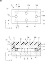
- FIG. 1A and FIG. 1B are a plan view of an acoustic wave device according to a first embodiment of the present invention and a cross-sectional view taken along the line BB in FIG. 1A.
- FIG. 2 is a diagram showing the relationship between the ratio D / H and the stress applied to the end portion in the longitudinal direction of the acoustic wave device when placed at a temperature of 85 ° C.
- FIG. 3 is a front sectional view of an acoustic wave device according to the second embodiment of the present invention.
- FIG. 4 is a front sectional view of an acoustic wave device according to a third embodiment of the present invention.
- FIG. 5 is a diagram showing a relationship between longitudinal positions of the piezoelectric substrate and the sealing resin layer in the elastic wave device according to the second embodiment and stress applied at high temperature.
- FIG. 6 is a diagram illustrating the relationship between the longitudinal positions of the piezoelectric substrate and the sealing resin layer in the elastic wave device according to the third embodiment and the stress applied at a high temperature.
- FIG. 7 is a plan view of an acoustic wave device according to a fourth embodiment of the present invention.
- FIG. 8 is a plan view of an acoustic wave device according to the fifth embodiment of the present invention.
- FIG. 1A and FIG. 1B are a plan view of an acoustic wave device according to a first embodiment of the present invention and a cross-sectional view taken along line BB in FIG. 1A.
- the acoustic wave device 1 has a mounting substrate 2.
- the mounting substrate 2 is made of insulating ceramics such as alumina or semiconductor ceramics. Further, the mounting substrate 2 may be formed of a material other than ceramics.
- a plurality of electrode lands 3 and 4 are provided on the upper surface of the mounting substrate 2.
- the electrode lands 3 and 4 are made of an appropriate metal such as Al, Cu, Ag, or an alloy thereof.
- the acoustic wave element 5 is mounted on the mounting substrate 2.
- the acoustic wave element 5 has a piezoelectric substrate 6.
- the piezoelectric substrate 6 is made of a piezoelectric single crystal such as lithium tantalate or lithium niobate. However, the piezoelectric substrate 6 may be made of piezoelectric ceramics.
- the piezoelectric substrate 6 has a first main surface 6a and a second main surface 6b facing each other.
- An IDT electrode 7 is provided on the first main surface 6a.
- a hollow portion A where the IDT electrode 7 faces is provided between the first main surface 6 a and the mounting substrate 2.
- the electrode lands 8 and 9 electrically connected to the IDT electrode 7 are provided on the first main surface 6a.
- the electrode lands 8 and 9 are joined to the electrode lands 3 and 4 by bumps 10 and 11.
- the electrode lands 8 and 9 are made of an appropriate metal or alloy.
- the bumps 10 and 11 are also made of an appropriate metal such as solder or Au.
- the acoustic wave device 1 is arranged so that the first main surface 6 a of the piezoelectric substrate 6 faces the mounting substrate 2. Thereby, the hollow part A mentioned above is formed.
- a sealing resin layer 12 is provided so as to cover the periphery of the acoustic wave element 5.
- the sealing resin layer 12 is made of an appropriate synthetic resin such as an epoxy resin.
- the sealing resin layer 12 is provided so as to cover the acoustic wave element 5 except for the hollow portion A.
- a recess 13a having an X-direction dimension of 10% with respect to the X-direction dimension of the surface 12a is provided on the surface 12a opposite to the mounting substrate 2 of the sealing resin layer 12.
- a plurality of recesses 13a to 13d are provided on the positions of the bumps 10, 11, 10A, 11A provided below the sealing resin layer 12 are indicated by broken-line circles. That is, the bumps 10 and 11 described above are located on both sides of the recess 13a. Bumps 10A and 11A are also located on both sides of the recess 13b.
- the sealing resin layer 12 and the piezoelectric substrate 6 have a rectangular planar shape having a long side and a short side.
- the bumps 10 and 11 are located on one end side and the other end side of one long side of the piezoelectric substrate 6.
- the recess 13a is located in the center on this long side.
- the bump 10A is located on one end side and the bump 11A is located on the other end side.
- the recess 13b is located in the center on this long side.
- a recess 13c is located at the center of the short side where the bumps 10 and 10A are located.
- a recess 13d is located at the center between the bumps 11 and 11A.
- the recesses 13a to 13d are located between a pair of adjacent bumps.
- Depth D is the depth of the recesses 13a to 13d, that is, the dimension from the surface 12a of the sealing resin layer 12 opposite to the mounting substrate 2 to the bottom surface of the recesses 13a to 13d.
- the distance between the surface 12a of the sealing resin layer 12 opposite to the mounting substrate 2 and the second main surface 6b of the piezoelectric substrate 6 is H.
- the ratio D / H of the depth D to the distance H is 1/3 or more.
- FIG. 2 shows an acoustic wave device at a high temperature of 85 ° C. when the ratio D / H between the depth D of the recesses 13a to 13d and the distance H is changed in the acoustic wave device 1 of the embodiment. It is a figure which shows the relationship with the stress added to the longitudinal direction edge part of 5.
- FIG. The stress at the end portion in the longitudinal direction is a value obtained by obtaining the stress at the end portion C in the longitudinal direction of the piezoelectric substrate 6 in a state where the acoustic wave device 1 has reached a steady state at a temperature of 85 ° C. .
- the depth D of the recesses 13a to 13d is provided so that the ratio D / H is 1/3 or more.
- the upper limit of the ratio D / H is not particularly limited in order to relieve the stress applied to the end portion.
- the distance between the surface 12a and the second main surface 6b of the piezoelectric substrate 6 is the upper limit of D. Therefore, the value of the ratio D / H is 1 or less.
- the value of the ratio D / H is less than 1. In that case, a sealing resin layer portion exists between the bottoms of the recesses 13 a to 13 d and the second main surface 6 b of the piezoelectric substrate 6. Thereby, it is possible to more effectively suppress the decrease in mechanical strength.
- the depths of all the recesses 13a to 13d are the same.
- FIG. 3 is a front sectional view of an elastic wave device 21 according to the second embodiment of the present invention
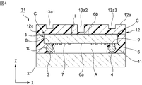
- FIG. 4 is a front sectional view of an elastic wave device 31 according to the third embodiment of the present invention.
- 3 and 4 are drawings corresponding to FIG. 1B shown in the first embodiment. The difference is that three concave portions 13a1 to 13a3 are provided on the surface 12a of the sealing resin layer 12 along the longitudinal direction of the piezoelectric substrate 6. Although not shown in FIGS. 3 and 4, three concave portions are similarly provided in the long side portion on the side where the concave portion 13 b shown in FIG. 1A is provided.
- the depths D of all the concave portions 13a1 to 13a3 are made equal.
- the depth of the concave portion 13a2 located at the center in the longitudinal direction of the piezoelectric substrate 6 is relatively deep, and is located on one end side and the other end side in the longitudinal direction.
- the depths of the recessed portions 13a1 and 13a3 are relatively shallow.
- the depth of the recess 13a1 is equal to the depth of the recess 13a3.
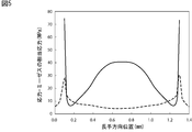
- 5 and 6 show the relationship between the longitudinal direction (X direction) position and the stress-Mises equivalent stress in the cross section shown in FIGS. 3 and 4 of the elastic wave devices 21 and 31 of the second and third embodiments. It is a figure which shows a relationship. 5 and 6, the solid line represents the stress applied to the piezoelectric substrate 6 on the second main surface 6 b of the piezoelectric substrate 6, and the broken line represents the sealing resin layer on the plane 12 c including the second main surface 6 b of the piezoelectric substrate 6. It is a figure which shows the applied stress.
- the piezoelectric substrate 6 located 0.1 mm away from the end portion of the sealing resin indicated by 0 on the horizontal axis due to thermal stress under high temperature. It turns out that a big stress is added to a longitudinal direction edge part. Even in the plane 12c including the sealing resin layer 12 and the second main surface 6b of the piezoelectric substrate 6, the stress is about 65 at the longitudinal position of 0.1 mm in the horizontal axis corresponding to the longitudinal end of the piezoelectric substrate 6. It can be seen that it is ⁇ 75 MPa, which is larger than the stress at other longitudinal positions.
- the stresses at both ends in the longitudinal direction of the piezoelectric substrate 6 are about 70 MPa and about 65 MPa, which are reduced compared to the case of FIG. 5. I understand that.
- the stress at the center in the longitudinal direction in FIG. 6 is larger than that in FIG. 5, and is about 40 to 45 MPa.
- the stress difference between the stress at both end positions of the second main surface 6b of the piezoelectric substrate 6 and the stress at the center position is smaller than the stress difference in the case of FIG.
- the elastic wave device 31 of the third embodiment can reduce the stress at the end portion in the large longitudinal direction and can achieve uniform stress corresponding to the entire longitudinal direction of the piezoelectric substrate 6.
- the central concave portion 13a2 can be made relatively deep. desirable. Even in this case, the depth D of all the recesses 13a1 to 13a3 needs to have a ratio D / H of 1/3 or more.
- the stress distribution state shown in FIG. 5 and FIG. 6 is the E-direction shown in FIG. 1 (a) passing through the short side direction of the piezoelectric substrate 6, specifically, the bumps 10 and 10A and the recess 13c of FIG. It has been confirmed that similar results can be obtained in the E section.
- FIG. 7 is a plan view of an elastic wave device 41 according to the fourth embodiment.
- recesses 13 a and 13 b are provided in the center of the long side of the piezoelectric substrate 6 in the longitudinal direction and in the vicinity of the center of the other long side.
- the formation position and number of the recesses in the present invention are not particularly limited.
- the concave portion provided on the upper surface of the sealing resin layer 12 is provided at a position that does not overlap with the hollow portion A located below when viewed in plan from the surface 12a side. More preferably, it is further desirable that it is provided so as not to overlap with the IDT electrode 7. Thereby, the mechanical strength of the acoustic wave device can be increased more effectively.
- the concave portions 13a to 13d, 13a1 to 13a3, and the like having a circular planar shape are shown, but the planar shape of the concave portions is not particularly limited and may be an arbitrary shape. it can.
- recesses 13e, 13f, 13g, and 13h that constitute letters and numbers may be provided as in the elastic wave device 51 of the fifth embodiment shown in FIG. In this case, since the recesses 13e to 13h can represent characters, numbers, and the like, markings indicating product information, product lot numbers, and the like can be formed.
Landscapes
- Physics & Mathematics (AREA)
- Acoustics & Sound (AREA)
- Chemical & Material Sciences (AREA)
- Engineering & Computer Science (AREA)
- Materials Engineering (AREA)
- Surface Acoustic Wave Elements And Circuit Networks Thereof (AREA)
Abstract
Description

2…実装基板
3,4…電極ランド
5…弾性波素子
6…圧電基板
6a,6b…第1,第2の主面
7…IDT電極
8,9…電極ランド
10,10A,11,11A…バンプ
12…封止樹脂層
12a…面
12c…平面
13a~13h,13a1~13a3…凹部
21,31,41,51…弾性波装置
Claims (7)
- 実装基板と、
前記実装基板上に設けられた電極ランドと、
対向し合う第1及び第2の主面を有する圧電基板と、前記圧電基板の前記第1の主面上に設けられたIDT電極とを有し、前記第1の主面が前記実装基板の前記電極ランドと隙間を隔てて対向するように前記実装基板に搭載された弾性波素子と、
前記弾性波素子を前記電極ランドに接合している複数のバンプと、
前記実装基板に搭載されている前記弾性波素子を覆うように設けられており、前記隙間の部分を中空部としている封止樹脂層とを備え、
前記封止樹脂層の前記実装基板とは反対側の面に、凹部が設けられており、前記凹部の深さが、前記圧電基板の前記第2の主面から、前記封止樹脂層の前記実装基板とは反対側の面までの距離の1/3以上である、弾性波装置。 - 前記封止樹脂層の前記実装基板とは反対側の面から平面視した場合に、前記凹部がバンプ間に位置している、請求項1に記載の弾性波装置。
- 前記複数のバンプにおいて、全てのバンプ間に前記凹部が位置している、請求項2に記載の弾性波装置。
- 前記凹部の底が、前記圧電基板の前記第2の主面よりも前記封止樹脂層の前記実装基板とは反対側の面の側に位置しており、前記凹部の底と前記圧電基板の前記第2の主面との間に封止樹脂層部分が存在している、請求項1~3のいずれか1項に記載の弾性波装置。
- 前記封止樹脂層の前記実装基板とは反対側の面から平面視した場合、前記凹部が、前記IDT電極が臨んでいる前記中空部外に位置している、請求項1~3のいずれか1項に記載の弾性波装置。
- 前記封止樹脂層の前記実装基板とは反対側の面から平面視した場合に、前記凹部が、前記IDT電極と重なり合っていない、請求項5に記載の弾性波装置。
- 前記凹部が、文字または数字を構成している、請求項1~6のいずれか1項に記載の弾性波装置。
Priority Applications (4)
| Application Number | Priority Date | Filing Date | Title |
|---|---|---|---|
| JP2016573628A JP6418256B2 (ja) | 2015-06-08 | 2016-03-29 | 弾性波装置 |
| CN201680033287.5A CN107636964B (zh) | 2015-06-08 | 2016-03-29 | 弹性波装置 |
| DE112016002575.0T DE112016002575B4 (de) | 2015-06-08 | 2016-03-29 | Vorrichtung für elastische Wellen |
| US15/828,462 US11228297B2 (en) | 2015-06-08 | 2017-12-01 | Elastic wave device |
Applications Claiming Priority (2)
| Application Number | Priority Date | Filing Date | Title |
|---|---|---|---|
| JP2015115799 | 2015-06-08 | ||
| JP2015-115799 | 2015-06-08 |
Related Child Applications (1)
| Application Number | Title | Priority Date | Filing Date |
|---|---|---|---|
| US15/828,462 Continuation US11228297B2 (en) | 2015-06-08 | 2017-12-01 | Elastic wave device |
Publications (1)
| Publication Number | Publication Date |
|---|---|
| WO2016199480A1 true WO2016199480A1 (ja) | 2016-12-15 |
Family
ID=57503456
Family Applications (1)
| Application Number | Title | Priority Date | Filing Date |
|---|---|---|---|
| PCT/JP2016/060116 Ceased WO2016199480A1 (ja) | 2015-06-08 | 2016-03-29 | 弾性波装置 |
Country Status (5)
| Country | Link |
|---|---|
| US (1) | US11228297B2 (ja) |
| JP (1) | JP6418256B2 (ja) |
| CN (1) | CN107636964B (ja) |
| DE (1) | DE112016002575B4 (ja) |
| WO (1) | WO2016199480A1 (ja) |
Cited By (2)
| Publication number | Priority date | Publication date | Assignee | Title |
|---|---|---|---|---|
| WO2018110057A1 (ja) * | 2016-12-16 | 2018-06-21 | 株式会社村田製作所 | 弾性波装置、高周波フロントエンド回路及び通信装置 |
| WO2019078234A1 (ja) * | 2017-10-19 | 2019-04-25 | 株式会社村田製作所 | 弾性波装置 |
Families Citing this family (1)
| Publication number | Priority date | Publication date | Assignee | Title |
|---|---|---|---|---|
| JP2017220582A (ja) * | 2016-06-08 | 2017-12-14 | ルネサスエレクトロニクス株式会社 | 半導体装置及びその製造方法 |
Citations (4)
| Publication number | Priority date | Publication date | Assignee | Title |
|---|---|---|---|---|
| JP2008109346A (ja) * | 2006-10-25 | 2008-05-08 | Kyocera Corp | 弾性表面波装置およびその製造方法 |
| JP2010177388A (ja) * | 2009-01-29 | 2010-08-12 | Panasonic Corp | 半導体装置及びその製造方法 |
| JP2011151553A (ja) * | 2010-01-20 | 2011-08-04 | Murata Mfg Co Ltd | 弾性波デュプレクサ |
| WO2013115115A1 (ja) * | 2012-02-03 | 2013-08-08 | 株式会社村田製作所 | 弾性表面波素子及びそれを備えた複合モジュール |
Family Cites Families (5)
| Publication number | Priority date | Publication date | Assignee | Title |
|---|---|---|---|---|
| JP3841304B2 (ja) * | 2004-02-17 | 2006-11-01 | セイコーエプソン株式会社 | 圧電発振器、及びその製造方法 |
| WO2011136070A1 (ja) * | 2010-04-27 | 2011-11-03 | 京セラ株式会社 | 弾性波装置およびその製造方法 |
| KR101645172B1 (ko) * | 2012-09-25 | 2016-08-03 | 가부시키가이샤 무라타 세이사쿠쇼 | 탄성파 장치 및 그 제조 방법 |
| JP6093163B2 (ja) | 2012-12-05 | 2017-03-08 | 新日本無線株式会社 | 中空構造を有する装置の製造方法及び検査方法 |
| CN105144578B (zh) * | 2013-05-01 | 2018-05-11 | 株式会社村田制作所 | 水晶振动装置及其制造方法 |
-
2016
- 2016-03-29 DE DE112016002575.0T patent/DE112016002575B4/de active Active
- 2016-03-29 WO PCT/JP2016/060116 patent/WO2016199480A1/ja not_active Ceased
- 2016-03-29 JP JP2016573628A patent/JP6418256B2/ja active Active
- 2016-03-29 CN CN201680033287.5A patent/CN107636964B/zh active Active
-
2017
- 2017-12-01 US US15/828,462 patent/US11228297B2/en active Active
Patent Citations (4)
| Publication number | Priority date | Publication date | Assignee | Title |
|---|---|---|---|---|
| JP2008109346A (ja) * | 2006-10-25 | 2008-05-08 | Kyocera Corp | 弾性表面波装置およびその製造方法 |
| JP2010177388A (ja) * | 2009-01-29 | 2010-08-12 | Panasonic Corp | 半導体装置及びその製造方法 |
| JP2011151553A (ja) * | 2010-01-20 | 2011-08-04 | Murata Mfg Co Ltd | 弾性波デュプレクサ |
| WO2013115115A1 (ja) * | 2012-02-03 | 2013-08-08 | 株式会社村田製作所 | 弾性表面波素子及びそれを備えた複合モジュール |
Cited By (8)
| Publication number | Priority date | Publication date | Assignee | Title |
|---|---|---|---|---|
| WO2018110057A1 (ja) * | 2016-12-16 | 2018-06-21 | 株式会社村田製作所 | 弾性波装置、高周波フロントエンド回路及び通信装置 |
| JPWO2018110057A1 (ja) * | 2016-12-16 | 2019-07-18 | 株式会社村田製作所 | 弾性波装置、高周波フロントエンド回路及び通信装置 |
| CN110100387A (zh) * | 2016-12-16 | 2019-08-06 | 株式会社村田制作所 | 弹性波装置、高频前端电路以及通信装置 |
| US20190288665A1 (en) * | 2016-12-16 | 2019-09-19 | Murata Manufacturing Co., Ltd. | Acoustic wave device, radio-frequency front end circuit, and communication device |
| US11005444B2 (en) | 2016-12-16 | 2021-05-11 | Murata Manufacturing Co., Ltd. | Acoustic wave device, radio-frequency front end circuit, and communication device |
| CN110100387B (zh) * | 2016-12-16 | 2023-06-06 | 株式会社村田制作所 | 弹性波装置、高频前端电路以及通信装置 |
| WO2019078234A1 (ja) * | 2017-10-19 | 2019-04-25 | 株式会社村田製作所 | 弾性波装置 |
| US11581868B2 (en) | 2017-10-19 | 2023-02-14 | Murata Manufacturing Co., Ltd. | Acoustic wave device |
Also Published As
| Publication number | Publication date |
|---|---|
| JP6418256B2 (ja) | 2018-11-07 |
| DE112016002575B4 (de) | 2023-08-24 |
| US20180102758A1 (en) | 2018-04-12 |
| US11228297B2 (en) | 2022-01-18 |
| DE112016002575T5 (de) | 2018-03-01 |
| CN107636964B (zh) | 2021-08-06 |
| CN107636964A (zh) | 2018-01-26 |
| JPWO2016199480A1 (ja) | 2017-06-22 |
Similar Documents
| Publication | Publication Date | Title |
|---|---|---|
| US11695388B2 (en) | Elastic wave device | |
| JP2006245989A (ja) | 弾性表面波装置 | |
| US20180102759A1 (en) | Elastic wave device | |
| JP6418256B2 (ja) | 弾性波装置 | |
| US11764753B2 (en) | Elastic wave device and electronic component | |
| JPWO2016158744A1 (ja) | 電子部品 | |
| JPWO2016158050A1 (ja) | 弾性波装置、通信モジュール機器及び弾性波装置の製造方法 | |
| JP6112505B2 (ja) | 圧電ウエハおよび圧電振動素子の製造方法 | |
| JP6017250B2 (ja) | 圧電デバイス | |
| JP5399888B2 (ja) | 音叉型屈曲水晶振動素子 | |
| JP6508217B2 (ja) | 基板、基板の製造方法及び弾性波装置 | |
| WO2014097681A1 (ja) | 圧電トランス装置 | |
| JP6544153B2 (ja) | 電子部品素子及び電子部品 | |
| JP6194804B2 (ja) | モールドパッケージ | |
| US10812041B2 (en) | Elastic wave device and manufacturing method for same | |
| JP5159820B2 (ja) | 水晶振動子 | |
| JP6176057B2 (ja) | 電子部品用パッケージのベース、電子部品用パッケージ | |
| JP5895928B2 (ja) | 電子部品用パッケージ及び圧電デバイス | |
| JP2015188147A (ja) | 導波管およびその製造方法 | |
| WO2018079485A1 (ja) | 弾性波装置 | |
| JP6276341B2 (ja) | 圧電振動素子および圧電ウエハ | |
| JP5780287B2 (ja) | 電子部品用パッケージ及び圧電デバイス | |
| JP2014239333A (ja) | 超音波発生器 | |
| JP6257150B2 (ja) | 電子部品パッケージ及び電子部品パッケージの製造方法 | |
| WO2015045906A1 (ja) | 水晶発振器 |
Legal Events
| Date | Code | Title | Description |
|---|---|---|---|
| ENP | Entry into the national phase |
Ref document number: 2016573628 Country of ref document: JP Kind code of ref document: A |
|
| 121 | Ep: the epo has been informed by wipo that ep was designated in this application |
Ref document number: 16807187 Country of ref document: EP Kind code of ref document: A1 |
|
| WWE | Wipo information: entry into national phase |
Ref document number: 112016002575 Country of ref document: DE |
|
| 122 | Ep: pct application non-entry in european phase |
Ref document number: 16807187 Country of ref document: EP Kind code of ref document: A1 |