WO2016199360A1 - 半導体装置 - Google Patents
半導体装置 Download PDFInfo
- Publication number
- WO2016199360A1 WO2016199360A1 PCT/JP2016/002512 JP2016002512W WO2016199360A1 WO 2016199360 A1 WO2016199360 A1 WO 2016199360A1 JP 2016002512 W JP2016002512 W JP 2016002512W WO 2016199360 A1 WO2016199360 A1 WO 2016199360A1
- Authority
- WO
- WIPO (PCT)
- Prior art keywords
- switching element
- terminal
- heat sink
- output current
- drive circuit
- Prior art date
- Legal status (The legal status is an assumption and is not a legal conclusion. Google has not performed a legal analysis and makes no representation as to the accuracy of the status listed.)
- Ceased
Links
Images



Classifications
-
- H—ELECTRICITY
- H02—GENERATION; CONVERSION OR DISTRIBUTION OF ELECTRIC POWER
- H02J—ELECTRIC POWER NETWORKS; CIRCUIT ARRANGEMENTS OR SYSTEMS FOR SUPPLYING OR DISTRIBUTING ELECTRIC POWER; SYSTEMS FOR STORING ELECTRIC ENERGY
- H02J4/00—Circuit arrangements for mains or distribution networks not specified as AC or DC; Circuit arrangements for mains or distribution networks combining AC and DC sections or sub-networks
- H02J4/20—Networks integrating separated AC and DC power sections
- H02J4/25—Networks integrating separated AC and DC power sections for transfer of electric power between AC and DC networks, e.g. for supplying the DC section within a load from an AC mains system
-
- H—ELECTRICITY
- H02—GENERATION; CONVERSION OR DISTRIBUTION OF ELECTRIC POWER
- H02M—APPARATUS FOR CONVERSION BETWEEN AC AND AC, BETWEEN AC AND DC, OR BETWEEN DC AND DC, AND FOR USE WITH MAINS OR SIMILAR POWER SUPPLY SYSTEMS; CONVERSION OF DC OR AC INPUT POWER INTO SURGE OUTPUT POWER; CONTROL OR REGULATION THEREOF
- H02M1/00—Details of apparatus for conversion
- H02M1/08—Circuits specially adapted for the generation of control voltages for semiconductor devices incorporated in static converters
- H02M1/088—Circuits specially adapted for the generation of control voltages for semiconductor devices incorporated in static converters for the simultaneous control of series or parallel connected semiconductor devices
-
- H—ELECTRICITY
- H02—GENERATION; CONVERSION OR DISTRIBUTION OF ELECTRIC POWER
- H02M—APPARATUS FOR CONVERSION BETWEEN AC AND AC, BETWEEN AC AND DC, OR BETWEEN DC AND DC, AND FOR USE WITH MAINS OR SIMILAR POWER SUPPLY SYSTEMS; CONVERSION OF DC OR AC INPUT POWER INTO SURGE OUTPUT POWER; CONTROL OR REGULATION THEREOF
- H02M7/00—Conversion of AC power input into DC power output; Conversion of DC power input into AC power output
- H02M7/003—Constructional details, e.g. physical layout, assembly, wiring or busbar connections
-
- H—ELECTRICITY
- H02—GENERATION; CONVERSION OR DISTRIBUTION OF ELECTRIC POWER
- H02M—APPARATUS FOR CONVERSION BETWEEN AC AND AC, BETWEEN AC AND DC, OR BETWEEN DC AND DC, AND FOR USE WITH MAINS OR SIMILAR POWER SUPPLY SYSTEMS; CONVERSION OF DC OR AC INPUT POWER INTO SURGE OUTPUT POWER; CONTROL OR REGULATION THEREOF
- H02M7/00—Conversion of AC power input into DC power output; Conversion of DC power input into AC power output
- H02M7/42—Conversion of DC power input into AC power output without possibility of reversal
- H02M7/44—Conversion of DC power input into AC power output without possibility of reversal by static converters
- H02M7/48—Conversion of DC power input into AC power output without possibility of reversal by static converters using discharge tubes with control electrode or semiconductor devices with control electrode
- H02M7/53—Conversion of DC power input into AC power output without possibility of reversal by static converters using discharge tubes with control electrode or semiconductor devices with control electrode using devices of a triode or transistor type requiring continuous application of a control signal
- H02M7/537—Conversion of DC power input into AC power output without possibility of reversal by static converters using discharge tubes with control electrode or semiconductor devices with control electrode using devices of a triode or transistor type requiring continuous application of a control signal using semiconductor devices only, e.g. single switched pulse inverters
-
- H—ELECTRICITY
- H10—SEMICONDUCTOR DEVICES; ELECTRIC SOLID-STATE DEVICES NOT OTHERWISE PROVIDED FOR
- H10W—GENERIC PACKAGES, INTERCONNECTIONS, CONNECTORS OR OTHER CONSTRUCTIONAL DETAILS OF DEVICES COVERED BY CLASS H10
- H10W40/00—Arrangements for thermal protection or thermal control
- H10W40/70—Fillings or auxiliary members in containers or in encapsulations for thermal protection or control
- H10W40/77—Auxiliary members characterised by their shape
- H10W40/778—Auxiliary members characterised by their shape in encapsulations
-
- H—ELECTRICITY
- H10—SEMICONDUCTOR DEVICES; ELECTRIC SOLID-STATE DEVICES NOT OTHERWISE PROVIDED FOR
- H10W—GENERIC PACKAGES, INTERCONNECTIONS, CONNECTORS OR OTHER CONSTRUCTIONAL DETAILS OF DEVICES COVERED BY CLASS H10
- H10W70/00—Package substrates; Interposers; Redistribution layers [RDL]
- H10W70/40—Leadframes
- H10W70/411—Chip-supporting parts, e.g. die pads
-
- H—ELECTRICITY
- H10—SEMICONDUCTOR DEVICES; ELECTRIC SOLID-STATE DEVICES NOT OTHERWISE PROVIDED FOR
- H10W—GENERIC PACKAGES, INTERCONNECTIONS, CONNECTORS OR OTHER CONSTRUCTIONAL DETAILS OF DEVICES COVERED BY CLASS H10
- H10W70/00—Package substrates; Interposers; Redistribution layers [RDL]
- H10W70/40—Leadframes
- H10W70/461—Leadframes specially adapted for cooling
-
- H—ELECTRICITY
- H10—SEMICONDUCTOR DEVICES; ELECTRIC SOLID-STATE DEVICES NOT OTHERWISE PROVIDED FOR
- H10W—GENERIC PACKAGES, INTERCONNECTIONS, CONNECTORS OR OTHER CONSTRUCTIONAL DETAILS OF DEVICES COVERED BY CLASS H10
- H10W70/00—Package substrates; Interposers; Redistribution layers [RDL]
- H10W70/40—Leadframes
- H10W70/481—Leadframes for devices being provided for in groups H10D8/00 - H10D48/00
-
- H—ELECTRICITY
- H10—SEMICONDUCTOR DEVICES; ELECTRIC SOLID-STATE DEVICES NOT OTHERWISE PROVIDED FOR
- H10W—GENERIC PACKAGES, INTERCONNECTIONS, CONNECTORS OR OTHER CONSTRUCTIONAL DETAILS OF DEVICES COVERED BY CLASS H10
- H10W72/00—Interconnections or connectors in packages
-
- H—ELECTRICITY
- H10—SEMICONDUCTOR DEVICES; ELECTRIC SOLID-STATE DEVICES NOT OTHERWISE PROVIDED FOR
- H10W—GENERIC PACKAGES, INTERCONNECTIONS, CONNECTORS OR OTHER CONSTRUCTIONAL DETAILS OF DEVICES COVERED BY CLASS H10
- H10W90/00—Package configurations
-
- H—ELECTRICITY
- H10—SEMICONDUCTOR DEVICES; ELECTRIC SOLID-STATE DEVICES NOT OTHERWISE PROVIDED FOR
- H10W—GENERIC PACKAGES, INTERCONNECTIONS, CONNECTORS OR OTHER CONSTRUCTIONAL DETAILS OF DEVICES COVERED BY CLASS H10
- H10W90/00—Package configurations
- H10W90/811—Multiple chips on leadframes
-
- H—ELECTRICITY
- H10—SEMICONDUCTOR DEVICES; ELECTRIC SOLID-STATE DEVICES NOT OTHERWISE PROVIDED FOR
- H10W—GENERIC PACKAGES, INTERCONNECTIONS, CONNECTORS OR OTHER CONSTRUCTIONAL DETAILS OF DEVICES COVERED BY CLASS H10
- H10W90/00—Package configurations
- H10W90/701—Package configurations characterised by the relative positions of pads or connectors relative to package parts
- H10W90/751—Package configurations characterised by the relative positions of pads or connectors relative to package parts of bond wires
- H10W90/753—Package configurations characterised by the relative positions of pads or connectors relative to package parts of bond wires between laterally-adjacent chips
Definitions
- This disclosure relates to a semiconductor device in which a plurality of switching elements are driven in parallel.
- a semiconductor device is conventionally known in which an IGBT and a MOSFET are connected in parallel and used as a switching element.
- this semiconductor device either the IGBT or the MOSFET is disposed in the vicinity of the control circuit, and the other is disposed in the distance.
- the element A arranged in the vicinity of the control circuit gives the gate control signal given from the control circuit to the element B arranged far away via the gate control signal.
- the element A with a short transmission distance of the gate control signal is turned on first, and the element B with a long transmission distance is turned on later.
- the element A arranged in the vicinity of the control circuit is an RC-IGBT (reverse conducting IGBT) and the element B is a MOSFET
- the MOSFET is connected via a diode reversely connected to the IGBT at turn-off. Therefore, it is not necessary to give the MOSFET a large rated current.
- This disclosure is intended to provide a semiconductor device in which a short-circuit tolerance of a predetermined switching element among a plurality of elements can be suppressed small in a semiconductor device in which a plurality of switching elements are driven in parallel.
- a semiconductor device includes a first switching element that controls a first terminal and a second terminal, an output current that flows between the first terminal and the second terminal, a first switching element, A second switching element connected in parallel; and a drive circuit unit that outputs a control signal to the first switching element and the second switching element and drives them independently.
- the drive circuit unit drives the first switching element and the second switching element in parallel.
- the second switching element connects the drive circuit unit and the first switching element to each other, and the first control signal path through which the control signal is energized.
- the second switching element outputs from the first terminal to the second terminal via the first switching element.
- the second output current path is longer than the first output current path.
- the wiring length from the first terminal to the second terminal via the second switching element is made longer than the wiring length passing through the first switching element.
- the current path passing through each switching element forms a parasitic inductor, according to the present disclosure, the inductive reactance of the second switching element viewed from the first terminal and the second terminal is changed to the reactance of the first switching element. Can be larger.
- the short circuit current flows to the first switching element having a low reactance. Therefore, the short circuit tolerance of the second switching element can be kept small.
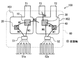
- FIG. 1 is a circuit diagram showing a schematic configuration of a semiconductor device according to a first embodiment. It is a top view which shows schematic structure of a semiconductor device. It is a top view which shows schematic structure of the semiconductor device concerning 2nd Embodiment.
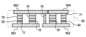
- FIG. 4 is a sectional view taken along line IV-IV in FIG. 3.
- 10 is a top view illustrating a schematic configuration of a semiconductor device according to Modification 1.
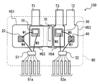
- FIG. 10 is a top view showing a schematic configuration of a semiconductor device according to Modification 2.
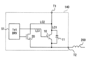
- FIG. It is a circuit diagram which shows schematic structure of the semiconductor device concerning 3rd Embodiment. It is a top view which shows schematic structure of a semiconductor device. It is a top view which shows schematic structure of the semiconductor device concerning other embodiment.
- the semiconductor device in this embodiment is, for example, an inverter that is inserted between a load and a DC power source and converts a DC voltage into an AC voltage.
- this semiconductor device 100 is a drive for supplying a voltage to the upper arm U and the lower arm L each composed of switching elements 10 to 40 and the gates of the switching elements 10 to 40 constituting each arm.
- An inverter circuit including the circuit unit 50 is configured.
- the semiconductor device 100 includes a first terminal T1 to which a power source on the high potential side is connected, and a third terminal T3 to which a power source having a lower potential than the first terminal T1 is connected.
- An IGBT 10 and an IGBT 30 are connected in series between the first terminal T1 and the third terminal T3.
- a MOSFET 20 is connected in parallel with the IGBT 10
- a MOSFET 40 is connected in parallel with the IGBT 30.
- a connection point between the IGBT 10 and the IGBT 30, that is, a connection point between the MOSFET 20 and the MOSFET 40 is connected to the second terminal T2.
- the IGBT 10 corresponds to a first switching element
- the MOSFET 20 corresponds to a second switching element
- the IGBT 30 corresponds to a third switching element
- the MOSFET 40 corresponds to a fourth switching element.
- the IGBT 10 in the present embodiment is a reverse conducting IGBT (RC-IGBT), and a free wheel diode 11 is connected between the emitter and collector of the IGBT 10 as shown in FIG.
- the IGBT 30 is a reverse conducting IGBT (RC-IGBT), and a free-wheeling diode 31 is connected between the emitter and collector of the IGBT 30.
- the IGBTs 10 and 30 are composed mainly of silicon, and the MOSFETs 20 and 40 are composed mainly of silicon carbide for the purpose of low loss.
- the IGBT 10 and the MOSFET 20 constitute an upper arm U
- the IGBT 30 and the MOSFET 40 constitute a lower arm L.
- an upper arm U and a lower arm L are alternately turned on and off by a drive circuit unit 50 which will be described later, and a DC voltage flowing between the first terminal T1 and the third terminal T3 is converted into an AC voltage. In this way, an alternating current flows through the load 200.
- the drive circuit unit 50 includes a first drive circuit unit (1st DRV) 51 and a second drive circuit unit (2nd DRV) 52.
- the first drive circuit unit 51 outputs a control signal to the IGBT 10 and the MOSFET 20. That is, the first drive circuit unit 51 applies a gate voltage to the gates of the IGBT 10 and the MOSFET 20.
- the first drive circuit unit 51 in the present embodiment controls the gate voltage so that the IGBT 10 is first turned on and the MOSFET 20 is turned on later.
- the silicon carbide MOSFET 20 whose on-resistance can be suppressed to be lower than that of the IGBT 10 causes a steady loss.
- the ON state of the upper arm U it is possible to suppress the steady loss as compared with the configuration driven only by the IGBT.
- the output current ratio between the IGBT 10 and the MOSFET 20 is large on the IGBT 10 side, and the chip size (physique) of the MOSFET 20 can be suppressed. Therefore, even if silicon carbide, which is generally said to be expensive, is used as a main component, an increase in cost can be avoided.
- the second drive circuit unit 52 outputs a control signal to the IGBT 30 and the MOSFET 40. That is, a gate voltage is applied to the gates of the IGBT 30 and the MOSFET 40. For the same reason as the first drive circuit unit 51, for example, when the lower arm L is turned on, the second drive circuit unit 52 controls the gate voltage so that the IGBT 30 is turned on first and the MOSFET 40 is turned on later. .
- the semiconductor device 100 is configured as an integral module in which the IGBTs 10 and 30, the MOSFETs 20 and 40, and the drive circuit unit 50 are insert-molded with a mold resin 60.
- the IGBT 10 and the MOSFET 20 are mounted on a first heat sink HS1 that functions as a heat sink.
- the IGBT 30 and the MOSFET 40 are mounted on a second heat sink HS2 that is electrically insulated from the first heat sink HS1.
- the first heat sink HS1 and the second heat sink HS2 are substantially rectangular plate-like members along a plane orthogonal to a predetermined virtual axis.
- the IGBT 10 and the MOSFET 20 are electrically connected to one surface of the first heat sink HS1 via a conductive adhesive such as solder.
- the IGBT 10 has a vertical electrode configuration, and the collector is connected to one surface of the first heat sink HS1.
- the MOSFET 20 has a drain connected to one surface of the first heat sink HS1.
- the back surface opposite to the one surface of the first heat sink HS1 is exposed to the outside air from the mold resin 60, and the heat generated by the switching elements 10 and 20 is dissipated.
- the first heat sink HS1 has a protruding portion that extends from the portion embedded in the mold resin 60 in a direction orthogonal to the virtual axis and protrudes outside the mold resin 60. This protrusion corresponds to the first terminal T1 shown in FIG. In the present embodiment, the first terminal T1 extends from a position near one corner of one side of the first heat sink HS1 having a substantially rectangular shape.
- the IGBT 30 and the MOSFET 40 are electrically connected to one surface of the second heat sink HS2 via a conductive adhesive.
- the IGBT 30 has a vertical electrode configuration, and the collector is connected to one surface of the second heat sink HS2. Further, the drain of the MOSFET 40 is connected to one surface of the second heat sink HS2.
- the back surface opposite to the one surface of the second heat sink HS2 is exposed to the outside air from the mold resin 60, and heat generated by the switching elements 30 and 40 is dissipated.
- the second heat sink HS2 also has a protruding portion that extends from the portion embedded in the mold resin 60 in a direction perpendicular to the virtual axis and protrudes outside the mold resin 60.
- This protrusion corresponds to the second terminal T2 shown in FIG.
- the second heat sink HS2 in the present embodiment is congruent to the first heat sink HS1 in shape including the protruding portion when viewed from the front in the virtual axis direction. That is, in the present embodiment, the first terminal T1 and the second terminal T2 extend in the same direction, and the second terminal T2 is in a translational symmetry position with respect to the first terminal T1 in the arrangement direction of the heat sinks HS1 and HS2. Is formed.
- the IGBT 10 is disposed on one surface of the first heat sink HS1 and in the vicinity of the root of the first terminal T1. That is, the IGBT 10 is mounted in the vicinity of one corner of the first heat sink HS1 in the planar layout as viewed from the front in the virtual axis direction. Note that the IGBT 10 is mounted so that the back side in FIG. 2 is a collector and the front side is an emitter and a gate.
- the MOSFET 20 is mounted at a diagonal position of the first heat sink HS1 with respect to the mounting position of the IGBT 10.
- the MOSFET 20 is mounted so that the back side in the drawing of FIG. 2 is the drain and the near side is the source and gate.
- the 1st drive circuit part 51 is a position adjacent to the 1st heat sink HS1, and is arranged on the opposite side to the projection direction of the 1st terminal T1.
- the emitter of the IGBT 10 and the source of the MOSFET 20 are connected to each other by a bonding wire W1.
- the emitter of the IGBT 10 is connected to the second heat sink HS2 through the bonding wire W2.
- the first drive circuit unit 51 supplies a gate voltage to the IGBT 10 via the bonding wire W3 and also supplies a gate voltage to the MOSFET 20 via the bonding wire W4.
- a command signal for transmitting a driving instruction from the outside to the first drive circuit unit 51 is input to the first drive circuit unit 51 by a bonding wire that is not given a reference sign from a control terminal 51 a that is insert-molded at one end of the mold resin 60. Has been.
- the IGBT 30 is disposed on one surface of the second heat sink HS ⁇ b> 2 and in the vicinity of one corner on the side close to the IGBT 10. That is, it is arranged near the corner opposite to the base of the second terminal T2. Note that the IGBT 30 is mounted so that the back side in FIG. 2 is a collector and the near side is an emitter and a gate.
- the MOSFET 40 is mounted at a diagonal position of the second heat sink HS2 with respect to the mounting position of the IGBT 30.
- the MOSFET 40 is mounted so that the back side in the drawing of FIG. 2 is the drain and the front side is the source and gate.
- the 2nd drive circuit part 52 is the position adjacent to 2nd heat sink HS2, and is arrange
- the emitter of the IGBT 30 and the source of the MOSFET 40 are connected to each other by a bonding wire W5.
- the second drive circuit unit 52 supplies the gate voltage to the IGBT 30 via the bonding wire W6 and also supplies the gate voltage to the MOSFET 40 via the bonding wire W7.
- the emitter of the IGBT 30 is connected to a third terminal T3 that extends in the same direction as the first terminal T1 and the second terminal T2 and is electrically insulated from the heat sinks HS1 and HS2 via a bonding wire W8. ing. As shown in FIG.
- the third terminal T3 is disposed so as to be sandwiched between the first terminal T1 and the second terminal T2 in the direction in which the heat sinks HS1 and HS2 are arranged. Therefore, the bonding wire W8 is bonded so as to extend substantially in parallel with the protruding direction of each of the terminals T1 to T3.
- a command signal for transmitting a driving instruction from the outside to the second drive circuit unit 52 is input to the second drive circuit unit 52 by a bonding wire that does not give a reference sign from a control terminal 52 a that is insert-molded in the mold resin 60 at one end. Has been.
- a first control signal path LS1 shown in FIG. 1 for outputting a control signal from the first drive circuit unit 51 to the gate of the IGBT 10 is formed by a bonding wire W3 shown in FIG.
- the first output current path LC1 shown in FIG. 1 through which the output current of the IGBT 10 flows from the first terminal T1 through the IGBT 10 to the second terminal T2 in FIG. 2 passes through the IGBT 10 from the first terminal T1 in FIG. Further, the current path reaches the second terminal T2 via the bonding wire W2.
- the second output current path LC2 shown in FIG. 1 through which the output current of the MOSFET 20 flows from the first terminal T1 through the MOSFET 20 to the second terminal T2 is shown in FIG. 2 through the first heat sink HS1 from the first terminal T1. This is a current path from the emitter of the IGBT 10 via the bonding wire W1 to the second terminal T2 via the bonding wire W2.
- the second control signal path LS2 shown in FIG. 1 for outputting a control signal from the second drive circuit unit 52 to the gate of the IGBT 30 is formed by the bonding wire W6 shown in FIG.
- the third output current path LC3 shown in FIG. 1 through which the output current of the IGBT 30 flows from the second terminal T2 via the IGBT 30 to the third terminal T3 is shown in FIG. 2, via the IGBT 30 from the second terminal T2. Further, the current path reaches the third terminal T3 via the bonding wire W8.
- the fourth output current path LC4 shown in FIG. 1 through which the output current of the MOSFET 40 flows from the second terminal T2 via the MOSFET 40 to the third terminal T3 is shown in FIG. 2 through the second heat sink HS2 from the second terminal T2. This is a current path from the emitter of the IGBT 30 via the bonding wire W5 to the third terminal T3 via the bonding wire W8.
- the MOSFET 20 that is the second switching element is placed at a position that does not overlap the bonding wire W3 that forms the first control signal path LS1 when viewed from the front in the virtual axis direction. Further, when viewed from the front in the virtual axis direction, the MOSFET 20 is on the current path from the first terminal T1 via the IGBT 10 to the second terminal T2 via the bonding wire W2, that is, via the first output current via LC1. It is placed in a position that does not overlap. That is, the MOSFET 20 is mounted at a position excluding the first control signal path LS1, and is mounted at a position excluding the first output current path LC1.
- MOSFET 20 is mounted at a position farther than the IGBT 10 from the first terminal T1 and the second terminal T2.
- the second output current path LC2 from the first terminal T1 to the second terminal T2 via the MOSFET 20 is first as much as the current path in the first heat sink HS1 from the first terminal T1 to the MOSFET 20 and the bonding wire W1. It is longer than the output current path LC1.
- the MOSFET 40 as the fourth switching element is placed at a position that does not overlap the bonding wire W6 forming the second control signal path LS2 when viewed from the front in the virtual axis direction. Further, the MOSFET 40, when viewed from the front in the imaginary axis direction, on the current path from the second terminal T2 via the IGBT 30 to the third terminal T3 via the bonding wire W8, that is, via the third output current via LC3. It is placed in a position that does not overlap. That is, the MOSFET 40 is mounted at a position excluding the second control signal path LS2, and is mounted at a position excluding the third output current path LC3.
- MOSFET 40 is mounted at a position farther than the IGBT 30 from the second terminal T2 and the third terminal T3.
- the fourth output current path LC4 from the second terminal T2 via the MOSFET 40 to the third terminal T3 is third as much as the current path in the second heat sink HS2 from the second terminal T2 to the MOSFET 40 and the bonding wire W5. It is longer than the output current path LC3.
- the second output current path LC2 is longer than the first output current path LC1.
- the wiring length from the first terminal T1 through the MOSFET 20 to the second terminal T2 is longer than the wiring length through the IGBT 10.
- the current path passing through each switching element forms a parasitic inductor.
- the wiring length from the second terminal T2 via the MOSFET 40 to the third terminal T3 is longer than the wiring length via the IGBT 30.
- the inductive reactance of the MOSFET 40 viewed from the second terminal T2 and the third terminal T3 can be made larger than the reactance of the IGBT 30.
- the short circuit current flows to the IGBT 10 or the IGBT 30 having a low reactance. Therefore, the short circuit tolerance of the MOSFETs 20 and 40 can be suppressed.
- MOSFET20,40 since the short circuit tolerance of MOSFET20,40 can be suppressed, the physique of MOSFET20,40 can be made smaller than before. For example, even if the MOSFETs 20 and 40 are mainly composed of silicon carbide, which is generally said to be expensive, the increase in cost can be suppressed.
- the semiconductor device 100 includes the first heat sink HS1 and the second heat sink HS2 and the wiring is realized by the bonding wires W1 to W8 has been described.
- the semiconductor device 110 includes a third heat sink HS3 and a fourth heat sink HS4 as shown in FIGS.
- the third heat sink HS3 is formed to face most of the first heat sink HS1, and the IGBT 10 and the MOSFET 20 are sandwiched between the first heat sink HS1 and the third heat sink HS3.
- the third heat sink HS ⁇ b> 3 and the switching elements 10 and 20 are electrically connected to each other via a spacer 70.
- the third heat sink HS3 and the spacer 70 are connected to each other via a conductive adhesive 71 such as solder, and the spacer 70 and each switching element 10 and 20 are connected to each other via the conductive adhesive 71.
- the emitter of the IGBT 10 and the source of the MOSFET 20 are connected to each other by the third heat sink HS3.
- the third heat sink HS3 functions as the bonding wire W1 in the first embodiment and also functions as a heat sink.
- the fourth heat sink HS4 is formed to face most of the first heat sink HS1, and is disposed in the same plane on which the third heat sink HS3 is formed.
- the IGBT 30 and the MOSFET 40 are sandwiched between the second heat sink HS2 and the fourth heat sink HS4.
- the fourth heat sink HS ⁇ b> 4 and the switching elements 30 and 40 are electrically connected to each other via a spacer 70.
- the fourth heat sink HS4 and the spacer 70 are connected to each other via a conductive adhesive 71 such as solder, and the spacer 70 and each switching element 30, 40 are connected to each other via the conductive adhesive 71. Yes.
- the emitter of the IGBT 30 and the source of the MOSFET 40 are connected to each other by the fourth heat sink HS4.
- the fourth heat sink HS4 functions as the bonding wire W5 in the first embodiment, and also functions as a heat sink.
- the fourth heat sink HS4 has a protruding portion that protrudes at a position that does not overlap the second terminal T2 when viewed from the front in the virtual axis direction. This protrusion corresponds to the third terminal T3 in this modification. That is, the fourth heat sink HS4 has the function of the bonding wire W8 in the first embodiment.
- 3rd heat sink HS3 and 2nd heat sink HS2 are electrically connected by the spacer 70.
- the spacer 70 that connects the third heat sink HS3 and the second heat sink HS2 corresponds to the bonding wire W2 in the first embodiment.
- the third heat sink HS2 and the fourth heat sink HS4 are insert-molded by the mold resin 60, but the surfaces to which the switching elements 10 to 40 are not connected are exposed to the outside. Therefore, the semiconductor device 110 according to the present embodiment is configured so that the switching elements 10 to 40 are sandwiched between the heat sinks HS1 to HS4 and formed in a card shape, and can dissipate heat on both sides.
- the arrangement of the switching elements 10 to 40 is substantially the same as in the first embodiment.
- the first output current path LC1 and the second output current path LC2 are larger or smaller than the first embodiment.
- the inductive reactance of the MOSFET 20 viewed from the first terminal T1 and the second terminal T2 can be made larger than the reactance of the IGBT 10. Further, the inductive reactance of the MOSFET 40 viewed from the second terminal T2 and the third terminal T3 can be made larger than the reactance of the IGBT 30. Thereby, since the short circuit tolerance of MOSFET20,40 can be suppressed, the physique of MOSFET20,40 can be made smaller than before.
- the semiconductor device 120 in this modification has a structure in which the shape of each heat sink HS1 to HS4 in the second embodiment having a rectangular shape is replaced with an L shape.
- the first heat sink HS1 and the third heat sink HS3 are formed by the IGBT 10 and the MOSFET 20 among the four corners of the first heat sink HS1 and the third heat sink HS3 that are rectangular in the first embodiment or the second embodiment. Two corners that are not arranged and one corner on the base side of the first terminal T1 are cut off to form an L shape as a whole.
- the second heat sink HS2 and the fourth heat sink HS4 are arranged. Two corners that are not formed and one corner on the base side of the first terminal T1 are cut off to form an L shape as a whole.
- the charge flowing from the first terminal T1 to the MOSFET 20 can travel linearly in the first heat sink HS1, but in this modification, it moves along the L shape.
- the electric charge flowing from the MOSFET 20 to the IGBT 10 can linearly travel through the third heat sink HS3.
- the second output current path LC2 can be made longer than in the second embodiment. Therefore, the inductive reactance of the MOSFET 20 viewed from the first terminal T1 and the second terminal T2 can be increased as compared with the second embodiment, and the amount of short-circuit current flowing into the MOSFET 20 can be suppressed.
- the fourth output current path LC4 can be lengthened as compared with the configuration of the second embodiment in which the heat sink can be linearly advanced in the heat sink. Therefore, the inductive reactance of the MOSFET 40 viewed from the second terminal T2 and the third terminal T3 can be increased as compared with the second embodiment, and the amount of short-circuit current flowing into the MOSFET 40 can be suppressed.
- the semiconductor device 130 according to the present modification includes the third heat sink HS3 and the fourth heat sink HS4 as in the second embodiment, but includes the emitter of the IGBT 10 and the source of the MOSFET 20.
- the connection between the emitter of the IGBT 30 and the source of the MOSFET 40 is carried by the bonding wire W5, as in the first embodiment.
- connection by the spacer 70 between the third heat sink HS3 and the second heat sink HS2 and the point that the third terminal T3 protrudes from the fourth heat sink HS4 are the same as in the second embodiment.
- the bonding wire is sufficiently thinner than the heat sink, and the current density when the current flows inside becomes larger in the bonding wire. If a short circuit between the collector and emitter occurs in the IGBT 10 and a short-circuit current flows between the first terminal T1 and the second terminal T2, the current density of the current flowing in the bonding wire W1 in this modification is the second embodiment. It becomes larger than the third heat sink HS3 in the form or modification 1. For this reason, when a short circuit occurs, the bonding wire W1 can be cut by heat generated by the resistance of the bonding wire W1. That is, the bonding wire W1 can function as a fuse. The same applies to the case where a short circuit between the second terminal T2 and the third terminal T3 occurs due to the occurrence of a collector-emitter short circuit in the IGBT 30, and the bonding wire W5 can function as a fuse. .
- the MOSFET 20 or the MOSFET 40 can be protected against overcurrent.
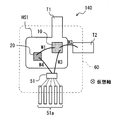
- the semiconductor device 140 in this embodiment does not have a configuration corresponding to the lower arm L in the first embodiment, as shown in FIG. That is, the semiconductor device 140 functions as a simple switch that turns on and off the supply of current to the load 200.
- an output current controlled by the IGBT 10 or the MOSFET 20 flows between the first terminal T1 and the second terminal T2. Since the circuit configuration of the semiconductor device 140 is different from the first embodiment only in that the lower arm L does not exist, detailed description thereof is omitted.
- the mounting layout of the semiconductor device 140 is different from that of the semiconductor device 100 of the first embodiment in that the second heat sink HS2, the IGBT 30, the MOSFET 40, the second drive circuit unit 52, and those The layout is such that bonding wires W5 to W8 provided for electrical connection are removed.
- the bonding wire W2 taken out from the emitter of the IGBT 10 is connected to a second terminal T2 that is electrically insulated from the first heat sink HS1.
- These components are insert-molded with a molding resin 60 with a part of the first terminal T1, the second terminal T2, and the control terminal 51a protruding outside.
- the second output current path LC2 is longer than the first output current path LC1.
- the wiring length from the first terminal T1 through the MOSFET 20 to the second terminal T2 is longer than the wiring length through the IGBT 10. Therefore, the inductive reactance of the MOSFET 20 viewed from the first terminal T1 and the second terminal T2 can be made larger than the reactance of the IGBT 10.
- the short-circuit current flows to the IGBT 10 having a low reactance. Therefore, the short circuit tolerance of the MOSFET 20 can be suppressed.
- MOSFET20 since the short circuit tolerance of MOSFET20 can be suppressed, the physique of MOSFET20 can be made smaller than before. For example, even if the MOSFET 20 is mainly composed of silicon carbide, which is generally said to be expensive, the increase in cost can be suppressed.
- the inverter or the switch is configured as a module with a built-in drive circuit unit in which the drive circuit unit 50 is embedded in the mold resin 60.
- the drive circuit unit 50 is not necessarily built in the mold resin 60.
- the input terminal 50a to which the gate voltage is input from the mold resin 60 is configured to protrude.
- the switching elements 10 to 40 and the drive circuit unit 50 are arranged so as not to overlap each other in a predetermined virtual plane orthogonal to the virtual axis.
- the length of LC2 is made longer than LC1 and the length of LC4 is made longer than LC3
- the switching elements 10 to 40 and the drive circuit unit 50 may be arranged at mutually different coordinates in the direction along the virtual axis.
Landscapes
- Engineering & Computer Science (AREA)
- Power Engineering (AREA)
- Inverter Devices (AREA)
Abstract
半導体装置は、第1端子(T1)および第2端子(T2)と、第1端子と第2端子との間に流れる出力電流を制御する第1スイッチング素子(10)と、第1スイッチング素子と並列接続された第2スイッチング素子(20)と、第1スイッチング素子と第2スイッチング素子とに制御信号を出力して、それぞれ独立に駆動する駆動回路部(50)と、を備える。駆動回路部は第1スイッチング素子と第2スイッチング素子とを並列に駆動させる。第2スイッチング素子は、駆動回路部と第1スイッチング素子とを互いに結んで制御信号が通電する第1制御信号経路(LS1)、および、第1端子から第1スイッチング素子を経由して第2端子に至って出力電流が通電する第1出力電流経路(LC1)、を除く部分であって、且つ、第1端子および第2端子からの距離が、第1スイッチング素子よりも遠い位置に配置され、第1端子から第2スイッチング素子を経由して第2端子に至って出力電流が通電する第2出力電流経路(LC2)が、第1出力電流経路よりも長くされている。
Description
本出願は、2015年6月9日に出願された日本出願番号2015-116936号に基づくもので、ここにその記載内容を援用する。
本開示は、複数のスイッチング素子が並列で駆動される半導体装置に関する。
特許文献1のように、従来から、IGBTとMOSFETとを並列接続してスイッチング素子として用いる半導体装置が知られている。この半導体装置は、IGBTとMOSFETのいずれか一方が、制御回路の近傍に配置され、他方が遠方に配置されている。そして、制御回路の近傍に配置された素子Aは、制御回路から与えられたゲート制御信号を仲介して、遠方に配置された素子Bに与える。
これによれば、各々の素子のゲートにゲート制御信号が与えられるとき、ゲート制御信号の伝達距離の短い素子Aが先にオンし、伝達距離の長い素子Bが追ってオンするようにできる。また、例えば、制御回路の近傍に配置された素子AがRC-IGBT(逆導通IGBT)であり、素子BがMOSFETであると仮定すると、ターンオフ時には、IGBTに逆接続されたダイオードを介してMOSFETが先にオフするため、MOSFETに大きな定格電流を持たせる必要がない。
ところで、特許文献1に記載の半導体装置では、平面レイアウトとして、スイッチング素子の出力電流が流れる電源ラインと制御回路との間にIGBTおよびMOSFETが実装されている。このため、スイッチング素子の出力端子間にショート故障が発生した場合に、制御回路に対して遠方、すなわち電源ラインの近傍に配置されたMOSFETに過電流が流れる虞がある。この過電流への耐量を確保するためにMOSFETの体格が大きくなってしまうことが懸念される。とくに、近年、低損失のシリコンカーバイド(SiC)を主成分として構成された素子が利用されつつあるが、シリコンカーバイドは高価であるため、素子サイズの拡大はコスト高に直結してしまう。
本開示は、複数のスイッチング素子が並列で駆動する半導体装置において、複数の素子のうち所定のスイッチング素子の短絡耐量を小さく抑えることのできる半導体装置を提供することを目的とする。
本開示の一態様によれば、半導体装置は、第1端子および第2端子と、第1端子と第2端子との間に流れる出力電流を制御する第1スイッチング素子と、第1スイッチング素子と並列接続された第2スイッチング素子と、第1スイッチング素子と第2スイッチング素子とに制御信号を出力して、それぞれ独立に駆動する駆動回路部と、を備える。駆動回路部は第1スイッチング素子と第2スイッチング素子とを並列に駆動させる。第2スイッチング素子は、駆動回路部と第1スイッチング素子とを互いに結んで制御信号が通電する第1制御信号経路、および、第1端子から第1スイッチング素子を経由して第2端子に至って出力電流が通電する第1出力電流経路、を除く部分であって、且つ、第1端子および第2端子からの距離が、第1スイッチング素子よりも遠い位置に配置され、第1端子から第2スイッチング素子を経由して第2端子に至って出力電流が通電する第2出力電流経路が、第1出力電流経路よりも長くされている。
上記したように、第2出力電流経路は第1出力電流経路よりも長くされている。換言すれば、第1端子から第2スイッチング素子を経由して第2端子に至る配線長が、第1スイッチング素子を経由する配線長に較べて長くされている。各スイッチング素子を経由する電流経路は寄生的なインダクタを形成するが、本開示によれば、第1端子および第2端子から見た第2スイッチング素子の誘導性リアクタンスを、第1スイッチング素子のリアクタンスよりも大きくすることができる。
よって、仮にスイッチング素子に短絡が発生した場合であっても、その短絡電流はリアクタンスの低い第1スイッチング素子側に流れることになる。したがって、第2スイッチング素子の短絡耐量を小さく抑えることができる。
以下、本開示の実施の形態を図面に基づいて説明する。なお、以下の各図相互において、互いに同一もしくは均等である部分に、同一符号を付与する。なお、上面図各図において、スイッチング素子の配置の認識を容易にするため、ハッチングを付している。
(第1実施形態)
最初に、図1および図2を参照して、本実施形態に係る半導体装置の概略構成について説明する。
最初に、図1および図2を参照して、本実施形態に係る半導体装置の概略構成について説明する。
本実施形態における半導体装置は、例えば、負荷と直流電源との間に介挿されて直流電圧を交流電圧に変換するインバータである。
先ず、図1を参照して、半導体装置100の回路構成について説明する。図1に示すように、この半導体装置100は、それぞれスイッチング素子10~40で構成された上アームUおよび下アームLと、各アームを構成するスイッチング素子10~40のゲートに電圧を供給する駆動回路部50を備えるインバータ回路として構成されている。
具体的には、半導体装置100は、高電位側の電源が接続される第1端子T1と、第1端子T1よりも低電位の電源が接続される第3端子T3と、を備えている。第1端子T1と第3端子T3の間には、IGBT10とIGBT30とが直列に接続されている。そして、IGBT10と並列にMOSFET20が接続され、IGBT30と並列にMOSFET40が接続されている。IGBT10とIGBT30との接続点、すなわちMOSFET20とMOSFET40との接続点は第2端子T2に接続されている。IGBT10は第1スイッチング素子に相当し、MOSFET20は第2スイッチング素子に相当し、IGBT30は第3スイッチング素子に相当し、MOSFET40は第4スイッチング素子に相当する。
本実施形態におけるIGBT10は逆導通IGBT(RC-IGBT)であり、図1に示すように、IGBT10のエミッタ-コレクタ間に還流ダイオード11が接続されている。同様に、IGBT30は逆導通IGBT(RC-IGBT)であり、IGBT30のエミッタ-コレクタ間に還流ダイオード31が接続されている。本実施形態では、IGBT10,30はシリコンを主成分として構成され、MOSFET20,40は、低損失を目的にシリコンカーバイドを主成分として構成されている。
図1に示すように、IGBT10およびMOSFET20が上アームUを構成しており、IGBT30およびMOSFET40が下アームLを構成している。そして、後述の駆動回路部50によって上アームUと下アームLが交互にオンオフされ、第1端子T1と第3端子T3の間に流れる直流電圧が交流電圧に変換されるようになっている。このようにして、負荷200には交流電流が流れる。
駆動回路部50は、第1駆動回路部(1st DRV)51と第2駆動回路部(2nd DRV)52とを有している。第1駆動回路部51はIGBT10およびMOSFET20に制御信号を出力している。すなわち、第1駆動回路部51がIGBT10およびMOSFET20のゲートにゲート電圧を印加している。本実施形態における第1駆動回路部51は、例えば、上アームUのターンオンに際して、最初にIGBT10をオンし、追ってMOSFET20をオンするようにゲート電圧を制御している。これは、オン抵抗がIGBT10よりも低く抑制できるシリコンカーバイドのMOSFET20に定常損失を担わせるためである。これにより、上アームUのオン状態において、IGBTのみで駆動される構成に較べて、定常損失を抑制することができる。
また、IGBT10とMOSFET20の出力電流比はIGBT10側が大きく、MOSFET20のチップサイズ(体格)は抑制できる。よって、一般に高価と云われるシリコンカーバイドを主成分としても、コストアップを回避できる。
第2駆動回路部52はIGBT30およびMOSFET40に制御信号を出力している。すなわち、IGBT30およびMOSFET40のゲートにゲート電圧を印加している。第1駆動回路部51と同様の理由により、第2駆動回路部52は、例えば、下アームLのターンオンに際して、最初にIGBT30をオンし、追ってMOSFET40をオンするようにゲート電圧を制御している。
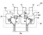
次いで、図2を参照して、半導体装置100の実装レイアウトについて説明する。本実施形態における半導体装置100は、IGBT10,30、MOSFET20,40、および駆動回路部50がモールド樹脂60によりインサート成型されてなる一体のモジュールとして構成されている。なお、図2に示すように、IGBT10およびMOSFET20は、放熱板として機能する第1ヒートシンクHS1に載置されている。同様に、IGBT30およびMOSFET40は、第1ヒートシンクHS1とは電気的に絶縁された第2ヒートシンクHS2に載置されている。
第1ヒートシンクHS1および第2ヒートシンクHS2は、所定の仮想軸に対して直交する面に沿った略長方形の板状部材である。IGBT10およびMOSFET20は第1ヒートシンクHS1の一面にはんだ等の導電性接着剤を介して電気的に接続されている。具体的には、IGBT10は縦型の電極構成を成し、コレクタが第1ヒートシンクHS1の一面に接続されている。また、MOSFET20はドレインが第1ヒートシンクHS1の一面に接続されている。一方、第1ヒートシンクHS1の一面と反対の裏面はモールド樹脂60から外気に露出しており、スイッチング素子10,20の発熱を放熱している。
さらに、第1ヒートシンクHS1は、モールド樹脂60に埋め込まれた部分から、仮想軸の直交する方向に延びてモールド樹脂60の外部に突出した突出部を有している。この突出部が図1に示す第1端子T1に相当する。本実施形態では、第1端子T1は、略長方形を成す第1ヒートシンクHS1の一辺うち、一つの角に近い位置から延びている。
同様に、IGBT30およびMOSFET40は第2ヒートシンクHS2の一面に導電性接着剤を介して電気的に接続されている。具体的には、IGBT30は縦型の電極構成を成し、コレクタが第2ヒートシンクHS2の一面に接続されている。また、MOSFET40はドレインが第2ヒートシンクHS2の一面に接続されている。一方、第2ヒートシンクHS2の一面と反対の裏面はモールド樹脂60から外気に露出しており、スイッチング素子30,40の発熱を放熱している。
さらに、第2ヒートシンクHS2も第1ヒートシンクHS1と同様に、モールド樹脂60に埋め込まれた部分から仮想軸の直交する方向に延びてモールド樹脂60の外部に突出した突出部を有している。この突出部が図1に示す第2端子T2に相当する。本実施形態における第2ヒートシンクHS2は、仮想軸方向から正面視したとき、突出部を含めた形状が第1ヒートシンクHS1と合同である。つまり、本実施形態では、第1端子T1と第2端子T2が互いに同一方向に延びており、第2端子T2は、ヒートシンクHS1,HS2の並び方向において、第1端子T1と並進対称な位置に形成されている。
各スイッチング素子10~40の具体的な配置について説明する。IGBT10は、図2に示すように、第1ヒートシンクHS1の一面上であって、第1端子T1の付け根近傍に配置されている。つまり、仮想軸方向から正面視した平面レイアウトにおいて、IGBT10は、第1ヒートシンクHS1の一つの角の近傍に実装されている。なお、IGBT10は、図2を示す紙面奥側がコレクタであり、手前側がエミッタおよびゲートになるように実装されている。
一方、MOSFET20は、IGBT10の実装位置に対して、第1ヒートシンクHS1の対角位置に実装されている。なお、MOSFET20は、図2を示す紙面奥側がドレインであり、手前側がソースおよびゲートになるように実装されている。
そして、第1駆動回路部51は、第1ヒートシンクHS1に隣り合う位置であって、第1端子T1の突出方向とは反対側に配置されている。
IGBT10のエミッタとMOSFET20のソースは互いにボンディングワイヤW1で接続されている。また、IGBT10のエミッタはボンディングワイヤW2を介して第2ヒートシンクHS2に接続されている。さらに、第1駆動回路部51はボンディングワイヤW3を介してIGBT10にゲート電圧を供給するとともに、ボンディングワイヤW4を介してMOSFET20にゲート電圧を供給している。
なお、外部から第1駆動回路部51へ駆動の指示を伝達する指令信号は、一端がモールド樹脂60にインサート成型された制御端子51aから符号を付与しないボンディングワイヤにより第1駆動回路部51へ入力されている。
IGBT30は、図2に示すように、第2ヒートシンクHS2の一面上であって、IGBT10に近い側の一角近傍に配置されている。つまり、第2端子T2の付け根と反対側の角近傍に配置されている。なお、IGBT30は、図2を示す紙面奥側がコレクタであり、手前側がエミッタおよびゲートになるように実装されている。
一方、MOSFET40は、IGBT30の実装位置に対して、第2ヒートシンクHS2の対角位置に実装されている。なお、MOSFET40は、図2を示す紙面奥側がドレインであり、手前側がソースおよびゲートになるように実装されている。
そして、第2駆動回路部52は、第2ヒートシンクHS2に隣り合う位置であって、第2端子T2の突出方向とは反対側に配置されている。
IGBT30のエミッタとMOSFET40のソースは互いにボンディングワイヤW5で接続されている。また、第2駆動回路部52はボンディングワイヤW6を介してIGBT30にゲート電圧を供給するとともに、ボンディングワイヤW7を介してMOSFET40にゲート電圧を供給している。さらに、IGBT30のエミッタは、第1端子T1や第2端子T2と同一方向に延設され、ヒートシンクHS1,HS2とは電気的に絶縁された第3端子T3に、ボンディングワイヤW8を介して接続されている。第3端子T3は、図2に示すように、ヒートシンクHS1,HS2の並び方向において、第1端子T1と第2端子T2との間に挟まれるように配置されている。よって、ボンディングワイヤW8は、各端子T1~T3の突出方向と略並行に延びるようにボンディングされる。
なお、外部から第2駆動回路部52へ駆動の指示を伝達する指令信号は、一端がモールド樹脂60にインサート成型された制御端子52aから符号を付与しないボンディングワイヤにより第2駆動回路部52へ入力されている。
次いで、図1に示す回路図と図2に示す実装レイアウトとの対応関係について説明する。第1駆動回路部51からIGBT10のゲートに制御信号を出力するための、図1に示す第1制御信号経路LS1は、図2に示すボンディングワイヤW3により形成される。
また、第1端子T1からIGBT10を経由し第2端子T2に至ってIGBT10の出力電流が流れる、図1に示す第1出力電流経路LC1は、図2において、第1端子T1からIGBT10を経由し、さらにボンディングワイヤW2を経由して第2端子T2に至る電流経路である。
また、第1端子T1からMOSFET20を経由し第2端子T2に至ってMOSFET20の出力電流が流れる、図1に示す第2出力電流経路LC2は、図2において、第1端子T1から第1ヒートシンクHS1を経由してMOSFET20に至り、さらにボンディングワイヤW1を経由してIGBT10のエミッタからボンディングワイヤW2を経て第2端子T2に至る電流経路である。
一方、第2駆動回路部52からIGBT30のゲートに制御信号を出力するための、図1に示す第2制御信号経路LS2は、図2に示すボンディングワイヤW6により形成される。
また、第2端子T2からIGBT30を経由し第3端子T3に至ってIGBT30の出力電流が流れる、図1に示す第3出力電流経路LC3は、図2において、第2端子T2からIGBT30を経由し、さらにボンディングワイヤW8を経由して第3端子T3に至る電流経路である。
また、第2端子T2からMOSFET40を経由し第3端子T3に至ってMOSFET40の出力電流が流れる、図1に示す第4出力電流経路LC4は、図2において、第2端子T2から第2ヒートシンクHS2を経由してMOSFET40に至り、さらにボンディングワイヤW5を経由してIGBT30のエミッタからボンディングワイヤW8を経て第3端子T3に至る電流経路である。
図2に示すように、第2スイッチング素子たるMOSFET20は、仮想軸方向から正面視したとき、第1制御信号経路LS1を形成するボンディングワイヤW3にオーバーラップしない位置に載置されている。さらに、MOSFET20は、仮想軸方向から正面視したとき、第1端子T1からIGBT10を経由し、さらにボンディングワイヤW2を経由して第2端子T2に至る電流経路上、すなわち第1出力電流経由LC1にオーバーラップしない位置に載置されている。つまり、MOSFET20は第1制御信号経路LS1を除く位置に実装され、且つ、第1出力電流経路LC1を除く位置に実装されている。
また、MOSFET20は、第1端子T1および第2端子T2からの距離が、IGBT10よりも遠い位置に実装されている。
そして、第1端子T1からMOSFET20を経由し第2端子T2に至る第2出力電流経路LC2は、第1端子T1からMOSFET20までの第1ヒートシンクHS1内の電流経路とボンディングワイヤW1のぶんだけ第1出力電流経路LC1よりも長くされている。
また、図2に示すように、第4スイッチング素子たるMOSFET40は、仮想軸方向から正面視したとき、第2制御信号経路LS2を形成するボンディングワイヤW6にオーバーラップしない位置に載置されている。さらに、MOSFET40は、仮想軸方向から正面視したとき、第2端子T2からIGBT30を経由し、さらにボンディングワイヤW8を経由して第3端子T3に至る電流経路上、すなわち第3出力電流経由LC3にオーバーラップしない位置に載置されている。つまり、MOSFET40は第2制御信号経路LS2を除く位置に実装され、且つ、第3出力電流経路LC3を除く位置に実装されている。
また、MOSFET40は、第2端子T2および第3端子T3からの距離が、IGBT30よりも遠い位置に実装されている。
そして、第2端子T2からMOSFET40を経由し第3端子T3に至る第4出力電流経路LC4は、第2端子T2からMOSFET40までの第2ヒートシンクHS2内の電流経路とボンディングワイヤW5のぶんだけ第3出力電流経路LC3よりも長くされている。
次に、本実施形態における半導体装置100を採用することによる作用効果について説明する。
上記したように、第2出力電流経路LC2は第1出力電流経路LC1よりも長くされている。換言すれば、第1端子T1からMOSFET20を経由して第2端子T2に至る配線長が、IGBT10を経由する配線長に比べて長くされている。各スイッチング素子を経由する電流経路は寄生的なインダクタを形成するが、本実施形態に示した配線長の関係を満たすことにより、第1端子T1および第2端子T2から見たMOSFET20の誘導性リアクタンスを、IGBT10のリアクタンスよりも大きくすることができる。
同様に、第2端子T2からMOSFET40を経由して第3端子T3に至る配線長が、IGBT30を経由する配線長に比べて長くされている。これにより、第2端子T2および第3端子T3から見たMOSFET40の誘導性リアクタンスを、IGBT30のリアクタンスよりも大きくすることができる。
よって、仮にスイッチング素子10~40のいずれかに短絡が発生した場合であっても、その短絡電流はリアクタンスの低いIGBT10あるいはIGBT30に流れることになる。したがって、MOSFET20,40の短絡耐量を抑制することができる。
そして、MOSFET20,40の短絡耐量を抑制することができるので、MOSFET20,40の体格を従来よりも小さくすることができる。例えば、MOSFET20,40が、一般に高価と云われるシリコンカーバイドを主成分としていても、コストアップを抑制することができる。
(第2実施形態)
第1実施形態では、半導体装置100が第1ヒートシンクHS1および第2ヒートシンクHS2を備え、配線をボンディングワイヤW1~W8により実現する例について説明した。
第1実施形態では、半導体装置100が第1ヒートシンクHS1および第2ヒートシンクHS2を備え、配線をボンディングワイヤW1~W8により実現する例について説明した。
これに対して、本実施形態における半導体装置110は、図3および図4に示すように、第3ヒートシンクHS3と第4ヒートシンクHS4とを備えている。
第3ヒートシンクHS3は第1ヒートシンクHS1の大部分と対向して形成されており、IGBT10およびMOSFET20は第1ヒートシンクHS1と第3ヒートシンクHS3により挟み込まれている。具体的には、図4に示すように、第3ヒートシンクHS3と各スイッチング素子10,20とがスペーサ70を介して互いに電気的に接続されている。なお、第3ヒートシンクHS3とスペーサ70とは、はんだ等の導電性接着剤71を介して互いに接続され、スペーサ70と各スイッチング素子10,20とは導電性接着剤71を介して互いに接続されている。
つまり、IGBT10のエミッタとMOSFET20のソースは、第3ヒートシンクHS3によって互いに接続された状態となっている。換言すれば、第3ヒートシンクHS3は第1実施形態におけるボンディングワイヤW1の機能を奏しするとともに、放熱板としての機能も奏している。
また、第4ヒートシンクHS4は第1ヒートシンクHS1の大部分と対向して形成されており、第3ヒートシンクHS3が形成された同一の面内に配置されている。IGBT30およびMOSFET40は第2ヒートシンクHS2と第4ヒートシンクHS4により挟み込まれている。具体的には、図4に示すように、第4ヒートシンクHS4と各スイッチング素子30,40とがスペーサ70を介して互いに電気的に接続されている。なお、第4ヒートシンクHS4とスペーサ70とは、はんだ等の導電性接着剤71を介して互いに接続され、スペーサ70と各スイッチング素子30,40とは導電性接着剤71を介して互いに接続されている。
つまり、IGBT30のエミッタとMOSFET40のソースは、第4ヒートシンクHS4によって互いに接続された状態となっている。換言すれば、第4ヒートシンクHS4は第1実施形態におけるボンディングワイヤW5の機能を奏しするとともに、放熱板としての機能も奏している。
また、第4ヒートシンクHS4は、仮想軸方向から正面視したとき、第2端子T2に重ならない位置に突出した突出部を有している。この突出部が本変形例における第3端子T3に相当している。つまり、第4ヒートシンクHS4は第1実施形態におけるボンディングワイヤW8の機能を奏している。
そして、図4に示すように、本実施形態において、第3ヒートシンクHS3と第2ヒートシンクHS2は、スペーサ70により電気的に接続されている。第3ヒートシンクHS3と第2ヒートシンクHS2との間を繋ぐスペーサ70は、第1実施形態におけるボンディングワイヤW2に相当している。
第3ヒートシンクHS2および第4ヒートシンクHS4は、モールド樹脂60によりインサート成型されているが、スイッチング素子10~40が接続されていない面が外部に露出している。よって、本実施形態における半導体装置110は、スイッチング素子10~40をヒートシンクHS1~HS4で挟んでカード状に形成されつつ、その両面で放熱できるようになっている。
なお、仮想軸方向から正面視したとき、各スイッチング素子10~40の配置は第1実施形態と略同様である。本実施形態においては、第1実施形態に対して、電流が流れるべき一部の経路がボンディングワイヤからヒートシンクに変更されているものの、第1出力電流経路LC1と第2出力電流経路LC2との大小関係、および、第3出力電流経路LC3、第4出力電流経路LC42との大小関係には変更がない。すなわち、LC2の長さはLC1よりも長く、LC4の長さはLC3よりも長くされている。
したがって、第1実施形態と同様に、第1端子T1および第2端子T2から見たMOSFET20の誘導性リアクタンスを、IGBT10のリアクタンスよりも大きくすることができる。また、第2端子T2および第3端子T3から見たMOSFET40の誘導性リアクタンスを、IGBT30のリアクタンスよりも大きくすることができる。これにより、MOSFET20,40の短絡耐量を抑制することができるので、MOSFET20,40の体格を従来よりも小さくすることができる。
(変形例1)
本変形例における半導体装置120は、図5に示すように、矩形状である第2実施形態における各ヒートシンクHS1~HS4の形状を、L字状に置き換えた構造をしている。
本変形例における半導体装置120は、図5に示すように、矩形状である第2実施形態における各ヒートシンクHS1~HS4の形状を、L字状に置き換えた構造をしている。
具体的には、第1ヒートシンクHS1および第3ヒートシンクHS3は、第1実施形態あるいは第2実施形態において矩形状であった第1ヒートシンクHS1および第3ヒートシンクHS3の4隅のうち、IGBT10およびMOSFET20が配置されていない2隅の、且つ、第1端子T1の付け根側の一つの角が削られて、全体としてL字状になっている。第2ヒートシンクHS2および第4ヒートシンクHS4も同様であり、第1実施形態あるいは第2実施形態において矩形状であった第2ヒートシンクHS2および第4ヒートシンクHS4の4隅のうち、IGBT30およびMOSFET40が配置されていない2隅の、且つ、第1端子T1の付け根側の一つの角が削られて、全体としてL字状になっている。
第1実施形態あるいは第2実施形態では、第1端子T1からMOSFET20に流れる電荷は第1ヒートシンクHS1中を直線的に進むことができるが、本変形例ではL字状に沿って移動することになる。また、第2実施形態では、MOSFET20からIGBT10へ流れる電荷は第3ヒートシンクHS3中を直線的に進むことができるが、本変形例ではL字状に沿って移動することになる。このことから、本変形例では、第2実施形態に比べて第2出力電流経路LC2を長くすることができる。よって、第2実施形態に比べて第1端子T1および第2端子T2から見たMOSFET20の誘導性リアクタンスを大きくでき、MOSFET20への短絡電流の流入量を抑制することができる。
第2ヒートシンクHS2および第4ヒートシンクHS4についても同様に、ヒートシンク中を直線的に進むことができた第2実施形態の構成に比べて、第4出力電流経路LC4を長くすることができる。よって、第2実施形態に比べて第2端子T2および第3端子T3から見たMOSFET40の誘導性リアクタンスを大きくでき、MOSFET40への短絡電流の流入量を抑制することができる。
(変形例2)
第2実施形態では、IGBT10のエミッタとMOSFET20のソースとの間の接続を第3ヒートシンクHS3に担わせ、IGBT30のエミッタとMOSFET40のソースとの間の接続を第4ヒートシンクHS4に担わせる例について説明した。
第2実施形態では、IGBT10のエミッタとMOSFET20のソースとの間の接続を第3ヒートシンクHS3に担わせ、IGBT30のエミッタとMOSFET40のソースとの間の接続を第4ヒートシンクHS4に担わせる例について説明した。
これに対して、本変形例における半導体装置130は、図6に示すように、第2実施形態と同様に第3ヒートシンクHS3および第4ヒートシンクHS4を備えるものの、IGBT10のエミッタとMOSFET20のソースとの間の接続を第1実施形態と同様にボンディングワイヤW1に担わせ、IGBT30のエミッタとMOSFET40のソースとの間の接続をボンディングワイヤW5により担わせる。
なお、第3ヒートシンクHS3と第2ヒートシンクHS2との間のスペーサ70による接続、および、第3端子T3が第4ヒートシンクHS4から突出して形成されている点は第2実施形態と同様である。
ところで、ボンディングワイヤはヒートシンクに較べて十分に細く、内部に電流が流れる場合の電流密度は、ボンディングワイヤのほうが大きくなる。仮にIGBT10にコレクタ-エミッタ間ショートが発生して第1端子T1と第2端子T2との間に短絡電流が流れた場合、本変形例におけるボンディングワイヤW1に流れる電流の電流密度は、第2実施形態や変形例1における第3ヒートシンクHS3に較べて大きくなる。このため、短絡が発生した場合に、ボンディングワイヤW1の抵抗による発熱によってボンディングワイヤW1を切断することができる。すなわち、ボンディングワイヤW1をヒューズとして機能させることができる。また、仮にIGBT30にコレクタ-エミッタ間ショートが発生して第2端子T2と第3端子T3との間に短絡電流が流れた場合も同様であって、ボンディングワイヤW5をヒューズとして機能させることができる。
このように、IGBT10あるいはIGBT30の短絡発生の際に、MOSFET20あるいはMOSFET40の過電流に対する保護を実現できる。
(第3実施形態)
第1実施形態、第2実施形態およびその変形例1,2では、半導体装置100~130がインバータを構成する例について説明したが、これに限定されるものではない。例えば、本実施形態における半導体装置140は、図7に示すように、第1実施形態における下アームLに相当する構成を有さない。すなわち、半導体装置140は、負荷200への電流の供給をオンオフする単なるスイッチとして機能している。
第1実施形態、第2実施形態およびその変形例1,2では、半導体装置100~130がインバータを構成する例について説明したが、これに限定されるものではない。例えば、本実施形態における半導体装置140は、図7に示すように、第1実施形態における下アームLに相当する構成を有さない。すなわち、半導体装置140は、負荷200への電流の供給をオンオフする単なるスイッチとして機能している。
この半導体装置140は、図7に示すように、IGBT10あるいはMOSFET20により制御される出力電流が第1端子T1と第2端子T2との間に流れるようになっている。半導体装置140の回路の構成については、第1実施形態に対して下アームLが存在しないことが異なるのみであるから、詳しい説明を省略する。
また、この半導体装置140の実装レイアウトは、図8に示すように、第1実施形態の半導体装置100に対して、第2ヒートシンクHS2、IGBT30、MOSFET40、第2駆動回路部52、および、それらの電気的接続に供されるボンディングワイヤW5~W8が除かれたレイアウトとなっている。なお、IGBT10のエミッタから取り出されたボンディングワイヤW2は、第1ヒートシンクHS1と電気的に絶縁された第2端子T2に接続されている。これらの構成要素は、第1端子T1、第2端子T2および制御端子51aの一部を外部に突出した状態でモールド樹脂60によりインサート成型されている。
本実施形態におけるIGBT10およびMOSFET20の配置は、第1実施形態における半導体装置100と同様であるから、第2出力電流経路LC2は第1出力電流経路LC1よりも長くされている。換言すれば、第1端子T1からMOSFET20を経由して第2端子T2に至る配線長が、IGBT10を経由する配線長に比べて長くされている。したがって、第1端子T1および第2端子T2から見たMOSFET20の誘導性リアクタンスを、IGBT10のリアクタンスよりも大きくすることができる。
よって、仮にスイッチング素子10,20のいずれかに短絡が発生した場合であっても、その短絡電流はリアクタンスの低いIGBT10に流れることになる。したがって、MOSFET20の短絡耐量を抑制することができる。
そして、MOSFET20の短絡耐量を抑制することができるので、MOSFET20の体格を従来よりも小さくすることができる。例えば、MOSFET20が、一般に高価と云われるシリコンカーバイドを主成分としていても、コストアップを抑制することができる。
(その他の実施形態)
以上、本開示の好ましい実施形態について説明したが、本開示は上記した実施形態になんら制限されることなく、本開示の主旨を逸脱しない範囲において、種々変形して実施することが可能である。
以上、本開示の好ましい実施形態について説明したが、本開示は上記した実施形態になんら制限されることなく、本開示の主旨を逸脱しない範囲において、種々変形して実施することが可能である。
上記した各実施形態およびその変形例では、インバータあるいはスイッチを、駆動回路部50をモールド樹脂60内に埋め込んだ、駆動回路部内蔵のモジュールとして構成する例について説明したが、図9に示すように、駆動回路部50は必ずしもモールド樹脂60内に内蔵されていなくてもよい。このような形態では、モールド樹脂60からゲート電圧を入力すべき入力端子50aが突出して構成されている。
また、上記した各実施形態およびその変形例では、スイッチング素子10~40および駆動回路部50が、仮想軸に直交する所定の仮想平面内に、互いにオーバーラップしないように配置される例について説明したが、LC2の長さがLC1よりも長くされ、LC4の長さがLC3よりも長くされていれば、上記形態に限定するものではない。具体的には、スイッチング素子10~40および駆動回路部50が、仮想軸に沿う方向において、互いに異なる座標に配置されていても良い。
Claims (10)
- 第1端子(T1)および第2端子(T2)と、
前記第1端子と前記第2端子との間に流れる出力電流を制御する第1スイッチング素子(10)と、
前記第1スイッチング素子と並列接続された第2スイッチング素子(20)と、
前記第1スイッチング素子と前記第2スイッチング素子とに制御信号を出力して、それぞれ独立に駆動する駆動回路部(50)と、を備え、
前記駆動回路部が前記第1スイッチング素子と前記第2スイッチング素子とを並列に駆動させる半導体装置であって、
前記第2スイッチング素子は、
前記駆動回路部と前記第1スイッチング素子とを互いに結んで制御信号が通電する第1制御信号経路(LS1)、および、前記第1端子から前記第1スイッチング素子を経由して前記第2端子に至って前記出力電流が通電する第1出力電流経路(LC1)、を除く部分であって、且つ、前記第1端子および前記第2端子からの距離が、前記第1スイッチング素子よりも遠い位置に配置され、
前記第1端子から前記第2スイッチング素子を経由して前記第2端子に至って前記出力電流が通電する第2出力電流経路(LC2)が、前記第1出力電流経路よりも長くされている、半導体装置。 - 前記第1端子および前記第2端子は、所定の仮想軸に対して直交して延設され、
前記第1スイッチング素子、前記第2スイッチング素子および前記駆動回路部は、前記仮想軸の方向から正面視した平面レイアウトにおいて、前記仮想軸に直交する同一の仮想平面内に、互いにオーバーラップしないように配置されている、請求項1に記載の半導体装置。 - 前記仮想軸に直交する一面を有するヒートシンク(HS1)を備え、
前記第1スイッチング素子および前記第2スイッチング素子は前記ヒートシンクの前記一面に配置され、
前記平面レイアウトにおいて、前記駆動回路部は、前記第1スイッチング素子を挟んで第1端子と反対側に配置されている、請求項2に記載の半導体装置。 - 前記第1スイッチング素子は、シリコンを主成分として構成されたIGBTであり、
前記第2スイッチング素子は、シリコンカーバイドを主成分として構成されたMOSFETである、請求項1~3のいずれか1項に記載の半導体装置。 - 前記駆動回路部は、前記第1スイッチング素子がオンされて定常損失を生じる期間においてのみ、前記第2スイッチング素子をオン状態とする、請求項1~4のいずれか1項に記載の半導体装置。
- 前記第1スイッチング素子と前記第2スイッチング素子とに制御信号を出力して、それぞれ独立に駆動する、前記駆動回路部としての第1駆動回路部(51)と、
さらに、第3端子(T3)と、
前記第2端子と前記第3端子との間に流れる出力電流を制御する第3スイッチング素子(30)と、
前記第3スイッチング素子と並列接続された第4スイッチング素子(40)と、
前記第3スイッチング素子と前記第4スイッチング素子とに制御信号を出力して、それぞれ独立に駆動する、前記駆動回路部としての第2駆動回路部(52)と、を備え、
前記第1スイッチング素子および第2スイッチング素子を上アーム(U)とし、前記第3スイッチング素子および第4スイッチング素子を下アーム(L)としてインバータを構成し、
前記第4スイッチング素子は、
前記第2駆動回路部と前記第3スイッチング素子とを互いに結んで制御信号が通電する第2制御信号経路(LS2)、および、前記第2端子から前記第3スイッチング素子を経由して前記第3端子に至って前記出力電流が通電する第3出力電流経路(LC3)、を除く部分であって、且つ、前記第2端子および前記第3端子からの距離が、前記第3スイッチング素子よりも遠い位置に配置され、
前記第2端子から前記第4スイッチング素子を経由して前記第3端子に至って前記出力電流が通電する第4出力電流経路(LC4)が、前記第3出力電流経路よりも長くされている、請求項1~5のいずれか1項に記載の半導体装置。 - 前記第1端子、前記第2端子および前記第3端子は、所定の仮想軸に対して直交して延設され、
前記第1スイッチング素子、前記第2スイッチング素子、前記第3スイッチング素子、前記第4スイッチング素子、および前記駆動回路部は、前記仮想軸の方向から正面視した平面レイアウトにおいて、前記仮想軸に直交する同一の仮想平面内に、互いにオーバーラップしないように配置されている、請求項6に記載の半導体装置。 - 前記仮想軸に直交する同一面内に並んで配置された第1ヒートシンク(HS1)および第2ヒートシンク(HS2)を備え、
前記第1スイッチング素子および前記第2スイッチング素子は前記第1ヒートシンクの一面に配置され、
前記第3スイッチング素子および前記第4スイッチング素子は前記第2ヒートシンクの一面に配置され、
前記平面レイアウトにおいて、
前記第1端子、前記第2端子および前記第3端子は、前記第1ヒートシンクと前記第2ヒートシンクの並び方向に直交する方向に延設され、
前記第1駆動回路部は、前記第1スイッチング素子を挟んで前記第1端子と反対側に配置され、
前記第2駆動回路部は、前記第3スイッチング素子を挟んで前記第3端子と反対側に配置されている、請求項7に記載の半導体装置。 - 前記第1スイッチング素子および前記第3スイッチング素子は、シリコンを主成分として構成されたIGBTであり、
前記第2スイッチング素子および前記第4スイッチング素子は、シリコンカーバイドを主成分として構成されたMOSFETである、請求項6~8のいずれか1項に記載の半導体装置。 - 前記駆動回路部は、
前記第1スイッチング素子がオンされて定常損失を生じる期間においてのみ、前記第2スイッチング素子をオン状態とし、
前記第3スイッチング素子がオンされて定常損失を生じる期間においてのみ、前記第4スイッチング素子をオン状態とする、請求項6~9のいずれか1項に記載の半導体装置。
Priority Applications (2)
| Application Number | Priority Date | Filing Date | Title |
|---|---|---|---|
| US15/568,005 US10256640B2 (en) | 2015-06-09 | 2016-05-24 | Semiconductor device |
| CN201680032997.6A CN107710407B (zh) | 2015-06-09 | 2016-05-24 | 半导体装置 |
Applications Claiming Priority (2)
| Application Number | Priority Date | Filing Date | Title |
|---|---|---|---|
| JP2015116936A JP6413939B2 (ja) | 2015-06-09 | 2015-06-09 | 半導体装置およびインバータ |
| JP2015-116936 | 2015-06-09 |
Publications (1)
| Publication Number | Publication Date |
|---|---|
| WO2016199360A1 true WO2016199360A1 (ja) | 2016-12-15 |
Family
ID=57503255
Family Applications (1)
| Application Number | Title | Priority Date | Filing Date |
|---|---|---|---|
| PCT/JP2016/002512 Ceased WO2016199360A1 (ja) | 2015-06-09 | 2016-05-24 | 半導体装置 |
Country Status (4)
| Country | Link |
|---|---|
| US (1) | US10256640B2 (ja) |
| JP (1) | JP6413939B2 (ja) |
| CN (1) | CN107710407B (ja) |
| WO (1) | WO2016199360A1 (ja) |
Cited By (1)
| Publication number | Priority date | Publication date | Assignee | Title |
|---|---|---|---|---|
| US9787301B2 (en) | 2015-07-17 | 2017-10-10 | Fuji Electric Co., Ltd. | Semiconductor switching device |
Families Citing this family (10)
| Publication number | Priority date | Publication date | Assignee | Title |
|---|---|---|---|---|
| JP6598739B2 (ja) * | 2016-07-14 | 2019-10-30 | 三菱電機株式会社 | 半導体モジュール |
| JP6822000B2 (ja) | 2016-08-05 | 2021-01-27 | 株式会社デンソー | 半導体装置 |
| JP6665761B2 (ja) * | 2016-11-21 | 2020-03-13 | 株式会社デンソー | スイッチの駆動制御装置 |
| JP7077893B2 (ja) | 2018-09-21 | 2022-05-31 | 株式会社デンソー | 半導体装置 |
| CN109273424B (zh) * | 2018-10-15 | 2024-02-02 | 矽力杰半导体技术(杭州)有限公司 | 一种封装组件 |
| DE102019107112B3 (de) * | 2019-03-20 | 2020-07-09 | Lisa Dräxlmaier GmbH | Schaltvorrichtung, Spannungsversorgungssystem, Verfahren zum Betreiben einer Schaltvorrichtung und Herstellverfahren |
| US11057033B2 (en) * | 2019-06-25 | 2021-07-06 | Cree, Inc. | Hybrid power module |
| CN110634817B (zh) * | 2019-09-25 | 2023-04-18 | 湖南大学 | 一种由igbt和mosfet构成的混合功率模块的封装结构 |
| CN115085706B (zh) * | 2021-03-11 | 2025-04-11 | 台达电子企业管理(上海)有限公司 | 开关模块 |
| WO2025042628A1 (en) * | 2023-08-21 | 2025-02-27 | North Carolina State University | Paralleling power semiconductors with different switching frequencies |
Citations (2)
| Publication number | Priority date | Publication date | Assignee | Title |
|---|---|---|---|---|
| JP2013125806A (ja) * | 2011-12-14 | 2013-06-24 | Mitsubishi Electric Corp | 電力用半導体装置 |
| JP2013172469A (ja) * | 2012-02-17 | 2013-09-02 | Mitsubishi Electric Corp | パワーモジュール及び空調装置 |
-
2015
- 2015-06-09 JP JP2015116936A patent/JP6413939B2/ja not_active Expired - Fee Related
-
2016
- 2016-05-24 CN CN201680032997.6A patent/CN107710407B/zh active Active
- 2016-05-24 US US15/568,005 patent/US10256640B2/en active Active
- 2016-05-24 WO PCT/JP2016/002512 patent/WO2016199360A1/ja not_active Ceased
Patent Citations (2)
| Publication number | Priority date | Publication date | Assignee | Title |
|---|---|---|---|---|
| JP2013125806A (ja) * | 2011-12-14 | 2013-06-24 | Mitsubishi Electric Corp | 電力用半導体装置 |
| JP2013172469A (ja) * | 2012-02-17 | 2013-09-02 | Mitsubishi Electric Corp | パワーモジュール及び空調装置 |
Cited By (1)
| Publication number | Priority date | Publication date | Assignee | Title |
|---|---|---|---|---|
| US9787301B2 (en) | 2015-07-17 | 2017-10-10 | Fuji Electric Co., Ltd. | Semiconductor switching device |
Also Published As
| Publication number | Publication date |
|---|---|
| CN107710407A (zh) | 2018-02-16 |
| US10256640B2 (en) | 2019-04-09 |
| JP2017005089A (ja) | 2017-01-05 |
| US20180145513A1 (en) | 2018-05-24 |
| JP6413939B2 (ja) | 2018-10-31 |
| CN107710407B (zh) | 2020-09-22 |
Similar Documents
| Publication | Publication Date | Title |
|---|---|---|
| JP6413939B2 (ja) | 半導体装置およびインバータ | |
| JP6065771B2 (ja) | 半導体装置 | |
| US11114836B2 (en) | Semiconductor device, intelligent power module and power conversion apparatus | |
| JP6717270B2 (ja) | 半導体モジュール | |
| JP6252293B2 (ja) | 半導体装置 | |
| CN102844973B (zh) | 电力转换装置 | |
| JP6288769B2 (ja) | 半導体パワーモジュール、電力変換装置、およびこれを用いた移動体 | |
| JP6318563B2 (ja) | バスバー、およびそれを用いた電力変換装置 | |
| WO2018083890A1 (ja) | 半導体装置 | |
| CN110622307B (zh) | 半导体模块以及电力变换装置 | |
| WO2018131276A1 (ja) | 半導体装置 | |
| JP6123722B2 (ja) | 半導体装置 | |
| CN108573967B (zh) | 半导体模块及电力变换装置 | |
| JP5796599B2 (ja) | 半導体モジュールおよびスイッチング素子の駆動装置 | |
| US11710685B2 (en) | Semiconductor module and power conversion device | |
| US20240234504A9 (en) | Semiconductor device and power conversion device | |
| JP2011238645A (ja) | パワー半導体モジュール | |
| CN104137255B (zh) | 半导体装置 | |
| JP6880596B2 (ja) | スイッチング装置 | |
| JP2008263675A (ja) | パワー半導体素子の駆動回路及びパワー半導体素子回路 | |
| JP2015142116A (ja) | 半導体モジュール |
Legal Events
| Date | Code | Title | Description |
|---|---|---|---|
| 121 | Ep: the epo has been informed by wipo that ep was designated in this application |
Ref document number: 16807077 Country of ref document: EP Kind code of ref document: A1 |
|
| WWE | Wipo information: entry into national phase |
Ref document number: 15568005 Country of ref document: US |
|
| NENP | Non-entry into the national phase |
Ref country code: DE |
|
| 122 | Ep: pct application non-entry in european phase |
Ref document number: 16807077 Country of ref document: EP Kind code of ref document: A1 |