WO2016195031A1 - 固体撮像装置、感放射線性組成物、着色剤分散液及びカラーフィルタ - Google Patents
固体撮像装置、感放射線性組成物、着色剤分散液及びカラーフィルタ Download PDFInfo
- Publication number
- WO2016195031A1 WO2016195031A1 PCT/JP2016/066449 JP2016066449W WO2016195031A1 WO 2016195031 A1 WO2016195031 A1 WO 2016195031A1 JP 2016066449 W JP2016066449 W JP 2016066449W WO 2016195031 A1 WO2016195031 A1 WO 2016195031A1
- Authority
- WO
- WIPO (PCT)
- Prior art keywords
- compound
- light
- wavelength band
- color filter
- solid
- Prior art date
Links
- 238000003384 imaging method Methods 0.000 title claims abstract description 68
- 239000000203 mixture Substances 0.000 title claims description 86
- 230000005855 radiation Effects 0.000 title claims description 61
- 239000006185 dispersion Substances 0.000 title claims description 18
- 239000003086 colorant Substances 0.000 title claims description 8
- 239000007788 liquid Substances 0.000 title description 3
- 150000001875 compounds Chemical class 0.000 claims abstract description 170
- 230000005540 biological transmission Effects 0.000 claims abstract description 27
- 230000003287 optical effect Effects 0.000 claims abstract description 27
- 230000031700 light absorption Effects 0.000 claims abstract description 12
- 239000000049 pigment Substances 0.000 claims description 51
- -1 porphyrin compounds Chemical class 0.000 claims description 38
- 239000011347 resin Substances 0.000 claims description 32
- 229920005989 resin Polymers 0.000 claims description 32
- 229910052751 metal Inorganic materials 0.000 claims description 29
- 239000002184 metal Substances 0.000 claims description 29
- 239000011230 binding agent Substances 0.000 claims description 27
- 239000003795 chemical substances by application Substances 0.000 claims description 15
- 239000002904 solvent Substances 0.000 claims description 14
- 239000003504 photosensitizing agent Substances 0.000 claims description 12
- 229910044991 metal oxide Inorganic materials 0.000 claims description 10
- 150000004706 metal oxides Chemical class 0.000 claims description 10
- 238000010521 absorption reaction Methods 0.000 claims description 9
- 239000002270 dispersing agent Substances 0.000 claims description 6
- 239000005749 Copper compound Substances 0.000 claims description 5
- 150000001880 copper compounds Chemical class 0.000 claims description 5
- 229910000510 noble metal Inorganic materials 0.000 claims description 5
- IEQIEDJGQAUEQZ-UHFFFAOYSA-N phthalocyanine Chemical class N1C(N=C2C3=CC=CC=C3C(N=C3C4=CC=CC=C4C(=N4)N3)=N2)=C(C=CC=C2)C2=C1N=C1C2=CC=CC=C2C4=N1 IEQIEDJGQAUEQZ-UHFFFAOYSA-N 0.000 claims description 5
- 230000035945 sensitivity Effects 0.000 claims description 2
- 238000005549 size reduction Methods 0.000 abstract 1
- 239000010410 layer Substances 0.000 description 139
- 238000002834 transmittance Methods 0.000 description 56
- 239000000975 dye Substances 0.000 description 25
- 239000000758 substrate Substances 0.000 description 25
- 238000001514 detection method Methods 0.000 description 19
- 239000004065 semiconductor Substances 0.000 description 16
- 239000000243 solution Substances 0.000 description 15
- 125000002029 aromatic hydrocarbon group Chemical group 0.000 description 13
- 230000006870 function Effects 0.000 description 11
- JHIVVAPYMSGYDF-UHFFFAOYSA-N cyclohexanone Chemical compound O=C1CCCCC1 JHIVVAPYMSGYDF-UHFFFAOYSA-N 0.000 description 10
- 239000000463 material Substances 0.000 description 10
- 239000000178 monomer Substances 0.000 description 10
- 229910052757 nitrogen Inorganic materials 0.000 description 10
- 229920000642 polymer Polymers 0.000 description 10
- NIXOWILDQLNWCW-UHFFFAOYSA-M Acrylate Chemical compound [O-]C(=O)C=C NIXOWILDQLNWCW-UHFFFAOYSA-M 0.000 description 9
- 238000000034 method Methods 0.000 description 9
- 239000007787 solid Substances 0.000 description 9
- 239000000654 additive Substances 0.000 description 8
- CERQOIWHTDAKMF-UHFFFAOYSA-N Methacrylic acid Chemical compound CC(=C)C(O)=O CERQOIWHTDAKMF-UHFFFAOYSA-N 0.000 description 7
- 238000006243 chemical reaction Methods 0.000 description 7
- 238000000576 coating method Methods 0.000 description 7
- 229920000058 polyacrylate Polymers 0.000 description 7
- LLHKCFNBLRBOGN-UHFFFAOYSA-N propylene glycol methyl ether acetate Chemical compound COCC(C)OC(C)=O LLHKCFNBLRBOGN-UHFFFAOYSA-N 0.000 description 7
- 230000000996 additive effect Effects 0.000 description 6
- 125000004429 atom Chemical group 0.000 description 6
- 125000003178 carboxy group Chemical group [H]OC(*)=O 0.000 description 6
- 239000011248 coating agent Substances 0.000 description 6
- KPUWHANPEXNPJT-UHFFFAOYSA-N disiloxane Chemical class [SiH3]O[SiH3] KPUWHANPEXNPJT-UHFFFAOYSA-N 0.000 description 6
- 229910052710 silicon Inorganic materials 0.000 description 6
- XUIMIQQOPSSXEZ-UHFFFAOYSA-N Silicon Chemical compound [Si] XUIMIQQOPSSXEZ-UHFFFAOYSA-N 0.000 description 5
- 230000000052 comparative effect Effects 0.000 description 5
- 125000001997 phenyl group Chemical group [H]C1=C([H])C([H])=C(*)C([H])=C1[H] 0.000 description 5
- 238000002360 preparation method Methods 0.000 description 5
- 239000010703 silicon Substances 0.000 description 5
- OZAIFHULBGXAKX-UHFFFAOYSA-N 2-(2-cyanopropan-2-yldiazenyl)-2-methylpropanenitrile Chemical compound N#CC(C)(C)N=NC(C)(C)C#N OZAIFHULBGXAKX-UHFFFAOYSA-N 0.000 description 4
- SOGAXMICEFXMKE-UHFFFAOYSA-N Butylmethacrylate Chemical compound CCCCOC(=O)C(C)=C SOGAXMICEFXMKE-UHFFFAOYSA-N 0.000 description 4
- KDLHZDBZIXYQEI-UHFFFAOYSA-N Palladium Chemical compound [Pd] KDLHZDBZIXYQEI-UHFFFAOYSA-N 0.000 description 4
- WYURNTSHIVDZCO-UHFFFAOYSA-N Tetrahydrofuran Chemical compound C1CCOC1 WYURNTSHIVDZCO-UHFFFAOYSA-N 0.000 description 4
- XLOMVQKBTHCTTD-UHFFFAOYSA-N Zinc monoxide Chemical compound [Zn]=O XLOMVQKBTHCTTD-UHFFFAOYSA-N 0.000 description 4
- 239000006096 absorbing agent Substances 0.000 description 4
- 125000003647 acryloyl group Chemical group O=C([*])C([H])=C([H])[H] 0.000 description 4
- VPXSRGLTQINCRV-UHFFFAOYSA-N dicesium;dioxido(dioxo)tungsten Chemical compound [Cs+].[Cs+].[O-][W]([O-])(=O)=O VPXSRGLTQINCRV-UHFFFAOYSA-N 0.000 description 4
- 238000002156 mixing Methods 0.000 description 4
- 239000007870 radical polymerization initiator Substances 0.000 description 4
- ANRHNWWPFJCPAZ-UHFFFAOYSA-M thionine Chemical compound [Cl-].C1=CC(N)=CC2=[S+]C3=CC(N)=CC=C3N=C21 ANRHNWWPFJCPAZ-UHFFFAOYSA-M 0.000 description 4
- IJGRMHOSHXDMSA-UHFFFAOYSA-N Atomic nitrogen Chemical compound N#N IJGRMHOSHXDMSA-UHFFFAOYSA-N 0.000 description 3
- RYGMFSIKBFXOCR-UHFFFAOYSA-N Copper Chemical compound [Cu] RYGMFSIKBFXOCR-UHFFFAOYSA-N 0.000 description 3
- 125000004849 alkoxymethyl group Chemical group 0.000 description 3
- 230000003321 amplification Effects 0.000 description 3
- PYKYMHQGRFAEBM-UHFFFAOYSA-N anthraquinone Natural products CCC(=O)c1c(O)c2C(=O)C3C(C=CC=C3O)C(=O)c2cc1CC(=O)OC PYKYMHQGRFAEBM-UHFFFAOYSA-N 0.000 description 3
- 125000003118 aryl group Chemical group 0.000 description 3
- 125000004432 carbon atom Chemical group C* 0.000 description 3
- 239000010949 copper Substances 0.000 description 3
- 229910052802 copper Inorganic materials 0.000 description 3
- XCJYREBRNVKWGJ-UHFFFAOYSA-N copper(II) phthalocyanine Chemical compound [Cu+2].C12=CC=CC=C2C(N=C2[N-]C(C3=CC=CC=C32)=N2)=NC1=NC([C]1C=CC=CC1=1)=NC=1N=C1[C]3C=CC=CC3=C2[N-]1 XCJYREBRNVKWGJ-UHFFFAOYSA-N 0.000 description 3
- 230000000694 effects Effects 0.000 description 3
- 238000005227 gel permeation chromatography Methods 0.000 description 3
- 150000002430 hydrocarbons Chemical group 0.000 description 3
- 238000003199 nucleic acid amplification method Methods 0.000 description 3
- 239000003960 organic solvent Substances 0.000 description 3
- 230000003071 parasitic effect Effects 0.000 description 3
- 239000002245 particle Substances 0.000 description 3
- 239000004094 surface-active agent Substances 0.000 description 3
- 229910001930 tungsten oxide Inorganic materials 0.000 description 3
- KETQAJRQOHHATG-UHFFFAOYSA-N 1,2-naphthoquinone Chemical compound C1=CC=C2C(=O)C(=O)C=CC2=C1 KETQAJRQOHHATG-UHFFFAOYSA-N 0.000 description 2
- ARXJGSRGQADJSQ-UHFFFAOYSA-N 1-methoxypropan-2-ol Chemical compound COCC(C)O ARXJGSRGQADJSQ-UHFFFAOYSA-N 0.000 description 2
- JKNCOURZONDCGV-UHFFFAOYSA-N 2-(dimethylamino)ethyl 2-methylprop-2-enoate Chemical compound CN(C)CCOC(=O)C(C)=C JKNCOURZONDCGV-UHFFFAOYSA-N 0.000 description 2
- 239000005977 Ethylene Substances 0.000 description 2
- WOBHKFSMXKNTIM-UHFFFAOYSA-N Hydroxyethyl methacrylate Chemical compound CC(=C)C(=O)OCCO WOBHKFSMXKNTIM-UHFFFAOYSA-N 0.000 description 2
- SMWDFEZZVXVKRB-UHFFFAOYSA-N Quinoline Chemical compound N1=CC=CC2=CC=CC=C21 SMWDFEZZVXVKRB-UHFFFAOYSA-N 0.000 description 2
- BQCADISMDOOEFD-UHFFFAOYSA-N Silver Chemical compound [Ag] BQCADISMDOOEFD-UHFFFAOYSA-N 0.000 description 2
- PPBRXRYQALVLMV-UHFFFAOYSA-N Styrene Chemical compound C=CC1=CC=CC=C1 PPBRXRYQALVLMV-UHFFFAOYSA-N 0.000 description 2
- RAOSIAYCXKBGFE-UHFFFAOYSA-K [Cu+3].[O-]P([O-])([O-])=O Chemical compound [Cu+3].[O-]P([O-])([O-])=O RAOSIAYCXKBGFE-UHFFFAOYSA-K 0.000 description 2
- 150000008062 acetophenones Chemical class 0.000 description 2
- 125000001931 aliphatic group Chemical group 0.000 description 2
- 229910052787 antimony Inorganic materials 0.000 description 2
- WATWJIUSRGPENY-UHFFFAOYSA-N antimony atom Chemical compound [Sb] WATWJIUSRGPENY-UHFFFAOYSA-N 0.000 description 2
- 239000011324 bead Substances 0.000 description 2
- 229920001400 block copolymer Polymers 0.000 description 2
- DKPFZGUDAPQIHT-UHFFFAOYSA-N butyl acetate Chemical compound CCCCOC(C)=O DKPFZGUDAPQIHT-UHFFFAOYSA-N 0.000 description 2
- 150000004699 copper complex Chemical class 0.000 description 2
- ZYGHJZDHTFUPRJ-UHFFFAOYSA-N coumarin Chemical compound C1=CC=C2OC(=O)C=CC2=C1 ZYGHJZDHTFUPRJ-UHFFFAOYSA-N 0.000 description 2
- 238000005520 cutting process Methods 0.000 description 2
- 238000010586 diagram Methods 0.000 description 2
- 239000012156 elution solvent Substances 0.000 description 2
- LZCLXQDLBQLTDK-UHFFFAOYSA-N ethyl 2-hydroxypropanoate Chemical compound CCOC(=O)C(C)O LZCLXQDLBQLTDK-UHFFFAOYSA-N 0.000 description 2
- XLLIQLLCWZCATF-UHFFFAOYSA-N ethylene glycol monomethyl ether acetate Natural products COCCOC(C)=O XLLIQLLCWZCATF-UHFFFAOYSA-N 0.000 description 2
- PCHJSUWPFVWCPO-UHFFFAOYSA-N gold Chemical compound [Au] PCHJSUWPFVWCPO-UHFFFAOYSA-N 0.000 description 2
- 229910052737 gold Inorganic materials 0.000 description 2
- 239000010931 gold Substances 0.000 description 2
- CATSNJVOTSVZJV-UHFFFAOYSA-N heptan-2-one Chemical compound CCCCCC(C)=O CATSNJVOTSVZJV-UHFFFAOYSA-N 0.000 description 2
- NGAZZOYFWWSOGK-UHFFFAOYSA-N heptan-3-one Chemical compound CCCCC(=O)CC NGAZZOYFWWSOGK-UHFFFAOYSA-N 0.000 description 2
- 229910003437 indium oxide Inorganic materials 0.000 description 2
- PJXISJQVUVHSOJ-UHFFFAOYSA-N indium(iii) oxide Chemical compound [O-2].[O-2].[O-2].[In+3].[In+3] PJXISJQVUVHSOJ-UHFFFAOYSA-N 0.000 description 2
- 239000011229 interlayer Substances 0.000 description 2
- BDAGIHXWWSANSR-UHFFFAOYSA-N methanoic acid Natural products OC=O BDAGIHXWWSANSR-UHFFFAOYSA-N 0.000 description 2
- BDJSOPWXYLFTNW-UHFFFAOYSA-N methyl 3-methoxypropanoate Chemical compound COCCC(=O)OC BDJSOPWXYLFTNW-UHFFFAOYSA-N 0.000 description 2
- 125000002950 monocyclic group Chemical group 0.000 description 2
- QVEIBLDXZNGPHR-UHFFFAOYSA-N naphthalene-1,4-dione;diazide Chemical group [N-]=[N+]=[N-].[N-]=[N+]=[N-].C1=CC=C2C(=O)C=CC(=O)C2=C1 QVEIBLDXZNGPHR-UHFFFAOYSA-N 0.000 description 2
- LKKPNUDVOYAOBB-UHFFFAOYSA-N naphthalocyanine Chemical class N1C(N=C2C3=CC4=CC=CC=C4C=C3C(N=C3C4=CC5=CC=CC=C5C=C4C(=N4)N3)=N2)=C(C=C2C(C=CC=C2)=C2)C2=C1N=C1C2=CC3=CC=CC=C3C=C2C4=N1 LKKPNUDVOYAOBB-UHFFFAOYSA-N 0.000 description 2
- 125000001624 naphthyl group Chemical group 0.000 description 2
- QGLKJKCYBOYXKC-UHFFFAOYSA-N nonaoxidotritungsten Chemical compound O=[W]1(=O)O[W](=O)(=O)O[W](=O)(=O)O1 QGLKJKCYBOYXKC-UHFFFAOYSA-N 0.000 description 2
- BDYJTMSAJACSQH-UHFFFAOYSA-N oxotungsten;rubidium Chemical compound [Rb].[W]=O BDYJTMSAJACSQH-UHFFFAOYSA-N 0.000 description 2
- 229910052763 palladium Inorganic materials 0.000 description 2
- PGMYKACGEOXYJE-UHFFFAOYSA-N pentyl acetate Chemical compound CCCCCOC(C)=O PGMYKACGEOXYJE-UHFFFAOYSA-N 0.000 description 2
- BASFCYQUMIYNBI-UHFFFAOYSA-N platinum Chemical compound [Pt] BASFCYQUMIYNBI-UHFFFAOYSA-N 0.000 description 2
- 239000003505 polymerization initiator Substances 0.000 description 2
- 238000006116 polymerization reaction Methods 0.000 description 2
- 239000001054 red pigment Substances 0.000 description 2
- 125000005372 silanol group Chemical group 0.000 description 2
- 229910052709 silver Inorganic materials 0.000 description 2
- 239000004332 silver Substances 0.000 description 2
- KDYFGRWQOYBRFD-UHFFFAOYSA-N succinic acid Chemical compound OC(=O)CCC(O)=O KDYFGRWQOYBRFD-UHFFFAOYSA-N 0.000 description 2
- 230000001360 synchronised effect Effects 0.000 description 2
- 238000003786 synthesis reaction Methods 0.000 description 2
- YLQBMQCUIZJEEH-UHFFFAOYSA-N tetrahydrofuran Natural products C=1C=COC=1 YLQBMQCUIZJEEH-UHFFFAOYSA-N 0.000 description 2
- WGTYBPLFGIVFAS-UHFFFAOYSA-M tetramethylammonium hydroxide Chemical compound [OH-].C[N+](C)(C)C WGTYBPLFGIVFAS-UHFFFAOYSA-M 0.000 description 2
- YRHRIQCWCFGUEQ-UHFFFAOYSA-N thioxanthen-9-one Chemical class C1=CC=C2C(=O)C3=CC=CC=C3SC2=C1 YRHRIQCWCFGUEQ-UHFFFAOYSA-N 0.000 description 2
- XOLBLPGZBRYERU-UHFFFAOYSA-N tin dioxide Chemical compound O=[Sn]=O XOLBLPGZBRYERU-UHFFFAOYSA-N 0.000 description 2
- 229910001887 tin oxide Inorganic materials 0.000 description 2
- 125000003944 tolyl group Chemical group 0.000 description 2
- 238000000411 transmission spectrum Methods 0.000 description 2
- 150000003918 triazines Chemical class 0.000 description 2
- ARCGXLSVLAOJQL-UHFFFAOYSA-N trimellitic acid Chemical compound OC(=O)C1=CC=C(C(O)=O)C(C(O)=O)=C1 ARCGXLSVLAOJQL-UHFFFAOYSA-N 0.000 description 2
- WFKWXMTUELFFGS-UHFFFAOYSA-N tungsten Chemical compound [W] WFKWXMTUELFFGS-UHFFFAOYSA-N 0.000 description 2
- 229910052721 tungsten Inorganic materials 0.000 description 2
- 229910052720 vanadium Inorganic materials 0.000 description 2
- GPPXJZIENCGNKB-UHFFFAOYSA-N vanadium Chemical compound [V]#[V] GPPXJZIENCGNKB-UHFFFAOYSA-N 0.000 description 2
- 239000011787 zinc oxide Substances 0.000 description 2
- HJIAMFHSAAEUKR-UHFFFAOYSA-N (2-hydroxyphenyl)-phenylmethanone Chemical class OC1=CC=CC=C1C(=O)C1=CC=CC=C1 HJIAMFHSAAEUKR-UHFFFAOYSA-N 0.000 description 1
- 229920002818 (Hydroxyethyl)methacrylate Polymers 0.000 description 1
- YJTKZCDBKVTVBY-UHFFFAOYSA-N 1,3-Diphenylbenzene Chemical group C1=CC=CC=C1C1=CC=CC(C=2C=CC=CC=2)=C1 YJTKZCDBKVTVBY-UHFFFAOYSA-N 0.000 description 1
- HNAGHMKIPMKKBB-UHFFFAOYSA-N 1-benzylpyrrolidine-3-carboxamide Chemical compound C1C(C(=O)N)CCN1CC1=CC=CC=C1 HNAGHMKIPMKKBB-UHFFFAOYSA-N 0.000 description 1
- CNJRPYFBORAQAU-UHFFFAOYSA-N 1-ethoxy-2-(2-methoxyethoxy)ethane Chemical compound CCOCCOCCOC CNJRPYFBORAQAU-UHFFFAOYSA-N 0.000 description 1
- JOLQKTGDSGKSKJ-UHFFFAOYSA-N 1-ethoxypropan-2-ol Chemical compound CCOCC(C)O JOLQKTGDSGKSKJ-UHFFFAOYSA-N 0.000 description 1
- LIPRQQHINVWJCH-UHFFFAOYSA-N 1-ethoxypropan-2-yl acetate Chemical compound CCOCC(C)OC(C)=O LIPRQQHINVWJCH-UHFFFAOYSA-N 0.000 description 1
- WDQMWEYDKDCEHT-UHFFFAOYSA-N 2-ethylhexyl 2-methylprop-2-enoate Chemical compound CCCCC(CC)COC(=O)C(C)=C WDQMWEYDKDCEHT-UHFFFAOYSA-N 0.000 description 1
- MPAGVACEWQNVQO-UHFFFAOYSA-N 3-acetyloxybutyl acetate Chemical compound CC(=O)OC(C)CCOC(C)=O MPAGVACEWQNVQO-UHFFFAOYSA-N 0.000 description 1
- QMYGFTJCQFEDST-UHFFFAOYSA-N 3-methoxybutyl acetate Chemical compound COC(C)CCOC(C)=O QMYGFTJCQFEDST-UHFFFAOYSA-N 0.000 description 1
- OSWFIVFLDKOXQC-UHFFFAOYSA-N 4-(3-methoxyphenyl)aniline Chemical compound COC1=CC=CC(C=2C=CC(N)=CC=2)=C1 OSWFIVFLDKOXQC-UHFFFAOYSA-N 0.000 description 1
- IRQWEODKXLDORP-UHFFFAOYSA-N 4-ethenylbenzoic acid Chemical compound OC(=O)C1=CC=C(C=C)C=C1 IRQWEODKXLDORP-UHFFFAOYSA-N 0.000 description 1
- IEAJQNJSHYCMEK-UHFFFAOYSA-N 5-methoxy-2,5-dimethylhexanoic acid Chemical compound COC(C)(C)CCC(C)C(O)=O IEAJQNJSHYCMEK-UHFFFAOYSA-N 0.000 description 1
- ZMFWEWMHABZQNB-UHFFFAOYSA-N 6-acetyloxyhexyl acetate Chemical compound CC(=O)OCCCCCCOC(C)=O ZMFWEWMHABZQNB-UHFFFAOYSA-N 0.000 description 1
- GZVHEAJQGPRDLQ-UHFFFAOYSA-N 6-phenyl-1,3,5-triazine-2,4-diamine Chemical compound NC1=NC(N)=NC(C=2C=CC=CC=2)=N1 GZVHEAJQGPRDLQ-UHFFFAOYSA-N 0.000 description 1
- QTBSBXVTEAMEQO-UHFFFAOYSA-M Acetate Chemical compound CC([O-])=O QTBSBXVTEAMEQO-UHFFFAOYSA-M 0.000 description 1
- XXRCUYVCPSWGCC-UHFFFAOYSA-N Ethyl pyruvate Chemical compound CCOC(=O)C(C)=O XXRCUYVCPSWGCC-UHFFFAOYSA-N 0.000 description 1
- JOYRKODLDBILNP-UHFFFAOYSA-N Ethyl urethane Chemical compound CCOC(N)=O JOYRKODLDBILNP-UHFFFAOYSA-N 0.000 description 1
- 206010073306 Exposure to radiation Diseases 0.000 description 1
- YCKRFDGAMUMZLT-UHFFFAOYSA-N Fluorine atom Chemical compound [F] YCKRFDGAMUMZLT-UHFFFAOYSA-N 0.000 description 1
- PEEHTFAAVSWFBL-UHFFFAOYSA-N Maleimide Chemical compound O=C1NC(=O)C=C1 PEEHTFAAVSWFBL-UHFFFAOYSA-N 0.000 description 1
- 229920000877 Melamine resin Polymers 0.000 description 1
- ZOKXTWBITQBERF-UHFFFAOYSA-N Molybdenum Chemical group [Mo] ZOKXTWBITQBERF-UHFFFAOYSA-N 0.000 description 1
- 206010034972 Photosensitivity reaction Diseases 0.000 description 1
- 239000004793 Polystyrene Substances 0.000 description 1
- OFOBLEOULBTSOW-UHFFFAOYSA-N Propanedioic acid Natural products OC(=O)CC(O)=O OFOBLEOULBTSOW-UHFFFAOYSA-N 0.000 description 1
- KJTLSVCANCCWHF-UHFFFAOYSA-N Ruthenium Chemical compound [Ru] KJTLSVCANCCWHF-UHFFFAOYSA-N 0.000 description 1
- 206010070834 Sensitisation Diseases 0.000 description 1
- VYPSYNLAJGMNEJ-UHFFFAOYSA-N Silicium dioxide Chemical compound O=[Si]=O VYPSYNLAJGMNEJ-UHFFFAOYSA-N 0.000 description 1
- ATJFFYVFTNAWJD-UHFFFAOYSA-N Tin Chemical compound [Sn] ATJFFYVFTNAWJD-UHFFFAOYSA-N 0.000 description 1
- GWEVSGVZZGPLCZ-UHFFFAOYSA-N Titan oxide Chemical compound O=[Ti]=O GWEVSGVZZGPLCZ-UHFFFAOYSA-N 0.000 description 1
- QYKIQEUNHZKYBP-UHFFFAOYSA-N Vinyl ether Chemical class C=COC=C QYKIQEUNHZKYBP-UHFFFAOYSA-N 0.000 description 1
- MCMNRKCIXSYSNV-UHFFFAOYSA-N ZrO2 Inorganic materials O=[Zr]=O MCMNRKCIXSYSNV-UHFFFAOYSA-N 0.000 description 1
- JOBBTVPTPXRUBP-UHFFFAOYSA-N [3-(3-sulfanylpropanoyloxy)-2,2-bis(3-sulfanylpropanoyloxymethyl)propyl] 3-sulfanylpropanoate Chemical compound SCCC(=O)OCC(COC(=O)CCS)(COC(=O)CCS)COC(=O)CCS JOBBTVPTPXRUBP-UHFFFAOYSA-N 0.000 description 1
- 239000002250 absorbent Substances 0.000 description 1
- 230000002745 absorbent Effects 0.000 description 1
- 150000008065 acid anhydrides Chemical class 0.000 description 1
- 230000002378 acidificating effect Effects 0.000 description 1
- 239000002318 adhesion promoter Substances 0.000 description 1
- 125000002947 alkylene group Chemical group 0.000 description 1
- 150000001450 anions Chemical class 0.000 description 1
- 239000001000 anthraquinone dye Substances 0.000 description 1
- 125000005428 anthryl group Chemical group [H]C1=C([H])C([H])=C2C([H])=C3C(*)=C([H])C([H])=C([H])C3=C([H])C2=C1[H] 0.000 description 1
- 230000002744 anti-aggregatory effect Effects 0.000 description 1
- 239000003963 antioxidant agent Substances 0.000 description 1
- 239000007864 aqueous solution Substances 0.000 description 1
- 239000012298 atmosphere Substances 0.000 description 1
- 239000000987 azo dye Substances 0.000 description 1
- 125000000751 azo group Chemical group [*]N=N[*] 0.000 description 1
- ISAOCJYIOMOJEB-UHFFFAOYSA-N benzoin Chemical class C=1C=CC=CC=1C(O)C(=O)C1=CC=CC=C1 ISAOCJYIOMOJEB-UHFFFAOYSA-N 0.000 description 1
- 150000008366 benzophenones Chemical class 0.000 description 1
- AOJOEFVRHOZDFN-UHFFFAOYSA-N benzyl 2-methylprop-2-enoate Chemical compound CC(=C)C(=O)OCC1=CC=CC=C1 AOJOEFVRHOZDFN-UHFFFAOYSA-N 0.000 description 1
- 125000006267 biphenyl group Chemical group 0.000 description 1
- 230000000903 blocking effect Effects 0.000 description 1
- 239000001055 blue pigment Substances 0.000 description 1
- OBNCKNCVKJNDBV-UHFFFAOYSA-N butanoic acid ethyl ester Natural products CCCC(=O)OCC OBNCKNCVKJNDBV-UHFFFAOYSA-N 0.000 description 1
- BTMVHUNTONAYDX-UHFFFAOYSA-N butyl propionate Chemical compound CCCCOC(=O)CC BTMVHUNTONAYDX-UHFFFAOYSA-N 0.000 description 1
- FFOPEPMHKILNIT-UHFFFAOYSA-N butyric acid isopropyl ester Natural products CCCC(=O)OC(C)C FFOPEPMHKILNIT-UHFFFAOYSA-N 0.000 description 1
- 125000002091 cationic group Chemical group 0.000 description 1
- CETPSERCERDGAM-UHFFFAOYSA-N ceric oxide Chemical compound O=[Ce]=O CETPSERCERDGAM-UHFFFAOYSA-N 0.000 description 1
- 229910000422 cerium(IV) oxide Inorganic materials 0.000 description 1
- 238000004581 coalescence Methods 0.000 description 1
- 238000009833 condensation Methods 0.000 description 1
- 230000005494 condensation Effects 0.000 description 1
- 238000001816 cooling Methods 0.000 description 1
- 229920001577 copolymer Polymers 0.000 description 1
- 238000007334 copolymerization reaction Methods 0.000 description 1
- 229960000956 coumarin Drugs 0.000 description 1
- 235000001671 coumarin Nutrition 0.000 description 1
- 150000008049 diazo compounds Chemical class 0.000 description 1
- SBZXBUIDTXKZTM-UHFFFAOYSA-N diglyme Chemical compound COCCOCCOC SBZXBUIDTXKZTM-UHFFFAOYSA-N 0.000 description 1
- OVTCUIZCVUGJHS-UHFFFAOYSA-N dipyrrin Chemical compound C=1C=CNC=1C=C1C=CC=N1 OVTCUIZCVUGJHS-UHFFFAOYSA-N 0.000 description 1
- 238000001035 drying Methods 0.000 description 1
- 238000010894 electron beam technology Methods 0.000 description 1
- 150000002148 esters Chemical class 0.000 description 1
- BHXIWUJLHYHGSJ-UHFFFAOYSA-N ethyl 3-ethoxypropanoate Chemical compound CCOCCC(=O)OCC BHXIWUJLHYHGSJ-UHFFFAOYSA-N 0.000 description 1
- IJUHLFUALMUWOM-UHFFFAOYSA-N ethyl 3-methoxypropanoate Chemical compound CCOC(=O)CCOC IJUHLFUALMUWOM-UHFFFAOYSA-N 0.000 description 1
- 229940116333 ethyl lactate Drugs 0.000 description 1
- 229940117360 ethyl pyruvate Drugs 0.000 description 1
- 230000001747 exhibiting effect Effects 0.000 description 1
- 239000000284 extract Substances 0.000 description 1
- 239000000945 filler Substances 0.000 description 1
- 238000001914 filtration Methods 0.000 description 1
- 239000010419 fine particle Substances 0.000 description 1
- 125000003983 fluorenyl group Chemical group C1(=CC=CC=2C3=CC=CC=C3CC12)* 0.000 description 1
- 239000011737 fluorine Substances 0.000 description 1
- 229910052731 fluorine Inorganic materials 0.000 description 1
- 235000019253 formic acid Nutrition 0.000 description 1
- 125000000524 functional group Chemical group 0.000 description 1
- VOZRXNHHFUQHIL-UHFFFAOYSA-N glycidyl methacrylate Chemical compound CC(=C)C(=O)OCC1CO1 VOZRXNHHFUQHIL-UHFFFAOYSA-N 0.000 description 1
- VPVSTMAPERLKKM-UHFFFAOYSA-N glycoluril Chemical compound N1C(=O)NC2NC(=O)NC21 VPVSTMAPERLKKM-UHFFFAOYSA-N 0.000 description 1
- 239000001056 green pigment Substances 0.000 description 1
- 125000004435 hydrogen atom Chemical group [H]* 0.000 description 1
- 230000003301 hydrolyzing effect Effects 0.000 description 1
- 125000002887 hydroxy group Chemical group [H]O* 0.000 description 1
- 125000003454 indenyl group Chemical group C1(C=CC2=CC=CC=C12)* 0.000 description 1
- 230000000977 initiatory effect Effects 0.000 description 1
- 229910052741 iridium Inorganic materials 0.000 description 1
- GKOZUEZYRPOHIO-UHFFFAOYSA-N iridium atom Chemical compound [Ir] GKOZUEZYRPOHIO-UHFFFAOYSA-N 0.000 description 1
- 239000012948 isocyanate Substances 0.000 description 1
- 150000002513 isocyanates Chemical class 0.000 description 1
- 229910052746 lanthanum Inorganic materials 0.000 description 1
- FZLIPJUXYLNCLC-UHFFFAOYSA-N lanthanum atom Chemical compound [La] FZLIPJUXYLNCLC-UHFFFAOYSA-N 0.000 description 1
- VZCYOOQTPOCHFL-UPHRSURJSA-N maleic acid Chemical compound OC(=O)\C=C/C(O)=O VZCYOOQTPOCHFL-UPHRSURJSA-N 0.000 description 1
- 239000011976 maleic acid Substances 0.000 description 1
- FPYJFEHAWHCUMM-UHFFFAOYSA-N maleic anhydride Chemical compound O=C1OC(=O)C=C1 FPYJFEHAWHCUMM-UHFFFAOYSA-N 0.000 description 1
- 238000005259 measurement Methods 0.000 description 1
- JDSHMPZPIAZGSV-UHFFFAOYSA-N melamine Chemical compound NC1=NC(N)=NC(N)=N1 JDSHMPZPIAZGSV-UHFFFAOYSA-N 0.000 description 1
- 150000002736 metal compounds Chemical class 0.000 description 1
- 150000002739 metals Chemical class 0.000 description 1
- HSDFKDZBJMDHFF-UHFFFAOYSA-N methyl 3-ethoxypropanoate Chemical compound CCOCCC(=O)OC HSDFKDZBJMDHFF-UHFFFAOYSA-N 0.000 description 1
- 229910052750 molybdenum Inorganic materials 0.000 description 1
- 239000001005 nitro dye Substances 0.000 description 1
- QJGQUHMNIGDVPM-UHFFFAOYSA-N nitrogen group Chemical group [N] QJGQUHMNIGDVPM-UHFFFAOYSA-N 0.000 description 1
- 239000001053 orange pigment Substances 0.000 description 1
- 229910052762 osmium Inorganic materials 0.000 description 1
- SYQBFIAQOQZEGI-UHFFFAOYSA-N osmium atom Chemical compound [Os] SYQBFIAQOQZEGI-UHFFFAOYSA-N 0.000 description 1
- 125000003566 oxetanyl group Chemical group 0.000 description 1
- 125000000466 oxiranyl group Chemical group 0.000 description 1
- TWNQGVIAIRXVLR-UHFFFAOYSA-N oxo(oxoalumanyloxy)alumane Chemical compound O=[Al]O[Al]=O TWNQGVIAIRXVLR-UHFFFAOYSA-N 0.000 description 1
- SIWVEOZUMHYXCS-UHFFFAOYSA-N oxo(oxoyttriooxy)yttrium Chemical compound O=[Y]O[Y]=O SIWVEOZUMHYXCS-UHFFFAOYSA-N 0.000 description 1
- RVTZCBVAJQQJTK-UHFFFAOYSA-N oxygen(2-);zirconium(4+) Chemical compound [O-2].[O-2].[Zr+4] RVTZCBVAJQQJTK-UHFFFAOYSA-N 0.000 description 1
- 230000002093 peripheral effect Effects 0.000 description 1
- CSHWQDPOILHKBI-UHFFFAOYSA-N peryrene Natural products C1=CC(C2=CC=CC=3C2=C2C=CC=3)=C3C2=CC=CC3=C1 CSHWQDPOILHKBI-UHFFFAOYSA-N 0.000 description 1
- 125000005561 phenanthryl group Chemical group 0.000 description 1
- ISWSIDIOOBJBQZ-UHFFFAOYSA-N phenol group Chemical group C1(=CC=CC=C1)O ISWSIDIOOBJBQZ-UHFFFAOYSA-N 0.000 description 1
- 230000036211 photosensitivity Effects 0.000 description 1
- 239000001007 phthalocyanine dye Substances 0.000 description 1
- CLYVDMAATCIVBF-UHFFFAOYSA-N pigment red 224 Chemical compound C=12C3=CC=C(C(OC4=O)=O)C2=C4C=CC=1C1=CC=C2C(=O)OC(=O)C4=CC=C3C1=C42 CLYVDMAATCIVBF-UHFFFAOYSA-N 0.000 description 1
- 229940067265 pigment yellow 138 Drugs 0.000 description 1
- 229910052697 platinum Inorganic materials 0.000 description 1
- 125000005575 polycyclic aromatic hydrocarbon group Chemical group 0.000 description 1
- 229920002223 polystyrene Polymers 0.000 description 1
- 150000004032 porphyrins Chemical class 0.000 description 1
- 230000001681 protective effect Effects 0.000 description 1
- 239000001057 purple pigment Substances 0.000 description 1
- JEXVQSWXXUJEMA-UHFFFAOYSA-N pyrazol-3-one Chemical compound O=C1C=CN=N1 JEXVQSWXXUJEMA-UHFFFAOYSA-N 0.000 description 1
- 125000001725 pyrenyl group Chemical group 0.000 description 1
- RQGPLDBZHMVWCH-UHFFFAOYSA-N pyrrolo[3,2-b]pyrrole Chemical class C1=NC2=CC=NC2=C1 RQGPLDBZHMVWCH-UHFFFAOYSA-N 0.000 description 1
- FYNROBRQIVCIQF-UHFFFAOYSA-N pyrrolo[3,2-b]pyrrole-5,6-dione Chemical class C1=CN=C2C(=O)C(=O)N=C21 FYNROBRQIVCIQF-UHFFFAOYSA-N 0.000 description 1
- IZMJMCDDWKSTTK-UHFFFAOYSA-N quinoline yellow Chemical compound C1=CC=CC2=NC(C3C(C4=CC=CC=C4C3=O)=O)=CC=C21 IZMJMCDDWKSTTK-UHFFFAOYSA-N 0.000 description 1
- 239000001008 quinone-imine dye Substances 0.000 description 1
- 150000004053 quinones Chemical class 0.000 description 1
- 239000011342 resin composition Substances 0.000 description 1
- 229910052703 rhodium Inorganic materials 0.000 description 1
- 239000010948 rhodium Substances 0.000 description 1
- MHOVAHRLVXNVSD-UHFFFAOYSA-N rhodium atom Chemical compound [Rh] MHOVAHRLVXNVSD-UHFFFAOYSA-N 0.000 description 1
- 229910052707 ruthenium Inorganic materials 0.000 description 1
- 230000008313 sensitization Effects 0.000 description 1
- 229910000077 silane Inorganic materials 0.000 description 1
- 229910052814 silicon oxide Inorganic materials 0.000 description 1
- 230000003595 spectral effect Effects 0.000 description 1
- 238000004528 spin coating Methods 0.000 description 1
- 125000005504 styryl group Chemical group 0.000 description 1
- 239000000126 substance Substances 0.000 description 1
- 125000001424 substituent group Chemical group 0.000 description 1
- 239000001384 succinic acid Substances 0.000 description 1
- SJMYWORNLPSJQO-UHFFFAOYSA-N tert-butyl 2-methylprop-2-enoate Chemical compound CC(=C)C(=O)OC(C)(C)C SJMYWORNLPSJQO-UHFFFAOYSA-N 0.000 description 1
- 238000002366 time-of-flight method Methods 0.000 description 1
- OGIDPMRJRNCKJF-UHFFFAOYSA-N titanium oxide Inorganic materials [Ti]=O OGIDPMRJRNCKJF-UHFFFAOYSA-N 0.000 description 1
- VZCYOOQTPOCHFL-UHFFFAOYSA-N trans-butenedioic acid Natural products OC(=O)C=CC(O)=O VZCYOOQTPOCHFL-UHFFFAOYSA-N 0.000 description 1
- 239000001003 triarylmethane dye Substances 0.000 description 1
- BPSIOYPQMFLKFR-UHFFFAOYSA-N trimethoxy-[3-(oxiran-2-ylmethoxy)propyl]silane Chemical compound CO[Si](OC)(OC)CCCOCC1CO1 BPSIOYPQMFLKFR-UHFFFAOYSA-N 0.000 description 1
- 239000010937 tungsten Substances 0.000 description 1
- 239000001018 xanthene dye Substances 0.000 description 1
- 125000005023 xylyl group Chemical group 0.000 description 1
- 239000001052 yellow pigment Substances 0.000 description 1
- PAPBSGBWRJIAAV-UHFFFAOYSA-N ε-Caprolactone Chemical group O=C1CCCCCO1 PAPBSGBWRJIAAV-UHFFFAOYSA-N 0.000 description 1
Images


Classifications
-
- G—PHYSICS
- G02—OPTICS
- G02B—OPTICAL ELEMENTS, SYSTEMS OR APPARATUS
- G02B5/00—Optical elements other than lenses
- G02B5/20—Filters
-
- H—ELECTRICITY
- H01—ELECTRIC ELEMENTS
- H01L—SEMICONDUCTOR DEVICES NOT COVERED BY CLASS H10
- H01L27/00—Devices consisting of a plurality of semiconductor or other solid-state components formed in or on a common substrate
- H01L27/14—Devices consisting of a plurality of semiconductor or other solid-state components formed in or on a common substrate including semiconductor components sensitive to infrared radiation, light, electromagnetic radiation of shorter wavelength or corpuscular radiation and specially adapted either for the conversion of the energy of such radiation into electrical energy or for the control of electrical energy by such radiation
- H01L27/144—Devices controlled by radiation
- H01L27/146—Imager structures
- H01L27/14601—Structural or functional details thereof
- H01L27/1462—Coatings
- H01L27/14621—Colour filter arrangements
-
- G—PHYSICS
- G02—OPTICS
- G02B—OPTICAL ELEMENTS, SYSTEMS OR APPARATUS
- G02B5/00—Optical elements other than lenses
- G02B5/20—Filters
- G02B5/22—Absorbing filters
-
- G—PHYSICS
- G03—PHOTOGRAPHY; CINEMATOGRAPHY; ANALOGOUS TECHNIQUES USING WAVES OTHER THAN OPTICAL WAVES; ELECTROGRAPHY; HOLOGRAPHY
- G03F—PHOTOMECHANICAL PRODUCTION OF TEXTURED OR PATTERNED SURFACES, e.g. FOR PRINTING, FOR PROCESSING OF SEMICONDUCTOR DEVICES; MATERIALS THEREFOR; ORIGINALS THEREFOR; APPARATUS SPECIALLY ADAPTED THEREFOR
- G03F7/00—Photomechanical, e.g. photolithographic, production of textured or patterned surfaces, e.g. printing surfaces; Materials therefor, e.g. comprising photoresists; Apparatus specially adapted therefor
- G03F7/004—Photosensitive materials
-
- H—ELECTRICITY
- H01—ELECTRIC ELEMENTS
- H01L—SEMICONDUCTOR DEVICES NOT COVERED BY CLASS H10
- H01L27/00—Devices consisting of a plurality of semiconductor or other solid-state components formed in or on a common substrate
- H01L27/14—Devices consisting of a plurality of semiconductor or other solid-state components formed in or on a common substrate including semiconductor components sensitive to infrared radiation, light, electromagnetic radiation of shorter wavelength or corpuscular radiation and specially adapted either for the conversion of the energy of such radiation into electrical energy or for the control of electrical energy by such radiation
- H01L27/144—Devices controlled by radiation
- H01L27/146—Imager structures
- H01L27/14601—Structural or functional details thereof
- H01L27/14603—Special geometry or disposition of pixel-elements, address-lines or gate-electrodes
-
- H—ELECTRICITY
- H04—ELECTRIC COMMUNICATION TECHNIQUE
- H04N—PICTORIAL COMMUNICATION, e.g. TELEVISION
- H04N23/00—Cameras or camera modules comprising electronic image sensors; Control thereof
- H04N23/10—Cameras or camera modules comprising electronic image sensors; Control thereof for generating image signals from different wavelengths
- H04N23/12—Cameras or camera modules comprising electronic image sensors; Control thereof for generating image signals from different wavelengths with one sensor only
Definitions
- the present invention relates to a solid-state imaging device, a radiation-sensitive composition that can be used in the solid-state imaging device, and a colorant dispersion.
- a solid-state imaging device used for an imaging device such as a camera is provided with a light receiving element (a visible light detection sensor) that detects visible light in a pixel portion.
- a light receiving element a visible light detection sensor
- the light receiving element generates an electrical signal according to the intensity of incident light, and the drive circuit and the image processing circuit process the electrical signal to generate a captured image.
- the light receiving element is constituted by a CCD sensor or a CMOS sensor.
- the pixel portion is provided with a color filter layer in order to spectrally receive light in a wavelength band corresponding to each color. Since the light receiving element has photosensitivity up to the infrared wavelength band, an infrared cut filter is provided in the pixel portion.
- Patent Document 1 discloses a solid-state imaging device in which an infrared cut filter layer and a color filter layer are stacked on the light receiving surface side of a light receiving element.
- the infrared cut filter uses an infrared absorbent to absorb light in the infrared wavelength band.
- Patent Document 2 discloses the use of at least one selected from a metal oxide and a diimmonium dye as an infrared absorber.
- Patent Document 3 discloses an infrared cut filter containing a metal oxide and a pigment as an infrared absorbing composition.
- Patent Document 4 discloses a curable resin composition that contains a dye having a maximum absorption wavelength within a wavelength range of 600 to 850 nm and can be formed by a coating method.
- JP 2010-256633 A JP 2013-137337 A JP2013-151675A JP 2014-130343 A
- portable information devices such as smartphones and tablet terminals have a solid-state imaging device and an imaging function added.
- Electronic devices such as portable information devices have a need for miniaturization and thinning, and are required to have a flowing and sophisticated appearance.
- the solid-state imaging device disclosed in Patent Document 1 a color filter and an infrared cut filter are arranged on a light receiving surface of a light receiving element. That is, the conventional solid-state imaging device has a structure in which a color filter layer and an infrared cut filter layer are laminated on a semiconductor substrate on which a light receiving element is formed.
- the color filter and the infrared cut filter are required to have a thickness of at least several micrometers to several tens of micrometers in order to absorb light in the wavelength band to be blocked. Therefore, downsizing or thinning of the solid-state imaging device is naturally limited as long as a color filter and an infrared cut filter are required. Further, in the solid-state imaging device, providing the color filter and the infrared cut filter as separate components increases the number of components and causes a high cost.
- an embodiment of the present invention has an object to reduce the size or thickness of a solid-state imaging device.
- the color filter layer includes a first pixel in which a color filter layer having a transmission band in the visible light wavelength band is disposed on the light receiving surface of the first light receiving element, and the color filter layer includes the visible light wavelength band.
- a solid-state imaging device including a first compound that absorbs light in at least a part of the band and a second compound having a light absorption peak in the infrared wavelength band.
- the color filter layer may have a characteristic of transmitting light in one band selected from a red light wavelength band, a green light wavelength band, and a blue light wavelength band.
- the color filter layer may be produced using a curable composition containing the first compound and the second compound.
- the content ratio of the second compound may be 0.1 to 60% by mass.
- the second compound may be a metal atom-containing compound.
- the metal atom-containing compound may be at least one compound selected from metal phthalocyanine compounds, metal porphyrin compounds, metal dithiol compounds, copper compounds, metal oxides, metal borides, noble metals, and lake pigments.
- the curable composition containing the first compound and the second compound may be a positive radiation-sensitive composition further containing a photosensitizer and a curing agent. Further, the curable composition containing the first compound and the second compound may be a negative radiation sensitive composition further containing a binder resin, a polymerizable compound and a photosensitizer.
- the first pixel and a near-infrared pass filter layer that absorbs light in the visible light band and has a transmission band in the near-infrared wavelength band are disposed on the light-receiving surface of the second light-receiving element.
- a first optical layer including two pixels and having at least one transmission band in each of the visible light wavelength band and the infrared wavelength band may be disposed on the light receiving surfaces of the first pixel and the second pixel.
- the present invention contains a first compound that absorbs light in at least a part of the visible light wavelength band, a second compound that has a light absorption peak in the infrared wavelength band, a photosensitive agent, and a curing agent.
- a positive radiation sensitive composition is provided.
- a first compound that absorbs light in at least a part of the visible light wavelength band a second compound having a light absorption peak in the infrared wavelength band, a binder resin, a polymerizable compound, and a sensitization.
- a negative radiation sensitive composition containing a radiation polymerization initiator is provided.
- the first compound that absorbs light in at least a part of the visible light wavelength band the second compound having a light absorption peak in the infrared wavelength band, a coloring agent containing a dispersant and a solvent.
- An agent dispersion is provided.
- the present invention includes a first compound that absorbs light in at least a part of a visible light wavelength band, and a second compound that has a maximum absorption wavelength in an infrared wavelength band.
- a color filter is provided.
- the thickness of the optical filter by adding a function of absorbing light in the infrared band to the color filter layer that selectively transmits light in the visible light band, thereby enabling solid-state imaging.
- the size of the apparatus can be reduced.
- up refers to a relative position with respect to the main surface of the support substrate (surface on which the solid-state imaging device is disposed), and the direction away from the main surface of the support substrate is “up”. It is.
- the upper side toward the paper surface is “upper”.
- “upper” includes a case where it is in contact with an object (that is, “on”) and a case where it is located above the object (that is, “over”).
- “down” refers to a relative position with respect to the main surface of the support substrate, and the direction approaching the main surface of the support substrate is “down”.
- the lower side is “down” toward the paper surface.
- FIG. 1 is a schematic configuration diagram illustrating an example of a solid-state imaging device 100 according to the present embodiment.
- the solid-state imaging device 100 includes a pixel unit 102, a vertical selection circuit 104, a horizontal selection circuit 106, a sample hold circuit 108, an amplification circuit 110, an A / D conversion circuit 112, a timing generation circuit 114, and the like.
- the pixel portion 102 and various functional circuits provided in association with the pixel portion 102 may be provided on the same substrate (semiconductor chip).
- the pixel unit 102 includes a plurality of pixels 122 and is configured by a CMOS image sensor or a CCD image sensor.
- the pixel unit 102 has a configuration in which a plurality of pixels 122 are arranged in the row direction and the column direction, and for example, address lines are arranged in the row direction and signal lines are arranged in the column direction.
- the vertical selection circuit 104 gives a signal to the address line, sequentially selects the pixels 122 in units of rows, outputs a detection signal from each pixel 122 in the selected row to the signal line, and reads it from the sample hold circuit 108.
- the horizontal selection circuit 106 sequentially extracts the detection signals held in the sample hold circuit 108 and outputs them to the amplification circuit 110.
- the amplifier circuit 110 amplifies the detection signal with an appropriate gain and outputs the amplified signal to the A / D conversion circuit 112.
- the A / D conversion circuit 112 converts the detection signal, which is an analog signal, into a digital signal and outputs it.
- the timing generation circuit 114 controls the operation timing of the vertical selection circuit 104, the horizontal selection circuit 106, and the sample hold circuit 108.
- the upper horizontal selection circuit 106a and the sample and hold circuit 108a are synchronized with the vertical selection circuit 104a
- the lower horizontal selection circuit 106b and the sample and hold circuit 108b are synchronized with the vertical selection circuit 104b.
- the configuration is shown.
- FIG. 1 is merely an example, and the solid-state imaging device 100 according to the present invention may be driven by a set of a vertical selection circuit, a horizontal selection circuit, and a sample hold circuit.
- another circuit configuration can be applied to a circuit that drives the pixel unit 102.
- FIG. 1 is an enlarged view of a part of the pixel portion 102.
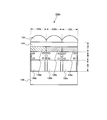
- FIG. 2 shows a cross-sectional structure along the line AB of the pixel portion 102 a shown in the enlarged portion 116.
- FIG. 2 shows a cross-sectional structure of the pixel portion 102a.
- a semiconductor layer 128, a wiring layer 130, an optical filter layer 132, and a microlens array 134 are stacked from the substrate 126 side.
- the pixel portion 102a includes a pixel 122 formed by stacking these layers.
- FIG. 2 shows a mode in which the first pixels 122a to 122c are provided in the pixel portion 102a.
- the first pixels 122a to 122c detect light in different wavelength bands by the optical filter layer 132, respectively.
- the substrate 126 is a semiconductor substrate or a substrate having a semiconductor layer.
- An example of the semiconductor substrate is a silicon substrate, and an example of a substrate having a semiconductor layer is a substrate (SOI substrate) in which a silicon layer is provided over an insulating layer.
- the semiconductor layer 128 is included in the silicon substrate.
- light receiving elements 136a to 136c are formed corresponding to the first pixels 122a to 122c.
- the light receiving elements 136a to 136c are realized by elements having a function of generating current and voltage by the photovoltaic effect.
- the light receiving elements 136a to 136c may be photodiodes, for example.
- a circuit for obtaining detection signals from the light receiving elements 136a to 136c is formed by the semiconductor layer 128 and the wiring layer 130. Yes.
- the wiring layer 130 includes wirings provided in the pixel portion 102a such as address lines and signal lines.
- the wiring layer 130 may be multilayered by separating a plurality of wirings with an interlayer insulating film.
- the address lines and the signal lines extend in the row direction and the column direction and intersect with each other, and thus are provided in different layers with an interlayer insulating film interposed therebetween.
- the optical filter layer 132 includes a plurality of layers having different optical characteristics.
- color filter layers 138 a to 138 c having a transmission band in the visible light wavelength region are provided on the wiring layer 130.
- the color filter layers 138a to 138c are provided so as to overlap the light receiving surfaces of the light receiving elements 136a to 163c, respectively.
- the color filter layers 138a to 138c have different transmission spectra in the visible light wavelength band. That is, each of the color filter layers 138a to 138c has colored layers having different transmission spectra in the visible light wavelength band.
- a cured film 144 is provided on the upper surfaces of the color filter layers 138a to 138c.
- the cured film 144 fills the steps due to the color filter layers 138a to 138c and has a flat upper surface.
- the cured film 144 has a function as a planarizing film, and planarizes the ground of the microlens array 134.
- the microlens array 134 is provided on the upper surface of the cured film 144.
- the microlens array 134 is provided so that each microlens corresponds to the first pixels 122a to 122c.
- the light condensed by each microlens enters the corresponding light receiving elements 136a to 136c.
- the microlens array 134 can be formed using a resin material.
- the microlens array 134 can be produced by processing a resin material applied on the cured film 144, for example.
- the solid-state imaging device 100 has an imaging function by stacking a semiconductor layer 128, a wiring layer 130, an optical filter layer 132, and a microlens array 134 on a substrate 126. Details of the optical filter layer 132 will be described below.
- the color filter layers 138a to 138c are pass filters that transmit visible light in different wavelength bands.
- the color filter layer 138a transmits light in the wavelength band of red light (approximately 610 to 780 nm)
- the color filter layer 138b transmits light in the wavelength band of green light (approximately 500 to 570 nm).
- the layer 138c is a pass filter that can transmit light in a wavelength band of blue light (approximately 430 to 460 nm in wavelength).
- Light transmitted through the color filter layers 138a to 138c is incident on the light receiving elements 136a to 136c, respectively. Therefore, each pixel (first pixel) can be distinguished from the first pixel 122a for detecting red light, the first pixel 122b for detecting green light, and the first pixel 122c for detecting blue light.
- the color filter layers 138a to 138c include at least a first compound that absorbs light in at least a part of the visible light wavelength band and a second compound that has a light absorption peak in the infrared wavelength band.
- the first compound and the second compound are included in at least one of the color filter layer 138a, the color filter layer 138b, and the color filter layer 138c.
- the color filter layer 138a, the color filter layer 138b, and the color filter layer 138c each contain a different first compound.
- at least one or more of the color filter layer 138a, the color filter layer 138b, and the color filter layer 138c contain the second compound.
- the second compound is preferably an infrared absorber that absorbs light in the near infrared wavelength band (for example, 750 to 2500 nm).
- At least one of the color filter layers 138a to 138c includes the second compound together with the specific first compound, transmits light in a specific band in the visible light wavelength band, and absorbs light in the infrared wavelength band. That is, at least one of the color filter layers 138a to 138c has a function as a bandpass filter that transmits a specific visible light band and a function as an infrared cut filter that blocks light in the infrared wavelength band.
- the first compound may be a pigment (pigment or dye) exhibiting light absorption in a specific wavelength band in the visible light band.
- the first compound is not limited to one type of dye, and may be constituted by a plurality of dyes. In this case, the first compound may be regarded as a first compound group that is an assembly of a plurality of kinds of dyes.
- the color filter layers 138a to 138c include first compounds having different light absorption characteristics. Accordingly, each of the first pixels 122a to 122c is a pixel that detects light corresponding to each color.
- the color filter layer 138a is a pass filter that transmits light in the wavelength band of red light so that the first pixel 122a is a red detection pixel
- the color filter layer 138b is a pass filter that transmits light in the wavelength band of green light.
- the first pixel 122b may be a green detection pixel
- the color filter layer 138c may be a pass filter that transmits light in the wavelength band of blue light, whereby the first pixel 122c may be a blue detection pixel.
- Such a first compound can be used without any particular limitation, and the color and material can be appropriately selected according to the use of the color filter. Specific examples include pigments and dyes, and these can be used alone or in combination of two or more.
- CI color index
- Pigment yellow 129 C.I. I. Pigment yellow 138, C.I. I. Pigment yellow 139, C.I. I. Pigment yellow 150, C.I. I. Pigment yellow 179, C.I. I. Pigment yellow 180, C.I. I. Pigment yellow 185, C.I. I. Pigment yellow 211, C.I. I. Yellow pigments such as CI Pigment Yellow 215; C. I. Orange pigments such as CI Pigment Orange 38; C. I. Pigment violet 19, C.I. I. Purple pigment such as CI Pigment Violet 23.
- a brominated diketopyrrolopyrrole pigment represented by the formula (Ic) of JP-T-2011-523433 can also be used as a red pigment.
- lake pigments described in JP-A-2001-081348 can be exemplified.
- the dye is not particularly limited.
- a known dye may be used in addition to a compound classified as a dye in the color index (CI; issued by The Society of Dyeres and Colorists). Can do.
- Such dyes include, for example, xanthene dyes, triarylmethane dyes, cyanine dyes, anthraquinone dyes, azo dyes, dipyrromethene dyes, quinophthalone dyes, coumarin dyes, pyrazolone dyes, quinoline dyes, nitro dyes, from the chromophore structural aspect. And dyes, quinoneimine dyes, phthalocyanine dyes, squarylium dyes, and the like. Also, for example, a dye multimer having a partial structure derived from a dye as described in JP2013-029760A can be used.
- the second compound is a compound having one or more light absorption peaks in an infrared wavelength band having a wavelength of 650 to 2000 nm. Specifically, it is preferable to have a maximum absorption wavelength within a wavelength range of 650 to 2000 nm, more preferably a maximum absorption wavelength within a wavelength range of 700 to 1500 nm, and a maximum absorption within a wavelength range of 750 to 1300 nm. It is more preferable to have a wavelength, and it is particularly preferable to have a maximum absorption wavelength within a wavelength range of 800 to 1200 nm.
- Examples of such second compounds include diiminium compounds, squarylium compounds, cyanine compounds, phthalocyanine compounds, naphthalocyanine compounds, quaterylene compounds, aminium compounds, iminium compounds, azo compounds, and anthraquinone compounds. , At least one selected from the group consisting of a porphyrin compound, a pyrrolopyrrole compound, an oxonol compound, a croconium compound, a hexaphyrin compound, a metal dithiol compound, a copper compound, a metal oxide, a metal boride, and a noble metal Compounds can be used.
- the above-mentioned 2nd compound when the above-mentioned 2nd compound is soluble in the organic solvent mentioned later, it can be raked and it can also be used as an infrared absorber insoluble in an organic solvent.
- a known method can be adopted as the rake method, and for example, JP-A-2007-271745 can be referred to. These can be used alone or in combination of two or more.
- diiminium (diimmonium) compound examples include, for example, JP-A No. 1-113482, JP-A No. 10-180922, International Publication No. 2003/5076, International Publication No. 2004/48480, International Publication No. 2005. No. 4,44782, International Publication No. 2006/120888, Japanese Unexamined Patent Publication No. 2007-246464, International Publication No. 2007/148595, Japanese Unexamined Patent Publication No. 2011-038007, Paragraph [0118] of International Publication No. 2011/118171, etc. And the compounds described.
- EPOLIGHT series such as EPOLIGHT 1178 (manufactured by Epolin)
- CIR-108X series such as CIR-1085 and CIR-96X series (manufactured by Nippon Carlit)
- IRG022, IRG023, PDC-220 Nippon Kayaku
- squarylium compound examples include, for example, Japanese Patent No. 3094037, Japanese Patent Application Laid-Open No. 60-228448, Japanese Patent Application Laid-Open No. 1-146846, Japanese Patent Application Laid-Open No. 1-222896, Japanese Patent Application Laid-Open No. 2012-215806.
- Examples include compounds described in paragraph [0178] of the publication.
- cyanine compound examples include, for example, paragraphs [0041] to [0042] of JP 2007-271745 A, paragraphs [0016] to [0018] of JP 2007-334325 A, and JP 2009-108267 A.
- NK series manufactured by Hayashibara Biochemical Laboratories
- Daito D chmix 1371F manufactured by Daitokemix
- NK-3212 manufactured by Daitokemix
- NK-5060 and the like.
- phthalocyanine compound examples include, for example, JP-A-60-224589, JP-T-2005-537319, JP-A-4-23868, JP-A-4-39361, JP-A-5-78364.
- JP-A 2000-26748, JP-A 2000-63691, JP-A 2001-106689, JP-A 2004-18561, JP-A 2005-220060, JP-A 2007-169343 Examples include compounds described in JP-A-2013-195480, paragraphs [0026] to [0027], Table 1 of International Publication No. 2015/025779, and the like.
- Examples of commercially available products include FB series such as FB-22 and 24 (manufactured by Yamada Chemical Co., Ltd.), Excolor series, Excolor TX-EX 720, 708K (manufactured by Nippon Shokubai), Lumogen IR788 (manufactured by BASF), ABS643, ABS654, ABS667, ABS670T, IRA693N, IRA735 (manufactured by Exciton), SDA3598, SDA6075, SDA8030, SDA8303, SDA8470, SDA3039, SDA3040, SDA3922, SDA7257 (manufactured by H.W.SANDS), TAP-15, IR-15 (Made by industry) etc. can be mentioned.
- FB series such as FB-22 and 24 (manufactured by Yamada Chemical Co., Ltd.)
- Excolor series Excolor TX-EX 720, 708K (manufactured by Nippon Shoku
- naphthalocyanine compounds include, for example, paragraphs [0046] to [0046] in JP-A Nos. 11-152413, 11-152414, 11-152415, and 2009-215542. [0049] and the like.
- quaterrylene compound examples include compounds described in paragraph [0021] of JP-A-2008-009206.
- examples of commercially available products include Lumogen® IR765 (manufactured by BASF).
- aminium compound examples include compounds described in paragraph [0018] of JP-A No. 08-027371, JP-A No. 2007-039343, and the like.
- IRG002, IRG003 made by Nippon Kayaku Co., Ltd.
- IRG003 made by Nippon Kayaku Co., Ltd.
- iminium-based compound examples include compounds described in paragraph [0116] of International Publication No. 2011/118171.
- azo compound examples include compounds described in paragraphs [0114] to [0117] of JP2012-215806A.
- anthraquinone compounds include compounds described in paragraphs [0128] and [0129] of JP 2012-215806 A, for example.
- porphyrin-based compound examples include, for example, a compound represented by the formula (1) in Japanese Patent No. 3834479.
- pyrrolopyrrole compounds include compounds described in paragraphs [0014] to [0027] of JP2011-068731A and JP2014130343A.
- oxonol-based compound examples include compounds described in paragraph [0046] of JP-A-2007-271745.
- croconium-based compound examples include compounds described in paragraph [0049] of JP-A No. 2007-271745, JP-A No. 2007-31644, JP-A No. 2007-169315, and the like.
- hexaphyrin-based compound examples include a compound represented by the formula (1) in International Publication No. 2002/016144 pamphlet.
- metal dithiol compound examples include, for example, JP-A No. 1-114801, JP-A No. 64-74272, JP-A No. 62-39682, JP-A No. 61-80106, and JP-A No. Sho 61-80106.
- examples thereof include compounds described in JP-A 61-42585, JP-A 61-32003, JP-T 2010-516823, and the like.
- Examples of commercially available products include ADS845MC, ADS870MC, ADS920MC (manufactured by American Dye Source, Inc.) and the like.
- Examples of the copper compound include copper metal, copper complex, and copper phosphate.
- a copper complex is preferable, and specific examples thereof include, for example, JP2013-253224A, JP2014-032380A, JP2014-026070A, JP20140261678A, JP2014-139616A. And the compounds described in JP-A No. 2014-139617 and the like.
- Metallic copper can also be used as copper particles.
- Metal oxides include zinc oxide, silicon oxide, aluminum oxide, zirconium dioxide, titanium oxide, cerium dioxide, tungsten oxide, yttrium oxide, indium oxide, tin oxide, and these metal oxides doped with other metals Compounds.
- tungsten oxide is preferable, cesium tungsten oxide and rubidium tungsten oxide are more preferable, and cesium tungsten oxide is more preferable.
- the composition formula of cesium tungsten oxide includes Cs 0.33 WO 3 and the like, and the composition formula of rubidium tungsten oxide includes Rb 0.33 WO 3 and the like.
- the tungsten oxide compound is also available as a dispersion of tungsten fine particles such as YMF-02A manufactured by Sumitomo Metal Mining Co., Ltd.
- metal oxides doped with other metals include ITO (indium oxide doped with tin), ATO (tin oxide doped with antimony), AZO (zinc oxide doped with antimony), and the like. These are preferably in the form of particles of 1 to 1000 nm, more preferably 1 to 100 nm.
- metal boride examples include compounds described in paragraph [0049] of JP 2012-068418 A, for example. Among these, lanthanum boride is preferable.
- noble metal examples include gold, silver, platinum, palladium, rhodium, iridium, ruthenium and osmium, and gold, silver and palladium are particularly preferable. These are preferably particulate or colloidal.
- the second compound contains a metal atom-containing compound from the viewpoint of forming a color filter layer having excellent light blocking performance and heat resistance in the infrared wavelength band.
- the metal atom-containing compound preferably contains at least one compound selected from a metal phthalocyanine compound, a metal porphyrin compound, a metal dithiol compound, a copper compound, a metal oxide, a metal boride, a noble metal, and a lake pigment, More preferably, it contains at least one compound selected from metal oxides.
- a compound having a condensed ring is also preferable. By using such a compound, a color filter layer having excellent heat resistance can be formed.
- compounds having a condensed ring it is preferable to include at least one compound selected from a quaterylene compound, an anthraquinone compound, a pyrrolopyrrole compound, a croconium compound, and a perylene compound.
- the content ratio of the second compound per unit volume is preferably 0.1 to 60% by mass.
- the content of the second compound is preferably 10 to 300 parts by mass, more preferably 20 to 200 parts by mass with respect to 100 parts by mass of the first compound.
- the color filter layers 138a to 138c are produced using a curable composition containing the first compound.
- the color filter layers 138a to 138c are manufactured using a curable composition including the first compound and the second compound.
- the curable composition for producing the color filter layer is based on a binder resin, a curing agent, and the like, and includes the first compound or the first compound and the second compound. By using such a curable composition, the color filter layers 138a to 138c can be provided above the light receiving elements 136a to 136c.
- the curable composition for producing the color filter layers 138a to 138c may be a positive radiation sensitive composition further containing a photosensitizing agent and a curing agent in addition to the above composition.
- the negative radiation sensitive composition containing binder resin, a polymeric compound, and a photosensitive agent may be sufficient.
- the negative radiation-sensitive composition preferably contains a first compound, a binder resin, a polymerizable compound, and a photosensitizer, and may further contain a second compound, a solvent, an additive, and the like as necessary.
- the binder resin in the negative radiation sensitive composition is preferably a (meth) acrylic polymer having an acidic functional group such as a carboxyl group or a phenolic hydroxyl group.
- Preferred examples of the (meth) acrylic polymer having a carboxyl group include an ethylenically unsaturated monomer having one or more carboxyl groups. (Hereinafter also referred to as “unsaturated monomer (1)”) and other copolymerizable ethylenically unsaturated monomers (hereinafter also referred to as “unsaturated monomer (2)”). Can be mentioned.
- Examples of the unsaturated monomer (1) include (meth) acrylic acid, maleic acid, maleic anhydride, succinic acid mono [2- (meth) acryloyloxyethyl], ⁇ -carboxypolycaprolactone mono (meta ) Acrylate, p-vinylbenzoic acid and the like.
- Examples of the unsaturated monomer (2) include N-substituted maleimides, aromatic vinyl compounds, (meth) acrylic acid esters, vinyl ethers, and mono (meth) acryloyl groups at the ends of polymer molecular chains. And more specifically, monomers described in JP-A-2015-004968, [0060] to [0062].
- These unsaturated monomers (1) to (2) can be used alone or in combination of two or more.
- copolymer of the unsaturated monomer (1) and the unsaturated monomer (2) include, for example, JP-A-7-140654, JP-A-8-259876, and JP-A-10-31308. No. 10, JP-A-10-300902, JP-A-11-174224, JP-A-11-258415, JP-A-2000-56118, JP-A-2004-101728, etc. Coalescence can be mentioned.
- a carboxyl group-containing (meth) acrylic polymer having a polymerizable unsaturated bond such as a (meth) acryloyl group in the side chain can also be used as a binder resin.
- the (meth) acrylic polymer in the present invention has a polystyrene-equivalent weight average molecular weight (Mw) measured by gel permeation chromatography (hereinafter abbreviated as GPC) (elution solvent: tetrahydrofuran) usually from 1,000 to 1,000. 100,000, preferably 3,000 to 50,000.
- GPC gel permeation chromatography
- the ratio (Mw / Mn) of the weight average molecular weight (Mw) to the number average molecular weight (Mn) of the (meth) acrylic polymer in the present invention is preferably 1.0 to 5.0, more preferably 1.0 to 3.0.
- Mn here says the number average molecular weight of polystyrene conversion measured by GPC (elution solvent: tetrahydrofuran).
- the (meth) acrylic polymer in the present invention can be produced by a known method.
- the structure, Mw, and Mw / Mn can also be controlled by the method disclosed in FIG.
- a siloxane polymer can also be preferably used as the binder resin in the negative radiation sensitive composition. Although it does not specifically limit as a siloxane polymer, The siloxane polymer which has an aromatic hydrocarbon group is preferable.
- the “aromatic hydrocarbon group” refers to a hydrocarbon group having an aromatic ring structure in the ring structure, and a monocyclic aromatic hydrocarbon group, benzene rings are condensed with each other or a benzene ring.
- the aromatic hydrocarbon group does not need to be composed only of a ring structure, and a part of the ring structure may be substituted with a chain hydrocarbon group.
- the number of carbon atoms of the aromatic hydrocarbon group is not particularly limited, but is preferably 6 to 20, more preferably 6 to 14, and still more preferably 6 to 10.
- aromatic hydrocarbon group examples include, for example, phenyl group, tolyl group, xylyl group, mesityl group, styryl group, indenyl group, naphthyl group, anthryl group, phenanthryl group, fluorenyl group, pyrenyl group, naphthaacenaphthenyl. Group, biphenyl group, terphenyl group and the like. Among them, an aromatic hydrocarbon group having 6 to 14 carbon atoms is preferable, an aryl group having 6 to 14 carbon atoms is more preferable, and a phenyl group, a tolyl group, and a naphthyl group are further preferable.
- the “aryl group” refers to a monocyclic to tricyclic aromatic hydrocarbon group.
- aromatic hydrocarbon group may have a substituent.
- the content of aromatic hydrocarbon groups with respect to Si atoms is preferably 5 mol% or more, more preferably 20 mol% or more, and more preferably 60 mol% or more. Further preferred.
- the content rate with respect to Si atom of this aromatic hydrocarbon group may be 100 mol%, it is good also as 95 mol% or less.
- Such a siloxane polymer can be obtained by hydrolytic condensation of at least one selected from a silane compound having an aromatic hydrocarbon group and a hydrolyzable group and a partial hydrolyzate thereof, specifically, It can be synthesized by a known method.
- the siloxane polymer in the present invention has a weight average molecular weight (Mw) of preferably 500 to 10,000, more preferably 700 to 5,000.
- the ratio (Mw / Mn) of the weight average molecular weight (Mw) to the number average molecular weight (Mn) is preferably 1.0 to 5.0, more preferably 1.0 to 3.0.
- the binder resin can be used alone or in combination of two or more.
- the content of the binder resin is usually 10 to 1,000 parts by mass, preferably 20 to 500 parts by mass, and more preferably 50 to 200 parts by mass with respect to 100 parts by mass of the first compound. Further, the content of the polymerizable compound with respect to 100 parts by mass of the binder resin is preferably 20 to 500 parts, and more preferably 50 to 200 parts by mass.
- the polymerizable compound in the negative radiation-sensitive composition refers to a compound having two or more polymerizable groups.
- the polymerizable group include an ethylenically unsaturated group, an oxiranyl group, an oxetanyl group, an N-alkoxymethylamino group, a silanol group, and a methylol group.
- the polymerizable compound includes a compound having two or more (meth) acryloyl groups, a compound having two or more N-alkoxymethylamino groups, a compound having two or more silanol groups, A compound having the above methylol group is preferred.
- the compound having two or more (meth) acryloyl groups include a polyfunctional (meth) acrylate obtained by reacting an aliphatic polyhydroxy compound and (meth) acrylic acid, a polyfunctional (meta) modified with caprolactone. ) Acrylate, alkylene oxide modified polyfunctional (meth) acrylate, polyfunctional urethane (meth) acrylate obtained by reacting hydroxyl-functional (meth) acrylate and polyfunctional isocyanate, hydroxyl-functional (meth) acrylate and acid anhydride
- the polyfunctional (meth) acrylate which has a carboxyl group obtained by making a product react can be mentioned.
- a polyfunctional (meth) acrylate obtained by reacting an aliphatic polyhydroxy compound and (meth) acrylic acid described in [0073] of JP-A-2015-004968, or JP-A-2015 Examples thereof include polymerizable compounds described in [0074] to [0075] of JP-A-004968.
- the polymerizable compounds can be used alone or in combination of two or more.
- the content of the polymerizable compound in the present invention is preferably 10 to 1,000 parts by mass, more preferably 20 to 500 parts by mass, and still more preferably 30 to 300 parts by mass with respect to 100 parts by mass of the first compound.
- the negative radiation-sensitive composition of the present invention can contain a photosensitizer. Thereby, radiation sensitivity can be provided to a negative radiation sensitive composition.
- the photosensitive agent used in the present invention is a compound that generates active species capable of initiating polymerization of the polymerizable compound by exposure to radiation such as visible light, ultraviolet light, far ultraviolet light, electron beam, and X-ray.
- Examples of such a photosensitizer include a radical polymerization initiator and a photoacid generator.
- radical polymerization initiators include thioxanthone compounds, acetophenone compounds, biimidazole compounds, triazine compounds, O-acyloxime compounds, onium salt compounds, benzoin compounds, benzophenone compounds, ⁇ -diketone compounds, polynuclear quinone compounds, diazo compounds, Examples thereof include imidosulfonate compounds. More specifically, compounds described in [0081] to [0087] of JP-A-2015-004968 can be mentioned.
- radical polymerization initiators at least one selected from the group of thioxanthone compounds, acetophenone compounds, biimidazole compounds, triazine compounds, and O-acyloxime compounds is preferable.
- the photoacid generator include those described in JP-A-2011-068755, [0024].
- the photosensitive agent can be used alone or in combination of two or more.
- the content of the photosensitizer is preferably 0.01 to 120 parts by weight, more preferably 1 to 100 parts by weight, and still more preferably 5 to 50 parts by weight with respect to 100 parts by weight of the polymerizable compound.
- the negative radiation-sensitive composition is usually prepared as a liquid composition by blending a solvent.
- a solvent as long as it disperses or dissolves the components constituting the negative radiation-sensitive composition and does not react with these components and has appropriate volatility, it can be appropriately selected and used. it can.
- solvents examples include those described in JP-A-2015-004968, [0090] to [0093].
- the solvents may be used alone or in admixture of two or more.
- the content of the solvent is not particularly limited, but is preferably such that the total concentration of each component excluding the solvent of the negative radiation-sensitive composition is 5 to 50% by mass, and 10 to 30% by mass. Is more preferred.
- additives such as fillers, surfactants, adhesion promoters, antioxidants, ultraviolet absorbers, anti-aggregation agents, residue improvers, developability improvers, etc. may be added to the negative radiation sensitive composition. It can. Examples of such additives include those described in JP-A-2015-004968, [0097].
- the positive radiation-sensitive composition preferably contains a first compound, a photosensitizer, and a curing agent, and may further contain a second compound, a binder resin, a solvent, an additive, and the like as necessary.
- Examples of the photosensitive agent in the positive radiation sensitive composition include a compound having a naphthoquinone diazide group and a photoacid generator.
- a compound having a naphthoquinone diazide group for example, an ester of a phenol compound and a naphthoquinone diazide sulfonic acid compound can be used.
- the phenol compound include bi- to 5-functional hydroxybenzophenones, compounds represented by the following formulas (2) to (6) (wherein R in the formula (6) represents a hydrogen atom), and the like.
- Examples of the naphthoquinone diazide sulfonic acid compound include o-naphthoquinone diazide-5-sulfonic acid and o-naphthoquinone diazide-4-sulfonic acid.
- Examples of the photoacid generator are the same as those described above.
- a compound having two or more N-alkoxymethylamino groups is preferable. Specifically, N, N, N ′, N ′, N ′′, N ′′ -hexa (alkoxymethyl) melamine, N, N, N ′, N′-tetra (alkoxymethyl) benzoguanamine, N, N , N ′, N′-tetra (alkoxymethyl) glycoluril and the like.
- binder resin, solvent, and additive in the positive radiation sensitive composition examples include the same binder resin, solvent, and additive as in the negative radiation sensitive composition.
- a cured film 144 may be provided between the color filter layers 138a to 138c and the microlens array 134.
- the cured film 144 preferably has a light-transmitting property with respect to at least light in the visible light wavelength region. The light incident through the microlens array 134 passes through the cured film 144, and the light dispersed by the color filter layers 138a to 138c enters the light receiving elements 136a to 136c.
- the cured film 144 preferably has an insulating property so that no parasitic capacitance is generated between the cured film 144 and the wiring layer 130. Since the cured film 144 is provided on the front surface of the optical filter layer 132, if the cured film 144 is conductive, an unintended parasitic capacitance is generated between the wiring layer 130 and the cured film 144. When the parasitic capacitance is generated, the detection operation of the light receiving elements 136a to 136c is hindered. Therefore, the cured film 144 preferably has an insulating property.
- the cured film 144 is excellent in adhesion with the base layer. For example, if the adhesiveness between the cured film 144 and the color filter layers 138a to 138c is poor, peeling occurs and the optical filter layer 132 is damaged.
- the cured film 144 has a flat surface in order to embed the color filter layers 138a to 138c and provide the microlens array 134 thereon. That is, the cured film 144 is preferably used as a planarizing film.
- the cured film 144 is preferably an organic film. If an organic film is used, it has translucency and insulating properties, and the surface can be flattened. That is, by using a curable composition for forming a planarization film as the cured film 144, a level surface after application of the composition can form a flat surface even if the ground surface includes irregularities. .
- a known curable composition can be used, and a known method can be adopted as a method of forming the cured film.
- the color filter layer can be protected by such a cured film, and the ground plane of the microlens array can be flattened by such a cured film.
- the thickness of the optical filter is reduced by adding a function of absorbing light in the infrared band to the color filter layer that selectively transmits light in the visible light band. Therefore, it is possible to reduce the size of the solid-state imaging device.
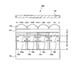
- FIG. 3 shows a cross-sectional structure of the pixel portion 102b of the solid-state imaging device according to this embodiment.
- the pixel portion 102b is the same as that of the first embodiment in that the semiconductor layer 128, the wiring layer 130, the optical filter layer 132, and the microlens array 134 are included in the layer structure.
- the pixel portion 102b of the solid-state imaging device according to the present embodiment has a back-illuminated configuration in which the wiring layer 130 is disposed on the lower surface side of the light receiving elements 136a to 136c.
- the back-illuminated pixel portion is formed of thin pieces so that after the light receiving elements 136a to 136c and the wiring layer 130 are formed on the semiconductor substrate, the back surface of the semiconductor substrate is ground and polished to expose the light receiving elements 136a to 136c. It has become.
- the substrate 126 is attached to the wiring layer 130 as a supporting base material.
- the back-illuminated pixel portion 102b does not have the wiring layer 130 on the light receiving surfaces of the light receiving elements 136a to 136c, a wide aperture ratio can be obtained, loss of incident light can be suppressed, and a bright image can be output even with the same amount of light. There are advantages.
- the configuration of the optical filter layer 132 and the microlens array 134 is the same as that of the first embodiment.
- An organic film 146 is provided between the light receiving elements 136a to 136c and the color filter layers 138a to 138c.
- the organic film 146 covers the upper surfaces of the light receiving elements 136a to 136c and flattens the lower ground of the color filter layers 138a to 138c. It also functions as a protective film for the light receiving elements 136a to 136c.
- the organic film 146 is produced using the same curable composition as the composition for producing the cured film 144 shown in the first embodiment. If these materials are used, the upper surfaces of the light receiving elements 136a to 136c can be planarized.
- the pixel unit 102b is a back-illuminated type, so that the light use efficiency is improved and a highly sensitive solid-state imaging device is provided.
- the optical filter layer 132 has the same configuration as that of the first embodiment, the optical filter layer is thinned, and the solid-state imaging device can be thinned. That is, according to the present embodiment, it is possible to provide a solid-state imaging device that has the same effects as those of the first embodiment while having a back-illuminated feature.
- FIG. 4 shows a cross-sectional structure of the pixel portion 102c of the solid-state imaging device according to this embodiment.
- the pixel portion 102c includes an infrared light detection pixel formed by the second pixel 124 in addition to a visible light detection pixel formed by the first pixels 122a to 122c. Except for including the second pixel 124, it has the same configuration as the pixel shown in the first embodiment. That is, the pixel portion 102 c is configured by the semiconductor layer 128, the wiring layer 130, the optical filter layer 132, and the microlens array 134.
- a near-infrared pass filter layer 140 is provided on the light receiving surface side of the light receiving element 136d.
- a microlens array 134 is provided above the near infrared pass filter layer 140.
- the near infrared pass filter layer 140 is a pass filter that transmits at least light in the near infrared wavelength region.
- the near-infrared pass filter layer 140 can be formed by adding a pigment (pigment or dye) having absorption at a wavelength in the visible light wavelength region to a binder resin or a polymerizable compound.
- the near-infrared pass filter layer 140 absorbs (cuts) light having a wavelength of generally less than 700 nm, preferably less than 750 nm, more preferably less than 800 nm, and transmits light having a wavelength of 700 nm or more, preferably 750 nm or more, more preferably 800 nm or more. It has spectral transmission characteristics.
- the near-infrared pass filter layer 140 blocks light having a wavelength less than a predetermined wavelength (for example, less than 750 nm) as described above, and transmits near-infrared light in a predetermined wavelength region (for example, 750 nm or more, for example, 750 to 950 nm).
- a near infrared ray is incident on the light receiving element 136d.
- the light receiving element 136d can detect infrared rays with high accuracy without being affected by noise or the like caused by visible light.
- the second pixel 122d and the second pixel 124 can be used as an infrared detection pixel.
- the near-infrared pass filter layer 140 can be formed using, for example, a photosensitive composition described in JP-A-2014-130332.
- the solid-state imaging device can juxtapose the pixels that detect the visible light wavelength band and the pixels that detect the infrared wavelength band without adding a new optical filter.
- the upper surfaces of the color filter layers 138a to 138c and the upper surface of the near-infrared pass filter layer 140 are provided so that the heights thereof substantially coincide.
- the cured film 144 can have a function as a planarizing film by itself, but when the cured film 144 is formed by applying a known curable composition, the closer the base surface is to the flat, The uneven coating of the curable composition can be reduced, and the flatness of the upper surface of the cured film 144 can be improved.
- the microlens array 134 formed on the upper surface of the cured film 144 can be molded with high accuracy, and the solid-state imaging device can acquire an image with little distortion.
- the solid-state imaging device may be provided with a two-band pass filter 148 on the microlens array 134 in addition to the above configuration. That is, on the upper surface of the microlens array 134, for example, the average transmittance in the wavelength range of 430 to 580 nm is 75% or more, the average transmittance in the wavelength range of 720 to 750 nm is 15% or less, and the average in the range of wavelengths 810 to 820 nm.
- a two-band pass filter 148 having a transmittance of 60% or more and an average transmittance of 15% or less in the wavelength range of 900 to 2000 nm may be provided. By adding the two-band pass filter 148, the filtering ability in the visible light wavelength region and the infrared wavelength region can be further enhanced.
- the light incident through the microlens array 134 is split into visible light in each band by the color filter layers 138a to 138c in the first pixels 122a to 122c.
- the light in the infrared wavelength band is cut and incident on the light receiving elements 136a to 136c.
- the second pixel 124 is incident on the near-infrared pass filter layer 140 as it is.
- the first pixels 122a to 122c visible rays filtered by the color filter layers 138a to 138c are incident on the light receiving elements 136a to 136c, respectively.
- One or more of the color filter layers 138a to 138c have the property of cutting infrared rays, so that visible light can be detected with high accuracy without being affected by noise caused by infrared rays.
- the second pixel 124 the light in the visible light wavelength region is cut by the near infrared pass filter layer 140, and the light in the infrared wavelength region (particularly, the near infrared wavelength region) is incident on the light receiving element 136d. Thereby, infrared rays can be detected with high accuracy without being affected by noise or the like caused by visible light.
- the solid-state imaging device can realize a solid-state imaging device capable of ranging by the TOF method by integrally providing a visible light detection pixel and an infrared light detection pixel. That is, the image data of the subject can be acquired with the visible light detection pixel, and the distance to the subject can be measured with the infrared light detection pixel. Thereby, three-dimensional image data can be acquired. In this case, in the visible light detection pixel, light in the infrared wavelength region is blocked, and high-sensitivity imaging with less noise can be performed. In the infrared detection pixel, light in the visible light wavelength region is blocked, and high-precision distance measurement can be performed.
- the function of cutting light in the infrared wavelength band is added to the color filter layers 138a to 138c, so that the optical filter layer 132 is thinned, and the solid-state imaging device is thinned. Can be achieved. Thereby, it can contribute to thickness reduction of the housing
- the configuration of the pixel portion 102c in the present embodiment is the same as that of the first pixel except that a second pixel 124 that detects light in the infrared wavelength band is added to the first pixels 122a to 122c that detect light in the visible light band. This is the same as the embodiment. That is, according to the present embodiment, in addition to the above features, it is possible to provide a solid-state imaging device that exhibits the same operational effects as the first embodiment.
- the obtained binder resin (B-1) had an Mw of 9,700 and an Mn of 5,700.
- This block copolymer is referred to as “dispersant (X-1)”.
- C.I. I. Pigment Green 58 is added in an amount of 7.5 parts by mass and C.I. I. 7.5 parts by weight of Pigment Yellow 139, 11.25 parts by weight of a dispersant (X-1) solution (solid content concentration of 40% by mass) as a dispersant, and a binder resin (B-1) solution (solid content concentration of 40 masses) %) was processed by a bead mill using 13.75 parts by mass of PGMEA as a solvent and a pigment dispersion (A-1) was prepared.
- X-1 solution solid content concentration of 40% by mass
- B-1 solution solid content concentration of 40 masses
- this resin solution was diluted with 33.3 parts by mass (containing 10 parts of polymer), methyl-3-methoxypropionate with 31.9 parts by mass, and propylene glycol monomethyl ether with 3.4 parts by mass.
- 0.3 parts by mass of trimellitic acid, 0.5 parts by mass of 3-glycidoxypropyltrimethoxysilane, and 0.005 parts by mass of the product name “FC-4432” (manufactured by Sumitomo 3M Limited) were dissolved. Then, a composition for forming a base film was prepared.
- Example 1 40.54 parts by mass of YMF-02A (manufactured by Sumitomo Metal Mining Co., Ltd., 18.5% by mass dispersion of cesium tungsten oxide (Cs 0.33 WO 3 , average dispersed particle size 800 nm or less)) as an infrared shielding material, and A colorant dispersion was prepared by mixing 33.33 parts by mass of the pigment dispersion (A-1).
- YMF-02A manufactured by Sumitomo Metal Mining Co., Ltd., 18.5% by mass dispersion of cesium tungsten oxide (Cs 0.33 WO 3 , average dispersed particle size 800 nm or less)
- a colorant dispersion was prepared by mixing 33.33 parts by mass of the pigment dispersion (A-1).
- the solid content concentration in the negative radiation-sensitive composition (S-1) is 24.5% by mass, and the content of the polymerizable compound with respect to 100 parts by mass of the binder resin is 73 parts by mass. Moreover, the content rate of an infrared shielding material and a coloring agent is 7.5 / 5.0 (mass ratio).
- a negative radiation sensitive composition (S-1) was applied on this undercoat film by spin coating, and then prebaked at 100 ° C. for 120 seconds to form a coating film having a thickness of 2.0 ⁇ m.
- the green cured film pattern had a maximum transmission wavelength in the wavelength region of 500 to 600 nm, and the transmittance at the maximum transmission wavelength was 60% or more.
- the maximum transmittance in the wavelength region of 750 to 800 nm was more than 10% and not more than 30%, and the maximum transmittance in the wavelength region of 800 to 1200 nm was also more than 10% and not more than 30%. Further, even after this green cured film pattern was additionally post-baked at 230 ° C. for 10 minutes, the minimum transmittance was 30% or less in a part of the wavelength region of 750 to 1200 nm.
- the color filter layer having the green cured film pattern as a green pixel is excellent in the transmittance in the green region and has a reduced transmittance in the infrared wavelength band.
- the solid-state imaging device provided can reduce the thickness of the optical filter, and thus it can be said that the solid-state imaging device can be miniaturized.
- Example 2 In Example 1, the negative radiation-sensitive composition (S-2) was prepared in the same manner as in Example 1 except that the pigment dispersion (A-2) was used instead of the pigment dispersion (A-1). Prepared.
- Example 1 blue curing was performed in the same manner as in Example 1 except that the negative radiation sensitive composition (S-2) was used instead of the negative radiation sensitive composition (S-1). A film pattern was formed.
- the blue cured film pattern had a maximum transmission wavelength in the wavelength region of 400 to 500 nm, and the transmittance at the maximum transmission wavelength was 60% or more.
- the maximum transmittance in the wavelength region of 750 to 800 nm was more than 10% and not more than 30%, and the maximum transmittance in the wavelength region of 800 to 1200 nm was also more than 10% and not more than 30%. Further, even after this blue cured film pattern was additionally post-baked at 230 ° C. for 10 minutes, the minimum transmittance was 30% or less in a part of the wavelength region of 750 to 1200 nm.
- the color filter layer having the blue cured film pattern as a blue pixel has excellent transmittance in the blue region and the transmittance in the infrared wavelength band is reduced.
- the solid-state imaging device provided can reduce the thickness of the optical filter, and thus it can be said that the solid-state imaging device can be miniaturized.
- Example 1 green curing was performed in the same manner as in Example 1 except that the negative radiation sensitive composition (S-3) was used instead of the negative radiation sensitive composition (S-1). A film pattern was formed.
- This green cured film pattern had a maximum transmission wavelength in the wavelength region of 500 to 600 nm, and the transmittance at the maximum transmission wavelength was 60% or more.
- the maximum transmittance in the wavelength region of 750 to 800 nm is 30% or more and 50% or less
- the maximum transmittance in the wavelength region of 800 to 1200 nm is 50% or more. From this, the color filter layer having the green cured film pattern as a green pixel is excellent in the transmittance in the green region, but it cannot be said that the transmittance in the infrared wavelength band is reduced. It can be said that miniaturization is difficult.
- Comparative Example 2 In Comparative Example 1, a negative radiation-sensitive composition (S-4) was prepared in the same manner as in Comparative Example 1, except that the pigment dispersion (A-2) was used instead of the pigment dispersion (A-1). Prepared.
- Example 1 blue curing was performed in the same manner as in Example 1 except that the negative radiation sensitive composition (S-4) was used instead of the negative radiation sensitive composition (S-1). A film pattern was formed.
- This blue cured film pattern had a maximum transmission wavelength in the wavelength region of 400 to 500 nm, and the transmittance at the maximum transmission wavelength was 60% or more.
- the maximum transmittance in the wavelength region of 750 to 800 nm is 30% or more and 50% or less
- the maximum transmittance in the wavelength region of 800 to 1200 nm is 50% or more. From this, the color filter layer having the blue cured film pattern as a blue pixel is excellent in the transmittance in the blue region, but it cannot be said that the transmittance in the infrared wavelength band is reduced. It can be said that miniaturization is difficult.
- Example 3 In Example 1, instead of 40.54 parts by mass of YMF-02A, a 5% by mass cyclohexanone solution of compound (a-12) (phthalocyanine compound in which the central metal is vanadium) described in International Publication No. 2015/025779. A negative radiation-sensitive composition (S-5) was prepared in the same manner as in Example 1 except that 20 parts by mass was used.
- compound (a-12) phthalocyanine compound in which the central metal is vanadium
- Example 1 green curing was performed in the same manner as in Example 1 except that the negative radiation sensitive composition (S-5) was used instead of the negative radiation sensitive composition (S-1). A film pattern was formed.
- the green cured film pattern had a maximum transmission wavelength in the wavelength region of 500 to 600 nm, and the transmittance at the maximum transmission wavelength was 60% or more.
- the maximum transmittance in the wavelength region of 750 to 800 nm was more than 10% and not more than 30%, but the maximum transmittance in the wavelength region of 800 to 1200 nm was more than 50%. Further, even after this green cured film pattern was additionally post-baked at 230 ° C. for 10 minutes, the minimum transmittance was 30% or less in a part of the wavelength region of 750 to 800 nm.
- the color filter layer having the green cured film pattern as a green pixel has excellent transmittance in the green region and has reduced transmittance in the infrared wavelength band of 750 to 800 nm.
- the solid-state imaging device including the color filter layer can reduce the thickness of the optical filter, and thus it can be said that the solid-state imaging device can be reduced in size.
- Example 4 In Preparation Example 2, C.I. I. Pigment Blue 15: 6 12 parts by mass and C.I. I. Instead of 3 parts by mass of Pigment Violet 23, a salt-forming compound (cyanine-based compound) of “Dye-E” and K 6 (P 2 MoW 17 O 62 ) described in JP 2011-225761 A is obtained.
- the pigment dispersion (A-3) was prepared in the same manner as in Preparation Example 2 except that 15 parts by mass of a cationic cyanine chromophore and an anion having a molybdenum atom and a tungsten atom) was used.
- a negative radiation sensitive composition (S) was prepared in the same manner as in Example 1 except that the pigment dispersion (A-3) was used instead of 40.54 parts by mass of YMF-02A. -6) was prepared.
- Example 1 green curing was performed in the same manner as in Example 1 except that the negative radiation sensitive composition (S-6) was used instead of the negative radiation sensitive composition (S-1). A film pattern was formed.
- the green cured film pattern had a maximum transmission wavelength in the wavelength region of 500 to 600 nm, and the transmittance at the maximum transmission wavelength was 60% or more.
- the maximum transmittance in the wavelength region of 750 to 800 nm was more than 10% and not more than 30%, but the maximum transmittance in the wavelength region of 800 to 1200 nm was more than 50%. Further, even after this green cured film pattern was additionally post-baked at 230 ° C. for 10 minutes, the minimum transmittance was 30% or less in a part of the wavelength region of 750 to 800 nm.
- the color filter layer having the green cured film pattern as a green pixel has excellent transmittance in the green region and has reduced transmittance in the infrared wavelength band of 750 to 800 nm.
- the solid-state imaging device including the color filter layer can reduce the thickness of the optical filter, and thus it can be said that the solid-state imaging device can be reduced in size.
- Example 1 is the same as Example 1 except that instead of 40.54 parts by mass of YMF-02A, 46.55 parts by mass of a 10% by mass cyclohexanone solution of ADS870MC (manufactured by American Dye Source), which is a nickel dithiol compound, was used. Similarly, a negative radiation sensitive composition (S-7) was prepared.
- ADS870MC manufactured by American Dye Source
- Example 1 green curing was performed in the same manner as in Example 1 except that the negative radiation sensitive composition (S-7) was used instead of the negative radiation sensitive composition (S-1). A film pattern was formed.
- the green cured film pattern had a maximum transmission wavelength in the wavelength region of 500 to 600 nm, and the transmittance at the maximum transmission wavelength was 60% or more.
- the maximum transmittance in the wavelength region of 750 to 800 nm was more than 10% and not more than 30%, but the maximum transmittance in the wavelength region of 800 to 1200 nm was more than 50%. Further, even after this green cured film pattern was additionally post-baked at 230 ° C. for 10 minutes, the minimum transmittance was 30% or less in a part of the wavelength region of 750 to 800 nm.
- the color filter layer having the green cured film pattern as a green pixel has excellent transmittance in the green region and has reduced transmittance in the infrared wavelength band of 750 to 800 nm.
- the solid-state imaging device including the color filter layer can reduce the thickness of the optical filter, and thus it can be said that the solid-state imaging device can be reduced in size.
- Example 6 In Example 1, except that 12.25 parts by mass of a 5 mass% cyclohexanone solution of the compound (a-12) (phthalocyanine-based compound whose central metal is vanadium) of International Publication No. 2015/025779 was further added as an infrared shielding material. Prepared a negative radiation-sensitive composition (S-8) in the same manner as in Example 1.
- Example 1 green curing was performed in the same manner as in Example 1 except that the negative radiation sensitive composition (S-8) was used instead of the negative radiation sensitive composition (S-1). A film pattern was formed.
- the green cured film pattern had a maximum transmission wavelength in the wavelength region of 500 to 600 nm, and the transmittance at the maximum transmission wavelength was 60% or more. Further, the maximum transmittance in the wavelength region of 750 to 800 nm was 10% or less, and the maximum transmittance in the wavelength region of 800 to 1200 nm was 10% or less. Further, even after this green cured film pattern was additionally post-baked at 230 ° C. for 10 minutes, the minimum transmittance was 30% or less in a part of the wavelength region of 750 to 1200 nm.
- the color filter layer having the green cured film pattern as a green pixel is excellent in the transmittance of the green region and the transmittance in the infrared wavelength band is extremely reduced. Therefore, it can be said that the thickness of the optical filter can be reduced, and thus the solid-state imaging device can be reduced in size.
- Example 1 was used except that instead of 40.54 parts by mass of YMF-02A in Example 1, 24.50 parts by mass of a 2% by mass cyclohexanone solution of a squarylium compound represented by the following formula (a-3) was used. In the same manner as described above, a negative radiation-sensitive composition (S-9) was prepared.
- Example 1 green curing was performed in the same manner as in Example 1 except that the negative radiation sensitive composition (S-9) was used instead of the negative radiation sensitive composition (S-1). A film pattern was formed.
- This green cured film pattern had a maximum transmission wavelength in the wavelength region of 500 to 600 nm, and the transmittance at the maximum transmission wavelength was 60% or more.
- the maximum transmittance in the wavelength region of 750 to 800 nm was more than 10% and not more than 30%, but the maximum transmittance in the wavelength region of 800 to 1200 nm was more than 50%.
- this green cured film pattern was subjected to additional post-baking at 230 ° C. for 10 minutes, the minimum transmittance in the wavelength region of 750 to 800 nm was more than 30%.
- the color filter layer having the green cured film pattern as a green pixel is excellent in the transmittance in the green region, but it cannot be said that the transmittance in the infrared wavelength band is reduced. It can be said that miniaturization is difficult.
- DESCRIPTION OF SYMBOLS 100 Solid-state imaging device, 102 ... Pixel part, 104 ... Vertical selection circuit, 106 ... Horizontal selection circuit, 108 ... Sample hold circuit, 110 ... Amplification circuit, 112 ... A / D conversion circuit, 114 ... timing generation circuit, 116 ... enlargement unit, 122 ... first pixel, 124 ... second pixel, 126 ... substrate, 128 ... semiconductor layer, 130 ... Wiring layer, 132 ... Optical filter layer, 134 ... Microlens array, 136 ... Photodiode, 138 ... Color filter layer, 140 ... Near infrared pass filter layer, 144 ..Curing films, 146 ... organic films, 148 ... two band pass filters
Landscapes
- Physics & Mathematics (AREA)
- Engineering & Computer Science (AREA)
- Power Engineering (AREA)
- General Physics & Mathematics (AREA)
- Electromagnetism (AREA)
- Condensed Matter Physics & Semiconductors (AREA)
- Computer Hardware Design (AREA)
- Microelectronics & Electronic Packaging (AREA)
- Optics & Photonics (AREA)
- Signal Processing (AREA)
- Multimedia (AREA)
- Solid State Image Pick-Up Elements (AREA)
- Optical Filters (AREA)
- Materials For Photolithography (AREA)
Abstract
Description
<固体撮像装置の構造>
図1は、本実施形態に係る固体撮像装置100の一例を示す概略構成図を示す。固体撮像装置100は、画素部102、垂直選択回路104、水平選択回路106、サンプルホールド回路108、増幅回路110、A/D変換回路112、タイミング発生回路114等が含まれている。画素部102及び画素部102に付随して設けられる各種機能回路は同一の基板(半導体チップ)に設けられていてもよい。画素部102は、複数の画素122を含み、CMOS型イメージセンサ又はCCD型イメージセンサによって構成されている。
図2は、画素部102aの断面構造を示す。画素部102aは、基板126側から、半導体層128、配線層130、光学フィルタ層132、マイクロレンズアレイ134が積層されている。画素部102aは、これら各層が積層されて形成される画素122を有している。図2は、画素部102aにおいて、第1画素122a~122cが設けられる態様を示す。第1画素122a~122cは、光学フィルタ層132により、それぞれが異なる波長帯域の光を検出する。
カラーフィルタ層138a~138cは、それぞれ異なる波長帯域の可視光線を透過するパスフィルタである。例えば、カラーフィルタ層138aは赤色光(概ね波長610~780nm)の波長帯域の光を透過し、カラーフィルタ層138bは緑色光(概ね波長500~570nm)の波長帯域の光を透過し、カラーフィルタ層138cは青色光(概ね波長430~460nm)の波長帯域の光を透過することができるパスフィルタである。受光素子136a~136cには、それぞれカラーフィルタ層138a~138cの透過光が入射される。したがって、それぞれの画素(第1画素)は、赤色光検出用の第1画素122a、緑色光検出用の第1画素122b、青色光検出用の第1画素122cと区別することもできる。
C.I.ピグメントグリーン7、C.I.ピグメントグリーン36、C.I.ピグメントグリーン58、C.I.ピグメントグリーン59等の緑色顔料;
C.I.ピグメントブルー15:6、C.I.ピグメントブルー16、C.I.ピグメントブルー79、C.I.ピグメントブルー80等の青色顔料;
C.I.ピグメントイエロー83、C.I.ピグメントイエロー129、C.I.ピグメントイエロー138、C.I.ピグメントイエロー139、C.I.ピグメントイエロー150、C.I.ピグメントイエロー179、C.I.ピグメントイエロー180、C.I.ピグメントイエロー185、C.I.ピグメントイエロー211、C.I.ピグメントイエロー215等の黄色顔料;
C.I.ピグメントオレンジ38等の橙色顔料;
C.I.ピグメントバイオレット19、C.I.ピグメントバイオレット23等の紫色顔料。
第2化合物は、波長650~2000nmの赤外線波長帯域に1つ以上の光吸収ピークを有する化合物である。具体的には、波長650~2000nmの範囲内に極大吸収波長を有することが好ましく、波長700~1500nmの範囲内に極大吸収波長を有することがより好ましく、波長750~1300nmの範囲内に極大吸収波長を有することが更に好ましく、波長800~1200nmの範囲内に極大吸収波長を有することが特に好ましい。このような第2化合物として、例えば、ジイミニウム系化合物、スクアリリウム系化合物、シアニン系化合物、フタロシアニン系化合物、ナフタロシアニン系化合物、クアテリレン系化合物、アミニウム系化合物、イミニウム系化合物、アゾ系化合物、アントラキノン系化合物、ポルフィリン系化合物、ピロロピロール系化合物、オキソノール系化合物、クロコニウム系化合物、ヘキサフィリン系化合物、金属ジチオール系化合物、銅化合物、金属酸化物、金属ホウ化物、貴金属からなる群より選ばれる少なくとも1種の化合物を用いることができる。なお、上記した第2化合物が、後掲の有機溶媒に可溶である場合には、それをレーキ化して有機溶媒に不溶な赤外線吸収剤として用いることもできる。レーキ化する方法は公知の方法を採用することが可能であり、例えば、特開2007-271745号公報等を参照することができる。これらは、単独で又は2種以上を組み合わせて使用することができる。
ネガ型感放射線性組成物は、第1化合物、バインダー樹脂、重合性化合物、感光剤を含むものであることが好ましく、必要に応じて、更に第2化合物、溶媒、添加剤等を含むことができる。
ポジ型感放射線性組成物は、第1化合物、感光剤、硬化剤を含むものであることが好ましく、必要に応じて、更に第2化合物、バインダー樹脂、溶媒、添加剤等を含むことができる。

本発明の固体撮像装置において、カラーフィルタ層138a~138cとマイクロレンズアレイ134との間に硬化膜144が設けられていてもよい。硬化膜144は少なくとも可視光線波長領域の光に対して透光性を有することが好ましい。マイクロレンズアレイ134を介して入射した光は、硬化膜144を透過し、カラーフィルタ層138a~138cによって分光された光が受光素子136a~136cに入射する。
図3は、本実施形態に係る固体撮像装置の画素部102bの断面構造を示す。画素部102bは、層構造において半導体層128、配線層130、光学フィルタ層132、マイクロレンズアレイ134を含む点において第1の実施形態と同様である。しかしながら、本実施形態に係る固体撮像装置の画素部102bは、配線層130が受光素子136a~136cの下面側に配置された裏面照射型の構成を有している。裏面照射型の画素部は、半導体基板に受光素子136a~136cとその上に配線層130を形成した後、当該半導体基板の裏面を研削・研磨して受光素子136a~136cが露出するように薄片化されている。この場合、基板126は支持基材として配線層130に貼り付けられている。
図4は、本実施形態に係る固体撮像装置の画素部102cの断面構造を示す。この画素部102cは、第1画素122a~122cによる可視光検出用画素に加え第2画素124による赤外光検出用画素を含んでいる。第2画素124を含むこと以外は、第1の実施形態で示す画素と同様な構成を備えている。すなわち、半導体層128、配線層130、光学フィルタ層132、マイクロレンズアレイ134によって画素部102cが構成されている。
冷却管と攪拌機を備えたフラスコに、2,2’-アゾビスイソブチロニトリル3質量部およびプロピレングリコールモノメチルエーテルアセテート(以下、「PGMEA」とも称する。)100質量部を仕込み、引き続きN-フェニルマレイミド12質量部、スチレン10質量部、メタクリル酸20質量部、2-ヒドロキシエチルメタクリレート15質量部、2-エチルヘキシルメタクリレート29質量部、ベンジルメタクリレート14質量部及びペンタエリスリトールテトラキス(3-メルカプトプロピオネート)(堺化学工業(株)製)5質量部を仕込んで、窒素置換した。その後ゆるやかに撹拌して、反応溶液の温度を80℃に上昇させ、この温度を3時間保持して重合した。その後、反応溶液の温度を100℃に昇温させ、さらに1時間重合することにより、バインダー樹脂(B-1)溶液(固形分濃度40質量%)を得た。得られたバインダー樹脂(B-1)は、Mwが9,700、Mnが5,700であった。
国際公開第2011/129078号パンフレットの実施例1を参考にして、ジメチルアミノエチルメタクリレート由来の繰り返し単位を有するAブロックと、ブチルメタクリレート、PME-200(日油株式会社製。メトキシポリエチレングリコールモノメタクリレート)及びメタクリル酸由来の繰り返し単位を有するBブロックからなるブロック共重合体(各繰り返し単位の共重合比は、ジメチルアミノエチルメタクリレート/ブチルメタクリレート/PME-200/メタクリル酸=22/47/26/5であり、Mwが10,000である。)を合成した。このブロック共重合体を「分散剤(X-1)」とする。
着色剤としてC.I.ピグメントグリーン58を7.5質量部及びC.I.ピグメントイエロー139を7.5質量部、分散剤として分散剤(X-1)溶液(固形分濃度40質量%)を11.25質量部、バインダー樹脂(B-1)溶液(固形分濃度40質量%)を13.75質量部、溶媒としてPGMEA60質量部を用いて、ビーズミルにより処理して、顔料分散液(A-1)を調製した。
着色剤としてC.I.ピグメントブルー15:6を12質量部及びC.I.ピグメントバイオレット23を3質量部、分散剤としてBYK-LPN21116(ビックケミー社製、固形分濃度40質量%)を11.25質量部、バインダー樹脂(B-1)溶液(固形分濃度40質量%)を13.75質量部、溶媒としてPGMEA60質量部を用いて、ビーズミルにより処理して、顔料分散液(A-2)を調製した。
フラスコ内を窒素置換した後、2,2’-アゾビスイソブチロニトリルを0.6質量部溶解したメチル-3-メトキシプロピオネート溶液を200質量部仕込んだ。引き続きtert-ブチルメタクリレートを37.5質量部、グリシジルメタクリレート62.5質量部を仕込んだ後、撹拌し、70℃にて6時間加熱した。冷却後、重合体を含有する樹脂溶液を得た。
赤外線遮蔽材としてYMF-02A(住友金属鉱山株式会社製。セシウムタングステン酸化物(Cs0.33WO3、平均分散粒径800nm以下)の18.5質量%分散液)40.54質量部、および顔料分散液(A-1)33.33質量部を混合して、着色剤分散液を調製した。この着色分散液に対して更に、バインダー樹脂としてバインダー樹脂(B-1)溶液(固形分濃度40質量%)を9.17質量部、重合性化合物としてカヤラッドDPEA-12(日本化薬株式会社製、エチレンオキサイド変性ジペンタエリスリトールヘキサアクリレート)を4.0質量部、ラジカル重合開始剤としてアデカアークルズNCI-930(株式会社ADEKA社製)を0.98質量部、添加剤としてフッ素系界面活性剤であるフタージェントFTX-218(株式会社ネオス社製)を0.02質量部およびPGMEAを11.96質量部混合することにより、ネガ型感放射線性組成物(S-1)を調製した。ネガ型感放射線性組成物(S-1)中の固形分濃度は24.5質量%であり、バインダー樹脂100質量部に対する重合性化合物の含有量は73質量部である。また、赤外線遮蔽材と着色剤の含有割合は、7.5/5.0(質量比)である。
実施例1において、顔料分散液(A-1)に代えて顔料分散液(A-2)を用いた以外は実施例1と同様にして、ネガ型感放射線性組成物(S-2)を調製した。
顔料分散液(A-1)を33.33質量部、バインダー樹脂としてバインダー樹脂(B-1)溶液(固形分濃度40質量%)を19.0質量部、重合性化合物としてカヤラッドDPEA-12(日本化薬株式会社製、エチレンオキサイド変性ジペンタエリスリトールヘキサアクリレート)を6.86質量部、重合開始剤としてアデカアークルズNCI-930(株式会社ADEKA社製)を1.68質量部、添加剤としてフッ素系界面活性剤であるフタージェントFTX-218(株式会社ネオス社製)を0.03質量部およびPGMEAを39.1質量部混合し、ネガ型感放射線性組成物(S-3)を調製した。ネガ型感放射線性組成物(S-3)中の固形分濃度は24.5質量%であり、バインダー樹脂100質量部に対する重合性化合物の含有量は73質量部である。
比較例1において、顔料分散液(A-1)に代えて顔料分散液(A-2)を用いた以外は比較例1と同様にして、ネガ型感放射線性組成物(S-4)を調製した。
実施例1において、YMF-02A 40.54質量部に代えて、国際公開2015/025779号パンフレットの化合物(a-12)(中心金属がバナジウムであるフタロシアニン系化合物)の5質量%シクロヘキサノン溶液39.20質量部を用いた以外は実施例1と同様にして、ネガ型感放射線性組成物(S-5)を調製した。
調製例2において、C.I.ピグメントブルー15:6 12質量部及びC.I.ピグメントバイオレット23 3質量部に代えて、特開2011-225761号公報に記載の「Dye-E」とK6(P2MoW17O62)との造塩化合物(シアニン系化合物をレーキ化して得られるレーキ顔料。カチオン性のシアニン発色団と、モリブデン原子及びタングステン原子を有するアニオンとの塩。)を15質量部用いた以外は調製例2と同様にして、顔料分散液(A-3)を調製した。次に、実施例1において、YMF-02A 40.54質量部に代えて、顔料分散液(A-3)を用いた以外は実施例1と同様にして、ネガ型感放射線性組成物(S-6)を調製した。
実施例1において、YMF-02A 40.54質量部に代えて、ニッケルジチオール化合物であるADS870MC(American Dye Source社製)の10質量%シクロヘキサノン溶液46.55質量部を用いた以外は実施例1と同様にして、ネガ型感放射線性組成物(S-7)を調製した。
実施例1において、赤外線遮蔽材として更に国際公開2015/025779号パンフレットの化合物(a-12)(中心金属がバナジウムであるフタロシアニン系化合物)の5質量%シクロヘキサノン溶液12.25質量部を加えた以外は実施例1と同様にして、ネガ型感放射線性組成物(S-8)を調製した。
実施例1において、YMF-02A 40.54質量部に代えて、下記式(a-3)で表されるスクアリリウム系化合物の2質量%シクロヘキサノン溶液24.50質量部を用いた以外は実施例1と同様にして、ネガ型感放射線性組成物(S-9)を調製した。
Claims (14)
- 第1受光素子の受光面上に可視光線波長帯域に透過帯域を有するカラーフィルタ層が配置された第1画素を含み、
前記カラーフィルタ層は、可視光線波長帯域の少なくとも一部の帯域の光を吸収する第1化合物と、赤外線波長帯域に極大吸収波長を有する第2化合物と、を含むことを特徴とする固体撮像装置。 - 前記カラーフィルタ層が、赤色光波長帯域、緑色光波長帯域及び青色光波長帯域から選ばれた一つの帯域の光を透過する、請求項1に記載の固体撮像装置。
- 前記第2化合物が金属原子含有化合物を含む、請求項1に記載の固体撮像装置。
- 前記金属原子含有化合物が、金属フタロシアニン化合物、金属ポルフィリン化合物、金属ジチオール化合物、銅化合物、金属酸化物、金属ホウ化物、貴金属及びレーキ顔料から選ばれる少なくとも1種の化合物を含む、請求項3に記載の固体撮像装置。
- 前記カラーフィルタ層が、前記第1化合物及び前記第2化合物を含有する硬化性組成物を用いて形成されたものである、請求項1乃至4のいずれか一項に記載の固体撮像装置。
- 前記硬化性組成物が、更に感光剤及び硬化剤を含有するポジ型感放射線性組成物である、請求項5に記載の固体撮像装置。
- 前記硬化性組成物が、更にバインダー樹脂、重合性化合物及び感光剤を含有するネガ型感放射線性組成物である、請求項5に記載の固体撮像装置。
- 前記カラーフィルタ層は、前記第2化合物の含有割合が0.1~60質量%である、請求項1乃至4のいずれか一項の記載の固体撮像装置。
- 前記赤外線の波長は、750~2500nmであることを特徴とする請求項1乃至4のいずれか一項に記載の固体撮像装置。
- 前記第1画素と、
第2受光素子の受光面上に、可視光線帯域の光を吸収し近赤外線帯域に透過帯域を有する近赤外線パスフィルタ層が配置された第2画素と、を含み、
前記第1画素及び前記第2画素の受光面上に、可視光線波長帯域及び赤外線波長帯域のそれぞれに少なくとも一つの透過帯域を有する第1光学層が配置されている、請求項1乃至4のいずれか一項に記載の固体撮像装置。 - 可視光線波長帯域の少なくとも一部の帯域の光を吸収する第1化合物、赤外線波長帯域に光吸収ピークを有する第2化合物、感光剤及び硬化剤を含有する、ポジ型感放射線性組成物。
- 可視光線波長帯域の少なくとも一部の帯域の光を吸収する第1化合物、赤外線波長帯域に光吸収ピークを有する第2化合物、バインダー樹脂、重合性化合物及び感光剤を含有する、ネガ型感放射線性組成物。
- 可視光線波長帯域の少なくとも一部の帯域の光を吸収する第1化合物、赤外線波長帯域に光吸収ピークを有する第2化合物、分散剤及び溶媒を含有する着色剤分散液。
- 可視光線波長帯域の少なくとも一部の帯域の光を吸収する第1化合物と、赤外線波長帯域に極大吸収波長を有する第2化合物と、を含むことを特徴とするカラーフィルタ。
Priority Applications (2)
| Application Number | Priority Date | Filing Date | Title |
|---|---|---|---|
| KR1020177034655A KR102579243B1 (ko) | 2015-06-05 | 2016-06-02 | 고체 촬상 장치, 감방사선성 조성물, 착색제 분산액 및 컬러 필터 |
| JP2017522255A JPWO2016195031A1 (ja) | 2015-06-05 | 2016-06-02 | 固体撮像装置、感放射線性組成物、着色剤分散液及びカラーフィルタ |
Applications Claiming Priority (2)
| Application Number | Priority Date | Filing Date | Title |
|---|---|---|---|
| JP2015115057 | 2015-06-05 | ||
| JP2015-115057 | 2015-06-05 |
Publications (1)
| Publication Number | Publication Date |
|---|---|
| WO2016195031A1 true WO2016195031A1 (ja) | 2016-12-08 |
Family
ID=57441320
Family Applications (1)
| Application Number | Title | Priority Date | Filing Date |
|---|---|---|---|
| PCT/JP2016/066449 WO2016195031A1 (ja) | 2015-06-05 | 2016-06-02 | 固体撮像装置、感放射線性組成物、着色剤分散液及びカラーフィルタ |
Country Status (4)
| Country | Link |
|---|---|
| JP (2) | JPWO2016195031A1 (ja) |
| KR (1) | KR102579243B1 (ja) |
| TW (1) | TWI763628B (ja) |
| WO (1) | WO2016195031A1 (ja) |
Cited By (2)
| Publication number | Priority date | Publication date | Assignee | Title |
|---|---|---|---|---|
| WO2018135370A1 (ja) * | 2017-01-17 | 2018-07-26 | 株式会社Dnpファインケミカル | カラーフィルタ用色材分散液、カラーフィルタ用着色樹脂組成物、カラーフィルタ、及び表示装置 |
| JP2021170089A (ja) * | 2020-04-17 | 2021-10-28 | 東洋インキScホールディングス株式会社 | 感光性緑色組成物、カラーフィルタおよび液晶表示装置 |
Families Citing this family (1)
| Publication number | Priority date | Publication date | Assignee | Title |
|---|---|---|---|---|
| US11302741B2 (en) * | 2020-02-02 | 2022-04-12 | Himax Imaging Limited | Image sensor structure and method of forming the same |
Citations (3)
| Publication number | Priority date | Publication date | Assignee | Title |
|---|---|---|---|---|
| JP2007141876A (ja) * | 2005-11-14 | 2007-06-07 | Sony Corp | 半導体撮像装置及びその製造方法 |
| JP2014103657A (ja) * | 2012-11-20 | 2014-06-05 | Visera Technologies Company Ltd | イメージセンシング装置 |
| JP2015060183A (ja) * | 2013-09-20 | 2015-03-30 | 株式会社日本触媒 | 撮像素子用硬化性樹脂組成物及びその用途 |
Family Cites Families (7)
| Publication number | Priority date | Publication date | Assignee | Title |
|---|---|---|---|---|
| JP2006317776A (ja) * | 2005-05-13 | 2006-11-24 | Sony Corp | カラーフィルタの製造方法、および固体撮像装置の製造方法 |
| JP2010256633A (ja) | 2009-04-24 | 2010-11-11 | Panasonic Corp | 固体撮像素子 |
| JP5235966B2 (ja) * | 2010-10-18 | 2013-07-10 | 富士フイルム株式会社 | 染料含有ネガ型硬化性組成物、カラーフィルタおよびその製造方法 |
| JP5965639B2 (ja) | 2011-12-27 | 2016-08-10 | 富士フイルム株式会社 | 赤外線カットフィルタの製造方法、該製造方法に用いられる赤外線吸収性液状組成物、及びカメラモジュールの製造方法 |
| JP2013151675A (ja) | 2011-12-27 | 2013-08-08 | Fujifilm Corp | 赤外線吸収性組成物、これを用いた赤外線カットフィルタ及びその製造方法、並びに、カメラモジュール及びその製造方法 |
| JP5988630B2 (ja) * | 2012-03-16 | 2016-09-07 | 富士フイルム株式会社 | 赤外線吸収性組成物および赤外線カットフィルタ |
| WO2014084288A1 (ja) | 2012-11-30 | 2014-06-05 | 富士フイルム株式会社 | 硬化性樹脂組成物、これを用いたイメージセンサチップの製造方法及びイメージセンサチップ |
-
2016
- 2016-06-02 KR KR1020177034655A patent/KR102579243B1/ko active IP Right Grant
- 2016-06-02 WO PCT/JP2016/066449 patent/WO2016195031A1/ja active Application Filing
- 2016-06-02 JP JP2017522255A patent/JPWO2016195031A1/ja active Pending
- 2016-06-04 TW TW105117699A patent/TWI763628B/zh active
-
2020
- 2020-08-11 JP JP2020135815A patent/JP2020197741A/ja active Pending
Patent Citations (3)
| Publication number | Priority date | Publication date | Assignee | Title |
|---|---|---|---|---|
| JP2007141876A (ja) * | 2005-11-14 | 2007-06-07 | Sony Corp | 半導体撮像装置及びその製造方法 |
| JP2014103657A (ja) * | 2012-11-20 | 2014-06-05 | Visera Technologies Company Ltd | イメージセンシング装置 |
| JP2015060183A (ja) * | 2013-09-20 | 2015-03-30 | 株式会社日本触媒 | 撮像素子用硬化性樹脂組成物及びその用途 |
Cited By (3)
| Publication number | Priority date | Publication date | Assignee | Title |
|---|---|---|---|---|
| WO2018135370A1 (ja) * | 2017-01-17 | 2018-07-26 | 株式会社Dnpファインケミカル | カラーフィルタ用色材分散液、カラーフィルタ用着色樹脂組成物、カラーフィルタ、及び表示装置 |
| JPWO2018135370A1 (ja) * | 2017-01-17 | 2019-03-07 | 株式会社Dnpファインケミカル | カラーフィルタ用色材分散液、カラーフィルタ用着色樹脂組成物、カラーフィルタ、及び表示装置 |
| JP2021170089A (ja) * | 2020-04-17 | 2021-10-28 | 東洋インキScホールディングス株式会社 | 感光性緑色組成物、カラーフィルタおよび液晶表示装置 |
Also Published As
| Publication number | Publication date |
|---|---|
| KR102579243B1 (ko) | 2023-09-18 |
| TWI763628B (zh) | 2022-05-11 |
| KR20180015639A (ko) | 2018-02-13 |
| JPWO2016195031A1 (ja) | 2018-03-22 |
| JP2020197741A (ja) | 2020-12-10 |
| TW201708854A (zh) | 2017-03-01 |
Similar Documents
| Publication | Publication Date | Title |
|---|---|---|
| TWI675907B (zh) | 固體攝像裝置 | |
| TWI687489B (zh) | 近紅外線吸收性色素多聚體、組成物、膜、光學濾波器、圖案形成方法及裝置 | |
| TWI741010B (zh) | 組成物、膜、近紅外線截止濾波器、圖案形成方法、積層體、固體攝像元件、圖像顯示裝置、照相機模組及紅外線感測器 | |
| US20170317131A1 (en) | Solid-state imaging device and infrared-absorbing composition | |
| JP2020197741A (ja) | 固体撮像装置、感放射線性組成物、着色剤分散液及びカラーフィルタ | |
| KR102247284B1 (ko) | 감광성 조성물, 경화막, 광학 필터, 적층체, 패턴 형성 방법, 고체 촬상 소자, 화상 표시 장치 및 적외선 센서 | |
| KR102014107B1 (ko) | 막, 막의 제조 방법, 고체 촬상 소자 및 적외선 센서 | |
| KR20170134667A (ko) | 적외선 흡수 조성물, 적외선 차단 필터, 적층체, 패턴 형성 방법, 및 고체 촬상 소자 | |
| KR20160112991A (ko) | 경화성 조성물, 경화막, 적외광 투과 필터 및 고체 촬상 장치 | |
| TWI682973B (zh) | 硬化性組成物、硬化性組成物的製造方法、膜、紅外截止濾波器、紅外透射濾波器、圖案形成方法及裝置 | |
| JP2016146619A (ja) | 固体撮像装置及び光学フィルタ | |
| KR20180034570A (ko) | 착색층의 제조 방법, 컬러 필터, 차광막, 고체 촬상 소자 및 화상 표시 장치 | |
| US9879034B2 (en) | Near-infrared absorption composition, cured film, near-infrared cut filter, solid-state imaging device, infrared sensor, and compound | |
| TWI754706B (zh) | 組成物、膜、濾光器、圖案形成方法、固體成像元件、圖像顯示裝置及紅外線感測器 | |
| KR102457447B1 (ko) | 경화성 조성물, 막, 근적외선 차단 필터, 고체 촬상 소자, 화상 표시 장치, 적외선 센서 및 카메라 모듈 | |
| KR20220146660A (ko) | 적외선 차폐성 조성물, 경화막 및 고체 촬상 장치 | |
| US11296135B2 (en) | Filter, optical sensor, solid-state imaging element, and image display device | |
| KR102374880B1 (ko) | 착색 감광성 조성물 및 광학 필터의 제조 방법 | |
| KR20200042923A (ko) | 광경화성 조성물, 적층체, 및 고체 촬상 소자 | |
| CN110741288A (zh) | 固体摄像装置 | |
| KR20190132521A (ko) | 경화성 조성물, 막, 근적외선 차단 필터, 고체 촬상 소자, 화상 표시 장치 및 적외선 센서 | |
| KR102197490B1 (ko) | 경화성 조성물, 막, 근적외선 차단 필터, 고체 촬상 소자, 화상 표시 장치 및 적외선 센서 | |
| CN110267992B (zh) | 固化性组合物、固化膜、近红外线截止滤光片、固体摄像元件、图像显示装置及红外线传感器 | |
| JP6691604B2 (ja) | 硬化性組成物、硬化膜、カラーフィルタ、固体撮像素子、赤外線センサ、硬化膜の製造方法、及び、カラーフィルタの製造方法 | |
| KR20220137949A (ko) | 감광성 조성물, 경화막, 컬러 필터, 차광막, 광학 소자, 고체 촬상 소자, 적외선 센서, 헤드라이트 유닛 |
Legal Events
| Date | Code | Title | Description |
|---|---|---|---|
| 121 | Ep: the epo has been informed by wipo that ep was designated in this application |
Ref document number: 16803465 Country of ref document: EP Kind code of ref document: A1 |
|
| ENP | Entry into the national phase |
Ref document number: 2017522255 Country of ref document: JP Kind code of ref document: A |
|
| ENP | Entry into the national phase |
Ref document number: 20177034655 Country of ref document: KR Kind code of ref document: A |
|
| NENP | Non-entry into the national phase |
Ref country code: DE |
|
| 122 | Ep: pct application non-entry in european phase |
Ref document number: 16803465 Country of ref document: EP Kind code of ref document: A1 |