WO2016185585A1 - 電気回路及び表示装置 - Google Patents
電気回路及び表示装置 Download PDFInfo
- Publication number
- WO2016185585A1 WO2016185585A1 PCT/JP2015/064485 JP2015064485W WO2016185585A1 WO 2016185585 A1 WO2016185585 A1 WO 2016185585A1 JP 2015064485 W JP2015064485 W JP 2015064485W WO 2016185585 A1 WO2016185585 A1 WO 2016185585A1
- Authority
- WO
- WIPO (PCT)
- Prior art keywords
- electric circuit
- buses
- scramble
- data frame
- data
- Prior art date
- Legal status (The legal status is an assumption and is not a legal conclusion. Google has not performed a legal analysis and makes no representation as to the accuracy of the status listed.)
- Ceased
Links
Images



Classifications
-
- G—PHYSICS
- G09—EDUCATION; CRYPTOGRAPHY; DISPLAY; ADVERTISING; SEALS
- G09G—ARRANGEMENTS OR CIRCUITS FOR CONTROL OF INDICATING DEVICES USING STATIC MEANS TO PRESENT VARIABLE INFORMATION
- G09G3/00—Control arrangements or circuits, of interest only in connection with visual indicators other than cathode-ray tubes
- G09G3/20—Control arrangements or circuits, of interest only in connection with visual indicators other than cathode-ray tubes for presentation of an assembly of a number of characters, e.g. a page, by composing the assembly by combination of individual elements arranged in a matrix no fixed position being assigned to or needed to be assigned to the individual characters or partial characters
- G09G3/2092—Details of a display terminals using a flat panel, the details relating to the control arrangement of the display terminal and to the interfaces thereto
- G09G3/2096—Details of the interface to the display terminal specific for a flat panel
-
- G—PHYSICS
- G09—EDUCATION; CRYPTOGRAPHY; DISPLAY; ADVERTISING; SEALS
- G09G—ARRANGEMENTS OR CIRCUITS FOR CONTROL OF INDICATING DEVICES USING STATIC MEANS TO PRESENT VARIABLE INFORMATION
- G09G3/00—Control arrangements or circuits, of interest only in connection with visual indicators other than cathode-ray tubes
- G09G3/20—Control arrangements or circuits, of interest only in connection with visual indicators other than cathode-ray tubes for presentation of an assembly of a number of characters, e.g. a page, by composing the assembly by combination of individual elements arranged in a matrix no fixed position being assigned to or needed to be assigned to the individual characters or partial characters
- G09G3/34—Control arrangements or circuits, of interest only in connection with visual indicators other than cathode-ray tubes for presentation of an assembly of a number of characters, e.g. a page, by composing the assembly by combination of individual elements arranged in a matrix no fixed position being assigned to or needed to be assigned to the individual characters or partial characters by control of light from an independent source
- G09G3/36—Control arrangements or circuits, of interest only in connection with visual indicators other than cathode-ray tubes for presentation of an assembly of a number of characters, e.g. a page, by composing the assembly by combination of individual elements arranged in a matrix no fixed position being assigned to or needed to be assigned to the individual characters or partial characters by control of light from an independent source using liquid crystals
-
- H—ELECTRICITY
- H04—ELECTRIC COMMUNICATION TECHNIQUE
- H04L—TRANSMISSION OF DIGITAL INFORMATION, e.g. TELEGRAPHIC COMMUNICATION
- H04L25/00—Baseband systems
- H04L25/02—Details ; arrangements for supplying electrical power along data transmission lines
- H04L25/03—Shaping networks in transmitter or receiver, e.g. adaptive shaping networks
- H04L25/03828—Arrangements for spectral shaping; Arrangements for providing signals with specified spectral properties
- H04L25/03866—Arrangements for spectral shaping; Arrangements for providing signals with specified spectral properties using scrambling
-
- G—PHYSICS
- G09—EDUCATION; CRYPTOGRAPHY; DISPLAY; ADVERTISING; SEALS
- G09G—ARRANGEMENTS OR CIRCUITS FOR CONTROL OF INDICATING DEVICES USING STATIC MEANS TO PRESENT VARIABLE INFORMATION
- G09G2310/00—Command of the display device
- G09G2310/08—Details of timing specific for flat panels, other than clock recovery
-
- G—PHYSICS
- G09—EDUCATION; CRYPTOGRAPHY; DISPLAY; ADVERTISING; SEALS
- G09G—ARRANGEMENTS OR CIRCUITS FOR CONTROL OF INDICATING DEVICES USING STATIC MEANS TO PRESENT VARIABLE INFORMATION
- G09G2330/00—Aspects of power supply; Aspects of display protection and defect management
- G09G2330/06—Handling electromagnetic interferences [EMI], covering emitted as well as received electromagnetic radiation
-
- H—ELECTRICITY
- H04—ELECTRIC COMMUNICATION TECHNIQUE
- H04N—PICTORIAL COMMUNICATION, e.g. TELEVISION
- H04N5/00—Details of television systems
- H04N5/38—Transmitter circuitry for the transmission of television signals according to analogue transmission standards
-
- H—ELECTRICITY
- H04—ELECTRIC COMMUNICATION TECHNIQUE
- H04N—PICTORIAL COMMUNICATION, e.g. TELEVISION
- H04N5/00—Details of television systems
- H04N5/44—Receiver circuitry for the reception of television signals according to analogue transmission standards
Definitions
- the present invention includes a transmission unit, and one or a plurality of reception units that perform data frame communication with the transmission unit via a plurality of buses, and an electric circuit and a display that perform scramble processing during the data frame communication Relates to the device.
- a scramble process using a so-called random number is known in current electrical equipment with a high data communication speed.
- Such a scramble process is a technique known per se and will not be described in detail.
- Patent Document 1 data and a clock to be transmitted to a receiving device are generated, a clock with an intermittent phase shift is generated and transmitted, and data is transmitted in synchronization with the clock.
- a transmitting apparatus capable of reducing EMI noise is disclosed.
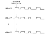
- FIG. 7 is a timing chart for explaining the problem of the conventional scramble process.
- the horizontal axis represents time
- the vertical axis represents each bus.
- the present invention has been made in view of such circumstances, and an object of the present invention is to provide a transmission unit and one or a plurality of reception units that communicate data frames with the transmission unit via a plurality of buses.
- the scramble processing is performed at a different timing for each bus with respect to the communication time of the data frame, thereby further reliably generating EMI noise. It is an object to provide an electric circuit that can be reduced and a display device including the electric circuit.
- An electric circuit includes a transmission unit and one or a plurality of reception units that perform data frame communication with the transmission unit via a plurality of buses, and performs scramble processing when the data frame is communicated.
- the electrical circuit is characterized in that the scramble processing is performed at different timing for each bus with respect to the communication time of the data frame.
- the scramble processing is performed at a timing different for each bus with respect to the communication time of the data frame.
- the electrical circuit according to the present invention is characterized in that the transmission unit includes a delay unit that performs a process of generating an nUI output delay between any two buses.
- n is an integer, except for 0 between any two or more buses, UI: one cycle of the data rate.
- the delay unit of the transmission unit causes an output delay of nUI between any two buses, so that the bus for the communication time of the data frame can be obtained during the communication of the data frame.
- the scramble process is performed at different timings.
- the electric circuit according to the present invention is characterized in that the receiving unit includes a canceling unit that cancels processing by the delay unit with respect to data received from the transmitting unit.
- the canceling unit cancels the processing by the delay unit for the received data.
- the electric circuit according to the present invention is characterized in that the transmission unit includes a scramble unit that performs the scramble process so that an nUI timing difference is generated between data frames of any two buses.
- n is an integer, except for 0 between any two or more buses, UI: one cycle of the data rate.
- the scramble unit of the transmission unit performs the scramble process so that an nUI timing difference between data frames of any two buses, so that the data frame can be transmitted during communication of the data frame.
- the scramble process is performed at different timing for each bus with respect to the frame communication time.
- the electric circuit according to the present invention is characterized in that the reception unit includes a release unit that releases the scramble process by the scramble unit for the data received from the transmission unit.
- the canceling unit cancels the scramble process by the scramble unit for the received data.
- a display device includes the electric circuit according to any one of the foregoing inventions and a liquid crystal display panel connected to the electric circuit, and the liquid crystal is based on data received through the electric circuit.
- the display panel displays an image.
- data in a state in which EMI noise is reduced is transmitted to the liquid crystal display panel through the electrical circuit by the processing by the delay unit or the scramble processing by the scramble unit.
- the display panel displays an image based on the received data.
- the generation of EMI noise can be further reduced without increasing the number of parts (for example, gaskets).
- FIG. 3 is a functional block diagram illustrating a main configuration of the liquid crystal television according to the first embodiment.
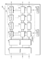
- FIG. 3 is a functional block diagram showing a main configuration of Tcon in the liquid crystal television of the first embodiment.
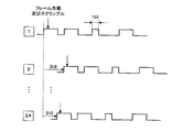
- 4 is a timing chart for explaining processing in which the serializer shifts the timing of the head portion of the data frame in the liquid crystal television according to the first embodiment.
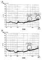
- FIG. 6 is an EMI measurement result when the serializer does not perform processing for shifting the timing of the head portion of the data frame in the liquid crystal television according to Embodiment 1.
- FIG. FIG. 6 is an EMI measurement result when the serializer performs a process of shifting the timing of the head portion of the data frame in the liquid crystal television according to Embodiment 1.
- FIG. 6 is a timing chart for explaining a process in which each scrambler has a different timing of the scramble process in the liquid crystal television according to the second embodiment. It is a timing chart explaining the problem of the conventional scramble process.
- FIG. 1 is a functional block diagram showing a main configuration of the liquid crystal television 100 according to the first embodiment.
- the liquid crystal television 100 receives data from a TVSoC (System a Chip) 10 (transmission unit), a plurality of Tcons (Timing Controller) 20 that receive data from the TVSoC 10, and a Tcon 20 (transmission unit, reception unit).
- a plurality of source drivers 30 (receivers) and a gate driver 40 are provided, and the source driver 30 and the gate driver 40 are connected to a liquid crystal display panel 50 on which an image is displayed based on such data.
- the electric circuit described in the claims includes, for example, TVSoC 10 and Tcon 20, or Tcon 20 and source driver 30.
- the TVSoC 10 is a so-called television receiving circuit, receives a CVBS signal, an HDMI (registered trademark) signal, etc., generates a television image, and outputs an image signal including a television image signal, a horizontal synchronization signal, a vertical synchronization signal, and a clock, for example, Output to Tcon 20 using the V-by-One signal standard.
- the Tcon 20 generates a digital image signal, a control signal for controlling the operation of the drive circuit of the liquid crystal display panel 50, and the like based on a signal (data) from the TVSoC 10.
- the Tcon 20 transmits a digital image signal (hereinafter also simply referred to as an image signal) and a control signal to the source driver 30 and the gate driver 40. That is, the Tcon 20 uses the timing signals such as the vertical synchronization signal (VS), the horizontal synchronization signal (HS), the data enable signal (Data Enable, DE), and the clock signal (CLK) from the TVSoC 10 to control the operation timing of the source driver 30.
- a source timing control signal for controlling and a gate timing control signal for controlling the operation timing of the gate driver 40 are generated.
- the source driver 30 and the gate driver 40 are each composed of one semiconductor integrated circuit (IC), and the Tcon 20 and the source driver 30 are connected by, for example, 24 buses.
- Each pixel (not shown) of the display panel 50 is connected to the source driver 30 and the gate driver 40 via the source line and the gate line.
- FIG. 2 is a functional block diagram showing a main configuration of the Tcon 20 in the liquid crystal television 100 of the first embodiment.
- the Tcon 20 includes a DeSkew 21, a processor 22, and a transmitter 29.
- Tcon 20 Since Tcon 20 receives a signal via the V-by-One signal standard, it receives two signals. The two signals received by the Tcon 20 are converted into 34 / 10-bit parallel signals.
- the DeSkew 21 receives the parallel signal and separates the above-described timing signals excluding the image signals (R, G, B). That is, 30 image signals and 4 timing signals are generated and transmitted to the processor 22.
- the transmitter 29 includes a plurality of command-encoders 23, the same number of scramblers 24, the same number of encoders 25, and the same number of serializers 26.
- the timing signal from the processor 22 and the 24-line / 8-bit image signal are first input to the command-encoder 23.
- the command-encoder 23 receives a predetermined instruction signal (for example, an image signal) from the register A27 together with an image signal for each RGB, a synchronization signal (HS, VS), a data enable signal (DE), and a clock signal (CLK). Such setting values).
- the command-encoder 23 generates a control code based on the data enable signal.
- the command-encoder 23 processes the image signal and the synchronization signal (HS, VS) based on the clock signal (CLK) to generate 24 8-bit parallel packet signals.
- the command-encoder 23 outputs the 8-bit packet signal, the control code, and the clock signal to the scrambler 24.
- the scrambler 24 (scramble unit) has a random number generator (not shown), and scrambles the 8-bit packet signal using the random number from the random number generator.
- the scrambled signal is referred to as a scramble signal.
- the scrambler 24 outputs a scramble signal and the control code to the encoder 25.
- Encoder 25 encodes the scramble signal based on the clock signal (CLK) to generate an encode signal.
- the encoder 25 is an 8b / 10b encoder, and generates a 10-bit encoded signal from an 8-bit scrambled signal.
- the encoder 25 outputs these encoded signals to the serializer 26.
- the serializer 26 (delay unit) performs parallel-serial conversion on the 10-bit encoded signal based on the instruction signal from the register B28 in order to reduce the number of buses.
- a data frame related to the 10-bit encoded signal is transmitted from the Tcon 20 to the source driver 30 using, for example, CalDriCon (registered trademark) which is a driver interface.
- the data frame communication time differs depending on the bus.
- the scramble process is performed at the timing.
- generation of EMI noise in communication between the Tcon 20 and the source driver 30 via a plurality of buses can be suppressed as much as possible. This will be described in detail below.
- the serializer 26 of the Tcon 20 shifts (delays) the head portion of the data frame at a predetermined timing for each bus.
- FIG. 3 is a timing chart for explaining processing in which the serializer 26 shifts the timing of the head portion of the data frame in the liquid crystal television 100 according to the first embodiment.
- the horizontal axis represents time
- the vertical axis represents each bus.
- the serializer 26 generates an nUI output delay between any two buses with respect to the head portion of the data frame, in other words, the data frame itself.
- n is an integer, but 0 is excluded between any two or more buses.
- UI is one cycle of the data rate, in other words, the minimum transmission unit of the data frame.
- the first bus (hereinafter referred to as 1 bus) is not delayed, and is delayed by 3 UI with respect to the 2 bus, and the head portion of the data frame is shifted by that amount. Has been. Also, since any data frame is scrambled at the head, the timing of the scramble process between the 1 bus and the 2 bus with respect to the communication time (including the delay time). Is different.
- the scramble processing is performed at a timing different by 3 UI.
- the 24 buses are delayed by 2 UI, and the timing of the scramble processing is different between the 2 buses and the 24 buses. That is, since the head portion of the data frame is shifted by 1 UI between the 2 bus and the 24 bus, the scramble processing is performed at a timing different by 1 UI.
- liquid crystal television 100 it is possible to prevent the same data from continuing in a plurality of buses, and to reduce the generation of EMI noise as much as possible.
- FIG. 4 shows the EMI measurement results when the serializer 26 does not perform the process of shifting the timing of the head portion of the data frame in the liquid crystal television 100 according to the first embodiment
- FIG. 5 shows the liquid crystal according to the first embodiment. This is an EMI measurement result when a serializer performs processing for shifting the timing of the head portion of a data frame in a television.
- FIG. 5 shows a case where an nUI output delay is caused in only a part of all the buses.
- the horizontal axis represents frequency
- the vertical axis represents level (intensity).
- 4 and FIG. 5A shows the case where the constant antenna is Horizontal
- FIG. 4B and FIG. 5B show the case where the measurement antenna is Vertical.
- Emodiment 2 The present invention is not limited to the liquid crystal television 100 described in the first embodiment.
- each scrambler 24 is configured to perform scramble processing at a different timing for each bus. Accordingly, when data frames are communicated between the Tcon 20 and the source driver 30, the scramble processing can be performed at different timings for each bus with respect to the communication time of the data frames. This will be described in detail below.
- each scrambler 24 corresponding to each bus performs the scramble process on the data frame at different timings. .
- FIG. 6 is a timing chart for explaining a process in which each scrambler 24 has a different timing of the scramble process in the liquid crystal television 100 according to the second embodiment.
- the horizontal axis represents time
- the vertical axis represents each bus.
- each scrambler 24 scrambles the corresponding data frame so that there is an nUI timing difference between the data frames of any two buses.
- n is an integer, but 0 is excluded between any two or more buses.
- UI is one cycle of the data rate, in other words, a minimum transmission unit of a data frame.
- the head part (white arrow) of each data frame is located at the same time.
- the timing (arrow) of the scrambling process for the data frame differs for each bus.
- scramble processing is performed at the beginning of the data frame for 1 bus, and scramble processing is performed after 3 UI for 2 buses. That is, the timing of the scramble process differs between the 1 bus and the 2 bus by 3 UI.
- the scramble processing is performed 1 UI ahead for 2 buses after 2 UI for 1 bus. That is, the timing of the scramble processing is different by 1 UI between the 2 bus and the 24 bus.
- the same data can be prevented from continuing in a plurality of buses as in the first embodiment, and the effect of reducing the generation of EMI noise as much as possible can be achieved. .
- nUI timing difference is present between data frames of any two buses.
- n is an integer, but 0 is excluded between any two or more buses. That is, such a scramble process does not necessarily have to be performed so that the timing difference of the nUI is between the data frames of any two buses, and the scramble process may be performed only in a part. In other words, the scramble process may be performed so that the timing difference is at least nUI between the pair of buses.
- the present invention can also be applied to communication between TVSoC 10 and Tcon 20. Since the TVSoC 10 and the Tcon 20 are connected by a plurality of buses similarly to the Tcon 20 and the source driver 30, EMI noise may occur.
- the TVSoC 10 on the transmission side performs the above-described scramble timing shift processing by the scrambler 24 or the output delay processing by the serializer 26, thereby reducing the generation of EMI noise in the TVSoC 10 and Tcon 20 communication as much as possible. It can be reduced.
- the DeSkew 21 in the Tcon 20 may be configured to perform a process for removing the deformation of the signal (data) from the TVSoC 10. That is, the DeSkew 21 is configured to remove the change due to such processing from the signal from the TVSoC 10 that has been subjected to the shift processing of the timing of the scramble processing or the output delay processing.
- DeSkew21 serves as a release unit described in the claims.
- TVSoC transmitter
- Tcon transmitter, receiver
- DeSkew release part
- Serializer delay unit
- Scrambler Scrambler
- Source driver receiver
- Gate driver 100 LCD television
Landscapes
- Engineering & Computer Science (AREA)
- Physics & Mathematics (AREA)
- Computer Hardware Design (AREA)
- Theoretical Computer Science (AREA)
- General Physics & Mathematics (AREA)
- Signal Processing (AREA)
- Power Engineering (AREA)
- Computer Networks & Wireless Communication (AREA)
- Spectroscopy & Molecular Physics (AREA)
- Chemical & Material Sciences (AREA)
- Crystallography & Structural Chemistry (AREA)
- Control Of Indicators Other Than Cathode Ray Tubes (AREA)
- Liquid Crystal Display Device Control (AREA)
- Multimedia (AREA)
- Synchronisation In Digital Transmission Systems (AREA)
Abstract
Description
図1は実施の形態1の液晶テレビジョン100の要部構成を示す機能ブロック図である。
本発明は実施の形態1に記載の液晶テレビジョン100に限るものでない。
20 Tcon(送信部、受信部)
21 DeSkew(解除部)
26 シリアライザ(遅延部)
24 スクランブラ(スクランブル部)
30 ソースドライバ(受信部)
40 ゲートドライバ
100 液晶テレビジョン
Claims (6)
- 送信部、及び、複数のバスを介して該送信部とデータフレームの通信を行う一又は複数の受信部を備え、前記データフレームの通信の際、スクランブル処理を行う電気回路において、
前記データフレームの通信時間に対してバス毎に異なるタイミングで前記スクランブル処理を行うことを特徴とする電気回路。 - 前記送信部は、任意の2つのバス間にnUIの出力遅延を生じさせる処理を行う遅延部を備えることを特徴とする請求項1に記載の電気回路。
但し、n:整数、ただし任意の2つ以上のバス間は0を除く、UI:データレートの1周期。 - 前記受信部は、前記送信部から受信したデータに対して、前記遅延部による処理を解除する解除部を備えることを特徴とする請求項2に記載の電気回路。
- 前記送信部は、任意の2つのバスのデータフレーム間でnUIのタイミング差になるように前記スクランブル処理を行うスクランブル部を備えることを特徴とする請求項1に記載の電気回路。
但し、n:整数、ただし任意の2つ以上のバス間は0を除く、UI:データレートの1周期。 - 前記受信部は、前記送信部から受信したデータに対して、前記スクランブル部によるスクランブル処理を解除する解除部を備えることを特徴とする請求項4に記載の電気回路。
- 請求項1~5の何れかに記載の電気回路と、
該電気回路に接続された液晶表示パネルとを備え、
前記電気回路を介して受信したデータに基づいて、前記液晶表示パネルが画像表示を行うことを特徴とする表示装置。
Priority Applications (4)
| Application Number | Priority Date | Filing Date | Title |
|---|---|---|---|
| PCT/JP2015/064485 WO2016185585A1 (ja) | 2015-05-20 | 2015-05-20 | 電気回路及び表示装置 |
| US15/574,751 US10515578B2 (en) | 2015-05-20 | 2015-05-20 | Electrical circuit and display apparatus |
| CN201580080185.4A CN107615700B (zh) | 2015-05-20 | 2015-05-20 | 电路和显示装置 |
| JP2017518687A JP6473808B2 (ja) | 2015-05-20 | 2015-05-20 | 電気回路及び表示装置 |
Applications Claiming Priority (1)
| Application Number | Priority Date | Filing Date | Title |
|---|---|---|---|
| PCT/JP2015/064485 WO2016185585A1 (ja) | 2015-05-20 | 2015-05-20 | 電気回路及び表示装置 |
Publications (1)
| Publication Number | Publication Date |
|---|---|
| WO2016185585A1 true WO2016185585A1 (ja) | 2016-11-24 |
Family
ID=57319682
Family Applications (1)
| Application Number | Title | Priority Date | Filing Date |
|---|---|---|---|
| PCT/JP2015/064485 Ceased WO2016185585A1 (ja) | 2015-05-20 | 2015-05-20 | 電気回路及び表示装置 |
Country Status (4)
| Country | Link |
|---|---|
| US (1) | US10515578B2 (ja) |
| JP (1) | JP6473808B2 (ja) |
| CN (1) | CN107615700B (ja) |
| WO (1) | WO2016185585A1 (ja) |
Cited By (1)
| Publication number | Priority date | Publication date | Assignee | Title |
|---|---|---|---|---|
| EP3637398A4 (en) * | 2017-06-09 | 2020-12-02 | Boe Technology Group Co. Ltd. | SIGNAL TRANSMISSION PROCESS AND ASSOCIATED SYNCHRONIZATION CONTROLLER, SOURCE CONTROL DEVICE AND DISPLAY DEVICE |
Families Citing this family (4)
| Publication number | Priority date | Publication date | Assignee | Title |
|---|---|---|---|---|
| JP6473808B2 (ja) * | 2015-05-20 | 2019-02-20 | 堺ディスプレイプロダクト株式会社 | 電気回路及び表示装置 |
| CN109036328B (zh) * | 2017-06-09 | 2021-09-03 | 京东方科技集团股份有限公司 | 寄存器值传输方法及组件、显示装置 |
| US11250753B2 (en) * | 2020-04-16 | 2022-02-15 | Synaptics Incorporated | EMI mitigation by shifted source line pre-charge |
| JP2024167948A (ja) * | 2023-05-23 | 2024-12-05 | ローム株式会社 | データ通信システム、送信回路及び表示装置 |
Citations (3)
| Publication number | Priority date | Publication date | Assignee | Title |
|---|---|---|---|---|
| JPH01213042A (ja) * | 1988-02-22 | 1989-08-25 | Fujitsu Ltd | 多重化方式 |
| WO2010109668A1 (ja) * | 2009-03-27 | 2010-09-30 | 富士通株式会社 | 位相調整方法、データ転送装置およびデータ転送システム |
| JP2014529269A (ja) * | 2011-09-30 | 2014-10-30 | インテル コーポレイション | 高速通信リンクのトレーニング中に電源ノイズを低減する方法及びシステム |
Family Cites Families (24)
| Publication number | Priority date | Publication date | Assignee | Title |
|---|---|---|---|---|
| US6636607B1 (en) * | 1998-10-08 | 2003-10-21 | Ati International Srl | Method and apparatus for controlling display of content signals |
| JP2004138933A (ja) * | 2002-10-21 | 2004-05-13 | Hitachi Ltd | デジタル映像スクランブル装置、デスクランブル装置および該装置を実現するプログラム |
| US7095407B1 (en) * | 2003-04-25 | 2006-08-22 | National Semiconductor Corporation | Method and apparatus for reducing noise in a graphics display system |
| JP3821111B2 (ja) * | 2003-05-12 | 2006-09-13 | セイコーエプソン株式会社 | データドライバ及び電気光学装置 |
| CN100505731C (zh) * | 2003-07-11 | 2009-06-24 | 威盛电子股份有限公司 | 网络接口电路及其方法 |
| US20060061517A1 (en) * | 2004-09-23 | 2006-03-23 | Jolly Paul A | Delivering pixels received at a lower data transfer rate over an interface that operates at a higher data transfer rate |
| JP4974623B2 (ja) * | 2006-09-14 | 2012-07-11 | ルネサスエレクトロニクス株式会社 | 平面表示装置の駆動回路およびデータドライバ |
| JP5041590B2 (ja) * | 2007-07-09 | 2012-10-03 | ルネサスエレクトロニクス株式会社 | 平面表示装置、データ処理方法 |
| JP5392533B2 (ja) * | 2008-10-10 | 2014-01-22 | ソニー株式会社 | 固体撮像素子、光学装置、信号処理装置及び信号処理システム |
| KR101318272B1 (ko) * | 2009-12-30 | 2013-10-16 | 엘지디스플레이 주식회사 | 데이터 전송 장치 및 이를 이용한 평판 표시 장치 |
| US8362997B2 (en) * | 2010-02-12 | 2013-01-29 | Au Optronics Corporation | Display with CLK phase or data phase auto-adjusting mechanism and method of driving same |
| JP5896503B2 (ja) | 2010-08-03 | 2016-03-30 | ザインエレクトロニクス株式会社 | 送信装置、受信装置および送受信システム |
| JP2012042575A (ja) * | 2010-08-16 | 2012-03-01 | Renesas Electronics Corp | 表示装置、信号線ドライバ、及び、データ転送方法 |
| US9838226B2 (en) * | 2012-01-27 | 2017-12-05 | Apple Inc. | Methods and apparatus for the intelligent scrambling of control symbols |
| KR101333519B1 (ko) * | 2012-04-30 | 2013-11-27 | 엘지디스플레이 주식회사 | 액정표시장치 및 그 구동 방법 |
| CN103903573B (zh) * | 2012-12-26 | 2016-05-11 | 联咏科技股份有限公司 | 时序扰乱方法及其时序控制装置 |
| TWI506610B (zh) * | 2013-02-20 | 2015-11-01 | Novatek Microelectronics Corp | 顯示驅動裝置及顯示面板的驅動方法 |
| KR20150019884A (ko) * | 2013-08-16 | 2015-02-25 | 삼성전자주식회사 | 디스플레이 구동 회로 및 디스플레이 장치 |
| KR102151949B1 (ko) * | 2013-12-30 | 2020-09-04 | 엘지디스플레이 주식회사 | 표시장치와 그 구동 방법 |
| US9953598B2 (en) * | 2014-05-29 | 2018-04-24 | Samsung Electronics Co., Ltd. | Method of controlling display driver IC with improved noise characteristics |
| JP6425115B2 (ja) * | 2014-07-03 | 2018-11-21 | Tianma Japan株式会社 | タイミングコントローラ及び表示装置 |
| KR102253824B1 (ko) * | 2015-01-13 | 2021-05-21 | 삼성디스플레이 주식회사 | 타이밍 컨트롤러 및 그것을 포함하는 표시 장치 |
| JP6473808B2 (ja) * | 2015-05-20 | 2019-02-20 | 堺ディスプレイプロダクト株式会社 | 電気回路及び表示装置 |
| KR102645150B1 (ko) * | 2016-12-30 | 2024-03-07 | 엘지디스플레이 주식회사 | 디스플레이 인터페이스 장치 및 그의 데이터 전송 방법 |
-
2015
- 2015-05-20 JP JP2017518687A patent/JP6473808B2/ja active Active
- 2015-05-20 US US15/574,751 patent/US10515578B2/en active Active
- 2015-05-20 CN CN201580080185.4A patent/CN107615700B/zh active Active
- 2015-05-20 WO PCT/JP2015/064485 patent/WO2016185585A1/ja not_active Ceased
Patent Citations (3)
| Publication number | Priority date | Publication date | Assignee | Title |
|---|---|---|---|---|
| JPH01213042A (ja) * | 1988-02-22 | 1989-08-25 | Fujitsu Ltd | 多重化方式 |
| WO2010109668A1 (ja) * | 2009-03-27 | 2010-09-30 | 富士通株式会社 | 位相調整方法、データ転送装置およびデータ転送システム |
| JP2014529269A (ja) * | 2011-09-30 | 2014-10-30 | インテル コーポレイション | 高速通信リンクのトレーニング中に電源ノイズを低減する方法及びシステム |
Cited By (2)
| Publication number | Priority date | Publication date | Assignee | Title |
|---|---|---|---|---|
| EP3637398A4 (en) * | 2017-06-09 | 2020-12-02 | Boe Technology Group Co. Ltd. | SIGNAL TRANSMISSION PROCESS AND ASSOCIATED SYNCHRONIZATION CONTROLLER, SOURCE CONTROL DEVICE AND DISPLAY DEVICE |
| US10923070B2 (en) | 2017-06-09 | 2021-02-16 | Beijing Boe Display Technology Co., Ltd. | Signal transmission method, related timing controller, source driver and display device |
Also Published As
| Publication number | Publication date |
|---|---|
| JPWO2016185585A1 (ja) | 2018-03-08 |
| US20180151107A1 (en) | 2018-05-31 |
| JP6473808B2 (ja) | 2019-02-20 |
| US10515578B2 (en) | 2019-12-24 |
| CN107615700B (zh) | 2020-08-11 |
| CN107615700A (zh) | 2018-01-19 |
Similar Documents
| Publication | Publication Date | Title |
|---|---|---|
| JP6473808B2 (ja) | 電気回路及び表示装置 | |
| US8780932B2 (en) | Video signal transmission device, video signal reception device, and video signal transmission system | |
| US8362997B2 (en) | Display with CLK phase or data phase auto-adjusting mechanism and method of driving same | |
| JP4192802B2 (ja) | デジタル映像通信装置 | |
| US9036081B2 (en) | Video signal transmission device, video signal reception device, and video signal transmission system | |
| CN103903577B (zh) | 显示装置及其驱动方法、时序控制电路的数据处理及输出方法 | |
| US9270443B2 (en) | Serial data transmission circuit and reception circuit, transmission system using the same, electronic device, and serial data transmission method | |
| JP2012029214A (ja) | インタフェース回路およびそれを用いた電子機器 | |
| US20130216235A1 (en) | Transmission system and electronic equipment | |
| TWI637602B (zh) | 透過利用最小化傳輸差分訊號碼之一通信介面以用於傳輸編碼保護頻帶資料 | |
| KR20190075591A (ko) | 디스플레이 패널구동장치 및 디스플레이 장치에서의 영상데이터송수신방법 | |
| US8922535B2 (en) | Timing controller, source driver, display driving circuit, and display driving method | |
| US9898993B2 (en) | Method for controlling message signal within timing controller integrated circuit, timing controller integrated circuit and display panel | |
| JP2012181500A (ja) | 映像信号処理回路、該処理回路に用いられる映像信号処理方法、及び画像表示装置 | |
| CN106952600B (zh) | 时序控制器及其信号输出方法 | |
| US10096297B2 (en) | Display device, display panel driver, and image data signal transmission method | |
| US20250227199A1 (en) | Data transmitter and display device including the same | |
| CN103810975B (zh) | 时序控制器、源极驱动器、显示驱动电路及显示驱动方法 | |
| US9130625B2 (en) | Interference avoidance method of pulse signal and terminal applicable thereto | |
| KR20110076262A (ko) | 휴대용 단말기에서 emi 노이즈를 저감하기 위한 장치 및 방법 | |
| US10791349B2 (en) | Frame generation apparatus, frame generation method, image synthesis apparatus, image synthesis method, signal generation apparatus, signal generation method, and image transmission system | |
| JP2012023471A (ja) | インタフェース回路およびそれを用いた電子機器 | |
| JP2010028229A (ja) | 著作権保護回路及び映像表示装置 | |
| CN114430912A (zh) | 数字视像信号生成电路、数字视像信号生成系统、数字视像信号生成方法及非易失性存储介质 | |
| JP2015145911A (ja) | 表示装置、表示装置の制御方法 |
Legal Events
| Date | Code | Title | Description |
|---|---|---|---|
| 121 | Ep: the epo has been informed by wipo that ep was designated in this application |
Ref document number: 15892584 Country of ref document: EP Kind code of ref document: A1 |
|
| ENP | Entry into the national phase |
Ref document number: 2017518687 Country of ref document: JP Kind code of ref document: A |
|
| WWE | Wipo information: entry into national phase |
Ref document number: 15574751 Country of ref document: US |
|
| NENP | Non-entry into the national phase |
Ref country code: DE |
|
| 122 | Ep: pct application non-entry in european phase |
Ref document number: 15892584 Country of ref document: EP Kind code of ref document: A1 |