WO2016176879A1 - Amoled背板的制作方法及其结构 - Google Patents
Amoled背板的制作方法及其结构 Download PDFInfo
- Publication number
- WO2016176879A1 WO2016176879A1 PCT/CN2015/079535 CN2015079535W WO2016176879A1 WO 2016176879 A1 WO2016176879 A1 WO 2016176879A1 CN 2015079535 W CN2015079535 W CN 2015079535W WO 2016176879 A1 WO2016176879 A1 WO 2016176879A1
- Authority
- WO
- WIPO (PCT)
- Prior art keywords
- layer
- polysilicon
- drain
- gate
- source
- Prior art date
- Legal status (The legal status is an assumption and is not a legal conclusion. Google has not performed a legal analysis and makes no representation as to the accuracy of the status listed.)
- Ceased
Links
Images




Classifications
-
- H—ELECTRICITY
- H10—SEMICONDUCTOR DEVICES; ELECTRIC SOLID-STATE DEVICES NOT OTHERWISE PROVIDED FOR
- H10D—INORGANIC ELECTRIC SEMICONDUCTOR DEVICES
- H10D86/00—Integrated devices formed in or on insulating or conducting substrates, e.g. formed in silicon-on-insulator [SOI] substrates or on stainless steel or glass substrates
- H10D86/40—Integrated devices formed in or on insulating or conducting substrates, e.g. formed in silicon-on-insulator [SOI] substrates or on stainless steel or glass substrates characterised by multiple TFTs
- H10D86/481—Integrated devices formed in or on insulating or conducting substrates, e.g. formed in silicon-on-insulator [SOI] substrates or on stainless steel or glass substrates characterised by multiple TFTs integrated with passive devices, e.g. auxiliary capacitors
-
- H—ELECTRICITY
- H10—SEMICONDUCTOR DEVICES; ELECTRIC SOLID-STATE DEVICES NOT OTHERWISE PROVIDED FOR
- H10D—INORGANIC ELECTRIC SEMICONDUCTOR DEVICES
- H10D86/00—Integrated devices formed in or on insulating or conducting substrates, e.g. formed in silicon-on-insulator [SOI] substrates or on stainless steel or glass substrates
- H10D86/01—Manufacture or treatment
- H10D86/021—Manufacture or treatment of multiple TFTs
- H10D86/0221—Manufacture or treatment of multiple TFTs comprising manufacture, treatment or patterning of TFT semiconductor bodies
- H10D86/0223—Manufacture or treatment of multiple TFTs comprising manufacture, treatment or patterning of TFT semiconductor bodies comprising crystallisation of amorphous, microcrystalline or polycrystalline semiconductor materials
-
- H—ELECTRICITY
- H10—SEMICONDUCTOR DEVICES; ELECTRIC SOLID-STATE DEVICES NOT OTHERWISE PROVIDED FOR
- H10D—INORGANIC ELECTRIC SEMICONDUCTOR DEVICES
- H10D86/00—Integrated devices formed in or on insulating or conducting substrates, e.g. formed in silicon-on-insulator [SOI] substrates or on stainless steel or glass substrates
- H10D86/01—Manufacture or treatment
- H10D86/021—Manufacture or treatment of multiple TFTs
- H10D86/0231—Manufacture or treatment of multiple TFTs using masks, e.g. half-tone masks
-
- H—ELECTRICITY
- H10—SEMICONDUCTOR DEVICES; ELECTRIC SOLID-STATE DEVICES NOT OTHERWISE PROVIDED FOR
- H10D—INORGANIC ELECTRIC SEMICONDUCTOR DEVICES
- H10D86/00—Integrated devices formed in or on insulating or conducting substrates, e.g. formed in silicon-on-insulator [SOI] substrates or on stainless steel or glass substrates
- H10D86/40—Integrated devices formed in or on insulating or conducting substrates, e.g. formed in silicon-on-insulator [SOI] substrates or on stainless steel or glass substrates characterised by multiple TFTs
- H10D86/60—Integrated devices formed in or on insulating or conducting substrates, e.g. formed in silicon-on-insulator [SOI] substrates or on stainless steel or glass substrates characterised by multiple TFTs wherein the TFTs are in active matrices
-
- H—ELECTRICITY
- H10—SEMICONDUCTOR DEVICES; ELECTRIC SOLID-STATE DEVICES NOT OTHERWISE PROVIDED FOR
- H10K—ORGANIC ELECTRIC SOLID-STATE DEVICES
- H10K50/00—Organic light-emitting devices
- H10K50/80—Constructional details
- H10K50/805—Electrodes
-
- H—ELECTRICITY
- H10—SEMICONDUCTOR DEVICES; ELECTRIC SOLID-STATE DEVICES NOT OTHERWISE PROVIDED FOR
- H10K—ORGANIC ELECTRIC SOLID-STATE DEVICES
- H10K50/00—Organic light-emitting devices
- H10K50/80—Constructional details
- H10K50/805—Electrodes
- H10K50/81—Anodes
- H10K50/818—Reflective anodes, e.g. ITO combined with thick metallic layers
-
- H—ELECTRICITY
- H10—SEMICONDUCTOR DEVICES; ELECTRIC SOLID-STATE DEVICES NOT OTHERWISE PROVIDED FOR
- H10K—ORGANIC ELECTRIC SOLID-STATE DEVICES
- H10K59/00—Integrated devices, or assemblies of multiple devices, comprising at least one organic light-emitting element covered by group H10K50/00
-
- H—ELECTRICITY
- H10—SEMICONDUCTOR DEVICES; ELECTRIC SOLID-STATE DEVICES NOT OTHERWISE PROVIDED FOR
- H10K—ORGANIC ELECTRIC SOLID-STATE DEVICES
- H10K59/00—Integrated devices, or assemblies of multiple devices, comprising at least one organic light-emitting element covered by group H10K50/00
- H10K59/10—OLED displays
- H10K59/12—Active-matrix OLED [AMOLED] displays
- H10K59/1201—Manufacture or treatment
-
- H—ELECTRICITY
- H10—SEMICONDUCTOR DEVICES; ELECTRIC SOLID-STATE DEVICES NOT OTHERWISE PROVIDED FOR
- H10K—ORGANIC ELECTRIC SOLID-STATE DEVICES
- H10K59/00—Integrated devices, or assemblies of multiple devices, comprising at least one organic light-emitting element covered by group H10K50/00
- H10K59/10—OLED displays
- H10K59/12—Active-matrix OLED [AMOLED] displays
- H10K59/121—Active-matrix OLED [AMOLED] displays characterised by the geometry or disposition of pixel elements
- H10K59/1213—Active-matrix OLED [AMOLED] displays characterised by the geometry or disposition of pixel elements the pixel elements being TFTs
-
- H—ELECTRICITY
- H10—SEMICONDUCTOR DEVICES; ELECTRIC SOLID-STATE DEVICES NOT OTHERWISE PROVIDED FOR
- H10K—ORGANIC ELECTRIC SOLID-STATE DEVICES
- H10K59/00—Integrated devices, or assemblies of multiple devices, comprising at least one organic light-emitting element covered by group H10K50/00
- H10K59/10—OLED displays
- H10K59/12—Active-matrix OLED [AMOLED] displays
- H10K59/121—Active-matrix OLED [AMOLED] displays characterised by the geometry or disposition of pixel elements
- H10K59/1216—Active-matrix OLED [AMOLED] displays characterised by the geometry or disposition of pixel elements the pixel elements being capacitors
-
- H—ELECTRICITY
- H10—SEMICONDUCTOR DEVICES; ELECTRIC SOLID-STATE DEVICES NOT OTHERWISE PROVIDED FOR
- H10K—ORGANIC ELECTRIC SOLID-STATE DEVICES
- H10K71/00—Manufacture or treatment specially adapted for the organic devices covered by this subclass
-
- H—ELECTRICITY
- H10—SEMICONDUCTOR DEVICES; ELECTRIC SOLID-STATE DEVICES NOT OTHERWISE PROVIDED FOR
- H10K—ORGANIC ELECTRIC SOLID-STATE DEVICES
- H10K59/00—Integrated devices, or assemblies of multiple devices, comprising at least one organic light-emitting element covered by group H10K50/00
- H10K59/80—Constructional details
- H10K59/805—Electrodes
- H10K59/8051—Anodes
- H10K59/80517—Multilayers, e.g. transparent multilayers
Definitions
- the present invention relates to the field of display technologies, and in particular, to a method and a structure for fabricating an AMOLED backplane.
- OLED organic light emitting diodes
- OLEDs can be classified into passive OLEDs (PMOLEDs) and active OLEDs (AMOLEDs) according to the type of driving.
- the AMOLED is usually composed of a low temperature poly-Silicon (LTPS) driven backplane and an electroluminescent layer to form a self-illuminating component.
- LTPS low temperature poly-Silicon
- electroluminescent layer to form a self-illuminating component.
- Low-temperature polysilicon has high electron mobility.
- low-temperature polysilicon material has the advantages of high resolution, fast reaction speed, high brightness, high aperture ratio, and low energy consumption.
- FIG. 1 is a schematic cross-sectional view of a conventional AMOLED backplane.
- the manufacturing method of the AMOLED backplane mainly includes the following steps:
- Step 1 providing a substrate 100, depositing a buffer layer 200 on the substrate 100;
- Step 2 depositing an amorphous silicon layer on the buffer layer 200, and crystallizing the amorphous silicon layer into a polysilicon layer by excimer laser annealing treatment, and then patterning the polysilicon layer through a mask process Processing, forming mutually spaced first polysilicon segments 310, second polysilicon segments 320, and third polysilicon segments 330;
- Step 3 depositing a gate insulating layer 400 on the first polysilicon segment 310, the second polysilicon segment 320, the third polysilicon segment 330, and the buffer layer 200;
- Step 4 depositing a first photoresist layer on the gate insulating layer 400 and patterning the first photoresist layer through a mask process;
- the first photoresist layer shields the first polysilicon segment 310 and the middle portion of the second polysilicon segment 320, and does not shield the third polysilicon segment 330;
- First polysilicon segment 310 Forming a P-type heavily doped region P+ on both sides of the second polysilicon segment 320 and the entire third polysilicon segment 330;
- Step 5 removing the first photoresist layer, depositing a first metal layer on the gate insulating layer 400 and patterning the first metal layer through a mask process to form a first gate 610 and a second gate 620, and a metal electrode 630;
- Step 6 Deposit an interlayer insulating layer 700 on the first gate 610, the second gate 620, the metal electrode 630, and the gate insulating layer 400, and process the interlayer insulating layer 700 through a mask process. And a first via 710 is formed on the gate insulating layer 400 corresponding to the first polysilicon segment 310 and the P-type heavily doped region P+ at both ends of the second polysilicon segment 320;
- Step 7 depositing a second metal layer on the interlayer insulating layer 700 and patterning the second metal layer through a mask process to form a first source/drain 810, and a second source/drain 820;
- the first source/drain 810 and the second source/drain 820 pass through the first via 710 and the first polysilicon segment 310 and the P-type at both ends of the second polysilicon segment 320, respectively.
- the heavily doped region P+ is in contact;
- Step 8 forming a flat layer 830 on the first source/drain 810, the second source/drain 820, and the interlayer insulating layer 700, and corresponding to the flat layer 830 through a mask process Forming a second via 840 above the second source/drain 820;
- Step 9 depositing a conductive film on the flat layer 830 and patterning the conductive film through a mask process to form an anode 850;
- the anode 850 is in contact with the second source/drain 820 via the second via 840;
- Step 10 depositing a second photoresist layer on the anode 850, and the flat layer 830, and patterning the second photoresist layer through a mask process to form a pixel defining layer 900;
- Step 11 Deposit a third photoresist layer on the pixel defining layer 900 and the anode 850, and pattern the third photoresist layer through a mask process to form a photoresist spacer 910.
- the object of the present invention is to provide a method for fabricating an AMOLED backplane, which is simple in process, can reduce the number of masks in the process, improve production efficiency, save cost, and avoid uneven brightness of display caused by excimer laser annealing treatment. .
- Another object of the present invention is to provide an AMOLED backplane structure which is simple in structure, easy to manufacture, and low in cost.
- the present invention provides a method for fabricating an AMOLED backplane, comprising the following steps:
- Step 1 Providing a substrate, the substrate comprising a switching TFT region, a storage capacitor region, and a driving TFT region, depositing a first metal layer on the substrate and patterning the first metal layer through a mask process, respectively forming a location a first gate of the switching TFT region, a second gate located in the driving TFT region, and a first metal electrode located in the storage capacitor region;
- Step 2 depositing a gate insulating layer on the first gate, the second gate, and the first metal electrode;
- Step 3 sequentially depositing an amorphous silicon layer and a P-type heavily doped amorphous silicon layer on the gate insulating layer, and performing the amorphous silicon layer and the P-type heavily doped amorphous by a solid phase crystallization process
- the silicon layer crystals are respectively converted into a polysilicon layer and a P-type heavily doped polysilicon layer, and then the polysilicon layer and the P-type heavily doped polysilicon layer are simultaneously patterned by a mask process to form respectively on the first gate a first polysilicon segment above the second gate and the second polysilicon segment;
- Step 4 depositing a second metal layer on the first polysilicon segment, the second polysilicon segment, and the gate insulating layer and patterning the second metal layer through a mask process to form respectively a first gate, a second gate, and first source/drain, second source/drain, and second metal electrode over the first metal electrode;
- the first source/drain and the second source/drain are respectively in contact with the P-type heavily doped polysilicon layer in the first polysilicon segment and the second polysilicon segment;
- Step 5 depositing a passivation layer on the first source/drain, the second source/drain, the second metal electrode, and the gate insulating layer;
- Step 6 Apply a flat layer on the passivation layer, and form a via hole on the flat layer and the passivation layer corresponding to the second source/drain through a mask process;
- Step 7 Depositing a conductive film on the flat layer and patterning the conductive film through a mask process to form a pixel electrode layer, and the pixel electrode layer and the second source/drain phase via the via hole contact;
- Step 8 Applying a first organic photoresist layer on the pixel electrode layer and the planar layer and patterning the first organic photoresist layer through a mask process to form a pixel defining layer;
- Step 9 Applying a second organic photoresist layer on the pixel defining layer and the pixel electrode layer, and patterning the second organic photoresist layer through a mask process to form a photoresist spacer;
- the first polysilicon segment, the first gate and the first source/drain constitute a switching TFT; the second polysilicon segment, the second gate and the second source/drain constitute a driving TFT; The first metal electrode and the second metal electrode constitute a storage capacitor.
- the material of the first gate, the second gate, and the first metal electrode in the step 1 is molybdenum or copper.
- the gate insulating layer in the step 2 is a silicon oxide layer, a silicon nitride layer, or a multilayer composite structure composed of a silicon oxide layer and a silicon nitride layer.
- the passivation layer in the step 5 is a silicon oxide layer, a silicon nitride layer, or a multilayer composite structure composed of a silicon oxide layer and a silicon nitride layer.
- the conductive film that is, the pixel electrode layer is a three-layer structure in which two conductive oxide layers are sandwiched by a metal layer, and the conductive oxide layer is made of indium tin oxide.
- the material of the metal layer is silver or aluminum.
- the present invention also provides an AMOLED backplane structure, including a substrate, a first gate, a second gate, and a first metal electrode disposed on the substrate, and disposed on the first gate and the second gate And a gate insulating layer on the first metal electrode, a first polysilicon segment disposed on the gate insulating layer, and a second polysilicon segment, disposed in the first polysilicon segment, a second polysilicon segment, and a first source/drain, a second source/drain, and a second metal electrode on the gate insulating layer, disposed on the first source/drain and the second source/drain a second metal electrode and a passivation layer on the gate insulating layer, a flat layer provided on the passivation layer, a pixel electrode layer disposed on the flat layer, and the pixel and the pixel a pixel defining layer on the electrode layer, and a photoresist spacer disposed on the pixel defining layer;
- the first polysilicon segment and the second polysilicon segment each include a polysilicon layer and a P-type heavily doped polysilicon layer sequentially disposed on the gate insulating layer; the first source/drain, and the second The source/drain are respectively in contact with the P-type heavily doped polysilicon layer in the first polysilicon segment and the second polysilicon segment; the planar layer and the passivation layer corresponding to the second source a via hole is disposed above the drain, and the pixel electrode layer is in contact with the second source/drain via the via hole;
- the first polysilicon segment, the first gate and the first source/drain constitute a switching TFT; the second polysilicon segment, the second gate and the second source/drain constitute a driving TFT; The first metal electrode and the second metal electrode constitute a storage capacitor.
- the material of the first gate, the second gate, and the first metal electrode is molybdenum or copper.
- the gate insulating layer is a silicon oxide layer, a silicon nitride layer, or a multilayer composite structure composed of a silicon oxide layer and a silicon nitride layer;
- the passivation layer is a silicon oxide layer, a silicon nitride layer, or A multilayer composite structure composed of a silicon oxide layer and a silicon nitride layer.
- the first polysilicon segment and the second polysilicon segment further include a first channel on the polysilicon layer and located in a middle portion of the first polysilicon segment and a middle portion of the second polysilicon segment, and Second channel.
- the pixel electrode layer is a three-layer structure composed of a metal oxide layer sandwiched by two conductive oxide layers.
- the conductive oxide layer is made of indium tin oxide, and the metal layer is made of silver or aluminum.
- the present invention also provides an AMOLED backplane structure, including a substrate, a first gate, a second gate, and a first metal electrode disposed on the substrate, and disposed on the first gate and the second gate And a gate insulating layer on the first metal electrode, a first polysilicon segment disposed on the gate insulating layer, and a second polysilicon segment, disposed in the first polysilicon segment, a second polysilicon segment, and a first source/drain, a second source/drain, and a second metal electrode on the gate insulating layer, disposed on the first source/drain and the second source/drain a second metal electrode and a passivation layer on the gate insulating layer, a flat layer provided on the passivation layer, a pixel electrode layer disposed on the flat layer, and the pixel and the pixel a pixel defining layer on the electrode layer, and a photoresist spacer disposed on the pixel defining layer;
- the first polysilicon segment and the second polysilicon segment each include a polysilicon layer and a P-type heavily doped polysilicon layer sequentially disposed on the gate insulating layer; the first source/drain, and the second The source/drain are respectively in contact with the P-type heavily doped polysilicon layer in the first polysilicon segment and the second polysilicon segment; the planar layer and the passivation layer corresponding to the second source a via hole is disposed above the drain, and the pixel electrode layer is in contact with the second source/drain via the via hole;
- the first polysilicon segment, the first gate and the first source/drain constitute a switching TFT;
- the second polysilicon segment, the second gate and the second source/drain constitute a driving TFT;
- the first metal electrode and the second metal electrode constitute a storage capacitor;
- the material of the first gate, the second gate, and the first metal electrode is molybdenum or copper
- the gate insulating layer is a silicon oxide layer, a silicon nitride layer, or a multilayer composite structure composed of a silicon oxide layer and a silicon nitride layer;
- the passivation layer is a silicon oxide layer, a silicon nitride layer, Or a multilayer composite structure composed of a silicon oxide layer and a silicon nitride layer;
- the first polysilicon segment and the second polysilicon segment further include a first channel on the polysilicon layer and respectively located in a middle portion of the first polysilicon segment and a middle portion of the second polysilicon segment And a second channel;
- the pixel electrode layer is a three-layer structure composed of a metal oxide layer sandwiched by two conductive oxide layers.
- the conductive oxide layer is made of indium tin oxide, and the metal layer is made of silver or aluminum.
- the invention has the beneficial effects that the method for fabricating the AMOLED back sheet of the invention adopts a solid phase crystallization process to crystallize and convert the amorphous silicon into polycrystalline silicon, thereby avoiding the problem of uneven brightness of the display caused by excimer laser annealing treatment, and adopting the back
- the channel etch type structure effectively reduces the number of reticle used.
- the method for fabricating the AMOLED backplane of the present invention only needs to adopt a 7-mask process, which saves two mask processes compared with the prior art, thereby simplifying the process. Process, improve production efficiency and save costs.
- the AMOLED backplane structure of the invention adopts a solid phase crystallization process to crystallize and convert amorphous silicon into polycrystalline silicon, thereby avoiding display brightness generated by excimer laser annealing treatment
- the problem of unequality and the use of a back channel etch type structure is simple in structure, easy to manufacture, and low in cost.
- FIG. 1 is a schematic cross-sectional structural view of a conventional AMOLED backplane
- FIG. 2 is a flow chart of a method for fabricating an AMOLED backplane according to the present invention
- step 1 is a schematic diagram of step 1 of a method for fabricating an AMOLED backplane according to the present invention
- step 2 is a schematic diagram of step 2 of a method for fabricating an AMOLED backplane according to the present invention
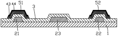
- FIG. 5-7 are schematic diagrams of step 3 of a method for fabricating an AMOLED backplane according to the present invention.
- step 4 is a schematic diagram of step 4 of a method for fabricating an AMOLED backplane according to the present invention.
- step 5 is a schematic diagram of step 5 of a method for fabricating an AMOLED backplane according to the present invention.
- FIG. 10 is a schematic diagram of step 6 of a method for fabricating an AMOLED backplane according to the present invention.
- step 7 is a schematic diagram of step 7 of a method for fabricating an AMOLED backplane according to the present invention.
- step 8 is a schematic diagram of step 8 of a method for fabricating an AMOLED backplane according to the present invention.
- FIG. 13 is a schematic diagram of the step 9 of the method for fabricating the AMOLED backplane of the present invention and a cross-sectional view of the AMOLED backplane structure of the present invention.
- the present invention provides a method for fabricating an AMOLED backplane, including the following steps:
- a substrate 1 is provided.
- the substrate 1 includes a switching TFT region, a storage capacitor region, and a driving TFT region.
- a first metal layer is deposited on the substrate 1 and patterned by a mask process. The first metal layer respectively forms a first gate electrode 21 located in the switching TFT region, a second gate electrode 22 located in the driving TFT region, and a first metal electrode 23 located in the storage capacitor region.
- materials of the first gate 21, the second gate 22, and the first metal electrode 23 It may be molybdenum (Mo) or copper (Cu).
- Step 2 As shown in FIG. 4, a gate insulating layer 3 is deposited on the first gate 21, the second gate 22, and the first metal electrode 23.
- the material of the gate insulating layer 3 may be silicon oxide (SiOx), silicon nitride (SiNx), or a combination of the two.
- Step 3 as shown in FIG. 5-7, an amorphous silicon layer 41 and a P-type heavily doped amorphous silicon layer 42 are sequentially deposited on the gate insulating layer 3, and the non-crystalline layer is formed by a solid phase crystallization process.
- the crystalline silicon layer 41 and the P-type heavily doped amorphous silicon layer 42 are respectively converted into a polysilicon layer 43 and a P-type heavily doped polysilicon layer 44, and then simultaneously doped into the polysilicon layer 43 and the P-type through a mask process.
- the doped polysilicon layer 44 is patterned to form a first polysilicon segment 51 and a second polysilicon segment 52 respectively above the first gate 21 and the second gate 22.
- the solid phase crystallization process is used to crystallize and convert amorphous silicon into polycrystalline silicon, which can avoid problems such as uneven brightness (mura) of the display caused by molecular laser annealing (ELA).
- Step 4 depositing a second metal layer on the first polysilicon segment 51, the second polysilicon segment 52, and the gate insulating layer 3, and patterning the film through a mask process a second metal layer forming first source/drain electrodes 61, second source/drain electrodes 62, and second metal electrodes respectively above the first gate electrode 21, the second gate electrode 22, and the first metal electrode 23.
- 63 depositing a second metal layer on the first polysilicon segment 51, the second polysilicon segment 52, and the gate insulating layer 3, and patterning the film through a mask process a second metal layer forming first source/drain electrodes 61, second source/drain electrodes 62, and second metal electrodes respectively above the first gate electrode 21, the second gate electrode 22, and the first metal electrode 23.
- the first source/drain 61 and the second source/drain 62 are in contact with the P-type heavily doped polysilicon layer 44 in the first polysilicon segment 51 and the second polysilicon segment 52, respectively. ;
- the first polysilicon segment 51 and the P-type heavily doped at the channel of the second polysilicon segment 52 are etched away by using the first source/drain 61 and the second source/drain 62 as etch barrier layers, respectively.
- the doped polysilicon layer 44 and the portion of the polysilicon layer 43 form a first channel 513 and a second channel on the polysilicon layer 43 and located in the middle of the first polysilicon segment 51 and in the middle of the second polysilicon segment 52, respectively. 523.
- Step 5 As shown in FIG. 9, a passivation layer 7 is deposited on the first source/drain 61, the second source/drain 62, the second metal electrode 63, and the gate insulating layer 3.
- the passivation layer 7 is a silicon oxide layer, a silicon nitride layer, or a multilayer composite structure composed of a silicon oxide layer and a silicon nitride layer.
- Step 6 as shown in FIG. 10, coating a flat layer 8 on the passivation layer 7, and corresponding to the second source/drain on the flat layer 8 and the passivation layer 7 through a mask process A via 81 is formed above the pole 62.
- Step 7 depositing a conductive film on the flat layer 8 and patterning the conductive film through a mask process to form a pixel electrode layer 9 through which the pixel electrode layer 9 passes. Contact with the second source/drain 62.
- the conductive film that is, the pixel electrode layer 9 is a two-layer conductive oxide layer clip A three-layer structure composed of a metal layer; preferably, the material of the conductive oxide layer is indium tin oxide (ITO), and the material of the metal layer is silver (Ag) or aluminum (Al).
- ITO indium tin oxide
- Al aluminum
- Step 8 As shown in FIG. 12, a first organic photoresist layer is coated on the pixel electrode layer 9 and the planar layer 8, and the first organic photoresist layer is patterned by a mask process to form a pixel defining layer. 91.
- Step 9 As shown in FIG. 13, a second organic photoresist layer is coated on the pixel defining layer 91 and the pixel electrode layer 9, and the second organic photoresist layer is patterned by a mask process to form a photoresist. Spacer 92.
- the first polysilicon segment 51, the first gate 52 and the first source/drain 61 constitute a switching TFT; the second polysilicon segment 52, the second gate 22 and the second source/ The drain electrode 62 constitutes a driving TFT; the first metal electrode 23 and the second metal electrode 63 constitute a storage capacitor.
- the method for fabricating the above AMOLED backplane adopts a solid phase crystallization process to crystallize and convert amorphous silicon into polycrystalline silicon, thereby avoiding the problem of uneven brightness caused by excimer laser annealing treatment, and adopting a back channel etching type structure, which is effective
- the use of the reticle is reduced, the process is simplified, the production efficiency is improved, and the cost is saved.
- the present invention further provides an AMOLED backplane structure, including a substrate 1, a first gate 21, a second gate 22, and a first metal electrode 23 disposed on the substrate 1.
- the first polysilicon segment 51 and the second polysilicon segment 52 each include a polysilicon layer 43 and a P-type heavily doped polysilicon layer 44 sequentially disposed on the gate insulating layer 3; the first source/drain The pole 61 and the second source/drain 62 are respectively in contact with the P-type heavily doped polysilicon layer 44 in the first polysilicon segment 51 and the second polysilicon segment 52; A via 81 is disposed on the passivation layer 7 corresponding to the second source/drain 62. The pixel electrode layer 9 is in contact with the second source/drain 62 via the via 81.
- first polysilicon segment 51 and the second polysilicon segment 52 further include a polysilicon layer 43 and are respectively located in the middle of the first polysilicon segment 51 and the second polysilicon segment 52. a first channel 513 and a second channel 523 in the middle.
- the pixel electrode layer 9 is a three-layer structure composed of a metal oxide layer sandwiched by two conductive oxide layers, the conductive oxide layer is made of indium tin oxide, and the metal layer is made of silver or aluminum. .
- the material of the first gate 21, the second gate 22, and the first metal electrode 23 may be molybdenum or copper.
- the gate insulating layer 3 is a silicon oxide layer, a silicon nitride layer, or a multilayer composite structure composed of a silicon oxide layer and a silicon nitride layer.
- the passivation layer 7 is a silicon oxide layer, a silicon nitride layer, or a multilayer composite structure composed of a silicon oxide layer and a silicon nitride layer.
- the above-mentioned AMOLED backplane structure adopts a solid phase crystallization process to crystallize and convert amorphous silicon into polycrystalline silicon, thereby avoiding problems of uneven brightness caused by excimer laser annealing treatment, and adopting a back channel etching type structure, and having a simple structure. Easy to make and low cost.
- the method for fabricating the AMOLED backplane of the present invention uses a solid phase crystallization process to crystallize and convert amorphous silicon into polycrystalline silicon, thereby avoiding uneven brightness caused by excimer laser annealing treatment, and adopting back channel.
- the etched structure effectively reduces the number of reticle used.
- the method for fabricating the AMOLED backplane of the present invention only needs to adopt a 7-mask process, which saves two reticle processes compared with the prior art, thereby simplifying the process. Increased production efficiency and cost savings.
- the AMOLED back plate structure of the invention adopts a solid phase crystallization process to crystallize and convert amorphous silicon into polycrystalline silicon, thereby avoiding the problem of uneven brightness caused by excimer laser annealing treatment, and adopting a back channel etching type structure and structure. Simple, easy to make, and low cost.
Landscapes
- Engineering & Computer Science (AREA)
- Physics & Mathematics (AREA)
- Microelectronics & Electronic Packaging (AREA)
- Manufacturing & Machinery (AREA)
- Geometry (AREA)
- Optics & Photonics (AREA)
- Devices For Indicating Variable Information By Combining Individual Elements (AREA)
- Thin Film Transistor (AREA)
- Electroluminescent Light Sources (AREA)
- Liquid Crystal (AREA)
Abstract
提供一种有源矩阵有机发光二极管(AMOLED)背板的制作方法及其结构,该方法采用固相结晶化制程使非晶硅结晶、转化为多晶硅,避免了准分子激光退火处理产生的显示器亮度不均等问题,并采用背沟道刻蚀型的结构,有效减少了光罩的使用数量。上述AMOLED背板的制作方法只需要采用7道光罩制程,与现有技术相比节约了2道光罩制程,从而简化了制程,提高效率并降低成本。
Description
本发明涉及显示技术领域,尤其涉及一种AMOLED背板的制作方法及其结构。
在显示技术领域,液晶显示器(Liquid Crystal Display,LCD)与有机发光二极管显示器(Organic Light Emitting Diode,OLED)等平板显示技术已经逐步取代CRT显示器。其中,OLED具有自发光、驱动电压低、发光效率高、响应时间短、清晰度与对比度高、近180°视角、使用温度范围宽,可实现柔性显示与大面积全色显示等诸多优点,被业界公认为是最有发展潜力的显示装置。
OLED按照驱动类型可分为无源OLED(PMOLED)和有源OLED(AMOLED)。其中,AMOLED通常是由低温多晶硅(Low Temperature Poly-Silicon,LTPS)驱动背板和电激发光层组成自发光组件。低温多晶硅具有较高的电子迁移率,对AMOLED而言,采用低温多晶硅材料具有高分辨率、反应速度快、高亮度、高开口率、低能耗等优点。
图1为一种现有AMOLED背板的剖面结构示意图。该AMOLED背板的制作方法主要包括如下步骤:
步骤1、提供基板100,在所述基板100上沉积缓冲层200;
步骤2、在所述缓冲层200上沉积非晶硅层,并通过准分子激光退火处理使所述非晶硅层结晶、转变为多晶硅层,再通过一道光罩制程对所述多晶硅层进行图案化处理,形成相互间隔的第一多晶硅段310、第二多晶硅段320、及第三多晶硅段330;
步骤3、在所述第一多晶硅段310、第二多晶硅段320、第三多晶硅段330、及缓冲层200上沉积栅极绝缘层400;
步骤4、在所述栅极绝缘层400上沉积第一光阻层并通过一道光罩制程图案化该第一光阻层;
所述第一光阻层遮蔽所述第一多晶硅段310、及第二多晶硅段320的中部,不遮蔽所述第三多晶硅段330;
以所述第一光阻层为遮蔽层,对所述第一多晶硅段310、第二多晶硅段320、及第三多晶硅段330进行P型重掺杂,从而在所述第一多晶硅段310
与第二多晶硅段320的两侧、及整个第三多晶硅段330上形成P型重掺杂区域P+;
步骤5除去所述第一光阻层,在所述栅极绝缘层400上沉积第一金属层并通过一道光罩制程图案化该第一金属层,形成第一栅极610、第二栅极620、及金属电极630;
步骤6、在所述第一栅极610、第二栅极620、金属电极630、及栅极绝缘层400上沉积层间绝缘层700,并通过一道光罩制程在所述层间绝缘层700、及栅极绝缘层400上分别对应所述第一多晶硅段310、及第二多晶硅段320两端的P型重掺杂区域P+上方形成第一过孔710;
步骤7、在所述层间绝缘层700上沉积第二金属层并通过一道光罩制程图案化该第二金属层,形成第一源/漏极810、及第二源/漏极820;
所述第一源/漏极810、及第二源/漏极820分别经由所述第一过孔710与所述第一多晶硅段310、及第二多晶硅段320两端的P型重掺杂区域P+相接触;
步骤8、在所述第一源/漏极810、第二源/漏极820、及层间绝缘层700上形成平坦层830,并通过一道光罩制程在所述平坦层830上对应所述第二源/漏极820上方形成第二过孔840;
步骤9、在所述平坦层830上沉积一导电薄膜并通过一道光罩制程图案化该导电薄膜,形成阳极850;
所述阳极850经由所述第二过孔840与所述第二源/漏极820相接触;
步骤10、在所述阳极850、及平坦层830上沉积第二光阻层,并通过一道光罩制程图案化该第二光阻层,形成像素定义层900;
步骤11、在所述像素定义层900、及阳极850上沉积第三光阻层,并通过一道光罩制程图案化该第三光阻层,形成光阻间隔物910。
但上述制作过程需要9道光罩,制程较为繁琐,生产效率低,成本高,并且准分子激光退火处理可能产生显示器亮度不均等问题。因此,有必要提出一种新的AMOLED背板的制作方法及其结构,以解决上述问题。
发明内容
本发明的目的在于提供一种AMOLED背板的制作方法,制程简单,可减少制程过程中光罩的数量,提高生产效率,节省成本,同时可避免准分子激光退火处理产生的显示器亮度不均等问题。
本发明的另一目的在于提供一种AMOLED背板结构,结构简单,易于制作,且成本低。
为实现上述目的,本发明提供一种AMOLED背板的制作方法,包括如下步骤:
步骤1、提供基板,所述基板包括开关TFT区域、存储电容区域、及驱动TFT区域,在所述基板上沉积第一金属层并通过一道光罩制程图案化该第一金属层,分别形成位于开关TFT区域的第一栅极、位于驱动TFT区域的第二栅极、及位于存储电容区域的第一金属电极;
步骤2、在所述第一栅极、第二栅极、及第一金属电极上沉积栅极绝缘层;
步骤3、在所述栅极绝缘层上依次沉积非晶硅层与P型重掺杂非晶硅层,并通过固相结晶化制程使所述非晶硅层及P型重掺杂非晶硅层结晶分别转变成多晶硅层及P型重掺杂多晶硅层,再通过一道光罩制程同时对所述多晶硅层及P型重掺杂多晶硅层进行图案化处理,形成分别位于所述第一栅极、及第二栅极上方的第一多晶硅段、及第二多晶硅段;
步骤4、在所述第一多晶硅段、第二多晶硅段、及栅极绝缘层上沉积第二金属层并通过一道光罩制程图案化该第二金属层,形成分别位于所述第一栅极、第二栅极、及第一金属电极上方的第一源/漏极、第二源/漏极、及第二金属电极;
所述第一源/漏极、及第二源/漏极分别与所述第一多晶硅段、及第二多晶硅段中的P型重掺杂多晶硅层相接触;
然后分别以第一源/漏极、及第二源/漏极作为刻蚀阻挡层蚀刻去除第一多晶硅段、及第二多晶硅段沟道处的P型重掺杂多晶硅层、及部分多晶硅层,形成位于多晶硅层上且分别位于第一多晶硅段中部、及第二多晶硅段中部的第一沟道、及第二沟道;
步骤5、在所述第一源/漏极、第二源/漏极、第二金属电极、及栅极绝缘层上沉积钝化层;
步骤6、在所述钝化层上涂布平坦层,并通过一道光罩制程在所述平坦层、及钝化层上对应所述第二源/漏极上方形成过孔;
步骤7、在所述平坦层上沉积一导电薄膜并通过一道光罩制程图案化该导电薄膜,形成像素电极层,所述像素电极层经由所述过孔与所述第二源/漏极相接触;
步骤8、在所述像素电极层、及平坦层上涂布第一有机光阻层并通过一道光罩制程图案化该第一有机光阻层,形成像素定义层;
步骤9、在所述像素定义层、及像素电极层上涂布第二有机光阻层并通过一道光罩制程图案化该第二有机光阻层,形成光阻间隔物;
所述第一多晶硅段、第一栅极与第一源/漏极构成开关TFT;所述第二多晶硅段、第二栅极与第二源/漏极构成驱动TFT;所述第一金属电极与第二金属电极构成存储电容。
所述步骤1中的第一栅极、第二栅极、及第一金属电极的材料为钼或铜。
所述步骤2中的栅极绝缘层为氧化硅层、氮化硅层、或者由氧化硅层与氮化硅层构成的多层复合结构。
所述步骤5中的钝化层为氧化硅层、氮化硅层、或者由氧化硅层与氮化硅层构成的多层复合结构。
所述步骤7中,所述导电薄膜,也即所述像素电极层为两导电氧化物层夹合一金属层构成的三层结构,所述导电氧化物层的材料为氧化铟锡,所述金属层的材料为银或铝。
本发明还提供一种AMOLED背板结构,包括基板、设于所述基板上的第一栅极、第二栅极、及第一金属电极、设于所述第一栅极、第二栅极、及第一金属电极上的栅极绝缘层、设于所述栅极绝缘层上的第一多晶硅段、及第二多晶硅段、设于所述第一多晶硅段、第二多晶硅段、及栅极绝缘层上的第一源/漏极、第二源/漏极、及第二金属电极、设于所述第一源/漏极、第二源/漏极、第二金属电极、及栅极绝缘层上的钝化层、设于所述钝化层上的平坦层、设于所述平坦层上的像素电极层、设于所述平坦层、及像素电极层上的像素定义层、及设于所述像素定义层上的光阻间隔物;
所述第一多晶硅段、及第二多晶硅段均包括依次设于栅极绝缘层上的多晶硅层与P型重掺杂多晶硅层;所述第一源/漏极、及第二源/漏极分别与所述第一多晶硅段、及第二多晶硅段中的P型重掺杂多晶硅层相接触;所述平坦层、及钝化层上对应所述第二源/漏极上方设有过孔,所述像素电极层经由所述过孔与所述第二源/漏极相接触;
所述第一多晶硅段、第一栅极与第一源/漏极构成开关TFT;所述第二多晶硅段、第二栅极与第二源/漏极构成驱动TFT;所述第一金属电极与第二金属电极构成存储电容。
所述第一栅极、第二栅极、及第一金属电极的材料为钼或铜。
所述栅极绝缘层为氧化硅层、氮化硅层、或者由氧化硅层与氮化硅层构成的多层复合结构;所述钝化层为氧化硅层、氮化硅层、或者由氧化硅层与氮化硅层构成的多层复合结构。
所述第一多晶硅段、及第二多晶硅段还包括位于多晶硅层上且分别位于所述第一多晶硅段中部、及第二多晶硅段中部的第一沟道、及第二沟道。
所述像素电极层为由两导电氧化物层夹合一金属层构成的三层结构,所述导电氧化物层的材料为氧化铟锡,所述金属层的材料为银或铝。
本发明还提供一种AMOLED背板结构,包括基板、设于所述基板上的第一栅极、第二栅极、及第一金属电极、设于所述第一栅极、第二栅极、及第一金属电极上的栅极绝缘层、设于所述栅极绝缘层上的第一多晶硅段、及第二多晶硅段、设于所述第一多晶硅段、第二多晶硅段、及栅极绝缘层上的第一源/漏极、第二源/漏极、及第二金属电极、设于所述第一源/漏极、第二源/漏极、第二金属电极、及栅极绝缘层上的钝化层、设于所述钝化层上的平坦层、设于所述平坦层上的像素电极层、设于所述平坦层、及像素电极层上的像素定义层、及设于所述像素定义层上的光阻间隔物;
所述第一多晶硅段、及第二多晶硅段均包括依次设于栅极绝缘层上的多晶硅层与P型重掺杂多晶硅层;所述第一源/漏极、及第二源/漏极分别与所述第一多晶硅段、及第二多晶硅段中的P型重掺杂多晶硅层相接触;所述平坦层、及钝化层上对应所述第二源/漏极上方设有过孔,所述像素电极层经由所述过孔与所述第二源/漏极相接触;
所述第一多晶硅段、第一栅极与第一源/漏极构成开关TFT;所述第二多晶硅段、第二栅极与第二源/漏极构成驱动TFT;所述第一金属电极与第二金属电极构成存储电容;
其中,所述第一栅极、第二栅极、及第一金属电极的材料为钼或铜;
其中,所述栅极绝缘层为氧化硅层、氮化硅层、或者由氧化硅层与氮化硅层构成的多层复合结构;所述钝化层为氧化硅层、氮化硅层、或者由氧化硅层与氮化硅层构成的多层复合结构;
其中,所述第一多晶硅段、及第二多晶硅段还包括位于多晶硅层上且分别位于所述第一多晶硅段中部、及第二多晶硅段中部的第一沟道、及第二沟道;
其中,所述像素电极层为由两导电氧化物层夹合一金属层构成的三层结构,所述导电氧化物层的材料为氧化铟锡,所述金属层的材料为银或铝。
本发明的有益效果:本发明的AMOLED背板的制作方法,采用固相结晶化制程使非晶硅结晶、转化为多晶硅,避免了准分子激光退火处理产生的显示器亮度不均等问题,并采用背沟道刻蚀型的结构,有效减少了光罩的使用数量,本发明的AMOLED背板的制作方法只需要采用7道光罩制程,与现有技术相比节约了2道光罩制程,从而简化了制程,提高了生产效率,节省成本。本发明的AMOLED背板结构,采用固相结晶化制程使非晶硅结晶、转化为多晶硅,避免了准分子激光退火处理产生的显示器亮度
不均等问题,并采用背沟道刻蚀型的结构,结构简单,易于制作,且成本低。
为了能更进一步了解本发明的特征以及技术内容,请参阅以下有关本发明的详细说明与附图,然而附图仅提供参考与说明用,并非用来对本发明加以限制。
下面结合附图,通过对本发明的具体实施方式详细描述,将使本发明的技术方案及其他有益效果显而易见。
附图中,
图1为一种现有AMOLED背板的剖面结构示意图;
图2为本发明AMOLED背板的制作方法的流程图;
图3为本发明AMOLED背板的制作方法的步骤1的示意图;
图4为本发明AMOLED背板的制作方法的步骤2的示意图;
图5-7为本发明AMOLED背板的制作方法的步骤3的示意图;
图8为本发明AMOLED背板的制作方法的步骤4的示意图;
图9为本发明AMOLED背板的制作方法的步骤5的示意图;
图10为本发明AMOLED背板的制作方法的步骤6的示意图;
图11为本发明AMOLED背板的制作方法的步骤7的示意图;
图12为本发明AMOLED背板的制作方法的步骤8的示意图;
图13为本发明AMOLED背板的制作方法的步骤9的示意图暨本发明AMOLED背板结构的剖面示意图。
为更进一步阐述本发明所采取的技术手段及其效果,以下结合本发明的优选实施例及其附图进行详细描述。
请参阅图2,本发明提供一种AMOLED背板的制作方法,包括如下步骤:
步骤1、如图3所示,提供基板1,所述基板1包括开关TFT区域、存储电容区域、及驱动TFT区域,在所述基板1上沉积第一金属层并通过一道光罩制程图案化该第一金属层,分别形成位于开关TFT区域的第一栅极21、位于驱动TFT区域的第二栅极22、及位于存储电容区域的第一金属电极23。
具体地,所述第一栅极21、第二栅极22、及第一金属电极23的材料
可以是钼(Mo)或铜(Cu)。
步骤2、如图4所示,在所述第一栅极21、第二栅极22、及第一金属电极23上沉积栅极绝缘层3。
具体地,所述栅极绝缘层3的材料可以是氧化硅(SiOx)、氮化硅(SiNx)、或二者的组合。
步骤3、如图5-7所示,在所述栅极绝缘层3上依次沉积非晶硅层41与P型重掺杂非晶硅层42,并通过固相结晶化制程使所述非晶硅层41及P型重掺杂非晶硅层42结晶分别转变成多晶硅层43及P型重掺杂多晶硅层44,再通过一道光罩制程同时对所述多晶硅层43及P型重掺杂多晶硅层44进行图案化处理,形成分别位于所述第一栅极21、及第二栅极22上方的第一多晶硅段51、及第二多晶硅段52。
采用固相结晶化制程使非晶硅结晶、转化为多晶硅,可以避准分子激光退火处理(ELA)产生的显示器亮度不均(mura)等问题。
步骤4、如图8所示,在所述第一多晶硅段51、第二多晶硅段52、及栅极绝缘层3上沉积第二金属层并通过一道光罩制程图案化该第二金属层,形成分别位于所述第一栅极21、第二栅极22、及第一金属电极23上方的第一源/漏极61、第二源/漏极62、及第二金属电极63;
所述第一源/漏极61、及第二源/漏极62分别与所述第一多晶硅段51、及第二多晶硅段52中的P型重掺杂多晶硅层44相接触;
然后分别以第一源/漏极61、及第二源/漏极62作为刻蚀阻挡层蚀刻去除第一多晶硅段51、及第二多晶硅段52沟道处的P型重掺杂多晶硅层44、及部分多晶硅层43,形成位于多晶硅层43上且分别位于第一多晶硅段51中部、及第二多晶硅段52中部的第一沟道513、及第二沟道523。
步骤5、如图9所示,在所述第一源/漏极61、第二源/漏极62、第二金属电极63、及栅极绝缘层3上沉积钝化层7。
具体地,所述钝化层7为氧化硅层、氮化硅层、或者由氧化硅层与氮化硅层构成的多层复合结构。
步骤6、如图10所示,在所述钝化层7上涂布平坦层8,并通过一道光罩制程在所述平坦层8、及钝化层7上对应所述第二源/漏极62上方形成过孔81。
步骤7、如图11所示,在所述平坦层8上沉积一导电薄膜并通过一道光罩制程图案化该导电薄膜,形成像素电极层9,所述像素电极层9经由所述过孔81与所述第二源/漏极62相接触。
具体的,所述导电薄膜,也即所述像素电极层9为两导电氧化物层夹
合一金属层构成的三层结构;优选的,所述导电氧化物层的材料为氧化铟锡(ITO),所述金属层的材料为银(Ag)或铝(Al)。
步骤8、如图12所示,在所述像素电极层9、及平坦层8上涂布第一有机光阻层并通过一道光罩制程图案化该第一有机光阻层,形成像素定义层91。
步骤9、如图13所示,在所述像素定义层91、及像素电极层9上涂布第二有机光阻层并通过一道光罩制程图案化该第二有机光阻层,形成光阻间隔物92。
具体的,所述第一多晶硅段51、第一栅极52与第一源/漏极61构成开关TFT;所述第二多晶硅段52、第二栅极22与第二源/漏极62构成驱动TFT;所述第一金属电极23与第二金属电极63构成存储电容。
上述AMOLED背板的制作方法,采用固相结晶化制程使非晶硅结晶、转化为多晶硅,避免了准分子激光退火处理产生的亮度不均等问题,并采用背沟道刻蚀型的结构,有效减少了光罩的使用数量,简化了制程,提高了生产效率,节省成本。
请参阅图10,本发明还提供一种AMOLED背板结构,包括基板1、设于所述基板1上的第一栅极21、第二栅极22、及第一金属电极23、设于所述第一栅极21、第二栅极22、及第一金属电极23上的栅极绝缘层3、设于所述栅极绝缘层3上的第一多晶硅段51、及第二多晶硅段52、设于所述第一多晶硅段51、第二多晶硅段52、及栅极绝缘层3上的第一源/漏极61、第二源/漏极62、及第二金属电极63、设于所述第一源/漏极61、第二源/漏极62、第二金属电极63、及栅极绝缘层3上的钝化层7、设于所述钝化层7上的平坦层8、设于所述平坦层8上的像素电极层9、设于所述平坦层8、及像素电极层9上的像素定义层91、及设于所述像素定义层91上的光阻间隔物92。
所述第一多晶硅段51、及第二多晶硅段52均包括依次设于栅极绝缘层3上的多晶硅层43与P型重掺杂多晶硅层44;所述第一源/漏极61、及第二源/漏极62分别与所述第一多晶硅段51、及第二多晶硅段52中的P型重掺杂多晶硅层44相接触;所述平坦层8、及钝化层7上对应所述第二源/漏极62上方设有过孔81,所述像素电极层9经由所述过孔81与所述第二源/漏极62相接触。
具体的,所述第一多晶硅段51、及第二多晶硅段52还包括位于多晶硅层43上且分别位于所述第一多晶硅段51中部、及第二多晶硅段52中部的第一沟道513、及第二沟道523。
具体的,所述像素电极层9为由两导电氧化物层夹合一金属层构成的三层结构,所述导电氧化物层的材料为氧化铟锡,所述金属层的材料为银或铝。
具体的,所述第一栅极21、第二栅极22、及第一金属电极23的材料可以是钼或铜。
具体地,所述栅极绝缘层3为氧化硅层、氮化硅层、或者由氧化硅层与氮化硅层构成的多层复合结构。
具体地,所述钝化层7为氧化硅层、氮化硅层、或者由氧化硅层与氮化硅层构成的多层复合结构。
上述AMOLED背板结构,采用固相结晶化制程使非晶硅结晶、转化为多晶硅,避免了准分子激光退火处理产生的亮度不均等问题,并采用背沟道刻蚀型的结构,结构简单,易于制作,且成本低。
综上所述,本发明的AMOLED背板的制作方法,采用固相结晶化制程使非晶硅结晶、转化为多晶硅,避免了准分子激光退火处理产生的亮度不均等问题,并采用背沟道刻蚀型的结构,有效减少了光罩的使用数量,本发明的AMOLED背板的制作方法只需要采用7道光罩制程,与现有技术相比节约了2道光罩制程,从而简化了制程,提高了生产效率,节省成本。本发明的AMOLED背板结构,采用固相结晶化制程使非晶硅结晶、转化为多晶硅,避免了准分子激光退火处理产生的亮度不均等问题,并采用背沟道刻蚀型的结构,结构简单,易于制作,且成本低。
以上所述,对于本领域的普通技术人员来说,可以根据本发明的技术方案和技术构思作出其他各种相应的改变和变形,而所有这些改变和变形都应属于本发明后附的权利要求的保护范围。
Claims (11)
- 一种AMOLED背板的制作方法,包括如下步骤:步骤1、提供基板,所述基板包括开关TFT区域、存储电容区域、及驱动TFT区域,在所述基板上沉积第一金属层并通过一道光罩制程图案化该第一金属层,分别形成位于开关TFT区域的第一栅极、位于驱动TFT区域的第二栅极、及位于存储电容区域的第一金属电极;步骤2、在所述第一栅极、第二栅极、及第一金属电极上沉积栅极绝缘层;步骤3、在所述栅极绝缘层上依次沉积非晶硅层与P型重掺杂非晶硅层,并通过固相结晶化制程使所述非晶硅层及P型重掺杂非晶硅层结晶分别转变成多晶硅层及P型重掺杂多晶硅层,再通过一道光罩制程同时对所述多晶硅层及P型重掺杂多晶硅层进行图案化处理,形成分别位于所述第一栅极、及第二栅极上方的第一多晶硅段、及第二多晶硅段;步骤4、在所述第一多晶硅段、第二多晶硅段、及栅极绝缘层上沉积第二金属层并通过一道光罩制程图案化该第二金属层,形成分别位于所述第一栅极、第二栅极、及第一金属电极上方的第一源/漏极、第二源/漏极、及第二金属电极;所述第一源/漏极、及第二源/漏极分别与所述第一多晶硅段、及第二多晶硅段中的P型重掺杂多晶硅层相接触;然后分别以第一源/漏极、及第二源/漏极作为刻蚀阻挡层蚀刻去除第一多晶硅段、及第二多晶硅段沟道处的P型重掺杂多晶硅层、及部分多晶硅层,形成位于多晶硅层上且分别位于第一多晶硅段中部、及第二多晶硅段中部的第一沟道、及第二沟道;步骤5、在所述第一源/漏极、第二源/漏极、第二金属电极、及栅极绝缘层上沉积钝化层;步骤6、在所述钝化层上涂布平坦层,并通过一道光罩制程在所述平坦层、及钝化层上对应所述第二源/漏极上方形成过孔;步骤7、在所述平坦层上沉积一导电薄膜并通过一道光罩制程图案化该导电薄膜,形成像素电极层,所述像素电极层经由所述过孔与所述第二源/漏极相接触;步骤8、在所述像素电极层、及平坦层上涂布第一有机光阻层并通过一道光罩制程图案化该第一有机光阻层,形成像素定义层;步骤9、在所述像素定义层、及像素电极层上涂布第二有机光阻层并通过一道光罩制程图案化该第二有机光阻层,形成光阻间隔物;所述第一多晶硅段、第一栅极与第一源/漏极构成开关TFT;所述第二多晶硅段、第二栅极与第二源/漏极构成驱动TFT;所述第一金属电极与第二金属电极构成存储电容。
- 如权利要求1所述的AMOLED背板的制作方法,其中,所述步骤1中的第一栅极、第二栅极、及第一金属电极的材料为钼或铜。
- 如权利要求1所述的AMOLED背板的制作方法,其中,所述步骤2中的栅极绝缘层为氧化硅层、氮化硅层、或者由氧化硅层与氮化硅层构成的多层复合结构。
- 如权利要求1所述的AMOLED背板的制作方法,其中,所述步骤5中的钝化层为氧化硅层、氮化硅层、或者由氧化硅层与氮化硅层构成的多层复合结构。
- 如权利要求1所述的AMOLED背板的制作方法,其中,所述步骤7中,所述导电薄膜,也即所述像素电极层为两导电氧化物层夹合一金属层构成的三层结构,所述导电氧化物层的材料为氧化铟锡,所述金属层的材料为银或铝。
- 一种AMOLED背板结构,包括基板、设于所述基板上的第一栅极、第二栅极、及第一金属电极、设于所述第一栅极、第二栅极、及第一金属电极上的栅极绝缘层、设于所述栅极绝缘层上的第一多晶硅段、及第二多晶硅段、设于所述第一多晶硅段、第二多晶硅段、及栅极绝缘层上的第一源/漏极、第二源/漏极、及第二金属电极、设于所述第一源/漏极、第二源/漏极、第二金属电极、及栅极绝缘层上的钝化层、设于所述钝化层上的平坦层、设于所述平坦层上的像素电极层、设于所述平坦层、及像素电极层上的像素定义层、及设于所述像素定义层上的光阻间隔物;所述第一多晶硅段、及第二多晶硅段均包括依次设于栅极绝缘层上的多晶硅层与P型重掺杂多晶硅层;所述第一源/漏极、及第二源/漏极分别与所述第一多晶硅段、及第二多晶硅段中的P型重掺杂多晶硅层相接触;所述平坦层、及钝化层上对应所述第二源/漏极上方设有过孔,所述像素电极层经由所述过孔与所述第二源/漏极相接触;所述第一多晶硅段、第一栅极与第一源/漏极构成开关TFT;所述第二多晶硅段、第二栅极与第二源/漏极构成驱动TFT;所述第一金属电极与第二金属电极构成存储电容。
- 如权利要求6所述的AMOLED背板结构,其中,所述第一栅极、 第二栅极、及第一金属电极的材料为钼或铜。
- 如权利要求6所述的AMOLED背板结构,其中,所述栅极绝缘层为氧化硅层、氮化硅层、或者由氧化硅层与氮化硅层构成的多层复合结构;所述钝化层为氧化硅层、氮化硅层、或者由氧化硅层与氮化硅层构成的多层复合结构。
- 如权利要求6所述的AMOLED背板结构,其中,所述第一多晶硅段、及第二多晶硅段还包括位于多晶硅层上且分别位于所述第一多晶硅段中部、及第二多晶硅段中部的第一沟道、及第二沟道。
- 如权利要求6所述的AMOLED背板结构,其中,所述像素电极层为由两导电氧化物层夹合一金属层构成的三层结构,所述导电氧化物层的材料为氧化铟锡,所述金属层的材料为银或铝。
- 一种AMOLED背板结构,包括基板、设于所述基板上的第一栅极、第二栅极、及第一金属电极、设于所述第一栅极、第二栅极、及第一金属电极上的栅极绝缘层、设于所述栅极绝缘层上的第一多晶硅段、及第二多晶硅段、设于所述第一多晶硅段、第二多晶硅段、及栅极绝缘层上的第一源/漏极、第二源/漏极、及第二金属电极、设于所述第一源/漏极、第二源/漏极、第二金属电极、及栅极绝缘层上的钝化层、设于所述钝化层上的平坦层、设于所述平坦层上的像素电极层、设于所述平坦层、及像素电极层上的像素定义层、及设于所述像素定义层上的光阻间隔物;所述第一多晶硅段、及第二多晶硅段均包括依次设于栅极绝缘层上的多晶硅层与P型重掺杂多晶硅层;所述第一源/漏极、及第二源/漏极分别与所述第一多晶硅段、及第二多晶硅段中的P型重掺杂多晶硅层相接触;所述平坦层、及钝化层上对应所述第二源/漏极上方设有过孔,所述像素电极层经由所述过孔与所述第二源/漏极相接触;所述第一多晶硅段、第一栅极与第一源/漏极构成开关TFT;所述第二多晶硅段、第二栅极与第二源/漏极构成驱动TFT;所述第一金属电极与第二金属电极构成存储电容;其中,所述第一栅极、第二栅极、及第一金属电极的材料为钼或铜;其中,所述栅极绝缘层为氧化硅层、氮化硅层、或者由氧化硅层与氮化硅层构成的多层复合结构;所述钝化层为氧化硅层、氮化硅层、或者由氧化硅层与氮化硅层构成的多层复合结构;其中,所述第一多晶硅段、及第二多晶硅段还包括位于多晶硅层上且分别位于所述第一多晶硅段中部、及第二多晶硅段中部的第一沟道、及第二沟道;其中,所述像素电极层为由两导电氧化物层夹合一金属层构成的三层结构,所述导电氧化物层的材料为氧化铟锡,所述金属层的材料为银或铝。
Priority Applications (1)
| Application Number | Priority Date | Filing Date | Title |
|---|---|---|---|
| US14/762,800 US9673425B1 (en) | 2015-05-04 | 2015-05-22 | Method for manufacturing AMOLED backplane and structure thereof |
Applications Claiming Priority (2)
| Application Number | Priority Date | Filing Date | Title |
|---|---|---|---|
| CN201510221192.3A CN104966718B (zh) | 2015-05-04 | 2015-05-04 | Amoled背板的制作方法及其结构 |
| CN201510221192.3 | 2015-05-04 |
Publications (1)
| Publication Number | Publication Date |
|---|---|
| WO2016176879A1 true WO2016176879A1 (zh) | 2016-11-10 |
Family
ID=54220733
Family Applications (1)
| Application Number | Title | Priority Date | Filing Date |
|---|---|---|---|
| PCT/CN2015/079535 Ceased WO2016176879A1 (zh) | 2015-05-04 | 2015-05-22 | Amoled背板的制作方法及其结构 |
Country Status (3)
| Country | Link |
|---|---|
| US (1) | US9673425B1 (zh) |
| CN (1) | CN104966718B (zh) |
| WO (1) | WO2016176879A1 (zh) |
Families Citing this family (10)
| Publication number | Priority date | Publication date | Assignee | Title |
|---|---|---|---|---|
| KR102716398B1 (ko) * | 2016-06-17 | 2024-10-11 | 삼성디스플레이 주식회사 | 유기 발광 표시 장치 및 유기 발광 표시 장치의 제조 방법 |
| CN106298645B (zh) * | 2016-08-17 | 2019-04-02 | 深圳市华星光电技术有限公司 | 一种tft基板的制备方法 |
| CN106601778B (zh) * | 2016-12-29 | 2019-12-24 | 深圳市华星光电技术有限公司 | Oled背板及其制作方法 |
| CN107293552A (zh) * | 2017-06-05 | 2017-10-24 | 深圳市华星光电技术有限公司 | 一种阵列基板及显示装置 |
| CN107481938B (zh) * | 2017-09-26 | 2020-02-18 | 武汉华星光电技术有限公司 | 显示面板、显示装置及低温多晶硅薄膜晶体管的制备方法 |
| CN107706224B (zh) * | 2017-09-30 | 2020-09-04 | 武汉华星光电技术有限公司 | 一种显示面板及其制作方法 |
| KR102583621B1 (ko) * | 2017-12-08 | 2023-09-26 | 엘지디스플레이 주식회사 | 표시장치 및 그 제조방법 |
| CN111656427B (zh) * | 2018-01-31 | 2022-02-22 | 夏普株式会社 | 显示装置 |
| CN110911466B (zh) * | 2019-11-29 | 2022-08-19 | 京东方科技集团股份有限公司 | 一种基板及其制备方法、母板的制备方法、掩膜版和蒸镀装置 |
| CN117119840B (zh) * | 2023-07-27 | 2026-04-21 | 京东方科技集团股份有限公司 | 显示基板及其制备方法、显示装置 |
Citations (3)
| Publication number | Priority date | Publication date | Assignee | Title |
|---|---|---|---|---|
| US20100271349A1 (en) * | 2009-03-02 | 2010-10-28 | Tpo Displays Corp. | Thin film transistor devices for oled displays and method for fabricating the same |
| CN101924070A (zh) * | 2010-05-20 | 2010-12-22 | 昆山工研院新型平板显示技术中心有限公司 | 一种有源矩阵有机发光显示器及其制造方法 |
| CN104465702A (zh) * | 2014-11-03 | 2015-03-25 | 深圳市华星光电技术有限公司 | Amoled背板的制作方法 |
Family Cites Families (10)
| Publication number | Priority date | Publication date | Assignee | Title |
|---|---|---|---|---|
| US6642092B1 (en) * | 2002-07-11 | 2003-11-04 | Sharp Laboratories Of America, Inc. | Thin-film transistors formed on a metal foil substrate |
| US8576217B2 (en) * | 2011-05-20 | 2013-11-05 | Ignis Innovation Inc. | System and methods for extraction of threshold and mobility parameters in AMOLED displays |
| KR20070082685A (ko) * | 2006-02-17 | 2007-08-22 | 삼성전자주식회사 | 표시 장치 및 그 제조 방법 |
| CN101271214A (zh) * | 2006-05-15 | 2008-09-24 | 友达光电股份有限公司 | 显示器制造方法 |
| US8669924B2 (en) * | 2010-03-11 | 2014-03-11 | Au Optronics Corporation | Amoled display with optical feedback compensation |
| US9530349B2 (en) * | 2011-05-20 | 2016-12-27 | Ignis Innovations Inc. | Charged-based compensation and parameter extraction in AMOLED displays |
| US9324268B2 (en) * | 2013-03-15 | 2016-04-26 | Ignis Innovation Inc. | Amoled displays with multiple readout circuits |
| US9336717B2 (en) * | 2012-12-11 | 2016-05-10 | Ignis Innovation Inc. | Pixel circuits for AMOLED displays |
| CN103489827B (zh) * | 2013-09-27 | 2015-08-26 | 京东方科技集团股份有限公司 | 一种薄膜晶体管驱动背板及其制作方法、显示面板 |
| US10651252B2 (en) * | 2014-03-26 | 2020-05-12 | International Business Machines Corporation | Vertically integrated active matrix backplane |
-
2015
- 2015-05-04 CN CN201510221192.3A patent/CN104966718B/zh active Active
- 2015-05-22 WO PCT/CN2015/079535 patent/WO2016176879A1/zh not_active Ceased
- 2015-05-22 US US14/762,800 patent/US9673425B1/en active Active
Patent Citations (3)
| Publication number | Priority date | Publication date | Assignee | Title |
|---|---|---|---|---|
| US20100271349A1 (en) * | 2009-03-02 | 2010-10-28 | Tpo Displays Corp. | Thin film transistor devices for oled displays and method for fabricating the same |
| CN101924070A (zh) * | 2010-05-20 | 2010-12-22 | 昆山工研院新型平板显示技术中心有限公司 | 一种有源矩阵有机发光显示器及其制造方法 |
| CN104465702A (zh) * | 2014-11-03 | 2015-03-25 | 深圳市华星光电技术有限公司 | Amoled背板的制作方法 |
Also Published As
| Publication number | Publication date |
|---|---|
| CN104966718B (zh) | 2017-12-29 |
| CN104966718A (zh) | 2015-10-07 |
| US20170141355A1 (en) | 2017-05-18 |
| US9673425B1 (en) | 2017-06-06 |
Similar Documents
| Publication | Publication Date | Title |
|---|---|---|
| CN104465702B (zh) | Amoled背板的制作方法 | |
| CN104966718B (zh) | Amoled背板的制作方法及其结构 | |
| WO2016176893A1 (zh) | Amoled背板的制作方法及其结构 | |
| CN104538429B (zh) | Amoled背板的制作方法及其结构 | |
| US10790458B2 (en) | Flexible AMOLED substrate and manufacturing method thereof | |
| US8535975B2 (en) | Organic light emitting diode display and method for manufacturing the same | |
| WO2018227750A1 (zh) | 柔性tft基板的制作方法 | |
| WO2017092173A1 (zh) | Tft背板结构及其制作方法 | |
| WO2016115793A1 (zh) | 适用于amoled的tft背板制作方法及结构 | |
| WO2019080252A1 (zh) | Oled背板的制作方法 | |
| US20150372021A1 (en) | Display device, array substrate and method for manufacturing the same | |
| WO2018107524A1 (zh) | Tft背板及其制作方法 | |
| US9876040B1 (en) | Method for manufacturing TFT substrate | |
| WO2018049744A1 (zh) | Amoled像素驱动电路的制作方法 | |
| WO2014000367A1 (zh) | 薄膜晶体管、阵列基板及其制造方法 | |
| KR20110135681A (ko) | 산화물 반도체를 이용한 박막트랜지스터 기판의 제조방법 | |
| US9312276B2 (en) | Method for manufacturing array substrate | |
| WO2016179877A1 (zh) | 共平面型氧化物半导体tft基板结构及其制作方法 | |
| US20170263735A1 (en) | Method of Manufacturing Thin Film Transistor (TFT) and TFT | |
| KR20140083150A (ko) | 유기전계 발광소자 그 제조 방법 | |
| KR101257927B1 (ko) | 박막 트랜지스터 및 그 제조방법 | |
| KR20160042353A (ko) | 박막트랜지스터 어레이 기판 및 그 제조방법 |
Legal Events
| Date | Code | Title | Description |
|---|---|---|---|
| WWE | Wipo information: entry into national phase |
Ref document number: 14762800 Country of ref document: US |
|
| 121 | Ep: the epo has been informed by wipo that ep was designated in this application |
Ref document number: 15891131 Country of ref document: EP Kind code of ref document: A1 |
|
| NENP | Non-entry into the national phase |
Ref country code: DE |
|
| 122 | Ep: pct application non-entry in european phase |
Ref document number: 15891131 Country of ref document: EP Kind code of ref document: A1 |