WO2016174979A1 - メモリ装置、メモリシステムおよびメモリ制御方法 - Google Patents
メモリ装置、メモリシステムおよびメモリ制御方法 Download PDFInfo
- Publication number
- WO2016174979A1 WO2016174979A1 PCT/JP2016/060174 JP2016060174W WO2016174979A1 WO 2016174979 A1 WO2016174979 A1 WO 2016174979A1 JP 2016060174 W JP2016060174 W JP 2016060174W WO 2016174979 A1 WO2016174979 A1 WO 2016174979A1
- Authority
- WO
- WIPO (PCT)
- Prior art keywords
- voltage
- decoder circuit
- memory cell
- column
- row
- Prior art date
- Legal status (The legal status is an assumption and is not a legal conclusion. Google has not performed a legal analysis and makes no representation as to the accuracy of the status listed.)
- Ceased
Links
Images















Classifications
-
- G—PHYSICS
- G11—INFORMATION STORAGE
- G11C—STATIC STORES
- G11C13/00—Digital stores characterised by the use of storage elements not covered by groups G11C11/00, G11C23/00, or G11C25/00
- G11C13/0002—Digital stores characterised by the use of storage elements not covered by groups G11C11/00, G11C23/00, or G11C25/00 using resistive RAM [RRAM] elements
- G11C13/0021—Auxiliary circuits
- G11C13/0038—Power supply circuits
-
- G—PHYSICS
- G11—INFORMATION STORAGE
- G11C—STATIC STORES
- G11C13/00—Digital stores characterised by the use of storage elements not covered by groups G11C11/00, G11C23/00, or G11C25/00
- G11C13/0002—Digital stores characterised by the use of storage elements not covered by groups G11C11/00, G11C23/00, or G11C25/00 using resistive RAM [RRAM] elements
- G11C13/0021—Auxiliary circuits
- G11C13/0023—Address circuits or decoders
-
- G—PHYSICS
- G11—INFORMATION STORAGE
- G11C—STATIC STORES
- G11C8/00—Arrangements for selecting an address in a digital store
- G11C8/10—Decoders
-
- G—PHYSICS
- G11—INFORMATION STORAGE
- G11C—STATIC STORES
- G11C13/00—Digital stores characterised by the use of storage elements not covered by groups G11C11/00, G11C23/00, or G11C25/00
-
- G—PHYSICS
- G11—INFORMATION STORAGE
- G11C—STATIC STORES
- G11C13/00—Digital stores characterised by the use of storage elements not covered by groups G11C11/00, G11C23/00, or G11C25/00
- G11C13/0002—Digital stores characterised by the use of storage elements not covered by groups G11C11/00, G11C23/00, or G11C25/00 using resistive RAM [RRAM] elements
- G11C13/0021—Auxiliary circuits
- G11C13/0023—Address circuits or decoders
- G11C13/0026—Bit-line or column circuits
-
- G—PHYSICS
- G11—INFORMATION STORAGE
- G11C—STATIC STORES
- G11C13/00—Digital stores characterised by the use of storage elements not covered by groups G11C11/00, G11C23/00, or G11C25/00
- G11C13/0002—Digital stores characterised by the use of storage elements not covered by groups G11C11/00, G11C23/00, or G11C25/00 using resistive RAM [RRAM] elements
- G11C13/0021—Auxiliary circuits
- G11C13/0023—Address circuits or decoders
- G11C13/0028—Word-line or row circuits
-
- G—PHYSICS
- G11—INFORMATION STORAGE
- G11C—STATIC STORES
- G11C13/00—Digital stores characterised by the use of storage elements not covered by groups G11C11/00, G11C23/00, or G11C25/00
- G11C13/0002—Digital stores characterised by the use of storage elements not covered by groups G11C11/00, G11C23/00, or G11C25/00 using resistive RAM [RRAM] elements
- G11C13/0021—Auxiliary circuits
- G11C13/0033—Disturbance prevention or evaluation; Refreshing of disturbed memory data
-
- G—PHYSICS
- G11—INFORMATION STORAGE
- G11C—STATIC STORES
- G11C13/00—Digital stores characterised by the use of storage elements not covered by groups G11C11/00, G11C23/00, or G11C25/00
- G11C13/0002—Digital stores characterised by the use of storage elements not covered by groups G11C11/00, G11C23/00, or G11C25/00 using resistive RAM [RRAM] elements
- G11C13/0021—Auxiliary circuits
- G11C13/004—Reading or sensing circuits or methods
-
- G—PHYSICS
- G11—INFORMATION STORAGE
- G11C—STATIC STORES
- G11C13/00—Digital stores characterised by the use of storage elements not covered by groups G11C11/00, G11C23/00, or G11C25/00
- G11C13/0002—Digital stores characterised by the use of storage elements not covered by groups G11C11/00, G11C23/00, or G11C25/00 using resistive RAM [RRAM] elements
- G11C13/0021—Auxiliary circuits
- G11C13/0061—Timing circuits or methods
-
- G—PHYSICS
- G11—INFORMATION STORAGE
- G11C—STATIC STORES
- G11C13/00—Digital stores characterised by the use of storage elements not covered by groups G11C11/00, G11C23/00, or G11C25/00
- G11C13/0002—Digital stores characterised by the use of storage elements not covered by groups G11C11/00, G11C23/00, or G11C25/00 using resistive RAM [RRAM] elements
- G11C13/0021—Auxiliary circuits
- G11C13/0069—Writing or programming circuits or methods
-
- G—PHYSICS
- G11—INFORMATION STORAGE
- G11C—STATIC STORES
- G11C2213/00—Indexing scheme relating to G11C13/00 for features not covered by this group
- G11C2213/70—Resistive array aspects
- G11C2213/71—Three dimensional array
Definitions
- the present disclosure relates to a memory device having a decoder circuit, a memory system including the memory device, and a memory control method in the memory device.
- V3D VeryVer3-Dimention
- the memory cell in the cross point array structure and the memory cell in the V3D structure are provided with a switch element for cell selection in addition to the memory element.
- a switch element for cell selection in addition to the memory element.
- the switch element a transistor, an element having diode characteristics, or the like is used.
- the state of the memory cell can be changed or the state of the memory cell can be read by applying a voltage between the intersecting wirings (see, for example, Patent Document 1).
- a predetermined voltage is applied to a write target memory cell (selected memory cell) during writing, while a non-write target memory cell (non-write target).
- a voltage (non-access voltage) smaller than the access voltage is applied to the selected memory cell).
- a memory device capable of suppressing the influence of capacitive coupling between wirings while suppressing an increase in the floor area of the decoder circuit.
- the memory device includes a plurality of memory cells arranged in a matrix. Each memory cell has a current path including a selection element and a variable resistance element connected in series with each other.
- the memory device further includes a plurality of row wirings extending in a row direction and connected to one end of each of the current paths, and extending in a column direction and the other end of each current path. And a plurality of column wirings connected to each other.
- the memory device according to the embodiment of the present disclosure further includes a first decoder circuit connected to the row wiring of each even-numbered row, a second decoder circuit connected to the row wiring of each odd-numbered row, and each even-numbered column.
- a third decoder circuit connected to the column wiring and a fourth decoder circuit connected to each odd-numbered column wiring are provided.
- Each of the first decoder circuit, the second decoder circuit, the third decoder circuit, and the fourth decoder circuit is composed of independent circuits.
- a memory system includes a plurality of memory cells arranged in a matrix. Each memory cell has a current path including a selection element and a variable resistance element connected in series with each other.
- the memory system further includes a plurality of row wirings extending in the row direction and connected to one end of each current path, and extending in the column direction and extending to the other end of each current path. And a plurality of connected column wirings.
- the memory system further includes a first decoder circuit connected to each even-numbered row wiring, a second decoder circuit connected to each odd-numbered row wiring, and each even-numbered column.
- a third decoder circuit connected to the column wiring and a fourth decoder circuit connected to each odd-numbered column wiring are provided.
- the memory system according to an embodiment of the present disclosure further includes a voltage control circuit that controls a voltage applied to the first decoder circuit, the second decoder circuit, the third decoder circuit, and the fourth decoder circuit, and the voltage control circuit And a controller that controls the first decoder circuit, the second decoder circuit, the third decoder circuit, and the fourth decoder circuit independently of each other.
- the row wiring (row selection line) connected to the memory cell to be selected and the row wiring adjacent to the row selection line are configured by independent circuits.
- Two decoder circuits (first decoder circuit and second decoder circuit) are connected one by one.
- the column wiring (column selection line) connected to the memory cell to be selected and the column wiring adjacent to the column selection line are configured by independent circuits.
- the two decoder circuits (third decoder circuit and fourth decoder circuit) are connected one by one.
- the voltage output from the first decoder circuit and the voltage output from the second decoder circuit are made different from each other, so that the row selection line and the row wiring adjacent to the row selection line are mutually different. Two different voltages can be applied.
- the column selection line and the column wiring adjacent to the column selection line are mutually Two different voltages can be applied.
- a memory control method is a memory control method in the following memory device, and controls a first decoder circuit, a second decoder circuit, a third decoder circuit, and a fourth decoder circuit independently of each other. Is included.
- the memory device used in the memory control method according to the embodiment of the present disclosure includes a plurality of memory cells arranged in a matrix. Each memory cell has a current path including a selection element and a variable resistance element connected in series with each other.
- the memory device further includes a plurality of row wirings extending in the row direction and connected to one end of each current path, and a plurality of column wirings extending in the column direction and connected to the other end of each current path. And have.
- the memory device further includes a first decoder circuit connected to each even-numbered row wiring, a second decoder circuit connected to each odd-numbered row wiring, and a first decoder circuit connected to each even-numbered column wiring. 3 decoder circuits and a fourth decoder circuit connected to the column wiring of each odd column.
- the row wiring (row selection line) connected to the memory cell to be selected is driven by the first decoder circuit, and the row wiring adjacent to the row selection line is the second decoder. Driven by the circuit.
- the column wiring (column selection line) connected to the memory cell to be selected is driven by the third decoder circuit, and the column wiring adjacent to the column selection line is the first. It is driven by a 4 decoder circuit. As a result, the voltage output from the first decoder circuit and the voltage output from the second decoder circuit are made different from each other, so that the row selection line and the row wiring adjacent to the row selection line are mutually different.
- two different voltages can be applied to the row selection line and the row wiring adjacent to the row selection line.
- an access voltage is applied to the selected memory cell.
- the row selection line and the row wiring adjacent to the row selection line are driven by different decoder circuits, and the column selection line and the column wiring adjacent to the column selection line are driven by different decoder circuits.
- a decoder circuit having one switch element may be used for each wiring, and it is not necessary to use a decoder circuit having at least two switch elements for each wiring. Accordingly, it is possible to suppress the influence of capacitive coupling between the wirings while suppressing an increase in the floor area of the decoder circuit.
- FIG. 2 is a diagram illustrating an example of functional blocks of the memory cell array unit in FIG. 1.
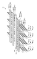
- FIG. 3 is a diagram illustrating an example of a perspective configuration of the memory cell array in FIG. 2.
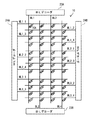
- FIG. 3 is a diagram illustrating an example of an equivalent circuit of the memory cell array in FIG. 2.
- FIG. 4 is a diagram illustrating an example of a cross-sectional configuration of the memory cell of FIG. 3.
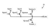
- FIG. 3 is a diagram illustrating an example of a circuit configuration of a BL driver circuit in FIG. 2.
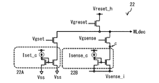
- FIG. 3 is a diagram illustrating an example of a circuit configuration of a WL driver circuit in FIG. 2.
- FIG. 2 is a diagram illustrating an example of functional blocks of the memory cell array unit in FIG. 1.
- FIG. 3 is a diagram illustrating an example of a perspective configuration of the memory cell array in FIG. 2.
- FIG. 3 is a diagram illustrating an example of an equivalent circuit of the memory cell array in FIG. 2.
- FIG. 4 is a diagram illustrating
- FIG. 3 is a diagram illustrating an example of a circuit configuration of a precharge circuit in FIG. 2.
- FIG. 3 is a diagram illustrating an example of a circuit configuration of a BL decoder and a WL decoder in FIG. 2.
- 10 is a truth table of the BL decoder and WL decoder of FIG. 9. It is a figure showing an example of the circuit structure of the decoder which concerns on a comparative example.
- 12 is a truth table of decoding in the BL decoder and WL decoder of FIG. It is a figure showing an example of the voltage applied to a memory cell array at the time of precharge. It is a figure showing an example of the voltage applied to a memory cell array at the time of floating.
- FIG. 8 is a diagram illustrating a modification example of functional blocks of the memory cell array unit in FIG. 1.
- FIG. 21 is a diagram illustrating an example of a circuit configuration of a Vcom circuit in FIG. 20. It is a figure showing an example of the voltage waveform in the memory cell of writing object. It is a figure showing the modification of the voltage waveform in the memory cell of writing object. It is a figure showing an example of the voltage waveform in the memory cell of reset object. It is a figure showing an example of the voltage waveform in the memory cell of reading object.
- FIG. 21 is a diagram illustrating a modification of the circuit configuration of the BL driver circuit of FIGS. 2 and 20.
- FIG. 21 is a diagram illustrating a modification of the circuit configuration of the WL driver circuit of FIGS. 2 and 20.
- FIG. 21 is a diagram illustrating a modification of the circuit configuration of the precharge circuit in FIGS. 2 and 20.
- FIG. 21 is a diagram illustrating a modification of the perspective configuration of the memory cell array in FIGS. 2 and 20.
- FIG. 32 is a diagram illustrating an example of an equivalent circuit of the memory cell array in FIG. 31.
- FIG. 1 illustrates an example of functional blocks of an information processing system according to an embodiment of the present disclosure.
- This information processing system includes a host computer 100 and a memory system 200.
- the memory system 200 includes a memory controller 300, one or a plurality of memory cell array units 400, and a power supply circuit 500.
- FIG. 1 illustrates a state where a plurality of memory cell array units 400 are provided.
- the memory system 200 corresponds to a specific example of “memory system” of the present disclosure.
- the memory controller 300 corresponds to a specific example of “memory controller” of the present disclosure.
- the memory cell array unit 400 corresponds to a specific example of “memory device” of the present disclosure.
- the host computer 100 controls the memory system 200. Specifically, the host computer 100 issues a command designating an access destination logical address, and supplies the command and data to the memory system 200. In addition, the host computer 100 receives the data output from the memory system 200.
- the command is for controlling the memory system 200 and includes, for example, a write command for instructing a data write process or a read command for instructing a data read process.
- the logical address is an address allocated for each area of the access unit when the host computer 100 accesses the memory system 200 in the address space defined by the host computer 100. Hereinafter, this access unit area is referred to as a “sector”.
- the size of each sector is, for example, 4 KB (kilobyte).
- the memory controller 300 controls one or a plurality of memory cell array units 400.
- the memory controller 300 receives a write command specifying a logical address from the host computer 100. Further, the memory controller 300 executes data write processing in accordance with the write command. In this writing process, the logical address is converted to a physical address, and data is written to the physical address.
- the physical address is an address allocated in one or a plurality of memory cell array units 400 for each access unit when the memory controller 300 accesses one or a plurality of memory cell array units 400.
- the unit in which the memory controller 300 accesses one or a plurality of memory cell array units 400 is assumed to be the same as, for example, a sector.
- a physical address is assigned to each sector.
- the memory controller 300 receives a read command designating a logical address
- the memory controller 300 converts the logical address into a physical address, and reads data from the physical address. Then, the memory controller 300 outputs the read data to the host computer 100 as read data.
- the memory controller 300 receives a reset command designating a logical address from the host computer 100
- the memory controller 300 converts the logical address into a physical address and erases the data written in the physical address.
- the access unit by the memory controller 300 may be the same as the access unit by the host computer 100 or may be different. Note that a method for controlling one or a plurality of memory cell array units 400 by the memory controller 300 will be described in detail later.
- the power supply circuit 500 supplies a desired voltage to one or a plurality of memory cell array units 400. Specifically, the power supply circuit 500 supplies a set voltage Vset1, a set voltage Vset2, a sense voltage Vsense_h, and a reset voltage Vreset_i to the BL driver 21 described later. The power supply circuit 500 supplies a ground voltage Vss, a sense voltage Vsense_i, and a reset voltage Vreset_h to the WL driver 22 described later. The power supply circuit 500 supplies a ground voltage Vss and a reference voltage Vcom to a precharge circuit 25 described later. The ground voltage Vss and the sense voltage Vsense_i correspond to a specific example of “first voltage” of the present disclosure. The set voltage Vset1, the set voltage Vset2, and the sense voltage Vsense_h correspond to a specific example of “third voltage” of the present disclosure.
- the set voltage Vset1 is a voltage that can apply a voltage equal to or higher than the voltage Vsnap at which the switching element 10S changes from the high resistance state to the low resistance state to the switching element 10S.
- the set voltage Vset2 is a voltage lower than the set voltage Vset1.
- the set voltage Vset2 is a voltage lower than the voltage Vsnap and is a voltage large enough to maintain the current Iset that is large enough to write to the memory cell 10A. is there.
- the resistance of the memory element 10M when writing into the memory cell 10A is started is Rhrs.
- a voltage at which the switching element 10S changes from the low resistance state to the high resistance state is represented by Vhold.
- the set voltage Vset1 is a voltage higher than (voltage Vsnap + current Iset ⁇ resistance Rhrs).
- the set voltage Vset2 is a voltage higher than (voltage Vhold + current Iset ⁇ resistance Rhrs).
- the sense voltage Vsense_h is higher than the ground voltage Vss and lower than the set voltage Vset2.
- the sense voltage Vsense_h is a voltage higher than the sense voltage Vsense_i.
- the reset voltage Vreset_h is higher than the reset voltage Vreset_i.
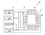
- FIG. 2 shows an example of functional blocks of the memory cell array unit 400.
- the memory cell array unit 400 is constituted by, for example, a semiconductor chip.
- the memory cell array unit 400 includes the memory cell array 10 and the control circuit 20.
- the control circuit 20 exchanges commands, write data, read data, and the like with the memory controller 300.
- the control circuit 20 writes data to the memory cell array 10 according to the write command, and reads data from the memory cell array 10 according to the read command. Further, the control circuit 20 erases data at a predetermined location in the memory cell array 10 in accordance with the reset command.
- the control circuit 20 will be described in detail later.
- FIG. 3 illustrates an example of a perspective configuration of the memory cell array 10.
- the memory cell array 10 has n (n is an integer of 2 or more) sectors. Each sector has a plurality of memory cells 10A corresponding to the sector size. A physical address is assigned to each sector.
- the memory cell array 10 includes a plurality of word lines WL, a plurality of bit lines BL, and a plurality of memory cells 10A arranged one at each position where the word lines WL and the bit lines BL face each other. Yes.
- the word line WL corresponds to a specific example of “row wiring” of the present disclosure.
- the bit line BL corresponds to a specific example of “column wiring” of the present disclosure.
- position information (1_1, 1_2, etc.) is added to the end of the code of each word line WL, and position information (1, 2, 3, 3) is also added to the end of the code of each bit line BL. 4).
- position information of 1_1, 1_2, 1_3, and 1_4 is given to the four word lines WL provided in the first layer.
- positional information of 2_1, 2_2, 2_3, 2_4 is given to the four word lines WL provided in the second layer, and for the four word lines WL provided in the third layer, Position information 3_1, 3_2, 3_3, and 3_4 is given.
- position information 1_1, 2_1, 3_1 is assigned to the word line WL in the first row
- position information 1_2, 2_2, 3_2 is assigned to the word line WL in the second row
- Position information 1_3, 2_3, and 3_3 is assigned to the word line WL in the third row
- position information 1_4, 2_4, and 3_4 is assigned to the word line WL in the fourth row.
- 1 position information is given to the bit line BL, horizontal bit line HBL and vertical bit line VBL in the first column, and to the bit line BL, horizontal bit line HBL and vertical bit line VBL in the second row.
- position information 2 is given.
- Position information 3 is given to the bit line BL, horizontal bit line HBL, and vertical bit line VBL in the third row, and for the bit line BL, horizontal bit line HBL, and vertical bit line VBL in the fourth row, Position information 4 is assigned.
- the plurality of memory cells 10A are arranged in a matrix.
- a plurality of memory cells 10A are arranged in a matrix on a horizontal plane (two-dimensional, XY plane), and also on a vertical plane (two-dimensional, XZ plane or YZ plane). Arranged in a shape. That is, a plurality of memory cells 10A are stacked. Thereby, a storage device with higher density and larger capacity can be provided.
- the plurality of memory cells 10A have a stacked arrangement as shown in FIG.
- the plurality of word lines WL are arranged in a plurality of layers. Each word line WL extends in the row direction.
- Each bit line BL is composed of a horizontal bit line HBL extending in the column direction and a vertical bit line VBL connected to the horizontal bit line HBL and extending in the vertical direction.
- the plurality of horizontal bit lines HBL are arranged in one layer, and the plurality of vertical bit lines VBL are two word lines WL adjacent to each other in the horizontal plane. It is arranged between.
- the plurality of vertical bit lines VBL and the plurality of word lines WL are arranged to face each other with a predetermined gap in the horizontal plane.
- Each memory cell 10A is sandwiched between vertical bit lines VBL and word lines WL in a horizontal plane. From the above, the memory cell array 10 has a V3D structure.
- FIG. 4 shows an example of an equivalent circuit of the memory cell array 10.
- One memory cell 10A is provided for each portion where each bit line BL and each word line WL face each other.
- a plurality of memory cells 10A connected to the four upper word lines WL1_1 to WL1_4 in FIG. 4 are provided in the first layer.
- a plurality of memory cells 10A connected to the four word lines WL2_1 to WL2_4 in the center of FIG. 4 are provided in the second layer.
- a plurality of memory cells 10A connected to the four word lines WL3_1 to WL3_4 on the lower side of FIG. 4 are provided in the third layer.
- the memory cell array 10 is equivalent to a cross-point memory cell array in which memory cells are arranged at intersections where wirings extending in different directions in a horizontal plane intersect each other. I know that there is.
- FIG. 5 shows an example of a cross-sectional configuration of the memory cell 10A.
- the memory cell 10 has a current path PI including a memory element 10M and a switch element 10S connected in series with each other.
- the memory element 10M corresponds to a specific example of “memory element” of the present disclosure.
- the switch element 10S corresponds to a specific example of “switch element” of the present disclosure.
- the memory element 10M is disposed, for example, near the word line WL, and the switch element 10S is disposed, for example, near the bit line BL (vertical bit line VBL).
- the memory element 10M may be disposed near the bit line BL (vertical bit line VBL), and the switch element 10S may be disposed near the word line WL.
- the memory element 10M when the memory element 10M is disposed near the word line WL and the switch element 10S is disposed near the bit line BL (vertical bit line VBL), in the layer adjacent to the layer, The memory element 10M may be disposed near the bit line BL (vertical bit line VBL), and the switch element 10S may be disposed near the word line WL.
- the memory element 10 ⁇ / b> M includes an electrode 11, an electrode 13 disposed to face the electrode 11, and a memory layer 12 provided between the electrode 11 and the electrode 13.
- the memory layer 12 has, for example, a stacked structure in which a resistance change layer and an ion source layer are stacked, or a single layer structure of a resistance change layer.
- the resistance change layer is constituted by an insulating layer made of, for example, SiN, SiO 2 , Gd 2 O 3 or the like.
- the ion source layer includes a movable element that forms a conduction path in the resistance change layer by application of an electric field.
- the ion source layer is composed of, for example, a metal film containing one or more metal elements selected from Cu, Ag, Zr, and Al, an alloy film (for example, a CuTe alloy film), a metal compound film, and the like. Note that metal elements other than Cu, Ag, Zr, and Al may be used for the ion source layer as long as they have a property of being easily ionized.
- the ion source layer may also be made of a material in which at least one element of Cu, Ag, Zr, and Al and at least one chalcogen element of S, Se, and Te are combined.
- the switch element 10 ⁇ / b> S includes an electrode 15, an electrode 13 that is disposed to face the electrode 15 and also serves as an electrode of the memory element 10 ⁇ / b> M, and a switch layer 14 that is provided between the electrode 15 and the electrode 13.
- the switch layer 14 includes, for example, at least one chalcogen element of S, Se, and Te.
- the switch layer 14 may be configured to further include at least one element of B, Al, Ga, C, Si, Ge, N, P, As, Ab, and Bi in addition to the chalcogen element. preferable.
- the switch layer 14 changes to a low resistance state by raising the applied voltage to a predetermined threshold voltage (switching threshold voltage) or higher, and has a high resistance by lowering the applied voltage to a voltage lower than the above threshold voltage (switching threshold voltage). It changes to a state. That is, in the switch layer 14, the amorphous structure of the switch layer 14 is stably maintained regardless of the application of the voltage pulse or the current pulse via the electrode 15 and the electrode 13. Further, the switch layer 14 does not perform a memory operation such that a conduction path formed by movement of ions by voltage application is maintained even after the applied voltage is erased.
- IV characteristics of memory cell 10A Next, the IV characteristic of the memory cell 10A will be described. Hereinafter, the IV characteristics of the switching element 10S and the memory element 10M constituting the memory cell 10A will be described, and then the IV characteristics of the memory cell 10A will be described.
- the current value increases as the forward bias (write voltage) increases, and a write operation is performed by forming a conduction path in the resistance change layer at a predetermined write voltage (for example, about 3.5 V).
- the memory layer 12 changes to a low resistance state, and the current increases. That is, the memory element 10M is brought into a low resistance state by application of the write voltage, and this low resistance state is maintained even after the application voltage is stopped.
- the current increases with an increase in the write voltage in the switch element 10S, and when the voltage exceeds a predetermined threshold voltage (for example, about 4V), the current rapidly increases due to the OTS operation. Or, the resistance is lowered and the device is turned on. Thereafter, when the write voltage is decreased, the value of the current flowing through the electrode of the switch element 10S gradually decreases. For example, although depending on the material constituting the switch element 10S and the formation conditions, the resistance rapidly increases at a threshold voltage almost equal to that at the time of increase, and the switch element 10 is turned off.
- a predetermined threshold voltage for example, about 4V
- the switching behavior of the current value at the start and stop of application of the write voltage to the memory cell 10A is an IV curve that combines the IV curves of the switch element 10S and the memory element 10M.
- the read voltage (Vread) of the memory cell 10A is set to a voltage larger than the threshold value on the IV curve where the resistance changes rapidly, and Vread / 2 is a resistance.
- a voltage smaller than the change threshold is set. This increases the selection ratio (on / off ratio) defined by the current ratio between the Vread bias and the Vread / 2 bias.
- the IV curve of the memory cell 10A is a combination of the IV curve of the switch element 10S and the IV curve of the memory element 10M.
- the IV curve of the memory cell 10A is a combination of the IV curve of the switch element 10S and the IV curve of the memory element 10M.
- the array size can be increased without erroneous reading, and the capacity of the memory cell array can be further increased. This is the same for the write operation as well as the read operation.
- the change in the current value when the erase voltage is applied to the switch element 10S exhibits the same behavior as when the write voltage is applied.
- the change in the current value when the erase voltage is applied to the memory element 10M changes from the low resistance state to the high resistance state by applying a voltage equal to or higher than the erase threshold voltage (for example, about 2 to 3 V).
- the change in the current value when the erase voltage is applied to the memory cell 10A is a combination of the IV curve of the switch element 10S and the IV curve of the memory element 10M, as in the case of applying the write voltage.
- the control circuit 20 includes a BL driver circuit 21, a WL driver circuit 22, two BL decoders 23A and 23B, two WL decoders 24A and 24B, a precharge circuit 25, and a readout circuit 26.
- the BL driver circuit 21 and the precharge circuit 25 control the voltages applied to the two BL decoders 23A and 23B according to the control by the memory controller 300.
- the WL driver circuit 22 and the precharge circuit 25 control the voltages applied to the two WL decoders 24A and 24B according to the control by the memory controller 300.
- the memory controller 300 controls the BL driver circuit 21, the WL driver circuit 22, and the precharge circuit 25, and controls the BL decoder 23A, the BL decoder 23B, the WL decoder 24A, and the WL decoder 24B independently of each other.
- a circuit including the BL driver circuit 21, the WL driver circuit 22, the precharge circuit 25, and the power supply circuit 500 corresponds to a specific example of “voltage control circuit” of the present disclosure.
- the WL decoder 24A corresponds to a specific example of a “first decoder circuit” of the present disclosure.
- the WL decoder 24B corresponds to a specific example of “second decoder circuit” of the present disclosure.
- the BL decoder 23A corresponds to a specific example of “third decoder circuit” of the present disclosure.
- the BL decoder 23B corresponds to a specific example of “fourth decoder circuit” of the present disclosure.
- FIG. 6 shows an example of the circuit configuration of the BL driver circuit 21.
- the BL driver circuit 21 controls the voltage applied to the two BL decoders 23A and 23B.
- the BL driver circuit 21 selects one voltage from the four types of voltages (Vset1, Vset2, Vsense_h, Vreset_i) supplied from the power supply circuit 500 according to control by the memory controller 300.
- the BL driver circuit 21 outputs the selected voltage to the BL decoders 23A and 23B (specifically, an input terminal drv described later).
- the four types of voltages (Vset1, Vset2, Vsense_h, Vreset_i) correspond to a specific example of “third voltage” of the present disclosure.
- the BL driver circuit 21 selects the set voltage Vse1 or the set voltage Vse2 and outputs it to the BL decoders 23A and 23B during the write operation.
- the BL driver circuit 21 selects the sense voltage Vsense_h and outputs it to the BL decoders 23A and 23B during the read operation.
- the BL driver circuit 21 selects the reset voltage Vreset_i and outputs it to the BL decoders 23A and 23B during the reset operation.
- the memory controller 300 outputs the control signals Vgset1, Vgset2, Vgsense, and Vgreset to the BL driver circuit 21, thereby supplying one voltage from the four types of voltages (Vset1, Vset2, Vsense_h, and Vreset_i) to the BL driver circuit 21. Let them choose.
- the BL driver circuit 21 selects one voltage from the four kinds of voltages (Vset1, Vset2, Vsense_h, Vreset_i) based on the control signals Vgset1, Vgset2, Vgsense, Vgreset from the memory controller 300, and the BL decoder 23A , 23B.
- FIG. 7 shows an example of the circuit configuration of the WL driver circuit 22.
- the WL driver circuit 22 controls the voltage applied to the two WL decoders 24A and 24B.
- the WL driver circuit 22 selects one voltage from the three types of voltages (Vss, Vsense_i, Vreset_h) supplied from the power supply circuit 500 under the control of the memory controller 300.
- the WL driver circuit 22 outputs the selected voltage to WL decoders 24A and 24B (specifically, an input terminal drv described later).
- Three types of voltages (Vss, Vsense_i, Vreset_h) correspond to a specific example of “first voltage” of the present disclosure.
- the WL driver circuit 22 selects the ground voltage Vss and outputs it to the WL decoders 24A and 24B.
- the WL driver circuit 22 selects the sense voltage Vsense_i and outputs it to the WL decoders 24A and 24B.
- the WL driver circuit 22 selects the reset voltage Vreset_h and outputs it to the WL decoders 24A and 24B.
- the memory controller 300 outputs control signals Vgset, Vgsense, and Vgreset to the WL driver circuit 22 to cause the WL driver circuit 22 to select one voltage from among three types of voltages (Vss, Vsense_i, and Vreset_h).
- the WL driver circuit 22 selects one voltage from the three types of voltages (Vss, Vsense_i, Vreset_h) based on the control signals Vgset, Vgsense, and Vgreset from the memory controller 300, and outputs them to the WL decoders 24A and 24B. To do.
- the WL driver circuit 22 further limits the current flowing through the selected word line WL to a predetermined current value (Iset_c) when the ground voltage Vss is selected. Specifically, the WL driver circuit 22 applies the ground voltage Vss to the selected word line WL when the current flowing through the selected word line WL is less than Iset_c. When the current flowing through the selected word line WL is equal to or higher than Iset_c, the WL driver circuit 22 has a voltage higher than the ground voltage Vss so that the current flowing through the selected word line WL exceeds Iset_c. Is output. In this way, by limiting the current value to Iset_c, characteristic deterioration caused by excessive current flowing through the selected memory cell 10 is suppressed.
- Iset_c a predetermined current value
- the WL driver circuit 22 further limits the current flowing through the selected word line WL to a predetermined current value (Isens_c) when the sense voltage Vsense_i is selected. Specifically, the WL driver circuit 22 applies the sense voltage Vsense_i to the selected word line WL when the current flowing through the selected word line WL is less than Isens_c. When the current flowing through the selected word line WL is equal to or higher than Isens_c, the WL driver circuit 22 outputs a voltage higher than the sense voltage Vsense_i so that the current flowing through the selected word line WL does not exceed Isens_c. In this way, by limiting the current value to Isens_c, characteristic deterioration caused by excessive current flowing through the selected memory cell 10 is suppressed.
- Isens_c a predetermined current value
- FIG. 8 shows an example of the circuit configuration of the precharge circuit 25.
- the precharge circuit 25 controls the voltage applied to the two BL decoders 23A and 23B and the two WL decoders 24A and 24B.
- the precharge circuit 25 is a voltage (voltage A) that is a predetermined magnitude larger than one kind of voltage (Vcom) supplied from the power supply circuit 500 and a predetermined magnitude that is higher than the voltage Vcom, under the control of the memory controller 300.
- Select an output destination of a voltage (voltage B) that is as small as possible.
- the precharge circuit 25 outputs the voltage A and the voltage B to the selected output destination.
- the precharge circuit 25 selects the voltage A as the voltage Vpre_w during the write operation or the read operation, and outputs it to the WL decoders 24A and 24B (specifically, an input terminal com described later).
- the precharge circuit 25 selects the voltage B as the voltage Vpre_b during the write operation or the read operation, and outputs it to the BL decoders 23A and 23B (specifically, an input terminal com described later).
- the precharge circuit 25 selects the voltage B as the voltage Vpre_w and outputs it to the WL decoders 24A and 24B during the reset operation.
- the precharge circuit 25 selects the voltage A as the voltage Vpre_b and outputs it to the BL decoders 23A and 23B.
- the voltage Vpre_w corresponds to a specific example of “second voltage” of the present disclosure.
- the voltage Vpre_b corresponds to a specific example of “fourth voltage” of the present disclosure.
- the voltage Vpre_w is higher than the voltage Vpre_b.
- the voltage Vpre_w and the voltage Vpre_b are set so that the difference between the voltage Vpre_w and the voltage Vpre_b is less than 1/3 of the highest voltage (voltage Vsens_h ⁇ voltage Vsens_i) applied to the memory cell 10A to be selected during the read operation.
- the voltage Vpre_w and the voltage Vpre_b are set so that the difference between the voltage Vpre_w and the voltage Vpre_b is less than 1/3 of the highest voltage (voltage Vset1) applied to the memory cell 10A to be selected during the write operation. .
- the memory controller 300 outputs the control signals Vgcom, Vg0, Vg1, Vg2, and Vg3 to the precharge circuit 25, thereby causing the precharge circuit 25 to select the output destination of two types of voltages (Vpre_w, Vpre_b).
- the precharge circuit 25 selects output destinations of two types of voltages (Vpre_w, Vpre_b) based on the control signals Vgcom, Vg0, Vg1, Vg2, Vg3 from the memory controller 300.
- the precharge circuit 25 selects one voltage (Vpre_b) from two types of voltages (Vpre_w, Vpre_b) based on the control signals Vgcom, Vg0, Vg1, Vg2, and Vg3 from the memory controller 300, Output to WL decoders 24A and 24B.
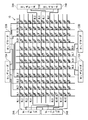
- FIG. 9 shows an example of the circuit configuration of the BL decoders 23A and 23B and the WL decoders 24A and 24B.
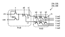
- the BL decoders 23A, 23B and the WL decoders 24A, 24B have, for example, two input terminals drv, com and a plurality of address terminals a0, a1, b0, b1, b2, s.
- the BL decoders 23A and 23B and the WL decoders 24A and 24B have, for example, a plurality of output terminals line0 to line5. In the following, the output terminal line is used as a general term for the output terminals line0 to line5.
- the two input terminals drv and com correspond to a specific example of “two first voltage input terminals” or “two second voltage input terminals” of the present disclosure.
- the plurality of address terminals a0, a1, b0, b1, b2, and s correspond to a specific example of “a plurality of first address input terminals” or “a plurality of second address input terminals” of the present disclosure.
- the input terminal drv is connected to the output terminal BLdec of the BL driver circuit 21, and the input terminal com is connected to the output terminal BLdec of the precharge circuit 25.
- the input terminal drv is connected to the output terminal WLdec of the WL driver circuit 22, and the input terminal com is connected to the output terminal BLdec of the precharge circuit 25.
- a plurality of address terminals a0, a1, b0, b1, b2, and s are connected to the output terminal of the memory controller 300.
- each output terminal line is connected to a different bit line BL one by one. Specifically, in the BL decoder 23A, each output terminal line is connected to the bit line BL in each odd column. In the BL decoder 23B, each output terminal line is connected to each even-numbered bit line BL. In the WL decoders 24A and 24B, each output terminal line is connected to a different word line WL one by one. Specifically, in the WL decoder 24A, each output terminal line is connected to each odd-numbered word line WL. In the WL decoder 24B, each output terminal line is connected to a word line WL in each even row.
- the BL decoders 23A and 23B decode the column addresses input to the plurality of address terminals a0, a1, b0, b1, b2, and s, so that the plurality of bit lines BL and the two input terminals drv and com Set the connection mode.
- the WL decoders 24A and 24B decode the row addresses input to the plurality of address terminals a0, a1, b0, b1, b2, and s, so that the plurality of word lines WL and the two input terminals drv and com Set the connection mode.
- the memory controller 300 generates a row address and outputs it to the WL decoders 24A and 24B, and also generates a column address and outputs it to the BL decoders 23A and 23B.
- the BL decoders 23A and 23B and the WL decoders 24A and 24B are composed of, for example, a predecoder PreD and a post decoder PstD.
- the predecoder PreD selects one of the two input terminals drv and com based on a control signal input from the memory controller 300 to the terminal s.
- the predecoder PreD further sets a connection mode between the selected input terminal and the two wirings L1 and L2 based on a control signal input from the memory controller 300 to the terminals a0 and a1.
- the post decoder PstD sets a connection mode between the two wirings L1 and L2 and the plurality of output terminals line0 to line5 based on a control signal input from the memory controller 300 to the terminals b0, b1, and b2.
- the post decoder PstD has a plurality of switching elements Tr provided for each of the output terminals line0 to line5 by the number of output terminals line0 to line5 of the postdecoder PstD.
- the switch element Tr is composed of, for example, an NMOS transistor.
- the post decoder PstD has a plurality of switch elements Tr provided for each bit line BL by the number of bit lines BL allocated to the post decoder PstD.
- the post decoder PstD has a plurality of switch elements Tr provided for each word line WL by the number of word lines WL assigned to the post decoder PstD.
- the post decoder PstD is provided with one switching element Tr dedicated to one output terminal line, which is not shared with other output terminals line, for each wiring line.
- a decoder in which the post decoder PstD has such a configuration is called a 1T decoder.
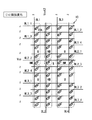
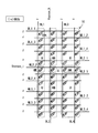
- FIG. 10 is a truth table of the BL decoders 23A and 23B and the WL decoders 24A and 24B.
- the WL decoders 24A and 24B change the connection mode between the input terminals drv and com and the output terminals line0 to line5 based on the row addresses input from the memory controller 300 to the terminals a0, a1, b0, b1, b2, and s. As shown in the truth table of FIG.
- the BL decoders 23A and 23B change the connection mode between the input terminals drv and com and the output terminals line0 to line5 based on the column addresses input from the memory controller 300 to the terminals a0, a1, b0, b1, b2, and s. As shown in the truth table of FIG. As shown in the truth table of FIG. 10, among the output terminals line0 to line5, all of the output terminals except the floating output terminal have only one of the input terminals drv and com. Conduct.
- 0 means a low voltage (Low)
- 1 means a tournament voltage (High). Therefore, the switch element to which “0” is input is turned off (non-conducting), and the switch element to which “1” is input is turned on (conducting).
- z means a floating state
- drv means a conduction state with the input terminal drv
- com a conduction state with the input terminal com. Means.
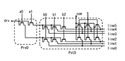
- FIG. 11 shows an example of a circuit configuration of a decoder according to a comparative example.
- FIG. 12 is a truth table of the decoder according to the comparative example.
- the decoder according to the comparative example has, for example, two input terminals drv, com and a plurality of address terminals a0, a1, b0, b1, b2, s.
- the decoder according to the comparative example has, for example, a plurality of output terminals line0 to line5. That is, the decoder according to the comparative example has the same configuration as the BL decoders 23A and 23B and the WL decoders 24A and 24B in these respects.
- the post-decoder PstD of the decoder according to the comparative example, two switching elements dedicated to one output terminal line, which are not shared with other output terminals line, are provided for each wiring line.
- a decoder in which the post decoder PstD has such a configuration is called a 2T decoder.
- One switch element is used for setting a connection mode between the input terminal drv provided in the predecoder PreD and the output terminals line0 to line5.
- the other switch element is used for setting a connection mode between the input terminal com provided in the post decoder PstD and the output terminals line0 to line5.
- the decoder according to the comparative example outputs two types of voltages (except for the floating state) to the output terminals line0 to line5 with a configuration called a 2T decoder.
- the BL decoders 23A and 23B and the WL decoders 24A and 24B output one type of voltage (except for the floating state) to the output terminals line0 to line5 by a configuration called a 1T decoder. Therefore, in the BL decoders 23A and 23B and the WL decoders 24A and 24B, the circuit area of the post decoder PstD is smaller by a smaller number of switch elements in the post decoder PstD than in the decoder according to the comparative example.
- the read circuit 26 reads data written in the memory cell array 10 under the control of the memory controller 300.
- the read circuit 26 has, for example, a sense amplifier connected to each output terminal line of the WL decoders 24A and 24B.
- the read circuit 26 detects the voltage of each output terminal line of the WL decoders 24 ⁇ / b> A and 24 ⁇ / b> B with a sense amplifier during a read operation, and outputs the detected result to the memory controller 300.
- FIG. 13A shows an example of a voltage applied to the memory cell array 10 during precharging.
- FIG. 13B shows an example of a voltage applied to the memory cell array 10 during floating.
- FIG. 13C shows an example of a voltage applied to the memory cell array 10 at the time of writing.
- FIG. 13D shows an example of a voltage applied to the memory cell array 10 after writing.
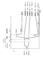
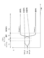
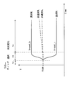
- FIG. 14 shows an example of a voltage waveform in the memory cell 10A to be written.
- the memory system 200 executes the write operation in the order of (i) precharge, (ii) floating, (iii) selection, and (iv) resistance change.
- the memory controller 300 outputs a row address (third row address) for connecting each word line WL to the input terminals drv of the WL decoders 24A and 24B to the WL decoders 24A and 24B.
- the memory controller 300 further outputs a column address (third column address) for connecting the voltage of each bit line BL to the input terminal drv of the BL decoders 23A and 23B to the BL decoders 23A and 23B. Then, all the bit lines BL and all the word lines WL are connected to the precharge circuit 25.
- the memory controller 300 further outputs a control signal for outputting a voltage (voltage A) larger than the voltage Vcom by a predetermined magnitude to the WL decoders 24A and 24B as the voltage Vpre_w to the precharge circuit 25.
- the memory controller 300 further outputs to the precharge circuit 25 a control signal for outputting a voltage (voltage B) smaller than the voltage Vcom by a predetermined magnitude as the voltage Vpre_b to the BL decoders 23A and 23B.
- the memory controller 300 sets Vgcom of the precharge circuit 25 to High, sets the voltage of each bit line BL and each word line WL to Vgcom, and then sets Vgcom of the precharge circuit 25 to Low.
- the memory controller 300 sets Vg0 and Vg1 of the precharge circuit 25 to High and sets Vg2 and Vg3 to Low. Then, a part of the electric charge charged in the bit line BL moves to the capacitor Cpump, and the voltage of the bit line BL decreases.
- the memory controller 300 sets Vg0 and Vg1 of the precharge circuit 25 to Low and Vg2 and Vg3 to High.
- the memory controller 300 causes each word line WL and each bit line BL to be in a floating state with respect to a decoder (for example, WL decoder 24A and BL decoder 23B) connected to the memory cell 10A to be selected.
- the row address and column address to be output are output.
- the memory controller 300 sets all the address terminals a0, a1, b1, b2, b3, and s of the WL decoder 24A and the BL decoder 23B to Low.
- each word line WL and each bit line BL connected to the WL decoder 24A and the BL decoder 23B are in a floating state (period T2 in FIGS. 13B and 14).
- the memory controller 300 outputs the first row address as a row address to a decoder (for example, the WL decoder 24A) connected to the memory cell 10A to be selected.
- the memory controller 300 further outputs the second row address as a row address to a decoder (for example, the WL decoder 24B) not connected to the memory cell 10A to be selected.
- the first row address connects the word line WL (for example, WL2_2) connected to the memory cell 10A to be selected to the input terminal drv of the WL decoder 24A and is not connected to the memory cell 10A to be selected. Is a row address for bringing each word line WL into a floating state.
- the second row address is a word line WL (for example, WL2_1, WL2_3) adjacent to at least the word line WL (for example, WL2_2) connected to the memory cell 10A to be selected among the plurality of word lines WL. , WL1_2, WL3_2) are connected to the input terminal drv of the WL decoder 24B.
- the memory controller 300 further outputs the first column address as a column address to a decoder circuit (for example, the BL decoder 23B) connected to the memory cell 10A to be selected.
- the memory controller 300 further outputs the second column address as a column address to a decoder circuit (for example, the BL decoder 23A) not connected to the memory cell 10A to be selected.
- the first column address connects the bit line BL (for example, BL2) connected to the memory cell 10A to be selected to the input terminal drv of the BL decoder 23B and is not connected to the memory cell 10A to be selected.
- the second column address is a bit line BL (for example, BL1, BL3) adjacent to at least the bit line BL (for example, BL2) connected to the memory cell 10A to be selected among the plurality of bit lines BL. ) Is a column address connecting the BL decoder 23A to the input terminal drv.
- the memory controller 300 further outputs to the WL driver 22 a control signal for outputting the voltage Vss to the WL decoders 24A and 24B. For example, the memory controller 300 sets Vgset of the WL driver 22 to High and sets Vgreset and Vgsense of the WL driver 22 to Low. The memory controller 300 further outputs a control signal for outputting the voltage Vset1 to the BL decoders 23A and 23B to the BL driver 21. For example, the memory controller 300 sets Vgset 1 of the BL driver 21 to High, and sets Vgset 2, Vgreset, and Vgsense of the BL driver 21 to Low.
- the set voltage is a voltage large enough to apply a voltage equal to or higher than the write threshold voltage at which the memory element 10M changes from the high resistance state to the low resistance state to the memory element 10M in the selected memory cell S. .
- a decoder for example, the BL decoder 23A and the WL decoder 24A connected to the half-selected memory cell HW has a voltage Vpre_b ⁇ voltage. Vss is applied.
- a decoder for example, a BL decoder 23B and a WL decoder 24B connected to the half-selected memory cell HB has a voltage Vset1-voltage. Vpre_w is applied. Thus, the set voltage is applied to the selected memory cell S.
- the resistance of the selected memory cell S starts to decrease from the high resistance. Furthermore, a fixed voltage that is smaller than the set voltage and small enough not to cause a resistance change in the memory cell 10A is applied to each half-selected memory cell HW and each half-selected memory cell HB adjacent to the selected memory cell S. .
- the memory controller 300 floats each word line WL and each bit line BL with respect to a decoder (for example, WL decoder 24B and BL decoder 23A) not connected to the memory cell 10A to be selected.
- the row address and column address to be set are output.
- the memory controller 300 sets all the address terminals a0, a1, b1, b2, b3, and s of the WL decoder 24B and the BL decoder 23A to Low.
- each word line WL and each bit line BL connected to the WL decoder 24B and the BL decoder 23A are in a floating state (FIG. 13D).
- the memory controller 300 further outputs a control signal for changing the voltage output to the BL decoders 23A and 23B from the voltage Vset1 to the voltage Vset2 to the BL driver 21.
- the memory controller 300 sets Vgset1, Vgreset, and Vgsense of the BL driver 21 to Low, and sets Vgset2 of the BL driver 21 to High.
- the voltage Vset2 ⁇ the voltage Vss is applied to the memory cell 10A (selected memory cell S) to be selected (period T4 in FIGS. 13D and 14).
- the resistance of the selected memory cell S further decreases from the high resistance state, and becomes a low resistance state.
- the voltage transitions of the non-selected word line WL (non-selected WL) and the non-selected bit line BL (non-selected BL) are drawn with dotted lines. It shows that at least some of them are in a floating state. Parasitic capacitances exist between the word lines WL, between the bit lines BL, and between the word lines WL and the bit lines BL. In the unselected word line WL in the floating state, a current flows from the selected bit line BL through the half-selected memory cell. In addition, a current flows to the non-selected bit line BL through the non-selected memory cell. Therefore, the parasitic capacitance is charged and discharged by each current, and the voltage of the unselected word line WL in the floating state varies. The same applies to the non-selected bit line BL in the floating state.
- each current varies depending on the voltage of the selected bit line BL and the selected word line WL and the state of the non-selected memory cell (whether it is in a high resistance state or a low resistance state).
- the voltages of the unselected bit lines BL and the unselected word lines WL drawn with dotted lines gradually decrease at “(iv) resistance change”.
- the voltage of the non-selected bit line BL and the non-selected word line WL drawn with lines may rise at “(iv) resistance change”.
- variations in voltage may occur such that the voltage of a certain unselected word line WL increases and the voltage of another unselected word line WL decreases.
- a line labeled “(IwI ⁇ Iset_c)” indicates each voltage transition when the current IwI flowing through the selected word line WL is less than Iset_c.
- FIG. 15 is a diagram illustrating another example of a voltage waveform in the memory cell 10A to be written.
- the memory controller 300 uses (iv) a control signal for using the voltage Vset1 instead of the voltage Vset2 as the voltage to be output to the BL decoders 23A and 23B to the BL driver 21 in the resistance change. May be output.
- FIG. 16A shows an example of a voltage applied to the memory cell array 10 at the time of reset.
- FIG. 16B shows an example of a voltage applied to the memory cell array 10 after reset.
- FIG. 17 shows an example of a voltage waveform in the memory cell 10A to be written.
- the reset operation precharge and (ii) floating, an example of a voltage applied to the memory cell array 10 is the same as in FIGS. 13A and 13B.
- the memory system 200 executes the reset operation in the order of (i) precharge, (ii) floating, (iii) selection, and (iv) resistance change.
- the memory controller 300 outputs a row address (third row address) for connecting each word line WL to the input terminals drv of the WL decoders 24A and 24B to the WL decoders 24A and 24B.
- the memory controller 300 further outputs a column address (third column address) for connecting the voltage of each bit line BL to the input terminal drv of the BL decoders 23A and 23B to the BL decoders 23A and 23B. Then, all the bit lines BL and all the word lines WL are connected to the precharge circuit 25.
- the memory controller 300 further outputs a control signal for outputting to the WL decoders 24A and 24B a voltage (voltage B) smaller than the voltage Vcom by a predetermined magnitude as the voltage Vpre_w to the precharge circuit 25.
- the memory controller 300 further outputs to the precharge circuit 25 a control signal for outputting a voltage (voltage A) larger than the voltage Vcom by a predetermined magnitude as the voltage Vpre_b to the BL decoders 23A and 23B.
- the memory controller 300 sets Vgcom of the precharge circuit 25 to High, sets the voltage of each bit line BL and each word line WL to Vgcom, and then sets Vgcom of the precharge circuit 25 to Low.
- the memory controller 300 sets Vg3 and Vg1 of the precharge circuit 25 to High and sets Vg2 and Vg0 to Low. Then, a part of the charge charged in the word line WL moves to the capacitor Cpump, and the voltage of the word line WL decreases.
- the memory controller 300 sets Vg3 and Vg1 of the precharge circuit 25 to Low and Vg2 and Vg0 to High.
- the memory controller 300 causes each word line WL and each bit line BL to be in a floating state with respect to a decoder (for example, WL decoder 24A and BL decoder 23B) connected to the memory cell 10A to be selected.
- the row address and column address to be output are output.
- the memory controller 300 sets all the address terminals a0, a1, b1, b2, b3, and s of the WL decoder 24A and the BL decoder 23B to Low.
- each word line WL and each bit line BL connected to the WL decoder 24A and the BL decoder 23B are in a floating state (period T2 in FIGS. 13B and 17).
- the memory controller 300 outputs the first row address as a row address to a decoder (for example, the WL decoder 24A) connected to the memory cell 10A to be selected.
- the memory controller 300 further outputs the second row address as a row address to a decoder (for example, the WL decoder 24B) not connected to the memory cell 10A to be selected.
- the memory controller 300 further outputs the first column address as a column address to a decoder circuit (for example, the BL decoder 23B) connected to the memory cell 10A to be selected.
- the memory controller 300 further outputs the second column address as a column address to a decoder circuit (for example, the BL decoder 23A) not connected to the memory cell 10A to be selected.
- the memory controller 300 further outputs to the WL driver 22 a control signal for outputting the voltage Vreset_h to the WL decoders 24A and 24B. For example, the memory controller 300 sets Vgset and Vgsense of the WL driver 22 to Low and Vgreset of the WL driver 22 to High. The memory controller 300 further outputs a control signal for outputting the voltage Vreset_i to the BL decoders 23A and 23B to the BL driver 21. For example, the memory controller 300 sets Vgset1, Vgset2, and Vgsense of the BL driver 21 to Low, and sets Vgset of the BL driver 21 to High.
- a decoder for example, BL decoder 23B and WL decoder 24A connected to the memory cell 10A (selected memory cell S) to be selected outputs the voltage Vreset_h and the voltage Vreset_i.
- the reset voltage is a voltage large enough to apply a voltage equal to or higher than the erase threshold voltage at which the memory element 10M changes from the low resistance state to the high resistance state to the memory element 10M in the selected memory cell S. .
- a decoder for example, the BL decoder 23A and the WL decoder 24A connected to the half-selected memory cell HW has a voltage Vpre_b ⁇ voltage.
- Vreset_h is applied.
- a decoder for example, a BL decoder 23B and a WL decoder 24B connected to the half-selected memory cell HB has a voltage Vreset_i ⁇ voltage. Vpre_w is applied.
- the reset voltage is applied to the selected memory cell S.
- the resistance of the selected memory cell S rises from a low resistance and enters a high resistance state. Furthermore, a fixed voltage that is smaller than the reset voltage and small enough not to cause a resistance change in the memory cell 10A is applied to each half-selected memory cell HW and each half-selected memory cell HB adjacent to the selected memory cell S. .
- the memory controller 300 floats each word line WL and each bit line BL with respect to a decoder (for example, WL decoder 24B and BL decoder 23A) not connected to the memory cell 10A to be selected.
- the row address and column address to be set are output.
- the memory controller 300 sets all the address terminals a0, a1, b1, b2, b3, and s of the WL decoder 24B and the BL decoder 23A to Low.
- each word line WL and each bit line BL connected to the WL decoder 24B and the BL decoder 23A are in a floating state (FIG. 16B).
- FIG. 18A shows an example of a voltage applied to the memory cell array 10 at the time of reading.
- FIG. 18B shows an example of a voltage applied to the memory cell array 10 after reading.
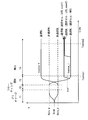
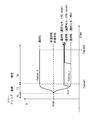
- FIG. 19 shows an example of a voltage waveform in the memory cell 10A to be read. Note that (i) precharge and (ii) floating in the read operation are the same as (i) precharge and (ii) floating in the write operation.
- the memory system 200 executes a read operation in the order of (i) precharge, (ii) floating, (iii) selection, and (iv) detection.
- the memory controller 300 performs a procedure similar to (i) precharge and (ii) floating in the write operation, and then sends it to a decoder (for example, WL decoder 24A) connected to the memory cell 10A to be selected.
- the first row address is output as a row address.
- the memory controller 300 further outputs the second row address as a row address to a decoder (for example, the WL decoder 24B) not connected to the memory cell 10A to be selected.
- the memory controller 300 further outputs the first column address as a column address to a decoder circuit (for example, the BL decoder 23B) connected to the memory cell 10A to be selected.
- the memory controller 300 further outputs the second column address as a column address to a decoder circuit (for example, the BL decoder 23A) not connected to the memory cell 10A to be selected.
- the memory controller 300 further outputs a control signal for outputting the voltage Vsense_i to the WL decoders 24A and 24B to the WL driver 22. For example, the memory controller 300 sets Vgset and Vgreset of the WL driver 22 to Low and Vgsense of the WL driver 22 to High. The memory controller 300 further outputs a control signal for outputting the voltage Vsense_h to the BL decoders 23A and 23B to the BL driver 21. For example, the memory controller 300 sets Vgset1, Vgset2, and Vgreset of the BL driver 21 to Low and sets Vgsense of the BL driver 21 to High.
- decoders for example, the BL decoder 23B and the WL decoder 24A connected to the memory cell 10A (selected memory cell S) to be selected output the voltage Vsense_i and the voltage Vsense_h.
- the voltage Vsense_i the voltage Vsense_h Is applied (period T3 in FIG. 18A and FIG. 19).
- the sense voltage is a voltage large enough to apply a voltage smaller than the write threshold voltage at which the memory element 10M changes from the high resistance state to the low resistance state to the memory element 10M in the selected memory cell S.
- the voltage is higher than the voltage at which the switch element 10S is turned off and is sufficiently large to be applied to the switch element 10S in the selected memory cell S.
- a decoder for example, the BL decoder 23A and the WL decoder 24A connected to the half-selected memory cell HW has a voltage Vpre_b ⁇ voltage. Apply Vse ⁇ BR> ⁇ tang ⁇ Qi.
- a decoder for example, BL decoder 23B and WL decoder 24B connected to the half-selected memory cell HB has a voltage Vsense_h ⁇ voltage. Vpre_w is applied.
- the sense voltage is applied to the selected memory cell S.
- the resistance of the selected memory cell S remains low or high.
- a small fixed voltage that is lower than the set voltage and does not select the memory cell 10A is applied to each half-selected memory cell HW and each half-selected memory cell HB adjacent to the selected memory cell S.
- the memory controller 300 causes each word line WL and each bit line BL to be in a floating state with respect to a decoder (for example, WL decoder 24B and BL decoder 23A) not connected to the memory cell 10A to be selected.
- the row address and column address to be output are output.
- the memory controller 300 sets all the address terminals a0, a1, b1, b2, b3, and s of the WL decoder 24B and the BL decoder 23A to Low.
- each word line WL and each bit line BL connected to the WL decoder 24B and the BL decoder 23A are in a floating state (FIG. 18B).
- the sense voltage applied to the selected memory cell S is smaller than the set voltage, it is considered that there is a low possibility that an unintended resistance change occurs even if a voltage fluctuation occurs during the write operation. Therefore, in the read operation, the sense voltage given by “(iii) selection” is maintained even in the process of “(iv) detection”.
- the current mirror circuit 22B limits the current flowing through the selected word line WL to the specified current value “Isec_c” in “(iii) selection”. Specifically, when the current flowing through the selected word line WL is less than Isec_c, Vsense_i is applied to the selected word line WL, and as a result, the current flowing through the selected word line WL reaches Isec_c. In this case, the current mirror circuit 22B increases the voltage of the selected word line WL so that the current does not exceed Isec_c.
- Isec_c is set to a value sufficiently lower than the current passed through the selected memory cell S in the “(iv) resistance change” step during the write operation so that the resistance of the selected memory cell S is not changed. The That is, Isense_c is smaller than Isec_c.
- the switch element 10S of the selected memory cell S When the switch element 10S of the selected memory cell S is in a low resistance state, when a sense voltage is applied to the selected memory cell S, the current flowing through the selected memory cell S reaches Isense_c, and the selected word line WL The voltage rises.
- the selection WL selected cell: LRS, case1 line of FIG. 19
- the voltage rise of the selected word line WL occurs rapidly in the “(iii) selection” process, as shown in FIG.
- the line of the selected WL selected cell: LRS, case2
- the selected WL selected cell: LRS, case2 in FIG.
- a voltage drop occurs in the selected bit line BL and the selected word line WL due to the current flowing in the memory cell in the half-selected state, and the selected memory cell This occurs when a sufficient voltage is not applied across S.
- the half-selected memory cell The flowing current is reduced and the voltage drop is reduced, a sufficient voltage is applied to the selected memory cell S and Isense_c flows, and the voltage of the selected word line WL rises.
- a read circuit 26 is also connected to the word line WL.
- the read circuit 26 can determine whether the voltage of the selected word line WL is higher or lower than the reference voltage Vref. In this case, when the voltage of the selected word line WL is higher than the reference voltage Vref, it is determined that the selected memory cell S is in a low resistance state, and the voltage of the selected word line WL is higher than the reference voltage Vref. When it is low, it can be determined that the selected memory cell S is in a high resistance state.
- the line of the selected WL selected cell: LRS, case2
- the reading circuit 26 makes such a determination at the timing of Tsense2 in FIG. 19 rather than the timing of Tsense1 in FIG. It is desirable to do.
- the readout circuit 26 may perform the above determination at the timing of Tsense1 in FIG. At this time, the “(iv) detection” step may be omitted.
- the post-decoder PstD of the decoder shown in FIG. 11 two switch elements dedicated to one output terminal line, which are not shared with other output terminals line, are provided for each wiring line. That is, the decoder described in FIG. 11 is a 2T decoder. Therefore, in the decoder shown in FIG. 11, the circuit area of the post decoder PstD becomes large due to the large number of switch elements in the post decoder PstD.
- the word line WL (selected word line WL) connected to the selection target memory cell S and the word line WL adjacent to the selected word line WL are: Two decoder circuits (decoder circuits 24A and 24B) constituted by circuits independent from each other are connected one by one. Furthermore, in the memory system 200 of the present embodiment, the bit line BL (selected bit line BL) connected to the selection target memory cell S and the bit line BL adjacent to the bit line BL are independent from each other. Two decoder circuits (decoder circuits 23A and 23B) constituted by circuits are connected one by one.
- the voltage output from the decoder circuit 24A and the voltage output from the decoder circuit 24B are made different from each other, whereby the selected word line WL and the word line WL adjacent to the selected word line WL are In contrast, two different voltages can be applied to each other.
- the selected bit line BL and the bit line BL adjacent to the selected bit line BL are In contrast, two different voltages can be applied to each other.
- the selected word line WL and the word line WL adjacent to the selected word line WL are driven by different decoder circuits (decoder circuits 24A and 24B). Further, the selected bit line BL and the bit line BL adjacent to the selected bit line BL are driven by different decoder circuits (decoder circuits 23A and 23B).
- decoder circuits 24A and 24B and decoder circuits 23A and 23B a decoder circuit having one switch element 10S for each wiring may be used, and at least two switches are provided for each wiring. There is no need to use a decoder circuit having elements. Accordingly, it is possible to suppress the influence of capacitive coupling between the wirings while suppressing an increase in the floor area of the decoder circuit.
- FIG. 20 shows a modification of the functional block of the memory cell array unit 400 of the above embodiment.
- the memory cell array unit 400 of this modification is different from the configuration of the memory cell array unit 400 of the above embodiment in that it includes a Vcom circuit 27 instead of the precharge circuit 25. Therefore, in the following, contents related to the Vcom circuit 27 will be mainly described, and other descriptions will be appropriately omitted.
- FIG. 21 shows an example of the circuit configuration of the Vcom circuit 27.
- the Vcom circuit 27 has a function equivalent to the function of the precharge circuit 25 when Low is always applied to the terminals Vg1 and Vg2 in the precharge circuit 25.
- the Vcom circuit 27 outputs one type of voltage (Vcom) supplied from the power supply circuit 500 to the input terminal com of each decoder circuit (decoder circuits 24A and 24B and decoder circuits 23A and 23B) under the control of the memory controller 300.
- Vcom voltage supplied from the power supply circuit 500 to the input terminal com of each decoder circuit (decoder circuits 24A and 24B and decoder circuits 23A and 23B) under the control of the memory controller 300.
- the “(i) precharge” step is not provided, and the write operation, the reset operation, and the read operation are performed from the “(ii) floating” step.
- each decoder circuit (decoder circuit 23A or decoder circuit 23B) outputs the voltage Vcom instead of the voltage Vpre_w and the voltage Vpre_b. That is, each decoder circuit (decoder circuit 23A or decoder circuit 23B) outputs a voltage (voltage Vcom) having the same voltage value.
- each decoder circuit (decoder circuit 23A or decoder circuit 23B) outputs a voltage Vcom instead of the voltage Vpre_w and the voltage Vpre_b. Accordingly, when each decoder circuit (decoder circuit 23A or decoder circuit 23B) repeatedly accesses the memory cell array 10, it is not necessary to perform precharge each time the memory cell array 10 is accessed.
- the decoder circuit 23B while the decoder circuit 23A is accessing the memory cell array 10, the decoder circuit 23B always outputs Vcom to the unselected bit line BL and word line WL. Further, part of the current flowing into and out of the selected bit line BL and word line WL in the floating state from the selected bit line BL and word line WL does not contribute to charging of the parasitic capacitance between the wirings. . Further, a part of the current is between the non-selected bit line BL in the floating state and the non-selected word line WL to which Vcom is applied, or the non-selected word line WL in the floating state, The current flows to the non-selected memory cell 10A connected to the non-selected bit line BL to which Vcom is applied. Therefore, the voltage change that occurs in the non-selected wiring in the floating state is very small compared to the case of the above-described embodiment in which precharging is performed.
- the delay time when each decoder circuit (decoder circuit 23A or decoder circuit 23B) repeatedly accesses the memory cell array 10 can be reduced.
- the amount of current flowing through the half-selected memory cell during application of the access voltage is larger than the amount of current flowing through the half-selected memory cell during application of the access voltage in the above embodiment. Therefore, from the viewpoint of power consumption during application of the access voltage, the above embodiment is superior to this modification.
- a precharge circuit 25 may be provided instead of the Vcom circuit 27.
- the memory controller 300 always outputs Low to the terminals Vg1 and Vg2 of the precharge circuit 25 and uses the precharge circuit 25 as having the same function as the Vcom circuit 27. Also good.
- FIG. 26 shows an example of a writing procedure in the memory system 200 according to this modification.
- the memory controller 300 may perform writing to the selected memory cell S after performing precharge only when writing fails.
- the memory controller 300 omits precharging and performs writing to the memory cell 10A (selected memory cell S) to be selected (step S101). Specifically, the memory controller 300 always outputs Low to the terminals Vg1 and Vg2 of the precharge circuit 25 during the first write operation, and has the same function as the Vcom circuit 27. A charge circuit 25 is used. That is, in the first write operation, the memory controller 300 applies one type of voltage (Vcom) supplied from the power supply circuit 500 to the precharge circuit 25 for each decoder circuit (decoder circuits 24A and 24B and A control signal is outputted so as to be outputted to the input terminal com of the decoder circuits 23A, 23B).
- Vcom voltage
- the precharge circuit 25 applies the voltage Vcom having the same voltage value to each decoder circuit (decoder circuits 24A and 24B and decoder circuits 23A and 23B) according to control by the memory controller 300. Output to the input terminal com.
- the memory controller 300 controls the precharge circuit 25 to output the voltage Vcom having the same voltage value to the input terminal com of each decoder circuit (decoder circuits 24A and 24B and decoder circuits 23A and 23B). As a result, the selected memory cell It is determined whether or not the writing to S is successful (step S102). Specifically, the memory controller 300 determines whether or not the selected memory cell S is in a low resistance state. As a result, when the selected memory cell S is in the low resistance state, the memory controller 300 notifies the host computer 100 that the writing to the selected memory cell S has been successful (step S103).
- the memory controller 300 When the selected memory cell S is in the high resistance state, the memory controller 300 performs precharge and then writes to the selected memory cell S again (step S104). Thereafter, the memory controller 300 determines whether writing to the selected memory cell S is successful. Specifically, the memory controller 300 determines whether or not the selected memory cell S is in a low resistance state (step S105). As a result, when the selected memory cell S is in the low resistance state, the memory controller 300 notifies the host computer 100 that the writing to the selected memory cell S has been successful (step S103). If the selected memory cell S is in the high resistance state, the memory controller 300 notifies the host computer 100 that writing to the selected memory cell S has failed (step S106).
- the precharge is omitted only when writing to the selected memory cell S for the first time. Accordingly, it is possible to reduce the delay time when each decoder circuit (decoder circuit 23A or decoder circuit 23B) repeatedly accesses the memory cell array 10 while suppressing frequent writing failures.
- FIG. 27 shows an example of a write procedure in the memory system 200 according to this modification.
- the memory controller 300 has two different voltage values (voltage Vpre_w, voltage Vpre_b) or voltage values depending on the physical position of the selected memory cell S.
- the precharge circuit 25 may be controlled so as to output voltages equal to each other (voltage Vcom).
- the memory controller 300 first detects the write position of the selected memory cell S (step S201). Next, the memory controller 300 determines whether or not the write position of the selected memory cell S is more than a predetermined distance from the position of each decoder circuit (decoder circuit 23A or decoder circuit 23B) (step S202). If the write position of the selected memory cell S is not more than a prescribed distance from the position of each decoder circuit, the memory controller 300 omits the precharge and performs the write to the selected memory cell S (step S203). ). If the write position of the selected memory cell S is more than a predetermined distance from the position of each decoder circuit, the memory controller 300 performs the write to the selected memory cell S after precharging (step). S204).
- precharging is omitted according to the write position of the selected memory cell S. Accordingly, it is possible to reduce the delay time when each decoder circuit (decoder circuit 23A or decoder circuit 23B) repeatedly accesses the memory cell array 10 while suppressing frequent writing failures.
- [Modification D] 28, 29, and 30 illustrate a modification of the circuit configuration of the precharge circuit 25 according to this modification.
- the precharge circuit 25 may include a precharge circuit for the bit line BL and a precharge circuit for the word line WL separately from each other.
- the precharge circuit shown in FIG. 29 or FIG. 30 may be provided for each of the bit line BL and the word line WL. In this case, the voltage of the bit line BL and the precharge voltage can be controlled independently of each other during precharge.
- FIG. 31 illustrates an example of a perspective configuration of the memory cell array 10 according to the present modification.
- FIG. 32 shows an example of an equivalent circuit of the memory cell array 10 of FIG.
- the plurality of memory cells 10A are stacked.
- a plurality of memory cells 10A may be arranged in a single layer.
- a plurality of vertical bit lines VBL and a plurality of word lines WL may be arranged to face each other with a predetermined gap in the horizontal plane. .
- each memory cell 10A may be sandwiched between vertical bit lines VBL and word lines WL in a horizontal plane, for example, as shown in FIG. That is, in the present modification, the memory cell array 10 may have a V3D structure as in the above-described embodiment and the modification.
- each memory cell 10A is provided in the same layer.
- the memory cell array 10 is equivalent to a cross-point memory cell array when expressed by an equivalent circuit as shown in FIG.
- the switch element used in the precharge circuit 25 is configured by, for example, an NMOS transistor, a PMOS transistor, or the like. Further, for example, in the above-described embodiment and its modifications A to E, the switch element used in the precharge circuit 25 is constituted by a CMOS analog switch in which the source and drain are connected with a pair of NMOS transistor and PMOS transistor. May be.
- the number of decoder circuits in the row direction may be three or more.
- the number of decoder circuits in the column direction may be three or more.
- the WL decoder 24B may be omitted, and the WL decoder 24A may be connected to all the word lines WL.
- the BL decoders 23A and 23b are selected by the selected memory cell S.
- the bit line WL connected to may be selected.
- the reading circuit 26 may be connected to the point C of the WL driver 22 as described in FIG. In such a case, the read circuit 26 can be disconnected from the word line WL by setting Vgsense to Low during a reset operation or a write operation.
- the memory controller 300 instead of setting the terminal Vgcom of the precharge circuit 25 to High and setting the voltage of each bit line BL and each word line WL to the voltage Vcom, The terminals Vg0 and Vg3 of the precharge circuit 25 may be set to High. At this time, in the precharge circuit 25, the switch element connected to the terminal Vgcom may be omitted. Even in this case, by setting the terminals Vg0 and Vg3 of the precharge circuit 25 to High, the voltage of each bit line BL and each word line WL can be made close to Vcom.
- the memory cell array 10 has a V3D structure.
- the memory cell array 10 is equivalent to a cross-point structure when expressed by an equivalent circuit. Therefore, the present disclosure is applicable not only to a memory cell array having a V3D structure but also to a memory cell array having a cross point structure.
- this technique can take the following composition.
- a plurality of memory cells having a current path including a selection element and a variable resistance element connected in series with each other, and arranged in a matrix; A plurality of row wirings extending in a row direction and connected to one end of each of the current paths; A plurality of column wirings extending in a column direction and connected to the other end of each of the current paths; A first decoder circuit connected to the row wiring of each even row; A second decoder circuit connected to the row wiring of each odd row; A third decoder circuit connected to the column wiring of each even column; A fourth decoder circuit connected to the column wiring of each odd column; A voltage control circuit for controlling a voltage applied to the first decoder circuit, the second decoder circuit, the third decoder circuit, and the fourth decoder circuit; A memory system comprising: a controller that controls the voltage control circuit and controls the first decoder circuit, the second decoder circuit, the third decoder circuit, and the fourth decoder circuit independently of each other
- the first decoder circuit and the second decoder circuit each have two first voltage input terminals and a plurality of first address input terminals, and are input to the plurality of first address input terminals.
- a connection mode between the plurality of row wirings and the plurality of first voltage input terminals is set,
- the third decoder circuit and the fourth decoder circuit have two second voltage input terminals and a plurality of second address input terminals, and are input to the plurality of second address input terminals.
- a connection mode between the plurality of column wirings and the plurality of second voltage input terminals is set,
- the first decoder circuit and the second decoder circuit each have a plurality of first switch elements for decoding provided for each row wiring by the number of allocated row wirings
- the third decoder circuit and the fourth decoder circuit have a plurality of second switch elements for the decoding provided for each of the column wirings by the number of the column wirings allocated.
- the voltage control circuit outputs a first voltage and a second voltage to two first voltage input terminals of the first decoder circuit and the second decoder circuit, and outputs a third voltage and a fourth voltage to the first voltage.
- the controller outputs a first row address as the row address to a decoder circuit connected to the memory cell to be selected among the first decoder circuit and the second decoder circuit, The controller further outputs a second row address as the row address to a decoder circuit that is not connected to the memory cell to be selected, of the first decoder circuit and the second decoder circuit,
- the first row address connects the row wiring connected to the memory cell to be selected to the first voltage input terminal from which the first voltage is output, and is not connected to the memory cell to be selected.
- the second row address is a row address for setting a voltage of each row wiring adjacent to the row wiring connected to the memory cell to be selected as the second voltage among the plurality of row wirings.
- the memory system according to any one of (2) to (4). (6)
- the controller outputs a first column address as the column address to a decoder circuit connected to the memory cell to be selected among the third decoder circuit and the fourth decoder circuit,
- the controller further outputs a second column address as the column address to a decoder circuit that is not connected to the memory cell to be selected, among the third decoder circuit and the fourth decoder circuit,
- the first column address connects the column wiring connected to the memory cell to be selected to the second voltage input terminal from which the third voltage is output, and is not connected to the memory cell to be selected.
- the second column address is a column address for setting a voltage of each column wiring adjacent to the column wiring connected to the memory cell to be selected among the plurality of column wirings to the fourth voltage.
- the memory system according to (5) When data is written to the memory cell to be selected, the voltage control circuit has a voltage equal to or higher than a write threshold voltage at which the variable resistance element changes from a high resistance state to a low resistance state in the memory cell to be selected.
- the memory system according to (6) wherein a voltage having a magnitude sufficient to be applied to the variable resistance element is output as the first voltage and the third voltage.
- the voltage control circuit has a voltage sufficient to apply a voltage smaller than the threshold voltage to the variable resistance element in the memory cell to be selected when data of the memory cell to be selected is read. And the first voltage and the third voltage are sufficiently large so that a voltage higher than a voltage at which the selection element is turned off is applied to the selection element in the memory cell to be selected.
- the memory system according to (7).
- the controller assigns, to the first decoder circuit and the second decoder circuit, a third row address that connects each of the row wirings to the first voltage input terminal from which the second voltage is output.
- a third column that outputs as an address and connects the voltage of each of the column wirings to the second voltage input terminal from which the fourth voltage is output to the third decoder circuit and the fourth decoder circuit
- the first row address and the second row address are output to the first decoder circuit and the second decoder circuit
- the third decoder circuit and the second decoder address are output.
- the memory according to any one of (6) to (8), wherein the first column address and the second column address are output to a fourth decoder circuit. system. (10) The memory system according to any one of (6) to (8), wherein the voltage control circuit outputs two types of voltages having different voltage values as the second voltage and the fourth voltage.
- the memory system according to any one of (6) to (8), wherein the voltage control circuit outputs voltages having equal voltage values as the second voltage and the fourth voltage. (12) The controller outputs two kinds of voltages having different voltage values or voltages having the same voltage value as the second voltage and the fourth voltage according to the physical position of the memory cell to be selected.
- the memory system according to any one of (6) to (8), wherein the voltage control circuit is controlled.
- the controller sets a voltage of the column wiring connected to the memory cell to be selected to a voltage smaller than the third voltage after the memory cell to be selected is selected. Is output as the column address.
- the memory system according to any one of (6) to (8).
- a current path including a selection element and a variable resistance element connected in series with each other, and a plurality of memory cells arranged in a matrix and extending in a row direction, and a plurality of rows connected to one end of each of the current paths Wiring and A plurality of column wirings extending in a column direction and connected to the other end of each of the current paths; A first decoder circuit connected to the row wiring of each even row; A second decoder circuit connected to the row wiring of each odd row; A third decoder circuit connected to the column wiring of each even column; A fourth decoder circuit connected to the column wiring of each odd column, The memory device, wherein each of the first decoder circuit, the second decoder circuit, the third decoder circuit, and the fourth decoder circuit
- a plurality of memory cells having a current path including a selection element and a variable resistance element connected in series with each other, and arranged in a matrix; A plurality of row wirings extending in a row direction and connected to one end of each of the current paths; A plurality of column wirings extending in a column direction and connected to the other end of each of the current paths; A first decoder circuit connected to the row wiring of each even row; A second decoder circuit connected to the row wiring of each odd row; A third decoder circuit connected to the column wiring of each even column; A fourth decoder circuit connected to the column wiring of each odd column; A memory control method in a memory device comprising: A memory control method comprising: controlling the first decoder circuit, the second decoder circuit, the third decoder circuit, and the fourth decoder circuit independently of each other.
- the decoder circuit connected to the memory cell to be selected outputs the first voltage to the row wiring connected to the memory cell to be selected. A floating state of each row wiring not connected to the memory cell to be selected; Of the first decoder circuit and the second decoder circuit, at least the row connected to the memory cell to be selected among a plurality of the row wirings from a decoder circuit not connected to the memory cell to be selected. Outputting the second voltage to each of the row wirings adjacent to the wiring; Among the third decoder circuit and the fourth decoder circuit, the decoder circuit connected to the memory cell to be selected outputs the third voltage to the column wiring connected to the memory cell to be selected.
- (18) including writing data to the memory cell to be selected by applying the voltage and the third voltage to the row wiring and the column wiring connected to the memory cell to be selected as the voltage and the third voltage.
- the voltage that is lower than the threshold voltage is sufficiently large to be applied to the variable resistance element in the memory cell to be selected, and the voltage that is higher than the voltage at which the selection element is turned off is selected.
- the row wiring and the column wiring connected to the memory cell to be selected are set to a voltage sufficiently large to be applied to the selection element in the memory cell as the first voltage and the third voltage.
- the memory control method according to (19), comprising: reading data of the memory cell to be selected by applying to the memory cell.
- the second voltage is output from the first decoder circuit and the second decoder circuit to each row wiring
- the fourth voltage is output from the third decoder circuit and the fourth decoder circuit to each column wiring.
- the fourth voltage is output to at least each of the column wirings adjacent to the column wiring connected to the memory cell to be selected (22).
Landscapes
- Engineering & Computer Science (AREA)
- Microelectronics & Electronic Packaging (AREA)
- Semiconductor Memories (AREA)
Abstract
Description
1.実施の形態
積層配置のメモリセルアレイを備えた例(図1~図19)
2.変形例
変形例A:プリチャージを省略した例(図21~図25)
変形例B:書き込み失敗時にプリチャージを行う例(図26)
変形例C:書き込み位置に応じてプリチャージを行う例(図27)
変形例D:プリチャージ回路のバリエーション(図28~図30)
変形例E:単層配置のメモリセルアレイを備えた例(図31、図32)
[構成]
図1は、本開示の一実施の形態に係る情報処理システムの機能ブロックの一例を表したものである。この情報処理システムは、ホストコンピュータ100およびメモリシステム200を備えている。メモリシステム200は、メモリコントローラ300、1または複数のメモリセルアレイユニット400および電源回路500を備えている。なお、図1には、複数のメモリセルアレイユニット400が設けられている様子が例示されている。メモリシステム200が、本開示の「メモリシステム」の一具体例に相当する。メモリコントローラ300が、本開示の「メモリコントローラ」の一具体例に相当する。メモリセルアレイユニット400が、本開示の「メモリ装置」の一具体例に相当する。
ホストコンピュータ100は、メモリシステム200を制御するものである。具体的には、ホストコンピュータ100は、アクセス先の論理アドレスを指定するコマンドを発行して、そのコマンドやデータをメモリシステム200に供給する。また、ホストコンピュータ100は、メモリシステム200から出力されたデータを受け取る。ここで、コマンドは、メモリシステム200を制御するためのものであり、例えば、データの書き込み処理を指示するライトコマンド、または、データの読み出し処理を指示するリードコマンドを含む。また、論理アドレスは、ホストコンピュータ100が定義するアドレス空間において、ホストコンピュータ100がメモリシステム200にアクセスする際のアクセス単位の領域ごとに割り振られたアドレスである。このアクセス単位の領域を以下、「セクタ」と称する。各々のセクタのサイズは、例えば、4KB(kilobyte)である。
メモリコントローラ300は、1または複数のメモリセルアレイユニット400を制御するものである。メモリコントローラ300は、ホストコンピュータ100から、論理アドレスを指定するライトコマンドを受け取る。また、メモリコントローラ300は、ライトコマンドに従って、データの書き込み処理を実行する。この書き込み処理においては、論理アドレスが物理アドレスに変換され、その物理アドレスにデータが書き込まれる。ここで、物理アドレスは、メモリコントローラ300が1または複数のメモリセルアレイユニット400にアクセスする際のアクセス単位ごとに1または複数のメモリセルアレイユニット400において割り振られたアドレスである。メモリコントローラ300が1または複数のメモリセルアレイユニット400にアクセスする単位は、例えば、セクタと同一であるものとする。この場合、1または複数のメモリセルアレイユニット400において、セクタごとに物理アドレスが割り当てられる。また、メモリコントローラ300は、論理アドレスを指定するリードコマンドを受け取ると、その論理アドレスを物理アドレスに変換し、その物理アドレスからデータを読み出す。そして、メモリコントローラ300は、読み出したデータをリードデータとしてホストコンピュータ100に出力する。また、メモリコントローラ300は、ホストコンピュータ100から、論理アドレスを指定するリセットコマンドを受け取ると、その論理アドレスを物理アドレスに変換し、その物理アドレスに書き込まれたデータを消去する。メモリコントローラ300によるアクセス単位は、ホストコンピュータ100によるアクセス単位と同一となっていてもよいし、異なっていてもよい。なお、メモリコントローラ300による、1または複数のメモリセルアレイユニット400の制御方法については、後に随時、詳述するものとする。
電源回路500は、1または複数のメモリセルアレイユニット400に対して所望の電圧を供給するものである。具体的には、電源回路500は、後述のBLドライバ21に対して、セット電圧Vset1、セット電圧Vset2、センス電圧Vsense_hおよびリセット電圧Vreset_iを供給する。また、電源回路500は、後述のWLドライバ22に対して、グラウンド電圧Vss、センス電圧Vsense_iおよびリセット電圧Vreset_hを供給する。また、電源回路500は、後述のプリチャージ回路25に対して、グラウンド電圧Vssおよび基準電圧Vcomを供給する。グラウンド電圧Vssおよびセンス電圧Vsense_iが、本開示の「第1電圧」の一具体例に相当する。セット電圧Vset1、セット電圧Vset2およびセンス電圧Vsense_hが、本開示の「第3電圧」の一具体例に相当する。
次に、メモリセルアレイユニット400について説明する。図2は、メモリセルアレイユニット400の機能ブロックの一例を表したものである。メモリセルアレイユニット400は、例えば、半導体チップで構成されている。メモリセルアレイユニット400は、メモリセルアレイ10および制御回路20を有している。制御回路20は、メモリコントローラ300との間で、コマンド、ライトデータおよびリードデータなどをやりとりする。制御回路20は、ライトコマンドに従って、メモリセルアレイ10にデータを書き込み、リードコマンドに従って、メモリセルアレイ10からデータを読み出す。また、制御回路20は、リセットコマンドに従って、メモリセルアレイ10における所定の箇所のデータを消去する。制御回路20については、後に詳述するものとする。
図3は、メモリセルアレイ10の斜視構成の一例を表したものである。メモリセルアレイ10は、n(nは2以上の整数)個のセクタを有している。それぞれのセクタは、セクタのサイズに応じた個数の複数のメモリセル10Aを有している。そして、セクタごとに物理アドレスが割り振られる。
メモリ素子10Mは、電極11と、電極11に対向配置された電極13と、電極11および電極13の間に設けられたメモリ層12とを有している。メモリ層12は、例えば、抵抗変化層およびイオン源層が積層された積層構造、あるいは、抵抗変化層の単層構造によって構成されている。抵抗変化層は、例えば、SiN,SiO2,Gd2O3等からなる絶縁層によって構成されている。イオン源層は、電界の印加によって抵抗変化層内に伝導パスを形成する可動元素を含んでいる。イオン源層は、例えば、Cu,Ag,Zr、Alから選ばれる1つ以上の金属元素を含有する金属膜、合金膜(例えばCuTe合金膜)、金属化合物膜等によって構成されている。なお、イオン化しやすい性質を有するならば、Cu,Ag,Zr,Al以外の金属元素がイオン源層に用いられてもよい。また、イオン源層は、また、Cu,Ag,Zr,Alの少なくとも一つの元素と、S,Se,Teのうちの少なくとも一つのカルコゲン元素とが組み合わされた材料によって構成されていてもよい。
スイッチ素子10Sは、電極15と、電極15に対向配置され、メモリ素子10Mの電極を兼ねる電極13と、電極15と電極13との間に設けられたスイッチ層14とを有している。スイッチ層14は、例えば、S,Se,Teのうちの少なくとも一つのカルコゲン元素を含んで構成されている。スイッチ層14は、上記カルコゲン元素のほかに、B、Al、Ga、C、Si、Ge、N、P、As、AbおよびBiのうちの少なくとも一つの元素をさらに含んで構成されていることが好ましい。
次に、メモリセル10AのIV特性について説明する。以下では、メモリセル10Aを構成するスイッチ素子10Sおよびメモリ素子10MのそれぞれのIV特性について説明したのち、メモリセル10AのIV特性について説明する。
次に、制御回路20について説明する。制御回路20は、例えば、図2に示したように、BLドライバ回路21、WLドライバ回路22、2つのBLデコーダ23A,23B、2つのWLデコーダ24A,24B、プリチャージ回路25および読み出し回路26を有している。BLドライバ回路21およびプリチャージ回路25が、メモリコントローラ300による制御に従って、2つのBLデコーダ23A,23Bに印加する電圧を制御する。WLドライバ回路22およびプリチャージ回路25が、メモリコントローラ300による制御に従って、2つのWLデコーダ24A,24Bに印加する電圧を制御する。メモリコントローラ300が、BLドライバ回路21、WLドライバ回路22およびプリチャージ回路25を制御するとともに、BLデコーダ23A、BLデコーダ23B、WLデコーダ24AおよびWLデコーダ24Bを互いに独立に制御する。
次に、メモリシステム200の動作について説明する。以下では、書き込み動作、リセット動作、読み出し動作の順に説明する。
図13Aは、プリチャージ時にメモリセルアレイ10に印加される電圧の一例を表したものである。図13Bは、フローティング時にメモリセルアレイ10に印加される電圧の一例を表したものである。図13Cは、書き込み時にメモリセルアレイ10に印加される電圧の一例を表したものである。図13Dは、書き込み後にメモリセルアレイ10に印加される電圧の一例を表したものである。図14は、書き込み対象のメモリセル10Aにおける電圧波形の一例を表したものである。
メモリコントローラ300は、WLデコーダ24A,24Bに対して、各ワード線WLをWLデコーダ24A,24Bの入力端子drvに接続する行アドレス(第3の行アドレス)を出力する。メモリコントローラ300は、さらに、BLデコーダ23A,23Bに対して、各ビット線BLの電圧をBLデコーダ23A,23Bの入力端子drvに接続する列アドレス(第3の列アドレス)を出力する。すると、全てのビット線BLおよび全てのワード線WLがプリチャージ回路25に接続される。
メモリコントローラ300は、次に、選択対象のメモリセル10Aに接続されるデコーダ(例えば、WLデコーダ24AおよびBLデコーダ23B)に対して、各ワード線WLおよび各ビット線BLをフローティング状態にする行アドレスおよび列アドレスを出力する。メモリコントローラ300は、例えば、WLデコーダ24AおよびBLデコーダ23Bの全てのアドレス端子a0,a1,b1,b2,b3,sをLowにする。すると、WLデコーダ24AおよびBLデコーダ23Bに接続された各ワード線WLおよび各ビット線BLがフローティング状態となる(図13B、図14の期間T2)。
メモリコントローラ300は、次に、選択対象のメモリセル10Aに接続されるデコーダ(例えば、WLデコーダ24A)に対して、第1の行アドレスを行アドレスとして出力する。メモリコントローラ300は、さらに、選択対象のメモリセル10Aに未接続のデコーダ(例えば、WLデコーダ24B)に対して、第2の行アドレスを行アドレスとして出力する。ここで、第1の行アドレスは、選択対象のメモリセル10Aに接続されたワード線WL(例えば、WL2_2)をWLデコーダ24Aの入力端子drvに接続するとともに、選択対象のメモリセル10Aに未接続の各ワード線WLをフローティング状態にする行アドレスである。また、第2の行アドレスは、複数のワード線WLのうち、少なくとも、選択対象のメモリセル10Aに接続されたワード線WL(例えば、WL2_2)に隣接する各ワード線WL(例えば、WL2_1,WL2_3,WL1_2,WL3_2)をWLデコーダ24Bの入力端子drvに接続する行アドレスである。
メモリコントローラ300は、次に、選択対象のメモリセル10Aに非接続のデコーダ(例えば、WLデコーダ24BおよびBLデコーダ23A)に対して、各ワード線WLおよび各ビット線BLをフローティング状態にする行アドレスおよび列アドレスを出力する。メモリコントローラ300は、例えば、WLデコーダ24BおよびBLデコーダ23Aの全てのアドレス端子a0,a1,b1,b2,b3,sをLowにする。すると、WLデコーダ24BおよびBLデコーダ23Aに接続された各ワード線WLおよび各ビット線BLがフローティング状態となる(図13D)。
図16Aは、リセット時にメモリセルアレイ10に印加される電圧の一例を表したものである。図16Bは、リセット後にメモリセルアレイ10に印加される電圧の一例を表したものである。図17は、書き込み対象のメモリセル10Aにおける電圧波形の一例を表したものである。なお、リセット動作の(i)プリチャージ、(ii)フローティングにおいて、メモリセルアレイ10に印加される電圧の一例は、図13Aおよび図13Bと同様である。
メモリコントローラ300は、WLデコーダ24A,24Bに対して、各ワード線WLをWLデコーダ24A,24Bの入力端子drvに接続する行アドレス(第3の行アドレス)を出力する。メモリコントローラ300は、さらに、BLデコーダ23A,23Bに対して、各ビット線BLの電圧をBLデコーダ23A,23Bの入力端子drvに接続する列アドレス(第3の列アドレス)を出力する。すると、全てのビット線BLおよび全てのワード線WLがプリチャージ回路25に接続される。
メモリコントローラ300は、次に、選択対象のメモリセル10Aに接続されるデコーダ(例えば、WLデコーダ24AおよびBLデコーダ23B)に対して、各ワード線WLおよび各ビット線BLをフローティング状態にする行アドレスおよび列アドレスを出力する。メモリコントローラ300は、例えば、WLデコーダ24AおよびBLデコーダ23Bの全てのアドレス端子a0,a1,b1,b2,b3,sをLowにする。すると、WLデコーダ24AおよびBLデコーダ23Bに接続された各ワード線WLおよび各ビット線BLがフローティング状態となる(図13B、図17の期間T2)。
メモリコントローラ300は、次に、選択対象のメモリセル10Aに接続されるデコーダ(例えば、WLデコーダ24A)に対して、上記の第1の行アドレスを行アドレスとして出力する。メモリコントローラ300は、さらに、選択対象のメモリセル10Aに未接続のデコーダ(例えば、WLデコーダ24B)に対して、上記の第2の行アドレスを行アドレスとして出力する。メモリコントローラ300は、さらに、選択対象のメモリセル10Aに接続されるデコーダ回路(例えば、BLデコーダ23B)に対して、上記の第1の列アドレスを列アドレスとして出力する。メモリコントローラ300は、さらに、選択対象のメモリセル10Aに未接続のデコーダ回路(例えば、BLデコーダ23A)に対して、上記の第2の列アドレスを列アドレスとして出力する。
メモリコントローラ300は、次に、選択対象のメモリセル10Aに非接続のデコーダ(例えば、WLデコーダ24BおよびBLデコーダ23A)に対して、各ワード線WLおよび各ビット線BLをフローティング状態にする行アドレスおよび列アドレスを出力する。メモリコントローラ300は、例えば、WLデコーダ24BおよびBLデコーダ23Aの全てのアドレス端子a0,a1,b1,b2,b3,sをLowにする。すると、WLデコーダ24BおよびBLデコーダ23Aに接続された各ワード線WLおよび各ビット線BLがフローティング状態となる(図16B)。
図18Aは、読み出し時にメモリセルアレイ10に印加される電圧の一例を表したものである。図18Bは、読み出し後にメモリセルアレイ10に印加される電圧の一例を表したものである。図19は、読み出し対象のメモリセル10Aにおける電圧波形の一例を表したものである。なお、読み出し動作における(i)プリチャージ、(ii)フローティングは、書き込み動作における(i)プリチャージ、(ii)フローティングと同様である。
メモリコントローラ300は、書き込み動作における(i)プリチャージ、(ii)フローティングと同様の手順を実施した後、選択対象のメモリセル10Aに接続されるデコーダ(例えば、WLデコーダ24A)に対して、第1の行アドレスを行アドレスとして出力する。メモリコントローラ300は、さらに、選択対象のメモリセル10Aに未接続のデコーダ(例えば、WLデコーダ24B)に対して、第2の行アドレスを行アドレスとして出力する。メモリコントローラ300は、さらに、選択対象のメモリセル10Aに接続されるデコーダ回路(例えば、BLデコーダ23B)に対して、第1の列アドレスを列アドレスとして出力する。メモリコントローラ300は、さらに、選択対象のメモリセル10Aに未接続のデコーダ回路(例えば、BLデコーダ23A)に対して、第2の列アドレスを列アドレスとして出力する。
メモリコントローラ300は、次に、選択対象のメモリセル10Aに非接続のデコーダ(例えば、WLデコーダ24BおよびBLデコーダ23A)に対して、各ワード線WLおよび各ビット線BLをフローティング状態にする行アドレスおよび列アドレスを出力する。メモリコントローラ300は、例えば、WLデコーダ24BおよびBLデコーダ23Aの全てのアドレス端子a0,a1,b1,b2,b3,sをLowにする。すると、WLデコーダ24BおよびBLデコーダ23Aに接続された各ワード線WLおよび各ビット線BLがフローティング状態となる(図18B)。
次に、本実施の形態のメモリシステム200の効果について説明する。
以下に、上記実施の形態のメモリセルアレイユニット400、または上記実施の形態のメモリシステム200の変形例について説明する。なお、以下では、上記実施の形態と共通の構成要素に対しては、上記実施の形態で付されていた符号と同一の符号が付される。また、上記実施の形態と異なる構成要素の説明を主に行い、上記実施の形態と共通の構成要素の説明については、適宜、省略するものとする。
図20は、上記実施の形態のメモリセルアレイユニット400の機能ブロックの一変形例を表したものである。本変形例のメモリセルアレイユニット400は、プリチャージ回路25の代わりにVcom回路27を備えている点で、上記実施の形態のメモリセルアレイユニット400の構成と相違する。そこで、以下では、Vcom回路27に関係する内容について主に説明し、それ以外の説明については、適宜、省略するものとする。
図26は、本変形例に係るメモリシステム200における書き込み手順の一例を表したものである。上記実施の形態において、メモリコントローラ300は、書き込みに失敗したときだけ、プリチャージを行った上で、選択メモリセルSへの書き込みを行ってもよい。
図27は、本変形例に係るメモリシステム200における書き込み手順の一例を表したものである。上記実施の形態および変形例A,Bにおいて、メモリコントローラ300は、選択メモリセルSの物理的位置に応じて、電圧値の互いに異なる2種類の電圧(電圧Vpre_w、電圧Vpre_b)、または、電圧値の互いに等しい電圧(電圧Vcom)を出力するよう、プリチャージ回路25を制御してもよい。
図28、図29、図30は、本変形例に係るプリチャージ回路25の回路構成の一変形例を表したものである。プリチャージ回路25は、例えば、図28に示したように、ビット線BL用のプリチャージ回路と、ワード線WL用のプリチャージ回路とを互いに別体で有していてもよい。また、例えば、図29、または、図30に示したプリチャージ回路を、ビット線BL用と、ワード線WL用とでそれぞれ設けてもよい。このようにした場合には、プリチャージ時に、ビット線BLの電圧と、プリチャージの電圧とを互いに独立に制御することができる。
図31は、本変形例に係るメモリセルアレイ10の斜視構成の一例を表したものである。図32は、図31のメモリセルアレイ10の等価回路の一例を表したものである。上記実施の形態およびその変形例では、複数のメモリセル10Aが積層配置となっていた。しかし、例えば、図31に示したように、上記実施の形態およびその変形例において、複数のメモリセル10Aが単層配置となっていてもよい。このとき、メモリセルアレイ10において、例えば、図31に示したように、複数の垂直ビット線VBLおよび複数のワード線WLが、水平面内において、所定の間隙を介して互いに対向配置されていてもよい。さらに、各メモリセル10Aが、例えば、図31に示したように、水平面内において、垂直ビット線VBLおよびワード線WLによって挟み込まれていてもよい。つまり、本変形例において、メモリセルアレイ10は、上記実施の形態およびその変形例と同様に、V3D構造を備えていてもよい。
(1)
互いに直列接続された選択素子および可変抵抗素子を含む電流経路を有し、行列状に配置された複数のメモリセルと、
行方向に延在し、各前記電流経路の一端に接続された複数の行配線と、
列方向に延在し、各前記電流経路の他端に接続された複数の列配線と、
各偶数行の前記行配線に接続された第1デコーダ回路と、
各奇数行の前記行配線に接続された第2デコーダ回路と、
各偶数列の前記列配線に接続された第3デコーダ回路と、
各奇数列の前記列配線に接続された第4デコーダ回路と、
前記第1デコーダ回路、前記第2デコーダ回路、前記第3デコーダ回路および前記第4デコーダ回路に印加する電圧を制御する電圧制御回路と、
前記電圧制御回路を制御するとともに、前記第1デコーダ回路、前記第2デコーダ回路、前記第3デコーダ回路、前記第4デコーダ回路を互いに独立に制御するコントローラと
を備えた
メモリシステム。
(2)
前記第1デコーダ回路および前記第2デコーダ回路は、2つの第1の電圧入力端子と、複数の第1のアドレス入力端子とを有し、複数の前記第1のアドレス入力端子に入力された行アドレスのデコードを行うことにより、複数の前記行配線と、複数の前記第1の電圧入力端子との接続態様を設定し、
前記第3デコーダ回路および前記第4デコーダ回路は、2つの第2の電圧入力端子と、複数の第2のアドレス入力端子とを有し、複数の前記第2のアドレス入力端子に入力された列アドレスのデコードを行うことにより、複数の前記列配線と、複数の前記第2の電圧入力端子との接続態様を設定し、
前記コントローラは、前記行アドレスおよび前記列アドレスを生成し、前記第1デコーダ回路、前記第2デコーダ回路、前記第3デコーダ回路および前記第4デコーダ回路に出力する
(1)に記載のメモリシステム。
(3)
前記第1デコーダ回路および前記第2デコーダ回路は、前記行配線ごとに1つずつ設けられた前記デコードのための複数の第1のスイッチ素子を、割り当てられた前記行配線の数だけ有し、
前記第3デコーダ回路および前記第4デコーダ回路は、前記列配線ごとに1つずつ設けられた前記デコードのための複数の第2のスイッチ素子を、割り当てられた前記列配線の数だけ有する
(2)に記載のメモリシステム。
(4)
前記電圧制御回路は、第1電圧および第2電圧を前記第1デコーダ回路および前記第2デコーダ回路の2つの前記第1の電圧入力端子に出力するとともに、第3電圧および第4電圧を前記第3デコーダ回路および前記第4デコーダ回路の2つの前記第2の電圧入力端子に出力する
(2)または(3)に記載のメモリシステム。
(5)
前記コントローラは、前記第1デコーダ回路および前記第2デコーダ回路のうち、選択対象の前記メモリセルに接続されたデコーダ回路に対して、第1の行アドレスを前記行アドレスとして出力し、
前記コントローラは、さらに、前記第1デコーダ回路および前記第2デコーダ回路のうち、選択対象の前記メモリセルに未接続のデコーダ回路に対して、第2の行アドレスを前記行アドレスとして出力し、
前記第1の行アドレスは、選択対象の前記メモリセルに接続された前記行配線を前記第1電圧が出力される前記第1の電圧入力端子に接続するとともに、選択対象の前記メモリセルに未接続の各前記行配線をフローティング状態にする行アドレスであり、
前記第2の行アドレスは、複数の前記行配線のうち、少なくとも、選択対象の前記メモリセルに接続された前記行配線に隣接する各前記行配線の電圧を前記第2電圧に設定する行アドレスである
(2)ないし(4)のいずれか1つに記載のメモリシステム。
(6)
前記コントローラは、前記第3デコーダ回路および前記第4デコーダ回路のうち、選択対象の前記メモリセルに接続されたデコーダ回路に対して、第1の列アドレスを前記列アドレスとして出力し、
前記コントローラは、さらに、前記第3デコーダ回路および前記第4デコーダ回路のうち、選択対象の前記メモリセルに未接続のデコーダ回路に対して、第2の列アドレスを前記列アドレスとして出力し、
前記第1の列アドレスは、選択対象の前記メモリセルに接続された前記列配線を前記第3電圧が出力される前記第2の電圧入力端子に接続するとともに、選択対象の前記メモリセルに未接続の各前記列配線をフローティング状態にする列アドレスであり、
前記第2の列アドレスは、複数の前記列配線のうち、少なくとも、選択対象の前記メモリセルに接続された前記列配線に隣接する各前記列配線の電圧を前記第4電圧に設定する列アドレスである
(5)に記載のメモリシステム。
(7)
前記電圧制御回路は、選択対象の前記メモリセルに対してデータが書き込まれるときには、前記可変抵抗素子が高抵抗状態から低抵抗状態に変化する書き込み閾値電圧以上の電圧が選択対象の前記メモリセルにおける前記可変抵抗素子に印加されるのに十分な大きさの電圧を、前記第1電圧および前記第3電圧として出力する
(6)に記載のメモリシステム。
(8)
前記電圧制御回路は、選択対象の前記メモリセルのデータが読み出されるときには、前記閾値電圧よりも小さな電圧が選択対象の前記メモリセルにおける前記可変抵抗素子に印加されるのに十分な大きさの電圧であって、かつ前記選択素子がオフする電圧よりも高い電圧が選択対象の前記メモリセルにおける前記選択素子に印加されるのに十分な大きさの電圧を、前記第1電圧および前記第3電圧として出力する
(7)に記載のメモリシステム。
(9)
前記コントローラは、前記第1デコーダ回路および前記第2デコーダ回路に対して、各前記行配線を前記第2電圧が出力される前記第1の電圧入力端子に接続する第3の行アドレスを前記行アドレスとして出力するとともに、前記第3デコーダ回路および前記第4デコーダ回路に対して、各前記列配線の電圧を前記第4電圧が出力される前記第2の電圧入力端子に接続する第3の列アドレスを前記列アドレスとして出力した後に、前記第1デコーダ回路および前記第2デコーダ回路に対して、前記第1の行アドレスおよび前記第2の行アドレスを出力するとともに、前記第3デコーダ回路および前記第4デコーダ回路に対して、前記第1の列アドレスおよび前記第2の列アドレスを出力する
(6)ないし(8)のいずれか1つに記載のメモリシステム。
(10)
前記電圧制御回路は、電圧値の互いに異なる2種類の電圧を、前記第2電圧および前記第4電圧として出力する
(6)ないし(8)のいずれか1つに記載のメモリシステム。
(11)
前記電圧制御回路は、電圧値の互いに等しい電圧を、前記第2電圧および前記第4電圧として出力する
(6)ないし(8)のいずれか1つに記載のメモリシステム。
(12)
前記コントローラは、選択対象の前記メモリセルの物理的位置に応じて、電圧値の互いに異なる2種類の電圧、または、電圧値の互いに等しい電圧を、前記第2電圧および前記第4電圧として出力するよう、前記電圧制御回路を制御する
(6)ないし(8)のいずれか1つに記載のメモリシステム。
(13)
前記コントローラは、電圧値の互いに等しい電圧を、前記第2電圧および前記第4電圧として出力するよう、前記電圧制御回路を制御した結果、選択対象の前記メモリセルへの書き込みに失敗した場合には、電圧値の互いに異なる2種類の電圧を、前記第2電圧および前記第4電圧として出力するよう、前記電圧制御回路を制御した上で、選択対象の前記メモリセルへの書き込みを再度行う
(6)ないし(8)のいずれか1つに記載のメモリシステム。
(14)
前記コントローラは、選択対象の前記メモリセルの選択が行われた後、選択対象の前記メモリセルに未接続の各前記行配線および各前記列配線をフローティング状態に設定する第3の行アドレスを、前記行アドレスとして出力する
(6)ないし(8)のいずれか1つに記載のメモリシステム。
(15)
前記コントローラは、選択対象の前記メモリセルの選択が行われた後、選択対象の前記メモリセルに接続された前記列配線の電圧を前記第3電圧よりも小さな電圧に設定する第3の列アドレスを、前記列アドレスとして出力する
(6)ないし(8)のいずれか1つに記載のメモリシステム。
(16)
互いに直列接続された選択素子および可変抵抗素子を含む電流経路を有し、行列状に配置された複数のメモリセルと
行方向に延在し、各前記電流経路の一端に接続された複数の行配線と、
列方向に延在し、各前記電流経路の他端に接続された複数の列配線と、
各偶数行の前記行配線に接続された第1デコーダ回路と、
各奇数行の前記行配線に接続された第2デコーダ回路と、
各偶数列の前記列配線に接続された第3デコーダ回路と、
各奇数列の前記列配線に接続された第4デコーダ回路と
を備え、
前記第1デコーダ回路、前記第2デコーダ回路、前記第3デコーダ回路、前記第4デコーダ回路は、それぞれ、互いに独立した回路で構成されている
メモリ装置。
(17)
互いに直列接続された選択素子および可変抵抗素子を含む電流経路を有し、行列状に配置された複数のメモリセルと、
行方向に延在し、各前記電流経路の一端に接続された複数の行配線と、
列方向に延在し、各前記電流経路の他端に接続された複数の列配線と、
各偶数行の前記行配線に接続された第1デコーダ回路と、
各奇数行の前記行配線に接続された第2デコーダ回路と、
各偶数列の前記列配線に接続された第3デコーダ回路と、
各奇数列の前記列配線に接続された第4デコーダ回路と、
を備えたメモリ装置におけるメモリ制御方法であって、
前記第1デコーダ回路、前記第2デコーダ回路、前記第3デコーダ回路、前記第4デコーダ回路を互いに独立に制御すること
を含む
メモリ制御方法。
(18)
前記第1デコーダ回路および前記第2デコーダ回路のうち、選択対象の前記メモリセルに接続されたデコーダ回路から、選択対象の前記メモリセルに接続された前記行配線に前記第1電圧を出力するとともに、選択対象の前記メモリセルに未接続の各前記行配線をフローティング状態にすることと、
前記第1デコーダ回路および前記第2デコーダ回路のうち、選択対象の前記メモリセルに未接続のデコーダ回路から、複数の前記行配線のうち、少なくとも、選択対象の前記メモリセルに接続された前記行配線に隣接する各前記行配線に前記第2電圧を出力すること
と、
前記第3デコーダ回路および前記第4デコーダ回路のうち、選択対象の前記メモリセルに接続されたデコーダ回路から、選択対象の前記メモリセルに接続された前記列配線に前記第3電圧を出力するとともに、選択対象の前記メモリセルに未接続の各前記列配線をフローティング状態にすることと、
前記第3デコーダ回路および前記第4デコーダ回路のうち、選択対象の前記メモリセルに未接続のデコーダ回路から、複数の前記列配線のうち、少なくとも、選択対象の前記メモリセルに接続された前記列配線に隣接する各前記列配線に前記第4電圧を出力することと
を含む
(17)に記載のメモリ制御方法。
(19)
前記可変抵抗素子が高抵抗状態から低抵抗状態に変化する書き込み閾値電圧以上の電圧が選択対象の前記メモリセルにおける前記可変抵抗素子に印加されるのに十分な大きさの電圧を、前記第1電圧および前記第3電圧として、選択対象の前記メモリセルに接続された前記行配線および前記列配線に印加することにより、選択対象の前記メモリセルに対してデータを書き込むこと
を含む
(18)に記載のメモリ制御方法。
(20)
前記閾値電圧よりも小さな電圧が選択対象の前記メモリセルにおける前記可変抵抗素子に印加されるのに十分な大きさの電圧であって、かつ前記選択素子がオフする電圧よりも高い電圧が選択対象の前記メモリセルにおける前記選択素子に印加されるのに十分な大きさの電圧を、前記第1電圧および前記第3電圧として、選択対象の前記メモリセルに接続された前記行配線および前記列配線に印加することにより、選択対象の前記メモリセルのデータを読み出すこと
を含む
(19)に記載のメモリ制御方法。
(21)
前記第1デコーダ回路および前記第2デコーダ回路から、各前記行配線に前記第2電圧を出力するとともに、前記第3デコーダ回路および前記第4デコーダ回路から、各前記列配線に前記第4電圧を出力した後に、以下の4つを行うこと
を含む
(18)に記載のメモリ制御方法。
(A)前記第1デコーダ回路および前記第2デコーダ回路のうち、選択対象の前記メモリセルに接続されたデコーダ回路から、選択対象の前記メモリセルに接続された前記行配線に前記第1電圧を出力するとともに、選択対象の前記メモリセルに未接続の各前記行配線をフローティング状態にすること
(B)前記第1デコーダ回路および前記第2デコーダ回路のうち、選択対象の前記メモリセルに未接続のデコーダ回路から、複数の前記行配線のうち、少なくとも、選択対象の前記メモリセルに接続された前記行配線に隣接する各前記行配線に前記第2電圧を出力すること
(C)
前記第3デコーダ回路および前記第4デコーダ回路のうち、選択対象の前記メモリセルに接続されたデコーダ回路から、選択対象の前記メモリセルに接続された前記列配線に前記第3電圧を出力するとともに、選択対象の前記メモリセルに未接続の各前記列配線をフローティング状態にすること
(D)前記第3デコーダ回路および前記第4デコーダ回路のうち、選択対象の前記メモリセルに未接続のデコーダ回路から、複数の前記列配線のうち、少なくとも、選択対象の前記メモリセルに接続された前記列配線に隣接する各前記列配線に前記第4電圧を出力すること
(22)
前記第2電圧および前記第4電圧は、互いに異なっている
(21)に記載のメモリ制御方法。
(23)
前記第2電圧および前記第4電圧は、互いに等しくなっている
(21)に記載のメモリ制御方法。
(24)
選択対象の前記メモリセルの物理的位置に応じて、前記第2電圧および前記第4電圧を互いに異ならせたり、互いに等しくしたりすること
を含む
(21)に記載のメモリ制御方法。
(25)
前記第2電圧および前記第4電圧を互いに異ならせた結果、選択対象の前記メモリセルへの書き込みに失敗した場合には、前記第2電圧および前記第4電圧を互いに等しくした上で、選択対象の前記メモリセルへの書き込みを再度行うこと
を含む
(21)に記載のメモリ制御方法。
(26)
選択対象の前記メモリセルの選択が行われた後、選択対象の前記メモリセルに未接続の各前記行配線および各前記列配線をフローティング状態にすること
を含む
(21)に記載のメモリ制御方法。
(27)
選択対象の前記メモリセルの選択が行われた後、選択対象の前記メモリセルに接続された前記列配線の電圧を前記第3電圧よりも小さな電圧にすること
を含む
(21)に記載のメモリ制御方法。
Claims (17)
- 互いに直列接続された選択素子および可変抵抗素子を含む電流経路を有し、行列状に配置された複数のメモリセルと、
行方向に延在し、各前記電流経路の一端に接続された複数の行配線と、
列方向に延在し、各前記電流経路の他端に接続された複数の列配線と、
各偶数行の前記行配線に接続された第1デコーダ回路と、
各奇数行の前記行配線に接続された第2デコーダ回路と、
各偶数列の前記列配線に接続された第3デコーダ回路と、
各奇数列の前記列配線に接続された第4デコーダ回路と、
前記第1デコーダ回路、前記第2デコーダ回路、前記第3デコーダ回路および前記第4デコーダ回路に印加する電圧を制御する電圧制御回路と、
前記電圧制御回路を制御するとともに、前記第1デコーダ回路、前記第2デコーダ回路、前記第3デコーダ回路、前記第4デコーダ回路を互いに独立に制御するコントローラと
を備えた
メモリシステム。 - 前記第1デコーダ回路および前記第2デコーダ回路は、2つの第1の電圧入力端子と、複数の第1のアドレス入力端子とを有し、複数の前記第1のアドレス入力端子に入力された行アドレスのデコードを行うことにより、複数の前記行配線と、複数の前記第1の電圧入力端子との接続態様を設定し、
前記第3デコーダ回路および前記第4デコーダ回路は、2つの第2の電圧入力端子と、複数の第2のアドレス入力端子とを有し、複数の前記第2のアドレス入力端子に入力された列アドレスのデコードを行うことにより、複数の前記列配線と、複数の前記第2の電圧入力端子との接続態様を設定し、
前記コントローラは、前記行アドレスおよび前記列アドレスを生成し、前記第1デコーダ回路、前記第2デコーダ回路、前記第3デコーダ回路および前記第4デコーダ回路に出力する
請求項1に記載のメモリシステム。 - 前記第1デコーダ回路および前記第2デコーダ回路は、前記行配線ごとに1つずつ設けられた前記デコードのための複数の第1のスイッチ素子を、割り当てられた前記行配線の数だけ有し、
前記第3デコーダ回路および前記第4デコーダ回路は、前記列配線ごとに1つずつ設けられた前記デコードのための複数の第2のスイッチ素子を、割り当てられた前記列配線の数だけ有する
請求項2に記載のメモリシステム。 - 前記電圧制御回路は、第1電圧および第2電圧を前記第1デコーダ回路および前記第2デコーダ回路の2つの前記第1の電圧入力端子に出力するとともに、第3電圧および第4電圧を前記第3デコーダ回路および前記第4デコーダ回路の2つの前記第2の電圧入力端子に出力する
請求項2に記載のメモリシステム。 - 前記コントローラは、前記第1デコーダ回路および前記第2デコーダ回路のうち、選択対象の前記メモリセルに接続されたデコーダ回路に対して、第1の行アドレスを前記行アドレスとして出力し、
前記コントローラは、さらに、前記第1デコーダ回路および前記第2デコーダ回路のうち、選択対象の前記メモリセルに未接続のデコーダ回路に対して、第2の行アドレスを前記行アドレスとして出力し、
前記第1の行アドレスは、選択対象の前記メモリセルに接続された前記行配線を前記第1電圧が出力される前記第1の電圧入力端子に接続するとともに、選択対象の前記メモリセルに未接続の各前記行配線をフローティング状態にする行アドレスであり、
前記第2の行アドレスは、複数の前記行配線のうち、少なくとも、選択対象の前記メモリセルに接続された前記行配線に隣接する各前記行配線の電圧を前記第2電圧に設定する行アドレスである
請求項4に記載のメモリシステム。 - 前記コントローラは、前記第3デコーダ回路および前記第4デコーダ回路のうち、選択対象の前記メモリセルに接続されたデコーダ回路に対して、第1の列アドレスを前記列アドレスとして出力し、
前記コントローラは、さらに、前記第3デコーダ回路および前記第4デコーダ回路のうち、選択対象の前記メモリセルに未接続のデコーダ回路に対して、第2の列アドレスを前記列アドレスとして出力し、
前記第1の列アドレスは、選択対象の前記メモリセルに接続された前記列配線を前記第3電圧が出力される前記第2の電圧入力端子に接続するとともに、選択対象の前記メモリセルに未接続の各前記列配線をフローティング状態にする列アドレスであり、
前記第2の列アドレスは、複数の前記列配線のうち、少なくとも、選択対象の前記メモリセルに接続された前記列配線に隣接する各前記列配線の電圧を前記第4電圧に設定する列アドレスである
請求項5に記載のメモリシステム。 - 前記電圧制御回路は、選択対象の前記メモリセルに対してデータが書き込まれるときには、前記可変抵抗素子が高抵抗状態から低抵抗状態に変化する書き込み閾値電圧以上の電圧が選択対象の前記メモリセルにおける前記可変抵抗素子に印加されるのに十分な大きさの電圧を、前記第1電圧および前記第3電圧として出力する
請求項6に記載のメモリシステム。 - 前記電圧制御回路は、選択対象の前記メモリセルのデータが読み出されるときには、前記閾値電圧よりも小さな電圧が選択対象の前記メモリセルにおける前記可変抵抗素子に印加されるのに十分な大きさの電圧であって、かつ前記選択素子がオフする電圧よりも高い電圧が選択対象の前記メモリセルにおける前記選択素子に印加されるのに十分な大きさの電圧を、前記第1電圧および前記第3電圧として出力する
請求項7に記載のメモリシステム。 - 前記コントローラは、前記第1デコーダ回路および前記第2デコーダ回路に対して、各前記行配線を前記第2電圧が出力される前記第1の電圧入力端子に接続する第3の行アドレスを前記行アドレスとして出力するとともに、前記第3デコーダ回路および前記第4デコーダ回路に対して、各前記列配線の電圧を前記第4電圧が出力される前記第2の電圧入力端子に接続する第3の列アドレスを前記列アドレスとして出力した後に、前記第1デコーダ回路および前記第2デコーダ回路に対して、前記第1の行アドレスおよび前記第2の行アドレスを出力するとともに、前記第3デコーダ回路および前記第4デコーダ回路に対して、前記第1の列アドレスおよび前記第2の列アドレスを出力する
請求項6に記載のメモリシステム。 - 前記電圧制御回路は、電圧値の互いに異なる2種類の電圧を、前記第2電圧および前記第4電圧として出力する
請求項6に記載のメモリシステム。 - 前記電圧制御回路は、電圧値の互いに等しい電圧を、前記第2電圧および前記第4電圧として出力する
請求項6に記載のメモリシステム。 - 前記コントローラは、選択対象の前記メモリセルの物理的位置に応じて、電圧値の互いに異なる2種類の電圧、または、電圧値の互いに等しい電圧を、前記第2電圧および前記第4電圧として出力するよう、前記電圧制御回路を制御する
請求項6に記載のメモリシステム。 - 前記コントローラは、電圧値の互いに等しい電圧を、前記第2電圧および前記第4電圧として出力するよう、前記電圧制御回路を制御した結果、選択対象の前記メモリセルへの書き込みに失敗した場合には、電圧値の互いに異なる2種類の電圧を、前記第2電圧および前記第4電圧として出力するよう、前記電圧制御回路を制御した上で、選択対象の前記メモリセルへの書き込みを再度行う
請求項6に記載のメモリシステム。 - 前記コントローラは、選択対象の前記メモリセルの選択が行われた後、選択対象の前記メモリセルに未接続の各前記行配線および各前記列配線をフローティング状態に設定する第3の行アドレスを、前記行アドレスとして出力する
請求項6に記載のメモリシステム。 - 前記コントローラは、選択対象の前記メモリセルの選択が行われた後、選択対象の前記メモリセルに接続された前記列配線の電圧を前記第3電圧よりも小さな電圧に設定する第3の列アドレスを、前記列アドレスとして出力する
請求項6に記載のメモリシステム。 - 互いに直列接続された選択素子および可変抵抗素子を含む電流経路を有し、行列状に配置された複数のメモリセルと
行方向に延在し、各前記電流経路の一端に接続された複数の行配線と、
列方向に延在し、各前記電流経路の他端に接続された複数の列配線と、
各偶数行の前記行配線に接続された第1デコーダ回路と、
各奇数行の前記行配線に接続された第2デコーダ回路と、
各偶数列の前記列配線に接続された第3デコーダ回路と、
各奇数列の前記列配線に接続された第4デコーダ回路と
を備え、
前記第1デコーダ回路、前記第2デコーダ回路、前記第3デコーダ回路、前記第4デコーダ回路は、それぞれ、互いに独立した回路で構成されている
メモリ装置。 - 互いに直列接続された選択素子および可変抵抗素子を含む電流経路を有し、行列状に配置された複数のメモリセルと、
行方向に延在し、各前記電流経路の一端に接続された複数の行配線と、
列方向に延在し、各前記電流経路の他端に接続された複数の列配線と、
各偶数行の前記行配線に接続された第1デコーダ回路と、
各奇数行の前記行配線に接続された第2デコーダ回路と、
各偶数列の前記列配線に接続された第3デコーダ回路と、
各奇数列の前記列配線に接続された第4デコーダ回路と、
を備えたメモリ装置におけるメモリ制御方法であって、
前記第1デコーダ回路、前記第2デコーダ回路、前記第3デコーダ回路、前記第4デコーダ回路を互いに独立に制御すること
を含む
メモリ制御方法。
Priority Applications (4)
| Application Number | Priority Date | Filing Date | Title |
|---|---|---|---|
| CN201680022987.4A CN107533863B (zh) | 2015-04-27 | 2016-03-29 | 存储器设备、存储器系统和存储器控制方法 |
| KR1020177029696A KR20170140194A (ko) | 2015-04-27 | 2016-03-29 | 메모리 장치, 메모리 시스템 및 메모리 제어 방법 |
| US15/567,446 US10304528B2 (en) | 2015-04-27 | 2016-03-29 | Memory device, memory system, and memory control method |
| JP2017515446A JP6734263B2 (ja) | 2015-04-27 | 2016-03-29 | メモリシステム |
Applications Claiming Priority (2)
| Application Number | Priority Date | Filing Date | Title |
|---|---|---|---|
| JP2015090176 | 2015-04-27 | ||
| JP2015-090176 | 2015-04-27 |
Publications (1)
| Publication Number | Publication Date |
|---|---|
| WO2016174979A1 true WO2016174979A1 (ja) | 2016-11-03 |
Family
ID=57199097
Family Applications (1)
| Application Number | Title | Priority Date | Filing Date |
|---|---|---|---|
| PCT/JP2016/060174 Ceased WO2016174979A1 (ja) | 2015-04-27 | 2016-03-29 | メモリ装置、メモリシステムおよびメモリ制御方法 |
Country Status (6)
| Country | Link |
|---|---|
| US (1) | US10304528B2 (ja) |
| JP (1) | JP6734263B2 (ja) |
| KR (1) | KR20170140194A (ja) |
| CN (1) | CN107533863B (ja) |
| TW (1) | TWI690922B (ja) |
| WO (1) | WO2016174979A1 (ja) |
Cited By (5)
| Publication number | Priority date | Publication date | Assignee | Title |
|---|---|---|---|---|
| WO2019198410A1 (ja) * | 2018-04-09 | 2019-10-17 | ソニーセミコンダクタソリューションズ株式会社 | スイッチ素子および記憶装置ならびにメモリシステム |
| WO2020189045A1 (ja) * | 2019-03-19 | 2020-09-24 | ソニーセミコンダクタソリューションズ株式会社 | メモリ制御回路 |
| JPWO2019116932A1 (ja) * | 2017-12-11 | 2021-01-14 | ソニーセミコンダクタソリューションズ株式会社 | 半導体装置 |
| JP2023510641A (ja) * | 2020-03-24 | 2023-03-14 | マイクロン テクノロジー,インク. | シングルトランジスタドライバを備えたメモリデバイス及びメモリデバイスを操作する方法 |
| WO2023210161A1 (ja) * | 2022-04-28 | 2023-11-02 | ソニーセミコンダクタソリューションズ株式会社 | 不揮発性メモリ、半導体記憶装置、および、不揮発性メモリの制御方法 |
Families Citing this family (10)
| Publication number | Priority date | Publication date | Assignee | Title |
|---|---|---|---|---|
| IT201800000632A1 (it) * | 2018-01-09 | 2019-07-09 | St Microelectronics Srl | Dispositivo per commutare tra diverse modalita' di lettura di una memoria non volatile e metodo di lettura di una memoria non volatile |
| US10991426B2 (en) | 2019-01-25 | 2021-04-27 | Taiwan Semiconductor Manufacturing Company, Ltd. | Memory device current limiter |
| DE102019132067A1 (de) | 2019-01-25 | 2020-07-30 | Taiwan Semiconductor Manufacturing Co., Ltd. | Strombegrenzer für speichervorrichtung |
| TWI727850B (zh) * | 2020-07-13 | 2021-05-11 | 大陸商珠海南北極科技有限公司 | 磁阻式隨機存取記憶體及其操作方法 |
| CN112349338A (zh) * | 2020-11-24 | 2021-02-09 | 普冉半导体(上海)股份有限公司 | 存储器存储单元特性分析电路 |
| US11456032B2 (en) * | 2021-01-29 | 2022-09-27 | Micron Technology, Inc. | Systems and methods for memory cell accesses |
| JP2023125598A (ja) * | 2022-02-28 | 2023-09-07 | キオクシア株式会社 | メモリデバイス |
| US12190981B2 (en) | 2022-07-18 | 2025-01-07 | Winbond Electronics Corp. | Memory array having error checking and correction circuit |
| JP2024044634A (ja) * | 2022-09-21 | 2024-04-02 | キオクシア株式会社 | 記憶装置 |
| JP2024046119A (ja) | 2022-09-22 | 2024-04-03 | キオクシア株式会社 | メモリデバイス |
Citations (2)
| Publication number | Priority date | Publication date | Assignee | Title |
|---|---|---|---|---|
| JP2013502023A (ja) * | 2009-08-10 | 2013-01-17 | サンディスク スリーディー,エルエルシー | メモリブロック・スイッチングを改善した半導体メモリ |
| JP2014078302A (ja) * | 2012-10-11 | 2014-05-01 | Panasonic Corp | クロスポイント型抵抗変化不揮発性記憶装置及びクロスポイント型抵抗変化不揮発性記憶装置の読み出し方法 |
Family Cites Families (19)
| Publication number | Priority date | Publication date | Assignee | Title |
|---|---|---|---|---|
| US6212089B1 (en) * | 1996-03-19 | 2001-04-03 | Hitachi, Ltd. | Semiconductor memory device and defect remedying method thereof |
| US6879505B2 (en) * | 2003-03-31 | 2005-04-12 | Matrix Semiconductor, Inc. | Word line arrangement having multi-layer word line segments for three-dimensional memory array |
| US20050162895A1 (en) * | 2004-01-28 | 2005-07-28 | Kuhr Werner G. | Molecular memory arrays and devices |
| JP4564299B2 (ja) * | 2004-07-28 | 2010-10-20 | 株式会社東芝 | 半導体集積回路装置 |
| KR100674992B1 (ko) * | 2005-09-08 | 2007-01-29 | 삼성전자주식회사 | 구동전압 레벨을 변경할 수 있는 상 변화 메모리 장치 |
| KR100915815B1 (ko) * | 2007-09-13 | 2009-09-07 | 주식회사 하이닉스반도체 | 복수의 로우 디코더를 공유하는 제어 블록을 갖는 반도체메모리 장치 |
| US8050075B2 (en) * | 2007-11-07 | 2011-11-01 | Semiconductor Components Industries, Llc | Memory |
| US7839673B2 (en) * | 2008-06-06 | 2010-11-23 | Ovonyx, Inc. | Thin-film memory system having thin-film peripheral circuit and memory controller for interfacing with a standalone thin-film memory |
| US8773881B2 (en) * | 2009-03-10 | 2014-07-08 | Contour Semiconductor, Inc. | Vertical switch three-dimensional memory array |
| JP2011035202A (ja) * | 2009-08-03 | 2011-02-17 | Toshiba Corp | 半導体記憶装置 |
| US8427874B2 (en) * | 2010-04-30 | 2013-04-23 | SanDisk Technologies, Inc. | Non-volatile memory and method with even/odd combined block decoding |
| JP2012256821A (ja) * | 2010-09-13 | 2012-12-27 | Semiconductor Energy Lab Co Ltd | 記憶装置 |
| CN102884584B (zh) * | 2011-05-11 | 2015-04-01 | 松下电器产业株式会社 | 交叉点型电阻变化非易失性存储装置及其读取方法 |
| JP5542742B2 (ja) | 2011-05-26 | 2014-07-09 | 株式会社東芝 | 半導体記憶装置 |
| US9117495B2 (en) * | 2011-06-10 | 2015-08-25 | Unity Semiconductor Corporation | Global bit line pre-charge circuit that compensates for process, operating voltage, and temperature variations |
| KR20130031485A (ko) * | 2011-09-21 | 2013-03-29 | 에스케이하이닉스 주식회사 | 불휘발성 메모리 장치 |
| JP6081171B2 (ja) * | 2011-12-09 | 2017-02-15 | 株式会社半導体エネルギー研究所 | 記憶装置 |
| KR102031175B1 (ko) * | 2012-06-13 | 2019-10-11 | 에스케이하이닉스 주식회사 | 메모리 장치 및 이의 동작방법 |
| JP5918099B2 (ja) | 2012-10-15 | 2016-05-18 | 株式会社三共 | 遊技機 |
-
2016
- 2016-03-29 JP JP2017515446A patent/JP6734263B2/ja not_active Expired - Fee Related
- 2016-03-29 CN CN201680022987.4A patent/CN107533863B/zh not_active Expired - Fee Related
- 2016-03-29 US US15/567,446 patent/US10304528B2/en not_active Expired - Fee Related
- 2016-03-29 KR KR1020177029696A patent/KR20170140194A/ko not_active Withdrawn
- 2016-03-29 WO PCT/JP2016/060174 patent/WO2016174979A1/ja not_active Ceased
- 2016-04-14 TW TW105111660A patent/TWI690922B/zh not_active IP Right Cessation
Patent Citations (2)
| Publication number | Priority date | Publication date | Assignee | Title |
|---|---|---|---|---|
| JP2013502023A (ja) * | 2009-08-10 | 2013-01-17 | サンディスク スリーディー,エルエルシー | メモリブロック・スイッチングを改善した半導体メモリ |
| JP2014078302A (ja) * | 2012-10-11 | 2014-05-01 | Panasonic Corp | クロスポイント型抵抗変化不揮発性記憶装置及びクロスポイント型抵抗変化不揮発性記憶装置の読み出し方法 |
Cited By (6)
| Publication number | Priority date | Publication date | Assignee | Title |
|---|---|---|---|---|
| JPWO2019116932A1 (ja) * | 2017-12-11 | 2021-01-14 | ソニーセミコンダクタソリューションズ株式会社 | 半導体装置 |
| WO2019198410A1 (ja) * | 2018-04-09 | 2019-10-17 | ソニーセミコンダクタソリューションズ株式会社 | スイッチ素子および記憶装置ならびにメモリシステム |
| WO2020189045A1 (ja) * | 2019-03-19 | 2020-09-24 | ソニーセミコンダクタソリューションズ株式会社 | メモリ制御回路 |
| JP2023510641A (ja) * | 2020-03-24 | 2023-03-14 | マイクロン テクノロジー,インク. | シングルトランジスタドライバを備えたメモリデバイス及びメモリデバイスを操作する方法 |
| JP7262162B2 (ja) | 2020-03-24 | 2023-04-21 | マイクロン テクノロジー,インク. | シングルトランジスタドライバを備えたメモリデバイス及びメモリデバイスを操作する方法 |
| WO2023210161A1 (ja) * | 2022-04-28 | 2023-11-02 | ソニーセミコンダクタソリューションズ株式会社 | 不揮発性メモリ、半導体記憶装置、および、不揮発性メモリの制御方法 |
Also Published As
| Publication number | Publication date |
|---|---|
| CN107533863A (zh) | 2018-01-02 |
| JP6734263B2 (ja) | 2020-08-05 |
| CN107533863B (zh) | 2021-04-02 |
| TWI690922B (zh) | 2020-04-11 |
| TW201703045A (zh) | 2017-01-16 |
| JPWO2016174979A1 (ja) | 2018-03-01 |
| KR20170140194A (ko) | 2017-12-20 |
| US10304528B2 (en) | 2019-05-28 |
| US20180122466A1 (en) | 2018-05-03 |
Similar Documents
| Publication | Publication Date | Title |
|---|---|---|
| JP6734263B2 (ja) | メモリシステム | |
| JP5575243B2 (ja) | メモリブロック・スイッチングを改善した半導体メモリ | |
| US7835174B2 (en) | Non-volatile memory device and method of reading data therefrom | |
| CN101872643B (zh) | 可变电阻存储器器件及其操作方法 | |
| KR101087408B1 (ko) | 반도체 기억 장치 | |
| US8885428B2 (en) | Smart read scheme for memory array sensing | |
| US10998038B2 (en) | Memory device and method of operating the same | |
| KR102697453B1 (ko) | 메모리 장치 및 메모리 장치의 동작방법 | |
| US8582345B2 (en) | Nonvolatile semiconductor memory device | |
| JP2013200930A (ja) | 半導体記憶装置 | |
| CN111755054A (zh) | 非易失性存储器装置 | |
| US8385111B2 (en) | Semiconductor memory apparatus | |
| US20180358085A1 (en) | Semiconductor memory apparatus and operating method thereof | |
| KR20200118331A (ko) | 메모리 장치 | |
| KR102868053B1 (ko) | 저항성 메모리 장치 및 저항성 메모리 장치의 프로그램 방법 | |
| US20190189205A1 (en) | Resistive memory apparatus and line selection circuit thereof | |
| JP2021149983A (ja) | 半導体記憶装置及びその制御方法 | |
| US20180122461A1 (en) | Resistive memory apparatus |
Legal Events
| Date | Code | Title | Description |
|---|---|---|---|
| 121 | Ep: the epo has been informed by wipo that ep was designated in this application |
Ref document number: 16786256 Country of ref document: EP Kind code of ref document: A1 |
|
| ENP | Entry into the national phase |
Ref document number: 2017515446 Country of ref document: JP Kind code of ref document: A |
|
| ENP | Entry into the national phase |
Ref document number: 20177029696 Country of ref document: KR Kind code of ref document: A |
|
| WWE | Wipo information: entry into national phase |
Ref document number: 15567446 Country of ref document: US |
|
| NENP | Non-entry into the national phase |
Ref country code: DE |
|
| 122 | Ep: pct application non-entry in european phase |
Ref document number: 16786256 Country of ref document: EP Kind code of ref document: A1 |