WO2016166941A1 - 信号伝達回路及びスイッチング素子の駆動装置 - Google Patents
信号伝達回路及びスイッチング素子の駆動装置 Download PDFInfo
- Publication number
- WO2016166941A1 WO2016166941A1 PCT/JP2016/001754 JP2016001754W WO2016166941A1 WO 2016166941 A1 WO2016166941 A1 WO 2016166941A1 JP 2016001754 W JP2016001754 W JP 2016001754W WO 2016166941 A1 WO2016166941 A1 WO 2016166941A1
- Authority
- WO
- WIPO (PCT)
- Prior art keywords
- signal
- circuit
- period
- input signal
- level
- Prior art date
- Legal status (The legal status is an assumption and is not a legal conclusion. Google has not performed a legal analysis and makes no representation as to the accuracy of the status listed.)
- Ceased
Links
Images


Classifications
-
- H—ELECTRICITY
- H03—ELECTRONIC CIRCUITRY
- H03K—PULSE TECHNIQUE
- H03K17/00—Electronic switching or gating, i.e. not by contact-making and –breaking
- H03K17/16—Modifications for eliminating interference voltages or currents
- H03K17/168—Modifications for eliminating interference voltages or currents in composite switches
-
- H—ELECTRICITY
- H02—GENERATION; CONVERSION OR DISTRIBUTION OF ELECTRIC POWER
- H02M—APPARATUS FOR CONVERSION BETWEEN AC AND AC, BETWEEN AC AND DC, OR BETWEEN DC AND DC, AND FOR USE WITH MAINS OR SIMILAR POWER SUPPLY SYSTEMS; CONVERSION OF DC OR AC INPUT POWER INTO SURGE OUTPUT POWER; CONTROL OR REGULATION THEREOF
- H02M1/00—Details of apparatus for conversion
- H02M1/08—Circuits specially adapted for the generation of control voltages for semiconductor devices incorporated in static converters
-
- H—ELECTRICITY
- H02—GENERATION; CONVERSION OR DISTRIBUTION OF ELECTRIC POWER
- H02M—APPARATUS FOR CONVERSION BETWEEN AC AND AC, BETWEEN AC AND DC, OR BETWEEN DC AND DC, AND FOR USE WITH MAINS OR SIMILAR POWER SUPPLY SYSTEMS; CONVERSION OF DC OR AC INPUT POWER INTO SURGE OUTPUT POWER; CONTROL OR REGULATION THEREOF
- H02M7/00—Conversion of AC power input into DC power output; Conversion of DC power input into AC power output
- H02M7/42—Conversion of DC power input into AC power output without possibility of reversal
- H02M7/44—Conversion of DC power input into AC power output without possibility of reversal by static converters
- H02M7/48—Conversion of DC power input into AC power output without possibility of reversal by static converters using discharge tubes with control electrode or semiconductor devices with control electrode
- H02M7/53—Conversion of DC power input into AC power output without possibility of reversal by static converters using discharge tubes with control electrode or semiconductor devices with control electrode using devices of a triode or transistor type requiring continuous application of a control signal
- H02M7/537—Conversion of DC power input into AC power output without possibility of reversal by static converters using discharge tubes with control electrode or semiconductor devices with control electrode using devices of a triode or transistor type requiring continuous application of a control signal using semiconductor devices only, e.g. single switched pulse inverters
- H02M7/5387—Conversion of DC power input into AC power output without possibility of reversal by static converters using discharge tubes with control electrode or semiconductor devices with control electrode using devices of a triode or transistor type requiring continuous application of a control signal using semiconductor devices only, e.g. single switched pulse inverters in a bridge configuration
-
- H—ELECTRICITY
- H02—GENERATION; CONVERSION OR DISTRIBUTION OF ELECTRIC POWER
- H02P—CONTROL OR REGULATION OF ELECTRIC MOTORS, ELECTRIC GENERATORS OR DYNAMO-ELECTRIC CONVERTERS; CONTROLLING TRANSFORMERS, REACTORS OR CHOKE COILS
- H02P27/00—Arrangements or methods for the control of AC motors characterised by the kind of supply voltage
- H02P27/04—Arrangements or methods for the control of AC motors characterised by the kind of supply voltage using variable-frequency supply voltage, e.g. inverter or converter supply voltage
- H02P27/06—Arrangements or methods for the control of AC motors characterised by the kind of supply voltage using variable-frequency supply voltage, e.g. inverter or converter supply voltage using DC to AC converters or inverters
-
- H—ELECTRICITY
- H03—ELECTRONIC CIRCUITRY
- H03K—PULSE TECHNIQUE
- H03K17/00—Electronic switching or gating, i.e. not by contact-making and –breaking
- H03K17/51—Electronic switching or gating, i.e. not by contact-making and –breaking characterised by the components used
- H03K17/56—Electronic switching or gating, i.e. not by contact-making and –breaking characterised by the components used by the use, as active elements, of semiconductor devices
- H03K17/567—Circuits characterised by the use of more than one type of semiconductor device, e.g. BIMOS, composite devices such as IGBT
-
- H—ELECTRICITY
- H03—ELECTRONIC CIRCUITRY
- H03K—PULSE TECHNIQUE
- H03K17/00—Electronic switching or gating, i.e. not by contact-making and –breaking
- H03K17/51—Electronic switching or gating, i.e. not by contact-making and –breaking characterised by the components used
- H03K17/56—Electronic switching or gating, i.e. not by contact-making and –breaking characterised by the components used by the use, as active elements, of semiconductor devices
- H03K17/687—Electronic switching or gating, i.e. not by contact-making and –breaking characterised by the components used by the use, as active elements, of semiconductor devices the devices being field-effect transistors
- H03K17/689—Electronic switching or gating, i.e. not by contact-making and –breaking characterised by the components used by the use, as active elements, of semiconductor devices the devices being field-effect transistors with galvanic isolation between the control circuit and the output circuit
- H03K17/691—Electronic switching or gating, i.e. not by contact-making and –breaking characterised by the components used by the use, as active elements, of semiconductor devices the devices being field-effect transistors with galvanic isolation between the control circuit and the output circuit using transformer coupling
-
- H—ELECTRICITY
- H03—ELECTRONIC CIRCUITRY
- H03K—PULSE TECHNIQUE
- H03K21/00—Details of pulse counters or frequency dividers
- H03K21/08—Output circuits
- H03K21/10—Output circuits comprising logic circuits
Definitions
- the present disclosure relates to a signal transmission circuit that transmits a signal input to a primary side of a transformer to a secondary side, and a switching element driving device including the signal transmission circuit.
- a drive signal is transmitted in an insulated state to a switching element. Therefore, a small-sized signal transmission circuit having an on-chip transformer and having a short delay time may be used (for example, (See Patent Documents 1 and 2). Further, the drive circuit as described above is required not to malfunction even when noise is applied in order to prevent an overcurrent from flowing due to a short circuit between the upper and lower arms and destroying the switching element and the like.
- This disclosure is intended to provide a signal transmission circuit capable of insulating and transmitting an input signal with a small circuit scale while ensuring noise resistance, and a driving device for a switching element including the signal transmission circuit.
- the signal transmission circuit includes a transformer and a pulse signal that causes a unidirectional current to flow through the primary coil of the transformer during a period in which an input signal that changes at a binary level indicates the first level.
- a pulse signal that causes a current in a direction opposite to the direction to flow through the primary coil
- the input signal is determined by determining the first and second levels in accordance with a voltage generated in a primary side circuit generated at a cycle faster than a signal change cycle and a polarity generated in a secondary side coil of the transformer.
- a secondary side circuit for reproducing the signal.
- the primary side circuit is provided in the secondary coil of the transformer.
- a current based on a pulse signal having a faster cycle generated according to the first or second level flows repeatedly, and a voltage having a polarity corresponding to the current is generated.
- the secondary circuit reproduces the input signal according to the polarity of the voltage, the inverted level is restored to the original first or second level within a short time. Therefore, while using a transformer to achieve electrical insulation between the primary and secondary sides, the effect caused by the level inversion due to noise is reduced, and control using the input signal is quickly restored to its original state. It becomes possible to make it.
- the signal transmission circuit causes a current in one direction to flow through the primary coil of the transformer when the transformer and the input signal that changes at the binary level indicate the first level.
- a pulse signal is generated, and a pulse signal that causes a current in a direction opposite to the direction to flow in the primary coil is generated in a period faster than the change period of the input signal during a period in which the input signal indicates the second level.
- a secondary circuit for reproducing the input signal by discriminating between the first and second levels according to voltages having different polarities generated in the secondary coil of the transformer. .
- the switching element driving device includes the signal transmission circuit according to the first or second aspect.
- the switching element is driven and controlled by the input signal reproduced by the secondary circuit of the signal transmission circuit.
- FIG. 1 is a diagram illustrating an electrical configuration of a signal transmission circuit according to the first embodiment.
- FIG. 2 is a diagram schematically showing a configuration of a motor drive circuit including a signal transmission circuit
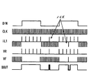
- FIG. 3 is a detailed timing chart showing the operation of the signal transmission circuit.
- FIG. 4 is a schematic timing chart showing the operation of the signal transmission circuit
- FIG. 5 is a diagram showing an electrical configuration of a signal transmission circuit according to the prior art.
- FIG. 6 is a diagram showing a simulation result of each waveform showing the operation of the prior art, FIG.
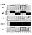
- FIG. 7 is a diagram showing a simulation result of each signal waveform when the pulse period output in the period in which the input signal DIN is at a high level is 0.5 ⁇ sec in the first embodiment.
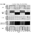
- FIG. 8 is a diagram showing a simulation result of each signal waveform when the pulse period is 1.0 ⁇ sec.
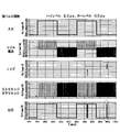
- FIG. 9 is a diagram showing a simulation result of each signal waveform when the pulse period is 2.0 ⁇ sec.
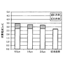
- FIG. 10 is a diagram comparing current consumption between the prior art and the case shown in FIGS.
- FIG. 11 is a diagram showing the electrical configuration of the signal transmission circuit according to the second embodiment.
- FIG. 12 is a detailed timing chart showing the operation of the signal transmission circuit.
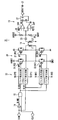
- the inverter circuit 1 is configured by connecting six IGBTs 2U, 2V, 2W, 2X, 2Y, and 2Z (switching elements) with a three-phase bridge.
- a free wheel diode 3 (U to Z) is connected between the collector and emitter of each IGBT 2 (U to Z).
- a smoothing capacitor 5 is connected between the DC buses 4+ and 4- of the inverter circuit 1, and a DC voltage supplied from a DC power source (not shown) is applied.
- Each phase output terminal of the inverter circuit 1 is connected to each phase stator coil (not shown) of the three-phase motor 6.
- a gate signal DOUT (U to Z) is input to the gate of each IGBT 2 (U to Z) via the signal transmission circuit 7 (U to Z).
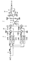
- the signal transmission circuit 7 (drive device) is connected to the transformer 11, the primary circuit 12 connected to the primary coil L1 of the transformer 11, and the secondary coil L2.
- Secondary side circuit 13 In the primary side circuit 12, the input signal DIN is input to one of input terminals of an AND gate 15 (second logic circuit) via a NOT gate 14 (second logic circuit), and another AND gate. It is directly input to one of input terminals 16 (first logic circuit).
- the input signal DIN is a signal that changes to a binary level of high and low at a predetermined frequency. If the high level is “first level”, the low level is “second level”.
- a clock signal CLK (first clock signal) supplied from an oscillation circuit (not shown) is input to the other input terminal of the AND gate 15 and to the other input terminal of the AND gate 16 via the frequency divider 17. Have been entered.
- the frequency of the clock signal CLK is set sufficiently higher (for example, in the order of MHz) than the frequency of the input signal DIN (for example, in the order of kHz).
- the output terminal of the AND gate 15 is connected to each input terminal of the pulse generation circuits 18 (P2) and 19 (N2) (second ON signal output circuit), and the output terminal of the AND gate 16 is connected to the pulse generation circuit 18.
- P1 and 19 (N1) (first on signal output circuit) are connected to the respective input terminals.
- the pulse generation circuit 18 outputs a low level pulse in one shot with the rising edge (change edge) of the input signal as a trigger.
- the pulse generation circuit 19 outputs a high level pulse in one shot with the rising edge of the input signal as a trigger.
- the former low level pulse width is set to be narrower than the latter high level pulse width.
- the H-bridge circuit 20 includes P-channel MOSFETs 21 (P1) and 21 (P2) (switching elements) and N-channel MOSFETs 22 (N1) and 22 (N2) (switching elements). Parasitic diodes are connected between the drains and sources of these FETs 21 and 22. Between the power supply AVDD1 and the ground GND1, a series circuit of FETs 21 (P1) and 22 (N2) and a series circuit of FETs 21 (P2) and 22 (N1) are connected. A common connection point of these series circuits, that is, each output terminal of the H-bridge circuit 20 is connected to both ends of the primary side coil L1 of the transformer 11.
- the secondary side coil L2 of the transformer 11 is in phase with the primary side coil L1.
- One end of the secondary coil L2 is connected to the ground GND2, and the other end is connected to the non-inverting input terminal of the comparator 24R (set signal generation circuit) and the inverting input terminal of the comparator 24F (reset signal generation circuit) via the capacitor 23.
- a series circuit of resistance elements 25 and 26 is connected between the power supply AVDD2 and the ground GND2, and these common connection points are connected to the input terminals of the comparators 24R and 24F.
- the reference voltage REF1 is applied to the inverting input terminal of the comparator 24R, and the reference voltage REF2 is applied to the non-inverting input terminal of the comparator 24F.
- the output terminals of the comparators 24R and 24F are connected to the set terminal S and the reset terminal R of the RS flip-flop 27, respectively.
- the gate signal DOUT is output from the output terminal Q of the RS flip-flop 27.
- the clock signal CLK2 (second clock signal) output via the frequency divider 17 is divided by two.
- the AND gate 16 outputs the clock signal CLK2 as the signal DIN1 during the period when the input signal DIN is at a high level (gate control).
- the AND gate 15 outputs the clock signal CLK as the signal DIN2 during a period in which the input signal DIN is at a low level.
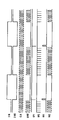
- the pulse generation circuits 18 (P1) and 19 (N1) receive the low-level pulse VP1 and the high-level pulse VN1 (first on signal), respectively, using the rising edge of the signal DIN1 as a trigger during the period in which the input signal DIN shows a high level. Output. Since these pulses become the gate signals of the FETs 21 (P1) and 22 (N1), the primary coil L1 of the transformer 11 has a current in one direction, for example, positive polarity during the period when both are simultaneously turned on. Flowing.
- an in-phase current is induced in the secondary coil L2, and when the potential of the non-inverting input terminal of the comparator 24R exceeds the reference voltage REF1, the comparator 24R generates a pulsed set signal VR and the period of the clock signal CLK2. To output a plurality of times (see FIG. 4). Accordingly, the RF flip-flop 27 is intermittently and continuously set, and the output signal DOUT continues to show a high level during that time.
- the pulse generation circuits 18 (P2) and 19 (N2) are triggered by the rising edge of the signal DIN2 during the period when the input signal DIN is at the low level, respectively, and the low level pulse VP2 and the high level pulse VN2 (second on signal). ) Is output. Since these pulses become the gate signals of the FETs 21 (P2) and 22 (N2), the primary side coil L1 of the transformer 11 has a current in the reverse direction, that is, a negative polarity during the period when both are simultaneously turned on. Flowing.
- an in-phase current is induced in the secondary coil L2, and when the potential of the inverting input terminal of the comparator 24F falls below the reference voltage REF2, the comparator 24F generates a pulsed reset signal VF in the cycle of the clock signal CLK1. Output multiple times (see FIG. 4). As a result, the RF flip-flop 27 is intermittently and continuously reset, and the output signal DOUT continues to show a low level during this period.
- the output signal DOUT becomes a signal in phase with the input signal DIN as shown in FIG. Further, in the figure, the current IL1 flowing through the primary coil L1 is indicated by positive and negative bipolar pulses according to the flowing direction.
- the reset signal VF When negative current is applied when the current IL1 is positive, the reset signal VF is output during the period in which the set signal VR is continuously output, and the RS flip-flop 27 is reset.
- the output signal DOUT is inverted from the high level to indicate the low level. Also in this case, since the set signal VR is continuously output, the RS flip-flop 27 is set immediately thereafter, and the output signal DOUT immediately returns to the high level.
- the IGBT 2 is turned on when the signal applied to the gate is at a high level and turned off when the signal is at a low level. For this reason, the output signal DOUT indicates a low level and the noise is generated when the IGBT 2 is turned off, rather than the event that the output signal DOUT indicates a high level and the IGBT 2 is turned on. It can be evaluated that it is safer to avoid the event of turning on by the application of.
- the reset signal VF is repeatedly output at a cycle faster than that of the set signal VR, so that the reset state can be returned more quickly even if the RS flip-flop 27 is set due to the influence of noise. Moreover, there is an effect of reducing the power consumption of the signal transmission circuit 7 by delaying the cycle on the side of the set signal VR that is less urgent.
- FIG. 5 shows the configuration disclosed in Patent Document 2 at a level corresponding to FIG. 1 of the present embodiment.
- AND gates 15 and 16 are configured by the configuration of the present embodiment without using the clock signal CLK.
- the frequency divider 17 is omitted.
- the output signal DOUT maintains an inverted level until the next formal signal change edge is input. Will continue. Therefore, for example, when the upper arm IGBT 2U is turned off and the lower arm IGBT 2X is turned on and the upper arm IGBT 2U is turned on under the influence of noise, a short-circuit current continues to flow during that time. become. If the state in which the short-circuit current flows continues as it is, the IGBTs 2U and 2X may be destroyed.
- FIGS. 7 to 9 show that the pulse period output during the period when the input signal DIN shows the low level is fixed to 0.5 ⁇ sec, and the pulse period output during the period when the input signal DIN shows the high level is 0.5 ⁇ sec and 1.0 ⁇ sec. , Each signal waveform is simulated when it is changed to 2.0 ⁇ sec.
- the secondary side circuit 13 has the same configuration, so that the secondary side The side current consumption is substantially the same.
- the primary side circuit 12 generates a pulse based on the clock signal CLK, and the current consumption increases accordingly.
- the primary-side current consumption can be reduced by increasing the period of the pulse signal output during the period in which the input signal DIN is at the high level.
- the primary side circuit 12 constituting the signal transmission circuit 7 applies a one-way current to the primary side coil L1 of the transformer 11 during the period in which the input signal DIN is at a high level.
- the pulse signal to be sent is generated at a cycle faster than the change cycle of the input signal.
- a pulse signal for causing a current in the direction opposite to the above direction to flow in the primary coil L1 during a period when the input signal DIN is at a low level is generated at a cycle that is faster than the change cycle of the input signal DIN.
- the secondary side circuit 13 reproduces the input signal by discriminating between the high level and the low level according to the voltages having different polarities generated in the secondary side coil L2 of the transformer 11.
- the secondary side coil L2 has a binary level of the primary side circuit 12.
- a current based on a pulse signal having a faster cycle generated according to the current flows repeatedly, and a voltage having a polarity corresponding to the current is generated.
- the secondary circuit 13 regenerates the input signal DIN according to the polarity of the voltage, so that the inverted level of the input signal DIN is restored to the original level within a short time.
- the input signal DIN is a PWM signal with a duty of 50%, it can be restored to the original level within a time less than 1 ⁇ 2 of the carrier cycle at the latest. Therefore, the transformer 11 is used for electrical insulation between the primary side and the secondary side, the influence of the level inversion is reduced, and the control using the input signal DIN is quickly restored to the original state. It becomes possible to make it.
- the primary side circuit 12 changes the cycle in which the pulse signal is generated between the period in which the input signal DIN is high level and the period in which the input signal DIN is low level.
- the cycle of the pulse signal generated for the high level at which the IGBT 2 is turned on is relatively accelerated, the input signal DIN is immediately restored to the original level, and the cycle of the pulse signal generated for the low level at which the IGBT 2 is turned off is set. Power consumption can be reduced by relatively slowing down.
- the primary side circuit 12 is divided by a frequency divider 17 that divides the clock signal CLK and outputs the clock signal CLK2, an AND gate 16 that outputs the clock signal CLK2 during a period when the input signal DIN is at a high level, and a low level.
- the clock signal CLK2 output via the NOT gate 14 and the AND gate 15 that output the clock signal CLK during the period shown, the H bridge circuit 20 whose output terminals are connected to both ends of the primary coil L1, and the AND gate 16.
- the pulse generators 18 (P1) and 19 (N1) for outputting the pulse signals VP1 and VN1 to the FETs 21 (P1) and 22 (N1) in synchronization with the rising edge of the clock signal CLK output via the AND gate 15 In synchronization with the rising edge of the pulse signal VP2 to the FETs 21 (P2) and 22 (N2). And configured to include a pulse generation circuit 18 (P2) and 19 for outputting beauty VN2 (N2).
- the output period of pulse signal VP1 and VN1 can be changed according to the frequency division ratio set to the frequency divider 17, and IGBT2 in the ON state is affected by noise. In the case of turn-off, it is possible to adjust the speed of time for returning to the on state and the amount of power consumption reduction.
- the secondary side circuit 13 generates a set signal VR when the voltage generated in the secondary coil L2 indicates one polarity, and generates a reset signal VF when the voltage indicates the other polarity.
- the comparator 24F is configured to include an RS flip-flop 27 to which the set signal VR and the reset signal VF are input. With this configuration, the RS flip-flop 27 is set every time the primary circuit 12 generates the pulse signals VP1 and VN1, and the output signal DOUT is set to the high level, and every time the pulse signals VP2 and VN2 are generated. Reset to set the signal to low level. Therefore, the secondary side circuit 13 can be configured easily.
- the IGBT 2 constituting the inverter circuit 1 is driven by the gate signal DOUT output from the signal transmission circuit 7. Therefore, for example, when the IGBT 2U of the upper arm is turned off and the IGBT 2X of the lower arm is turned on and the IGBT 2U is turned on due to the influence of noise, a situation in which a short-circuit current flows through the IGBTs 2U and 2X can be eliminated within a short time. .
- the signal transmission circuit 31 of the second embodiment is obtained by replacing the primary side circuit 12 with a primary side circuit 32. From the configuration of the first embodiment, an AND gate 16 and a frequency divider are provided. 17 is deleted. The input signal DIN is directly input to the pulse generation circuits 18 (P1) and 19 (N1).
- the low-level pulse VP2 and the high-level pulse VN2 that are output during the period when the input signal DIN indicates the low level are the same as those in the first embodiment.
- the pulse generation circuits 18 (P1) and 19 (N1) trigger a low level pulse VP1 and a high level pulse VN1 once with the rising edge of the input signal DIN as a trigger. Output only. Accordingly, when reverse polarity noise is applied within the period, the output signal DOUT does not go high until the next rising edge of the input signal DIN arrives, as in the prior art.
- the power consumption reduction effect of the signal transmission circuit 31 is maximized on the set signal VR side having a low response urgency without providing a recovery effect when noise is applied.
- the signal transmission circuit 31 deletes the AND gate 16 and the frequency divider 17 from the configuration of the first embodiment, and replaces the primary side circuit 12 with the primary side circuit 32.
- the input signal DIN is directly input to the pulse generation circuits 18 (P1) and 19 (N1).
- P1 and N1 the pulse generation circuits 18 and 19 (N1).
- the input signal DIN during the period in which the IGBT 2 is on is not modulated by the primary side circuit 32. If the signal level is inverted due to the influence of noise within that period, the IGBT 2 is turned off and the input signal DIN Does not turn on until the next high level. Therefore, the effect of reducing the power consumption can be improved as compared with the first embodiment, and the same effect as that of the first embodiment can be obtained during the period in which the input signal DIN is at a low level.
- the first and second levels may be either high level and the other low level.
- the falling edge may be a falling edge.
- the division ratio in the frequency divider 17 may be “3” or more.
- the frequency divider 17 may be deleted.
- the switching element for inputting the drive signal via the signal transmission circuit is not limited to the IGBT but may be a MOSFET or a bipolar transistor.
- a drive device may be configured by adding a pre-driver to the signal transmission circuit.
- the switching element driven by the output signal DOUT is not limited to the one constituting the inverter circuit 1 but may be one constituting a half bridge circuit or an H bridge circuit. Further, a single switching element may be a driving target.
- the present invention can be applied to an input signal that needs to be electrically insulated and transmitted at a binary level.
- 1 is an inverter circuit
- 2 is an IGBT (switching element)
- 7 is a signal transmission circuit (drive device)
- 11 is a transformer
- L1 is a primary coil
- L2 is a secondary coil
- 12 is a primary circuit.
- 13 is a secondary circuit
- 14 is a NOT gate (second logic circuit)
- 15 is an AND gate (second logic circuit)
- 16 is an AND gate (first logic circuit)
- 17 is a frequency divider
- 18 (P1 ) And 19 (N1) are pulse generation circuits (first on signal output circuits)
- 18 (P2) and 19 (N2) are pulse generation circuits (second on signal output circuits)
- 20 is an H bridge circuit
- 21 (P1 ) And 21 (P2) are P-channel MOSFETs (switching elements)
- 22 (N1) and 22 (N2) are N-channel MOSFETs (switching elements)
- 24R is a comparator (set signal generating circuit)
- 27 denotes an RS flip-flop.
- the above disclosure includes the following aspects.
- the signal transmission circuit includes a transformer and a pulse signal that causes a unidirectional current to flow through the primary coil of the transformer during a period in which an input signal that changes at a binary level indicates the first level.
- a pulse signal that causes a current in a direction opposite to the direction to flow through the primary coil
- the input signal is determined by determining the first and second levels in accordance with a voltage generated in a primary side circuit generated at a cycle faster than a signal change cycle and a polarity generated in a secondary side coil of the transformer.
- a secondary side circuit for reproducing the signal.
- the primary side circuit is provided in the secondary coil of the transformer.
- a current based on a pulse signal having a faster cycle generated according to the first or second level flows repeatedly, and a voltage having a polarity corresponding to the current is generated.
- the secondary circuit reproduces the input signal according to the polarity of the voltage, the inverted level is restored to the original first or second level within a short time. Therefore, while using a transformer to achieve electrical insulation between the primary and secondary sides, the effect caused by the level inversion due to noise is reduced, and control using the input signal is quickly restored to its original state. It becomes possible to make it.
- the primary side circuit may change the period for generating the pulse signal between a period in which the input signal indicates the first level and a period in which the input signal indicates the second level.
- the on / off control of the switching element is performed using the input signal regenerated by the secondary side circuit.
- the switching element is turned on at one of the binary levels indicated by the input signal and turned off at the other.
- (1) the switching element in the on state is turned off due to the influence of noise is safer than the case in which (2) the switching element in the off state is turned on.
- a short-circuit current may flow in the case (2).
- the period of the pulse signal generated for the level corresponding to the case (2) is made relatively fast so that the input signal can be quickly returned to the original level and generated for the level corresponding to the case (1). Power consumption can be reduced by relatively slowing the period of the pulse signal to be generated.
- the signal transmission circuit causes a current in one direction to flow through the primary coil of the transformer when the transformer and the input signal that changes at the binary level indicate the first level.
- a pulse signal is generated, and a pulse signal that causes a current in a direction opposite to the direction to flow in the primary coil is generated in a period faster than the change period of the input signal during a period in which the input signal indicates the second level.
- a secondary circuit for reproducing the input signal by discriminating between the first and second levels according to voltages having different polarities generated in the secondary coil of the transformer. .
- the switching element is turned on at the first level and the switching element is turned off at the second level.
- the switching element is turned off when the signal level is inverted due to the influence of noise during the period, and the input signal is next. Do not turn on until the first level is shown. If this state is acceptable, the effect of reducing power consumption can be obtained more than the above alternative. The same effect as the above alternative can be obtained for the period in which the signal is at the second level.
- the switching element driving device includes the signal transmission circuit according to the first or second aspect.
- the switching element is driven and controlled by the input signal reproduced by the secondary circuit of the signal transmission circuit.
Landscapes
- Engineering & Computer Science (AREA)
- Power Engineering (AREA)
- Electronic Switches (AREA)
- Power Conversion In General (AREA)
Priority Applications (3)
| Application Number | Priority Date | Filing Date | Title |
|---|---|---|---|
| US15/548,446 US20180019747A1 (en) | 2015-04-15 | 2016-03-25 | Signal transmission circuit and driving device for switching element |
| CN201680017591.0A CN107431483A (zh) | 2015-04-15 | 2016-03-25 | 信号传递电路以及开关元件的驱动装置 |
| DE112016001759.6T DE112016001759T5 (de) | 2015-04-15 | 2016-03-25 | Signalübertragungsschaltung und ansteuervorrichtung für schaltelement |
Applications Claiming Priority (2)
| Application Number | Priority Date | Filing Date | Title |
|---|---|---|---|
| JP2015083318A JP6376029B2 (ja) | 2015-04-15 | 2015-04-15 | 信号伝達回路及びスイッチング素子の駆動装置 |
| JP2015-083318 | 2015-04-15 |
Publications (1)
| Publication Number | Publication Date |
|---|---|
| WO2016166941A1 true WO2016166941A1 (ja) | 2016-10-20 |
Family
ID=57126126
Family Applications (1)
| Application Number | Title | Priority Date | Filing Date |
|---|---|---|---|
| PCT/JP2016/001754 Ceased WO2016166941A1 (ja) | 2015-04-15 | 2016-03-25 | 信号伝達回路及びスイッチング素子の駆動装置 |
Country Status (5)
| Country | Link |
|---|---|
| US (1) | US20180019747A1 (enExample) |
| JP (1) | JP6376029B2 (enExample) |
| CN (1) | CN107431483A (enExample) |
| DE (1) | DE112016001759T5 (enExample) |
| WO (1) | WO2016166941A1 (enExample) |
Families Citing this family (10)
| Publication number | Priority date | Publication date | Assignee | Title |
|---|---|---|---|---|
| GB2559423B8 (en) * | 2017-02-07 | 2023-06-28 | Heyday Integrated Circuits Sas | An isolated high side drive circuit |
| DE102018211033A1 (de) * | 2018-07-04 | 2020-01-09 | Laird Dabendorf Gmbh | Verfahren zum Betrieb einer Schaltung zur Erzeugung eines elektromagnetischen Felds und Schaltung |
| JP7119681B2 (ja) * | 2018-07-16 | 2022-08-17 | 株式会社デンソー | 信号伝達装置及び駆動装置 |
| CN115812279A (zh) * | 2020-10-07 | 2023-03-17 | 罗姆股份有限公司 | 传输电路 |
| US11495172B2 (en) | 2020-10-19 | 2022-11-08 | X Display Company Technology Limited | Pixel group and column token display architectures |
| US11488518B2 (en) | 2020-10-19 | 2022-11-01 | X Display Company Technology Limited | Pixel group and column token display architectures |
| US11430375B1 (en) | 2021-03-19 | 2022-08-30 | X Display Company Technology Limited | Pulse-density-modulation pixel control circuits and devices including them |
| US11386826B1 (en) | 2021-06-22 | 2022-07-12 | X Display Company Technology Limited | Flat-panel pixel arrays with signal regeneration |
| JP7695764B2 (ja) * | 2022-03-18 | 2025-06-19 | 株式会社東芝 | 送受信回路 |
| TWI903681B (zh) * | 2024-08-08 | 2025-11-01 | 友達光電股份有限公司 | 顯示裝置 |
Citations (4)
| Publication number | Priority date | Publication date | Assignee | Title |
|---|---|---|---|---|
| JPH0287963A (ja) * | 1988-09-21 | 1990-03-28 | Nippon Inter Electronics Corp | Mos−fetゲート駆動回路 |
| JPH05252730A (ja) * | 1991-12-09 | 1993-09-28 | Abb Stroemberg Drives Oy | 半導体スイッチ用制御回路 |
| JPH0715949A (ja) * | 1993-06-28 | 1995-01-17 | Fuji Electric Co Ltd | 電力変換装置のゲート駆動回路 |
| JP2001267905A (ja) * | 2000-03-22 | 2001-09-28 | Nippon Koden Corp | 半導体スイッチ駆動回路 |
Family Cites Families (4)
| Publication number | Priority date | Publication date | Assignee | Title |
|---|---|---|---|---|
| JP3522668B2 (ja) * | 2000-08-10 | 2004-04-26 | ローム株式会社 | 信号伝達装置 |
| CN102763387B (zh) * | 2010-02-01 | 2015-07-15 | 丰田自动车株式会社 | 信号传递装置 |
| CN102832917B (zh) * | 2012-08-21 | 2016-03-23 | 台达电子工业股份有限公司 | 开关驱动电路 |
| CN103618437A (zh) * | 2013-11-26 | 2014-03-05 | 苏州贝克微电子有限公司 | 一种使较宽电流范围内的开关稳压电路维持高效率的控制电路 |
-
2015
- 2015-04-15 JP JP2015083318A patent/JP6376029B2/ja not_active Expired - Fee Related
-
2016
- 2016-03-25 DE DE112016001759.6T patent/DE112016001759T5/de not_active Withdrawn
- 2016-03-25 US US15/548,446 patent/US20180019747A1/en not_active Abandoned
- 2016-03-25 CN CN201680017591.0A patent/CN107431483A/zh active Pending
- 2016-03-25 WO PCT/JP2016/001754 patent/WO2016166941A1/ja not_active Ceased
Patent Citations (4)
| Publication number | Priority date | Publication date | Assignee | Title |
|---|---|---|---|---|
| JPH0287963A (ja) * | 1988-09-21 | 1990-03-28 | Nippon Inter Electronics Corp | Mos−fetゲート駆動回路 |
| JPH05252730A (ja) * | 1991-12-09 | 1993-09-28 | Abb Stroemberg Drives Oy | 半導体スイッチ用制御回路 |
| JPH0715949A (ja) * | 1993-06-28 | 1995-01-17 | Fuji Electric Co Ltd | 電力変換装置のゲート駆動回路 |
| JP2001267905A (ja) * | 2000-03-22 | 2001-09-28 | Nippon Koden Corp | 半導体スイッチ駆動回路 |
Also Published As
| Publication number | Publication date |
|---|---|
| DE112016001759T5 (de) | 2018-01-25 |
| CN107431483A (zh) | 2017-12-01 |
| JP6376029B2 (ja) | 2018-08-22 |
| JP2016208078A (ja) | 2016-12-08 |
| US20180019747A1 (en) | 2018-01-18 |
Similar Documents
| Publication | Publication Date | Title |
|---|---|---|
| JP6376029B2 (ja) | 信号伝達回路及びスイッチング素子の駆動装置 | |
| US6664822B2 (en) | Driving device having dummy circuit | |
| JP4640495B2 (ja) | 電気絶縁型スイッチング素子駆動装置 | |
| JP2013013044A (ja) | ゲートドライブ回路 | |
| US20130194006A1 (en) | Dead time generation circuit and load driving apparatus | |
| TW201315150A (zh) | 位準移位電路 | |
| TWI683541B (zh) | 位準移位電路 | |
| US11368111B2 (en) | Method to reduce the commutation loss in a motor inverter | |
| US8994437B2 (en) | Semiconductor device and circuit for controlling potential of gate of insulated gate type switching device | |
| JP7497257B2 (ja) | 電子回路及び電力変換器 | |
| JP6354937B2 (ja) | 駆動回路、集積回路装置及びチャージポンプ回路の制御方法 | |
| US9673735B2 (en) | Power converter | |
| JP2016046775A (ja) | ハイサイドトランジスタのゲート駆動回路、スイッチング出力回路、インバータ装置、電子機器 | |
| JP2004194450A (ja) | 電圧駆動型素子の駆動装置 | |
| CN101483426B (zh) | 输出驱动电路 | |
| US9755628B2 (en) | Driving circuit, converter and driving method | |
| JP5594263B2 (ja) | ハーフブリッジ回路 | |
| CN116633341A (zh) | 驱动装置的电位转换电路 | |
| US7719861B2 (en) | Signal differentiation with differential conversion circuit | |
| JP2022093787A (ja) | モータドライバ装置 | |
| JP6399019B2 (ja) | ゲート電圧制御装置 | |
| JP6277691B2 (ja) | 制御信号生成回路及び回路装置 | |
| Chen | A PMOS-driven H-bridge without dead time for industry applications | |
| WO2024089896A1 (ja) | 電力用半導体素子のゲート駆動装置及び電力変換装置 | |
| JP2018148729A (ja) | 電力変換装置 |
Legal Events
| Date | Code | Title | Description |
|---|---|---|---|
| 121 | Ep: the epo has been informed by wipo that ep was designated in this application |
Ref document number: 16779740 Country of ref document: EP Kind code of ref document: A1 |
|
| WWE | Wipo information: entry into national phase |
Ref document number: 15548446 Country of ref document: US |
|
| WWE | Wipo information: entry into national phase |
Ref document number: 112016001759 Country of ref document: DE |
|
| 122 | Ep: pct application non-entry in european phase |
Ref document number: 16779740 Country of ref document: EP Kind code of ref document: A1 |