WO2016159016A1 - 共振子 - Google Patents
共振子 Download PDFInfo
- Publication number
- WO2016159016A1 WO2016159016A1 PCT/JP2016/060262 JP2016060262W WO2016159016A1 WO 2016159016 A1 WO2016159016 A1 WO 2016159016A1 JP 2016060262 W JP2016060262 W JP 2016060262W WO 2016159016 A1 WO2016159016 A1 WO 2016159016A1
- Authority
- WO
- WIPO (PCT)
- Prior art keywords
- arm
- electrodes
- holding
- unit
- vibration
- Prior art date
- Legal status (The legal status is an assumption and is not a legal conclusion. Google has not performed a legal analysis and makes no representation as to the accuracy of the status listed.)
- Ceased
Links
Images





Classifications
-
- H—ELECTRICITY
- H03—ELECTRONIC CIRCUITRY
- H03H—IMPEDANCE NETWORKS, e.g. RESONANT CIRCUITS; RESONATORS
- H03H9/00—Networks comprising electromechanical or electro-acoustic elements; Electromechanical resonators
- H03H9/15—Constructional features of resonators consisting of piezoelectric or electrostrictive material
- H03H9/17—Constructional features of resonators consisting of piezoelectric or electrostrictive material having a single resonator
- H03H9/19—Constructional features of resonators consisting of piezoelectric or electrostrictive material having a single resonator consisting of quartz
-
- H—ELECTRICITY
- H03—ELECTRONIC CIRCUITRY
- H03H—IMPEDANCE NETWORKS, e.g. RESONANT CIRCUITS; RESONATORS
- H03H9/00—Networks comprising electromechanical or electro-acoustic elements; Electromechanical resonators
- H03H9/15—Constructional features of resonators consisting of piezoelectric or electrostrictive material
- H03H9/205—Constructional features of resonators consisting of piezoelectric or electrostrictive material having multiple resonators
Definitions
- the present invention relates to a resonator.
- a piezoelectric resonance apparatus using a MEMS (Micro Electro Mechanical Systems) technique has been used as a timing device, for example.
- This piezoelectric resonance device is mounted on a printed circuit board incorporated in an electronic device such as a smartphone.
- Patent Document 1 discloses a configuration of a resonator in which upper electrodes are connected to each other by a bus bar, and then the electrodes are drawn from a vibrating portion to an outer peripheral holding portion.
- the conventional resonator described in Patent Document 1 has a problem that the characteristics are deteriorated due to the influence of the parasitic capacitance generated between the end electrode and the upper electrode.
- the upper electrode since it is necessary to provide an end electrode at the end of the vibration part, the upper electrode may not be disposed up to the end of the vibration part.
- the present invention has been made in view of such circumstances, and an object thereof is to provide a resonator capable of reducing the influence of a parasitic capacitance generated between a connection line connecting electrodes and an electrode.
- a resonator has first and second long sides and first and second short sides, and is provided so as to surround a rectangular vibrating portion that vibrates in outline, and around the vibrating portion, A holding part that holds the vibrating part, a first arm provided substantially parallel to the vibrating part between the holding part and the first long side, and a plurality of connecting the first arm and the vibrating part
- the first arm provided on the first arm, the first arm having the second arm, the third arm connecting the first arm and the holding portion, and connecting the vibrating portion and the holding portion.
- first lead lines for connecting the second electrode and the first connection line, wherein the plurality of first lead lines are connected to the first connection line and are connected to the first connection line.
- the first terminal may be provided in the holding portion at a position facing the first long side, or may be routed to a position facing the first short side.
- the resonator includes four or more electrodes, and further includes a first arm provided substantially in parallel along the vibration portion between the holding portion and the second long side, and the first arm and the vibration.
- a second holding unit that has a plurality of second arms that connect the first part and a third arm that connects the first arm and the holding part, and that connects the vibrating part and the holding part;
- a second connection line provided on the first arm, a second terminal provided on the holding portion, and a third and fourth electrode among the four or more electrodes provided on the plurality of second arms.
- a plurality of second lead lines connecting the second connection lines, the plurality of second lead lines are connected to the second connection lines, and the second connection lines are electrically connected to the second terminals.
- an electric field having a phase different from that applied to the first and second electrodes is applied to the third and fourth electrodes.
- the second terminal may be provided at a position facing the second long side in the holding portion, or may be provided at a position facing the second short side.
- a connection line for connecting electrodes to which an electric field having the same phase is applied is provided outside the vibrating portion.
- a certain gap is provided between the connection line and, in particular, an electrode to which an electric field having an opposite phase to the electric field connected to the connection line is applied. Therefore, the influence of parasitic capacitance can be reduced. Therefore, the vibration characteristics of the vibration part can be improved. Furthermore, since it is not necessary to provide a bus bar in the vibration part, it is possible to arrange electrodes up to the end of the vibration part.
- two of the plurality of second arms of the first holding unit are provided corresponding to the first and second electrodes, respectively, and two of the plurality of second arms of the second holding unit. Are preferably provided corresponding to the third and fourth electrodes, respectively.
- the pair of holding units included in the resonator has a configuration that is vertically and horizontally symmetrical. As a result, it is possible to suppress vibration disturbances caused by coupling unnecessary vibration modes to higher-order contour vibrations.
- a resonator includes a pair of first sides facing each other and a pair of second sides facing each other, a rectangular vibrating portion that performs contour vibration, and a vibrating portion
- a holding unit that is provided so as to surround the periphery, and that holds the vibrating unit; a first holding unit having a plurality of arms that connect the vibrating unit and the holding unit between the holding unit and the first side; and a holding unit
- the first connection line provided at a position facing at least one of the pair of first sides, the first terminal provided on the holding unit, and at least 3 provided on the vibration unit.
- One or more electrodes and a plurality of first lead lines provided on the plurality of arms of the first holding unit and connecting the first and second electrodes of the three or more electrodes and the first connection line.
- the plurality of first lead wires are connected to the first connection line, and the first connection line is electrically connected to the first terminal. Is connected to the first and second electrodes, the electric field of the same phase are applied from the first terminal.
- the first terminal may be provided in the holding portion at a position facing the first long side, or may be routed to a position facing the first short side.
- the resonator includes four or more electrodes, and further includes a plurality of arms that connect the vibrating unit and the holding unit between the holding unit and the other side of the pair of first sides.
- the second connection line is electrically connected to the second terminal, and the third and fourth electrodes are preferably applied with an electric field having a phase different from that applied to the first and second electrodes.
- the second terminal may be provided at a position facing the second long side in the holding portion, or may be provided at a position facing the second short side.
- the holding unit can be shortened by providing the connection line on the holding portion. Therefore, even if the width of the holding unit is reduced in order to reduce the loss of vibration, the resonance resistance of the holding unit can be reduced.
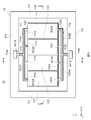
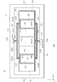
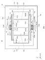
- FIG. 1 is an exploded perspective view schematically showing a structure of a resonance device according to a first embodiment. It is a top view which shows roughly an example of the structure of the resonator which concerns on 1st Embodiment. It is a figure which shows roughly an example of the structure of the cross section of the resonator which concerns on 1st Embodiment. It is a top view which shows roughly an example of the structure of the resonator which concerns on 2nd Embodiment. It is a top view which shows roughly an example of the structure of the resonator which concerns on 3rd Embodiment.
- FIG. 1 is a perspective view schematically showing the appearance of the resonance device 1 according to the first embodiment of the present invention.
- the resonance device 1 includes a lower substrate 14, an upper substrate 13 that forms a vibration space between the lower substrate 14, and a resonator 10 that is sandwiched and held between the lower substrate 14 and the upper substrate 13.
- the resonator 10 is a MEMS vibrator manufactured using the MEMS technology.
- FIG. 2 is an exploded perspective view schematically showing the structure of the resonance device 1 according to the first embodiment of the present invention.
- the lower substrate 14 extends in a flat plate shape along the XY plane, and a flat rectangular parallelepiped concave portion 17 is formed on the upper surface thereof.
- the recess 17 forms a part of the vibration space of the resonator 10.
- the upper substrate 13 extends in a flat plate shape along the XY plane, and a flat rectangular parallelepiped concave portion 18 is formed on the lower surface thereof.
- the recess 18 forms part of the vibration space of the resonator 10. A vacuum state is maintained in this vibration space.
- the lower substrate 14 and the upper substrate 13 are made of, for example, Si (silicon).
- FIG. 3 is a plan view schematically showing the structure of the resonator 10 according to the present embodiment.
- the resonator 10 includes a vibrating unit 120, a holding unit 11, a holding unit 111 (an example of a first holding unit), 112 (an example of a second holding unit), and a connection line B121 (first first).
- B122 an example of a second connection line
- lead lines W111 and W121 an example of a first lead line
- W123 an example of a first lead line
- W112, W122 an example of a second lead line
- W124 an example of a second lead line.
- the vibrating unit 120 has a substantially rectangular parallelepiped outline extending in a flat plate shape along the XY plane in the orthogonal coordinate system of FIG.
- the vibration unit 120 On the vibration unit 120, four rectangular plate-shaped upper electrodes 121 to 124 (an example of the first electrode to the fourth electrode) having a length direction and a width direction are provided.
- the vibration unit 120 has a long side in the X-axis direction and a short side in the Y-axis direction, and the four upper electrodes 121 to 124 all have long sides in the Y-axis direction and short sides in the X-axis direction. have.
- a space is formed between the vibrating unit 120 and the holding unit 11 at a predetermined interval.
- the vibration unit 120 is connected to and held by the holding unit 11 by holding units 111 and 112 described later on a pair of long sides, respectively.
- the vibration unit 120 is not held by the holding unit 11 on a pair of short sides.
- FIG. 4A is a cross-sectional view taken along the line AA ′ of FIG.
- a lower electrode 129 is stacked on a Si substrate 130 made of a degenerate semiconductor.
- the Si substrate 130 is desirably about 140 ⁇ m long, about 400 ⁇ m wide, and about 10 ⁇ m thick.
- the lower electrode 129 is formed using, for example, a metal such as molybdenum (Mo) or aluminum (Al), and has a thickness of about 0.1 ⁇ m. Note that the Si substrate 130 which is a degenerated semiconductor may be used as the lower electrode without forming the lower electrode 129.
- a piezoelectric thin film 128 is laminated on the lower electrode 129 so as to cover the lower electrode 129, and further, upper electrodes 121 to 124 are laminated on the piezoelectric thin film 128. After the upper electrodes 121 to 124 are formed on the vibration unit 120, the upper electrodes 121 to 124 are divided into four by processing such as etching.
- the piezoelectric thin film 128 is a piezoelectric thin film that converts an applied voltage into vibration.
- the piezoelectric thin film 128 can be mainly composed of a nitride such as aluminum nitride or an oxide.
- the piezoelectric thin film 128 can be formed of scandium aluminum nitride (ScAlN).
- ScALN is obtained by replacing a part of aluminum (Al) in aluminum nitride (AlN) with scandium (Sc).
- the piezoelectric thin film 128 has a thickness of 0.8 ⁇ m, for example.
- the upper electrodes 121 to 124 are formed using a metal such as molybdenum (Mo) or aluminum (Al), and have a thickness of about 0.1 ⁇ m.
- the vibration unit 120 undergoes contour vibration along the X-axis direction when an alternating electric field is applied.
- the piezoelectric thin film 128 is oriented in the c-axis direction, so that a predetermined electric field is applied to the upper electrodes 121 to 124 and a predetermined potential difference is generated between the lower electrode 129 and the upper electrodes 121 to 124. Is formed, the piezoelectric thin film 128 expands and contracts in the XY in-plane direction in accordance with the potential difference, so that the vibration unit 120 undergoes contour vibration.
- the vibration unit 120 is divided into vibration regions A121 to A124 corresponding to the upper electrodes 121 to 124. That is, upper electrodes 121 to 124 are formed in the vibration regions A121 to A124, respectively.
- the adjacent vibration regions A121 to 124 are mechanically coupled.
- the vicinity of the center in the X-axis direction of each region becomes a vibration node, and the four vibration regions A121 to A124 vibrate in the in-plane direction with the adjacent regions having opposite phases.
- the vibration unit 120 vibrates at a higher order as a whole.
- the Si substrate 130, the lower electrode 129, and the piezoelectric thin film 128 are shared by the vibration regions A121 to A124.
- the holding unit 11 is formed in a rectangular frame shape along the XY plane.
- maintenance part 11 should just be provided in at least one part of the circumference
- the holding unit 11 is provided so as to surround the vibration unit 120 and the outside of the vibration unit 120 along the XY plane. More specifically, the holding unit 11 includes a pair of long-side plate-like frames 11 a and 11 b extending in parallel with the X-axis direction so as to face the long side of the vibration unit 120, and the short side of the vibration unit 120. And a pair of short-side frames 11c and 11d that extend in parallel to the Y-axis direction and are connected to both ends of the frames 11a and 11b at both ends thereof, respectively.
- the frame body 11a and the frame body 11b are formed with voltage application portions 110a (an example of a first terminal) and 110b (an example of a second terminal).
- the voltage application units 110 a and 110 b can apply an alternating electric field to the upper electrodes 121 to 124 via the holding units 111 and 112.
- the voltage application unit 110a is formed near the center of the frame 11a
- the voltage application unit 110b is formed near the center of the frame 11b.
- the voltage application unit 110a may be formed at 11c and 11d.
- the frame 11a side is described as the upper side of the resonator 10
- the frame 11b side is described as the lower side of the resonator 10.
- a metal layer Z129 formed integrally with the lower electrode 129 of the vibrating unit 120 is formed on the Si substrate 130 made of a degenerate semiconductor.
- a piezoelectric thin film 128 is laminated so as to cover the layer Z129.
- the holding unit 11 is formed integrally with the vibrating unit 120 in this order on the Si substrate 130 in the order of the metal layer Z129 and the piezoelectric thin film 128, and is removed and formed into a desired shape by processing such as etching.
- the metal layer Z129 provided on the holding unit 11 may be removed when the lower electrode 129 is formed into a predetermined shape by etching or the like.
- the holding unit 111 connects the vibrating unit 120 and the holding unit 11.
- the holding unit 111 is provided inside the holding unit 11 along the XY plane and between the long side of the vibrating unit 120 and the frame 11a.
- the holding unit 111 includes a main arm 111n (an example of the third arm of the first holding unit), a support arm 111m (an example of the first arm of the first holding unit), and child arms 111a to 111d. (An example of a plurality of second arms of the first holding unit).
- the support arm 111m is provided in the space between the vibration unit 120 and the frame 11a so as to face the long side of the vibration unit 120 across the upper electrodes 121 to 124 in parallel with the X-axis direction.
- the main arm 111n is provided in parallel to the Y-axis direction so as to face the long side of the vibration unit 120, and connects the support arm 111m and the frame 11a.
- the child arms 111a to 111d are provided in the space between the vibration unit 120 and the frame body 11a so as to face the long side of the vibration unit 120 in parallel with the Y-axis direction.
- the lower arm 111a has a lower end connected to the long side of the vibrating portion 120 near the center of the upper short side of the upper electrode 121, and an upper end connected to one end of the support arm 111m.
- the child arm 111d has a lower end connected to the long side of the vibrating portion 120 near the center of the upper short side of the upper electrode 124, and an upper end connected to the other end of the support arm 111m.
- the lower arm 111b has a lower end connected to the long side of the vibrating portion 120 near the center of the upper short side of the upper electrode 122, and an upper end connected to the support arm 111m.
- the lower arm 111c has a lower end connected to the long side of the vibrating portion 120 near the center of the upper short side of the upper electrode 123, and an upper end connected to the support arm 111m.
- the support arm 111m, the main arm 111n, and the child arms 111a to 111d are all rectangular plates having a long side with a width of about 5 ⁇ m.
- the holding unit 111 has the same number of child arms as the number of electrodes of the vibration unit 120, and is configured to be symmetrical with respect to the main arm 111n in the X-axis direction. As a result, it is possible to suppress vibration disturbances caused by coupling unnecessary vibration modes to higher-order contour vibrations.
- the holding unit 112 connects the vibration unit 120 and the holding unit 11.
- the holding unit 112 is provided between the long side of the vibration unit 120 and the frame body 11b.
- the holding unit 112 includes a main arm 112n (an example of the third arm of the second holding unit), a support arm 112m (an example of the first arm of the second holding unit), and child arms 112a to 112d. (It is an example of a plurality of second arms of the second holding unit).
- the support arm 112m is provided in the space between the vibration unit 120 and the frame 11b so as to face the long side of the vibration unit 120 across the upper electrodes 121 to 124 in parallel with the X-axis direction.
- the main arm 112n is provided in parallel to the Y-axis direction so as to face the short side of the vibration unit 120, and connects the support arm 112m and the frame 11b.
- the child arms 112a to 112d are provided in the space between the vibration unit 120 and the frame 11b so as to face the long side of the vibration unit 120 in parallel with the Y-axis direction.
- the upper end of the child arm 112a is connected to the longer side of the vibrating portion 120 near the center of the lower side of the upper electrode 121, and the lower end is connected to one end of the support arm 112m.
- the child arm 112d has an upper end connected to the long side of the vibrating portion 120 near the center of the lower side of the upper electrode 124, and a lower end connected to the other end of the support arm 112m.
- the upper end of the child arm 112b is connected to the longer side of the vibration unit 120 near the center of the lower side of the upper electrode 122, and the lower end is connected to the support arm 112m.
- the upper end of the child arm 112c is connected to the longer side of the vibration unit 120 near the center of the lower side of the upper electrode 123, and the lower end is connected to the support arm 112m.
- the support arm 112m, the main arm 112n, and the child arms 112a to 112d are all rectangular plates having a long side with a width of about 5 ⁇ m.
- the holding unit 112 has the same number of child arms as the number of electrodes of the vibration unit 120, and is configured to be bilaterally symmetric about the main arm 112n in the X-axis direction. As a result, it is possible to suppress vibration disturbances caused by coupling unnecessary vibration modes to higher-order contour vibrations. Furthermore, the holding unit 111 and the holding unit 112 described above have a symmetrical configuration. Thereby, vibration inhibition can be further suppressed.
- FIG. 4B is a cross-sectional view taken along the line BB ′ in FIG.
- the holding units 111 and 112 are formed by stacking a metal layer Z129 on a Si substrate 130 made of a degenerate semiconductor, and piezoelectrically covering the metal layer Z129 on the metal layer Z129.
- a thin film 128 is laminated.
- connection lines B121 and B122 and lead lines W111, W121, W123, W112, W122, and W124, which will be described later, are integrally formed on the piezoelectric thin film 128 by the same process as the upper electrodes 121 to 124 of the vibration unit 120. Are stacked.
- the Si substrate 130, the metal layer Z129, the piezoelectric thin film 128, the connection lines B121 and B122, and the lead lines W111, W121, W123, W112, W122, and W124 of the holding units 111 and 112 are integrally formed with the vibration unit 120, and are etched. It is removed and formed so as to have a desired shape by processing. Note that the metal layer Z129 provided in the holding units 111 and 112 may be removed when the lower electrode 129 is formed into a predetermined shape by etching or the like.
- connection line B121 is provided in a space between the long side of the vibration unit 120 and the frame 11a.
- the connection line B121 is provided on the surface of the support arm 111m, and extends in parallel with the X-axis direction across the upper electrodes 121 to 124 so as to face the long side of the vibration unit 120.
- the connection line B121 connects the upper electrodes 121 and 123 having the same phase of the electric field extended by the lead lines W121 and W123 among the four upper electrodes 121 to 124 provided on the vibration unit 120.
- the resonator 10 has a configuration in which the connection line B121 connecting the upper electrodes 121 and 123 having the same phase provided in the vibration unit 120 is provided outside the vibration unit 120. . Therefore, since a gap is formed between the connection line B121 and the upper electrode 122, the influence of parasitic capacitance can be reduced. In addition, since it is not necessary to provide a bus bar on the vibration unit 120, the upper electrode 122 can be provided to the end of the vibration unit 120. Furthermore, since the connection line B121 is provided on the holding unit 111, the number of main arms that are connection points between the holding unit 111 and the holding unit 11 can be reduced, and the vibration attenuation of the vibrating unit 120 can be reduced. it can.
- the lead lines W111, W121, W123 are provided in the space between the long side of the vibration unit 120 and the frame body 11a in parallel to the Y-axis direction.
- the lead wire W121 is provided on the surface of the child arm 111a, and the upper electrode 121 extends on the child arm 111a and is connected to the connection line B121.
- the lead wire W123 is provided on the surface of the child arm 111c, and the upper electrode 123 to which an electric field having the same phase as the electric field of the upper electrode 121 is extended on the child arm 111c and connected to the connection line B121.
- the lead line W111 is provided on the main arm 111n, and connects the voltage application unit 110a and the connection line B121.
- connection line B122 is provided in a space between the long side of the vibration unit 120 and the frame body 11b.
- the connecting line B122 is provided on the surface of the support arm 112m, and extends along the upper electrodes 121 to 124 so as to face the long side of the vibrating unit 120 in parallel with the X-axis direction.
- the connection line B122 connects the upper electrodes 122 and 124 having the same phase extended by the lead lines W122 and W124 among the four upper electrodes 121 to 124 provided on the vibration unit 120.
- the resonator 10 has a configuration in which the connection line B122 that connects the upper electrodes of the same phase provided in the vibration unit 120 is provided outside the vibration unit 120.
- connection line B122 since a gap is formed between the connection line B122 and the upper electrode 123, the influence of parasitic capacitance can be reduced.
- the upper electrode 123 can be provided up to the end of the vibration unit 120.
- the connection line B122 is provided on the holding unit 112, the number of main arms that are connection points between the holding unit 112 and the holding unit 11 can be reduced, and the vibration of the vibrating unit 120 can be attenuated. Can be reduced.
- Lead lines W112, W122, W124 Lead lines W112, W122, and W124 are provided in the space between the long side of the vibration unit 120 and the frame 11b in a direction parallel to the Y-axis direction.
- the lead lines W122 are provided on the surface of the child arm 112b.
- An upper electrode 122 is provided on the child arm 112b and connected to the connection line B122.
- the lead line W124 is provided on the surface of the child arm 112d, and the upper electrode 124 to which an electric field having the same phase as the upper electrode 122 is applied extends to the child arm 112d and is connected to the connection line B122.
- the lead line W112 is provided on the surface of the main arm 112n, and connects the voltage application unit 110b and the connection line B122.
- FIG. 5 is a plan view schematically showing an example of the structure of the resonator 10 according to the present embodiment.
- the detailed configuration of the resonator 10 according to the present embodiment will be described focusing on the differences from the first embodiment.
- the vibration unit 120 includes three upper electrodes 121 to 123. Other configurations of the vibration unit 120 are the same as those in the first embodiment.
- the voltage application units 110a and 110b are provided at the ends of the frames 11a and 11b, respectively.
- maintenance part 11 is the same as that of 1st Embodiment.
- the holding unit 111 has only three arms 111b to 111c, and does not have a configuration corresponding to the support arm 111m and the main arm 111n. Other configurations of the holding unit 111 are the same as those in the first embodiment.
- the holding unit 112 has only three arms 112b to 112c, and does not have a configuration corresponding to the support arm 112m and the main arm 112n. Other configurations of the holding unit 112 are the same as those in the first embodiment.
- connection line B121 is provided on the frame 11a so as to face the long side of the vibration unit 120 and in parallel with the X-axis direction.
- the connection line B121 connects the upper electrodes 121 and 123 extended by the lead lines W121 and W123, and is connected to the voltage application unit 110a provided at the end of the frame 11a.
- the resonator 10 according to this embodiment can shorten the holding unit 111 by providing the connection line B121 on the frame 11a. Therefore, the resonance resistance of the holding unit 111 can be reduced even when the width of the holding unit 111 is narrowed in order to reduce vibration loss.
- the configuration of the other connection line B121 is the same as that of the first embodiment.
- the resonator 10 does not have the lead wire W111.
- the configuration of the lead lines W121 and W123 is the same as that of the first embodiment.
- connection line B122 In the present embodiment, the resonator 10 does not have the connection line B122.
- the resonator 10 does not have the lead wire W124.
- the lead wire W112 is provided on the frame 11b so as to face the long side of the vibration unit 120 in parallel with the X-axis direction.
- the lead line W112 connects the upper electrode 122 extended by the lead line W122 to the voltage application unit 110b.
- the configuration of the lead line W122 is the same as that of the first embodiment.
- FIG. 6 is a plan view schematically showing an example of the structure of the resonator 10 according to the present embodiment. Below, the difference with 1st Embodiment is demonstrated among each structure of the resonator 10 which concerns on this embodiment.
- Vibration unit 120 The configuration of the vibration unit 120 is the same as that of the first embodiment.
- the voltage application units 110a and 110b are provided at the ends of the frames 11a and 11b, respectively.
- maintenance part 11 is the same as that of 1st Embodiment.
- the holding unit 111 has only two arms, child arms 111a and 111b, and the number of electrodes provided on the vibration unit 120 does not match the number of child arms. .
- the holding unit 111 does not have a configuration corresponding to the support arm 111m and the main arm 111n.
- the holding unit 111 has a smaller number of child arms than the number of electrodes provided on the vibration unit 120. As a result, the loss of vibration energy leaking from the arm can be reduced as the number of child arms connected to the vibration unit 120 is small, and vibration characteristics are improved.
- the effect of reducing the energy loss can be further improved by using the structure in which the child arm outside the long side of the vibration unit 120 among the child arms of the holding unit 111 is blown.
- Other configurations of the holding unit 111 are the same as those in the first embodiment.
- the holding unit 112 has only two arms, child arms 112a and 112b, and the number of electrodes provided on the vibrating unit 120 does not match the number of child arms. .
- the holding unit 112 does not have a configuration corresponding to the support arm 112m and the main arm 112n.
- the holding unit 112 has a smaller number of child arms than the number of electrodes provided on the vibration unit 120.
- the loss of vibration energy leaking from the arm can be reduced as the number of child arms connected to the vibration unit 120 is small, and vibration characteristics are improved.
- the effect of reducing the energy loss can be further improved by making the child arm outside the long side of the vibration unit 120 out of the child arms of the holding unit 112.
- Other configurations of the holding unit 112 are the same as those in the first embodiment.
- connection line B121 is provided on the frame 11a in a direction parallel to the X-axis direction so as to face the long side of the vibration unit 120.
- the connection line B121 connects the upper electrodes 121 and 123 extended by the lead lines W121 and W123, and is connected to the voltage application unit 110a provided at the end of the frame 11a.
- the configuration of the other connection line B121 is the same as that of the first embodiment.
- the resonator 10 does not have the lead wire W111.
- the configuration of the lead lines W121 and W123 is the same as that of the first embodiment.
- connection line B122 is provided on the frame body 11b in a direction parallel to the X-axis direction so as to face the long side of the vibration unit 120.
- the connection line B122 connects the upper electrodes 122 and 124 extended by the lead lines W122 and W124, and is connected to the voltage application unit 110b provided at the end of the frame 11b.
- the configuration of the other connection line B122 is the same as that of the first embodiment.
- the resonator 10 does not have the lead wire W112.
- the configuration of the lead lines W122 and W124 is the same as that of the first embodiment.
- FIG. 7 is a plan view schematically showing an example of the structure of the resonator 10 according to the present embodiment. Below, the difference with 1st Embodiment is demonstrated among each structure of the resonator 10 which concerns on this embodiment.
- the vibration unit 120 includes seven upper electrodes 121 to 127, a bus bar b121, and a bus bar b125.
- the bus bar b121 is an upper end portion of the vibration unit 120, is provided on the upper electrode 122, and extends along the X-axis direction in parallel with the long side of the vibration unit 120.
- the bus bar b ⁇ b> 125 is provided on the upper end of the upper electrode 126 on the upper end of the vibration unit 120, and extends along the X-axis direction in parallel with the long side of the vibration unit 120.
- the vibration unit 120 includes the bus bars b121 and b125.
- the connection points between the vibration unit 120 and the holding unit 111 can be reduced, and loss of vibration energy of the vibration unit 120 can be reduced.
- the vibration unit 120 by not providing a bus bar on the vibration part 120 at the center of the vibration part 120, it is possible to reduce the parasitic capacitance and to arrange the upper electrode up to the end, and the capacity is large and the resonance resistance is small. Vibration can be obtained.
- Other configurations of the vibration unit 120 are the same as those in the first embodiment.
- the holding unit 111 has child arms 111a, 111b, and 111c, a support arm 111m, and a main arm 111n.
- the number of child arms of the holding unit 111 does not match the number of electrodes provided on the vibration unit 120.
- the holding unit 111 according to this embodiment does not have a child arm connected to the vibration region at the extreme end of the vibration unit 120 or in the vicinity thereof. That is, the holding unit 111 has only a child arm connected to the vibration region at the center of the vibration unit 120 or in the vicinity thereof. Thereby, loss of vibration energy can be reduced.
- Other configurations of the holding unit 111 are the same as those in the first embodiment.
- the holding unit 112 includes child arms 112a, 112b, and 112c, a support arm 112m, and a main arm 112n.
- the number of child arms of the holding unit 112 does not match the number of electrodes provided on the vibration unit 120.
- the holding unit 112 according to the present embodiment does not have the child arm connected to the vibration region at the extreme end of the vibration unit 120 or in the vicinity thereof. That is, the holding unit 112 has only a child arm connected to the vibration region at the center of the vibration unit 120 or in the vicinity thereof. Thereby, loss of vibration energy can be reduced.
- Other configurations of the holding unit 111 are the same as those in the first embodiment.
- connection line B121 The configuration of the connection line B121 of this embodiment is the same as that of the first embodiment.
- the lead lines W121 and W125 are each provided between the long side of the vibration unit 120 and the frame body 11a in a direction parallel to the Y-axis direction.
- the lead line W121 is provided on the child arm 111a, and connects the bus bar b121 that connects the upper electrodes 121 and 123 having the same phase to the connection line B121.
- the lead line W125 is provided on the child arm 111c, and connects the bus bar b125 that connects the upper electrodes 125 and 127 having the same phase to the connection line B121.
- the configuration of the lead line W111 is the same as that of the first embodiment.
- connection line B122 The configuration of the connection line B122 of this embodiment is the same as that of the first embodiment.
- the lead lines W122, W124, and W126 are respectively provided in the direction parallel to the Y-axis direction between the long side of the vibration unit 120 and the frame body 11b.
- the lead-out line W122 is provided on the child arm 112a, extends the upper electrodes 122 having the same phase, and connects to the connection line B122.
- the lead line W124 is provided on the child arm 111b, and extends from the upper electrode 124 to be connected to the connection line B122.
- the lead line W126 is provided on the child arm 112c, and extends from the upper electrode 126 to be connected to the connection line B122.
- the configuration of the lead line W112 is the same as that of the first embodiment.
- FIG. 8 is a plan view schematically showing an example of the structure of the resonator 10 according to the present embodiment. Below, the difference with 1st Embodiment is demonstrated among each structure of the resonator 10 which concerns on this embodiment.
- Vibration unit 120 The configuration of the vibration unit 120 is the same as that of the first embodiment.
- the main arms 111n and 112n of the holding units 111 and 112 have vibration buffer portions 4 that protrude in directions orthogonal to the main arms 111n and 112n, respectively.
- the vibration buffer portion 4 is formed of two pairs of arms 41 and 42 that face each other.
- the arm 41 extends in a direction substantially parallel to the long side of the vibration unit 120.
- the arm 42 is provided in a direction substantially perpendicular to the arm 41 and is connected to both ends of the arm 41 at both ends thereof.
- the main arms 111n and 112n in the holding units 111 and 112 have the vibration buffering portion 4, propagation of vibration to the holding portion 11 can be suppressed, and the contour vibration propagated from the vibrating portion 120 can be suppressed. Harmonic vibrations can be confined efficiently.
- the configuration of the other holding units 111 and 112 is the same as that of the first embodiment.
- connection line B121 The configuration of the connection line B121 of this embodiment is the same as that of the first embodiment.
- the lead wire W111 is formed along the two pairs of arms 41 and 42 so as to cover the surface of the vibration buffer portion 4 in the main arm 111n.
- the lead-out line W111 extends substantially perpendicular to the connection line B121 from the connection point with the connection line B121, and branches bifurcated at the connection point between the arm 41 and the support arm 111m on the vibration buffer portion 4. Then, it extends along the arm 41.
- the bifurcated lead line W111 is bent in a direction substantially perpendicular to the arm 41 and extends along the arm 42 at the connecting portion (supporting arm 111m side) between the arm 41 and the arm 42, and the arm 42 and the arm 41 are further extended.
- the lead line W111 joined into one line extends in a direction substantially perpendicular to the arm 41 from the joining point, and is connected to the voltage application unit 110a.
- the configuration of the lead lines W121 and 125 is the same as that of the first embodiment.
- connection line B122 (6. Connection line B122)
- the configuration of the connection line B122 of this embodiment is the same as that of the first embodiment.
- the lead wire W112 is formed along the two pairs of arms 41 and 42 so as to cover the surface of the vibration buffer portion 4 in the main arm 111n.
- the lead-out line W112 extends substantially perpendicular to the connection line B122 from the connection point with the connection line B122, and bifurcates at the connection point between the arm 41 and the support arm 112m on the vibration buffer 4. Then, it extends along the arm 41.
- the bifurcated lead line W112 bends in a direction substantially perpendicular to the arm 41 and extends along the arm 42 at the connection portion (supporting arm 112m side) between the arm 41 and the arm 42, and further, the arm 42 and the arm 41 Is bent again in a direction substantially perpendicular to the arm 42, extends along the arm 41, and merges into one. Furthermore, the lead wire W112 joined to one line extends in a direction substantially perpendicular to the arm 41 from the joining point, and is connected to the voltage application unit 110b.
- the configuration of the lead lines W122 and 124 is the same as that of the first embodiment.
- FIG. 9 is a plan view schematically showing an example of the structure of the resonator 10 according to the present embodiment. Below, the difference with 1st Embodiment is demonstrated among each structure of the resonator 10 which concerns on this embodiment.
- Vibration unit 120 The configuration of the vibration unit 120 is the same as that of the first embodiment.
- the holding unit 111 includes a connection arm 111f, a holding arm 111g, and a node generation unit 130A instead of the main arm 111n.
- the node generation unit 130 ⁇ / b> A is provided in a region between the long side in the vibration unit 120 and the frame 11 a in the holding unit 11.
- the node generation unit 130A has a side 131a opposite to the long side of the support arm 111m, and the side 131a is connected to the connection arm 111f.
- the side 131a is provided substantially parallel to the long side of the support arm 111m at regular intervals.
- the node generation unit 130A is connected to the support arm 111m by the connection arm 111f, and is connected to the holding unit 11 by the holding arm 111g.
- the node generation unit 130A has a shape whose width along the X-axis direction becomes narrower as it goes from the connecting arm 111f to the holding arm 111g.
- the node generation unit 130A has a line-symmetric shape with respect to the vertical bisector of the side 131a.
- the node generation unit 130A has a portion having a maximum width along the X-axis direction on the connection arm 111f side from the center in the Y-axis direction.
- the width along the X-axis direction of the node generation unit 130A is the maximum at the side 131a, and gradually becomes narrower from the connecting arm 111f toward the holding arm 111g, and the vertex of the node generation unit 130A.
- the holding arm 111g are narrowest at the connection point.
- the width along the X-axis direction of the node generation unit 130A does not need to be continuously reduced.
- the width gradually decreases as a whole even if the width is gradually reduced or partially expanded. It only has to be narrowed.
- the periphery of the node generation unit 130A is not limited to a smooth shape, and may have irregularities.
- the node generation unit 130A has a semicircular shape having a radius of about 30 ⁇ m with the side 131a as a diameter.
- the center of the circle forming the arc of the node generation unit 130A is located at the center of the side 131a.
- the center of the circle forming the arc of the node generation unit 130A may be located at the center of the support arm 111m.
- the side 131a is not limited to a linear shape, and may be an arc shape.
- the connecting arm 111f is connected to the apex of the side 131a.
- the center of the circle forming the arc of the side 131a may be located on the connection arm 111f side or may be located on the holding arm 111g side.
- the length of the side 131a is preferably larger than the width of the connecting arm 111f along the X-axis direction and smaller than the long side of the vibration unit 120.
- the connecting arm 111f has a substantially rectangular shape in the present embodiment.
- One end of the connection arm 111f is connected to the vicinity of the center of the long side of the support arm 111m, and extends substantially perpendicularly to the long side of the support arm 111m from there toward the node generation unit 130A.
- the other end of the connection arm 111f is connected to the side 131a of the node generation unit 130A.
- the width of the connecting arm 111f along the X-axis direction is about 10 ⁇ m.
- the holding arm 111g has a substantially rectangular shape. One end of the holding arm 111g is connected to a portion where the width along the X-axis direction in the node generation unit 130A is the narrowest. The other end of the holding arm 111g is connected to a region of the holding unit 11 that faces the node generation unit 130A.
- the width of the holding arm 111g along the X-axis direction is preferably equal to or smaller than the width of the connection arm 111f. By making the width of the holding arm 111g smaller than the width of the connection arm 111f, it is possible to suppress the propagation of vibration from the node generation unit 130A to the holding unit 11.
- the width of the holding arm 111g along the X-axis direction is smaller than the width of the connection arm 111f and is about 5 ⁇ m.
- the node generation unit 130A of the holding unit 111 in the present embodiment has a structure in which the width along the X-axis direction is gradually narrowed from the connecting arm 111f toward the holding arm 111g. For this reason, even when the propagation state of the vibration propagated from the vibration unit 120 is changed, the node generation unit 130A is formed with a portion having a small displacement adjacent to a portion having a large displacement due to the vibration. Thereby, the node generation unit 130A can adjust the displacement part with respect to the vibration leaked from the vibration unit 120, and can form a vibration node on the node generation unit 130A.
- the node generation unit 130 ⁇ / b> A can suppress the propagation of vibration from the vibration unit 120 to the holding unit 11 by being connected to the holding arm 111 g in the formed node. As a result, the anchor loss of the resonator 10 can be reduced and the Q value can be improved.
- Other configurations of the holding unit 111 are the same as those in the first embodiment.
- the holding unit 112 includes a connection arm 112f, a holding arm 112g, and a node generation unit 130B instead of the main arm 112n.
- the configuration / function of the connection arm 112f is the same as the configuration / function of the connection arm 111f
- the configuration / function of the holding arm 112g is the same as the configuration / function of the holding arm 111g
- the configuration / function of the node generation unit 130B The function is the same as that of the node generation unit 130A.
- connection line B121 The configuration of the connection line B121 of this embodiment is the same as that of the first embodiment.
- the lead line W111 is connected to the vicinity of the center of the connection line B121, and is formed from the connection arm 111f to the holding arm 111g along the vertical bisector of the side 131a of the node generation unit 130A. Is done.
- the configuration of the lead lines W121 and 123 is the same as that in the first embodiment.
- connection line B122 (6. Connection line B122)
- the configuration of the connection line B122 of this embodiment is the same as that of the first embodiment.
- the lead line W112 is connected to the vicinity of the center of the connection line B122 and is formed from the connection arm 112f to the holding arm 112g along the vertical bisector of the side 131b of the node generation unit 130B. Is done.
- the configuration of the lead lines W122 and 124 is the same as that of the first embodiment.
- each embodiment described above is for facilitating the understanding of the present invention, and is not intended to limit the present invention.
- the present invention can be changed / improved without departing from the spirit thereof, and the present invention includes equivalents thereof.
- those obtained by appropriately modifying the design of each embodiment by those skilled in the art are also included in the scope of the present invention as long as they include the features of the present invention.
- each element included in each embodiment and its arrangement, material, condition, shape, size, and the like are not limited to those illustrated, and can be changed as appropriate.
- Each embodiment is an exemplification, and it is needless to say that a partial replacement or combination of configurations shown in different embodiments is possible, and these are also included in the scope of the present invention as long as they include the features of the present invention. .
Landscapes
- Physics & Mathematics (AREA)
- Acoustics & Sound (AREA)
- Piezo-Electric Or Mechanical Vibrators, Or Delay Or Filter Circuits (AREA)
Abstract
電極同士を接続する接続線と電極との間に発生する寄生容量の影響を低減することを可能にする。 輪郭振動する矩形の振動部と、当該振動部を保持する保持部と、保持部と第1長辺との間において、振動部に沿って略平行に設けられた第1腕と、当該第1腕と振動部とを接続する複数の第2腕と、第1腕と保持部とを接続する第3腕とを有し、当該振動部と保持部とを接続する第1保持ユニットと、第1腕上に設けられた第1接続線と、保持部に設けられた第1端子と、振動部上に設けられた少なくとも3つ以上の電極と、複数の第2腕上に設けられ、3つ以上の電極のうちの第1及び第2電極と第1接続線とを接続する複数の第1引き出し線とを備え、複数の第1引き出し線は、第1接続線と接続し、第1接続線は、第1端子に電気的に接続されており、第1及び第2電極は、第1端子から同位相の電界が印加される。
Description
本発明は、共振子に関する。
従来、MEMS(Micro Electro Mechanical Systems)技術を用いた圧電共振装置がたとえばタイミングデバイスとして用いられている。この圧電共振装置は、スマートフォンなどの電子機器内に組み込まれるプリント基板上に実装される。
このような圧電共振装置に用いられる共振子のうち、高次輪郭振動を行う共振子は、振動部上に設けられた端部電極を介して同位相の電極同士を接続している。特許文献1には、上部電極同士をバスバーで接続した後、振動部から外周の保持部へと電極を引き出す共振子の構成が開示されている。
しかし、特許文献1に記載された従来の共振子では、端部電極と上部電極との間に発生した寄生容量の影響によって、特性の悪化を招くという課題があった。また、振動部の端部に端部電極を設ける必要があるため、上部電極を振動部の端部まで配置することができない場合もあった。
本発明はこのような事情に鑑みてなされたものであり、電極同士を接続する接続線と電極との間に発生する寄生容量の影響を低減することが可能な共振子を提供することを目的とする。
本発明の一側面に係る共振子は、第1及び第2長辺並びに第1及び第2短辺を有し、輪郭振動する矩形の振動部と、振動部の周囲を囲むように設けられ、当該振動部を保持する保持部と、保持部と第1長辺との間において、振動部に沿って略平行に設けられた第1腕と、当該第1腕と振動部とを接続する複数の第2腕と、第1腕と保持部とを接続する第3腕とを有し、当該振動部と保持部とを接続する第1保持ユニットと、第1腕上に設けられた第1接続線と、保持部に設けられた第1端子と、振動部上に設けられた少なくとも3つ以上の電極と、複数の第2腕上に設けられ、3つ以上の電極のうちの第1及び第2電極と第1接続線とを接続する複数の第1引き出し線とを備え、複数の第1引き出し線は、第1接続線と接続し、第1接続線は、第1端子に電気的に接続されており、第1及び第2電極は、第1端子から同位相の電界が印加される。
第1端子は、保持部において、第1長辺と対向する位置に設けてもよいし、第1短辺と対向する位置まで引き回して設けてもよい。
また、共振子は、4つ以上の電極を備え、さらに、保持部と第2長辺との間において、振動部に沿って略平行に設けられた第1腕と、当該第1腕と振動部とを接続する複数の第2腕と、第1腕と保持部とを接続する第3腕とを有し、当該振動部と保持部とを接続する第2保持ユニットと、第2保持ユニットの第1腕上に設けられた第2接続線と、保持部に設けられた第2端子と、複数の第2腕上に設けられ、4つ以上の電極のうちの第3及び第4電極と第2接続線とを接続する複数の第2引き出し線とを備え、複数の第2引き出し線は、第2接続線と接続し、第2接続線は、第2端子に電気的に接続されており、第3及び第4電極は、第1及び第2電極に印加される電界と異なる位相の電界が印加されることが好ましい。
第2端子は、保持部において第2長辺と対向する位置に設けてもよいし、第2短辺と対向する位置に設けても良い。
かかる共振子によれば、同位相の電界が印加される電極同士を接続する接続線を振動部の外部に設ける構成となる。これにより、接続線を振動部の外部に設けることで、接続線と、特に、当該接続線で接続される電極の電界と逆位相の電界が印加される電極との間に一定の隙間を設けることができるため、寄生容量の影響を低減できる。よって、振動部の振動特性を改善することができる。さらに、振動部にバスバーを設けなくともよいため、振動部の端部まで電極を配置することが可能になる。
また、第1保持ユニットの複数の第2腕のうちの2本は、第1及び第2電極にそれぞれ対応して設けられており、第2保持ユニットの複数の第2腕のうちの2本は、第3及び第4電極にそれぞれ対応して設けられることが好ましい。
この好ましい態様では、共振子が有する1対の保持ユニットは、上下左右が対称な構成となっている。これによって、不要な振動モードが高次輪郭振動に結合することにより発生する振動障害を抑制することが可能になる。
また、本発明の他の側面に係る共振子は、互いに対向する1対の第1辺、及び互いに対向する1対の第2辺を有し、輪郭振動する矩形の振動部と、振動部の周囲を囲むように設けられ、当該振動部を保持する保持部と、保持部と第1辺との間において、振動部と保持部とを接続する複数の腕を有する第1保持ユニットと、保持部において、1対の第1辺のうち、少なくとも一方の辺に対向する位置に設けられた第1接続線と、保持部に設けられた第1端子と、振動部上に設けられた少なくとも3つ以上の電極と、第1保持ユニットの複数の腕上に設けられ、3つ以上の電極のうちの第1及び第2電極と第1接続線とを接続する複数の第1引き出し線とを備え、複数の第1引き出し線は、第1接続線と接続し、第1接続線は、第1端子に電気的に接続されており、第1及び第2電極は、第1端子から同位相の電界が印加される。
第1端子は、保持部において、第1長辺と対向する位置に設けてもよいし、第1短辺と対向する位置まで引き回して設けてもよい。
また、共振子は、4つ以上の電極を備え、さらに、保持部と1対の第1辺のうち、他方の辺との間において、振動部と保持部とを接続する複数の腕を有する第2保持ユニットと、保持部において、他方の辺と対向する位置に設けられた第2接続線と、保持部に設けられた第2端子と、第2保持ユニットの複数の腕上に設けられ、4つ以上の電極のうちの第3及び第4電極と第2接続線とを接続する複数の第2引き出し線とを備え、複数の第2引き出し線は、第2接続線と接続し、第2接続線は、第2端子に電気的に接続されており、第3及び第4電極は、第1及び第2電極に印加される電界と異なる位相の電界が印加されることが好ましい。
第2端子は、保持部において第2長辺と対向する位置に設けてもよいし、第2短辺と対向する位置に設けても良い。
かかる共振子によれば、接続線を保持部上に設けることにより、保持ユニットを短くすることができる。従って、振動の損失を低減するために、保持ユニットの幅を狭くした場合でも、保持ユニットの共振抵抗を小さくすることができる。
本発明によれば、従来発生していた寄生容量の影響を低減することが可能となる。
[第1の実施形態]
以下、添付の図面を参照して本発明の第1実施形態について説明する。図1は、本発明の第1実施形態に係る共振装置1の外観を概略的に示す斜視図である。この共振装置1は、下側基板14と、下側基板14との間に振動空間を形成する上側基板13と、下側基板14及び上側基板13の間に挟み込まれて保持される共振子10と、を備えている。共振子10は、MEMS技術を用いて製造されるMEMS振動子である。
以下、添付の図面を参照して本発明の第1実施形態について説明する。図1は、本発明の第1実施形態に係る共振装置1の外観を概略的に示す斜視図である。この共振装置1は、下側基板14と、下側基板14との間に振動空間を形成する上側基板13と、下側基板14及び上側基板13の間に挟み込まれて保持される共振子10と、を備えている。共振子10は、MEMS技術を用いて製造されるMEMS振動子である。
図2は、本発明の第1実施形態に係る共振装置1の構造を概略的に示す分解斜視図である。下側基板14はXY平面に沿って平板状に広がっており、その上面に例えば平たい直方体形状の凹部17が形成されている。凹部17は共振子10の振動空間の一部を形成する。その一方で、上側基板13はXY平面に沿って平板状に広がっており、その下面に例えば平たい直方体形状の凹部18が形成されている。凹部18は共振子10の振動空間の一部を形成する。この振動空間では真空状態が維持されている。下側基板14及び上側基板13は例えばSi(シリコン)から形成されている。
図3は、本実施形態に係る、共振子10の構造を概略的に示す平面図である。図3を用いて本実施形態に係る共振子10の各構成について説明する。共振子10は、振動部120と、保持部11と、保持ユニット111(第1保持ユニットの一例である。)、112(第2保持ユニットの一例である。)と、接続線B121(第1接続線の一例である。)、B122(第2接続線の一例である。)と、引き出し線W111、W121(第1引き出し線の一例である。)、W123(第1引き出し線の一例である。)、W112、W122(第2引き出し線の一例である。)、W124(第2引き出し線の一例である。)とを備えている。
(1.振動部120)
(1-1.詳細構成)
振動部120は、図3の直交座標系におけるXY平面に沿って平板状に広がる略直方体の輪郭を有している。振動部120上には、長さ方向と幅方向とを有する矩形板状の4つの上部電極121~124(第1電極~第4電極の一例である。)が設けられている。図3において、振動部120は、X軸方向に長辺、Y軸方向に短辺を有し、4つの上部電極121~124は、いずれもY軸方向に長辺、X軸方向に短辺を有している。
(1-1.詳細構成)
振動部120は、図3の直交座標系におけるXY平面に沿って平板状に広がる略直方体の輪郭を有している。振動部120上には、長さ方向と幅方向とを有する矩形板状の4つの上部電極121~124(第1電極~第4電極の一例である。)が設けられている。図3において、振動部120は、X軸方向に長辺、Y軸方向に短辺を有し、4つの上部電極121~124は、いずれもY軸方向に長辺、X軸方向に短辺を有している。
振動部120と保持部11との間には、所定の間隔で空間が形成されている。図3の例では、振動部120は、1対の長辺において、それぞれ後述する保持ユニット111、112によって保持部11に接続され、保持されている。他方で、振動部120は、1対の短辺において、保持部11によって保持されていない。
(1-2.積層構造)
図4(A)を用いて振動部120の積層構造について説明する。図4(A)は、図3のAA´断面図である。
図4(A)を用いて振動部120の積層構造について説明する。図4(A)は、図3のAA´断面図である。
図4(A)に示すように、振動部120は、縮退半導体からなるSi基板130上に、下部電極129が積層されている。Si基板130は、長さ140μm程度、幅400μm程度、厚さ10μm程度であることが望ましい。下部電極129は、たとえば、モリブデン(Mo)やアルミニウム(Al)等の金属を用いて形成され、厚さ0.1μm程度である。なお、下部電極129を形成せずに、縮退した半導体であるSi基板130を下部電極として用いてもよい。
また、下部電極129の上には、下部電極129を覆うように圧電薄膜128が積層されており、さらに、圧電薄膜128上には、上部電極121~124が積層されている。上部電極121~124は、振動部120に形成された後、エッチング等の加工により4つに分割される。
圧電薄膜128は、印加された電圧を振動に変換する圧電体の薄膜であり、たとえば、窒化アルミニウム等の窒化物や酸化物を主成分とすることができる。具体的には、圧電薄膜128は、窒化スカンジウムアルミニウム(ScAlN)により形成することができる。ScALNは、窒化アルミニウム(AlN)におけるアルミニウム(Al)の一部をスカンジウム(Sc)に置換したものである。また、圧電薄膜128は、たとえば、0.8μmの厚さを有する。
また、上部電極121~124は、下部電極129と同様、たとえばモリブデン(Mo)やアルミニウム(Al)等の金属を用いて形成され、厚さ0.1μm程度である。
また、下部電極129の上には、下部電極129を覆うように圧電薄膜128が積層されており、さらに、圧電薄膜128上には、上部電極121~124が積層されている。上部電極121~124は、振動部120に形成された後、エッチング等の加工により4つに分割される。
圧電薄膜128は、印加された電圧を振動に変換する圧電体の薄膜であり、たとえば、窒化アルミニウム等の窒化物や酸化物を主成分とすることができる。具体的には、圧電薄膜128は、窒化スカンジウムアルミニウム(ScAlN)により形成することができる。ScALNは、窒化アルミニウム(AlN)におけるアルミニウム(Al)の一部をスカンジウム(Sc)に置換したものである。また、圧電薄膜128は、たとえば、0.8μmの厚さを有する。
また、上部電極121~124は、下部電極129と同様、たとえばモリブデン(Mo)やアルミニウム(Al)等の金属を用いて形成され、厚さ0.1μm程度である。
(1-3.機能)
次に、振動部120の機能について説明する。振動部120は、交番電界が印加されることによって、X軸方向に沿って輪郭振動する。
具体的には、圧電薄膜128はc軸方向に配向しており、そのため、上部電極121~124に所定の電界を印加して、下部電極129と上部電極121~124との間に所定の電位差を形成すると、この電位差に応じて圧電薄膜128がXY面内方向において伸縮することにより、振動部120が輪郭振動する。
次に、振動部120の機能について説明する。振動部120は、交番電界が印加されることによって、X軸方向に沿って輪郭振動する。
具体的には、圧電薄膜128はc軸方向に配向しており、そのため、上部電極121~124に所定の電界を印加して、下部電極129と上部電極121~124との間に所定の電位差を形成すると、この電位差に応じて圧電薄膜128がXY面内方向において伸縮することにより、振動部120が輪郭振動する。
図4(A)に示すとおり、振動部120は、上部電極121~124に対応する振動領域A121~A124に区画される。すなわち、振動領域A121~A124には、それぞれ上部電極121~124が形成されている。上部電極121~124は、隣接する電極とは逆位相となるように、圧電薄膜128のc軸方向に交番電界が印加されると、隣接する振動領域A121~124が機械的に結合する。それにより、各領域のX軸方向における中心付近が振動の節となり、4つの振動領域A121~A124は、隣接する領域同士が逆位相で面内方向において振動する。これによって、振動部120は、全体として高次輪郭振動する。
なお、Si基板130、下部電極129及び圧電薄膜128は、振動領域A121~A124で共有されている。
なお、Si基板130、下部電極129及び圧電薄膜128は、振動領域A121~A124で共有されている。
図3に戻り、共振子10の他の構成について説明する。
(2.保持部11)
(2-1.詳細構成)
保持部11は、本実施形態では、XY平面に沿って矩形の枠状に形成される。なお、保持部11は、振動部120の周囲の少なくとも一部に設けられていればよく、枠状の形状に限定されない。保持部11は、振動部120と、XY平面に沿って振動部120の外側を囲むように設けられる。保持部11は、より具体的には、X軸方向に平行に、振動部120の長辺に対向して延びる1対の長辺板状の枠体11a、11bと、振動部120の短辺に対向してY軸方向に平行に延び、その両端で枠体11a、11bの両端にそれぞれ接続される1対の短辺の枠体11c、11dと、を備えている。
(2.保持部11)
(2-1.詳細構成)
保持部11は、本実施形態では、XY平面に沿って矩形の枠状に形成される。なお、保持部11は、振動部120の周囲の少なくとも一部に設けられていればよく、枠状の形状に限定されない。保持部11は、振動部120と、XY平面に沿って振動部120の外側を囲むように設けられる。保持部11は、より具体的には、X軸方向に平行に、振動部120の長辺に対向して延びる1対の長辺板状の枠体11a、11bと、振動部120の短辺に対向してY軸方向に平行に延び、その両端で枠体11a、11bの両端にそれぞれ接続される1対の短辺の枠体11c、11dと、を備えている。
枠体11a及び枠体11bには、電圧印加部110a(第1端子の一例である。)、110b(第2端子の一例である。)が形成されている。電圧印加部110a、110bは、保持ユニット111、112を介して上部電極121~124に交番電界を印加することができる。本実施形態では、電圧印加部110aは枠体11aの中央付近に、電圧印加部110bは枠体11bの中央付近にそれぞれ形成されているが、さらに11cや11dに形成しても良い。
なお、以下の説明では、枠体11a側を共振子10の上側、枠体11b側を共振子10の下側として説明する。
なお、以下の説明では、枠体11a側を共振子10の上側、枠体11b側を共振子10の下側として説明する。
(2-2.積層構造)
図4(A)に示すように、保持部11は、縮退半導体からなるSi基板130上に、振動部120の下部電極129と同一のプロセスで一体形成された金属層Z129が形成され、さらに金属層Z129を覆うように、圧電薄膜128が積層されている。保持部11は、Si基板130上に金属層Z129、圧電薄膜128の順に、振動部120と一体形成され、エッチング等の加工により望ましい形状となるように除去されて形成される。なお、保持部11に設けられた金属層Z129は、エッチング等により下部電極129を所定の形状に形成するときに除去されてもよい。
図4(A)に示すように、保持部11は、縮退半導体からなるSi基板130上に、振動部120の下部電極129と同一のプロセスで一体形成された金属層Z129が形成され、さらに金属層Z129を覆うように、圧電薄膜128が積層されている。保持部11は、Si基板130上に金属層Z129、圧電薄膜128の順に、振動部120と一体形成され、エッチング等の加工により望ましい形状となるように除去されて形成される。なお、保持部11に設けられた金属層Z129は、エッチング等により下部電極129を所定の形状に形成するときに除去されてもよい。
(3.保持ユニット111、112)
(3-1.保持ユニット111の詳細構成)
保持ユニット111は、振動部120と保持部11とを接続する。保持ユニット111は、XY平面に沿って保持部11の内側であって、振動部120の長辺と枠体11aとの間に設けられている。保持ユニット111は、主腕111n(第1保持ユニットの第3腕の一例である。)と、支持腕111m(第1保持ユニットの第1腕の一例である。)と、子腕111a~111d(第1保持ユニットの複数の第2腕の一例である。)とを有する。
(3-1.保持ユニット111の詳細構成)
保持ユニット111は、振動部120と保持部11とを接続する。保持ユニット111は、XY平面に沿って保持部11の内側であって、振動部120の長辺と枠体11aとの間に設けられている。保持ユニット111は、主腕111n(第1保持ユニットの第3腕の一例である。)と、支持腕111m(第1保持ユニットの第1腕の一例である。)と、子腕111a~111d(第1保持ユニットの複数の第2腕の一例である。)とを有する。
支持腕111mは、振動部120と枠体11aとの間の空間において、X軸方向に平行に、上部電極121~124に亘って、振動部120の長辺に対向して設けられている。
主腕111nは、Y軸方向に平行に、振動部120の長辺に対向して設けられ、支持腕111mと枠体11aとを接続する。
子腕111a~111dは、振動部120と枠体11aとの間の空間において、Y軸方向に平行に、振動部120の長辺に対向して設けられている。子腕111aは、下端が上部電極121の上側の短辺の中央付近において、振動部120の長辺に接続し、上端は支持腕111mの一方の端部に接続している。子腕111dは、下端が上部電極124の上側の短辺の中央付近において、振動部120の長辺に接続し、上端は支持腕111mの他方の端部に接続している。また、子腕111bは、下端が上部電極122の上側の短辺の中央付近において、振動部120の長辺に接続し、上端は支持腕111mに接続している。子腕111cは、下端が上部電極123の上側の短辺の中央付近において、振動部120の長辺に接続し、上端は支持腕111mに接続している。
主腕111nは、Y軸方向に平行に、振動部120の長辺に対向して設けられ、支持腕111mと枠体11aとを接続する。
子腕111a~111dは、振動部120と枠体11aとの間の空間において、Y軸方向に平行に、振動部120の長辺に対向して設けられている。子腕111aは、下端が上部電極121の上側の短辺の中央付近において、振動部120の長辺に接続し、上端は支持腕111mの一方の端部に接続している。子腕111dは、下端が上部電極124の上側の短辺の中央付近において、振動部120の長辺に接続し、上端は支持腕111mの他方の端部に接続している。また、子腕111bは、下端が上部電極122の上側の短辺の中央付近において、振動部120の長辺に接続し、上端は支持腕111mに接続している。子腕111cは、下端が上部電極123の上側の短辺の中央付近において、振動部120の長辺に接続し、上端は支持腕111mに接続している。
支持腕111m、主腕111n、子腕111a~111dは、いずれも、幅5μm程度の長辺の矩形の板である。本実施形態においては、保持ユニット111は、振動部120の電極の数と同じ数の子腕を有しており、X軸方向において主腕111nを中心に左右対称となる構成をしている。これによって、不要な振動モードが高次輪郭振動に結合することにより発生する振動障害を抑制することが可能になる。
(3-2.保持ユニット112の詳細構成)
保持ユニット112は、振動部120と保持部11とを接続する。保持ユニット112は、振動部120の長辺と枠体11bとの間に設けられている。保持ユニット112は、主腕112n(第2保持ユニットの第3腕の一例である。)と、支持腕112m(第2保持ユニットの第1腕の一例である。)と、子腕112a~112d(第2保持ユニットの複数の第2腕の一例である。)とを有する。
保持ユニット112は、振動部120と保持部11とを接続する。保持ユニット112は、振動部120の長辺と枠体11bとの間に設けられている。保持ユニット112は、主腕112n(第2保持ユニットの第3腕の一例である。)と、支持腕112m(第2保持ユニットの第1腕の一例である。)と、子腕112a~112d(第2保持ユニットの複数の第2腕の一例である。)とを有する。
支持腕112mは、振動部120と枠体11bとの間の空間において、X軸方向に平行に、上部電極121~124に亘って、振動部120の長辺に対向して設けられている。
主腕112nは、Y軸方向に平行に、振動部120の短辺に対向して設けられ、支持腕112mと枠体11bとを接続する。
子腕112a~112dは、振動部120と枠体11bとの間の空間において、Y軸方向に平行に、振動部120の長辺に対向して設けられている。子腕112aは、上端が上部電極121の下側の短辺の中央付近において、振動部120の長辺に接続し、下端は支持腕112mの一方の端部に接続している。子腕112dは、上端が上部電極124の下側の短辺の中央付近において、振動部120の長辺に接続し、下端は支持腕112mの他方の端部に接続している。また、子腕112bは、上端が上部電極122の下側の短辺の中央付近において、振動部120の長辺に接続し、下端は支持腕112mに接続している。子腕112cは、上端が上部電極123の下側の短辺の中央付近において、振動部120の長辺に接続し、下端は支持腕112mに接続している。
主腕112nは、Y軸方向に平行に、振動部120の短辺に対向して設けられ、支持腕112mと枠体11bとを接続する。
子腕112a~112dは、振動部120と枠体11bとの間の空間において、Y軸方向に平行に、振動部120の長辺に対向して設けられている。子腕112aは、上端が上部電極121の下側の短辺の中央付近において、振動部120の長辺に接続し、下端は支持腕112mの一方の端部に接続している。子腕112dは、上端が上部電極124の下側の短辺の中央付近において、振動部120の長辺に接続し、下端は支持腕112mの他方の端部に接続している。また、子腕112bは、上端が上部電極122の下側の短辺の中央付近において、振動部120の長辺に接続し、下端は支持腕112mに接続している。子腕112cは、上端が上部電極123の下側の短辺の中央付近において、振動部120の長辺に接続し、下端は支持腕112mに接続している。
また、支持腕112m、主腕112n、子腕112a~112dはいずれも、幅5μm程度の長辺の矩形の板である。本実施形態においては、保持ユニット112は、振動部120の電極の数と同じ数の子腕を有しており、X軸方向において主腕112nを中心に左右対称となる構成をしている。これによって、不要な振動モードが高次輪郭振動に結合することにより発生する振動障害を抑制することが可能になる。
さらに、上述した保持ユニット111と保持ユニット112とは互いに対称な構成となっている。これによって、より一層振動阻害を抑制することができる。
さらに、上述した保持ユニット111と保持ユニット112とは互いに対称な構成となっている。これによって、より一層振動阻害を抑制することができる。
(3-3.積層構造)
図4(B)を用いて保持ユニット111、112の積層構造について説明する。図4(B)は図3のBB´断面図である。
図4(B)を用いて保持ユニット111、112の積層構造について説明する。図4(B)は図3のBB´断面図である。
図4(B)に示すように、保持ユニット111、112は、縮退半導体からなるSi基板130上に、金属層Z129が積層され、金属層Z129の上には、金属層Z129を覆うように圧電薄膜128が積層されている。さらに、圧電薄膜128上には、振動部120の上部電極121~124と同一のプロセスで一体形成される、後述する接続線B121、B122や引き出し線W111、W121、W123、W112、W122、W124が積層されている。保持ユニット111、112のSi基板130、金属層Z129、圧電薄膜128、接続線B121、B122や引き出し線W111、W121、W123、W112、W122、W124は、振動部120と一体形成され、エッチング等の加工により望ましい形状となるように除去されて形成される。なお、保持ユニット111、112に設けられた金属層Z129は、エッチング等により下部電極129を所定の形状に形成するときに除去されてもよい。
(4.接続線B121)
接続線B121は、振動部120の長辺と枠体11aとの間の空間に設けられている。接続線B121は、支持腕111mの表面に設けられ、X軸方向に平行に、上部電極121~124に亘って、振動部120の長辺と対向して延びている。
接続線B121は、振動部120上に設けられた4つの上部電極121~124のうち、引き出し線W121及びW123によって延出された同位相の電界の上部電極121と123とを接続する。
このように、本実施形態に係る共振子10は、振動部120に設けられた同位相の上部電極121、123を接続する接続線B121が、振動部120の外部に設けられる構成となっている。そのため、接続線B121と上部電極122との間に隙間ができるため、寄生容量の影響を低減することができる。また、振動部120上にバスバーを設ける必要がなくなるため、振動部120の端部まで上部電極122を設けることが可能となる。
さらに、接続線B121が保持ユニット111上に設けられていることにより、保持ユニット111と保持部11との接続点である主腕の数を減らすことができ、振動部120の振動の減衰を低減できる。
接続線B121は、振動部120の長辺と枠体11aとの間の空間に設けられている。接続線B121は、支持腕111mの表面に設けられ、X軸方向に平行に、上部電極121~124に亘って、振動部120の長辺と対向して延びている。
接続線B121は、振動部120上に設けられた4つの上部電極121~124のうち、引き出し線W121及びW123によって延出された同位相の電界の上部電極121と123とを接続する。
このように、本実施形態に係る共振子10は、振動部120に設けられた同位相の上部電極121、123を接続する接続線B121が、振動部120の外部に設けられる構成となっている。そのため、接続線B121と上部電極122との間に隙間ができるため、寄生容量の影響を低減することができる。また、振動部120上にバスバーを設ける必要がなくなるため、振動部120の端部まで上部電極122を設けることが可能となる。
さらに、接続線B121が保持ユニット111上に設けられていることにより、保持ユニット111と保持部11との接続点である主腕の数を減らすことができ、振動部120の振動の減衰を低減できる。
(5.引き出し線W111、W121、W123)
引き出し線W111、W121、W123は、振動部120の長辺と枠体11aとの間の空間に、それぞれY軸方向に平行に設けられている。
引き出し線W121は、子腕111aの表面に設けられ、上部電極121を子腕111a上に延出し、接続線B121に接続させる。引き出し線W123は、子腕111cの表面に設けられ、上部電極121の電界と同位相の電界が印加される上部電極123を子腕111c上に延出し、接続線B121に接続させる。
また、引き出し線W111は、主腕111n上に設けられ、電圧印加部110aと接続線B121とを接続する。
引き出し線W111、W121、W123は、振動部120の長辺と枠体11aとの間の空間に、それぞれY軸方向に平行に設けられている。
引き出し線W121は、子腕111aの表面に設けられ、上部電極121を子腕111a上に延出し、接続線B121に接続させる。引き出し線W123は、子腕111cの表面に設けられ、上部電極121の電界と同位相の電界が印加される上部電極123を子腕111c上に延出し、接続線B121に接続させる。
また、引き出し線W111は、主腕111n上に設けられ、電圧印加部110aと接続線B121とを接続する。
(6.接続線B122)
接続線B122は、振動部120の長辺と枠体11bとの間の空間に設けられている。接続線B122は、支持腕112mの表面に設けられ、X軸方向に平行に、上部電極121~124に亘って、振動部120の長辺と対向して沿って延びている。
接続線B122は、振動部120上に設けられた4つの上部電極121~124のうち、引き出し線W122及びW124によって延出された同位相の上部電極122と124とを接続する。
このように、本実施形態に係る共振子10は、振動部120に設けられた同位相の上部電極同士を接続する接続線B122が、振動部120の外部に設けられる構成となっている。そのため、接続線B122と上部電極123との間に隙間ができるため、寄生容量の影響を低減することができる。また、振動部120上にバスバーを設ける必要がなくなるため、振動部120の端部まで上部電極123を設けることが可能となる。
さらに、接続線B122が、保持ユニット112上に設けられていることにより、保持ユニット112と保持部11との接続点である主腕の数を減らすことができ、振動部120の振動の減衰を低減できる。
接続線B122は、振動部120の長辺と枠体11bとの間の空間に設けられている。接続線B122は、支持腕112mの表面に設けられ、X軸方向に平行に、上部電極121~124に亘って、振動部120の長辺と対向して沿って延びている。
接続線B122は、振動部120上に設けられた4つの上部電極121~124のうち、引き出し線W122及びW124によって延出された同位相の上部電極122と124とを接続する。
このように、本実施形態に係る共振子10は、振動部120に設けられた同位相の上部電極同士を接続する接続線B122が、振動部120の外部に設けられる構成となっている。そのため、接続線B122と上部電極123との間に隙間ができるため、寄生容量の影響を低減することができる。また、振動部120上にバスバーを設ける必要がなくなるため、振動部120の端部まで上部電極123を設けることが可能となる。
さらに、接続線B122が、保持ユニット112上に設けられていることにより、保持ユニット112と保持部11との接続点である主腕の数を減らすことができ、振動部120の振動の減衰を低減できる。
(7.引き出し線W112、W122、W124)
引き出し線W112、W122、W124は、振動部120の長辺と枠体11bとの間の空間に、それぞれY軸方向に平行な方向に設けられている
引き出し線W122は、子腕112bの表面に設けられ、上部電極122を子腕112b上に延出し、接続線B122に接続させる。引き出し線W124は、子腕112dの表面に設けられ、上部電極122と同位相の電界が印加される上部電極124を子腕112dに延出し、接続線B122に接続させる。
また、引き出し線W112は、主腕112nの表面に設けられ、電圧印加部110bと接続線B122とを接続する。
引き出し線W112、W122、W124は、振動部120の長辺と枠体11bとの間の空間に、それぞれY軸方向に平行な方向に設けられている
引き出し線W122は、子腕112bの表面に設けられ、上部電極122を子腕112b上に延出し、接続線B122に接続させる。引き出し線W124は、子腕112dの表面に設けられ、上部電極122と同位相の電界が印加される上部電極124を子腕112dに延出し、接続線B122に接続させる。
また、引き出し線W112は、主腕112nの表面に設けられ、電圧印加部110bと接続線B122とを接続する。
[第2の実施形態]
第2の実施形態以降では第1の実施形態と共通の事柄についての記述を省略し、異なる点についてのみ説明する。特に、同様の構成による同様の作用効果については実施形態毎には逐次言及しない。
第2の実施形態以降では第1の実施形態と共通の事柄についての記述を省略し、異なる点についてのみ説明する。特に、同様の構成による同様の作用効果については実施形態毎には逐次言及しない。
図5は、本実施形態に係る、共振子10の構造の一例を概略的に示す平面図である。以下に、本実施形態に係る共振子10の詳細構成のうち、第1の実施形態との差異点を中心に説明する。
(1.振動部120)
本実施形態では、振動部120は、3つの上部電極121~123を有している。その他の振動部120の構成は第1の実施形態と同様である。
本実施形態では、振動部120は、3つの上部電極121~123を有している。その他の振動部120の構成は第1の実施形態と同様である。
(2.保持部11)
本実施形態では、電圧印加部110a、110bはそれぞれ枠体11a、11bの端部に設けられている。その他の保持部11の構成は第1の実施形態と同様である。
本実施形態では、電圧印加部110a、110bはそれぞれ枠体11a、11bの端部に設けられている。その他の保持部11の構成は第1の実施形態と同様である。
(3.保持ユニット111)
本実施形態では、保持ユニット111は、子腕111a~111cの3つの腕しか有しておらず、支持腕111m及び主腕111nに対応する構成を有していない。その他の保持ユニット111の構成は第1の実施形態と同様である。
本実施形態では、保持ユニット111は、子腕111a~111cの3つの腕しか有しておらず、支持腕111m及び主腕111nに対応する構成を有していない。その他の保持ユニット111の構成は第1の実施形態と同様である。
(4.保持ユニット112)
本実施形態では、保持ユニット112は、子腕112a~112cの3つの腕しか有しておらず、支持腕112m及び主腕112nに対応する構成を有していない。その他の保持ユニット112の構成は第1の実施形態と同様である。
本実施形態では、保持ユニット112は、子腕112a~112cの3つの腕しか有しておらず、支持腕112m及び主腕112nに対応する構成を有していない。その他の保持ユニット112の構成は第1の実施形態と同様である。
(5.接続線B121)
本実施形態では、接続線B121は、枠体11a上に、振動部120の長辺に対向してX軸方向と平行に設けられている。接続線B121は、引き出し線W121、W123によって延出された上部電極121、123を接続し、枠体11aの端部に設けられた電圧印加部110aに接続する。このように、本実施形態に係る共振子10は、接続線B121を枠体11a上に設けることにより、保持ユニット111を短くすることができる。従って、振動の損失を低減するために、保持ユニット111の幅を狭くした場合でも、保持ユニット111の共振抵抗を小さくすることができる。
その他の接続線B121の構成は第1の実施形態と同様である。
本実施形態では、接続線B121は、枠体11a上に、振動部120の長辺に対向してX軸方向と平行に設けられている。接続線B121は、引き出し線W121、W123によって延出された上部電極121、123を接続し、枠体11aの端部に設けられた電圧印加部110aに接続する。このように、本実施形態に係る共振子10は、接続線B121を枠体11a上に設けることにより、保持ユニット111を短くすることができる。従って、振動の損失を低減するために、保持ユニット111の幅を狭くした場合でも、保持ユニット111の共振抵抗を小さくすることができる。
その他の接続線B121の構成は第1の実施形態と同様である。
(6.引き出しW111、W121、W123)
本実施形態では、共振子10は、引き出し線W111を有していない。引き出し線W121、W123の構成は第1の実施形態と同様である。
本実施形態では、共振子10は、引き出し線W111を有していない。引き出し線W121、W123の構成は第1の実施形態と同様である。
(7.接続線B122)
本実施形態では、共振子10は接続線B122を有していない。
本実施形態では、共振子10は接続線B122を有していない。
(8.引き出し線W112、W122、W124)
本実施形態では、共振子10は、引き出し線W124を有していない。また、引き出し線W112は、X軸方向に平行に、振動部120の長辺に対向して枠体11b上に設けられている。引き出し線W112は、引き出し線W122によって延出された上部電極122を電圧印加部110bへ接続する。なお、引き出し線W122の構成は第1の実施形態と同様である。
本実施形態では、共振子10は、引き出し線W124を有していない。また、引き出し線W112は、X軸方向に平行に、振動部120の長辺に対向して枠体11b上に設けられている。引き出し線W112は、引き出し線W122によって延出された上部電極122を電圧印加部110bへ接続する。なお、引き出し線W122の構成は第1の実施形態と同様である。
その他の構成、効果は第1の実施形態と同様である。
[第3の実施形態]
図6は、本実施形態に係る、共振子10の構造の一例を概略的に示す平面図である。以下に、本実施形態に係る共振子10の各構成のうち、第1の実施形態との差異点について説明する。
図6は、本実施形態に係る、共振子10の構造の一例を概略的に示す平面図である。以下に、本実施形態に係る共振子10の各構成のうち、第1の実施形態との差異点について説明する。
(1.振動部120)
振動部120の構成は第1の実施形態と同様である。
振動部120の構成は第1の実施形態と同様である。
(2.保持部11)
本実施形態では、電圧印加部110a、110bはそれぞれ枠体11a、11bの端部に設けられている。その他の保持部11の構成は第1の実施形態と同様である。
本実施形態では、電圧印加部110a、110bはそれぞれ枠体11a、11bの端部に設けられている。その他の保持部11の構成は第1の実施形態と同様である。
(3.保持ユニット111)
本実施形態では、保持ユニット111は、子腕111a、111bの2つの腕しか有しておらず、さらに、振動部120上に設けられた電極の数と子腕の数とは一致していない。また、保持ユニット111は、支持腕111m及び主腕111nに対応する構成を有していない。このように、本実施形態において、保持ユニット111は、振動部120上に設けられた電極の数よりも少ない子腕の数を有している。これによって、振動部120と接続する子腕の数が少ない分、腕から漏れる振動エネルギーのロスを低減でき、振動特性が向上する。このように、保持ユニット111の子腕のうち、振動部120の長辺の外側の子腕をまびく構成にすることにより、よりエネルギーロスの低減の効果を向上させることができる。
その他の保持ユニット111の構成は第1の実施形態と同様である。
本実施形態では、保持ユニット111は、子腕111a、111bの2つの腕しか有しておらず、さらに、振動部120上に設けられた電極の数と子腕の数とは一致していない。また、保持ユニット111は、支持腕111m及び主腕111nに対応する構成を有していない。このように、本実施形態において、保持ユニット111は、振動部120上に設けられた電極の数よりも少ない子腕の数を有している。これによって、振動部120と接続する子腕の数が少ない分、腕から漏れる振動エネルギーのロスを低減でき、振動特性が向上する。このように、保持ユニット111の子腕のうち、振動部120の長辺の外側の子腕をまびく構成にすることにより、よりエネルギーロスの低減の効果を向上させることができる。
その他の保持ユニット111の構成は第1の実施形態と同様である。
(4.保持ユニット112)
本実施形態では、保持ユニット112は、子腕112a、112bの2つの腕しか有しておらず、さらに、振動部120上に設けられた電極の数と子腕の数とは一致していない。また、保持ユニット112は、支持腕112m及び主腕112nに対応する構成を有していない。このように、本実施形態において、保持ユニット112は、振動部120上に設けられた電極の数よりも少ない子腕の数を有している。これによって、振動部120と接続する子腕の数が少ない分、腕から漏れる振動エネルギーのロスを低減でき、振動特性が向上する。このように、保持ユニット112の子腕のうち、振動部120の長辺の外側の子腕をまびく構成にすることにより、よりエネルギーロスの低減の効果を向上させることができる。
その他の保持ユニット112の構成は第1の実施形態と同様である。
本実施形態では、保持ユニット112は、子腕112a、112bの2つの腕しか有しておらず、さらに、振動部120上に設けられた電極の数と子腕の数とは一致していない。また、保持ユニット112は、支持腕112m及び主腕112nに対応する構成を有していない。このように、本実施形態において、保持ユニット112は、振動部120上に設けられた電極の数よりも少ない子腕の数を有している。これによって、振動部120と接続する子腕の数が少ない分、腕から漏れる振動エネルギーのロスを低減でき、振動特性が向上する。このように、保持ユニット112の子腕のうち、振動部120の長辺の外側の子腕をまびく構成にすることにより、よりエネルギーロスの低減の効果を向上させることができる。
その他の保持ユニット112の構成は第1の実施形態と同様である。
(5.接続線B121)
本実施形態では、接続線B121は、枠体11a上に、振動部120の長辺に対向して、X軸方向と平行な方向に設けられている。接続線B121は、引き出し線W121、W123によって延出された上部電極121、123を接続し、枠体11aの端部に設けられた電圧印加部110aに接続する。その他の接続線B121の構成は第1の実施形態と同様である。
本実施形態では、接続線B121は、枠体11a上に、振動部120の長辺に対向して、X軸方向と平行な方向に設けられている。接続線B121は、引き出し線W121、W123によって延出された上部電極121、123を接続し、枠体11aの端部に設けられた電圧印加部110aに接続する。その他の接続線B121の構成は第1の実施形態と同様である。
(6.引き出し線W121、W123)
本実施形態では、共振子10は、引き出し線W111を有していない。引き出し線W121、W123の構成は第1の実施形態と同様である。
本実施形態では、共振子10は、引き出し線W111を有していない。引き出し線W121、W123の構成は第1の実施形態と同様である。
(7.接続線B122)
本実施形態では、接続線B122は、枠体11b上に、振動部120の長辺に対向して、X軸方向と平行な方向に設けられている。接続線B122は、引き出し線W122、W124によって延出された上部電極122、124を接続し、枠体11bの端部に設けられた電圧印加部110bに接続する。その他の接続線B122の構成は第1の実施形態と同様である。
本実施形態では、接続線B122は、枠体11b上に、振動部120の長辺に対向して、X軸方向と平行な方向に設けられている。接続線B122は、引き出し線W122、W124によって延出された上部電極122、124を接続し、枠体11bの端部に設けられた電圧印加部110bに接続する。その他の接続線B122の構成は第1の実施形態と同様である。
(8.引き出し線W122、W124)
本実施形態では、共振子10は、引き出し線W112を有していない。引き出し線W122、W124の構成は第1の実施形態と同様である。
本実施形態では、共振子10は、引き出し線W112を有していない。引き出し線W122、W124の構成は第1の実施形態と同様である。
その他の構成、効果は第1の実施形態と同様である。
[第4の実施形態]
図7は、本実施形態に係る、共振子10の構造の一例を概略的に示す平面図である。以下に、本実施形態に係る共振子10の各構成のうち、第1の実施形態との差異点について説明する。
図7は、本実施形態に係る、共振子10の構造の一例を概略的に示す平面図である。以下に、本実施形態に係る共振子10の各構成のうち、第1の実施形態との差異点について説明する。
(1.振動部120)
振動部120は、本実施形態において、7つの上部電極121~127と、バスバーb121とバスバーb125とを有している。バスバーb121は、振動部120の上側の端部であって、上部電極122の上部に設けられ、振動部120の長辺と平行にX軸方向に沿って延びている。また、バスバーb125は、振動部120の上側の端部であって、上部電極126の上部に設けられ、振動部120の長辺と平行にX軸方向に沿って延びている。
7つの上部電極121~127のうち、同位相の電界が印加される上部電極121と123、上部電極125と127は、それぞれバスバーb121、b125によって、振動部120上で接続される。
このように本実施形態に係る振動部120は、バスバーb121及びb125を有している。これによって、振動部120と保持ユニット111との接続点を減らすことができ、振動部120の振動エネルギーのロスを低減できる。他方で、振動部120の中央では振動部120上にはバスバーを設けないことで、寄生容量の低減や上部電極を端部まで配置することを可能とし、容量が大きく共振抵抗の小さい効率的な振動を得ることができる。
その他の振動部120の構成は第1の実施形態と同様である。
振動部120は、本実施形態において、7つの上部電極121~127と、バスバーb121とバスバーb125とを有している。バスバーb121は、振動部120の上側の端部であって、上部電極122の上部に設けられ、振動部120の長辺と平行にX軸方向に沿って延びている。また、バスバーb125は、振動部120の上側の端部であって、上部電極126の上部に設けられ、振動部120の長辺と平行にX軸方向に沿って延びている。
7つの上部電極121~127のうち、同位相の電界が印加される上部電極121と123、上部電極125と127は、それぞれバスバーb121、b125によって、振動部120上で接続される。
このように本実施形態に係る振動部120は、バスバーb121及びb125を有している。これによって、振動部120と保持ユニット111との接続点を減らすことができ、振動部120の振動エネルギーのロスを低減できる。他方で、振動部120の中央では振動部120上にはバスバーを設けないことで、寄生容量の低減や上部電極を端部まで配置することを可能とし、容量が大きく共振抵抗の小さい効率的な振動を得ることができる。
その他の振動部120の構成は第1の実施形態と同様である。
(2.保持部11)
保持部11の構成は第1の実施形態と同様である。
保持部11の構成は第1の実施形態と同様である。
(3.保持ユニット111)
保持ユニット111は、本実施形態において、子腕111a、111b、111c、支持腕111m、主腕111nを有している。本実施形態では、保持ユニット111の子腕の数は、振動部120上に設けられた電極の数とは一致していない。
このように本実施形態に係る保持ユニット111は、振動部120の最端又はその近傍の振動領域に接続される子腕を有していない。すなわち、保持ユニット111は、振動部120の中心又はその近傍の振動領域に接続される子腕のみを有している。これによって、振動エネルギーの損失を低減することができる。
その他の保持ユニット111の構成は第1の実施形態と同様である。
保持ユニット111は、本実施形態において、子腕111a、111b、111c、支持腕111m、主腕111nを有している。本実施形態では、保持ユニット111の子腕の数は、振動部120上に設けられた電極の数とは一致していない。
このように本実施形態に係る保持ユニット111は、振動部120の最端又はその近傍の振動領域に接続される子腕を有していない。すなわち、保持ユニット111は、振動部120の中心又はその近傍の振動領域に接続される子腕のみを有している。これによって、振動エネルギーの損失を低減することができる。
その他の保持ユニット111の構成は第1の実施形態と同様である。
(4.保持ユニット112)
保持ユニット112は、本実施形態において、子腕112a、112b、112c、支持腕112m、主腕112nを有している。本実施形態では、保持ユニット112の子腕の数は、振動部120上に設けられた電極の数とは一致していない。
このように本実施形態に係る保持ユニット112は、振動部120の最端又はその近傍の振動領域に接続される子腕を有していない。すなわち、保持ユニット112は、振動部120の中心又はその近傍の振動領域に接続される子腕のみを有している。これによって、振動エネルギーの損失を低減することができる。
その他の保持ユニット111の構成は第1の実施形態と同様である。
保持ユニット112は、本実施形態において、子腕112a、112b、112c、支持腕112m、主腕112nを有している。本実施形態では、保持ユニット112の子腕の数は、振動部120上に設けられた電極の数とは一致していない。
このように本実施形態に係る保持ユニット112は、振動部120の最端又はその近傍の振動領域に接続される子腕を有していない。すなわち、保持ユニット112は、振動部120の中心又はその近傍の振動領域に接続される子腕のみを有している。これによって、振動エネルギーの損失を低減することができる。
その他の保持ユニット111の構成は第1の実施形態と同様である。
(5.接続線B121)
本実施形態の接続線B121の構成は第1の実施形態と同様である。
本実施形態の接続線B121の構成は第1の実施形態と同様である。
(6.引き出し線W111、W121、W125)
本実施形態において、引き出し線W121、W125はそれぞれ振動部120の長辺と枠体11aとの間に、Y軸方向と平行な方向に設けられている。引き出し線W121は、子腕111a上に設けられ、同位相同士の上部電極121、123を接続するバスバーb121と、接続線B121とを接続する。
引き出し線W125は、子腕111c上に設けられ、同位相同士の上部電極125、127を接続するバスバーb125と、接続線B121とを接続する。
なお、引き出し線W111の構成は、第1の実施形態と同様である。
本実施形態において、引き出し線W121、W125はそれぞれ振動部120の長辺と枠体11aとの間に、Y軸方向と平行な方向に設けられている。引き出し線W121は、子腕111a上に設けられ、同位相同士の上部電極121、123を接続するバスバーb121と、接続線B121とを接続する。
引き出し線W125は、子腕111c上に設けられ、同位相同士の上部電極125、127を接続するバスバーb125と、接続線B121とを接続する。
なお、引き出し線W111の構成は、第1の実施形態と同様である。
(7.接続線B122)
本実施形態の接続線B122の構成は第1の実施形態と同様である。
本実施形態の接続線B122の構成は第1の実施形態と同様である。
(8.引き出し線W112、W122、W124、W126)
本実施形態において、引き出し線W122、W124、W126はそれぞれ振動部120の長辺と枠体11bとの間に、Y軸方向と平行な方向に設けられている。引き出し線W122は、子腕112a上に設けられ、同位相同士の上部電極122を延出して、接続線B122へ接続する。
引き出し線W124は、子腕111b上に設けられ、上部電極124を延出して、接続線B122へ接続する。
引き出し線W126は、子腕112c上に設けられ、上部電極126を延出して、接続線B122へ接続する。
なお、引き出し線W112の構成は、第1の実施形態と同様である。
本実施形態において、引き出し線W122、W124、W126はそれぞれ振動部120の長辺と枠体11bとの間に、Y軸方向と平行な方向に設けられている。引き出し線W122は、子腕112a上に設けられ、同位相同士の上部電極122を延出して、接続線B122へ接続する。
引き出し線W124は、子腕111b上に設けられ、上部電極124を延出して、接続線B122へ接続する。
引き出し線W126は、子腕112c上に設けられ、上部電極126を延出して、接続線B122へ接続する。
なお、引き出し線W112の構成は、第1の実施形態と同様である。
その他の構成、効果は第1の実施形態と同様である。
[第5の実施形態]
図8は、本実施形態に係る、共振子10の構造の一例を概略的に示す平面図である。以下に、本実施形態に係る共振子10の各構成のうち、第1の実施形態との差異点について説明する。
図8は、本実施形態に係る、共振子10の構造の一例を概略的に示す平面図である。以下に、本実施形態に係る共振子10の各構成のうち、第1の実施形態との差異点について説明する。
(1.振動部120)
振動部120の構成は、第1の実施形態と同様である。
振動部120の構成は、第1の実施形態と同様である。
(2.保持部11)
保持部11の構成は第1の実施形態と同様である。
保持部11の構成は第1の実施形態と同様である。
(3.保持ユニット111、112)
本実施形態に係る保持ユニット111,112の主腕111n、112nはそれぞれ主腕111n、112nに直交する方向に突出している振動緩衝部4を有している。振動緩衝部4は、それぞれ互いに対向する2対の腕41、42から形成される。腕41は、振動部120の長辺と略平行な方向に延びている。腕42は、腕41と略垂直な方向に設けられ、その両端で、腕41のそれぞれの両端と接続している。
本実施形態に係る保持ユニット111,112の主腕111n、112nはそれぞれ主腕111n、112nに直交する方向に突出している振動緩衝部4を有している。振動緩衝部4は、それぞれ互いに対向する2対の腕41、42から形成される。腕41は、振動部120の長辺と略平行な方向に延びている。腕42は、腕41と略垂直な方向に設けられ、その両端で、腕41のそれぞれの両端と接続している。
本実施形態では、保持ユニット111、112における主腕111n、112nが振動緩衝部4を有することにより、保持部11への振動の伝搬を抑えることができ、振動部120から伝搬してきた輪郭振動の高調波の振動を、効率的に閉じ込めることができる。
その他の保持ユニット111、112の構成は第1の実施形態と同様である。
その他の保持ユニット111、112の構成は第1の実施形態と同様である。
(4.接続線B121)
本実施形態の接続線B121の構成は第1の実施形態と同様である。
本実施形態の接続線B121の構成は第1の実施形態と同様である。
(5.引き出し線W111、W121、W125)
本実施形態において、引き出し線W111は、主腕111nにおける振動緩衝部4の表面を覆うように、2対の腕41,42に沿って形成される。具体的には、引き出し線W111は、接続線B121との接続箇所から接続線B121に対して略垂直に延び、振動緩衝部4上における、腕41と支持腕111mとの接続箇所において二股に分岐して、腕41に沿って延びている。二股に分岐した引き出し線W111は、腕41と腕42との接続箇所(支持腕111m側)において、腕41と略垂直な方向に屈曲して腕42に沿って延び、さらに腕42と腕41との接続箇所(枠体11a側)において、腕42と略垂直な方向に再度屈曲して腕41に沿って延び、1本に合流する。さらに1本に合流した引き出し線W111は、当該合流箇所から腕41に対して略垂直な方向に延び、電圧印加部110aに接続される。
なお、引き出し線W121,125の構成は、第1の実施形態と同様である。
本実施形態において、引き出し線W111は、主腕111nにおける振動緩衝部4の表面を覆うように、2対の腕41,42に沿って形成される。具体的には、引き出し線W111は、接続線B121との接続箇所から接続線B121に対して略垂直に延び、振動緩衝部4上における、腕41と支持腕111mとの接続箇所において二股に分岐して、腕41に沿って延びている。二股に分岐した引き出し線W111は、腕41と腕42との接続箇所(支持腕111m側)において、腕41と略垂直な方向に屈曲して腕42に沿って延び、さらに腕42と腕41との接続箇所(枠体11a側)において、腕42と略垂直な方向に再度屈曲して腕41に沿って延び、1本に合流する。さらに1本に合流した引き出し線W111は、当該合流箇所から腕41に対して略垂直な方向に延び、電圧印加部110aに接続される。
なお、引き出し線W121,125の構成は、第1の実施形態と同様である。
(6.接続線B122)
本実施形態の接続線B122の構成は第1の実施形態と同様である。
本実施形態の接続線B122の構成は第1の実施形態と同様である。
(7.引き出し線W112、W122、W124)
本実施形態において、引き出し線W112は、主腕111nにおける振動緩衝部4の表面を覆うように、2対の腕41,42に沿って形成される。具体的には、引き出し線W112は、接続線B122との接続箇所から接続線B122に対して略垂直に延び、振動緩衝部4上における、腕41と支持腕112mとの接続箇所において二股に分岐して、腕41に沿って延びている。二股に分岐した引き出し線W112は、腕41と腕42との接続箇所(支持腕112m側)において、腕41と略垂直な方向に屈曲して腕42に沿って延び、さらに腕42と腕41との接続箇所(枠体11b側)において、腕42と略垂直な方向に再度屈曲して腕41に沿って延び、1本に合流する。さらに1本に合流した引き出し線W112は、当該合流箇所から腕41に対して略垂直な方向に延び、電圧印加部110bに接続される。
なお、引き出し線W122,124の構成は、第1の実施形態と同様である。
本実施形態において、引き出し線W112は、主腕111nにおける振動緩衝部4の表面を覆うように、2対の腕41,42に沿って形成される。具体的には、引き出し線W112は、接続線B122との接続箇所から接続線B122に対して略垂直に延び、振動緩衝部4上における、腕41と支持腕112mとの接続箇所において二股に分岐して、腕41に沿って延びている。二股に分岐した引き出し線W112は、腕41と腕42との接続箇所(支持腕112m側)において、腕41と略垂直な方向に屈曲して腕42に沿って延び、さらに腕42と腕41との接続箇所(枠体11b側)において、腕42と略垂直な方向に再度屈曲して腕41に沿って延び、1本に合流する。さらに1本に合流した引き出し線W112は、当該合流箇所から腕41に対して略垂直な方向に延び、電圧印加部110bに接続される。
なお、引き出し線W122,124の構成は、第1の実施形態と同様である。
その他の構成、効果は第1の実施形態と同様である。
[第6の実施形態]
図9は、本実施形態に係る、共振子10の構造の一例を概略的に示す平面図である。以下に、本実施形態に係る共振子10の各構成のうち、第1の実施形態との差異点について説明する。
図9は、本実施形態に係る、共振子10の構造の一例を概略的に示す平面図である。以下に、本実施形態に係る共振子10の各構成のうち、第1の実施形態との差異点について説明する。
(1.振動部120)
振動部120の構成は、第1の実施形態と同様である。
振動部120の構成は、第1の実施形態と同様である。
(2.保持部11)
保持部11の構成は第1の実施形態と同様である。
保持部11の構成は第1の実施形態と同様である。
(3.保持ユニット111)
本実施形態に係る保持ユニット111は、主腕111nの代わりに、接続腕111f、保持腕111g、及びノード生成部130Aを有している。
ノード生成部130Aは、振動部120における長辺と、保持部11における枠体11aとの間の領域に設けられる。ノード生成部130Aは、支持腕111mの長辺と対向する辺131aを有し、当該辺131aにおいて、接続腕111fに接続されている。また、辺131aは、支持腕111mの長辺に対して一定間隔で、略平行に設けられる。ノード生成部130Aは、接続腕111fによって支持腕111mに接続され、保持腕111gによって保持部11に接続されている。
本実施形態に係る保持ユニット111は、主腕111nの代わりに、接続腕111f、保持腕111g、及びノード生成部130Aを有している。
ノード生成部130Aは、振動部120における長辺と、保持部11における枠体11aとの間の領域に設けられる。ノード生成部130Aは、支持腕111mの長辺と対向する辺131aを有し、当該辺131aにおいて、接続腕111fに接続されている。また、辺131aは、支持腕111mの長辺に対して一定間隔で、略平行に設けられる。ノード生成部130Aは、接続腕111fによって支持腕111mに接続され、保持腕111gによって保持部11に接続されている。
ノード生成部130Aは、X軸方向に沿った幅が、接続腕111fから保持腕111gへと向かうにつれて狭まる形状を有する。また、ノード生成部130Aは、辺131aの垂直二等分線に対して、線対称の形状を有する。ノード生成部130Aは、X軸方向に沿った幅が最大となる箇所を、Y軸方向における中心よりも接続腕111f側に有している。本実施形態においては、ノード生成部130AのX軸方向に沿った幅は、辺131aにおいて最大であり、接続腕111fから保持腕111gへと向かうにつれて、徐々に狭くなり、ノード生成部130Aの頂点と保持腕111gとの接続箇所において、最も狭くなる。なお、ノード生成部130AのX軸方向に沿った幅は、連続的に狭まる必要はなく、例えば、段階的に狭まったり、一部に広がる部分を有していたりしても、全体として徐々に狭まっていればよい。また、ノード生成部130Aの周縁は、滑らかな形状に限らず、凹凸を有しても良い。
本実施形態において、ノード生成部130Aは、辺131aを直径とする半径30μm程度の半円の形状をしている。この場合、ノード生成部130Aの円弧を形成する円の中心は、辺131aの中心に位置する。なお、ノード生成部130Aの円弧を形成する円の中心は、支持腕111mの中心に位置しても良い。
また、辺131aは、直線形状に限らず円弧形状でもよい。この場合、接続腕111fは、辺131aの頂点と接続される。さらにこの場合、辺131aの円弧を形成する円の中心は、接続腕111f側に位置しても良いし、保持腕111g側に位置しても良い。辺131aの長さは、接続腕111fのX軸方向に沿った幅よりも大きく、振動部120の長辺よりも小さいことが好ましい。
接続腕111fは、本実施形態において、略矩形の形状をしている。接続腕111fは、一端が支持腕111mの長辺における中央付近に接続されており、そこからノード生成部130Aに向かって、支持腕111mの長辺に対して略垂直に延びている。接続腕111fの他端は、ノード生成部130Aの辺131aに接続している。本実施形態においては、接続腕111fのX軸方向に沿った幅は10μm程度である。
保持腕111gは、略矩形の形状をしている。保持腕111gは、一端がノード生成部130AにおけるX軸方向に沿った幅が最も狭まる箇所に接続されている。保持腕111gの他端は、保持部11における、ノード生成部130Aに対向する領域に接続している。保持腕111gのX軸方向に沿った幅は、接続腕111fの幅以下であることが好ましい。保持腕111gの幅を接続腕111fの幅よりも小さくすることで、ノード生成部130Aから保持部11へと振動が伝搬されることを抑制することができる。なお、本実施形態においては、保持腕111gのX軸方向に沿った幅は、接続腕111fの幅よりも小さく、5μm程度である。
本実施形態における保持ユニット111のノード生成部130Aは、X軸方向に沿った幅が、接続腕111fから保持腕111gへ向かうにつれて徐々に狭まっている構造である。このため、振動部120から伝搬される振動の伝搬状態が変化した場合であっても、ノード生成部130Aには、振動による変位が大きい部位に隣接して変位が小さい部位が形成される。これによって、ノード生成部130Aは、振動部120から漏えいした振動に対し、変位部位を調整して、ノード生成部130A上に振動のノードを形成することができる。ノード生成部130Aは、この形成されたノードにおいて、保持腕111gに接続されることによって、振動部120から保持部11への振動の伝搬を抑制することができる。この結果、共振子10のアンカーロスを低減させることができ、Q値を向上させることができる。
その他の保持ユニット111の構成は第1の実施形態と同様である。
その他の保持ユニット111の構成は第1の実施形態と同様である。
(4.保持ユニット112)
本実施形態に係る保持ユニット112は、主腕112nの代わりに、接続腕112f、保持腕112g、及びノード生成部130Bを有している。接続腕112fの構成・機能は、接続腕111fの構成・機能と同様であり、保持腕112gの構成・機能は保持腕111gの構成・機能と同様であり、さらに、ノード生成部130Bの構成・機能はノード生成部130Aの構成・機能と同様である。
本実施形態に係る保持ユニット112は、主腕112nの代わりに、接続腕112f、保持腕112g、及びノード生成部130Bを有している。接続腕112fの構成・機能は、接続腕111fの構成・機能と同様であり、保持腕112gの構成・機能は保持腕111gの構成・機能と同様であり、さらに、ノード生成部130Bの構成・機能はノード生成部130Aの構成・機能と同様である。
(4.接続線B121)
本実施形態の接続線B121の構成は第1の実施形態と同様である。
本実施形態の接続線B121の構成は第1の実施形態と同様である。
(5.引き出し線W111、W121、W123)
本実施形態において、引き出し線W111は、接続線B121の中央付近に接続され、そこからノード生成部130Aの辺131aにおける垂直二等分線に沿って、接続腕111fから保持腕111gに亘って形成される。なお、引き出し線W121,123の構成は、第1の実施形態と同様である。
本実施形態において、引き出し線W111は、接続線B121の中央付近に接続され、そこからノード生成部130Aの辺131aにおける垂直二等分線に沿って、接続腕111fから保持腕111gに亘って形成される。なお、引き出し線W121,123の構成は、第1の実施形態と同様である。
(6.接続線B122)
本実施形態の接続線B122の構成は第1の実施形態と同様である。
本実施形態の接続線B122の構成は第1の実施形態と同様である。
(7.引き出し線W112、W122、W124)
本実施形態において、引き出し線W112は、接続線B122の中央付近に接続され、そこからノード生成部130Bの辺131bにおける垂直二等分線に沿って、接続腕112fから保持腕112gに亘って形成される。なお、引き出し線W122,124の構成は、第1の実施形態と同様である。
本実施形態において、引き出し線W112は、接続線B122の中央付近に接続され、そこからノード生成部130Bの辺131bにおける垂直二等分線に沿って、接続腕112fから保持腕112gに亘って形成される。なお、引き出し線W122,124の構成は、第1の実施形態と同様である。
その他の構成、効果は第1の実施形態と同様である。
以上説明した各実施形態は、本発明の理解を容易にするためのものであり、本発明を限定して解釈するためのものではない。本発明は、その趣旨を逸脱することなく、変更/改良され得るととともに、本発明にはその等価物も含まれる。即ち、各実施形態に当業者が適宜設計変更を加えたものも、本発明の特徴を備えている限り、本発明の範囲に包含される。例えば、各実施形態が備える各要素およびその配置、材料、条件、形状、サイズなどは、例示したものに限定されるわけではなく適宜変更することができる。また、各実施形態は例示であり、異なる実施形態で示した構成の部分的な置換または組み合わせが可能であることは言うまでもなく、これらも本発明の特徴を含む限り本発明の範囲に包含される。
10 共振子
11 保持部
11a~d 枠体
110a、b 電圧印加部
111 保持ユニット
111a~e 子腕
111m 支持腕
111n 主腕
112 保持ユニット
112a~e 子腕
112m 支持腕
112n 主腕
120 振動部
121~127 上部電極
128 圧電薄膜
129 下部電極
130 Si基板
B121、122 接続線
b121、125 バスバー
W111、112、121、123、122、124 引き出し線
11 保持部
11a~d 枠体
110a、b 電圧印加部
111 保持ユニット
111a~e 子腕
111m 支持腕
111n 主腕
112 保持ユニット
112a~e 子腕
112m 支持腕
112n 主腕
120 振動部
121~127 上部電極
128 圧電薄膜
129 下部電極
130 Si基板
B121、122 接続線
b121、125 バスバー
W111、112、121、123、122、124 引き出し線
Claims (5)
- 第1及び第2長辺並びに第1及び第2短辺を有し、輪郭振動する矩形の振動部と、
前記振動部の周囲を囲むように設けられ、当該振動部を保持する保持部と、
前記保持部と前記第1長辺との間において、前記振動部に沿って略平行に設けられた第1腕と、当該第1腕と前記振動部とを接続する複数の第2腕と、前記第1腕と前記保持部とを接続する第3腕とを有し、当該振動部と前記保持部とを接続する第1保持ユニットと、
前記第1腕上に設けられた第1接続線と、
前記保持部に設けられた第1端子と、
前記振動部上に設けられた少なくとも3つ以上の電極と、
前記複数の第2腕上に設けられ、前記3つ以上の電極のうちの第1及び第2電極と前記第1接続線とを接続する複数の第1引き出し線と
を備え、
前記複数の第1引き出し線は、前記第1接続線と接続し、
前記第1接続線は、前記第1端子に電気的に接続されており、
前記第1及び第2電極は、前記第1端子から同位相の電界が印加される、共振子。 - 前記共振子は、
4つ以上の電極を備え、さらに、
前記保持部と前記第2長辺との間において、前記振動部に沿って略平行に設けられた第1腕と、当該第1腕と前記振動部とを接続する複数の第2腕と、前記第1腕と前記保持部とを接続する第3腕とを有し、当該振動部と前記保持部とを接続する第2保持ユニットと、
前記第2保持ユニットの前記第1腕上に設けられた第2接続線と、
前記保持部に設けられた第2端子と
前記複数の第2腕上に設けられ、前記4つ以上の電極のうちの第3及び第4電極と前記第2接続線とを接続する複数の第2引き出し線と
を備え、
前記複数の第2引き出し線は、前記第2接続線と接続し、
前記第2接続線は、前記第2端子に電気的に接続されており、
前記第3及び第4電極は、前記第1及び第2電極に印加される電界と異なる位相の電界が印加される、請求項1に記載の共振子。 - 前記第1保持ユニットの前記複数の第2腕のうちの2本は、前記第1及び第2電極にそれぞれ対応して設けられており、
前記第2保持ユニットの前記複数の第2腕のうちの2本は、前記第3及び第4電極にそれぞれ対応して設けられた、請求項2に記載の共振子。 - 互いに対向する1対の第1辺、及び互いに対向する1対の第2辺を有し、輪郭振動する矩形の振動部と、
前記振動部の周囲を囲むように設けられ、当該振動部を保持する保持部と、
前記保持部と前記第1辺との間において、前記振動部と前記保持部とを接続する複数の腕を有する第1保持ユニットと、
前記保持部において、前記1対の第1辺のうち、少なくとも一方の辺に対向する位置に設けられた第1接続線と、
前記保持部に設けられた第1端子と、
前記振動部上に設けられた少なくとも3つ以上の電極と、
前記第1保持ユニットの前記複数の腕上に設けられ、前記3つ以上の電極のうちの第1及び第2電極と前記第1接続線とを接続する複数の第1引き出し線と
を備え、
前記複数の第1引き出し線は、前記第1接続線と接続し、
前記第1接続線は、前記第1端子に電気的に接続されており、
前記第1及び第2電極は、前記第1端子から同位相の電界が印加される、共振子。 - 前記共振子は、
4つ以上の電極を備え、さらに、
前記保持部と前記1対の第1辺のうち、他方の辺との間において、前記振動部と前記保持部とを接続する複数の腕を有する第2保持ユニットと、
前記保持部において、前記他方の辺と対向する位置に設けられた第2接続線と、
前記保持部に設けられた第2端子と、
前記第2保持ユニットの前記複数の腕上に設けられ、前記4つ以上の電極のうちの第3及び第4電極と前記第2接続線とを接続する複数の第2引き出し線と
を備え、
前記複数の第2引き出し線は、前記第2接続線と接続し、
前記第2接続線は、前記第2端子に電気的に接続されており、
前記第3及び第4電極は、前記第1及び第2電極に印加される電界と異なる位相の電界が印加される、請求項4に記載の共振子。
Priority Applications (3)
| Application Number | Priority Date | Filing Date | Title |
|---|---|---|---|
| JP2017510060A JP6421874B2 (ja) | 2015-03-31 | 2016-03-29 | 共振子 |
| CN201680013881.8A CN107431475B (zh) | 2015-03-31 | 2016-03-29 | 谐振器 |
| US15/690,482 US10938375B2 (en) | 2015-03-31 | 2017-08-30 | Resonator |
Applications Claiming Priority (4)
| Application Number | Priority Date | Filing Date | Title |
|---|---|---|---|
| JP2015-072882 | 2015-03-31 | ||
| JP2015072882 | 2015-03-31 | ||
| US201562221331P | 2015-09-21 | 2015-09-21 | |
| US62/221,331 | 2015-09-21 |
Related Child Applications (1)
| Application Number | Title | Priority Date | Filing Date |
|---|---|---|---|
| US15/690,482 Continuation US10938375B2 (en) | 2015-03-31 | 2017-08-30 | Resonator |
Publications (1)
| Publication Number | Publication Date |
|---|---|
| WO2016159016A1 true WO2016159016A1 (ja) | 2016-10-06 |
Family
ID=57005143
Family Applications (2)
| Application Number | Title | Priority Date | Filing Date |
|---|---|---|---|
| PCT/JP2016/054425 Ceased WO2016158045A1 (ja) | 2015-03-31 | 2016-02-16 | 共振子 |
| PCT/JP2016/060262 Ceased WO2016159016A1 (ja) | 2015-03-31 | 2016-03-29 | 共振子 |
Family Applications Before (1)
| Application Number | Title | Priority Date | Filing Date |
|---|---|---|---|
| PCT/JP2016/054425 Ceased WO2016158045A1 (ja) | 2015-03-31 | 2016-02-16 | 共振子 |
Country Status (3)
| Country | Link |
|---|---|
| JP (1) | JP6421874B2 (ja) |
| CN (1) | CN107431475B (ja) |
| WO (2) | WO2016158045A1 (ja) |
Cited By (4)
| Publication number | Priority date | Publication date | Assignee | Title |
|---|---|---|---|---|
| JP2020174402A (ja) * | 2016-12-15 | 2020-10-22 | 株式会社村田製作所 | 抑制されたスプリアスモードを伴うmems共振子 |
| JPWO2020213213A1 (ja) * | 2019-04-18 | 2020-10-22 | ||
| JPWO2021140691A1 (ja) * | 2020-01-06 | 2021-07-15 | ||
| US12426506B2 (en) | 2019-07-19 | 2025-09-23 | Evatec Ag | Piezoelectric coating and deposition process |
Families Citing this family (1)
| Publication number | Priority date | Publication date | Assignee | Title |
|---|---|---|---|---|
| CN112567629B (zh) * | 2018-09-03 | 2024-10-01 | 株式会社村田制作所 | 谐振子以及具备该谐振子的谐振装置 |
Citations (3)
| Publication number | Priority date | Publication date | Assignee | Title |
|---|---|---|---|---|
| JP2012080166A (ja) * | 2010-09-30 | 2012-04-19 | River Eletec Kk | 圧電振動子 |
| JP2012151651A (ja) * | 2011-01-19 | 2012-08-09 | River Eletec Kk | 圧電振動子 |
| JP2014068098A (ja) * | 2012-09-25 | 2014-04-17 | Seiko Epson Corp | 振動片、振動デバイス、電子機器及び移動体 |
Family Cites Families (8)
| Publication number | Priority date | Publication date | Assignee | Title |
|---|---|---|---|---|
| US4421621A (en) * | 1979-07-17 | 1983-12-20 | Kabushiki Kaisha Suwa Seikosha | Quartz crystal oscillator |
| JP3373840B2 (ja) * | 2000-11-17 | 2003-02-04 | 有限会社ピエデック技術研究所 | ラーメモード水晶振動子 |
| JP2005094727A (ja) * | 2002-11-11 | 2005-04-07 | Piedekku Gijutsu Kenkyusho:Kk | 水晶振動子、水晶ユニット、水晶発振器とそれらの製造方法 |
| JP4319846B2 (ja) * | 2003-02-10 | 2009-08-26 | リバーエレテック株式会社 | 水晶振動子 |
| JP4319845B2 (ja) * | 2003-02-10 | 2009-08-26 | リバーエレテック株式会社 | 水晶振動子及びその製造方法 |
| JP4571830B2 (ja) * | 2004-07-02 | 2010-10-27 | リバーエレテック株式会社 | 圧電振動子 |
| JP4665242B2 (ja) * | 2005-01-24 | 2011-04-06 | リバーエレテック株式会社 | 輪郭振動圧電デバイス |
| JP2015002548A (ja) * | 2013-06-18 | 2015-01-05 | セイコーエプソン株式会社 | 振動素子、振動子、発振器、電子機器および移動体 |
-
2016
- 2016-02-16 WO PCT/JP2016/054425 patent/WO2016158045A1/ja not_active Ceased
- 2016-03-29 WO PCT/JP2016/060262 patent/WO2016159016A1/ja not_active Ceased
- 2016-03-29 CN CN201680013881.8A patent/CN107431475B/zh active Active
- 2016-03-29 JP JP2017510060A patent/JP6421874B2/ja active Active
Patent Citations (3)
| Publication number | Priority date | Publication date | Assignee | Title |
|---|---|---|---|---|
| JP2012080166A (ja) * | 2010-09-30 | 2012-04-19 | River Eletec Kk | 圧電振動子 |
| JP2012151651A (ja) * | 2011-01-19 | 2012-08-09 | River Eletec Kk | 圧電振動子 |
| JP2014068098A (ja) * | 2012-09-25 | 2014-04-17 | Seiko Epson Corp | 振動片、振動デバイス、電子機器及び移動体 |
Cited By (8)
| Publication number | Priority date | Publication date | Assignee | Title |
|---|---|---|---|---|
| JP2020174402A (ja) * | 2016-12-15 | 2020-10-22 | 株式会社村田製作所 | 抑制されたスプリアスモードを伴うmems共振子 |
| JPWO2020213213A1 (ja) * | 2019-04-18 | 2020-10-22 | ||
| JP7194362B2 (ja) | 2019-04-18 | 2022-12-22 | 株式会社村田製作所 | 共振装置及び共振装置製造方法 |
| US12426506B2 (en) | 2019-07-19 | 2025-09-23 | Evatec Ag | Piezoelectric coating and deposition process |
| JPWO2021140691A1 (ja) * | 2020-01-06 | 2021-07-15 | ||
| WO2021140691A1 (ja) * | 2020-01-06 | 2021-07-15 | 株式会社村田製作所 | 共振子及びそれを備えた共振装置 |
| JP7369354B2 (ja) | 2020-01-06 | 2023-10-26 | 株式会社村田製作所 | 共振子及びそれを備えた共振装置 |
| US12107564B2 (en) | 2020-01-06 | 2024-10-01 | Murata Manufacturing Co., Ltd. | Resonator and resonance device including the same |
Also Published As
| Publication number | Publication date |
|---|---|
| JPWO2016159016A1 (ja) | 2017-12-28 |
| CN107431475A (zh) | 2017-12-01 |
| WO2016158045A1 (ja) | 2016-10-06 |
| CN107431475B (zh) | 2020-08-11 |
| JP6421874B2 (ja) | 2018-11-14 |
Similar Documents
| Publication | Publication Date | Title |
|---|---|---|
| JP6452081B2 (ja) | 共振子 | |
| JP6421874B2 (ja) | 共振子 | |
| JP6551706B2 (ja) | 共振子及び共振装置 | |
| JP6644355B2 (ja) | 共振子及び共振装置 | |
| JP6617891B2 (ja) | 共振子及び共振装置 | |
| WO2016159018A1 (ja) | 共振装置 | |
| US10276775B2 (en) | Vibration device | |
| US10879448B2 (en) | Resonator and resonator device | |
| JP6548149B2 (ja) | 共振子及び共振装置 | |
| JP6589986B2 (ja) | 共振子及び共振装置 | |
| US10938375B2 (en) | Resonator | |
| US10707831B2 (en) | Resonator | |
| JPWO2017051573A1 (ja) | 共振子及び共振装置 | |
| WO2020213210A1 (ja) | 共振子及び共振装置 | |
| JP2014011647A (ja) | 水晶振動素子 | |
| JP6111539B2 (ja) | 水晶振動子 | |
| JP2012249246A (ja) | 音叉型屈曲水晶振動素子 |
Legal Events
| Date | Code | Title | Description |
|---|---|---|---|
| 121 | Ep: the epo has been informed by wipo that ep was designated in this application |
Ref document number: 16772897 Country of ref document: EP Kind code of ref document: A1 |
|
| ENP | Entry into the national phase |
Ref document number: 2017510060 Country of ref document: JP Kind code of ref document: A |
|
| NENP | Non-entry into the national phase |
Ref country code: DE |
|
| 122 | Ep: pct application non-entry in european phase |
Ref document number: 16772897 Country of ref document: EP Kind code of ref document: A1 |