WO2016158264A1 - 電子デバイスおよび電子デバイスの製造方法 - Google Patents
電子デバイスおよび電子デバイスの製造方法 Download PDFInfo
- Publication number
- WO2016158264A1 WO2016158264A1 PCT/JP2016/057352 JP2016057352W WO2016158264A1 WO 2016158264 A1 WO2016158264 A1 WO 2016158264A1 JP 2016057352 W JP2016057352 W JP 2016057352W WO 2016158264 A1 WO2016158264 A1 WO 2016158264A1
- Authority
- WO
- WIPO (PCT)
- Prior art keywords
- substrate
- resin
- electronic device
- resin layer
- manufacturing
- Prior art date
- Legal status (The legal status is an assumption and is not a legal conclusion. Google has not performed a legal analysis and makes no representation as to the accuracy of the status listed.)
- Ceased
Links
Images









Classifications
-
- H—ELECTRICITY
- H10—SEMICONDUCTOR DEVICES; ELECTRIC SOLID-STATE DEVICES NOT OTHERWISE PROVIDED FOR
- H10P—GENERIC PROCESSES OR APPARATUS FOR THE MANUFACTURE OR TREATMENT OF DEVICES COVERED BY CLASS H10
- H10P72/00—Handling or holding of wafers, substrates or devices during manufacture or treatment thereof
- H10P72/70—Handling or holding of wafers, substrates or devices during manufacture or treatment thereof for supporting or gripping
- H10P72/74—Handling or holding of wafers, substrates or devices during manufacture or treatment thereof for supporting or gripping using temporarily an auxiliary support
-
- H—ELECTRICITY
- H10—SEMICONDUCTOR DEVICES; ELECTRIC SOLID-STATE DEVICES NOT OTHERWISE PROVIDED FOR
- H10H—INORGANIC LIGHT-EMITTING SEMICONDUCTOR DEVICES HAVING POTENTIAL BARRIERS
- H10H20/00—Individual inorganic light-emitting semiconductor devices having potential barriers, e.g. light-emitting diodes [LED]
- H10H20/80—Constructional details
- H10H20/85—Packages
- H10H20/852—Encapsulations
- H10H20/854—Encapsulations characterised by their material, e.g. epoxy or silicone resins
-
- H—ELECTRICITY
- H10—SEMICONDUCTOR DEVICES; ELECTRIC SOLID-STATE DEVICES NOT OTHERWISE PROVIDED FOR
- H10F—INORGANIC SEMICONDUCTOR DEVICES SENSITIVE TO INFRARED RADIATION, LIGHT, ELECTROMAGNETIC RADIATION OF SHORTER WAVELENGTH OR CORPUSCULAR RADIATION
- H10F19/00—Integrated devices, or assemblies of multiple devices, comprising at least one photovoltaic cell covered by group H10F10/00, e.g. photovoltaic modules
- H10F19/80—Encapsulations or containers for integrated devices, or assemblies of multiple devices, having photovoltaic cells
- H10F19/804—Materials of encapsulations
-
- H—ELECTRICITY
- H10—SEMICONDUCTOR DEVICES; ELECTRIC SOLID-STATE DEVICES NOT OTHERWISE PROVIDED FOR
- H10F—INORGANIC SEMICONDUCTOR DEVICES SENSITIVE TO INFRARED RADIATION, LIGHT, ELECTROMAGNETIC RADIATION OF SHORTER WAVELENGTH OR CORPUSCULAR RADIATION
- H10F99/00—Subject matter not provided for in other groups of this subclass
-
- H—ELECTRICITY
- H10—SEMICONDUCTOR DEVICES; ELECTRIC SOLID-STATE DEVICES NOT OTHERWISE PROVIDED FOR
- H10H—INORGANIC LIGHT-EMITTING SEMICONDUCTOR DEVICES HAVING POTENTIAL BARRIERS
- H10H20/00—Individual inorganic light-emitting semiconductor devices having potential barriers, e.g. light-emitting diodes [LED]
- H10H20/01—Manufacture or treatment
-
- H—ELECTRICITY
- H10—SEMICONDUCTOR DEVICES; ELECTRIC SOLID-STATE DEVICES NOT OTHERWISE PROVIDED FOR
- H10H—INORGANIC LIGHT-EMITTING SEMICONDUCTOR DEVICES HAVING POTENTIAL BARRIERS
- H10H20/00—Individual inorganic light-emitting semiconductor devices having potential barriers, e.g. light-emitting diodes [LED]
- H10H20/80—Constructional details
- H10H20/81—Bodies
- H10H20/817—Bodies characterised by the crystal structures or orientations, e.g. polycrystalline, amorphous or porous
- H10H20/818—Bodies characterised by the crystal structures or orientations, e.g. polycrystalline, amorphous or porous within the light-emitting regions
-
- H—ELECTRICITY
- H10—SEMICONDUCTOR DEVICES; ELECTRIC SOLID-STATE DEVICES NOT OTHERWISE PROVIDED FOR
- H10D—INORGANIC ELECTRIC SEMICONDUCTOR DEVICES
- H10D86/00—Integrated devices formed in or on insulating or conducting substrates, e.g. formed in silicon-on-insulator [SOI] substrates or on stainless steel or glass substrates
- H10D86/01—Manufacture or treatment
- H10D86/021—Manufacture or treatment of multiple TFTs
- H10D86/0214—Manufacture or treatment of multiple TFTs using temporary substrates
-
- H—ELECTRICITY
- H10—SEMICONDUCTOR DEVICES; ELECTRIC SOLID-STATE DEVICES NOT OTHERWISE PROVIDED FOR
- H10P—GENERIC PROCESSES OR APPARATUS FOR THE MANUFACTURE OR TREATMENT OF DEVICES COVERED BY CLASS H10
- H10P72/00—Handling or holding of wafers, substrates or devices during manufacture or treatment thereof
- H10P72/70—Handling or holding of wafers, substrates or devices during manufacture or treatment thereof for supporting or gripping
- H10P72/74—Handling or holding of wafers, substrates or devices during manufacture or treatment thereof for supporting or gripping using temporarily an auxiliary support
- H10P72/7412—Handling or holding of wafers, substrates or devices during manufacture or treatment thereof for supporting or gripping using temporarily an auxiliary support the auxiliary support including means facilitating the separation of a device or wafer from the auxiliary support
- H10P72/7414—Handling or holding of wafers, substrates or devices during manufacture or treatment thereof for supporting or gripping using temporarily an auxiliary support the auxiliary support including means facilitating the separation of a device or wafer from the auxiliary support the auxiliary support including means facilitating the selective separation of some of a plurality of devices from the auxiliary support
-
- H—ELECTRICITY
- H10—SEMICONDUCTOR DEVICES; ELECTRIC SOLID-STATE DEVICES NOT OTHERWISE PROVIDED FOR
- H10P—GENERIC PROCESSES OR APPARATUS FOR THE MANUFACTURE OR TREATMENT OF DEVICES COVERED BY CLASS H10
- H10P72/00—Handling or holding of wafers, substrates or devices during manufacture or treatment thereof
- H10P72/70—Handling or holding of wafers, substrates or devices during manufacture or treatment thereof for supporting or gripping
- H10P72/74—Handling or holding of wafers, substrates or devices during manufacture or treatment thereof for supporting or gripping using temporarily an auxiliary support
- H10P72/744—Details of chemical or physical process used for separating the auxiliary support from a device or a wafer
- H10P72/7442—Separation by peeling
-
- H—ELECTRICITY
- H10—SEMICONDUCTOR DEVICES; ELECTRIC SOLID-STATE DEVICES NOT OTHERWISE PROVIDED FOR
- H10W—GENERIC PACKAGES, INTERCONNECTIONS, CONNECTORS OR OTHER CONSTRUCTIONAL DETAILS OF DEVICES COVERED BY CLASS H10
- H10W72/00—Interconnections or connectors in packages
- H10W72/01—Manufacture or treatment
- H10W72/0198—Manufacture or treatment batch processes
-
- Y—GENERAL TAGGING OF NEW TECHNOLOGICAL DEVELOPMENTS; GENERAL TAGGING OF CROSS-SECTIONAL TECHNOLOGIES SPANNING OVER SEVERAL SECTIONS OF THE IPC; TECHNICAL SUBJECTS COVERED BY FORMER USPC CROSS-REFERENCE ART COLLECTIONS [XRACs] AND DIGESTS
- Y02—TECHNOLOGIES OR APPLICATIONS FOR MITIGATION OR ADAPTATION AGAINST CLIMATE CHANGE
- Y02E—REDUCTION OF GREENHOUSE GAS [GHG] EMISSIONS, RELATED TO ENERGY GENERATION, TRANSMISSION OR DISTRIBUTION
- Y02E10/00—Energy generation through renewable energy sources
- Y02E10/50—Photovoltaic [PV] energy
Definitions
- the present disclosure relates to a manufacturing method of an electronic device in which a light emitting element or a light receiving element is formed on a substrate by transfer from another substrate, and an electronic device manufactured by such a manufacturing method.
- An electronic device includes one or more element units disposed on a first substrate, and a resin layer formed on at least a part of each element unit, and the resin layer includes: It is made of a resin having a difference between the glass transition point and the thermal decomposition temperature of 150 degrees or less.
- the element portion is formed on the second substrate through the resin layer, and the element portion formed on the second substrate is peeled off from the second substrate by laser irradiation to the resin layer and disposed on the first substrate.
- the resin layer a resin having a difference between the glass transition point and the thermal decomposition temperature of 150 degrees or less is used.
- the electronic device includes one or more element units disposed on the first substrate, and a resin layer formed on at least a part of each element unit, and the resin layer includes: It is made of a resin whose difference between the glass transition point and the thermal decomposition temperature is 150 degrees or less. Thereby, the temperature range which softens in the manufacturing process including the laser ablation of the resin layer is narrow, and as a result, the resin is difficult to soften.
- the element when one or more element units are transferred from the second substrate onto the first substrate, the element is formed on the second substrate via the resin layer.
- the part is peeled from the second substrate by laser irradiation of the resin layer and placed on the first substrate.
- the resin easily changes efficiently from a solid state to a gas state during laser ablation, and the resin is softened. (The probability of becoming a fluid state is reduced).
- the resin layer includes one or more element units disposed on the first substrate, and a resin layer formed on at least a part of each element unit.
- it is made of a resin having a difference between the glass transition point and the thermal decomposition temperature of 150 degrees or less. Thereby, softening of the resin in the manufacturing process including laser ablation of the resin layer can be suppressed. Therefore, it is possible to suppress a decrease in reliability.
- the electronic device when one or more element units are transferred from the second substrate onto the first substrate, the electronic device is formed on the second substrate via the resin layer.
- the element portion is peeled from the second substrate by laser irradiation to the resin layer and placed on the first substrate.
- FIG. 3B is a schematic plan view of the second substrate shown in FIG. 3A. It is a cross-sectional schematic diagram showing the structure of a 1st board
- FIG. 10 is a schematic cross-sectional view for explaining the method for manufacturing an electronic device according to Modification 1.
- FIG. 10 is a schematic cross-sectional view illustrating a peeling process by laser irradiation according to Modification 1.
- FIG. 15B is a cross-sectional schematic diagram which shows the process of following FIG. 15B.
- Embodiment Example of an electronic device using a resin in which a difference between a glass transition point and a thermal decomposition temperature is 150 ° C. or less as a release layer for laser ablation when a selective element portion is transferred
- Configuration Example of an electronic device using a resin in which a difference between a glass transition point and a thermal decomposition temperature is 150 ° C. or less as a release layer for laser ablation when a selective element portion is transferred
- Configuration Example of an electronic device using a resin in which a difference between a glass transition point and a thermal decomposition temperature is 150 ° C. or less as a release layer for laser ablation when a selective element portion is transferred
- Operation and effect Modification 1 example in which a plurality of element parts are peeled off after being transferred and transferred
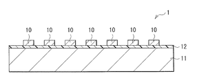
- FIG. 1 schematically illustrates the configuration of an electronic device (electronic device 1) according to an embodiment of the present disclosure.
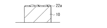
- FIG. 2 schematically shows the configuration of the resin layer 22 a formed on the element portion 10.
- the electronic device 1 is, for example, a display device such as an LED display or a solid-state imaging device.
- the element unit 10 includes, for example, a light emitting element.
- the light emitting element is, for example, a light emitting diode (LED: Light Emitting Diode) chip that emits light of any one of red (R), green (G), and blue (B) is covered with a protective film.
- These element portions 10A are arranged with an interval of, for example, about several ⁇ m to several hundred ⁇ m.
- These element portions 10 are arranged on the first substrate 11 with the adhesive layer 12 interposed therebetween, and are transferred from another substrate (second substrate 21 described later) in the manufacturing process.
- the element unit 10 includes a light receiving element (photoelectric conversion element) such as a photodiode.
- the element unit 10 is not limited to these light emitting elements and light receiving elements, and may be configured to include other various semiconductor elements.
- a resin layer 22a is formed at least partially.
- the resin layer 22a is formed on the element portion 10 after a peeling step by laser ablation described later (a part of the peeling layer 22 described later).
- the resin layer 22 a may be formed only on a part of the element unit 10, or may be formed only on the selective element unit 10 among the plurality of element units 10. Moreover, when removing this resin layer 22a after peeling, the resin layer 22a does not need to be formed on the element part 10.
- the resin layer 22a is made of a resin that has a glass transition point and a thermal decomposition temperature, and is softened, gasified, or plasmaized by absorbing laser light.
- the “thermal decomposition temperature” in the present specification is a temperature at which the mass reduction of the resin starts when the temperature is gradually increased.
- the resin used for the resin layer 22a has a difference between the glass transition point and the thermal decomposition temperature of 150 degrees (° C.) or less.
- Examples of the resin in which the difference between the glass transition point and the thermal decomposition temperature is 150 ° C. or less include a polymer material (cardo type resin) having a cardo structure shown in Chemical Formula 1 below.
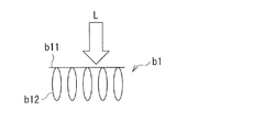
- the cardo structure has a hinge-like structure in which four aromatic rings are bonded to one carbon atom.
- the workability (or transferability) is emphasized.
- an interlayer film such as resin formed around the resin to induce softening of the interlayer resin.
- a resin is selected as the constituent material of the resin layer 22a so that the difference between the glass transition point and the thermal decomposition temperature is 150 degrees or less.
- the resin which comprises the resin layer 22a it is desirable that the vapor pressure at the room temperature in the oxide, nitride, and carbide
- this thermal decomposition temperature (for example, the temperature at which 5% mass reduction starts) is 350 degrees or less. This is because the activation energy described later tends to decrease as the thermal decomposition temperature decreases.
- An example of the resin constituting the resin layer 22a is a cardo type acrylic resin having a glass transition point of 220 degrees and a thermal decomposition temperature of 320 degrees.
- a fluorene derivative can be given as a resin material having a high glass transition point and a low thermal decomposition temperature. Specifically, phenol having a basic structure (cardo structure) of a fluorene derivative, an acrylate of a fluorene derivative, or the like can be given.
- the first substrate 11 is composed of a printed circuit board such as an interposer, for example. On the first substrate 11, in addition to the element unit 10, a driving IC for the element unit 10 and the like are arranged.
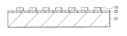
- the electronic device 1 can be formed as follows, for example. 3A to 7 are schematic diagrams for explaining a method of forming the element portion 10A.
- the release layer 22 is made of a resin that is ablated and gasified by absorbing laser light and has a difference between the glass transition point and the thermal decomposition temperature of 150 degrees or less.
- the thickness of the release layer 22 is, for example, 100 nm or more and 5 ⁇ m or less.
- the release layer 22 is more preferably configured so as not to include atoms whose vapor pressure at room temperature of the oxides, nitrides, and carbides is smaller than atmospheric pressure, and the thermal decomposition temperature is, for example, 350 degrees or less.
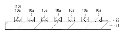
- a second substrate 21 different from the first substrate 11 is prepared, and after the release layer 22 is formed on the second substrate 21, the element portion 10a is formed.
- the second substrate 21 is made of a material (for example, quartz) that transmits the wavelength of the laser light.
- a metal wiring layer is formed on the release layer 22 by plating, and plating bonding is performed. Can be formed.
- solder bumps may be formed on the back surface of the element portion 10a, and solder bonding may be used.
- an adhesive layer may be formed on the release layer 22 and adhered.
- each element portion 10a formed on the second substrate 21 is covered with a protective film (not shown), for example, and molded.
- the protective film is made of a material that transmits light that is emitted (or received).
- an appropriate material should just be selected from a viewpoint of reliability, such as moisture permeability.
- each element unit 10a is individually separated.
- the separation method is not particularly limited, and examples thereof include dry etching using a photolithography method.
- the plurality of element portions 10 a are formed on the second substrate 21 in a two-dimensional arrangement while being separated from each other.
- 3A corresponds to a cross-sectional view taken along the line AA in FIG. 3B.
- the first substrate 11 described above is prepared, and the adhesive layer 12 is formed on the first substrate 11.
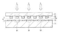
- a second substrate 21 having a plurality of element portions 10a formed thereon is arranged to face the first substrate 11 (specifically, the adhesive layer 12).
- the element portion 10a is arranged between the first substrate 11 and the second substrate 21, and the first substrate 11 and the second substrate 21 are (in detail, the adhesive layer 12 and the element portion 10a are
- the first substrate 11 and the second substrate 21 are arranged to face each other so as to be spaced apart (via the gap d). At least one of the first substrate 11 and the second substrate 21 is held on a movable stage and is driven to be fixed at the predetermined position.
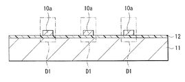
- the peeling layer 22 is irradiated with the laser beam L only in the region D1 corresponding to the selective element portion 10a, for example.
- the laser beam L is irradiated from the second substrate 21 side.
- the wavelength of the laser light L a wavelength that is selectively absorbed by the release layer 22 while being transmitted through the second substrate 21 is selected.
- the irradiation diameter, the output intensity, and the like are set so that the laser beam L is uniformly irradiated on the entire surface of the release layer 22 in the region D1.
- the laser light source include an excimer laser having an output wavelength of 248 nm, a YAG laser having an output wavelength of 266 nm, and the like.
- the peeling layer 22 in the region D1 is gasified (ablated), and as a result, the element portion 10a in the region D1 is peeled from the second substrate 21. Then, it drops onto the adhesive layer 12 immediately below and is fixed by the adhesive layer 12 as it is. Thereafter, the second substrate 21 is separated from the first substrate 11. In this manner, the selective element portion 10a can be transferred onto the first substrate 11 from the second substrate 21 by laser ablation using the release layer 22 (FIG. 6).
- a part of the resin constituting the peeling layer 22 in the region D1 is not gasified and remains on the element portion 10a as a solid (at least on a part of the element portion 10a). Resin layer 22a is formed).
- the resin layer 22a formed on the element portion 10 after the laser irradiation may be removed by adding a process such as dry etching.
- the element unit 10a formed on the second substrate 21 corresponds to a specific example of “first element unit” of the present disclosure.
- the selective element portion 10 (for the sake of explanation) from another substrate (the substrate on which the plurality of element portions 10 are formed as in the second substrate 21). , Referred to as the element portion 10b), and is transferred to the region D2 on the first substrate 11. Thereby, the electronic device shown in FIG. 1 is completed.
- the separation layer 22 to be laser ablated has a difference between the glass transition point and the thermal decomposition temperature. It is comprised with resin used as predetermined temperature or less. Such a configuration has the following effects.
- CRC-8300 (trade name: manufactured by Sumitomo Bakelite Co., Ltd.) is laser ablated is shown in FIG.
- CRC-8300 (trade name: manufactured by Sumitomo Bakelite Co., Ltd.) is a polyimide-based photosensitive resin having a glass transition point of 295 degrees and a thermal decomposition temperature of 540 degrees. That is, the resin used in the comparative example has a difference between the glass transition point and the thermal decomposition temperature of 245 degrees, which is larger than 150 degrees.
- FIG. Show a photograph of a chip side surface after ablation when a cardo type acrylic resin having a glass transition point of 220 degrees and a thermal decomposition temperature of 320 degrees is laser ablated is shown in FIG. Show.
- FIG. Show a photograph of a chip side surface after ablation when a cardo type acrylic resin having a glass transition point of 220 degrees and a thermal decomposition temperature of 320 degrees is laser ablated.
- FIG. Show a photograph of a chip side surface after ablation when a cardo type acrylic resin having a glass transition point of 220 degrees and a thermal decomposition temperature of 320 degrees is laser ablated.
- the scraps after peeling by laser ablation. can be suppressed.
- the polyimide resin used in the comparative example has a structure b100 in which the side chain is formed in a complicated manner, so that the thermal decomposition temperature is high (540 degrees). Therefore, the resin is not easily decomposed by the energy of the laser beam.
- the softening (fluidization) temperature range of the resin is increased, and the softened portion is likely to solidify and become waste as schematically shown in FIG. 10B (b100a).
- the thermal decomposition temperature is low (320 degrees) because the main chain b11 has a cardo structure b1 with a bulky side chain b12.
- the heat resistance is increased (glass transition point 220 degrees).
- the resin is easily decomposed by the energy of the laser beam, and the softening temperature range of the resin is reduced.
- FIG. 11B less waste is generated from the softened portion (b1a).
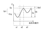
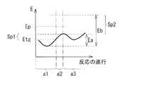
- the state (phase, form) of the resin greatly changes depending on the energy given from the outside, as shown in FIG.
- the resin that is solid at room temperature changes in the order of solid a1, fluid (liquid) a2, and gas a3 in accordance with the energy input from the outside by light or heat.
- the gas a3 is a state in which the resin is decomposed, specifically, a state in which the side chain of the resin is cut by energy from the outside, reacts with oxygen in the atmosphere, and changes into a gas such as carbon dioxide.
- the boundary at which the resin changes from the fluid a2 to the gas a3 is determined by the activation energy Ea.
- the thermal decomposition temperature itself and the difference between the glass transition point and the thermal decomposition temperature are important as physical property parameters.
- the reason is as follows. That is, as in the comparative example shown in FIG. 13, when the difference between the thermal decomposition temperature and the glass transition point is large, since the activation energy Ea is large, the state change of the resin is caused by the energy Eb input from the outside. Is high, the probability of becoming fluid a2 is high (Sp1 in FIG. 13). Further, the possibility of becoming a plasma state is very low (Sp2 in FIG. 13).
- the activation energy Ea is smaller than that of the comparative example as shown in FIG.
- the probability of becoming the fluid a2 is reduced (Sp1 in FIG. 14).
- the gas is gasified to be in a plasma state (Sp2 in FIG. 14).
- the resin is turned into plasma by laser ablation, and it becomes easy to react with oxygen in the atmosphere, so that gasification is promoted. Therefore, at the time of laser ablation, the scattered matter of the resin in the fluid state as in the comparative example can be reduced, and it can be suppressed that the resin adheres to the peripheral structure as waste.
- oxide (SiO 2 ) or nitride (SiN) is generated. Since these compounds have a low vapor pressure, they are not gasified, but are scattered around in a high temperature state, and adhere to the surrounding structure while taking in the decomposed C and the like floating around. The adhesion of such deposits is high and difficult to remove. Therefore, the resin does not contain atoms that generate oxides, nitrides and carbides with such a low vapor pressure as constituent atoms (the vapor pressures of oxides, nitrides and carbides of atoms contained in the resin are high). It becomes possible to gasify most of the constituent elements of the resin.
- ⁇ Modification 1> the method of transferring the selective element portion 10 (10a) of the plurality of element portions 10 on the first substrate 11 from another substrate (second substrate 21) has been described. Laser ablation using such a resin can also be applied to other processes.
- the resin mentioned above may be used for the peeling layer at the time of peeling and transferring after bonding the element part 10 like this modification.
- symbol is attached
- the element portion 10 is formed on the second substrate 21 via the release layer 22.
- the formation method of the element portion 10 various methods such as plating bonding, solder bonding, or adhesion can be used as in the above embodiment.
- the release layer 22 may be formed for each element unit 10 or may be formed on the entire surface of the second substrate 21.
- the first substrate 11 (specifically, the adhesive layer 12) and the second substrate 21 formed with a plurality of element portions 10 are bonded together.
- the first substrate 11 and the second substrate 21 are bonded to each other so that the element unit 10 is disposed between the first substrate 11 and the second substrate 21.
- At least one of the first substrate 11 and the second substrate 21 is held on a movable stage and is driven to be fixed at the predetermined position.
- the release layer 22 is irradiated with the laser light L.
- the laser beam L is irradiated from the second substrate 21 side.
- the wavelength of the laser light L a wavelength that is selectively absorbed by the release layer 22 while being transmitted through the second substrate 21 is selected. Further, the irradiation diameter, the output intensity, and the like are set so that the laser beam L is uniformly irradiated on the entire surface of the release layer 22.
- the release layer 22 is gasified (ablated), and as a result, the plurality of element portions 10 are peeled from the second substrate 21, and the adhesive layer directly below It drops onto 12 and is fixed by the adhesive layer 12 as it is. Thereafter, the second substrate 21 is separated from the first substrate 11. As described above, the plurality of element units 10 can be transferred from the second substrate 21 onto the first substrate 11 by laser ablation using the release layer 22.
- a part of the resin constituting the peeling layer 22 is not gasified and remains on the element part 10a as a solid (the resin layer 22a is at least partially on the element part 10a). Is formed).
- the resin layer 22a may be removed as in the above embodiment.
- the resin phase change during ablation can be obtained by using the same resin as that of the above embodiment for the peeling layer 22. In this case, softening can be suppressed. Therefore, an effect equivalent to that of the above embodiment can be obtained.
- the element unit 10 includes a light emitting element or a light receiving element
- the element unit of the present disclosure is not limited to these light emitting elements and the like, and other semiconductor elements May be included.
- the semiconductor element includes a thin film transistor and a resistance element.
- a conductive film such as a wiring may be included.
- the resin of the present disclosure can be used for a release layer when a pattern of a wiring (conductive film) is transferred and formed by laser ablation.
- laser ablation at the time of transferring the element portion in the electronic device manufacturing process is given as an example.
- laser ablation using the resin of the present disclosure is also applicable to other processes.
- the resin of the present disclosure may be used as a base resin when trimming is performed by laser ablation on a wiring board whose base is made of resin.
- the present invention can be widely applied to direct resin patterning by laser ablation and other processes for processing a resin using a laser.
- the present disclosure may be configured as follows.
- a plurality of the element portions are disposed on the first substrate, The electronic device according to any one of (1) to (4), wherein the element section includes a light emitting element or a light receiving element. (6) The electronic device according to any one of (1) to (5), wherein the element portion is a conductive film. (7) When transferring one or more element units from the second substrate onto the first substrate, A part or all of the one or more element parts are formed on the second substrate via a resin layer, The element portion formed on the second substrate is peeled from the second substrate by laser irradiation to the resin layer and disposed on the first substrate, and the resin layer has a glass transition point and thermal decomposition. The manufacturing method of an electronic device using resin whose difference with temperature is 150 degrees or less.
Landscapes
- Laser Beam Processing (AREA)
- Solid State Image Pick-Up Elements (AREA)
- Die Bonding (AREA)
- Led Device Packages (AREA)
- Light Receiving Elements (AREA)
- Physics & Mathematics (AREA)
- Electromagnetism (AREA)
Abstract
Description
1.実施の形態(選択的な素子部を移載する際のレーザアブレーション用の剥離層として、ガラス転移点と熱分解温度との差が150度以下となる樹脂を用いた電子デバイスの例)
・構成
・製造方法
・作用、効果
2.変形例1(複数の素子部を貼り合わせ後に剥離して移載する場合の例)
[構成]
図1は、本開示の一実施の形態に係る電子デバイス(電子デバイス1)の構成を模式的に表したものである。図2は、素子部10上に形態された樹脂層22aの構成を模式的に表したものである。電子デバイス1は、第1基板11上に、接着層12を介して複数の素子部10が配置されたものである。この電子デバイス1は、例えばLEDディスプレイなどの表示装置、または固体撮像装置などである。

電子デバイス1は、例えば次のようにして形成することができる。図3A~図7は、素子部10Aの形成方法を説明するための模式図である。
本実施の形態では、電子デバイス1の製造プロセスにおいて、第1基板11上に素子部10を移載する際に、レーザアブレーションされる剥離層22が、ガラス転移点と熱分解温度との差が所定の温度以下となる樹脂により構成されている。このような構成により、次のような効果がある。
上記実施の形態では、第1基板11上の複数の素子部10のうちの選択的な素子部10(10a)を他の基板(第2基板21)から移載する手法について述べたが、上述したような樹脂を用いたレーザアブレーションは、他のプロセスにも適用することができる。例えば、本変形例のように、素子部10を貼り合わせ後に剥離して移載する際の剥離層に上述した樹脂が用いられてもよい。尚、上記実施の形態と同様の構成要素については同一の符号を付し、その説明を省略する。
(1)
第1基板上に配置された1または複数の素子部と、
各素子部上の少なくとも一部に形成された樹脂層と
を備え、
前記樹脂層は、ガラス転移点と熱分解温度との差が150度以下である樹脂から構成されている
電子デバイス。
(2)
前記樹脂に含まれる原子は、その酸化物、窒化物および炭化物における蒸気圧が大気圧以上である
上記(1)に記載の電子デバイス。
(3)
前記熱分解温度は350度以下である
上記(1)または(2)に記載の電子デバイス。
(4)
前記樹脂は、カルド構造をもつ高分子材料である
上記(1)ないし(3)のいずれか1つに記載の電子デバイス。
(5)
前記素子部が前記第1基板上に複数配置され、
前記素子部は発光素子または受光素子を含む
上記(1)ないし(4)のいずれか1つに記載の電子デバイス。
(6)
前記素子部は導電膜である
上記(1)ないし(5)のいずれか1つに記載の電子デバイス。
(7)
第1基板上に1または複数の素子部を第2基板から移載する際に、
前記1または複数の素子部のうちの一部または全部の素子部を、第2基板上に樹脂層を介して形成し、
前記第2基板上に形成された素子部を、前記樹脂層へのレーザ照射により前記第2基板から剥離して前記第1基板上に配置し、かつ
前記樹脂層として、ガラス転移点と熱分解温度との差が150度以下である樹脂を用いた
電子デバイスの製造方法。
(8)
前記樹脂に含まれる原子は、その酸化物、窒化物および炭化物における蒸気圧が大気圧
以上である
上記(7)に記載の電子デバイスの製造方法。
(9)
前記熱分解温度は350度以下である
上記(7)または(8)に記載の電子デバイスの製造方法。
(10)
前記複数の素子部のうちの一部の素子部に相当する第1素子部が、前記第2基板上に前記樹脂層を介して複数形成され、
前記第1素子部が複数形成された第2基板が、前記第1素子部を間にして前記第1基板に対向して配置され、
前記第2基板が前記第1基板に対向配置された後、前記複数の第1素子部のうちの選択的な第1素子部に対応する領域においてレーザ光が前記樹脂層に照射される
上記(7)ないし(9)のいずれか1つに記載の電子デバイスの製造方法。
(11)
前記レーザ光の照射後、前記第1素子部の上に形成された樹脂層を除去する
上記(10)に記載の電子デバイスの製造方法。
(12)
前記複数の素子部が、前記第2基板上に樹脂層を介して形成され、
前記複数の素子部が形成された第2基板が、前記複数の素子部を間にして前記第1基板に貼り合わせられ、
前記第2基板が前記第1基板に貼り合わせられた後、レーザ光が前記樹脂層に照射される
上記(7)ないし(11)のいずれか1つに記載の電子デバイスの製造方法。
(13)
前記レーザ光の照射後、前記素子部の上に形成された樹脂層を除去する
上記(12)に記載の電子デバイスの製造方法。
(14)
前記樹脂は、カルド構造をもつ高分子材料である
上記(7)ないし(13)のいずれか1つに記載の電子デバイスの製造方法。
(15)
前記素子部は発光素子または受光素子を含む
上記(7)ないし(14)のいずれか1つ記載の電子デバイスの製造方法。
(16)
前記素子部は導電膜である
上記(7)ないし(15)のいずれか1つに記載の電子デバイスの製造方法。
Claims (16)
- 第1基板上に配置された1または複数の素子部と、
各素子部上の少なくとも一部に形成された樹脂層と
を備え、
前記樹脂層は、ガラス転移点と熱分解温度との差が150度以下である樹脂から構成されている
電子デバイス。 - 前記樹脂に含まれる原子は、その酸化物、窒化物および炭化物における蒸気圧が大気圧以上である
請求項1に記載の電子デバイス。 - 前記熱分解温度は350度以下である
請求項1に記載の電子デバイス。 - 前記樹脂は、カルド構造をもつ高分子材料である
請求項1に記載の電子デバイス。 - 前記素子部が前記第1基板上に複数配置され、
前記素子部は発光素子または受光素子を含む
請求項1に記載の電子デバイス。 - 前記素子部は導電膜である
請求項1に記載の電子デバイス。 - 第1基板上に1または複数の素子部を第2基板から移載する際に、
前記1または複数の素子部のうちの一部または全部の素子部を、第2基板上に樹脂層を介して形成し、
前記第2基板上に形成された素子部を、前記樹脂層へのレーザ照射により前記第2基板から剥離して前記第1基板上に配置し、かつ
前記樹脂層として、ガラス転移点と熱分解温度との差が150度以下である樹脂を用いた
電子デバイスの製造方法。 - 前記樹脂に含まれる原子は、その酸化物、窒化物および炭化物における蒸気圧が大気圧以上である
請求項7に記載の電子デバイスの製造方法。 - 前記熱分解温度は350度以下である
請求項7に記載の電子デバイスの製造方法。 - 前記複数の素子部のうちの一部の素子部に相当する第1素子部が、前記第2基板上に前記樹脂層を介して複数形成され、
前記第1素子部が複数形成された第2基板が、前記第1素子部を間にして前記第1基板に対向して配置され、
前記第2基板が前記第1基板に対向配置された後、前記複数の第1素子部のうちの選択的な第1素子部に対応する領域においてレーザ光が前記樹脂層に照射される
請求項7に記載の電子デバイスの製造方法。 - 前記レーザ光の照射後、前記第1素子部の上に形成された樹脂層を除去する
請求項10に記載の電子デバイスの製造方法。 - 前記複数の素子部が、前記第2基板上に樹脂層を介して形成され、
前記複数の素子部が形成された第2基板が、前記複数の素子部を間にして前記第1基板に貼り合わせられ、
前記第2基板が前記第1基板に貼り合わせられた後、レーザ光が前記樹脂層に照射される
請求項7に記載の電子デバイスの製造方法。 - 前記レーザ光の照射後、前記素子部の上に形成された樹脂層を除去する
請求項12に記載の電子デバイスの製造方法。 - 前記樹脂は、カルド構造をもつ高分子材料である
請求項7に記載の電子デバイスの製造方法。 - 前記素子部は発光素子または受光素子を含む
請求項7記載の電子デバイスの製造方法。 - 前記素子部は導電膜である
請求項7に記載の電子デバイスの製造方法。
Priority Applications (4)
| Application Number | Priority Date | Filing Date | Title |
|---|---|---|---|
| JP2017509475A JP6738802B2 (ja) | 2015-03-30 | 2016-03-09 | 電子デバイスおよび電子デバイスの製造方法 |
| KR1020177026274A KR20170133345A (ko) | 2015-03-30 | 2016-03-09 | 전자 디바이스 및 전자 디바이스의 제조 방법 |
| CN201680017583.6A CN107408607B (zh) | 2015-03-30 | 2016-03-09 | 电子装置以及制造电子装置的方法 |
| US15/560,207 US10424501B2 (en) | 2015-03-30 | 2016-03-09 | Electronic device and method of manufacturing electronic device |
Applications Claiming Priority (2)
| Application Number | Priority Date | Filing Date | Title |
|---|---|---|---|
| JP2015069261 | 2015-03-30 | ||
| JP2015-069261 | 2015-03-30 |
Publications (1)
| Publication Number | Publication Date |
|---|---|
| WO2016158264A1 true WO2016158264A1 (ja) | 2016-10-06 |
Family
ID=57004230
Family Applications (1)
| Application Number | Title | Priority Date | Filing Date |
|---|---|---|---|
| PCT/JP2016/057352 Ceased WO2016158264A1 (ja) | 2015-03-30 | 2016-03-09 | 電子デバイスおよび電子デバイスの製造方法 |
Country Status (5)
| Country | Link |
|---|---|
| US (1) | US10424501B2 (ja) |
| JP (1) | JP6738802B2 (ja) |
| KR (1) | KR20170133345A (ja) |
| CN (1) | CN107408607B (ja) |
| WO (1) | WO2016158264A1 (ja) |
Cited By (10)
| Publication number | Priority date | Publication date | Assignee | Title |
|---|---|---|---|---|
| WO2019207920A1 (ja) * | 2018-04-26 | 2019-10-31 | Jsr株式会社 | 半導体素子の実装方法および実装装置 |
| JP2020096144A (ja) * | 2018-12-14 | 2020-06-18 | Tdk株式会社 | 素子アレイの製造方法と特定素子の除去方法 |
| WO2020166301A1 (ja) * | 2019-02-14 | 2020-08-20 | 東レエンジニアリング株式会社 | 半導体チップの支持基板、転写装置および転写方法 |
| JP2020188037A (ja) * | 2019-05-09 | 2020-11-19 | 三星電子株式会社Samsung Electronics Co.,Ltd. | ディスプレイ装置の製造方法、およびソース基板構造体 |
| JP2022506167A (ja) * | 2018-10-29 | 2022-01-17 | オスラム オプト セミコンダクターズ ゲゼルシャフト ミット ベシュレンクテル ハフツング | オプトエレクトロニクス半導体コンポーネントの製造方法 |
| KR20220050057A (ko) | 2020-10-15 | 2022-04-22 | 닛테츠 케미컬 앤드 머티리얼 가부시키가이샤 | 적층체의 제조 방법 및 처리 방법, 그 제조 방법 및 처리 방법에서 사용하는 감광성 수지 조성물 |
| KR20220050788A (ko) | 2020-10-15 | 2022-04-25 | 닛테츠 케미컬 앤드 머티리얼 가부시키가이샤 | 접착제층 형성용 조성물, 적층체의 제조 방법 및 처리 방법 |
| KR20230147535A (ko) | 2022-04-14 | 2023-10-23 | 닛테츠 케미컬 앤드 머티리얼 가부시키가이샤 | 수지 조성물, 적층체의 제조 방법, 적층체 및 처리 방법 |
| JP2024001969A (ja) * | 2022-06-23 | 2024-01-11 | 日亜化学工業株式会社 | 発光装置の製造方法 |
| WO2025069762A1 (ja) * | 2023-09-29 | 2025-04-03 | 信越化学工業株式会社 | 移載方法 |
Families Citing this family (1)
| Publication number | Priority date | Publication date | Assignee | Title |
|---|---|---|---|---|
| CN108807265B (zh) * | 2018-07-09 | 2020-01-31 | 厦门乾照光电股份有限公司 | Micro-LED巨量转移方法、显示装置及制作方法 |
Citations (4)
| Publication number | Priority date | Publication date | Assignee | Title |
|---|---|---|---|---|
| JP2002314053A (ja) * | 2001-04-19 | 2002-10-25 | Sony Corp | チップ部品の転写方法及びこれを用いた素子の配列方法、画像表示装置の製造方法 |
| JP2004184754A (ja) * | 2002-12-04 | 2004-07-02 | Sony Corp | フラットパネルディスプレイの製造方法 |
| JP2004228373A (ja) * | 2003-01-23 | 2004-08-12 | Seiko Epson Corp | デバイスの製造方法とデバイス、電気光学装置、及び電子機器 |
| JP2010251359A (ja) * | 2009-04-10 | 2010-11-04 | Sony Corp | 素子の移載方法 |
Family Cites Families (2)
| Publication number | Priority date | Publication date | Assignee | Title |
|---|---|---|---|---|
| US8772939B2 (en) * | 2008-08-04 | 2014-07-08 | Micron Technology, Inc. | Polishing systems and methods for removing conductive material from microelectronic substrates |
| JP5580800B2 (ja) * | 2010-10-29 | 2014-08-27 | 東京応化工業株式会社 | 積層体、およびその積層体の分離方法 |
-
2016
- 2016-03-09 US US15/560,207 patent/US10424501B2/en active Active
- 2016-03-09 JP JP2017509475A patent/JP6738802B2/ja not_active Expired - Fee Related
- 2016-03-09 WO PCT/JP2016/057352 patent/WO2016158264A1/ja not_active Ceased
- 2016-03-09 KR KR1020177026274A patent/KR20170133345A/ko not_active Withdrawn
- 2016-03-09 CN CN201680017583.6A patent/CN107408607B/zh not_active Expired - Fee Related
Patent Citations (4)
| Publication number | Priority date | Publication date | Assignee | Title |
|---|---|---|---|---|
| JP2002314053A (ja) * | 2001-04-19 | 2002-10-25 | Sony Corp | チップ部品の転写方法及びこれを用いた素子の配列方法、画像表示装置の製造方法 |
| JP2004184754A (ja) * | 2002-12-04 | 2004-07-02 | Sony Corp | フラットパネルディスプレイの製造方法 |
| JP2004228373A (ja) * | 2003-01-23 | 2004-08-12 | Seiko Epson Corp | デバイスの製造方法とデバイス、電気光学装置、及び電子機器 |
| JP2010251359A (ja) * | 2009-04-10 | 2010-11-04 | Sony Corp | 素子の移載方法 |
Cited By (16)
| Publication number | Priority date | Publication date | Assignee | Title |
|---|---|---|---|---|
| WO2019207920A1 (ja) * | 2018-04-26 | 2019-10-31 | Jsr株式会社 | 半導体素子の実装方法および実装装置 |
| JP2022506167A (ja) * | 2018-10-29 | 2022-01-17 | オスラム オプト セミコンダクターズ ゲゼルシャフト ミット ベシュレンクテル ハフツング | オプトエレクトロニクス半導体コンポーネントの製造方法 |
| US12112968B2 (en) | 2018-10-29 | 2024-10-08 | Osram Opto Semiconductors Gmbh | Method for producing optoelectronic devices |
| JP2020096144A (ja) * | 2018-12-14 | 2020-06-18 | Tdk株式会社 | 素子アレイの製造方法と特定素子の除去方法 |
| US11101317B2 (en) | 2018-12-14 | 2021-08-24 | Tdk Corporation | Method of manufacturing element array and method of removing specific element |
| JP2021180317A (ja) * | 2018-12-14 | 2021-11-18 | Tdk株式会社 | 素子アレイの製造方法と特定素子の除去方法 |
| JP7173228B2 (ja) | 2018-12-14 | 2022-11-16 | Tdk株式会社 | 素子アレイの製造方法と特定素子の除去方法 |
| WO2020166301A1 (ja) * | 2019-02-14 | 2020-08-20 | 東レエンジニアリング株式会社 | 半導体チップの支持基板、転写装置および転写方法 |
| JP7321760B2 (ja) | 2019-05-09 | 2023-08-07 | 三星電子株式会社 | ディスプレイ装置の製造方法、およびソース基板構造体 |
| JP2020188037A (ja) * | 2019-05-09 | 2020-11-19 | 三星電子株式会社Samsung Electronics Co.,Ltd. | ディスプレイ装置の製造方法、およびソース基板構造体 |
| KR20220050788A (ko) | 2020-10-15 | 2022-04-25 | 닛테츠 케미컬 앤드 머티리얼 가부시키가이샤 | 접착제층 형성용 조성물, 적층체의 제조 방법 및 처리 방법 |
| KR20220050057A (ko) | 2020-10-15 | 2022-04-22 | 닛테츠 케미컬 앤드 머티리얼 가부시키가이샤 | 적층체의 제조 방법 및 처리 방법, 그 제조 방법 및 처리 방법에서 사용하는 감광성 수지 조성물 |
| KR20230147535A (ko) | 2022-04-14 | 2023-10-23 | 닛테츠 케미컬 앤드 머티리얼 가부시키가이샤 | 수지 조성물, 적층체의 제조 방법, 적층체 및 처리 방법 |
| JP2024001969A (ja) * | 2022-06-23 | 2024-01-11 | 日亜化学工業株式会社 | 発光装置の製造方法 |
| JP7842954B2 (ja) | 2022-06-23 | 2026-04-09 | 日亜化学工業株式会社 | 発光装置の製造方法 |
| WO2025069762A1 (ja) * | 2023-09-29 | 2025-04-03 | 信越化学工業株式会社 | 移載方法 |
Also Published As
| Publication number | Publication date |
|---|---|
| CN107408607A (zh) | 2017-11-28 |
| US10424501B2 (en) | 2019-09-24 |
| KR20170133345A (ko) | 2017-12-05 |
| JP6738802B2 (ja) | 2020-08-12 |
| US20180047608A1 (en) | 2018-02-15 |
| JPWO2016158264A1 (ja) | 2018-02-22 |
| CN107408607B (zh) | 2019-10-29 |
Similar Documents
| Publication | Publication Date | Title |
|---|---|---|
| JP6738802B2 (ja) | 電子デバイスおよび電子デバイスの製造方法 | |
| KR101995141B1 (ko) | 배선 기판, 반도체 장치 및 반도체 장치의 제조 방법 | |
| JP4959422B2 (ja) | ウエーハの分割方法 | |
| JP2010062527A (ja) | 薄膜素子の製造方法 | |
| JP6113529B2 (ja) | ウエーハの加工方法 | |
| US8293583B2 (en) | Method for manufacturing semiconductor device | |
| JP2006049800A (ja) | 薄膜デバイスの供給体、薄膜デバイスの供給体の製造方法、転写方法、半導体装置の製造方法及び電子機器 | |
| TW201227937A (en) | Image sensor chip package and method for forming the same | |
| TWI910284B (zh) | 附支持體之基板單元、基板單元、及附支持體之基板單元的製造方法 | |
| US11895780B2 (en) | Manufacturing method of package structure | |
| JP2017050464A (ja) | 配線基板積層体、その製造方法及び半導体装置の製造方法 | |
| CN118302848A (zh) | 具有激光释放层的硅分选器 | |
| JP5726110B2 (ja) | 半導体装置及びその製造方法並びに電子機器 | |
| JP5324821B2 (ja) | 半導体装置の製造方法 | |
| JP2009095962A (ja) | 薄膜半導体装置の製造方法 | |
| CN105140206B (zh) | 基板结构及其制作方法 | |
| US11659669B2 (en) | Multi-step integrated circuit handling process and apparatus | |
| JP2010056319A (ja) | 半導体装置の製造方法および半導体装置 | |
| JP5372112B2 (ja) | 配線基板の製造方法及び半導体パッケージの製造方法 | |
| JP6447073B2 (ja) | 配線基板及びラミネート装置 | |
| JP2007286600A (ja) | 薄膜素子の転写方法、転写体、転写生成物、回路基板及び表示装置 | |
| US20160050761A1 (en) | Substrate structure and method of manuifacturing the same | |
| JP2003203881A (ja) | 電子部品の剥離方法及びその実装方法 | |
| JP6447075B2 (ja) | 配線基板、半導体装置及び半導体装置の製造方法 | |
| JP2007227726A (ja) | 集合基板加工方法 |
Legal Events
| Date | Code | Title | Description |
|---|---|---|---|
| 121 | Ep: the epo has been informed by wipo that ep was designated in this application |
Ref document number: 16772148 Country of ref document: EP Kind code of ref document: A1 |
|
| ENP | Entry into the national phase |
Ref document number: 20177026274 Country of ref document: KR Kind code of ref document: A |
|
| ENP | Entry into the national phase |
Ref document number: 2017509475 Country of ref document: JP Kind code of ref document: A |
|
| WWE | Wipo information: entry into national phase |
Ref document number: 15560207 Country of ref document: US |
|
| NENP | Non-entry into the national phase |
Ref country code: DE |
|
| 122 | Ep: pct application non-entry in european phase |
Ref document number: 16772148 Country of ref document: EP Kind code of ref document: A1 |