WO2016152581A1 - 透明導電性基板及び透明積層構造体 - Google Patents
透明導電性基板及び透明積層構造体 Download PDFInfo
- Publication number
- WO2016152581A1 WO2016152581A1 PCT/JP2016/057770 JP2016057770W WO2016152581A1 WO 2016152581 A1 WO2016152581 A1 WO 2016152581A1 JP 2016057770 W JP2016057770 W JP 2016057770W WO 2016152581 A1 WO2016152581 A1 WO 2016152581A1
- Authority
- WO
- WIPO (PCT)
- Prior art keywords
- film
- transparent conductive
- transparent
- substrate
- conductive substrate
- Prior art date
- Legal status (The legal status is an assumption and is not a legal conclusion. Google has not performed a legal analysis and makes no representation as to the accuracy of the status listed.)
- Ceased
Links
Images












Classifications
-
- G—PHYSICS
- G06—COMPUTING OR CALCULATING; COUNTING
- G06F—ELECTRIC DIGITAL DATA PROCESSING
- G06F3/00—Input arrangements for transferring data to be processed into a form capable of being handled by the computer; Output arrangements for transferring data from processing unit to output unit, e.g. interface arrangements
- G06F3/01—Input arrangements or combined input and output arrangements for interaction between user and computer
- G06F3/03—Arrangements for converting the position or the displacement of a member into a coded form
- G06F3/041—Digitisers, e.g. for touch screens or touch pads, characterised by the transducing means
-
- H—ELECTRICITY
- H01—ELECTRIC ELEMENTS
- H01B—CABLES; CONDUCTORS; INSULATORS; SELECTION OF MATERIALS FOR THEIR CONDUCTIVE, INSULATING OR DIELECTRIC PROPERTIES
- H01B5/00—Non-insulated conductors or conductive bodies characterised by their form
- H01B5/14—Non-insulated conductors or conductive bodies characterised by their form comprising conductive layers or films on insulating-supports
-
- B—PERFORMING OPERATIONS; TRANSPORTING
- B32—LAYERED PRODUCTS
- B32B—LAYERED PRODUCTS, i.e. PRODUCTS BUILT-UP OF STRATA OF FLAT OR NON-FLAT, e.g. CELLULAR OR HONEYCOMB, FORM
- B32B2307/00—Properties of the layers or laminate
- B32B2307/20—Properties of the layers or laminate having particular electrical or magnetic properties, e.g. piezoelectric
- B32B2307/202—Conductive
-
- B—PERFORMING OPERATIONS; TRANSPORTING
- B32—LAYERED PRODUCTS
- B32B—LAYERED PRODUCTS, i.e. PRODUCTS BUILT-UP OF STRATA OF FLAT OR NON-FLAT, e.g. CELLULAR OR HONEYCOMB, FORM
- B32B2307/00—Properties of the layers or laminate
- B32B2307/40—Properties of the layers or laminate having particular optical properties
- B32B2307/412—Transparent
-
- B—PERFORMING OPERATIONS; TRANSPORTING
- B32—LAYERED PRODUCTS
- B32B—LAYERED PRODUCTS, i.e. PRODUCTS BUILT-UP OF STRATA OF FLAT OR NON-FLAT, e.g. CELLULAR OR HONEYCOMB, FORM
- B32B2307/00—Properties of the layers or laminate
- B32B2307/40—Properties of the layers or laminate having particular optical properties
- B32B2307/416—Reflective
-
- G—PHYSICS
- G06—COMPUTING OR CALCULATING; COUNTING
- G06F—ELECTRIC DIGITAL DATA PROCESSING
- G06F2203/00—Indexing scheme relating to G06F3/00 - G06F3/048
- G06F2203/041—Indexing scheme relating to G06F3/041 - G06F3/045
- G06F2203/04112—Electrode mesh in capacitive digitiser: electrode for touch sensing is formed of a mesh of very fine, normally metallic, interconnected lines that are almost invisible to see. This provides a quite large but transparent electrode surface, without need for ITO or similar transparent conductive material
Definitions
- the present invention relates to a transparent conductive substrate and a transparent laminated structure suitable for touch panel applications. More specifically, the present invention relates to a transparent conductive substrate and a transparent laminated structure in which a sensor electrode of a touch panel is hardly visible.
- This application claims priority based on Japanese Patent Application No. 2015-062735 for which it applied to Japan on March 25, 2015, and uses the content here.
- ITO indium oxide
- a structure in which fine wires of metal members are arranged in a mesh shape on an insulating transparent substrate made of glass or the like or on a transparent conductive film such as ITO is a plasma display panel.
- a transparent conductive film such as ITO
- An electromagnetic shielding film for example, Patent Document 1
- application of the thin wire of the metal member as a sensor electrode for a touch panel has been studied.
- copper (Cu) is frequently used as the material of the metal mesh.
- a metal film such as Cu has a property of easily reflecting light (high reflectance).
- FIG. 8A to 8D are views showing an example of a configuration in which a metal mesh is formed on a transparent substrate
- FIG. 8A is a plan view showing the whole
- FIG. 8B is an enlarged view of a region P5
- FIG. 8D shows a cross-sectional view taken along line ZZ in FIG. 8B.
- reference numeral 501 denotes a transparent base material (transparent substrate)
- reference numeral 502 denotes a metal film.
- a metal film 502F (502) made of Cu is formed on the entire surface of the transparent substrate 501F (501) [FIG. 8D].
- the metal film 502F is etched to form a mesh-like metal film, and then the surface of the metal film is oxidized to obtain the configuration shown in FIG. 8C. It is done.
- the mesh-like Cu electrode 502 is arranged on the glass substrate 501E.
- the Cu electrode 502 includes a part (metal part) 502Ea having characteristics of a metal film formed at the time of film formation of the Cu electrode, and a part (blackened part) 502Eb changed to black by oxidation treatment on the surface of the Cu electrode.
- the surface 502ET of the mesh-like Cu electrode 502 is a blackened portion 502Eb.
- a portion corresponding to the opening of the mesh is the surface 501ET of the glass substrate.
- the oxidation state tends to change with time in the vicinity of the boundary between the metal portion 502Ea and the blackened portion 502Eb. That is, in the Cu electrode 502, since the ratio of the metal part 502Ea and the blackened part 502Eb varies, the conventional metal mesh structure (Cu electrode 502) has a problem that the characteristic (specific resistance) as a conductive film is not stable. I had it. Furthermore, since the oxidation state of the surface of the metal mesh is likely to change, there is also a problem that the degree of change to black is easily changed, and the color of the surface of the metal mesh is easily changed.
- the present invention has been made in view of the above circumstances, and obtains stable conductivity, suppresses reflection light from being recognized by an observer, and has excellent connectivity with an external circuit.
- An object of the present invention is to provide a transparent conductive substrate and a transparent laminated structure having a mesh structure.
- a transparent substrate, an intermediate film that is an oxide film containing molybdenum (Mo), and a transparent conductive film are sequentially laminated on one surface of the transparent substrate.
- a transparent substrate, an intermediate film that is an oxide film containing molybdenum (Mo), and a transparent conductive film are sequentially laminated on one surface of the transparent substrate.
- the reflectance with respect to incident light having a wavelength of 550 nm is 5% or less.
- the intermediate film may have a specific resistance [ ⁇ ⁇ cm] of 1.8 ⁇ 10 8 or less.
- the film thickness [nm] of the transparent conductive film may be in the range of 10 to 50.
- the hue of the structure is changed. It may be adjustable.
- the transparent laminated structure according to the third aspect of the present invention includes a metal film, an intermediate film that is provided on the metal film and is an oxide film containing molybdenum (Mo), and a transparent conductive film provided on the intermediate film. And a membrane.
- Mo molybdenum
- an average reflectance is 10 [%] or less with respect to the incident light of visible light region.
- the transparent conductive substrate according to the above aspect of the present invention includes a structure in which a metal film, an intermediate film, and a transparent conductive film are sequentially laminated on one surface of a transparent substrate, and the intermediate film includes molybdenum (Mo). It consists of an oxide film containing.
- Mo molybdenum
- the transparent conductive substrate according to the above aspect of the present invention has a laminated structure, there is an interface between the metal film and the intermediate film, and oxygen contained in the intermediate film beyond the interface. The risk of entering the metal film is extremely low compared to the conventional configuration (configuration in which the surface of the metal film is oxidized).
- the hue is adjusted by the intermediate film and the transparent conductive film independently of the metal film, the hue (reflection of the structure) is compared to the conventional configuration in which the surface is blackened by oxidation treatment on the surface of the metal film. Characteristics) can be maintained stably.
- the condition that the average reflectance is 10% or less with respect to incident light in the visible light range (wavelength range of 380 to 780 [nm]), or the wavelength of 550 nm that is most brightly visible through human eyes.
- the reflectance satisfies the condition of 5% or less, the structure has a low reflection structure, can be adjusted to a desired color, and also has conductivity as an electrode. Is done.
- the above aspect of the present invention contributes to providing a transparent conductive substrate having a metal mesh structure that obtains stable conductivity and suppresses reflection light from being recognized by an observer.
- FIG. 2 is a cross-sectional view schematically showing an example of a transparent conductive substrate according to an embodiment of the present invention, and is a view taken along line AA in FIG. 1B.
- FIG. 2 is a cross-sectional view schematically showing an example of a transparent conductive substrate according to an embodiment of the present invention, and is a view taken along line AA in FIG. 1B.
- FIG. 1 It is a schematic diagram which shows an example of the manufacturing apparatus of the transparent conductive substrate which concerns on embodiment of this invention. It is a schematic diagram which shows another example of the manufacturing apparatus of the transparent conductive substrate which concerns on embodiment of this invention. It is sectional drawing which shows typically an example of the solar cell which concerns on the modification 1 of embodiment of this invention. It is an expanded sectional view showing typically an example of a solar cell concerning modification 1 of an embodiment of the present invention. It is an expanded sectional view showing typically an example of a solar cell concerning modification 2 of an embodiment of the present invention. It is a top view which shows typically an example of the conventional transparent conductive substrate.
- FIGS. 1C and 1D are diagrams showing a transparent conductive substrate in the present embodiment
- FIG. 1A is an overall plan view
- FIG. 1B is an enlarged plan view of a region P1
- FIGS. 1C and 1D are diagrams.
- 1B shows a cross-sectional view along line AA of 1B.
- FIG. 1C is a cross-sectional view showing the transparent conductive substrate after etching
- FIG. 1D is a cross-sectional view showing the transparent conductive substrate before etching.
- the transparent conductive substrate in the present embodiment is used, for example, for a capacitive touch panel that is disposed on a display panel such as liquid crystal or organic EL (organic electroluminescence) and operated by touching an operation surface.
- a transparent conductive substrate S1E (S1) has a metal film 102E (102), an intermediate film on one surface 101ET of an insulating transparent substrate 101E (101) made of glass or the like.
- 103E (103) and a transparent conductive film 104E (104) are sequentially stacked (transparent laminated structure).
- FIGS. 1A to 1D show an example in which the structure has a mesh shape.
- the side surface shape of the structure is not limited to a structure in which all three layers form the same one side surface, and an uneven structure may be formed on the side surface depending on conditions in an etching process described later.
- the metal film 102E is electrically connected to the drive circuit through the intermediate film 103E and the transparent conductive film 104E laminated on the metal film 102E, and further through the FPC connected to the transparent conductive film 104E.
- the intermediate film 103 is provided at a position between the metal film 102 and the transparent conductive film 104 [the intermediate film 103 is omitted in FIGS. 1A and 1B].
- These three-layer structures are preferably etched together in the manufacturing method described later, but may be etched into each film.
- the transparent substrate 101 for example, in addition to a substrate made of glass, PET (polyethylene terephthalate), PP (polypropylene), PC (polycarbonate).
- PET polyethylene terephthalate
- PP polypropylene
- PC polycarbonate
- COP cycloolefin polymer: Cyclo-olefin polymer
- PE polyethylene: polyethylene
- PMMA Polymethyl methacrylate: polymethyl methacrylate
- the metal film 102 having the above structure is required to have excellent conductivity and high etching property.
- the metal film member that satisfies such conditions include Al, Al alloy, Mo, Mo alloy, Ti, Ti alloy, Cu, and Cu alloy.
- a metal film made of an (Al—Nd) alloy containing neodymium (Nd) in Al is preferable from the viewpoint that stable conductivity and weather resistance can be obtained, and further, a problem peculiar to Al by addition of Nd. It is preferable because the generation of hillocks can be suppressed.
- the intermediate film 103 in the above configuration is used by being disposed between the metal film 102 and the transparent conductive film 104, the conductivity sufficient to ensure conduction between the transparent conductive film and the metal film and reflected light are observed. It is required to have a low reflectance condition necessary for suppressing recognition by a person.
- an oxide film containing molybdenum (Mo) is preferably used as the intermediate film. This is because the good conductivity of molybdenum oxide works effectively for the connection between the metal film and the transparent conductive film. Even when an alloy such as (Mo—Nb) containing niobium (Nb) in Mo is used, the weather resistance can be improved and low reflection can be obtained by adding Nb to the metal film. As conditions, the same effects as those obtained when the alloy is not used can be obtained.
- N 2 may be added slightly in order to adjust the etching rate of the intermediate film.
- the formed intermediate film contains a slight amount of nitrogen, but this addition does not impair the function of the intermediate film as an oxide film.
- the transparent conductive film 104 in the above configuration is not particularly limited, and a known transparent conductive material can be used.
- a known transparent conductive material can be used.
- ITO Indium Tin Oxide
- AZO ZnO doped with Al
- BZO B-doped ZnO
- In 2 O 3 ZnO
- In 2 O 3 —TiO 2 and the like.
- In 2 O 3 By containing In 2 O 3 , a transparent conductive film that is soluble in acid and resistant to alkali can be obtained while maintaining good conductivity.
- a transparent conductive film having such characteristics is suitable for a photolithography process.
- the structure including the three layers, that is, the metal film 102, the intermediate film 103, and the transparent conductive film 104 has an average reflectance with respect to incident light in the visible light region (wavelength region is 380 to 780 [nm]).
- the ratio By setting the ratio to 10 [%] or less, the structure effectively functions as a low reflection structure. For this reason, it becomes possible to adjust the color of the surface of the metal mesh.
- the reflectance is specified to be 5% or less for incident light having a wavelength of 550 [nm] on behalf of the visible light region, the function as a low reflection structure is ensured.
- the transparent conductive material is used so that the reflectance of light reflected by the light having a wavelength of 550 [nm] incident on the structure (transparent laminated structure) is 5 [%] or less.
- the reflectance of the transparent laminated structure provided on the substrate is adjusted. As a result, even when the reflectance increases rapidly in the upper limit region (near 380 nm) or the lower limit region (near 780 nm) of the visible light region, the transparent laminated structure and the transparent conductive substrate provided with this transparent laminated structure Can effectively function as a low reflection structure.
- the average reflectance in the embodiment of the present invention is basically the sum of the reflectance values obtained at 1 nm pitch in the visible light range (wavelength range is 380 to 780 [nm]), It is defined by the numerical value divided by the score of the total data. However, for simplicity, it is defined by a numerical value obtained by adding the reflectances obtained at a 50 nm pitch within the visible light range (wavelength range: 380 to 780 [nm]) and dividing by the total number of data points.
- the number of data points used for calculating the average value is not particularly limited.
- FIG. 3 is a graph showing the reflectance of the structure (transparent laminated structure) in the transparent conductive substrate according to the embodiment of the present invention.
- the horizontal axis represents the wavelength of incident light
- the vertical axis represents the reflectance.
- the solid line in FIG. 3 has shown the result of the transparent laminated structure of the Example which has a 3 layer laminated structure which concerns on embodiment of this invention.
- the dotted line in FIG. 3 has shown the result of the transparent conductive substrate of a comparative example.
- the transparent conductive substrate of the comparative example has a configuration in which the intermediate film and the transparent conductive film are not provided, that is, only the metal film is formed on the substrate.
- the measuring device is arranged on the side opposite to the position where the substrate is arranged, the amount of reflected light is measured, and the reflectance is measured. Went. Specifically, in the case of the example, a measuring device was arranged at a position facing the transparent conductive film, the amount of reflected light was measured, and the reflectance was measured. In the case of the comparative example, a measuring device was disposed at a position facing the metal film, the amount of reflected light was measured, and the reflectance was measured.
- the obtained reflectance value indicates the reflectance attributable to the laminated film of the metal film, the intermediate film, and the transparent conductive film, and in the case of the comparative example, the reflectance attributable only to the metal film. Each rate is shown.
- the reflectivity exceeding 90% is observed over the entire visible light range (wavelength range: 380 to 780 [nm]), so that the metal mesh pattern can be identified. I understand.
- the average reflectance in the visible light range (wavelength range is 380 to 780 [nm]) is 10% or less (the result calculated at 1 nm pitch is 6). 8% and the result calculated at 50 nm pitch is 8.8%), and it was confirmed that the low reflection condition was sufficiently satisfied.
- the reflectance of incident light at 550 [nm] was 1.9 [%].
- FIG. 4 is a graph showing the specific resistance of the intermediate film in the transparent conductive substrate according to the embodiment of the present invention.
- the horizontal axis represents the flow rate [sccm] of oxygen gas during film formation
- the vertical axis represents the specific resistance [1 ⁇ 10 n ⁇ ⁇ cm] of the intermediate film.
- the number shown on the vertical axis is “n” in the nth power (1 ⁇ 10 n ).
- the symbol “ ⁇ ” indicates a blackened case
- the symbol “ ⁇ ” indicates a transparent case
- the symbol “ ⁇ ” indicates a metallic luster.
- the hue of the intermediate film can be controlled by adjusting the amount of oxygen contained in the intermediate film.
- the specific resistance of the intermediate film 103 is 1.8 ⁇ 10 8 [ ⁇ ⁇ cm] or less, a low reflection structure can be obtained, and the color of the intermediate film is within that range. Can be controlled.
- the thickness of the intermediate film 103 is actually thin, and the conductivity of the metal film 102 is mainly the structure of the three-layer structure described above. This contributes to the overall resistance value.
- the intermediate film 103 has conductivity that functions as a film that electrically connects the metal film 102 and the transparent conductive film 104, and the specific resistance value of the intermediate film 103 is 1.8 ⁇ 10 8 [ [ ⁇ ⁇ cm] or less, the function of the intermediate film 103 is sufficiently obtained.
- the horizontal axis of FIG. 4 represents the amount of oxygen added during the formation of the intermediate film. From FIG. 4, it was found that the specific resistance of the intermediate film increased as the amount of oxygen added increased, and that the hue of the intermediate film changed. It is known that the color of molybdenum oxide changes due to the difference in oxidation number. In particular, MoO 2 and Mo 2 O 5 are not transparent and tend to be films having a grayish brown or black hue. That is, it is considered that the intermediate film having a specific resistance in the above-described range has a composition ratio of MoO 2 or Mo 2 O 5 or a composition ratio in the vicinity thereof, among oxide films containing molybdenum.
- the structure according to the embodiment of the present invention can adjust the hue of the structure by controlling at least one of the specific resistance of the intermediate film and the film thickness of the transparent conductive film.
- the film thickness of such a transparent conductive film depends on the film thickness, material, etc. of the metal film or intermediate film, but while ensuring conductivity, the lower layer (a layer located below the transparent conductive film) and transparent
- the range in which optical adjustment between the conductive film and the conductive film is possible is preferably 10 to 50 nm.
- a desired functional film may be formed on the upper and lower interfaces of the metal film 102 as necessary. That is, for example, a Mo film or a Ti film may be provided between the transparent substrate 101 and the metal film 102 as a functional film for the purpose of barrier properties or adhesion. Alternatively, for example, a Mo film or a Ti film may be provided between the metal film 102 and the intermediate film 103 as a functional film that suppresses the generation of Al hillocks contained in the metal film 102.
- FIGS. 2A to 2D are schematic views showing a method for manufacturing a transparent conductive substrate according to an embodiment of the present invention, and in particular, an etching process for patterning a structure composed of three layers (particularly, three layers in a lump. The case of etching) is shown in detail.
- etching a method of manufacturing the transparent conductive substrate having the above-described configuration will be described.
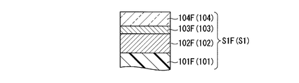
- Step 1 “Transparent conductive substrate S1F in which metal film 102F / intermediate film 103F / transparent conductive film 104F are sequentially laminated on transparent substrate 101F” is formed using a sputtering apparatus (for example, FIG. 5) described later. Then, the transparent conductive substrate S1F is carried out into the air atmosphere [FIG. 2A].
- Step 2 In order to perform batch patterning on the metal film 102F / intermediate film 103F / transparent conductive film 104F, a resist layer R patterned in a predetermined shape is formed on the surface of the transparent conductive film 104F [FIG. 2B].
- the transparent conductive substrate S1F on which the resist layer R is formed is also referred to as a processing object.
- Step 3 Etching solution EL is sprayed on the surface of the processing object S1m1 on which the resist layer R is formed, and the portion of the transparent conductive film 104F exposed from the resist layer R is etched [FIG. 2C].
- a solution capable of etching a structure composed of three layers metal film 102F / intermediate film 103F / transparent conductive film 104F
- three layers can be etched at once.
- a method of immersing the processing object S1m1 in the etching solution may be used.
- Step 4 After a predetermined time has elapsed, the etching is stopped [FIG. 2D]. Spraying on the processing object S1m2 is stopped or the processing object S1m2 is pulled up from the etching solution.
- FIG. 2D shows a case where etching is stopped. At this time, the transparent substrate 101m2 is exposed in the region where the resist layer is not disposed.
- Step 5 After cleaning the processing object S1m2 and removing the etching solution, the transparent conductive substrate S1E (S1) according to the embodiment of the present invention is obtained by removing the resist layer R.
- a mask having a desired void pattern (for example, a mesh pattern) is provided on the upper surface of the transparent conductive film 104, and three layers ( A step of etching the metal film 102F / intermediate film 103F / transparent conductive film 104F).
- the three layers metal film 102F / intermediate film 103F / transparent conductive film 104F
- the transparent conductive substrate S1 prepared in the above-described step 1 that is, “on the transparent substrate (glass substrate) 101, metal film (AlNd alloy film) 102F / intermediate film (MoNb oxide film) 103F / transparent conductive film.
- a method of manufacturing the “transparent conductive substrate S1F in which (ITO film) 104F is sequentially laminated” will be described.
- an interlock type sputtering apparatus as shown in FIG. 5 is used.
- the substrate 118 a (corresponding to the above-described base 101 made of a flexible member) is prepared by a transfer device (not shown) in a preparation / extraction chamber (L / UL) 111 and a heating chamber (H) 112.
- a transfer device not shown
- a preparation / extraction chamber L / UL
- H heating chamber
- the partition valves DV1 to DV7 are arranged between the adjacent chambers.
- a buffer chamber is arranged between the two film forming chambers.
- the manufacturing apparatus shown in FIG. 5 is configured such that an atmosphere of independent film formation conditions is maintained in first to third film formation spaces described later. However, when the first to third film formation spaces described later are not affected by other film formation spaces (for example, a desired differential pressure mechanism or the like is disposed in the film formation space), a partition valve or The manufacturing apparatus may have a single film formation space without providing the buffer chamber.
- the substrate 118a is transferred from the charging / unloading chamber 111 in a reduced-pressure atmosphere to the heating chamber 112 and subjected to a desired heat treatment.
- the substrate 118b is degassed and heated to a desired temperature. Further, depending on the material of the substrate to be used, heat treatment for degassing may be unnecessary.
- the substrate 118b after the heat treatment is transferred from the heating chamber 112 to the first film formation chamber 113, and passes through the front of the target 113TG made of a metal film base material (that is, the first film formation space sp1). Then, a metal film (AlNd alloy film) is formed on the substrate 118c. At this time, Ar gas is supplied from the process gas supply source 113G to the first film formation space sp1, and a desired pressure is maintained by the exhaust device 113P. If necessary, a temperature adjusting device (not shown) may be installed to control the temperature of the substrate 118c during film formation.
- Reference numeral 113BP represents a backing plate on which the target 113TG is placed, and reference numeral 113D represents a power source that supplies a high voltage to the backing plate 113BP.
- the substrate 118c on which the metal film is formed is transferred from the first film formation chamber 113 to the first buffer chamber 114.
- the first buffer chamber 114 is disposed between the first film formation chamber 113 (first film formation space sp1) and a second film formation chamber 115 (second film formation space sp2) described later, and is exhausted by an exhaust device 114P.
- a desired degree of vacuum is maintained in the internal space of the first buffer chamber 114.
- the substrate 118c on which the metal film is formed is transferred from the first buffer chamber 114 to the second film formation chamber 115, and before the target 115TG made of the base material of the intermediate film (that is, the second film formation space sp2). Then, an intermediate film (MoNb oxide film) is formed on the metal film (AlNd alloy film) of the substrate 118c. At that time, the (Ar + O 2 ) mixed gas is supplied from the process gas supply source 115G to the second film formation space sp2, and a desired pressure is maintained by the exhaust device 115P. If necessary, a temperature adjusting device (not shown) may be installed to control the temperature of the substrate 118c during film formation.
- Reference numeral 115BP represents a backing plate on which the target 115TG is placed, and reference numeral 115D represents a power source that supplies a high voltage to the backing plate 115BP.
- the substrate 118d having the intermediate film laminated on the metal film is transferred from the second film forming chamber 115 to the second buffer chamber 116.
- the second buffer chamber 116 is disposed between the second film formation chamber 115 (second film formation space sp2) and a third film formation chamber 117 (third film formation space sp3) described later, and is exhausted by an exhaust device 116P.
- a desired degree of vacuum is maintained in the internal space of the second buffer chamber 116.
- the substrate 118d in which the intermediate film is laminated on the metal film is transferred from the second buffer chamber 116 to the third film forming chamber 117, and before the target 117TG made of the base material of the transparent conductive film (that is, the third film By passing the film formation space sp3), a transparent conductive film (ITO) is formed on the intermediate film of the substrate 118d.
- the (Ar + O 2 ) mixed gas is supplied from the process gas supply source 117G to the third film formation space sp3, and a desired pressure is maintained by the exhaust device 117P.
- a temperature adjusting device (not shown) may be installed to control the temperature of the substrate 118d during film formation.
- Reference numeral 117BP represents a backing plate on which the target 117TG is placed, and reference numeral 117D represents a power source that supplies a high voltage to the backing plate 117BP.
- the substrate 118 on which the metal film, the intermediate film, and the transparent conductive film are sequentially formed is reversed (or reversely moved) as shown by an arrow RT in FIG. It is conveyed to the chamber 111 and taken out from the manufacturing apparatus to the outside (atmosphere). That is, the manufacturing apparatus shown in FIG. 5 has a first film formation space sp1 for forming the metal film, a second film formation space sp2 for forming the intermediate film, and a third film formation space for forming the transparent conductive film. At least sp3 is provided, and the second film formation space sp2 is disposed between the first film formation space sp1 and the third film formation space sp3 in the direction in which the substrate moves.
- a desired patterning is performed on the structure composed of three layers (metal film 102F / intermediate film 103F / transparent conductive film 104F) according to the embodiment of the present invention.
- a conductive substrate is obtained.
- Table 1 shows typical manufacturing conditions for the metal film, the intermediate film, and the transparent conductive film described above.
- Table 2 shows typical processing conditions of the etching process in the case of forming a three-layered mesh structure (FIGS. 1A to 1D and FIGS. 2A to 2D).
- a transparent conductive substrate provided with a structure composed of three mesh layers (metal film 102F / intermediate film 103F / transparent conductive film 104F) as shown in FIGS. 1A to 1D It can be produced stably.
- the apparatus for forming the metal film, the intermediate film, and the transparent conductive film as shown in Table 1 is not limited to the manufacturing apparatus shown in FIG. 5, for example, when a multi-chamber type manufacturing apparatus as shown in FIG. 6 is used. Even so, the transparent conductive substrate according to the embodiment of the present invention can be manufactured.
- FIG. 6 is a schematic view showing another example of the transparent conductive substrate manufacturing apparatus according to the embodiment of the present invention.
- the manufacturing apparatus shown in FIG. 6 corresponds to a case where each film forming step of the metal film, the intermediate film, and the transparent conductive film is performed in an independent film forming space chamber of a separate film forming chamber (chamber).
- the substrate is carried into the load chamber (L) 201 from the outside. Then, after the substrate waits for a certain time under reduced pressure in the load chamber, the substrate is transferred into the heating chamber (H) 202, and the substrate is subjected to heat treatment (degassing treatment) at a desired temperature.
- the heat-treated substrate is transferred from the heating chamber (H) 202 into the first film formation chamber (S1) 203, and a metal film is formed in the first film formation space sp1.
- the substrate on which the metal film is formed is transferred from the first film formation chamber (S1) 203 into the second film formation chamber (S2) 204, and an intermediate film is formed in the second film formation space sp2.
- the substrate on which the intermediate film is formed on the metal film is transferred from the second film formation chamber (S2) 204 into the third film formation chamber (S3) 205, and the transparent conductive film is formed in the third film formation space sp3. Film formation is performed.
- the substrate on which the intermediate film and the transparent conductive film are formed on the metal film is transferred from the third film formation chamber (S3) 205 to the unload chamber (UL) 206, and after waiting for a certain time, the unload chamber (UL) Unloaded from 206.
- a robot (not shown) installed in the transfer chamber (T) 207 is used as a device for transferring a substrate between the chambers. Note that the chambers 201 to 206 including the transfer chamber (T) 207 are all under reduced pressure during process processing and transfer in each chamber.
- the manufacturing apparatus shown in FIG. 6 includes a first film formation space sp1 for forming the metal film, a second film formation space sp2 for forming the intermediate film, and a third film formation space for forming the transparent conductive film. At least sp3 is provided, and the second film formation space sp2 is disposed between the first film formation space sp1 and the third film formation space sp3 in the direction in which the substrate moves.
- the present invention is not limited thereto.
- the transparent laminated structure may be provided on a member different from the transparent substrate of the above embodiment.
- the modification of embodiment of this invention is demonstrated. In the modification, the description about the member corresponding to the member in the above-described embodiment is omitted or simplified.
- FIG. 7A is a cross-sectional view schematically showing an example of a solar cell to which the above-described transparent laminated structure is applied.
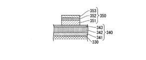
- FIG. 7B is an enlarged cross-sectional view schematically showing the structure of the transparent laminated structure in FIG. 7A.
- FIG. 9 is a cross-sectional view schematically showing an example of the structure of a conventional solar cell.
- a conventional solar cell 600 is provided on a single crystal silicon substrate 620 having a pn junction 630, a back electrode 610 provided on the back surface of the silicon substrate 620, and a surface of the silicon substrate 620.
- Finger electrode 640 and bus bar electrode 650 (bus bar wiring) provided on finger electrode 640 are provided.
- Bus bar electrode 650 collects electrons generated by power generation in silicon substrate 620.
- silver is used as a material for the bus bar electrode 650.
- the appearance color of the solar cell 600 (the color of the silicon substrate 620) is close to black, the contrast between the black color of the silicon substrate 620 and the silver white color of the bus bar electrode 650 is large, and the appearance is lacking in design. There was a problem.
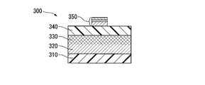
- a solar cell 300 according to the first modification includes a single crystal silicon substrate 320 having a pn junction 330, a back electrode 310 provided on the back surface of the silicon substrate 320, A finger electrode 340 provided on the surface of the silicon substrate 320 and a bus bar electrode 350 (bus bar wiring) provided on the finger electrode 340 and formed of a transparent laminated structure are provided. Further, the finger electrode 340 is provided on the pn junction 330, and an antireflection film is provided on the surface of the finger electrode 340. For this reason, the bus bar electrode 350 is provided on the antireflection film of the finger electrode 340.
- the bus bar electrode 350 includes a metal film 351 provided on the finger electrode 340, an intermediate film 352 provided on the metal film 351, and a transparent conductive film 353 provided on the intermediate film 352. With. That is, the intermediate film 352 is sandwiched between the metal film 351 and the transparent conductive film 353. The conductivity of the bus bar electrode 350 is obtained by the metal film 351.
- the intermediate film 352 is an oxide film containing molybdenum.
- the transparent laminated structure is applied to the bus bar electrode 350, so that the reflected light from the bus bar electrode is reduced. be able to. Therefore, the problem that the contrast between the silver white color of the bus bar electrode 650 and the black color of the silicon substrate 620 in the conventional solar cell 600 is solved.
- FIG. 7C is an enlarged cross-sectional view showing a finger electrode constituted by a transparent laminated structure.
- the finger electrode 340 includes a metal film 341 provided on the pn junction 330, an intermediate film 342 provided on the metal film 341, and a transparent conductive film provided on the intermediate film 342. 343. That is, the intermediate film 342 is sandwiched between the metal film 341 and the transparent conductive film 343.
- the finger electrode 340 having such a transparent laminated structure, in order to obtain conductivity between the finger electrode 340 and the bus bar electrode 350, a part of the finger electrode 340 (intermediate film 342 and transparent conductive film 343) is formed.
- the finger electrode 340 and the bus bar electrode 350 may be electrically connected by being partially removed.
- the solar cell 300 according to the second modification not only the effects in the above-described embodiment can be obtained, but also the finger electrode 340 is applied with the transparent laminated structure, so that the reflected light from the finger electrode is reduced. can do.
- the base material may be a transparent base material or a colored base material.
- a low reflection structure can be implement
- the transparent laminated structure has a metal film, conductivity is obtained, and charging of components constituting the internal mechanism of the optical system apparatus can be prevented.
- the present invention is widely applicable to transparent conductive substrates.
- the transparent conductive substrate of the present invention is suitably used for a high-quality display screen that requires excellent visibility.
- S1 (S1E, S1F) transparent conductive substrate 101 (101E, 101F) substrate (transparent substrate), 101ET substrate surface, 102 (102E, 102F) metal film, 103 (103E, 103F) intermediate film, 104 (104E, 104F) Surface of transparent conductive film, 104ET transparent conductive film.
Landscapes
- Engineering & Computer Science (AREA)
- General Engineering & Computer Science (AREA)
- Theoretical Computer Science (AREA)
- Human Computer Interaction (AREA)
- Physics & Mathematics (AREA)
- General Physics & Mathematics (AREA)
- Laminated Bodies (AREA)
- Non-Insulated Conductors (AREA)
- Physical Vapour Deposition (AREA)
Abstract
Description
本願は、2015年3月25日に日本に出願された特願2015-062735号に基づき優先権を主張し、その内容をここに援用する。
それゆえ、安定した導電性を得るとともに、反射光が観察者に認識されることを抑制し、さらにFPCとセンサー電極とを容易に電気的に接続することが可能な、メタルメッシュ構造を備えた透明導電性基板の開発が期待されていた。
本発明の第二態様に係る透明導電性基板は、透明基体と、前記透明基体の一面に、金属膜、モリブデン(Mo)を含む酸化膜である中間膜、及び透明導電膜が順に積層された構造体とを備える。前記構造体においては、波長550nmの入射光に対して反射率が5[%]以下である。
本発明の第一態様及び第二態様に係る透明導電性基板においては、前記中間膜の比抵抗[μΩ・cm]が1.8×10⁸以下であってもよい。
本発明の第一態様及び第二態様に係る透明導電性基板においては、前記透明導電膜の膜厚[nm]が10以上50以下の範囲であってもよい。
本発明の第一態様及び第二態様に係る透明導電性基板においては、前記中間膜の比抵抗及び前記透明導電膜の膜厚のうち少なくとも一つを制御することにより、前記構造体の色合いが調整可能であってもよい。
本発明の第一態様及び第二態様に係る透明導電性基板においては、前記透明基体の前記一面において、前記金属膜、前記中間膜、前記透明導電膜が順に積層されてなる構造体が、エッチング処理により所望のパターンを有してもよい。
本発明の第三態様に係る透明積層構造体は、金属膜と、前記金属膜上に設けられ、モリブデン(Mo)を含む酸化膜である中間膜と、前記中間膜上に設けられた透明導電膜とを備える。前記透明積層構造体においては、可視光域の入射光に対して平均反射率が10[%]以下である。
ここで、可視光域(波長域が380~780[nm])の入射光に対して平均反射率が10[%]以下の条件、もしくは、特に人の目を通じて最も明るく視認される550nmの波長において反射率が5[%]以下の条件を満たすことにより、前記構造体は低反射構造をとるようになり、所望の色合いに調整することができるようになるとともに、電極としての導電性も確保される。特に、前記構造体においては、中間膜に含まれる酸素量と、透明導電膜の厚さとを制御することにより、構造体の低抵抗化と高い透過率とを両立することができる。
ゆえに、本発明の上記態様は、安定した導電性を得るともに、反射光が観察者に認識されることを抑制するメタルメッシュ構造を備えた透明導電性基板の提供に貢献する。
図1A~図1Dは、本実施形態における透明導電性基板を示す模式図であり、図1Aは全体平面図であり、図1Bは領域P1の拡大平面図であり、図1C及び図1Dは図1Bの線A-Aの断面図を表している。特に、図1Cは、エッチング後の透明導電性基板を示す断面図であり、図1Dは、エッチング前の透明導電性基板を示す断面図である。
このような透明導電性基板S1E(S1)は、図1A~図1Dに示すように、ガラス等からなる絶縁性の透明基体101E(101)の一面101ETに、金属膜102E(102)、中間膜103E(103)、透明導電膜104E(104)が順に積層されてなる構造体(透明積層構造体)を備えている。
このような条件を満たす金属膜の部材としては、例えば、Al、Al合金、Mo、Mo合金、Ti、Ti合金、Cu、Cu合金、等が挙げられる。中でも、Alにネオジム(Nd)を含有させた(Al-Nd)合金からなる金属膜が、安定した導電性、耐候性を得られるという点から好ましく、さらに、Ndの添加によりAlに特有の問題であるヒロックの発生を抑制することも可能であるため好ましい。
図3において、横軸は入射光の波長を表しており、縦軸は反射率を表わしている。図3における実線は、本発明の実施形態に係る3層の積層構造を有する実施例の透明積層構造体の結果を示している。図3における点線は、比較例の透明導電性基板の結果を示している。
比較例の透明導電性基板は、実施例の3層構造を有する透明導電性基板とは異なり、中間膜と透明導電膜が設けられていない構成、すなわち、基体の上に金属膜のみが形成された透明導電性基板である。
(1)中間膜に含まれる酸素量を調整することにより、中間膜の色合いを制御することが可能である。
(2)特に、中間膜103の比抵抗を1.8×10⁸[μΩ・cm]以下とした場合には、低反射構造を得ることができ、かつ、その範囲内で中間膜の色合いを制御できる。
(3)具体的には、比抵抗が下がるにつれて、着色の度合いを増加させることが可能となる。換言すると、比抵抗が下がるにつれて、中間膜の色合いが濃くなる現象が確認された。
このような透明導電膜の膜厚としては、金属膜や中間膜の膜厚、材質等にもよるが、導電性を確保しつつ、下層(透明導電膜の下方に位置する層)と、透明導電膜との間の光学的な調整が可能となる範囲として、10~50nmが好ましい。
以下では、上述した工程1で用意した透明導電性基板S1、すなわち、「透明基体(ガラス基板)101上に、金属膜(AlNd合金膜)102F/中間膜(MoNb酸化膜)103F/透明導電膜(ITO膜)104Fが順に積層されてなる」透明導電性基板S1F、の作製方法について説明する。
つまり、図5に示す製造装置は、前記金属膜を形成する第一成膜空間sp1、前記中間膜を形成する第二成膜空間sp2、及び、前記透明導電膜を形成する第三成膜空間sp3を少なくとも備えており、前記基体が移動する方向において、前記第二成膜空間sp2が、前記第一成膜空間sp1と前記第三成膜空間sp3との間に配置されている。
上述した金属膜と中間膜と透明導電膜の代表的な作製条件を表1に示す。また、メッシュ状の3層からなる構造体を形成する場合(図1A~図1D及び図2A~図2D)の代表的なエッチング工程の処理条件を表2に示す。

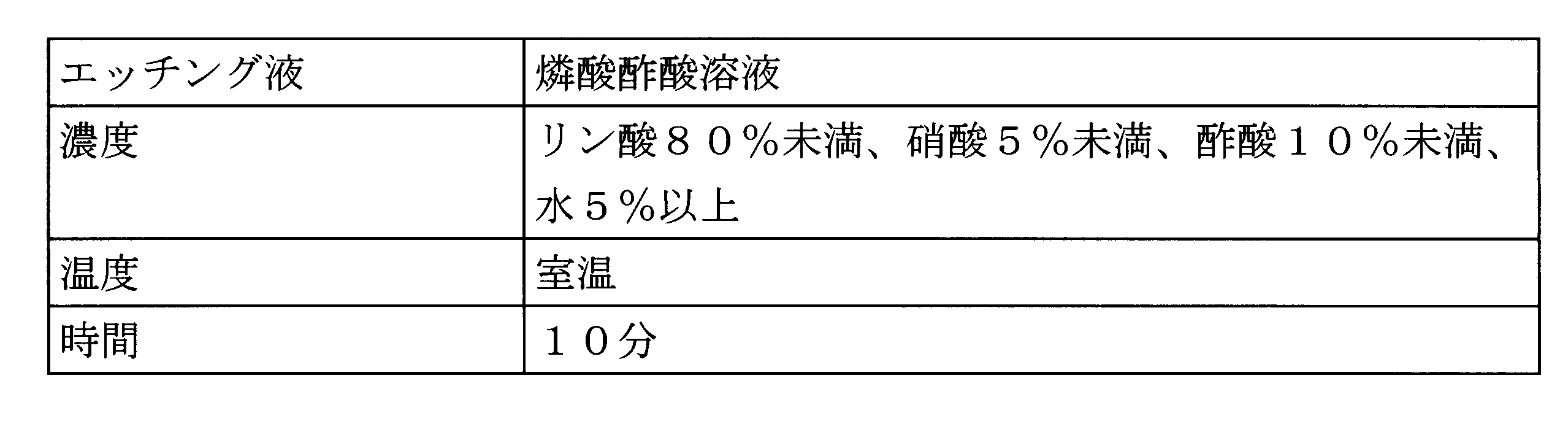
表1に示すような、金属膜と中間膜と透明導電膜を作成する装置は、図5に示す製造装置に限定されず、例えば、図6に示すようなマルチチャンバ型の製造装置を用いる場合であっても、本発明の実施形態に係る透明導電性基板を製造することができる。
以下に、本発明の実施形態の変形例について説明する。変形例においては、上述した実施形態における部材に相当する部材に関する説明を省略または簡略化する。
図7Aは、上述した透明積層構造体が適用された太陽電池の一例を模式的に示す断面図である。図7Bは、図7Aにおける透明積層構造体の構造を模式的に示す拡大断面図である。図9は、従来の太陽電池の構造の一例を模式的に示す断面図である。
図9に示すように従来の太陽電池600は、pn接合部630を有する単結晶のシリコン基板620と、シリコン基板620の裏面に設けられた裏面電極610と、シリコン基板620の表面に設けられたフィンガー電極640と、フィンガー電極640上に設けられたバスバー電極650(バスバー配線)とを備える。
バスバー電極650は、シリコン基板620における発電によって生成された電子を集電する。また、一般的に、バスバー電極650の材料としては、銀が利用されている。しかしながら、太陽電池600の外観色(シリコン基板620の色)は黒色に近い色であるため、シリコン基板620の黒色とバスバー電極650の銀白色とのコントラストが大きく、外観上、デザイン性に欠けるという問題があった。
具体的に、図7Aに示すように、本変形例1に係る太陽電池300は、pn接合部330を有する単結晶のシリコン基板320と、シリコン基板320の裏面に設けられた裏面電極310と、シリコン基板320の表面に設けられたフィンガー電極340と、フィンガー電極340上に設けられて透明積層構造体で構成されたバスバー電極350(バスバー配線)とを備える。また、フィンガー電極340は、pn接合部330上に設けられており、フィンガー電極340の表面には、反射防止膜が設けられている。このため、フィンガー電極340の反射防止膜上にバスバー電極350が設けられている。
金属膜351によってバスバー電極350の導電性が得られている。中間膜352は、モリブデンを含む酸化膜である。透明導電膜353の酸化度や膜厚を調整することで、低反射率を有する透明積層構造体で構成されたバスバー電極350が実現されている。
図7Cは、透明積層構造体によって構成されたフィンガー電極を示す拡大断面図である。変形例2においては、変形例1と同一部材には同一符号を付して、その説明は省略または簡略化する。
図7Cに示すように、フィンガー電極340は、pn接合部330上に設けられた金属膜341と、金属膜341上に設けられた中間膜342と、中間膜342上に設けられた透明導電膜343とを備える。即ち、中間膜342が金属膜341と透明導電膜343の間に挟持されている。
このような透明積層構造体を備えるフィンガー電極340においては、フィンガー電極340とバスバー電極350との間において導電性を得るために、フィンガー電極340の一部(中間膜342、透明導電膜343)を部分的に除去し、フィンガー電極340とバスバー電極350とを電気的に接続してもよい。
本変形例2に係る太陽電池300によれば、上述した実施形態における効果が得られるだけでなく、フィンガー電極340にも透明積層構造体が適用されているので、フィンガー電極からの反射光を低減することができる。
上述した透明積層構造体を光学系機器用の遮光フィルムに適用してもよい。
一般的に、デジタルカメラ等のデジタル光学系機器においては、光学系機器の内部機構を構成する部材の表面に低反射性、導電性に優れた機能膜を形成することが知られている(例えば、特開2008-281977等)。
このような機能膜として、上述した実施形態に係る透明積層構造体を適用してもよい。この場合、樹脂フィルム等の基材の表面及び裏面の両方に透明積層構造体が形成される。また、シャッター羽根や絞り羽根等に加工された部材の表面に透明積層構造体を直接形成してもよい。また、光学系機器を構成する部材の表面全体が低反射構造を有する必要があることから、光学系機器を構成する部材の表面全体に上述した透明積層構造体を形成すればよい。この場合、基材は、透明基材であってもよいし、着色された基材であってもよい。
また、本変形例3における透明積層構造体においては、中間膜及び透明導電膜の酸化度や膜厚を制御することで、低反射構造体を実現することができる。また、透明積層構造体が金属膜を有することため、導電性が得られており、光学系機器の内部機構を構成する部品の帯電を予防することもできる。
Claims (7)
- 透明導電性基板であって、
透明基体と、
前記透明基体の一面に、金属膜、モリブデン(Mo)を含む酸化膜である中間膜、及び透明導電膜が順に積層された構造体と
を備え、
前記構造体においては、可視光域の入射光に対して平均反射率が10[%]以下である透明導電性基板。 - 透明導電性基板であって、
透明基体と、
前記透明基体の一面に、金属膜、モリブデン(Mo)を含む酸化膜である中間膜、及び透明導電膜が順に積層された構造体と
を備え、
前記構造体においては、波長550nmの入射光に対して反射率が5[%]以下である請求項1に記載の透明導電性基板。 - 前記中間膜の比抵抗[μΩ・cm]が1.8×10⁸以下である請求項1又は請求項2に記載の透明導電性基板。
- 前記透明導電膜の膜厚[nm]が10以上50以下の範囲である請求項1から請求項3のいずれか一項に記載の透明導電性基板。
- 前記中間膜の比抵抗及び前記透明導電膜の膜厚のうち少なくとも一つを制御することにより、前記構造体の色合いが調整可能である請求項1から請求項4のいずれか一項に記載の透明導電性基板。
- 前記透明基体の前記一面において、前記金属膜、前記中間膜、前記透明導電膜が順に積層されてなる構造体が、エッチング処理により所望のパターンを有している請求項1から請求項5のいずれか一項に記載の透明導電性基板。
- 透明積層構造体であって、
金属膜と、
前記金属膜上に設けられ、モリブデン(Mo)を含む酸化膜である中間膜と、
前記中間膜上に設けられた透明導電膜と
を備え、
前記透明積層構造体においては、可視光域の入射光に対して平均反射率が10[%]以下である透明積層構造体。
Priority Applications (3)
| Application Number | Priority Date | Filing Date | Title |
|---|---|---|---|
| JP2017508222A JP6494001B2 (ja) | 2015-03-25 | 2016-03-11 | 透明導電性基板及び透明積層構造体 |
| KR1020177022063A KR101941394B1 (ko) | 2015-03-25 | 2016-03-11 | 투명 도전성 기판 및 투명 적층 구조체 |
| CN201680010302.4A CN107250959B (zh) | 2015-03-25 | 2016-03-11 | 透明导电性基板及透明层叠结构体 |
Applications Claiming Priority (2)
| Application Number | Priority Date | Filing Date | Title |
|---|---|---|---|
| JP2015-062735 | 2015-03-25 | ||
| JP2015062735 | 2015-03-25 |
Publications (1)
| Publication Number | Publication Date |
|---|---|
| WO2016152581A1 true WO2016152581A1 (ja) | 2016-09-29 |
Family
ID=56979263
Family Applications (1)
| Application Number | Title | Priority Date | Filing Date |
|---|---|---|---|
| PCT/JP2016/057770 Ceased WO2016152581A1 (ja) | 2015-03-25 | 2016-03-11 | 透明導電性基板及び透明積層構造体 |
Country Status (5)
| Country | Link |
|---|---|
| JP (1) | JP6494001B2 (ja) |
| KR (1) | KR101941394B1 (ja) |
| CN (1) | CN107250959B (ja) |
| TW (1) | TW201706799A (ja) |
| WO (1) | WO2016152581A1 (ja) |
Cited By (2)
| Publication number | Priority date | Publication date | Assignee | Title |
|---|---|---|---|---|
| CN109153606A (zh) * | 2016-10-12 | 2019-01-04 | 积水化学工业株式会社 | 夹层玻璃用中间膜、卷体以及夹层玻璃 |
| US10847076B2 (en) | 2018-04-26 | 2020-11-24 | Samsung Display Co., Ltd. | Wiring substrate, display device including the wiring substrate, and method of fabricating the wiring substrate |
Citations (3)
| Publication number | Priority date | Publication date | Assignee | Title |
|---|---|---|---|---|
| JPH06247716A (ja) * | 1992-12-28 | 1994-09-06 | Mitsubishi Materials Corp | 低抵抗導電性顔料及びその製造方法 |
| JPH10241464A (ja) * | 1996-12-26 | 1998-09-11 | Asahi Glass Co Ltd | 透明導電膜付き基体とその製造方法 |
| EP2767985A1 (en) * | 2012-08-31 | 2014-08-20 | LG Chem, Ltd. | Conductive structure and method for manufacturing same |
Family Cites Families (7)
| Publication number | Priority date | Publication date | Assignee | Title |
|---|---|---|---|---|
| KR100738212B1 (ko) | 2004-11-11 | 2007-07-12 | 엘지전자 주식회사 | 플라즈마 디스플레이 패널 |
| TWI432115B (zh) * | 2010-10-19 | 2014-03-21 | Lg Chemical Ltd | 包含導電圖案之觸控面板及其製備方法 |
| CN103197781A (zh) * | 2012-01-04 | 2013-07-10 | 北儒精密股份有限公司 | 低色差触控基板及其制造方法 |
| JP2013206315A (ja) | 2012-03-29 | 2013-10-07 | Toppan Printing Co Ltd | フィルム状タッチパネルセンサー及びその製造方法 |
| CN104345932B (zh) * | 2013-07-29 | 2017-07-14 | 和鑫光电股份有限公司 | 触控面板 |
| KR20150107337A (ko) * | 2014-03-14 | 2015-09-23 | 삼성전기주식회사 | 터치 감지 방법 및 터치스크린 장치 |
| CN104020880A (zh) * | 2014-05-27 | 2014-09-03 | 京东方科技集团股份有限公司 | 一种触摸显示装置 |
-
2016
- 2016-03-11 JP JP2017508222A patent/JP6494001B2/ja active Active
- 2016-03-11 KR KR1020177022063A patent/KR101941394B1/ko active Active
- 2016-03-11 CN CN201680010302.4A patent/CN107250959B/zh active Active
- 2016-03-11 WO PCT/JP2016/057770 patent/WO2016152581A1/ja not_active Ceased
- 2016-03-23 TW TW105109063A patent/TW201706799A/zh unknown
Patent Citations (3)
| Publication number | Priority date | Publication date | Assignee | Title |
|---|---|---|---|---|
| JPH06247716A (ja) * | 1992-12-28 | 1994-09-06 | Mitsubishi Materials Corp | 低抵抗導電性顔料及びその製造方法 |
| JPH10241464A (ja) * | 1996-12-26 | 1998-09-11 | Asahi Glass Co Ltd | 透明導電膜付き基体とその製造方法 |
| EP2767985A1 (en) * | 2012-08-31 | 2014-08-20 | LG Chem, Ltd. | Conductive structure and method for manufacturing same |
Cited By (2)
| Publication number | Priority date | Publication date | Assignee | Title |
|---|---|---|---|---|
| CN109153606A (zh) * | 2016-10-12 | 2019-01-04 | 积水化学工业株式会社 | 夹层玻璃用中间膜、卷体以及夹层玻璃 |
| US10847076B2 (en) | 2018-04-26 | 2020-11-24 | Samsung Display Co., Ltd. | Wiring substrate, display device including the wiring substrate, and method of fabricating the wiring substrate |
Also Published As
| Publication number | Publication date |
|---|---|
| CN107250959A (zh) | 2017-10-13 |
| TW201706799A (zh) | 2017-02-16 |
| JP6494001B2 (ja) | 2019-04-03 |
| CN107250959B (zh) | 2021-02-05 |
| JPWO2016152581A1 (ja) | 2017-09-28 |
| KR101941394B1 (ko) | 2019-01-22 |
| KR20170104542A (ko) | 2017-09-15 |
Similar Documents
| Publication | Publication Date | Title |
|---|---|---|
| CN104303240B (zh) | 带有透明电极的基板及其制造方法以及触摸面板 | |
| KR101648636B1 (ko) | 전도성 구조체 및 이의 제조방법 | |
| US20170168616A1 (en) | Substrate, touch display panel having the same, and method thereof | |
| US10026523B2 (en) | Conductor and method of manufacturing the same | |
| US20140349070A1 (en) | Reflective anode electrode for use in an organic electroluminescent display and method for making the same | |
| KR102388000B1 (ko) | 광 투과성 필름 | |
| JP2011175900A (ja) | 透明導電性積層体及びその製造方法 | |
| US10528167B2 (en) | Conductive structure, method for manufacturing same, touch panel comprising same and display device comprising same | |
| KR101847751B1 (ko) | 입력 장치에 사용되는 전극, 및 그 제조 방법 | |
| JP6292225B2 (ja) | 透明導電体 | |
| JP6494001B2 (ja) | 透明導電性基板及び透明積層構造体 | |
| JPWO2014171149A1 (ja) | 透明導電体及びその製造方法 | |
| WO2016158181A1 (ja) | 窒素含有Cu合金膜、積層膜、およびこれらの製造方法、ならびにCu合金スパッタリングターゲット | |
| CN111240507A (zh) | 导电性薄膜和其图案化方法 | |
| JP2007163995A (ja) | 透明導電膜付き基板およびその製造方法 | |
| JP6497744B2 (ja) | タッチパネル | |
| JP7326918B2 (ja) | 積層体 | |
| JP2016177940A (ja) | 透明導電体の製造方法 | |
| WO2015125677A1 (ja) | 透明導電体 | |
| WO2015190227A1 (ja) | 透明導電体の製造方法 | |
| KR20160019303A (ko) | 알루미늄 패턴 및 이의 제조 방법 | |
| WO2016171097A1 (ja) | 透明導電性基板及びその製造方法、並びに、透明導電性基板の製造装置 | |
| CN106255945A (zh) | 触摸面板、触摸面板的制造方法以及光学薄膜 | |
| JP2018170360A (ja) | 導電膜,電極,電子機器,静電容量型入力装置及び電極の製造方法 | |
| KR20160088695A (ko) | 전도성 구조체 및 이의 제조방법 |
Legal Events
| Date | Code | Title | Description |
|---|---|---|---|
| 121 | Ep: the epo has been informed by wipo that ep was designated in this application |
Ref document number: 16768484 Country of ref document: EP Kind code of ref document: A1 |
|
| ENP | Entry into the national phase |
Ref document number: 2017508222 Country of ref document: JP Kind code of ref document: A |
|
| ENP | Entry into the national phase |
Ref document number: 20177022063 Country of ref document: KR Kind code of ref document: A |
|
| NENP | Non-entry into the national phase |
Ref country code: DE |
|
| 122 | Ep: pct application non-entry in european phase |
Ref document number: 16768484 Country of ref document: EP Kind code of ref document: A1 |