WO2016158181A1 - 窒素含有Cu合金膜、積層膜、およびこれらの製造方法、ならびにCu合金スパッタリングターゲット - Google Patents
窒素含有Cu合金膜、積層膜、およびこれらの製造方法、ならびにCu合金スパッタリングターゲット Download PDFInfo
- Publication number
- WO2016158181A1 WO2016158181A1 PCT/JP2016/056491 JP2016056491W WO2016158181A1 WO 2016158181 A1 WO2016158181 A1 WO 2016158181A1 JP 2016056491 W JP2016056491 W JP 2016056491W WO 2016158181 A1 WO2016158181 A1 WO 2016158181A1
- Authority
- WO
- WIPO (PCT)
- Prior art keywords
- layer
- film
- less
- alloy
- laminated film
- Prior art date
- Legal status (The legal status is an assumption and is not a legal conclusion. Google has not performed a legal analysis and makes no representation as to the accuracy of the status listed.)
- Ceased
Links
Images


Classifications
-
- B—PERFORMING OPERATIONS; TRANSPORTING
- B32—LAYERED PRODUCTS
- B32B—LAYERED PRODUCTS, i.e. PRODUCTS BUILT-UP OF STRATA OF FLAT OR NON-FLAT, e.g. CELLULAR OR HONEYCOMB, FORM
- B32B15/00—Layered products comprising a layer of metal
- B32B15/01—Layered products comprising a layer of metal all layers being exclusively metallic
-
- C—CHEMISTRY; METALLURGY
- C23—COATING METALLIC MATERIAL; COATING MATERIAL WITH METALLIC MATERIAL; CHEMICAL SURFACE TREATMENT; DIFFUSION TREATMENT OF METALLIC MATERIAL; COATING BY VACUUM EVAPORATION, BY SPUTTERING, BY ION IMPLANTATION OR BY CHEMICAL VAPOUR DEPOSITION, IN GENERAL; INHIBITING CORROSION OF METALLIC MATERIAL OR INCRUSTATION IN GENERAL
- C23C—COATING METALLIC MATERIAL; COATING MATERIAL WITH METALLIC MATERIAL; SURFACE TREATMENT OF METALLIC MATERIAL BY DIFFUSION INTO THE SURFACE, BY CHEMICAL CONVERSION OR SUBSTITUTION; COATING BY VACUUM EVAPORATION, BY SPUTTERING, BY ION IMPLANTATION OR BY CHEMICAL VAPOUR DEPOSITION, IN GENERAL
- C23C14/00—Coating by vacuum evaporation, by sputtering or by ion implantation of the coating forming material
- C23C14/06—Coating by vacuum evaporation, by sputtering or by ion implantation of the coating forming material characterised by the coating material
- C23C14/14—Metallic material, boron or silicon
-
- C—CHEMISTRY; METALLURGY
- C23—COATING METALLIC MATERIAL; COATING MATERIAL WITH METALLIC MATERIAL; CHEMICAL SURFACE TREATMENT; DIFFUSION TREATMENT OF METALLIC MATERIAL; COATING BY VACUUM EVAPORATION, BY SPUTTERING, BY ION IMPLANTATION OR BY CHEMICAL VAPOUR DEPOSITION, IN GENERAL; INHIBITING CORROSION OF METALLIC MATERIAL OR INCRUSTATION IN GENERAL
- C23C—COATING METALLIC MATERIAL; COATING MATERIAL WITH METALLIC MATERIAL; SURFACE TREATMENT OF METALLIC MATERIAL BY DIFFUSION INTO THE SURFACE, BY CHEMICAL CONVERSION OR SUBSTITUTION; COATING BY VACUUM EVAPORATION, BY SPUTTERING, BY ION IMPLANTATION OR BY CHEMICAL VAPOUR DEPOSITION, IN GENERAL
- C23C14/00—Coating by vacuum evaporation, by sputtering or by ion implantation of the coating forming material
- C23C14/22—Coating by vacuum evaporation, by sputtering or by ion implantation of the coating forming material characterised by the process of coating
- C23C14/34—Sputtering
Definitions
- the present invention relates to a nitrogen-containing Cu alloy film, a laminated film, a manufacturing method thereof, and a Cu alloy sputtering target.
- Metal material shows high conductivity but high reflectivity. Therefore, for example, metal mesh wiring has been proposed in which a metal thin film capable of realizing a resistance lower than that of an ITO thin film is processed into a mesh shape on a sensor electrode of a touch panel.
- the metal thin film has a high reflectance as described above, there is a problem that the mesh pattern of the wiring is visualized. Therefore, when a metal thin film is used for the electrode, it is required to suppress reflection from the metal thin film.
- the suppression of the reflection from the metal thin film may be hereinafter referred to as “improvement of visibility”.
- improved visibility As an electrode structure with improved visibility, for example, the techniques of Patent Documents 1 to 3 listed below can be cited.
- Patent Document 1 a plurality of conductive pattern cells spaced from each other are formed on a substrate, an insulating layer is formed on the conductive pattern cell, and a black conductive material is used on the insulating layer.
- a method of manufacturing an electrode pattern for a touch panel is described, which is characterized by forming a bridge electrode for interconnecting conductive pattern cells.
- the bridge electrode uses Al, Au, Ag, Sn, Cr, Ni, Ti, or Mg metal, and is shown to be blackened by oxidation, nitridation, and fluorination by reaction with chemicals.
- Patent Document 1 discloses a technique for reducing the reflectance of a bridge electrode by blackening a metal, but does not consider any reduction in electrical resistivity. For this reason, in the above technique, the resistance of the electrode may be increased by the metal oxide, which is not suitable for the electrode.
- Patent Document 1 includes metals that are highly reactive and difficult to handle, such as Ag nitride and Mg oxide, or that are difficult to finely process. It is.
- Patent Document 2 discloses a transparent conductive film that does not cause misalignment of the two films even in a mesh form without reducing the visibility of the display disposed under the touch panel due to the metallic gloss reflection light of the wiring portion.
- a laminate that can be applied to is shown.
- As the laminate a laminate having at least two blackening layers and one substrate is shown. Further, as the blackening layer, a layer including at least one selected from the group consisting of copper nitride, copper oxide, nickel nitride, and nickel oxide is shown.
- the blackened layer is preferably a layer having a total content of copper and nickel (based on the number of atoms) of 50 atomic% or more and 95 atomic% or less, and a total content of nitrogen and oxygen in 100 atomic% of the whole layer. It is indicated that the layer is (atomic number basis) of 5 atomic% or more and 50 atomic% or less.
- Patent Document 3 discloses a laminate that can be applied to a transparent conductive film in which the color tone of blackening does not change over time, and the visibility of a display disposed under a touch panel does not deteriorate. It is shown.
- the laminated body has a copper nitride in the blackened layer when the total number of nitrogen atoms constituting the oxide of copper nitride and nitrogen atoms constituting the non-oxide of copper nitride is 100 atomic%. It is shown that the number of nitrogen atoms constituting the copper nitride oxide is 1 atomic% or more and 50 atomic% or less.
- the present invention has been made by paying attention to the circumstances as described above, and the object thereof is to provide a low-reflection conductive film or a high-conductivity low-reflection conductive film that exhibits high conductivity and suppresses reflection from a metal thin film and improves visibility.
- An object of the present invention is to provide a laminated film useful as a low reflection wiring.
- Another object of the present invention is to provide a nitrogen-containing Cu alloy film as a single layer film having a high light absorption rate in the visible light region and useful as a light absorption film, and having excellent wiring processability. To do. Furthermore, the present invention provides a laminated film useful as a low-reflective conductive film or low-reflective wiring having the nitrogen-containing Cu alloy film, showing high conductivity, improved visibility, and excellent wiring processability. Also aimed.
- the nitrogen-containing Cu alloy film of the present invention that has solved the above problems contains at least one X element selected from Ni and Al, the balance is Cu and inevitable impurities, and a part of the film is nitrided,
- the film thickness is 50 nm
- the reflectance at a wavelength of 650 nm is 45% or less
- the light absorptance at a wavelength of 650 nm is 40% or more.
- the laminated film of the present invention that can solve the above-mentioned problems is made of Ag, Al, Cu, or an alloy based on these as the first layer and has an electric resistivity of 1.0 ⁇ 10 ⁇ .
- the visible light reflectance of the two-layer laminated film of the first layer and the second layer is 45% or less, and the sheet resistance of the two-layer laminated film is 1.0 ⁇ / ⁇ or less.
- the visible light reflectance refers to reflectances of all wavelengths of wavelengths 450 nm, 550 nm, and 650 nm, as shown in examples described later. The same applies hereinafter.
- Another laminated film of the present invention that has solved the above-mentioned problems is made of Ag, Al, Cu, or an alloy based on these as the first layer and has an electrical resistivity of 1.0 ⁇ .
- the three-layer laminated film of the third layer and the third layer is characterized in that the visible light reflectance is 30% or less, and the sheet resistance of the three-layer laminated film is 1.0 ⁇ / ⁇ or less.
- another laminated film of the present invention that has solved the above-mentioned problems is made of Ag, Al, Cu, or an alloy based on these as the first layer and has an electrical resistivity of 1.0 ⁇ . It has a film that is 10 ⁇ 5 ⁇ ⁇ cm or less and the nitrogen-containing Cu alloy film as the second layer, and the visible light reflectance of the two-layer laminated film of the first layer and the second layer is 45% or less. And the sheet resistance of the two-layer laminated film is 1.0 ⁇ / ⁇ or less.
- another laminated film of the present invention that has solved the above-mentioned problems is made of Ag, Al, Cu, or an alloy based on these as the first layer and has an electrical resistivity of 1.0 ⁇ . 10 ⁇ 5 ⁇ ⁇ cm or less, as the second layer, the nitrogen-containing Cu alloy film, and as the third layer, at least one element selected from the group consisting of In, Zn, Sn and Al.
- the visible light reflectance of the three-layer laminated film of the first layer, the second layer, and the third layer is 30% or less, and the sheet resistance of the three-layer laminated film is 1 It is characterized in that it is 0.0 ⁇ / ⁇ or less.
- the first layer is preferably a Cu alloy film containing at least one Z element selected from the group consisting of Mn, Ni, Co, Ge, Zn and Ti.
- the third layer is preferably an oxide film containing at least In.
- the thickness of the first layer is preferably 40 to 400 nm.
- the present invention may include a low-reflection conductive film or low-reflection wiring having the nitrogen-containing Cu alloy film, or a low-reflection conductive film or low-reflection wiring having the laminated film.
- the present invention also includes a display device, a touch panel sensor, and an electromagnetic wave shield that can include the nitrogen-containing Cu alloy film or the laminated film as, for example, the low-reflection conductive film or the low-reflection wiring.
- the present invention includes a Cu alloy sputtering target for forming the nitrogen-containing Cu alloy film.
- the present invention further includes a method for producing the nitrogen-containing Cu alloy film or laminated film.
- This method is characterized in that the nitrogen-containing Cu alloy film or a Cu film in which a part of the film is nitrided is formed by reactive sputtering in an atmosphere containing nitrogen gas or nitrogen-containing gas.
- a laminated film useful as a low-reflection conductive film or low-reflection wiring that exhibits high conductivity and improved visibility.
- a nitrogen-containing Cu alloy film can be provided as a single layer film having a high light absorption rate in the visible light region, useful as a light absorption film, and excellent in wiring processability.
- a low-reflective conductive film or a laminated film useful as a low-reflective wiring which has the nitrogen-containing Cu alloy film, exhibits high conductivity, has improved visibility, and has excellent wiring processability.
- the laminated film of the present invention is excellent in wiring processability as described above, even when an etching solution containing iron chloride is used by a wet etching method, a good wiring shape, for example, a submicron pattern has been obtained. Wiring can be obtained.
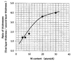
- FIG. 1 is a diagram showing the relationship between the amount of added Ni and the ratio of film thickness when the side etching width is 5.0 ⁇ m in wiring processing of a two-layer laminated film composed of a Cu—Ni—N thin film and a Cu thin film. It is.
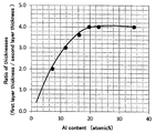
- FIG. 2 is a diagram showing the relationship between the Al addition amount and the film thickness ratio when the side etching width is 5.0 ⁇ m in the wiring processing of the two-layer laminated film composed of the Cu—Al—N thin film and the Cu thin film. It is.
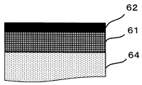
- FIG. 3 is a schematic cross-sectional view showing a structural example of the laminated film of the present invention.
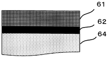
- FIG. 4 is a schematic sectional view showing another structural example of the laminated film of the present invention.
- FIG. 1 is a diagram showing the relationship between the amount of added Ni and the ratio of film thickness when the side etching width is 5.0 ⁇ m in wiring processing of a two-layer laminated film composed of a Cu—Ni—N thin film and
- FIG. 5 is a schematic sectional view showing another structural example of the laminated film of the present invention.
- FIG. 6 is a schematic sectional view showing another structural example of the laminated film of the present invention.
- FIG. 7 is a schematic sectional view showing another structural example of the laminated film of the present invention.
- FIG. 8 is a schematic sectional view showing another structural example of the laminated film of the present invention.
- FIG. 9 is a schematic sectional view showing another structural example of the laminated film of the present invention.
- FIG. 10 is a schematic cross-sectional view showing another structural example of the laminated film of the present invention.
- FIG. 11 is a schematic cross-sectional view showing another structural example of the laminated film of the present invention.
- FIG. 12 is a schematic cross-sectional view showing another structural example of the laminated film of the present invention.
- FIG. 13 is a schematic cross-sectional view schematically showing a configuration of a general liquid crystal display device.
- FIG. 14 is a schematic plan view showing an example of an input device in a capacitive touch panel.
- FIG. 15 is a schematic sectional view showing an example of a sectional structure taken along the dotted line AA in FIG.
- FIG. 16 is a schematic sectional view showing another example of the sectional structure taken along the dotted line AA in FIG.
- FIG. 17 is a schematic plan view showing another example of the input device in the capacitive touch panel.
- FIG. 18 is a schematic sectional view showing an example of a sectional structure taken along the dotted line BB in FIG.
- FIG. 19 is a schematic sectional view showing another example of the sectional structure taken along the dotted line BB in FIG.
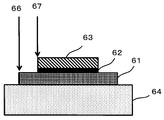
- FIG. 20 is a schematic cross-sectional view illustrating the side etching in the example.
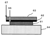
- FIG. 21 is a schematic cross-sectional view illustrating eaves in the example.
- the inventors of the present invention have made extensive studies to solve the above problems.
- the laminated film of the present invention is made of Ag, Al, Cu, or an alloy based on these as the first layer and has an electrical resistivity of 1.0 ⁇ 10 ⁇ 5 ⁇ ⁇ cm or less.
- the present invention further includes an oxide film containing at least one element selected from the group consisting of In, Zn, Sn and Al as the third layer in addition to the first layer and the second layer,
- the visible light reflectance of the three-layer laminated film of the first layer, the second layer, and the third layer is 30% or less, and the sheet resistance of the three-layer laminated film is 1.0 ⁇ / ⁇ or less.
- a laminated film is also included.
- the nitrogen-containing Cu alloy film having a reflectance of 45% or less at a wavelength of 650 nm and a light absorptance of 40% or more at a wavelength of 650 nm when the film thickness is 50 nm Contributes to improved workability.
- the two-layer laminated film and the three-layer laminated film containing the nitrogen-containing Cu alloy film as the second layer exhibit low electrical resistance, improve visibility, and have excellent wiring processability. And found that it can be applied to low reflection wiring.
- the first layer of the present invention is used as a conductive film, for example. Therefore, the first layer can be used as long as it is a metal material having an electric resistivity of 10 ⁇ ⁇ cm or less, and a material made of Ag, Al, Cu, or an alloy based on these can be used. . Among these, it is preferable to use either a Cu film or a Cu alloy film which is low in resistance and inexpensive.
- the electrical resistivity of the first layer is preferably 5.0 ⁇ ⁇ cm or less.
- the electrical resistivity of the first layer is as follows: electrical resistivity of the second layer serving as a light absorption layer: about 1 m ⁇ ⁇ cm, electrical resistivity of the third layer serving as an optical adjustment layer: about several hundreds Since it is smaller than ⁇ ⁇ cm, the current mainly passes through the first layer. Therefore, the sheet resistance of the laminated film itself is a value close to the electrical resistivity of the first layer that is the conductive film.
- the first layer is preferably a Cu alloy film containing at least one Z element selected from the group consisting of Mn, Ni, Co, Ge, Zn and Ti. By including the Z element, adhesion between the first layer and the substrate or another layer can be enhanced. Examples of the Cu alloy film in the first layer include those containing the Z element with the balance being Cu and inevitable impurities.
- the film thickness of the first layer is preferably 40 nm or more in order to achieve a sheet resistance value of the laminated film: 1.0 ⁇ / ⁇ or less.
- the film thickness of the first layer is more preferably 70 nm or more.
- the thickness of the first layer is preferably 400 nm or less, more preferably 300 nm or less.
- the second layer is stacked on the first layer, which is a conductive layer, to absorb incident light and to serve as a light absorption layer that suppresses reflected light.
- the second layer serving as a light absorbing layer As the second layer serving as a light absorbing layer like this, in the present invention, (I) Cu film having a reflectance of 45 nm or less at a wavelength of 650 nm at a film thickness of 50 nm and having a light absorption rate of 40% or more at a wavelength of 650 nm, or a partially nitrided Cu film; or (ii) a film thickness of 50 nm
- a Cu alloy film having a part of the nitrided film, which will be described in detail below, has a reflectance of 45% or less at a wavelength of 650 nm and a light absorption of 40% or more at a wavelength of 650 nm.
- the film (i) may be referred to as a “nitrogen-containing Cu film” or a “CuN film”.
- the “part of the film is nitrided” means that at least nitrogen is contained in the Cu film or the Cu alloy film described later, and it is not necessarily limited to only the nitride of Cu having a stoichiometric composition. There is no need to be configured. That is, when the Cu nitride is expressed as Cu—Ny, for example, y may be 0.1 at%.
- the nitrogen concentration in the second layer may be constant in the second layer or may have a concentration distribution.
- the second layer basically serves only as an optical adjustment of the laminated structure, and as long as it has a prescribed reflectance and light absorption rate, the nitrogen content in the second layer and its Distribution is not a problem.
- the second layer has a reflectance of 45% at a wavelength of 650 nm in the case of a film thickness of 50 nm so as to serve as a light absorption layer as described above.
- the light absorptance at a wavelength of 650 nm needs to satisfy 40% or more.
- the reflectance is preferably 40% or less, more preferably 35% or less.
- the light absorption rate is preferably 45% or more.
- the laminated film of the present invention when used as a low reflection wiring, it is also required to have excellent wiring workability.
- the wiring processability of the laminated film is mainly determined by the etching rate difference between the first layer and the second layer.
- the second layer has a higher etching rate than the first layer, and is evaluated in the examples described later.
- Side etching width or eaves width tends to increase. Therefore, in order to obtain a good wiring shape, the etching rates of the first layer and the second layer need to be close to each other.
- the inventors of the present invention have intensively studied to obtain a film having low electrical resistance, low reflection, and good wiring workability. As a result, excellent wiring processability can be easily obtained if the film contains at least one X element selected from Ni and Al, the remainder being Cu and inevitable impurities, and a part of the film is nitrided. I found.
- this partially nitrided Cu alloy film may be referred to as “nitrogen-containing Cu alloy film” or “Cu—XN film”.
- X of the “Cu—X—N film” is one or more of Ni and Al.
- the etching rate can be made slower than the case where the X element is not included, and as a result, the wiring processability can be improved.
- These elements may be used alone or in combination of two kinds.
- a nitrogen component containing Ni as an X element and the balance being Cu and inevitable impurities or a nitrogen containing Cu alloy film in which the metal component contains Al as an X element and the balance being Cu and inevitable impurities An alloy film is mentioned.
- Ni and Al are preferable to contain both Ni and Al as the X element.
- a nitrogen-containing Cu alloy film in which the metal component contains both Ni and Al as the X element and the balance is Cu and inevitable impurities is preferably used.
- the preferable content of the X element is preferably 5 atomic% or more, more preferably 10 atomic% or more, and further preferably 20 atomic% or more. Even if Ni is contained excessively, the effect of improving the wiring workability is saturated. On the other hand, since Ni is expensive, when there is much content, it will lead to the increase in material cost. Further, since Ni is an element having magnetism, when the content is large, there is a problem that DC discharge becomes difficult and the process time increases in the sputtering method optimal as the method for forming this nitrogen-containing Cu alloy film. Therefore, the upper limit of the Ni content is preferably 70 atomic percent or less, and more preferably 50 atomic percent or less.
- the Al content is preferably 3 atomic% or more, more preferably 4.5 atomic% or more, further preferably 7 atomic% or more, particularly preferably 15 It is at least atomic percent.
- the upper limit can be set to 40 atomic%.
- the film thickness of the second layer can be, for example, in the range of 10 nm to 300 nm in both cases (i) and (ii).
- the visible light reflectance of the two-layer laminated film of the first layer and the second layer is 45% or less, and the sheet resistance of the two-layer laminated film is 1. 0 ⁇ / ⁇ or less.
- the laminated film is useful as a low reflective conductive film.
- the wiring workability can be improved by controlling the ratio between the thickness of the first layer and the thickness of the second layer.
- the first layer thickness / second layer thickness is preferably 1.4 or less.
- a more preferable first layer thickness / second layer thickness is 1.0 or less.
- the etching rate is slowed by the addition of an alloy element such as Ni or Al, thereby improving the wiring workability.
- it is effective to control the laminated structure, specifically, the ratio of the film thickness of the first layer and the film thickness of the second layer, as described below, in order to ensure excellent wiring processability.
- FIG. 1 shows the amount of Ni and the ratio of the film thickness of the first layer and the film thickness of the second layer when the absolute value of the side etching width is 5.0 ⁇ m when the wiring is processed by the method of the embodiment described later. That is, the relationship between the first layer thickness / second layer thickness is shown by plots and approximate curves.
- the Ni amount is shown as the Ni addition amount.
- the area below the approximate curve is an area where the absolute value of the side etching width is less than 5.0 ⁇ m, and the area above the approximate curve is an absolute value of the side etching width of more than 5.0 ⁇ m. It is an area.
- FIG. 2 shows the amount of Al and the ratio of the thickness of the first layer to the thickness of the second layer when the side etching width becomes 5.0 ⁇ m when the wiring is processed, that is, the thickness of the first layer / the first layer.
- the relationship with the two-layer film thickness is shown by plots and approximate curves.
- the Al amount is shown as the Al addition amount.
- the region below the approximate curve is a region where the side etching width is less than 5 ⁇ m
- the region above the approximate curve is a region where the side etching width is greater than 5 ⁇ m.
- the first layer thickness / The two-layer film thickness needs to be 1.0 or less. If the film thickness of the first layer is reduced to satisfy this ratio, the conductivity of the laminated film tends to decrease. On the other hand, if the film thickness of the second layer is increased, the film formation time increases and the process cost increases. Tend to. For these reasons, the amount of Al is preferably 3 atomic% or more as described above.
- the third layer of the present invention is used as an optical adjustment layer, for example, and contributes to the realization of a low reflectance together with the second layer described above.
- This third layer is an oxide film containing at least one element selected from the group consisting of In, Zn, Sn, and Al.
- An oxide film containing at least In is preferable.
- ITO As In—Sn—O, IZO as In—Zn—O, ZnO, ZTO as Zn—Sn—O, ZAO as Zn—Al—O, or the like is preferably used.
- the film thickness of the third layer can be in the range of 10 nm to 300 nm, for example.
- the laminated film of the present invention essentially includes the first layer and the second layer, and further includes the third layer as necessary.
- the laminated film of the present invention may further have other layers.
- a film made of general Mo, Ni, Ti, Cr or an alloy based on these, preferably a Mo film may be formed as the adhesion layer.
- a Mo film can be formed on at least one surface of the second layer.
- the thickness of the adhesion layer can be set to, for example, 5 to 30 nm.
- the three-layer laminated film of the present invention including the first layer, the second layer, and the third layer has a visible light reflectance of 30% of the three-layer laminated film including the first layer, the second layer, and the third layer.
- the sheet resistance of the three-layer laminated film is 1.0 ⁇ / ⁇ or less. This three-layer-containing laminated film is useful as a low reflection conductive film or a low reflection wiring.
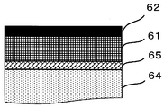
- FIG. 3 is a schematic sectional view showing a structural example of the laminated film of the present invention.
- a first layer 61 and a second layer 62 are sequentially laminated on a substrate 64 which is a transparent substrate.
- the said transparent substrate is normally used for the technical field of this invention, and will not be specifically limited if it has transparency, A glass substrate and a resin substrate can be used.
- the transparent substrate may be simply referred to as “substrate”.
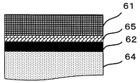
- FIG. 4 is a diagram showing another structural example of the laminated film of the present invention.
- a structure pattern opposite to that in FIG. 3, that is, a structure in which the second layer 62 and the first layer 61 are sequentially laminated on the substrate 64 may be used.
- the position of the second layer 62 provided as the light absorption layer is for the purpose of controlling the reflection of the first layer 61 which is a metal thin film. Therefore, the second layer 62 is formed on the light incident side of the first layer 61. That's fine.
- an adhesion layer 65 may be formed on at least one surface of the first layer 61.
- the material of the adhesion layer 65 include a film made of Mo, Ni, Ti, Cr, or an alloy based on these, and preferably a Mo film.
- an adhesion layer 65 can be provided between the substrate 64 and the first layer 61 or between the first layer 61 and the second layer 62.
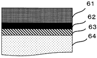
- FIG. 8 is a schematic sectional view showing another structural example of the laminated film of the present invention.
- a structure in which a first layer 61, a second layer 62, and a third layer 63 are sequentially stacked on a substrate 64 may be employed.
- FIG. 9 is a schematic sectional view showing another structural example of the laminated film of the present invention.
- a structure pattern opposite to that shown in FIG. 8, that is, a structure in which a third layer 63, a second layer 62, and a first layer 61 are sequentially stacked on a substrate 64 may be used.
- the position of the second layer 62 provided as the light absorption layer is for the purpose of controlling the reflection of the first layer 61 which is a metal thin film. Therefore, the second layer 62 is formed on the light incident side of the first layer 61. That's fine.
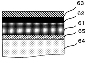
- FIG. 10 to FIG. 12 are diagrams showing other structural examples of the laminated film of the present invention.
- an adhesion layer 65 may be formed on at least one surface of the first layer 61.
- an adhesion layer 65 can be provided between the substrate 64 and the first layer 61 or between the first layer 61 and the second layer 62.
- the three-layer-containing laminated film of the present invention has a visible light reflectance of 30% or less and a sheet resistance of the laminated film of 1.0 ⁇ / ⁇ or less. In order to ensure the characteristics, for example, it is recommended to control the film thickness of the first layer as described above.
- the nitrogen-containing Cu alloy film or laminated film of the present invention is useful as a low reflection conductive film or low reflection wiring. Moreover, the nitrogen-containing Cu alloy film and laminated film of the present invention can be applied to an electromagnetic wave shield as well as a display device and an input device including a touch panel sensor. Below, the specific structure in the case of utilizing the laminated film of this invention for the wiring electrode of a touch panel, for example is demonstrated.
- liquid crystal display device part in the touch panel structure will be described.
- the present invention will be described using a liquid crystal display device as an example of the display device.
- the present invention is not limited to this, and can be applied to other display devices such as an organic EL display device.
- FIG. 13 is a schematic cross-sectional view schematically showing a configuration of a general liquid crystal display device.
- a liquid crystal display device 1 shown in FIG. 13 includes a thin film transistor (hereinafter referred to as TFT) substrate 2.
- the TFT substrate 2 is, for example, a TFT array substrate.
- a counter substrate 3 is disposed opposite to the TFT substrate 2. In FIG. 13, a thick arrow indicates the viewing direction.
- the counter substrate 3 is, for example, a color filter (CF, Color Filter) substrate 4 and is disposed on the side to be visually recognized.
- CF color filter
- BM black matrix
- BM black matrix
- a liquid crystal layer 7 into which liquid crystal is introduced is sandwiched between the TFT substrate 2 and the counter substrate 3, and the liquid crystal layer 7 is sealed with a liquid crystal sealing material 8. Furthermore, although not shown, a polarizing plate and a retardation plate are provided on the outer surface of the counter substrate 3. Further, although not shown, a backlight unit or the like is disposed on the non-viewing side of the liquid crystal display panel, that is, below the TFT substrate 2 in FIG.
- the input device including the electrode of the present invention is disposed above the color filter substrate 4 of the liquid crystal display device 1, that is, on the operation surface side.
- an electrode that can use the laminated film of the present invention from a transparent conductive film or the like, it may be referred to as a “metal electrode”.
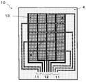
- FIG. 14 is a schematic plan view showing an example of an input device in a capacitive touch panel.
- the wiring has a lattice shape. More specifically, a plurality of driving metal electrodes arranged in the X direction for each row, that is, the driving electrodes 11 are arranged on the color filter substrate 4 which is a kind of transparent substrate; and arranged in the Y direction for each column. And a plurality of metal electrodes for detection, that is, detection electrodes 12 are provided.
- the drive electrode 11 and the detection electrode 12 are provided in different layers, and are insulated from each other by the insulating layer 13.
- a voltage is applied to the electrodes, and when the user touches the surface of the input device, the capacitance between the drive electrode 11 and the detection electrode 12 changes to generate a current. . By detecting this current with the drive electrode 11 and the detection electrode 12, the touch position of the user is detected.
- This configuration uses a metal electrode having a low resistance as the driving electrode 11 and the detection electrode 12, so that each electrode can be formed as a narrow wiring. Therefore, it has a feature that the transmittance of the active area can be sufficiently increased.
- the driving electrode 11 and the detection electrode 12 can be configured with narrow wiring, and high detection sensitivity and light transmittance can be secured at the same time.
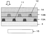
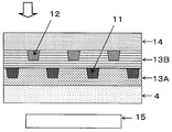
- FIG. 15 and FIG. 16 show examples of the sectional structure taken along the dotted line AA in FIG. 15 and 16 are schematic sectional views showing an example of a structure in which the input device 10 of FIG. 14 is mounted on the color filter substrate 4 of the liquid crystal display device 1 shown in FIG.
- a thick arrow indicates the direction of incident external light.
- a plurality of first metal electrodes 11 arranged in the X direction for each row are arranged on the same layer on the color filter substrate 4. Further, a plurality of second metal electrodes 12 arranged in the Y direction for each column are arranged in a different layer from the first metal electrode 11.
- the plurality of first metal electrodes 11 and second metal electrodes 12 are preferably arranged immediately above the black matrix, although not shown, in order not to deteriorate the visibility of the display device.
- the first insulating layer 13A Between the plurality of first metal electrodes 11, between the plurality of second metal electrodes 12, and between the first metal electrode 11 and the second metal electrode 12, the first insulating layer 13A, A second insulating layer 13B is disposed.
- first insulating layer 13A and the second insulating layer 13B for example, a known translucent insulating resin can be used. And the cover glass 14 is provided so that the surface in which the 2nd insulating layer 13B was provided may be covered.
- reference numeral 15 denotes a backlight.
- a metal electrode having excellent conductivity and low reflectivity is proposed. it can.
- FIG. 17 is a schematic plan view showing another example of the input device in the capacitive touch panel.
- the electrode is a diamond-shaped transparent electrode.
- the transparent substrate 33, a plurality of first electrode patterns 31A having a diamond shape arranged in the X direction for each row, and the first transparent electrode 31A are connected to the upper portion of the transparent substrate 33.
- One bridge electrode 31B, a plurality of second electrode patterns 32A having a diamond shape arranged in the Y direction for each column, and a second bridge electrode 32B for connecting the second transparent electrodes 32A are provided.
- the first transparent electrode composed of the first electrode pattern 31A and the bridge electrode 31B and the second transparent electrode composed of the second electrode pattern 32A and the bridge electrode 32B are insulated from each other by an insulating layer (not shown).
- Each electrode pattern is connected to a control unit (not shown) via the outer peripheral wiring 31C or 32C.
- a transparent conductive material is generally used for the first electrode pattern 31A and the second electrode pattern 32A.
- a metal oxide such as ITO that is In—Sn—O or IZO that is In—Zn—O can be given.
- An input device with high detection sensitivity is produced by using the laminated film of the present invention for the bridge electrodes 31B and 32B that connect the electrode patterns of the touch panel with this configuration and the outer peripheral wirings 31C and 32C of the input device. Can do.
- This configuration can be applied to an external input device type in which a cover glass, a touch panel, and a liquid crystal cell are individually manufactured and bonded, that is, an out-cell structure type liquid crystal display device.
- the out-cell structure has a simple manufacturing method and is widely used in liquid crystal display devices.
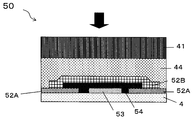
- FIGS. 18 and 19 Examples of the cross-sectional structure taken along the dotted line BB in FIG. 17 are shown in FIGS.
- the thick arrows in FIGS. 18 and 19 indicate the viewing direction.
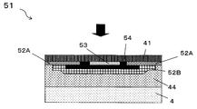
- a first transparent electrode 52A arranged in parallel to the X direction and a parallel to the Y direction are arranged on the color filter substrate 4 which is the first transparent substrate.
- a second transparent electrode 53 is provided on the color filter substrate 4 which is the first transparent substrate.
- the first transparent electrodes 52A, the second transparent electrodes 53, and the first transparent electrodes 52A and the second transparent electrodes 53 are separated from each other by the insulating layer 54 so that they do not contact each other.
- metal electrodes are provided as the transparent electrodes 52A and 53, the insulating layer 54, and the first bridge electrode 52B on the second transparent substrate, that is, the back surface side of the cover glass 41. This is different from FIG.
- the user's touch position is detected by detecting a current generated by a change in capacitance.
- the first bridge electrode 52B electrically connects the first transparent electrodes 52A.
- the adhesive layer 44 in FIGS. 18 and 19 is a layer that joins the cover glass 41, the color filter substrate 4, and the respective transparent electrodes, bridge electrodes, and the like.
- the adhesive layer is a transparent adhesive layer such as OCA (Optically Clear Adhesive, transparent adhesive sheet) or OCR (Optically Clear Resin, optical transparent resin), and an acrylic adhesive is used.
- the laminated film of the present invention can be suitably used as the first bridge electrode 52B in FIG. 18 or FIG.
- the bridge electrode 52B includes the two-layer-containing laminated film of any of FIGS. 3 to 7 including the second layer 62 and the first layer 61, or the third layer 63, the second layer 62, and the first layer 61.
- a metal electrode having excellent conductivity and low reflectance can be proposed.
- the laminated film of the present invention has a low sheet resistance and a low reflectance. Therefore, it can be applied not only to the electrodes used in the input region of the input device but also to the wiring on the outer periphery of the panel by extending the electrodes, and there is an advantage that the manufacturing process can be simplified.
- the two-layer-containing laminated film having the first layer and the second layer or the three-layer-containing laminated film having the first layer, the second layer, and the third layer is processed by wiring, and used as a metal electrode.
- the input device including the above is applied to a so-called on-cell structure formed between a liquid crystal color filter and a cover glass
- the present invention is not limited to this.
- a so-called out-cell structure in which an input device in which the sensor electrode of the touch panel is formed of a transparent conductive film and the bridge wiring between the transparent conductive films is formed of a metal electrode is formed separately from the liquid crystal cell.
- the present invention is not limited to this.
- the laminated film of the present invention can be applied to a so-called in-cell structure, for example, in a liquid crystal display device, for example, a liquid crystal display device in which an electrode of an input device is incorporated between a TFT substrate and a color filter substrate.
- a liquid crystal display device for example, a liquid crystal display device in which an electrode of an input device is incorporated between a TFT substrate and a color filter substrate.
- the input device to which the electrode using the laminated film of the present invention is applied includes an input device having an input means in a display device such as a touch panel or an input device having no display device such as a touch pad. Both are included. Specifically, an input device for operating the device by combining the above various display devices and position input means and pressing a display on the screen, or a display device separately installed corresponding to the input position on the position input means
- the laminated film of the present invention can also be used for an electrode of an input device for operation.
- sputtering is performed because of thinning, uniformity of alloy components in the film, easy control of the amount of added elements, high throughput during production, etc. It is preferable to form a film by a sputtering method using a target.
- the second layer in the laminated film of the present invention that is, the nitrogen-containing Cu film or the nitrogen-containing Cu alloy film
- a pure Cu sputtering target or a Cu alloy sputtering target having a desired alloy composition The method of forming by reactive sputtering method in the atmosphere containing nitrogen gas or nitrogen-containing gas is mentioned.
- two or more pure metal targets or alloy targets having different compositions may be used in place of the alloy sputtering target, and these may be discharged simultaneously to form the second layer.
- the sputtering target itself may be a material containing a Cu nitrogen compound or a Cu alloy nitrogen compound.
- the conditions of the reactive sputtering method for forming the second layer may be appropriately controlled according to the film thickness, film quality, and nitrogen concentration to be introduced. For example, in order to obtain a second layer satisfying a prescribed visible light reflectance or light absorption rate, it is possible to control the gas pressure during film formation.
- the shape of the sputtering target is not particularly limited, and an arbitrary shape such as a square plate shape, a circular plate shape, a donut plate shape, or a cylindrical shape can be used according to the shape or structure of the sputtering apparatus.
- the method for producing a nitrogen-containing Cu alloy film or laminated film of the present invention is particularly characterized by the film formation conditions for the second layer.
- a method for forming each layer other than the second layer that is, the first layer, the third layer, and other layers such as an adhesion layer included as necessary, a method usually used in the technical field of the present invention is appropriately adopted. Can do.
- a non-alkali glass plate having a thickness of 0.7 mm and a diameter of 4 inches was prepared, and the layers shown in Tables 1 to 5 were formed on the non-alkali glass plate by DC magnetron sputtering.
- a film was formed.
- Table 1 a sample was prepared in which a pure metal film or alloy film shown as the first layer in Tables 2 to 5 was formed on the alkali glass plate.
- Tables 2 and 3 a Cu film, an Al film or an Ag film is formed as the first layer on the alkali glass plate, and a CuN film or a Cu—X—N film shown in Table 2 or Table 3 is formed as the second layer in this order.
- a sample in which an IZO film, that is, an In—Zn—O film was formed as the second layer was also prepared as a comparative example.
- Tables 4 and 5 on the alkali glass plate, the Cu film, Cu alloy film, Al film or Ag film shown in Table 4 or Table 5 as the first layer, and the CuN film shown in Table 4 or Table 5 as the second layer.
- a sample was prepared in which a Cu—X—N film and an oxide film shown in Table 4 or 5 were formed as the third layer.
- IZO is In—Zn—O
- ITO is In—Sn—O
- ZTO is Zn—Sn—O
- ZAO Zn—Al—O.
- a sample was prepared in which the second layer CuN film or Cu—X—N film shown in Tables 2 to 5 was formed to a thickness of 50 nm on the alkali glass plate.
- the atmosphere in the chamber was once adjusted to an ultimate vacuum of 3 ⁇ 10 ⁇ 6 Torr before film formation, and then each layer was formed as shown below using a disk-type sputtering target having a diameter of 4 inches. A sample was obtained by sputtering.
- the film formation of the first layer was performed under the following conditions using a pure metal or alloy sputtering target having the same component composition as each of the first layers shown in Tables 1 to 5.
- Sputtering conditions Film forming method: Sputtering method Film forming apparatus: CS-200 manufactured by ULVAC Substrate temperature: room temperature Deposition gas: Ar gas Gas pressure: 2 mTorr Sputtering power: 10W to 500W Degree of vacuum: 1 ⁇ 10 -6 Torr or less
- Second Layer When a CuN film was formed as the second layer, a CuN film was formed by a reactive sputtering method using a pure Cu target and a mixed gas of Ar gas and N 2 gas. In the case where a Cu—X—N film was formed as the second layer, a plurality of sputtering targets containing an X element were used, the film formation power was adjusted so as to have a desired composition, and the film was formed by co-sputtering. In either case, the sputtering conditions are as follows.
- Film forming method Sputtering method
- Film forming apparatus CS-200 manufactured by ULVAC Substrate temperature: room temperature
- Deposition gas Ar gas and N 2 gas mixture gas pressure: 1 mTorr to 5 mTorr
- Sputter power 500 W in the case of film formation using one target having a desired composition.
- each target was set to an arbitrary power so as to have a desired composition.
- Degree of vacuum 1 ⁇ 10 -6 Torr or less
- the third layer is formed by a reactive sputtering method using an oxide target having the same component composition as the oxide film shown in Table 4 or Table 5, and using a mixed gas of Ar gas and O 2 gas. Filmed. Details of the oxide target and sputtering conditions are shown below.
- the electric resistivity of Cu film, Cu alloy film, Al film and Ag film used as the first layer of the laminated film in the present invention is as follows. Measured as follows. That is, the electrical resistivity was measured by a four-terminal method using a sample in which only the first layer was formed on the substrate by the above method. In this example, a material having an electric resistivity of 1.0 ⁇ 10 ⁇ 5 ⁇ ⁇ cm or less is accepted as a material suitable for the first layer, and the electric resistivity is 1.0 ⁇ 10 ⁇ 5 ⁇ ⁇ cm. Exceeded was rejected. The results are shown in Table 1. In Table 1, for example, No. “3.0E-06” of 1 means 3.0 ⁇ 10 ⁇ 6 . The same applies to the electrical resistivity shown in Tables 2 to 5 below.
- the electrical resistivity of the Cu film, Cu alloy film, Al film, and Ag film used as the first layer in this example was 1.0 ⁇ 10 ⁇ 5 ⁇ ⁇ cm or less.
- the reflectance and light absorption rate were measured with a spectrophotometer: V-570 manufactured by JASCO Corporation using a sample in which a CuN film or Cu—XN film formed as the second layer was formed to a thickness of 50 nm.
- V-570 manufactured by JASCO Corporation
- a reflectance at a wavelength of 650 nm of 45% or less and a light absorption at a wavelength of 650 nm of 40% or more was suitable as a light absorption layer.
- the visible light reflectance and sheet resistance of the two-layer laminated film of the first layer and the second layer, or the visible light reflection of the three-layer laminated film of the first layer, the second layer, and the third layer are used.
- Rate and sheet resistance were measured, but not limited to the above laminated structure, between the substrate and the first layer, between the first layer and the second layer, or between the second layer and the third layer, such as an adhesion layer Even when other layers are included, it has been separately confirmed that the visible light reflectance and sheet resistance satisfy the above acceptance criteria.
- the wiring workability of the laminated film was evaluated as follows. That is, using the sample of the above-mentioned two-layer laminated film or three-layer laminated film, wet etching processing was performed using an etching solution obtained by diluting Pure etch F108 made of Hayashi Pure Chemical Industries, Ltd. containing iron chloride 10 times with pure water. .
- the cross-sectional shape and planar shape of the sample subjected to the etching process were observed using an electron microscope S-4000 manufactured by Hitachi Power Solutions. Then, in the cross-sectional observation image, as schematically shown in FIG. 20, the one having the first layer end 66 longer than the second layer end 67 was determined as “side etching”. Further, as schematically shown in FIG. 21, a case where the first layer end 66 is shorter than the second layer end 67 is determined to be “eave”. Then, from the plane observation image, the side etching width and the eave width were measured, and the side etching width was determined as a negative number, and the eave width was determined as a positive number. The results are shown in the “wiring processability” column of Tables 2-5.
- the absolute value of the side etching width or the eave width is 5.0 ⁇ m or less, and it is shown as “A” in Tables 2 to 5 because it is excellent in the wiring processability of the laminated film and is passed. It was. On the other hand, in the cases where the absolute value is more than 5.0 ⁇ m, the wiring processability of the laminated film is inferior and is rejected.
- Tables 2 and 3 show the characteristics of the first layer and the two-layer laminated film in which the second layer is formed on the light incident side of the first layer.
- No. 1 is an example in which an IZO film having a reflectance of 45% or less as a second layer but having an absorptivity at a wavelength of 650 nm significantly lower than 40% is laminated.
- the visible light reflectance of the laminated film including this IZO film was also increased. In this way, No.
- the laminated film 1 does not have sufficient spectral characteristics and is not suitable as a low reflection conductive film or low reflection wiring.
- Nos. 3 to 7 are examples in which a CuN film having a reflectance of 45% or less and an absorptance of 40% or more is laminated as the second layer. In this way, the No. including the second layer having sufficient spectral characteristics.
- Each of the laminated films 3 to 7 has a low visible light reflectance and a low sheet resistance, and is suitable as a low reflection conductive film.
- No. 2 and No. No. 4 has the same film thickness as the component of the second layer and different optical characteristics because the gas pressure at the time of forming the second layer is different between the two.
- the first layer thickness / second layer thickness is preferably 1.4 or less, and more preferably 1.0 or less.
- Examples 8 to 16 are examples in which a Cu—Ni—N film having a reflectance of 45% or less and an absorptance of 40% or more is laminated as the second layer. In this way, the No. including the second layer having sufficient spectral characteristics. Any of the laminated films 8 to 16 has low visible light reflectance and low sheet resistance, and is suitable as a low reflective conductive film.
- the first layer thickness / second layer thickness or component composition is controlled. It turns out that it is good to do. That is, from the comparison with FIG. 1 described above, in order to ensure excellent wiring processability, the first layer thickness / second layer thickness is 1.4 or less when the Ni amount is 5.0 atomic%. When the Ni content is 7.0 atomic%, it is 1.4 or less, when the Ni content is 10.0 atomic%, it is 1.8 or less, and when the Ni content is 20.0 atomic%, it is 3 .6 or less is good. In addition, from the viewpoint of expanding the allowable film thickness range of the first layer and the second layer, the amount of Ni is preferably 5 atomic% or more, and more preferably 10 atomic% or more.
- Reference numerals 17 to 25 are examples in which a Cu—Al—N film having a reflectance of 45% or less and an absorption of 40% or more is laminated as the second layer. In this way, the No. including the second layer having sufficient spectral characteristics.
- the laminated films 17 to 25 all have low visible light reflectance and low sheet resistance, and are suitable as low reflection conductive films.
- the first layer thickness / second layer thickness or the composition of the components is controlled. It turns out that is good. That is, from the comparison with FIG. 2 described above, in order to ensure excellent wiring processability, the first layer thickness / second layer thickness is 2.0 or less when the Al amount is 7.2 atomic%. It can be seen that, when the Al content is 11.7 atomic%, it is preferably 3.0 or less, and when the Al content is 16.4 atomic%, it is preferable to set it to 3.6 or less.
- the Al content is preferably 3 atomic% or more, more preferably 7 atomic% or more, and further preferably 15 atomic% or more.
- No. in Table 3 Nos. 26 to 34 are examples in which a Cu—Ni—Al—N film having a reflectance of 45% or less and an absorptance of 40% or more is laminated as the second layer. In this way, the No. including the second layer having sufficient spectral characteristics.
- the laminated films 26 to 34 all have low visible light reflectance and low sheet resistance, and are suitable as low reflection conductive films. No.
- the laminated films 26 to 34 have excellent wiring processability and are useful as low reflection wiring. As described above, it is considered that the inclusion of both Ni and Al slows the etching rate and improves the wiring workability.
- Reference numerals 35 and 36 show examples in which an Al film or an Ag film is used for the first layer. If the second layer is a film defined by the present invention, it can be seen that even if an Al film or an Ag film is used for the first layer, the obtained laminated film satisfies the characteristics required for a low reflective conductive film.
- Tables 4 and 5 show the characteristics of the first layer and the three-layer laminated film in which the second layer and the third layer are sequentially formed on the light incident side of the first layer.
- No. in Table 4 1 is an example in which a CuN film having a reflectivity at a wavelength of 650 nm of more than 45% and an absorptivity at a wavelength of 650 nm of less than 40% is stacked as the second layer.
- No. in Table 4 Nos. 2 to 7 are examples in which a CuN film having a reflectance of 45% or less and an absorption rate of 40% or more is laminated as the second layer. In this way, the No. including the second layer having sufficient spectral characteristics. Any of the laminated films 2 to 6 has low visible light reflectance and low sheet resistance, and is suitable as a low reflective conductive film. No. No. 7 had a high sheet resistance because the first layer was thin. In order to sufficiently reduce the sheet resistance of the laminated film, the film thickness of the first layer is, for example, 70 nm or more.
- the first layer thickness / second layer thickness is preferably 1.3 or less, and more preferably 1.0 or less.
- Examples 8 to 16 are examples in which a Cu—Ni—N film having a reflectance of 45% or less and an absorptance of 40% or more is laminated as the second layer. In this way, the No. including the second layer having sufficient spectral characteristics. Any of the laminated films 8 to 16 has low visible light reflectance and low sheet resistance, and is suitable as a low reflective conductive film.
- the first layer thickness / second layer thickness or component composition is controlled. It turns out that it is good to do. That is, from the above comparison, in order to ensure excellent wiring processability, the first layer thickness / second layer thickness should be 1.2 or less when the Ni content is 5.0 atomic%. When the Ni content is 7.0 atomic%, it is 1.6 or less, when the Ni content is 10.0 atomic%, it is 2.0 or less, and when the Ni content is 20.0 atomic%, it is 3.6 or less. You can see that it is good.
- the amount of Ni is preferably 5 atomic% or more, and more preferably 10 atomic% or more.
- Reference numerals 17 to 25 are examples in which a Cu—Al—N film having a reflectance of 45% or less and an absorption of 40% or more is laminated as the second layer. In this way, the No. including the second layer having sufficient spectral characteristics.
- the laminated films 17 to 25 all have low visible light reflectance and low sheet resistance, and are suitable as low reflection conductive films.
- the first layer thickness / second layer thickness or the composition of the components is controlled. It turns out that is good. That is, from the above comparison, in order to ensure excellent wiring processability, the first layer thickness / second layer thickness should be about 1.8 or less when the Al content is 7.2 atomic%. It is well understood that when the Al content is 11.7 atomic%, it is good to set it to 2.8 or less, and when the Al content is 16.4 atomic%, it should be 3.6 or less.
- the Al content is preferably 7 atomic% or more, and more preferably 15 atomic% or more.
- No. in Table 5 Nos. 26 to 34 are examples in which a Cu—Ni—Al—N film having a reflectance of 45% or less and an absorptance of 40% or more is laminated as the second layer. In this way, the No. including the second layer having sufficient spectral characteristics.
- the laminated films 26 to 34 all have low visible light reflectance and low sheet resistance, and are suitable as low reflection conductive films. No.
- the laminated films 26 to 34 have excellent wiring processability and are useful as low reflection wiring. As described above, it is considered that the inclusion of both Ni and Al slows the etching rate and improves the wiring workability.
- No. in Table 5 35 to 46 show examples in which various Cu alloy films are used for the first layer.
- the excellent optical characteristics required for the laminated film are low even if a Cu alloy film having any alloy composition shown in Table 5 is used as the first layer. It can be seen that the sheet resistance and excellent wiring processability are all satisfied.
- Table 5 47 and 48 show examples in which an Al film or an Ag film is used for the first layer. If the second layer is a film defined by the present invention, it can be seen that even if an Al film or an Ag film is used for the first layer, the obtained laminated film satisfies the characteristics required for a low reflective conductive film.
- Reference numerals 49 to 52 are examples in which the third layer acting as the optical adjustment layer is an ITO film, a ZnO film, a ZTO film, or a ZAO film. This No. From the results of 49 to 52, even when any of the above oxide films is laminated, all of the excellent optical characteristics, low sheet resistance and excellent wiring processability required for the laminated film are satisfied. I understand.
Landscapes
- Chemical & Material Sciences (AREA)
- Chemical Kinetics & Catalysis (AREA)
- Engineering & Computer Science (AREA)
- Materials Engineering (AREA)
- Mechanical Engineering (AREA)
- Metallurgy (AREA)
- Organic Chemistry (AREA)
- Laminated Bodies (AREA)
- Non-Insulated Conductors (AREA)
- Physical Vapour Deposition (AREA)
- Conductive Materials (AREA)
Abstract
高い導電性を示すと共に視認性が改善され、かつ配線加工性にも優れた、例えば低反射配線として有用な窒素含有Cu合金膜を提供する。該窒素含有Cu合金膜は、NiとAlから選択される少なくとも1種のX元素を含み、残部がCuおよび不可避不純物であり、膜の一部が窒化し、かつ、膜厚が50nmである場合の、波長650nmの反射率が45%以下であると共に、波長650nmの光吸収率が40%以上であることを特徴とする。
Description
本発明は、窒素含有Cu合金膜、積層膜、およびこれらの製造方法、ならびにCu合金スパッタリングターゲットに関する。
金属材料は高い導電性を示すが、反射率が高い。よって例えばタッチパネルのセンサー電極に、ITO薄膜よりも低抵抗を実現できる金属薄膜を、メッシュ状に加工した金属メッシュ配線が提案されている。しかし金属薄膜は、上述の通り反射率が高いため、該配線のメッシュパターンが可視化するといった課題がある。よって上記電極に金属薄膜を用いた場合、該金属薄膜からの反射を抑制することが求められる。この金属薄膜からの反射が抑制されることを、以下「視認性が改善される」ということがある。この視認性が改善された電極構造として、例えば下記特許文献1~3の技術が挙げられる。
例えば特許文献1には、基板上に相互離隔される複数の導電性パターンセルを形成し、前記導電性パターンセル上に絶縁層を形成し、前記絶縁層上に黒色の導電材料を用いて前記導電性パターンセルを相互接続するブリッジ電極を形成することを特徴とするタッチパネルの電極パターンの製造方法が示されている。前記ブリッジ電極は、Al、Au、Ag、Sn、Cr、Ni、TiまたはMgの金属を用い、薬品との反応により酸化、窒化、フッ化して、黒色化することが示されている。
上記特許文献1には、金属の黒色化処理によるブリッジ電極の反射率低減化技術は示されているが、電気抵抗率の低減は全く考慮されていない。そのため、上記技術では、金属酸化物により電極が高抵抗化する場合もあり、電極には不適である。また、上記特許文献1には、Ag窒化物やMg酸化物などのように反応性が高く取り扱いが困難であるか、微細加工が困難である金属も含まれており、実用性に欠けると思われる。
特許文献2には、配線部の金属光沢反射光によりタッチパネル下に配置されるディスプレイの視認性を低下することなく、メッシュ状としても2枚のフィルムの貼り合わせのズレが生じない透明導電性フィルムに適用することが可能な積層体が示されている。該積層体として、少なくとも黒化層を2層、基材を1層有する積層体が示されている。また前記黒化層として、窒化銅、酸化銅、窒化ニッケル、及び酸化ニッケルからなる群より選ばれる少なくとも1つを含む層が示されている。また黒化層は好ましくは、層の全体100原子%において、銅およびニッケルの合計含有量(原子数基準)が50原子%以上95原子%以下の層であり、かつ窒素および酸素の合計含有量(原子数基準)が5原子%以上50原子%以下の層であることが示されている。
特許文献3には、経時においても黒化の色調が変化することがなく、タッチパネル下に配置されるディスプレイの視認性を低下することがない透明導電性フィルムに適用することが可能な積層体が示されている。また該積層体は、黒化層中の窒化銅について、窒化銅の酸化物を構成する窒素原子数と窒化銅の非酸化物を構成する窒素原子数との合計を100原子%とした場合に、窒化銅の酸化物を構成する窒素原子数が1原子%以上50原子%以下であることが示されている。
本発明は上記の様な事情に着目してなされたものであって、その目的は、高い導電性を示すと共に、金属薄膜からの反射が抑制され視認性の改善された、低反射導電膜または低反射配線として有用な積層膜を提供することにある。
また、例えばサブミクロンパターンの配線等として用いる場合には、ウェットエッチング法による配線加工が一般に施される。特にCu系薄膜の加工には、塩化鉄を含むエッチング液が安価なエッチング液として利用される。この塩化鉄を含むエッチング液を用いた場合であっても配線加工を良好に行えることが求められる場合もある。以下、この「配線加工を良好に行うことができる」ことを「配線加工性に優れた」ということがある。本発明は、可視光域に高い光吸収率を有し光吸収膜として有用であって、上記の配線加工性にも優れた単層膜として、窒素含有Cu合金膜を提供することも目的とする。更には、該窒素含有Cu合金膜を有し、高い導電性を示すと共に視認性が改善され、かつ配線加工性にも優れた、低反射導電膜または低反射配線として有用な積層膜を提供することも目的とする。
上記課題を解決し得た本発明の窒素含有Cu合金膜は、NiとAlから選択される少なくとも1種のX元素を含み、残部がCuおよび不可避不純物であり、膜の一部が窒化し、かつ膜厚が50nmである場合の、波長650nmの反射率が45%以下であると共に、波長650nmの光吸収率が40%以上であるところに特徴がある。
また上記課題を解決し得た本発明の積層膜は、第1層として、Ag、Al、Cu、またはこれらを基とする合金のいずれかからなり、かつ電気抵抗率が1.0×10⁻⁵Ω・cm以下である膜と、第2層として、膜厚50nmにおける波長650nmの反射率が45%以下であって、波長650nmの光吸収率が40%以上である、膜の一部が窒化したCu膜とを有し、かつ第1層と第2層の2層積層膜の可視光反射率が45%以下であると共に、該2層積層膜のシート抵抗が1.0Ω/□以下であるところに特徴がある。前記可視光反射率とは、後述する実施例に示す通り、波長450nm、550nm、650nmの全ての波長の反射率をいう。以下同じである。
また上記課題を解決し得た本発明の別の積層膜は、第1層として、Ag、Al、Cu、またはこれらを基とする合金のいずれかからなり、かつ電気抵抗率が1.0×10⁻⁵Ω・cm以下である膜と、第2層として、膜厚50nmにおける波長650nmの反射率が45%以下であって、波長650nmの光吸収率が40%以上である、膜の一部が窒化したCu膜と、第3層として、In、Zn、SnおよびAlよりなる群から選択される少なくとも1種の元素を含む酸化物膜とを有し、かつ前記第1層、第2層および第3層の3層積層膜の可視光反射率が30%以下であると共に、該3層積層膜のシート抵抗が1.0Ω/□以下であるところに特徴がある。
また上記課題を解決し得た本発明の別の積層膜は、第1層として、Ag、Al、Cu、またはこれらを基とする合金のいずれかからなり、かつ電気抵抗率が1.0×10⁻⁵Ω・cm以下である膜と、第2層として、前記窒素含有Cu合金膜とを有し、かつ第1層と第2層の2層積層膜の可視光反射率が45%以下であると共に、該2層積層膜のシート抵抗が1.0Ω/□以下であるところに特徴がある。
また上記課題を解決し得た本発明の別の積層膜は、第1層として、Ag、Al、Cu、またはこれらを基とする合金のいずれかからなり、かつ電気抵抗率が1.0×10⁻⁵Ω・cm以下である膜と、第2層として、前記窒素含有Cu合金膜と、第3層として、In、Zn、SnおよびAlよりなる群から選択される少なくとも1種の元素を含む酸化物膜とを有し、かつ前記第1層、第2層および第3層の3層積層膜の可視光反射率が30%以下であると共に、該3層積層膜のシート抵抗が1.0Ω/□以下であるところに特徴がある。
前記第1層は、Mn、Ni、Co、Ge、ZnおよびTiよりなる群から選択される少なくとも1種のZ元素を含むCu合金膜であることが好ましい。
前記第3層は、少なくともInを含む酸化物膜であることが好ましい。また、前記第1層の膜厚は40~400nmであることが好ましい。
本発明は、前記窒素含有Cu合金膜を有する低反射導電膜または低反射配線や、前記積層膜を有する低反射導電膜または低反射配線を含みうる。また本発明には、前記窒素含有Cu合金膜や前記積層膜を、例えば前記低反射導電膜または低反射配線として含みうる、表示装置、タッチパネルセンサーおよび電磁波シールドも包含する。更に本発明には、前記窒素含有Cu合金膜を形成するためのCu合金スパッタリングターゲットも含まれる。
本発明は更に、前記窒素含有Cu合金膜または積層膜を製造する方法も包含する。該方法は、前記窒素含有Cu合金膜または前記膜の一部が窒化したCu膜を、窒素ガスまたは窒素含有ガスを含む雰囲気下で反応性スパッタリング法により形成するところに特徴を有する。
本発明によれば、高い導電性を示すと共に視認性の改善された、低反射導電膜または低反射配線として有用な積層膜を提供できる。また、可視光域に高い光吸収率を有し光吸収膜として有用であり、かつ配線加工性にも優れた単層膜として窒素含有Cu合金膜を提供できる。更には、前記窒素含有Cu合金膜を有し、高い導電性を示すと共に視認性が改善され、かつ配線加工性にも優れた、低反射導電膜または低反射配線として有用な積層膜を提案できる。本発明の積層膜は、上記の通り配線加工性にも優れているので、ウェットエッチング法にて塩化鉄を含むエッチング液を用いた場合であっても、良好な配線形状、例えばサブミクロンパターンの配線を得ることができる。
本発明者らは、前記課題を解決するために鋭意研究を重ねた。その結果、まず、低電気抵抗であって高い導電性を有すると共に、金属薄膜部分からの反射が抑制され視認性の改善された、上記先行技術とは異なる低反射積層膜として、下記の積層膜を見出した。即ち、本発明の積層膜は、第1層として、Ag、Al、Cu、またはこれらを基とする合金のいずれかからなり、かつ電気抵抗率が1.0×10⁻⁵Ω・cm以下である膜;と、第2層として、膜厚50nmにおける波長650nmの反射率が45%以下であって、波長650nmの光吸収率が40%以上である、膜の一部が窒化したCu膜;とを有し、かつ第1層と第2層の2層積層膜の可視光反射率が45%以下であると共に、該2層積層膜のシート抵抗が1.0Ω/□以下であることを特徴とする。
本発明には更に、上記第1層、第2層に加え、第3層としてIn、Zn、SnおよびAlよりなる群から選択される少なくとも1種の元素を含む酸化物膜とを有し、第1層、第2層および第3層の3層積層膜の可視光反射率が30%以下であると共に、該3層積層膜のシート抵抗が1.0Ω/□以下であることを特徴とする積層膜も含まれる。
また規定の合金元素を含み、膜厚50nmの場合の、波長650nmでの反射率が45%以下であると共に、波長650nmでの光吸収率が40%以上である窒素含有Cu合金膜は、配線加工性の向上にも寄与する。本発明には更に、この窒素含有Cu合金膜を前記第2層として含む2層積層膜や3層積層膜が、低電気抵抗を示しかつ視認性が改善されると共に、優れた配線加工性も示し、低反射配線にも適用できることを見出した。
以下、各層について詳しく説明する。
(第1層)
本発明の第1層は、例えば導電膜として用いられる。そのため第1層は、電気抵抗率が10μΩ・cm以下の金属材料であれば利用することができ、Ag、Al、Cu、またはこれらを基とする合金のいずれかからなる材料を用いることができる。この中でも低抵抗かつ安価であるCu膜またはCu合金膜のいずれかを利用することが好ましい。前記第1層の電気抵抗率は、5.0μΩ・cm以下であることが好ましい。この第1層の電気抵抗率は、光吸収層としての役割を担う第2層の電気抵抗率:約1mΩ・cm、光学調整層としての役割を担う第3層の電気抵抗率:約数百μΩ・cmよりも小さいため、電流は主として第1層を経由する。そのため積層膜自体のシート抵抗は導電膜である第1層の電気抵抗率に近い値となる。
本発明の第1層は、例えば導電膜として用いられる。そのため第1層は、電気抵抗率が10μΩ・cm以下の金属材料であれば利用することができ、Ag、Al、Cu、またはこれらを基とする合金のいずれかからなる材料を用いることができる。この中でも低抵抗かつ安価であるCu膜またはCu合金膜のいずれかを利用することが好ましい。前記第1層の電気抵抗率は、5.0μΩ・cm以下であることが好ましい。この第1層の電気抵抗率は、光吸収層としての役割を担う第2層の電気抵抗率:約1mΩ・cm、光学調整層としての役割を担う第3層の電気抵抗率:約数百μΩ・cmよりも小さいため、電流は主として第1層を経由する。そのため積層膜自体のシート抵抗は導電膜である第1層の電気抵抗率に近い値となる。
第1層は、Mn、Ni、Co、Ge、ZnおよびTiよりなる群から選択される少なくとも1種のZ元素を含むCu合金膜であることが好ましい。前記Z元素を含むことによって、第1層と基板または他の層との密着性を高めることができる。上記第1層におけるCu合金膜として、上記Z元素を含み、残部がCuおよび不可避不純物からなるものが挙げられる。
第1層の膜厚は、積層膜のシート抵抗値:1.0Ω/□以下を達成するため、40nm以上であることが好ましい。第1層の膜厚は、より好ましくは70nm以上である。一方、第1層の膜厚が厚すぎると、成膜にかかる時間が長くなりプロセス時間が長くなる。その結果、材料コストの増加も招く。またウェットエッチング法による加工性や歩留まりが低下する。よって第1層の膜厚は400nm以下であることが好ましく、より好ましくは300nm以下である。
(第2層)
第2層は、導電層である第1層上に積層することで入射光を吸収し、反射光を抑える光吸収層としての役割を担う。
第2層は、導電層である第1層上に積層することで入射光を吸収し、反射光を抑える光吸収層としての役割を担う。
この様な光吸収層としての役割を担う第2層として、本発明では、
(i)膜厚50nmにおける波長650nmの反射率が45%以下であって、波長650nmの光吸収率が40%以上である、膜の一部が窒化したCu膜;または
(ii)膜厚50nmにおける波長650nmの反射率が45%以下であって、波長650nmの光吸収率が40%以上である、下記に詳述する、膜の一部が窒化したCu合金膜;を用いる。以下、上記(i)の膜を「窒素含有Cu膜」または「CuN膜」ということがある。
(i)膜厚50nmにおける波長650nmの反射率が45%以下であって、波長650nmの光吸収率が40%以上である、膜の一部が窒化したCu膜;または
(ii)膜厚50nmにおける波長650nmの反射率が45%以下であって、波長650nmの光吸収率が40%以上である、下記に詳述する、膜の一部が窒化したCu合金膜;を用いる。以下、上記(i)の膜を「窒素含有Cu膜」または「CuN膜」ということがある。
まず上記(i)と(ii)の膜の窒化について説明する。本発明において、前記「膜の一部が窒化」とは、Cu膜中または後記のCu合金膜中に少なくとも窒素が含有されていれば良く、必ずしも、化学量論組成のCuの窒化物のみから構成される必要はない。すなわち、上記Cuの窒化物をCu-Nyと表した場合、例えばyは0.1at%であってもよい。
上記第2層中の窒素濃度は、第2層内で一定であってもよいし、濃度分布があってもよい。本発明において上記第2層は、基本的に積層構造の光学調整としての役割を担っているのみであり、規定の反射率および光吸収率を有する限り、第2層中の窒素含有量やその分布は問題としない。
上記第2層は、上記(i)と(ii)のいずれの膜の場合も、上述の通り光吸収層としての役割を担うべく、膜厚50nmの場合の、波長650nmの反射率が45%以下であると共に、波長650nmの光吸収率が40%以上を満たす必要がある。前記反射率は好ましくは40%以下であり、より好ましくは35%以下である。前記光吸収率は好ましくは45%以上である。
次に、上記(ii)の膜について詳述する。
前述の通り、本発明の積層膜を、特に低反射配線として使用する場合、配線加工性に優れていることも求められる。積層膜の配線加工性は、主に第1層と第2層のエッチングレート差によって決まる。例えば第1層がCu系膜、第2層が窒素含有Cu膜である積層膜の場合、上記第1層よりも上記第2層の方が、エッチングレートが早く、後述する実施例で評価するサイドエッチング幅またはひさし幅が大きくなりやすい。よって、良好な配線形状を得るには第1層と第2層のエッチングレートを近づける必要がある。
本発明者らは、低電気抵抗、低反射であると共に、配線加工性も良好な膜を得るべく鋭意研究を行った。その結果、NiとAlから選択される少なくとも1種のX元素を含み、残部がCuおよび不可避不純物であり、膜の一部が窒化した膜とすれば、優れた配線加工性が得られやすいことを見出した。以下、この一部が窒化したCu合金膜を「窒素含有Cu合金膜」または「Cu-X-N膜」ということがある。前記「Cu-X-N膜」のXは、NiとAlのうちの1以上である。
上記NiとAlから選択される少なくとも1種のX元素を含むことによって、このX元素を含まない場合よりもエッチングレートを遅くすることができ、その結果、配線加工性を改善することができる。これらの元素は、単独で用いてもよいし2種を併用してもよい。例えば、金属成分が、X元素としてNiを含み、残部がCuおよび不可避不純物である窒素含有Cu合金膜や、金属成分が、X元素としてAlを含み、残部がCuおよび不可避不純物である窒素含有Cu合金膜が挙げられる。
[規則91に基づく訂正 25.05.2016]
X元素としてNiとAlの両方を含有させることが好ましい。例えば、金属成分が、X元素としてNiとAlの両方を含み、残部がCuおよび不可避不純物である窒素含有Cu合金膜が好ましく用いられる。
X元素としてNiとAlの両方を含有させることが好ましい。例えば、金属成分が、X元素としてNiとAlの両方を含み、残部がCuおよび不可避不純物である窒素含有Cu合金膜が好ましく用いられる。
X元素の好ましい含有量は、Niの場合、5原子%以上であることが好ましく、より好ましくは10原子%以上、更に好ましくは20原子%以上である。Niは過剰に含有させても上記配線加工性の改善効果は飽和する。一方、Niは高価であるため、含有量が多い場合、材料コストの増加に繋がる。またNiは磁性を有する元素であるため、含有量が多い場合、この窒素含有Cu合金膜の形成方法として最適なスパッタリング法において、DC放電が困難となり、プロセス時間が増加するといった問題が生じうる。よってNi含有量の上限は70原子%以下であることが好ましく、より好ましくは50原子%以下である。
X元素としてAlを含む場合、Al含有量は3原子%以上であることが好ましく、4.5原子%以上であることがより好ましく、7原子%以上であることが更に好ましく、特に好ましくは15原子%以上である。また例えば上限を40原子%とすることができる。
上記第2層の膜厚は、上記(i)と(ii)のいずれの膜の場合も、例えば10nm~300nmの範囲とすることができる。
(2層含有積層膜)
上記第1層と第2層を含む積層膜は、第1層と第2層の2層積層膜の可視光反射率が45%以下であると共に、該2層積層膜のシート抵抗が1.0Ω/□以下である。上記積層膜は、低反射導電膜として有用である。
上記第1層と第2層を含む積層膜は、第1層と第2層の2層積層膜の可視光反射率が45%以下であると共に、該2層積層膜のシート抵抗が1.0Ω/□以下である。上記積層膜は、低反射導電膜として有用である。
前述の通り、第1層がCu系膜であり、第2層が窒素含有Cu膜である積層膜の場合、上記第2層のサイドエッチング幅が大きくなりやすい。この場合、第1層の膜厚と第2層の膜厚の比率を制御することによって配線加工性を高めることができる。具体的には、第1層膜厚/第2層膜厚を1.4以下とすることが好ましい。より好ましい第1層膜厚/第2層膜厚は1.0以下である。
また前述の通り、第2層として窒素含有Cu合金膜を含む積層膜の場合、NiやAl等の合金元素の添加によりエッチングレートが遅くなるため、配線加工性が改善される。しかしより確実に優れた配線加工性を確保するには、下記の通り積層構造、具体的には第1層の膜厚と第2層の膜厚の比率を制御することが有効である。
例えば、第1層としてCu膜、第2層としてCu-Ni-N膜を用いた積層膜を例に説明する。図1は、後述する実施例の方法で配線加工した際にサイドエッチング幅の絶対値が5.0μmになるときの、Ni量と、第1層の膜厚と第2層の膜厚の比率、即ち、第1層膜厚/第2層膜厚との関係をプロットおよび近似曲線で示している。図1ではNi量をNi添加量と示している。この図1において、近似曲線よりも下側の領域はサイドエッチング幅の絶対値が5.0μm未満となる領域であり、近似曲線の上側の領域はサイドエッチング幅の絶対値が5.0μm超となる領域である。
この図1から、Ni添加量が5原子%よりも低い場合、優れた配線加工性を得る、即ち、サイドエッチング幅の絶対値を5.0μm以下とするには、第1層膜厚/第2層膜厚を1.2以下とする必要があることがわかる。この比率を満たすべく、第1層の膜厚を薄くすると、積層膜の導電性が低下する傾向にあり、一方、第2層の膜厚を厚くすると、成膜時間が長くかかりプロセスコストが増加する傾向にある。これらのことを考慮すると、Ni量は前述の通り5原子%以上であることが好ましい。
次に、第1層としてCu膜、第2層としてCu-Al-N膜を用いた積層膜を例に説明する。図2は、配線加工した際にサイドエッチング幅が5.0μmになるときの、Al量と、第1層の膜厚と第2層の膜厚の比率、即ち、第1層膜厚/第2層膜厚との関係をプロットおよび近似曲線で示している。図2ではAl量をAl添加量と示している。この図2において、近似曲線よりも下側の領域はサイドエッチング幅が5μm未満となる領域であり、近似曲線の上側の領域はサイドエッチング幅が5μm超となる領域である。
この図2から、Al添加量が3原子%よりも低い場合、優れた配線加工性を得る、即ち、サイドエッチング幅の絶対値を5.0μm以下とするには、第1層膜厚/第2層膜厚を1.0以下とする必要がある。この比率を満たすべく、第1層の膜厚を薄くすると、積層膜の導電性が低下する傾向にあり、一方、第2層の膜厚を厚くすると、成膜時間が長くかかりプロセスコストが増加する傾向にある。これらのことからAl量は、前述したとおり3原子%以上であることが好ましい。
尚、上記図1および図2は、第1層と第2層の2層積層膜に関するものである。配線加工性は、第1層と第2層の成分や膜厚によるため、該第1層と第2層に更に第3層や後述する密着層等の他の層が積層された積層膜についても、上記図1および図2と同様の結果が得られる。よってこの第3層等を更に含む積層膜の、第1層膜厚/第2層膜厚の好ましい範囲、Ni量の好ましい下限、およびAl量の好ましい下限は、上述した2層積層膜の場合と同じである。
(第3層)
本発明の第3層は、例えば光学調整層として用いられ、前述した第2層と共に、低反射率の実現に寄与する。この第3層は、In、Zn、SnおよびAlよりなる群から選択される少なくとも1種の元素を含む酸化物膜である。好ましくは少なくともInを含む酸化物膜である。該酸化物膜として、In-Sn-OであるITO、In-Zn-OであるIZO、ZnO、Zn-Sn-OであるZTO、Zn-Al-OであるZAOなどが好ましく用いられる。
本発明の第3層は、例えば光学調整層として用いられ、前述した第2層と共に、低反射率の実現に寄与する。この第3層は、In、Zn、SnおよびAlよりなる群から選択される少なくとも1種の元素を含む酸化物膜である。好ましくは少なくともInを含む酸化物膜である。該酸化物膜として、In-Sn-OであるITO、In-Zn-OであるIZO、ZnO、Zn-Sn-OであるZTO、Zn-Al-OであるZAOなどが好ましく用いられる。
上記第3層の膜厚は、例えば10nm~300nmの範囲とすることができる。該第3層の膜厚、材料組成、該第3層形成に用いる例えば蒸着法の条件などを最適化することによって、前述した第1層と第2層からの反射光の位相を調整し、積層膜の可視光反射率を低減し、またウェットエッチング法による配線加工性を高めることができる。
(3層含有積層膜)
本発明の積層膜は、上記第1層と第2層を必須とし、必要に応じて更に上記第3層を有する。また本発明の積層膜は、更に他の層を有していてもよい。例えば密着層として一般的なMo、Ni、Ti、Crまたはこれらを基とする合金からなる膜、好ましくはMo膜が形成されていてもよい。例えば前記第2層の少なくとも一方の面にMo膜を形成することができる。上記密着層を形成する場合、該密着層の厚さを例えば5~30nmとすることができる。
本発明の積層膜は、上記第1層と第2層を必須とし、必要に応じて更に上記第3層を有する。また本発明の積層膜は、更に他の層を有していてもよい。例えば密着層として一般的なMo、Ni、Ti、Crまたはこれらを基とする合金からなる膜、好ましくはMo膜が形成されていてもよい。例えば前記第2層の少なくとも一方の面にMo膜を形成することができる。上記密着層を形成する場合、該密着層の厚さを例えば5~30nmとすることができる。
これら第1層、第2層および第3層を含む本発明の3層含有積層膜は、前記第1層、第2層および第3層からなる3層積層膜の可視光反射率が30%以下を示すと共に、該3層積層膜のシート抵抗が1.0Ω/□以下を示すものである。この3層含有積層膜は、低反射導電膜または低反射配線として有用である。
次に、本発明の積層膜のとり得る積層形態について、図面を用いて説明する。
(2層含有積層膜の積層形態)
まずは、第1層と第2層を含む2層含有積層膜の積層形態について説明する。
まずは、第1層と第2層を含む2層含有積層膜の積層形態について説明する。
図3は、本発明の積層膜の構造例を示す概略断面図である。この図3に示すように、透明基板である基板64上に第1層61、第2層62が順に積層された構造が挙げられる。上記透明基板は、本発明の技術分野に通常用いられ、透明性を有するものであれば特に限定されず、ガラス基板や樹脂基板を使用することができる。また、フラットパネルディスプレイに利用する場合、例えば、カラーフィルタ基板やカバーガラスを構成するガラス基板、フィルム基板、プラスチック基板、石英基板などが挙げられる。上記透明基板を、以下、単に「基板」ということがある。
また図4は、本発明の積層膜の別の構造例を示す図である。この図4に示す通り、前記図3とは逆の構造パターン、即ち、基板64上に、第2層62、第1層61が順に積層された構造でもよい。光吸収層として設ける第2層62の位置は、金属薄膜である第1層61の反射制御を目的とするため、第1層61に光が入射する側に第2層62が形成されていればよい。
また、図5~図7は本発明の積層膜の別の構造例を示す概略断面図である。これらの図に示す通り、第1層61の少なくとも一方の面に例えば密着層65が形成されていてもよい。密着層65の材料は、密着層として一般的なMo、Ni、Ti、Crまたはこれらを基とする合金からなる膜が挙げられ、好ましくはMo膜である。詳細には図5~図7に示す通り基板64と第1層61の間や、第1層61と第2層62の間に、密着層65を設けることができる。
(3層含有積層膜の積層形態)
次に、第1層、第2層および第3層を含む3層含有積層膜の積層形態について説明する。尚、基板64、第1層61、第2層62、密着層65については、上記2層含有積層膜と同じであり、これら各層の詳細な説明を省略する。
次に、第1層、第2層および第3層を含む3層含有積層膜の積層形態について説明する。尚、基板64、第1層61、第2層62、密着層65については、上記2層含有積層膜と同じであり、これら各層の詳細な説明を省略する。
図8は、本発明の積層膜の別の構造例を示す概略断面図である。この図8に示す通り、基板64上に第1層61、第2層62、および第3層63が順に積層された構造でもよい。また図9は本発明の積層膜の別の構造例を示す概略断面図である。この図9に示す通り、前記図8とは逆の構造パターン、即ち、基板64上に第3層63、第2層62、第1層61が順に積層された構造でもよい。光吸収層として設ける第2層62の位置は、金属薄膜である第1層61の反射制御を目的とするため、第1層61に光が入射する側に第2層62が形成されていればよい。
また、図10~図12は本発明の積層膜の別の構造例を示す図である。これらの図に示す通り、第1層61の少なくとも一方の面に例えば密着層65が形成されていてもよい。詳細には図10~図12に示す通り基板64と第1層61の間や、第1層61と第2層62の間に、密着層65を設けることができる。
本発明の3層含有積層膜は、積層膜の可視光反射率が30%以下であると共に、積層膜のシート抵抗が1.0Ω/□以下である。該特性を確保するには、例えば第1層の膜厚を上述の通り制御すること等が推奨される。
以上、本発明の各層の成分や特性、および積層形態について説明した。
本発明の窒素含有Cu合金膜や積層膜は、低反射導電膜または低反射配線として有用である。また本発明の窒素含有Cu合金膜や積層膜は、表示装置や、タッチパネルセンサーを含む入力装置の他、電磁波シールドにも適用することができる。以下では、例えばタッチパネルの配線電極に、本発明の積層膜を利用する場合の具体的な構造を説明する。
まずタッチパネル構造における液晶表示装置部分について説明する。以下では表示装置として液晶表示装置を例に本発明を説明するが、本発明はこれに限定されず、例えば有機EL表示装置等の他の表示装置にも適用できる。
図13は、一般的な液晶表示装置の構成を模式的に示す概略断面図である。図13に示す液晶表示装置1は、薄膜トランジスタ(Thin Film Transistor、以下TFTと呼ぶ)基板2を有している。TFT基板2は、例えば、TFTアレイ基板である。TFT基板2には、対向基板3が対向して配置されている。図13において太矢印は視認方向を示している。対向基板3は、例えばカラーフィルタ(CF、Color Filter)基板4であり、視認される側に配置される。対向基板3には、緑色、青色、赤色のカラーフィルタ5A、5B、5C、ブラックマトリックス(Black Matrix、BM)6、カラーフィルタ基板4が形成される。TFT基板2と対向基板3との間には液晶が導入された液晶層7が狭持され、液晶層7は液晶封止材8により封止される。更に、対向基板3の外側の面には、図示しないが偏光板及び位相差板等が設けられる。また、液晶表示パネルの反視認側、即ち、図13におけるTFT基板2の下方には、図示しないがバックライトユニット等が配設される。
本発明の電極を含む入力装置、特にタッチパネルセンサーは、上記液晶表示装置1のカラーフィルタ基板4の上方、即ち、操作面側に配置される。
以下、上記入力装置のパターンを例示しながら、本発明の好ましい実施態様について説明する。本発明の積層膜を用いうる電極を、透明導電膜などと区別するために、「金属電極」と記載することがある。
(1)入力装置例その1
図14は、静電容量型のタッチパネルにおける入力装置の一例を示す概略平面図である。図14に示す入力装置10は、配線が格子形状となっている。詳細には、透明基板の一種であるカラーフィルタ基板4の上部に、行ごとにX方向に配置される駆動用の複数の金属電極、即ち駆動用電極11と;列ごとにY方向に配置される検出用の複数の金属電極、即ち検出用電極12と;が設けられる。駆動用電極11と検出用電極12とは、それぞれ異なる層に設けられており、絶縁層13により互いに絶縁される。
図14は、静電容量型のタッチパネルにおける入力装置の一例を示す概略平面図である。図14に示す入力装置10は、配線が格子形状となっている。詳細には、透明基板の一種であるカラーフィルタ基板4の上部に、行ごとにX方向に配置される駆動用の複数の金属電極、即ち駆動用電極11と;列ごとにY方向に配置される検出用の複数の金属電極、即ち検出用電極12と;が設けられる。駆動用電極11と検出用電極12とは、それぞれ異なる層に設けられており、絶縁層13により互いに絶縁される。
前記図14の構成では、電極に電圧が印加されており、ユーザが入力装置表面にタッチすることにより、駆動用電極11と検出用電極12との間の静電容量が変化して電流を生じる。この電流を駆動用電極11と検出用電極12で検知することによりユーザのタッチ位置が検出される。
本構成は、抵抗の小さい金属電極を駆動用電極11および検出用電極12として用いることから、それぞれの電極を幅の狭い配線として形成することが可能である。そのためアクティブエリアの透過率を十分高くすることができる特徴を有する。本構成では、電極として電気抵抗の低い積層膜を用いるので、駆動用電極11および検出用電極12を幅の狭い配線で構成できるとともに、高い検出感度と光透過率性を同時に確保できる。
前出の図14の点線A-Aにおける断面構造の例を図15および図16に示す。図15と図16は、図14の入力装置10を、図13に示す液晶表示装置1のカラーフィルタ基板4に搭載した構造の一例を示す概略断面図である。図15および図16において、太矢印は外光入射方向を示す。
図15および図16に示されるように、カラーフィルタ基板4の上部には、行ごとにX方向に配置される複数の第1の金属電極11が、同一の層に配置される。さらに列ごとにY方向に配置される複数の第2の金属電極12が、第1の金属電極11とは異なる層に配置される。この複数の第1の金属電極11と第2の金属電極12は、表示装置の視認性を低下させないために、図示していないがブラックマトリックスの直上に配置することが好ましい。複数の第1の金属電極11の間、複数の第2の金属電極12の間、および、第1の金属電極11と第2の金属電極12との間には、第1の絶縁層13A、第2の絶縁層13Bが配置される。第1の絶縁層13Aと第2の絶縁層13Bには、例えば公知の透光性絶縁樹脂などを用いることができる。そして第2の絶縁層13Bが設けられた面を覆うように、カバーガラス14が設けられる。尚、図15と図16における15はバックライトを示す。
図15および図16の第1の金属電極11や第2の金属電極12において、第2層62と第1層61を含む前記図3~図7のいずれかの2層含有積層膜、または、第3層63、第2層62および第1層61を含む前記図8~図12のいずれかの3層含有積層膜を用いることによって、導電性に優れ、かつ低反射率な金属電極を提案できる。
(2)入力装置例その2
図17は、静電容量型のタッチパネルにおける入力装置の別の一例を示す概略平面図である。図17の入力装置30では電極がダイヤ形状の透明電極となっている。詳細には、透明基板33と、透明基板33の上部に、行ごとにX方向に配置されるダイヤ形状を有する複数の第1の電極パターン31Aと、第1の透明電極31A間を接続する第1のブリッジ電極31Bと、列ごとにY方向に配置されるダイヤ形状を有する複数の第2の電極パターン32Aと、第2の透明電極32A間を接続する第2のブリッジ電極32Bが設けられる。第1の電極パターン31Aおよびブリッジ電極31Bからなる第1の透明電極と、第2の電極パターン32Aおよびブリッジ電極32Bからなる第2の透明電極とは、図示しない絶縁層により互いに絶縁される。それぞれの電極パターンは、外周配線31Cや32Cを介して、図示しない制御部に接続される。
図17は、静電容量型のタッチパネルにおける入力装置の別の一例を示す概略平面図である。図17の入力装置30では電極がダイヤ形状の透明電極となっている。詳細には、透明基板33と、透明基板33の上部に、行ごとにX方向に配置されるダイヤ形状を有する複数の第1の電極パターン31Aと、第1の透明電極31A間を接続する第1のブリッジ電極31Bと、列ごとにY方向に配置されるダイヤ形状を有する複数の第2の電極パターン32Aと、第2の透明電極32A間を接続する第2のブリッジ電極32Bが設けられる。第1の電極パターン31Aおよびブリッジ電極31Bからなる第1の透明電極と、第2の電極パターン32Aおよびブリッジ電極32Bからなる第2の透明電極とは、図示しない絶縁層により互いに絶縁される。それぞれの電極パターンは、外周配線31Cや32Cを介して、図示しない制御部に接続される。
図17の構成では、スクリーンへ指などが接触した際に、第1の電極パターン31Aと第2の電極パターン32Aとの間の静電容量が変化して電流が発生し、これをX方向の電極とY方向の電極で検知することにより、ユーザのタッチ位置が検出される。
第1の電極パターン31Aおよび第2の電極パターン32Aには、一般的に透明導電性材料が用いられる。具体的には例えば、In-Sn-OであるITOや、In-Zn-OであるIZOなどの金属酸化物が挙げられる。
本構成のタッチパネルの、それぞれの電極パターン間を接続するブリッジ電極31B、32Bや入力装置の外周配線31C、32Cに、本発明の積層膜を用いることにより、検出感度の高い入力装置を作製することができる。
本構成は、カバーガラス、タッチパネル、液晶セルを個別に作製・接着するタイプの入力装置外付型、すなわちアウトセル構造型の液晶表示装置に適用できる。アウトセル型構造は製造方法がシンプルであり、液晶表示装置に広範に使用されている。
前出の図17の点線B-Bにおける断面構造の例を図18および図19に示した。この図18および図19における太矢印は視認方向を示す。図18の断面構造50に示すように、第1の透明基板であるカラーフィルタ基板4上には、X方向に平行して配置される第1の透明電極52Aと、Y方向に平行して配置される第2の透明電極53が設けられる。第1の透明電極52A間、および第2の透明電極53間、第1の透明電極52Aと第2の透明電極53の間は、それぞれが接触しないよう、絶縁層54により分離される。図19の断面構造51では、第2の透明基板、即ちカバーガラス41の裏面側に、透明電極52Aや53、絶縁層54、および第1のブリッジ電極52Bとして金属電極が設けられており、この点が前記図18と異なる。ユーザのタッチ位置は、静電容量の変化により発生した電流を検知することにより検出される。図18および図19において、第1のブリッジ電極52Bは、第1の透明電極52A間を電気的に接続している。図18および図19の接着層44は、カバーガラス41と、カラーフィルタ基板4と、それぞれの透明電極およびブリッジ電極等とを接合する層である。接着層は、OCA(Optically Clear Adhesive、透明粘着シート)やOCR(Optically Clear Resin、光学透明樹脂)などの透明粘着層であり、アクリル系粘着材などが用いられる。
前記図18や前記図19における第1のブリッジ電極52Bとして、本発明の積層膜を好適に用いることができる。ブリッジ電極52Bにおいて、第2層62と第1層61を含む前記図3~図7のいずれかの2層含有積層膜、または、第3層63、第2層62および第1層61を含む前記図8~図12のいずれかの3層含有積層膜を用いることによって、導電性に優れ、かつ低反射率な金属電極を提案できる。
以上、本発明をタッチパネルのセンサー電極に利用するための具体例について詳述した。
上述したように本発明の積層膜は、低いシート抵抗と低い反射率を兼ね備えている。よって、入力装置の入力領域に用いられる電極のみならず、当該電極を延長してパネル外周部の配線にも適用可能であり、製造プロセスを簡素化できるというメリットがある。
前述した入力装置例その1では、第1層および第2層を有する2層含有積層膜または第1層、第2層および第3層を有する3層含有積層膜を配線加工し、金属電極として含む入力装置を、液晶のカラーフィルタとカバーガラスの間に形成する、いわゆるオンセル型構造に適用する例を示したが、本発明はこれに限定されない。
また前述した入力装置例その2では、タッチパネルのセンサー電極を透明導電膜とし、前記透明導電膜間のブリッジ配線を金属電極により形成する入力装置を、液晶セルとは別に形成する、いわゆるアウトセル型構造に適用する例を示したが、本発明はこれに限定されない。
本発明の積層膜は、例えば液晶表示装置内、例えばTFT基板とカラーフィルタ基板の間に入力装置の電極を組み込んだ液晶表示装置、いわゆるインセル型構造に適用することも可能である。このように本発明は前記実施の態様に限定されるものではなく、その要旨を逸脱しない範囲で種々の変更が可能であることはいうまでもない。
また本発明の積層膜を用いた電極が適用される入力装置には、タッチパネルなどのように表示装置に入力手段を備えた入力装置や、タッチパッドのような表示装置を有さない入力装置の両方が含まれる。具体的には上記各種表示装置と位置入力手段を組み合わせ、画面上の表示を押すことで機器を操作する入力装置や、位置入力手段上の入力位置に対応して別途設置されている、表示装置操作用の入力装置の電極にも本発明の積層膜を用いることができる。
本発明の窒素含有Cu合金膜や積層膜を得るには、細線化や膜内の合金成分の均一性、さらには添加元素量の制御の容易さ、製造時のスループットの高さなどから、スパッタリングターゲットを用いたスパッタリング法で成膜することが好ましい。
特に本発明の積層膜における第2層、即ち窒素含有Cu膜または窒素含有Cu合金膜を成膜する方法として、例えば、純Cuスパッタリングターゲット、または所望の合金組成を有するCu合金スパッタリングターゲットを用い、窒素ガスまたは窒素含有ガスを含む雰囲気下で反応性スパッタリング法により形成する方法が挙げられる。または、前記合金スパッタリングターゲットの代わりに、組成の異なる二つ以上の純金属ターゲットや合金ターゲットを用い、これらを同時に放電させて第2層を成膜してもよい。この場合、スパッタリングターゲット自体がCuの窒素化合物またはCu合金の窒素化合物を含有した材料であってもよい。
上記第2層を成膜するための反応性スパッタリング法の条件は、膜厚、膜質、導入したい窒素濃度に応じて適切に制御すればよい。例えば、規定の可視光反射率や光吸収率を満たす第2層を得るには、成膜時のガス圧を制御すること等が挙げられる。
スパッタリングターゲットの形状は特に限定されず、スパッタリング装置の形状や構造に応じて任意の形状、例えば角型プレート状、円形プレート状、ドーナツプレート状、円筒状などに加工したものを用いることができる。
本発明の窒素含有Cu合金膜または積層膜の製造方法は、特に上記第2層の成膜条件に特徴がある。上記第2層以外の各層、即ち第1層、第3層、必要に応じて含まれる密着層等その他の層の成膜方法は、本発明の技術分野において通常用いられる方法を適宜採用することができる。
本願は、2015年3月30日に出願された日本国特許出願第2015-069999号に基づく優先権の利益を主張するものである。2015年3月30日に出願された日本国特許出願第2015-069999号の明細書の全内容が、本願の参考のため援用される。
以下、実施例を挙げて本発明をより具体的に説明するが、本発明はもとより下記実施例によって制限を受けるものではなく、前・後記の趣旨に適合し得る範囲で適当に変更を加えて実施することも勿論可能であり、それらはいずれも本発明の技術的範囲に包含される。
(1)サンプルの作製
透明基板として、板厚0.7mm、直径4インチの無アルカリ硝子板を用意し、この無アルカリ硝子板上に、DCマグネトロンスパッタリング法により、表1~5に示す各層を成膜した。詳細には表1では、表2~5の第1層として示す純金属膜または合金膜を、上記アルカリ硝子板上に形成したサンプルを用意した。表2および表3では、上記アルカリ硝子板上に、第1層としてCu膜、Al膜またはAg膜、第2層として表2または表3に示すCuN膜またはCu-X-N膜を順に形成したサンプルを用意した。尚、第2層としてIZO膜、即ちIn-Zn-O膜を形成したサンプルも比較例として用意した。表4および表5では上記アルカリ硝子板上に、第1層として表4または表5に示すCu膜、Cu合金膜、Al膜またはAg膜、第2層として表4または表5に示すCuN膜またはCu-X-N膜、第3層として表4または表5に示す酸化物膜を形成したサンプルを用意した。尚、表4および表5において、IZOはIn-Zn-O、ITOはIn-Sn-O、ZTOはZn-Sn-O、ZAOはZn-Al-Oである。
透明基板として、板厚0.7mm、直径4インチの無アルカリ硝子板を用意し、この無アルカリ硝子板上に、DCマグネトロンスパッタリング法により、表1~5に示す各層を成膜した。詳細には表1では、表2~5の第1層として示す純金属膜または合金膜を、上記アルカリ硝子板上に形成したサンプルを用意した。表2および表3では、上記アルカリ硝子板上に、第1層としてCu膜、Al膜またはAg膜、第2層として表2または表3に示すCuN膜またはCu-X-N膜を順に形成したサンプルを用意した。尚、第2層としてIZO膜、即ちIn-Zn-O膜を形成したサンプルも比較例として用意した。表4および表5では上記アルカリ硝子板上に、第1層として表4または表5に示すCu膜、Cu合金膜、Al膜またはAg膜、第2層として表4または表5に示すCuN膜またはCu-X-N膜、第3層として表4または表5に示す酸化物膜を形成したサンプルを用意した。尚、表4および表5において、IZOはIn-Zn-O、ITOはIn-Sn-O、ZTOはZn-Sn-O、ZAOはZn-Al-Oである。
更に第2層の分光特性を評価するため、上記アルカリ硝子板上に、表2~5に示す第2層のCuN膜またはCu-X-N膜を膜厚50nm形成したサンプルも用意した。
成膜にあたっては、成膜前にチャンバー内の雰囲気を一旦、到達真空度:3×10⁻⁶Torrに調整してから、直径4インチの円盤型スパッタリングターゲットを用い、下記に示す通り、各層をスパッタリング法で形成してサンプルを得た。
第1層の成膜
第1層の成膜は、表1~5に示す各第1層と同じ成分組成の純金属または合金のスパッタリングターゲットを用い、下記の条件で行った。
スパッタリング条件
成膜方法:スパッタリング法
成膜装置:ULVAC社製 CS-200
基板温度:室温
成膜ガス:Arガス
ガス圧:2mTorr
スパッタパワー:10W~500W
真空到達度:1×10⁻⁶Torr以下
第1層の成膜は、表1~5に示す各第1層と同じ成分組成の純金属または合金のスパッタリングターゲットを用い、下記の条件で行った。
スパッタリング条件
成膜方法:スパッタリング法
成膜装置:ULVAC社製 CS-200
基板温度:室温
成膜ガス:Arガス
ガス圧:2mTorr
スパッタパワー:10W~500W
真空到達度:1×10⁻⁶Torr以下
第2層の成膜
第2層としてCuN膜を成膜する場合は、純Cuターゲットを用い、ArガスとN2ガスの混合ガスを用いた反応性スパッタリング法でCuN膜を成膜した。第2層としてCu-X-N膜を成膜する場合は、X元素を含むスパッタリングターゲットを複数用いて、所望の組成になるよう成膜パワーを調整し、コスパッタ法で成膜した。いずれの場合も、スパッタリング条件は以下の通りである。
スパッタリング条件
成膜方法:スパッタリング法
成膜装置:ULVAC社製 CS-200
基板温度:室温
成膜ガス:ArガスとN2ガスの混合ガス
ガス圧:1mTorr~5mTorr
スパッタパワー:所望の組成を有する1ターゲットを用いて成膜の場合は500Wとした。コスパッタ法で成膜の場合は、所望の組成になるよう各ターゲットを任意のパワーに設定した。
真空到達度:1×10⁻⁶Torr以下
第3層の成膜
第3層は、表4または表5に示す酸化物膜と同じ成分組成の酸化物ターゲットを用い、ArガスとO2ガスの混合ガスを用いた反応性スパッタリング法で成膜した。上記酸化物ターゲットの詳細とスパッタリング条件を下記に示す。
酸化物ターゲットの組成
IZOターゲット:In2O3-ZnO、質量比率はIn2O3:ZnO=90:10
ITOターゲット:In2O3-SnO2、質量比率はIn2O3:SnO=95:5
ZnOターゲット:ZnO
ZTOターゲット:ZnO-SnO2、質量比率はZnO:SnO2=90:10
ZAOターゲット:ZnO-Al2O3、質量比率はZnO:Al2O3=90:10
スパッタリング条件
成膜方法:スパッタリング法
成膜装置:ULVAC社製 CS-200
基板温度:室温
成膜ガス:ArガスとO2ガスの混合ガス
ガス圧:2mTorr
スパッタパワー:150W
真空到達度:1×10⁻⁶Torr以下
(2)抵抗の測定
(2-1)第1層の電気抵抗率の測定
本発明において積層膜の第1層として用いるCu膜、Cu合金膜、Al膜およびAg膜の電気抵抗率を、次の通り測定した。即ち、上記基板に上記方法で第1層のみを成膜したサンプルを用い、4端子法で電気抵抗率を測定した。そして本実施例では、電気抵抗率が1.0×10⁻⁵Ω・cm以下のものを第1層に適した材料として合格とし、電気抵抗率が1.0×10⁻⁵Ω・cmを超えるものを不合格とした。その結果を表1に示す。尚、表1において、例えばNo.1の「3.0E-06」は、3.0×10⁻⁶を意味する。以下、後記の表2~5に示された電気抵抗率についても同じである。
(2-1)第1層の電気抵抗率の測定
本発明において積層膜の第1層として用いるCu膜、Cu合金膜、Al膜およびAg膜の電気抵抗率を、次の通り測定した。即ち、上記基板に上記方法で第1層のみを成膜したサンプルを用い、4端子法で電気抵抗率を測定した。そして本実施例では、電気抵抗率が1.0×10⁻⁵Ω・cm以下のものを第1層に適した材料として合格とし、電気抵抗率が1.0×10⁻⁵Ω・cmを超えるものを不合格とした。その結果を表1に示す。尚、表1において、例えばNo.1の「3.0E-06」は、3.0×10⁻⁶を意味する。以下、後記の表2~5に示された電気抵抗率についても同じである。

この表1から本実施例で第1層として使用したCu膜、Cu合金膜、Al膜およびAg膜は、いずれも電気抵抗率が1.0×10⁻⁵Ω・cm以下であった。
(2-2)第2層の電気抵抗率の測定
第2層として形成したCuN膜またはCu-X-N膜の電気抵抗率を次の通り測定した。即ち、上記基板に上記方法で第2層のみを成膜した試料を用い、4端子法にて電気抵抗率を測定した。その結果を表2~5に示す。
第2層として形成したCuN膜またはCu-X-N膜の電気抵抗率を次の通り測定した。即ち、上記基板に上記方法で第2層のみを成膜した試料を用い、4端子法にて電気抵抗率を測定した。その結果を表2~5に示す。
(2-3)積層膜のシート抵抗の測定
第1層と第2層を積層させた表2および表3の2層積層膜と、第1層、第2層および第3層を積層させた表4および表5の3層積層膜の、シート抵抗を次の通り測定した。即ち、上記方法で測定したサンプルを用い、4端子法にてシート抵抗を測定した。そして本実施例では、シート抵抗が1.0Ω/□以下のものを合格として表2~5において「A」と示し、特に0.5Ω/□以下のものをより優れているとして表2~5において「AA」と示した。一方、前記シート抵抗が1.0Ω/□超のものを不合格と評価し、表2~5において「B」と示した。
第1層と第2層を積層させた表2および表3の2層積層膜と、第1層、第2層および第3層を積層させた表4および表5の3層積層膜の、シート抵抗を次の通り測定した。即ち、上記方法で測定したサンプルを用い、4端子法にてシート抵抗を測定した。そして本実施例では、シート抵抗が1.0Ω/□以下のものを合格として表2~5において「A」と示し、特に0.5Ω/□以下のものをより優れているとして表2~5において「AA」と示した。一方、前記シート抵抗が1.0Ω/□超のものを不合格と評価し、表2~5において「B」と示した。
(3)分光特性の測定
(3-1)第2層の分光特性の測定
この測定の目的は、第2層が光吸収層として適した分光特性を有するかを評価することにある。
(3-1)第2層の分光特性の測定
この測定の目的は、第2層が光吸収層として適した分光特性を有するかを評価することにある。
第2層として形成したCuN膜またはCu-X-N膜を膜厚50nm形成したサンプルを用いて、日本分光社製分光光度計:V-570にて反射率および光吸収率を測定した。そして本実施例では、波長650nmの反射率が45%以下であって、波長650nmの光吸収率が40%以上であるものを、光吸収層として適していると評価した。
(3-2)2層積層膜の可視光反射率の測定
この測定の目的は、第1層と第2層を積層した2層積層膜が、低反射導電膜または低反射配線として適した分光特性を有するかを評価することにある。
この測定の目的は、第1層と第2層を積層した2層積層膜が、低反射導電膜または低反射配線として適した分光特性を有するかを評価することにある。
表2および表3に示す各積層膜を成膜したサンプルを用い、日本分光社製分光光度計:V-570にて、第2層側から光を入射して反射率を測定した。そして本実施例では、波長450nm、550nm、650nmの全ての波長の反射率が45%以下であるものを、低反射率を示し、低反射導電膜または低反射配線に適した材料であると評価し、表2および表3では「A」と示した。一方、波長450nm、550nm、650nmの少なくともいずれかの波長の反射率が45%超であるものを、低反射率を示さず不合格と評価し、表2および表3では「B」と示した。
(3-3)3層積層膜の可視光反射率の測定
この測定の目的は、第1層、第2層および第3層を積層した3層積層膜が、低反射導電膜または低反射配線として適した分光特性を有するかを評価することにある。
この測定の目的は、第1層、第2層および第3層を積層した3層積層膜が、低反射導電膜または低反射配線として適した分光特性を有するかを評価することにある。
表4および表5に示す各積層膜を成膜したサンプルを用い、日本分光社製分光光度計:V-570にて、第3層側から光を入射して反射率を測定した。そして本実施例では、波長450nm、550nm、650nmの全ての波長の反射率が30%以下であるものを、低反射率を示し、低反射導電膜または低反射配線に適した材料であると評価し、表4および表5では「A」と示した。一方、波長450nm、550nm、650nmの少なくともいずれかの波長の反射率が30%超であるものを、低反射率を示さず不合格と評価し、表4および表5では「B」と示した。
尚、本実施例では、第1層と第2層の2層積層膜の可視光反射率とシート抵抗、または、第1層、第2層および第3層の3層積層膜の可視光反射率とシート抵抗を測定したが、上記積層構造に限らず、基板と第1層の間、第1層と第2層の間、または第2層と第3層の間に、密着層等の他の層を有する場合であっても、可視光反射率とシート抵抗は上記合格基準を満たすことを別途確認している。
(4)積層膜の配線加工性の評価
積層膜の配線加工性を次の通り評価した。即ち、上記2層積層膜または3層積層膜のサンプルを用い、塩化鉄を含む林純薬工業株式会社製Pure etch F108を純水で10倍希釈したエッチング液を用い、ウェットエッチング加工を行った。
積層膜の配線加工性を次の通り評価した。即ち、上記2層積層膜または3層積層膜のサンプルを用い、塩化鉄を含む林純薬工業株式会社製Pure etch F108を純水で10倍希釈したエッチング液を用い、ウェットエッチング加工を行った。
上記エッチング加工を行った試料について、日立パワーソリューションズ社製電子顕微鏡:S-4000を用いて、その断面形状および平面形状の観察を行った。そして断面観察像において、図20に模式的に示す通り、第2層の端部67よりも第1層の端部66が長いものを「サイドエッチング」と判断した。また図21に模式的に示す通り、第2層の端部67よりも第1層の端部66が短いものを「ひさし」と判断した。そして平面観察像から、サイドエッチング幅とひさし幅を測定し、サイドエッチング幅を負数、ひさし幅を正数として求めた。その結果を表2~5の「配線加工性」の欄に示した。
そして本実施例では、前記サイドエッチング幅またはひさし幅の絶対値が5.0μm以下のものを、積層膜の配線加工性に優れており合格であるとして、表2~5では「A」と示した。一方、上記絶対値が5.0μm超の場合を積層膜の配線加工性に劣り不合格であるとして、表2~5では「B」と示した。
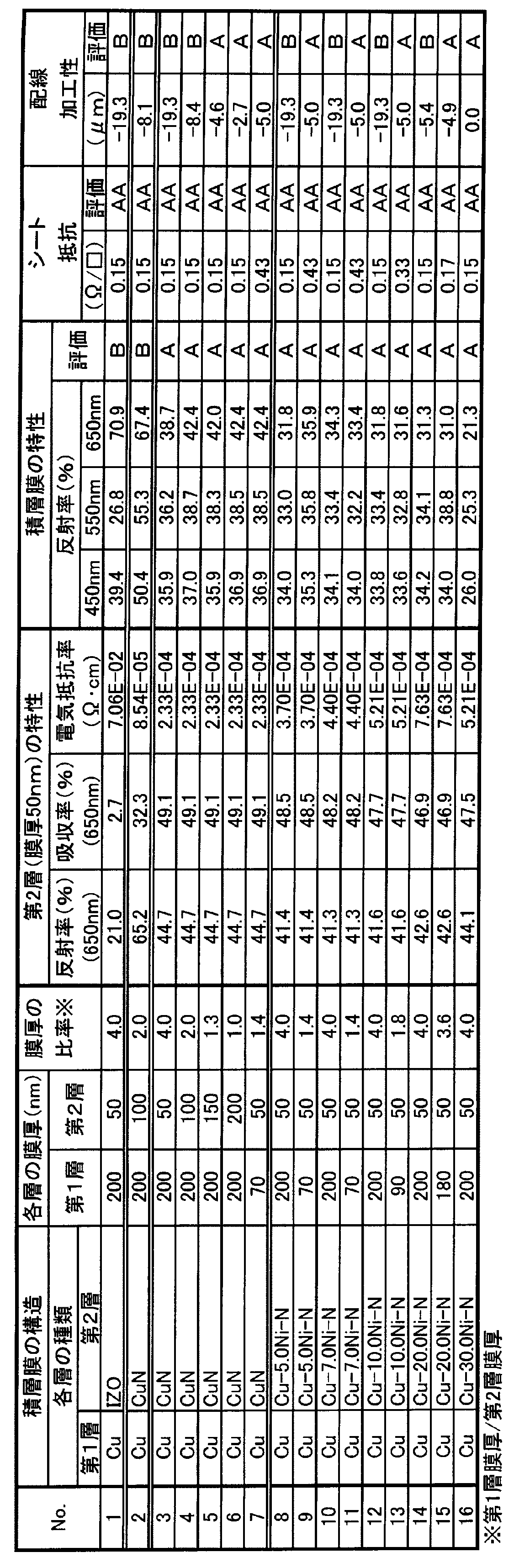

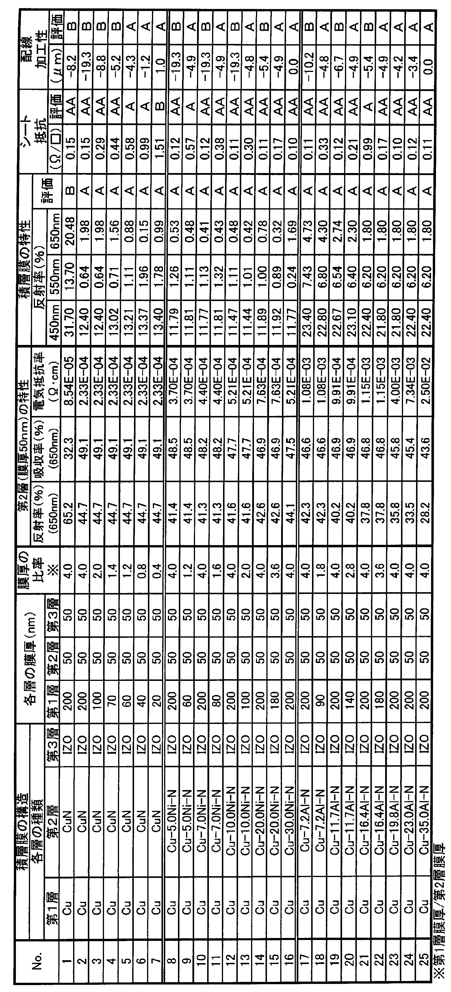

まず表2および表3から次のことがわかる。表2および表3には、第1層、および該第1層の光が入射する側に第2層を形成した2層積層膜の特性を示している。
表2のNo.1は、第2層として、波長650nmの反射率は45%以下であるが、波長650nmの吸収率が40%を著しく下回るIZO膜を積層した例である。このIZO膜を含む積層膜の可視光反射率も高くなった。この様にNo.1の積層膜は、十分な分光特性を有しておらず、低反射導電膜や低反射配線として適さない。
表2のNo.2は、第2層として、波長650nmの反射率が45%超であってかつ波長650nmの吸収率が40%を下回るCuN膜を積層した例である。このNo.2では、第2層がCuN膜であるが十分な分光特性を示さないため、このCuN膜を含む積層膜は可視光反射率が高くなり、低反射導電膜や低反射配線として適さない。
表2のNo.3~7は、第2層として、波長650nmの反射率が45%以下であって吸収率が40%以上のCuN膜を積層した例である。この様に十分な分光特性を有する第2層を含むNo.3~7の積層膜は、いずれも可視光反射率が低く、かつシート抵抗も小さく、低反射導電膜として適している。尚、No.2とNo.4は、第2層の成分と膜厚が同じで光学特性が異なっているが、これは、第2層の形成時のガス圧が両者で異なっているためである。
上記No.3~7のうち、No.3および4とNo.5~7との対比から、優れた配線加工性も兼備し、低反射配線としても有用な積層膜を得るには、第1層膜厚/第2層膜厚も制御するのがよく、具体的には、該第1層膜厚/第2層膜厚を1.4以下とすることが好ましく、より好ましくは1.0以下であることがわかる。
表2のNo.8~16は、第2層として、波長650nmの反射率が45%以下であって吸収率が40%以上のCu-Ni-N膜を積層した例である。この様に十分な分光特性を有する第2層を含むNo.8~16の積層膜は、いずれも可視光反射率が低く、かつシート抵抗も小さく、低反射導電膜として適している。
上記No.8~16のうち、No.8、10、12および14と、No.9、11、13および15との対比から、優れた配線加工性も兼備し低反射配線としても有用な積層膜を得るには、第1層膜厚/第2層膜厚または成分組成を制御するのがよいことがわかる。即ち、前述の図1と上記対比から、優れた配線加工性を確保するには、第1層膜厚/第2層膜厚を、Ni量が5.0原子%の場合は1.4以下とするのがよく、Ni量が7.0原子%の場合は1.4以下、Ni量が10.0原子%の場合は1.8以下、Ni量が20.0原子%の場合は3.6以下とするのがよいことがわかる。尚、第1層と第2層の膜厚許容範囲を広げる観点から、Ni量は5原子%以上であることが好ましく、より好ましくは10原子%以上である。
表3のNo.17~25は、第2層として、波長650nmの反射率が45%以下であって吸収率が40%以上のCu-Al-N膜を積層した例である。この様に十分な分光特性を有する第2層を含むNo.17~25の積層膜は、いずれも可視光反射率が低く、かつシート抵抗も小さく、低反射導電膜として適している。
上記No.17~25のうち、No.17、19および21と、No.18、20および22との対比から、優れた配線加工性も兼備し低反射配線としても有用な積層膜を得るには、第1層膜厚/第2層膜厚または成分組成を制御するのがよいことがわかる。即ち、前述の図2と上記対比から、優れた配線加工性を確保するには、第1層膜厚/第2層膜厚を、Al量が7.2原子%の場合は2.0以下とするのがよく、Al量が11.7原子%の場合は3.0以下、Al量が16.4原子%の場合は3.6以下とするのがよいことがわかる。尚、第1層と第2層の膜厚許容範囲を広げる観点から、Al量は3原子%以上とすることが好ましく、より好ましくは7原子%以上、さらに好ましくは15原子%以上である。
表3のNo.26~34は、第2層として、波長650nmの反射率が45%以下であって吸収率が40%以上のCu-Ni-Al-N膜を積層した例である。この様に十分な分光特性を有する第2層を含むNo.26~34の積層膜は、いずれも可視光反射率が低く、かつシート抵抗も小さく、低反射導電膜として適している。またNo.26~34の積層膜は、配線加工性にも優れており、低反射配線としても有用である。上記の通りNiとAlを共に含有させることによってエッチングレートが遅くなり、配線加工性が改善したものと考えられる。
表3のNo.35および36は、第1層にAl膜またはAg膜を用いた例を示している。第2層が本発明で規定の膜であれば、第1層にAl膜またはAg膜を用いても、得られる積層膜は低反射導電膜として求められる特性を満たすことがわかる。
次に表4および表5について考察する。表4および表5には、第1層、および該第1層の光が入射する側に第2層、第3層を順に形成した3層積層膜の特性を示している。
表4のNo.1は、第2層として、波長650nmの反射率が45%超であってかつ波長650nmの吸収率が40%を下回るCuN膜を積層した例である。このNo.1では、第2層がCuN膜であるが十分な分光特性を示さないため、このCuN膜を含む積層膜は可視光反射率が高くなり、低反射導電膜や低反射配線として適さない。
表4のNo.2~7は、第2層として、波長650nmの反射率が45%以下であって吸収率が40%以上のCuN膜を積層した例である。この様に十分な分光特性を有する第2層を含むNo.2~6の積層膜は、いずれも可視光反射率が低くかつシート抵抗も小さく低反射導電膜として適している。No.7は第1層の膜厚が薄いため、シート抵抗が高くなった。尚、積層膜のシート抵抗を十分小さくするには、第1層の膜厚を例えば70nm以上とすることが挙げられる。
表4のNo.2~6のうち、No.2~4とNo.5、6との対比から、優れた配線加工性も兼備し、低反射配線としても有用な積層膜を得るには、第1層膜厚/第2層膜厚も制御するのがよく、具体的には、該第1層膜厚/第2層膜厚を1.3以下とすることが好ましく、より好ましくは1.0以下であることがわかる。
表4のNo.8~16は、第2層として、波長650nmの反射率が45%以下であって吸収率が40%以上のCu-Ni-N膜を積層した例である。この様に十分な分光特性を有する第2層を含むNo.8~16の積層膜は、いずれも可視光反射率が低く、かつシート抵抗も小さく、低反射導電膜として適している。
上記No.8~16のうち、No.8、10、12および14と、No.9、11、13および15との対比から、優れた配線加工性も兼備し低反射配線としても有用な積層膜を得るには、第1層膜厚/第2層膜厚または成分組成を制御するのがよいことがわかる。即ち、上記対比から、優れた配線加工性を確保するには、第1層膜厚/第2層膜厚を、Ni量が5.0原子%の場合は1.2以下とするのがよく、Ni量が7.0原子%の場合は1.6以下、Ni量が10.0原子%の場合は2.0以下、Ni量が20.0原子%の場合は3.6以下とするのがよいことがわかる。尚、第1層と第2層の膜厚許容範囲を広げる観点から、Ni量は5原子%以上であることが好ましく、より好ましくは10原子%以上である。
表4のNo.17~25は、第2層として、波長650nmの反射率が45%以下であって吸収率が40%以上のCu-Al-N膜を積層した例である。この様に十分な分光特性を有する第2層を含むNo.17~25の積層膜は、いずれも可視光反射率が低く、かつシート抵抗も小さく、低反射導電膜として適している。
上記No.17~25のうち、No.17、19および21と、No.18、20および22との対比から、優れた配線加工性も兼備し低反射配線としても有用な積層膜を得るには、第1層膜厚/第2層膜厚または成分組成を制御するのがよいことがわかる。即ち、上記対比から、優れた配線加工性を確保するには、第1層膜厚/第2層膜厚を、Al量が7.2原子%の場合は約1.8以下とするのがよく、Al量が11.7原子%の場合は2.8以下、Al量が16.4原子%の場合は3.6以下とするのがよいことがわかる。尚、第1層と第2層の膜厚許容範囲を十分に広げる観点から、Al量は7原子%以上とすることが好ましく、より好ましくは15原子%以上である。
表5のNo.26~34は、第2層として、波長650nmの反射率が45%以下であって吸収率が40%以上のCu-Ni-Al-N膜を積層した例である。この様に十分な分光特性を有する第2層を含むNo.26~34の積層膜は、いずれも可視光反射率が低く、かつシート抵抗も小さく、低反射導電膜として適している。またNo.26~34の積層膜は、配線加工性にも優れており、低反射配線としても有用である。前述の通りNiとAlを共に含有させることによってエッチングレートが遅くなり、配線加工性が改善したものと考えられる。
表5のNo.35~46は、第1層に種々のCu合金膜を用いた例を示している。第2層として本発明で規定の膜を積層させることにより、第1層として表5に示すいずれの合金組成のCu合金膜を用いても、積層膜に要求される、優れた光学特性、低いシート抵抗および優れた配線加工性の全てを満足することがわかる。
表5のNo.47および48は、第1層にAl膜またはAg膜を用いた例を示している。第2層が本発明で規定の膜であれば、第1層にAl膜またはAg膜を用いても、得られる積層膜は低反射導電膜として要求される特性を満たすことがわかる。
表5のNo.49~52は、光学調整層として作用する第3層を、ITO膜、ZnO膜、ZTO膜、またはZAO膜とした例である。このNo.49~52の結果から、上記いずれの酸化物膜を積層させた場合であっても、積層膜に要求される、優れた光学特性、低いシート抵抗および優れた配線加工性の全てを満足することがわかる。
1 液晶表示装置
2 TFT基板
3 対向基板
4 カラーフィルタ基板
5A、5B、5C カラーフィルタ
6 ブラックマトリックス
7 液晶層
8 液晶封止材
10 入力装置
11 第1の金属電極、駆動用電極
12 第2の金属電極、検出用電極
13 絶縁層
13A 第1の絶縁層
13B 第2の絶縁層
14 カバーガラス
15 バックライト
30 入力装置
31A 第1の電極パターン
31B 第1のブリッジ電極
31C 第1の電極の外周配線
32A 第2の電極パターン
32B 第2のブリッジ電極
32C 第2の電極の外周配線
33 透明基板
41 カバーガラス
44 接着層
50、51 断面構造
52A 第1の透明電極
52B 第1のブリッジ電極
53 第2の透明電極
54 絶縁層
61 第1層
62 第2層
63 第3層
64 基板
65 密着層
66 第1層の端部
67 第2層の端部
Claims (17)
- NiとAlから選択される少なくとも1種のX元素を含み、残部がCuおよび不可避不純物であり、膜の一部が窒化し、かつ
膜厚が50nmである場合の、波長650nmの反射率が45%以下であると共に、波長650nmの光吸収率が40%以上であることを特徴とする窒素含有Cu合金膜。 - 第1層として、Ag、Al、Cu、またはこれらを基とする合金のいずれかからなり、かつ電気抵抗率が1.0×10⁻⁵Ω・cm以下である膜と、
第2層として、膜厚50nmにおける波長650nmの反射率が45%以下であって、波長650nmの光吸収率が40%以上である、膜の一部が窒化したCu膜とを有し、かつ
前記第1層と前記第2層の2層積層膜の可視光反射率が45%以下であると共に、該2層積層膜のシート抵抗が1.0Ω/□以下であることを特徴とする積層膜。 - 第1層として、Ag、Al、Cu、またはこれらを基とする合金のいずれかからなり、かつ電気抵抗率が1.0×10⁻⁵Ω・cm以下である膜と、
第2層として、膜厚50nmにおける波長650nmの反射率が45%以下であって、波長650nmの光吸収率が40%以上である、膜の一部が窒化したCu膜と、
第3層として、In、Zn、SnおよびAlよりなる群から選択される少なくとも1種の元素を含む酸化物膜とを有し、かつ
前記第1層、前記第2層および前記第3層の3層積層膜の可視光反射率が30%以下であると共に、該3層積層膜のシート抵抗が1.0Ω/□以下であることを特徴とする積層膜。 - 第1層として、Ag、Al、Cu、またはこれらを基とする合金のいずれかからなり、かつ電気抵抗率が1.0×10⁻⁵Ω・cm以下である膜と、
第2層として、請求項1に記載の窒素含有Cu合金膜とを有し、かつ
前記第1層と前記第2層の2層積層膜の可視光反射率が45%以下であると共に、該2層積層膜のシート抵抗が1.0Ω/□以下であることを特徴とする積層膜。 - 第1層として、Ag、Al、Cu、またはこれらを基とする合金のいずれかからなり、かつ電気抵抗率が1.0×10⁻⁵Ω・cm以下である膜と、
第2層として、請求項1に記載の窒素含有Cu合金膜と、
第3層として、In、Zn、SnおよびAlよりなる群から選択される少なくとも1種の元素を含む酸化物膜とを有し、かつ
前記第1層、前記第2層および前記第3層の3層積層膜の可視光反射率が30%以下であると共に、該3層積層膜のシート抵抗が1.0Ω/□以下であることを特徴とする積層膜。 - 前記第1層は、Mn、Ni、Co、Ge、ZnおよびTiよりなる群から選択される少なくとも1種のZ元素を含むCu合金膜である請求項2~5のいずれかに記載の積層膜。
- 前記第3層は、少なくともInを含む酸化物膜である請求項3または5に記載の積層膜。
- 前記第1層は、Mn、Ni、Co、Ge、ZnおよびTiよりなる群から選択される少なくとも1種のZ元素を含むCu合金膜であり、かつ前記第3層は、少なくともInを含む酸化物膜である請求項3または5に記載の積層膜。
- 前記第1層の膜厚は40~400nmである請求項2~5のいずれかに記載の積層膜。
- 請求項1に記載の窒素含有Cu合金膜を有する表示装置。
- 請求項2~5のいずれかに記載の積層膜を有する表示装置。
- 請求項1に記載の窒素含有Cu合金膜を有するタッチパネルセンサー。
- 請求項2~5のいずれかに記載の積層膜を有するタッチパネルセンサー。
- 請求項1に記載の窒素含有Cu合金膜を有する電磁波シールド。
- 請求項2~5のいずれかに記載の積層膜を有する電磁波シールド。
- 請求項1に記載の窒素含有Cu合金膜を形成するためのCu合金スパッタリングターゲット。
- 請求項1~5のいずれかに記載の窒素含有Cu合金膜または積層膜を製造する方法であって、前記窒素含有Cu合金膜または前記膜の一部が窒化したCu膜を、窒素ガスまたは窒素含有ガスを含む雰囲気下で反応性スパッタリング法により形成することを特徴とする窒素含有Cu合金膜または積層膜の製造方法。
Applications Claiming Priority (2)
| Application Number | Priority Date | Filing Date | Title |
|---|---|---|---|
| JP2015-069999 | 2015-03-30 | ||
| JP2015069999A JP2016191967A (ja) | 2015-03-30 | 2015-03-30 | 窒素含有Cu合金膜、積層膜、およびこれらの製造方法、ならびにCu合金スパッタリングターゲット |
Publications (1)
| Publication Number | Publication Date |
|---|---|
| WO2016158181A1 true WO2016158181A1 (ja) | 2016-10-06 |
Family
ID=57005605
Family Applications (1)
| Application Number | Title | Priority Date | Filing Date |
|---|---|---|---|
| PCT/JP2016/056491 Ceased WO2016158181A1 (ja) | 2015-03-30 | 2016-03-02 | 窒素含有Cu合金膜、積層膜、およびこれらの製造方法、ならびにCu合金スパッタリングターゲット |
Country Status (3)
| Country | Link |
|---|---|
| JP (1) | JP2016191967A (ja) |
| TW (1) | TW201641699A (ja) |
| WO (1) | WO2016158181A1 (ja) |
Cited By (3)
| Publication number | Priority date | Publication date | Assignee | Title |
|---|---|---|---|---|
| CN109504942A (zh) * | 2019-01-18 | 2019-03-22 | 黄饶 | 一种金属膜层表面超低反射率的加工工艺 |
| CN113481467A (zh) * | 2021-06-01 | 2021-10-08 | 北京科技大学 | 抑制Al-Ni纳米多层膜相变过程有序金属间化合物生成的方法 |
| CN114309586A (zh) * | 2021-12-31 | 2022-04-12 | 西安稀有金属材料研究院有限公司 | 一种高熵合金/炭黑复合电磁吸波材料及其制备方法 |
Families Citing this family (1)
| Publication number | Priority date | Publication date | Assignee | Title |
|---|---|---|---|---|
| JP7339016B2 (ja) * | 2019-04-24 | 2023-09-05 | 株式会社アルバック | 表示装置、配線膜、配線膜製造方法 |
Citations (3)
| Publication number | Priority date | Publication date | Assignee | Title |
|---|---|---|---|---|
| JP2010206062A (ja) * | 2009-03-05 | 2010-09-16 | Toray Ind Inc | 導電性フィルムおよびディスプレイ用フィルター |
| WO2014035196A1 (ko) * | 2012-08-31 | 2014-03-06 | 주식회사 엘지화학 | 금속 구조체 및 이의 제조방법 |
| KR20150029561A (ko) * | 2013-09-10 | 2015-03-18 | 히타치 긴조쿠 가부시키가이샤 | 적층 배선막 및 그 제조 방법 및 Ni 합금 스퍼터링 타깃재 |
Family Cites Families (2)
| Publication number | Priority date | Publication date | Assignee | Title |
|---|---|---|---|---|
| JP5938290B2 (ja) * | 2012-07-31 | 2016-06-22 | 小川 倉一 | 透明導電膜及びその製造方法 |
| JP2015007263A (ja) * | 2013-06-24 | 2015-01-15 | 株式会社日立ハイテクノロジーズ | 有機デバイス製造装置および有機デバイスの製造方法 |
-
2015
- 2015-03-30 JP JP2015069999A patent/JP2016191967A/ja active Pending
-
2016
- 2016-03-02 WO PCT/JP2016/056491 patent/WO2016158181A1/ja not_active Ceased
- 2016-03-17 TW TW105108227A patent/TW201641699A/zh unknown
Patent Citations (3)
| Publication number | Priority date | Publication date | Assignee | Title |
|---|---|---|---|---|
| JP2010206062A (ja) * | 2009-03-05 | 2010-09-16 | Toray Ind Inc | 導電性フィルムおよびディスプレイ用フィルター |
| WO2014035196A1 (ko) * | 2012-08-31 | 2014-03-06 | 주식회사 엘지화학 | 금속 구조체 및 이의 제조방법 |
| KR20150029561A (ko) * | 2013-09-10 | 2015-03-18 | 히타치 긴조쿠 가부시키가이샤 | 적층 배선막 및 그 제조 방법 및 Ni 합금 스퍼터링 타깃재 |
Cited By (5)
| Publication number | Priority date | Publication date | Assignee | Title |
|---|---|---|---|---|
| CN109504942A (zh) * | 2019-01-18 | 2019-03-22 | 黄饶 | 一种金属膜层表面超低反射率的加工工艺 |
| CN113481467A (zh) * | 2021-06-01 | 2021-10-08 | 北京科技大学 | 抑制Al-Ni纳米多层膜相变过程有序金属间化合物生成的方法 |
| CN113481467B (zh) * | 2021-06-01 | 2022-07-22 | 北京科技大学 | 抑制Al-Ni纳米多层膜相变过程有序金属间化合物生成的方法 |
| CN114309586A (zh) * | 2021-12-31 | 2022-04-12 | 西安稀有金属材料研究院有限公司 | 一种高熵合金/炭黑复合电磁吸波材料及其制备方法 |
| CN114309586B (zh) * | 2021-12-31 | 2024-01-26 | 西安稀有金属材料研究院有限公司 | 一种高熵合金/炭黑复合电磁吸波材料及其制备方法 |
Also Published As
| Publication number | Publication date |
|---|---|
| TW201641699A (zh) | 2016-12-01 |
| JP2016191967A (ja) | 2016-11-10 |
Similar Documents
| Publication | Publication Date | Title |
|---|---|---|
| TWI536403B (zh) | 導電結構體及其製造方法 | |
| CN103168285B (zh) | 包括导电图形的触摸面板及其制备方法 | |
| KR101656581B1 (ko) | 전도성 구조체 및 이의 제조방법 | |
| TWI567237B (zh) | 電極及其製造方法 | |
| WO2017016237A1 (en) | Conductive layer in a semiconductor apparatus, display substrate and display apparatus having the same, and fabricating method thereof | |
| WO2017212970A1 (ja) | 積層膜、表示装置及び入力装置 | |
| CN104838344B (zh) | 触摸面板、触摸面板的制造方法、光学薄膜基板及其制造方法 | |
| KR101987263B1 (ko) | 전도성 구조체 및 이의 제조방법 | |
| CN106662950A (zh) | 导电结构及其制造方法 | |
| WO2016158181A1 (ja) | 窒素含有Cu合金膜、積層膜、およびこれらの製造方法、ならびにCu合金スパッタリングターゲット | |
| KR101847751B1 (ko) | 입력 장치에 사용되는 전극, 및 그 제조 방법 | |
| JP6190792B2 (ja) | 電極およびその製造方法 | |
| CN107197627A (zh) | 导电结构体及其制造方法 | |
| CN111240507A (zh) | 导电性薄膜和其图案化方法 | |
| JP6228530B2 (ja) | 電極およびその製造方法 | |
| JP7326918B2 (ja) | 積層体 | |
| TWI647599B (zh) | 觸控面板、觸控面板之製造方法、顯示裝置及顯示裝置之製造方法 | |
| JP2019098565A (ja) | 積層体 | |
| CN110872687B (zh) | 层叠体及靶材 | |
| JP6157424B2 (ja) | 電極およびその製造方法 | |
| JP2017068219A (ja) | 電極構造 |
Legal Events
| Date | Code | Title | Description |
|---|---|---|---|
| 121 | Ep: the epo has been informed by wipo that ep was designated in this application |
Ref document number: 16772065 Country of ref document: EP Kind code of ref document: A1 |
|
| NENP | Non-entry into the national phase |
Ref country code: DE |
|
| 122 | Ep: pct application non-entry in european phase |
Ref document number: 16772065 Country of ref document: EP Kind code of ref document: A1 |