WO2016152390A1 - キャリア付極薄銅箔、その製造方法、銅張積層板及びプリント配線板 - Google Patents
キャリア付極薄銅箔、その製造方法、銅張積層板及びプリント配線板 Download PDFInfo
- Publication number
- WO2016152390A1 WO2016152390A1 PCT/JP2016/056014 JP2016056014W WO2016152390A1 WO 2016152390 A1 WO2016152390 A1 WO 2016152390A1 JP 2016056014 W JP2016056014 W JP 2016056014W WO 2016152390 A1 WO2016152390 A1 WO 2016152390A1
- Authority
- WO
- WIPO (PCT)
- Prior art keywords
- copper foil
- carrier
- ultrathin copper
- foil
- ultra
- Prior art date
- Legal status (The legal status is an assumption and is not a legal conclusion. Google has not performed a legal analysis and makes no representation as to the accuracy of the status listed.)
- Ceased
Links
Images
Classifications
-
- B—PERFORMING OPERATIONS; TRANSPORTING
- B32—LAYERED PRODUCTS
- B32B—LAYERED PRODUCTS, i.e. PRODUCTS BUILT-UP OF STRATA OF FLAT OR NON-FLAT, e.g. CELLULAR OR HONEYCOMB, FORM
- B32B7/00—Layered products characterised by the relation between layers; Layered products characterised by the relative orientation of features between layers, or by the relative values of a measurable parameter between layers, i.e. products comprising layers having different physical, chemical or physicochemical properties; Layered products characterised by the interconnection of layers
- B32B7/02—Physical, chemical or physicochemical properties
-
- B—PERFORMING OPERATIONS; TRANSPORTING
- B32—LAYERED PRODUCTS
- B32B—LAYERED PRODUCTS, i.e. PRODUCTS BUILT-UP OF STRATA OF FLAT OR NON-FLAT, e.g. CELLULAR OR HONEYCOMB, FORM
- B32B15/00—Layered products comprising a layer of metal
- B32B15/01—Layered products comprising a layer of metal all layers being exclusively metallic
-
- B—PERFORMING OPERATIONS; TRANSPORTING
- B32—LAYERED PRODUCTS
- B32B—LAYERED PRODUCTS, i.e. PRODUCTS BUILT-UP OF STRATA OF FLAT OR NON-FLAT, e.g. CELLULAR OR HONEYCOMB, FORM
- B32B15/00—Layered products comprising a layer of metal
- B32B15/04—Layered products comprising a layer of metal comprising metal as the main or only constituent of a layer, which is next to another layer of the same or of a different material
- B32B15/08—Layered products comprising a layer of metal comprising metal as the main or only constituent of a layer, which is next to another layer of the same or of a different material of synthetic resin
-
- B—PERFORMING OPERATIONS; TRANSPORTING
- B32—LAYERED PRODUCTS
- B32B—LAYERED PRODUCTS, i.e. PRODUCTS BUILT-UP OF STRATA OF FLAT OR NON-FLAT, e.g. CELLULAR OR HONEYCOMB, FORM
- B32B15/00—Layered products comprising a layer of metal
- B32B15/20—Layered products comprising a layer of metal comprising aluminium or copper
-
- H—ELECTRICITY
- H05—ELECTRIC TECHNIQUES NOT OTHERWISE PROVIDED FOR
- H05K—PRINTED CIRCUITS; CASINGS OR CONSTRUCTIONAL DETAILS OF ELECTRIC APPARATUS; MANUFACTURE OF ASSEMBLAGES OF ELECTRICAL COMPONENTS
- H05K1/00—Printed circuits
- H05K1/02—Details
- H05K1/09—Use of materials for the conductive, e.g. metallic pattern
-
- B—PERFORMING OPERATIONS; TRANSPORTING
- B32—LAYERED PRODUCTS
- B32B—LAYERED PRODUCTS, i.e. PRODUCTS BUILT-UP OF STRATA OF FLAT OR NON-FLAT, e.g. CELLULAR OR HONEYCOMB, FORM
- B32B2457/00—Electrical equipment
- B32B2457/08—PCBs, i.e. printed circuit boards
Definitions
- the present invention relates to an ultrathin copper foil with a carrier, a manufacturing method thereof, a copper clad laminate, and a printed wiring board.
- the subtractive method has been widely adopted as a method for manufacturing a printed wiring board.
- the subtractive method is a technique capable of forming a fine circuit using a copper foil.
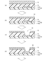
- the roughened surface of the copper foil 10 is bonded to the insulating resin substrate 12 having the lower layer circuit 12b on the base substrate 12a through the prepreg 14 (step (a)).
- step (b) the roughened surface of the copper foil 10 is bonded to the insulating resin substrate 12 having the lower layer circuit 12b on the base substrate 12a through the prepreg 14
- via holes 16 are formed by laser drilling (step (c)).
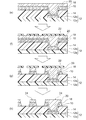
- step (d) chemical copper plating 18 (step (d)) and electrolytic copper plating 20 (step (e)) are performed, masking with a predetermined pattern by exposure and development using the dry film 22 (step (f)), and etching. Then, unnecessary copper foil or the like immediately below the opening of the dry film 22 is dissolved and removed (step (g)), and then the dry film 22 is peeled off (step (h)) to form the wiring 24 formed in a predetermined pattern. obtain.
- Patent Document 1 Japanese Patent Laid-Open No. 2001-326467 discloses a method for manufacturing a printed wiring board including forming a recess such as a via hole in a copper-clad laminate, and the outer layer of the copper-clad laminate is disclosed. It is disclosed that by adopting a corrugated copper foil as the copper foil, direct laser drilling that simultaneously removes the copper foil and the base resin using a carbon dioxide gas laser is made possible.
- Patent Document 2 Japanese Patent Laid-Open No.
- the surface of the ultrathin copper foil is subjected to blackening treatment, and then the blackened surface is irradiated with a carbon dioxide laser to produce ultrathin copper.
- a method for perforating a foil and an insulating layer immediately below the foil is disclosed.
- Patent Document 1 Although the technique using the corrugated copper foil as disclosed in Patent Document 1 has high laser drilling workability, the fine circuit formability may be inferior, ensuring high laser drilling workability. However, it is desired to further improve the fine circuit formability.
- the blackening treatment disclosed in Patent Document 2 requires time and cost, and the yield can be reduced. Therefore, direct laser drilling is desirably performed on the surface of the ultrathin copper foil without performing the blackening treatment. It is convenient if you can.
- the present inventors now have an average distance (Peak Spacing) between the surface peaks of the surface on the peeling layer side of the ultrathin copper foil of 2.5 to 20.0 ⁇ m, and Surface profile where the core level difference Rk is 1.5 to 3.0 ⁇ m, and the maximum height difference Wmax of the waviness on the side opposite to the peel-off layer of the ultrathin copper foil is 4.0 ⁇ m or less.
- Peak Spacing an average distance between the surface peaks of the surface on the peeling layer side of the ultrathin copper foil of 2.5 to 20.0 ⁇ m, and Surface profile where the core level difference Rk is 1.5 to 3.0 ⁇ m, and the maximum height difference Wmax of the waviness on the side opposite to the peel-off layer of the ultrathin copper foil is 4.0 ⁇ m or less.
- an object of the present invention is to provide an ultrathin copper foil with a carrier capable of achieving both laser drilling workability and fine circuit formability in processing of a copper-clad laminate or manufacturing of a printed wiring board. .
- an ultrathin copper foil with a carrier comprising a carrier foil, a release layer and an ultrathin copper foil in this order
- the surface on the peeling layer side of the ultrathin copper foil has an average distance (Peak Spacing) between surface peaks of 2.5 to 20.0 ⁇ m and a core portion depth difference Rk of 1. 5 to 3.0 ⁇ m
- the surface of the ultrathin copper foil opposite to the release layer is provided with an ultrathin copper foil with a carrier having a maximum waviness difference Wmax of 4.0 ⁇ m or less.
- a method for producing an ultrathin copper foil with a carrier according to the above aspect, Prepare a carrier foil having a surface with an average valley spacing (Valley Spacing) of 2.5 to 20.0 ⁇ m and a core level difference (core roundness depth) Rk of 2.0 to 3.8 ⁇ m.
- Process Forming a release layer on the surface of the carrier foil; Forming an ultrathin copper foil on the release layer; A method is provided comprising.
- a copper clad laminate comprising the ultrathin copper foil with a carrier according to the above aspect.
- a method for manufacturing a printed wiring board wherein the printed wiring board is manufactured using the ultrathin copper foil with a carrier according to the above aspect.
- average peak-to-surface peak is the waveform data related to the peak after removing the waviness component from the information on the unevenness of the sample surface obtained using a three-dimensional surface structure analysis microscope. The average distance between peaks in the data extracted by filtering.
- the “valley spacing” is obtained by filtering the waveform data related to the valley after removing the undulation component from the information on the unevenness of the sample surface obtained using a three-dimensional surface structure analysis microscope. This is the average distance between valleys in the extracted data.
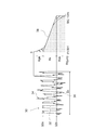
- the “core level difference Rk” is a parameter that can be determined in accordance with JIS B 0671-2: 2002, and as shown in FIG.
- the difference between the upper level 32a and the lower level 32b of the core portion (roughness core profile) 32 of this is the "core portion of the roughness curve” 30.
- the high protruding peak portion 34 and the deep protruding valley portion 36 are roughened.
- the “maximum waviness difference Wmax” is a waveform obtained by extracting waveform data relating to waviness using a filter from information relating to the unevenness of the sample surface obtained using a three-dimensional surface structure analysis microscope.
- the maximum value of the data height difference (the sum of the maximum peak height and the maximum valley depth of the waveform).
- ten-point average roughness Rzjis is a parameter that can be determined in accordance with JIS B 0601: 2001.
- the roughness curve of the reference length up to the fifth highest from the highest peak. This is the sum of the average of the mountain height and the average of the depth of the valleys from the deepest valley bottom to the fifth deepest.
- the average distance between surface peaks (Peak spacing), the average distance between valleys (Valley spacing), the core level difference (core roughness depth) Rk, the maximum height difference Wmax of waviness, and the ten-point average roughness Rzjis, Using a commercially available three-dimensional surface structure analysis microscope (for example, zygo New View 5032 (manufactured by Zygo)) and commercially available analysis software (for example, Metro Pro Ver. 8.0.2), the low frequency filter is set to a condition of 11 ⁇ m. Can be measured.
- the non-measurement surface of the foil was fixed in close contact with the sample stage, and measurement was performed by selecting 6 points of view of 108 ⁇ m ⁇ 144 ⁇ m within the 1 cm square range of the sample piece, and obtained from the 6 measurement points.
- the average value of the measured values obtained is preferably adopted as the representative value.
- the “electrode surface” of the carrier foil refers to the surface on the side in contact with the cathode when the carrier foil was produced.
- the “deposition surface” of the carrier foil refers to the surface on the side where electrolytic copper is deposited when the carrier foil is produced, that is, the surface not in contact with the cathode.
- the ultrathin copper foil with carrier of the present invention comprises a carrier foil, a release layer and an ultrathin copper foil in this order.
- the surface on the peeling layer side of the ultrathin copper foil has an average distance between peak peaks (Peak Spacing) of 2.5 to 20.0 ⁇ m, and a core portion level difference (core roundness depth) Rk of 1 .5 to 3.0 ⁇ m.
- the surface of the ultrathin copper foil opposite to the release layer has a maximum waviness difference Wmax of 4.0 ⁇ m or less.
- ultrathin copper foil is difficult to achieve both laser drilling workability and fine circuit formability unless blackening treatment is performed. However, according to the present invention, both can be achieved unexpectedly.
- an ultrathin copper foil having a smooth surface opposite to the peeling layer is required.
- an ultrathin copper foil having a smooth surface on the peeling layer side is required.
- the smoother the surface the more easily the laser is reflected. This is because it becomes difficult to be absorbed by the thin copper foil and the laser drilling processability is lowered.
- the technique using the corrugated copper foil as disclosed in Patent Document 1 has high laser drilling workability, but may be inferior in microcircuit formability.
- the ultrathin copper foil with a carrier of the present invention it is possible to improve the fine circuit formability while ensuring high laser drilling workability.
- Such compatibility between laser drilling workability and fine circuit formability is considered to be realized as follows.
- the level difference Rk of the core portion on the surface of the peeling layer side of the ultrathin copper foil is 1.5 ⁇ m or more, and the average distance (Peak Spacing) between surface peaks on the surface of the peeling layer side of the ultrathin copper foil By setting the thickness to 2.5 to 20.0 ⁇ m, it is considered that high direct laser drilling workability is realized.
- the level difference Rk of the core portion 32 is different from the ten-point average roughness Rzjis and is a curve obtained by removing the high protruding peak portion 34 and the deep protruding valley portion 36 from the roughness curve 30.
- the direct laser drilling processability is improved as a synergistic effect of the Rk control and the Peak Spacing control.
- the level difference Rk of the core portion on the surface of the peeling layer side of the ultrathin copper foil is set to 3.0 ⁇ m or less, and the maximum height difference Wmax of the undulation on the surface on the side opposite to the peeling layer of the ultrathin copper foil is set.
- the thickness is set to 4.0 ⁇ m or less, it is considered that an improvement in microcircuit formability is realized without impairing such high laser drilling workability.
- the present inventors have ascertained that the main factor that decreases the fine circuit formability is the undulation of the surface opposite to the peeling layer of the ultrathin copper foil, and the maximum difference in undulation (Wmax) is determined. It has been found that controlling to 4.0 ⁇ m or less contributes to improvement of microcircuit formation. In particular, 4.0 ⁇ m, which is the upper limit value of the maximum waviness difference Wmax, is not an extremely low value, and therefore, extreme smoothness is not required on the surface of the copper foil opposite to the release layer (typical) It can be said that the surface profile is particularly suitable for the subtractive method. However, the present invention may be applied to methods other than the subtractive method (for example, the MSAP (Modified Semi-Additive Process) method).
- MSAP Modem Semi-Additive Process
- the ultra-thin copper foil has an average distance between peak peaks (Peak Spacing) of 2.5 to 20.0 ⁇ m, and a core level difference (core roundness depth) Rk of 1.5 to 3
- a surface having a thickness of 0.0 ⁇ m is provided on the surface on the side of the release layer, and a surface having a maximum waviness difference Wmax of 4.0 ⁇ m or less is provided on the surface on the side opposite to the release layer.
- the average distance (Peak spacing) between surface peaks on the surface on the peeling layer side of the ultrathin copper foil is 2.5 to 20.0 ⁇ m, preferably 6.5 to 15.0 ⁇ m.
- the core level difference Rk on the surface of the ultrathin copper foil on the release layer side is 1.5 to 3.0 ⁇ m, preferably 2.0 to 3.0 ⁇ m.
- the maximum height difference Wmax of the undulation on the surface opposite to the peeling layer of the ultrathin copper foil is 4.0 ⁇ m or less, preferably 3.0 ⁇ m or less, more preferably 2.5 ⁇ m or less.
- Wmax on the surface of the ultrathin copper foil is 3.0 ⁇ m or less. Since Wmax is preferably as low as possible, the lower limit is not particularly limited, but Wmax is typically 0.1 ⁇ m or more, and more typically 0.2 ⁇ m or more.
- the surface on the peeling layer side of the ultrathin copper foil has a ten-point average roughness Rzjis of preferably 2.0 to 4.0 ⁇ m, more preferably 2.5 to 4.0 ⁇ m. Within such a range, it contributes to improving the balance between laser drilling workability and fine circuit formability.
- the surface of the ultrathin copper foil opposite to the release layer has a ten-point average roughness Rzjis of preferably 4.0 ⁇ m or less, more preferably 3.0 ⁇ m or less, and even more preferably 2.5 ⁇ m or less. Within this range, it contributes to the improvement of fine circuit formability.
- the ten-point average roughness Rzjis is typically 0.5 ⁇ m or more and more typically 1.0 ⁇ m or more from the viewpoint of adhesion to the resin layer.
- the surface of the ultrathin copper foil opposite to the release layer is preferably a roughened surface. That is, it is preferable that one surface of the ultrathin copper foil is roughened.
- This roughening treatment passes through at least two types of plating processes including a baking plating process for depositing fine copper particles on an ultrathin copper foil and a covering plating process for preventing the fine copper grains from falling off. It is preferable to carry out according to a known plating technique.
- the surface of the ultrathin copper foil opposite to the release layer is a roughened surface, and more preferably satisfies the above-mentioned ten-point average roughness Rzjis.
- the ultra-thin copper foil may be a known configuration employed for the ultra-thin copper foil with a carrier, except that it has the above-mentioned specific surface profile, and is not particularly limited.
- the ultrathin copper foil may be formed by a wet film formation method such as an electroless copper plating method and an electrolytic copper plating method, a dry film formation method such as sputtering and chemical vapor deposition, or a combination thereof.
- the preferred thickness of the ultrathin copper foil is 0.5 to 5.0 ⁇ m.
- the thickness of the ultrathin copper foil is particularly preferably 3.0 ⁇ m or less.
- the release layer is a layer having a function of weakening the peeling strength of the carrier foil, ensuring the stability of the strength, and further suppressing interdiffusion that may occur between the carrier foil and the copper foil during press molding at a high temperature. It is.
- the release layer is generally formed on one side of the carrier foil, but may be formed on both sides.
- the release layer may be either an organic release layer or an inorganic release layer. Examples of organic components used in the organic release layer include nitrogen-containing organic compounds, sulfur-containing organic compounds, carboxylic acids and the like. Examples of nitrogen-containing organic compounds include triazole compounds, imidazole compounds, and the like. Among these, triazole compounds are preferred in terms of easy release stability.
- triazole compounds examples include 1,2,3-benzotriazole, carboxybenzotriazole, N ′, N′-bis (benzotriazolylmethyl) urea, 1H-1,2,4-triazole and 3-amino- And 1H-1,2,4-triazole.
- sulfur-containing organic compound examples include mercaptobenzothiazole, thiocyanuric acid, 2-benzimidazolethiol and the like.
- carboxylic acid examples include monocarboxylic acid and dicarboxylic acid.
- examples of inorganic components used in the inorganic release layer include Ni, Mo, Co, Cr, Fe, Ti, W, P, Zn, and a chromate-treated film.
- the release layer may be formed by bringing a release layer component-containing solution into contact with at least one surface of the carrier foil and fixing the release layer component to the surface of the carrier foil.
- this contact may be performed by immersion in the release layer component-containing solution, spraying of the release layer component-containing solution, flowing down of the release layer component-containing solution, or the like.
- the release layer component may be fixed to the surface of the carrier foil by adsorption or drying of the release layer component-containing solution, electrodeposition of the release layer component in the release layer component-containing solution, or the like.
- the thickness of the release layer is typically 1 nm to 1 ⁇ m, preferably 5 nm to 500 nm.
- the carrier foil is a foil for supporting an ultrathin copper foil and improving its handleability.
- the carrier foil include an aluminum foil, a copper foil, a stainless steel (SUS) foil, a resin film whose surface is metal-coated, and preferably a copper foil.
- the copper foil may be a rolled copper foil or an electrolytic copper foil.
- the thickness of the carrier foil is typically 250 ⁇ m or less, preferably 12 ⁇ m to 200 ⁇ m.
- the surface of the carrier foil on the release layer side has an average distance between valleys (Valley spacing) of 2.5 to 20.0 ⁇ m, and a core level difference (core roughness depth) Rk of 2.0 to 3.8 ⁇ m. Is preferred.
- valleys Peak spacing
- core roughness depth core roughness depth
- the ultra-thin copper foil with a carrier of the present invention has an average distance between valleys of 2.5 to 20.0 ⁇ m and a core level difference Rk of 2.0 to 2.0. It can be manufactured by preparing a carrier foil having a surface of 3.8 ⁇ m, forming a release layer on the surface of the carrier foil, and forming an ultrathin copper foil on the release layer.
- the surface on the release layer side of the carrier foil preferably has a ten-point average roughness Rzjis of 2.0 to 5.0 ⁇ m.
- the average distance (Valley spacing) between the valleys on the surface of the carrier foil on the release layer side is preferably 4.5 to 10.0 ⁇ m.
- Realization of Valley spacing, Rk, and Rzjis within the above range on the surface of the carrier foil is performed by treating the electrolytic solution (for example, sulfuric acid copper sulfate solution) with activated carbon to remove the residual additive in the electrolytic solution, and then after the activated carbon treatment.
- An additive such as glue or gelatin is newly added to the electrolytic solution and electrolysis is performed under known conditions to produce an electrolytic copper foil having a thickness of about 15 to 35 ⁇ m (for example, patent document). 3 (refer to the production method described in JP-A-9-241882).
- another functional layer may be provided between the release layer and the carrier foil and / or ultrathin copper foil.
- An example of such another functional layer is an auxiliary metal layer.
- the auxiliary metal layer is preferably made of nickel and / or cobalt. By forming such an auxiliary metal layer on the surface side of the carrier foil and / or on the surface side of the ultrathin copper foil, it may occur between the carrier foil and the ultrathin copper foil during hot press molding at a high temperature or for a long time. Interdiffusion can be suppressed and the stability of the peeling strength of the carrier foil can be ensured.
- the thickness of the auxiliary metal layer is preferably 0.001 to 3 ⁇ m.
- rust prevention treatment may be applied to the ultrathin copper foil.
- the rust prevention treatment preferably includes a plating treatment using zinc.
- the plating treatment using zinc may be either a zinc plating treatment or a zinc alloy plating treatment, and the zinc alloy plating treatment is particularly preferably a zinc-nickel alloy treatment.
- the zinc-nickel alloy treatment may be a plating treatment containing at least Ni and Zn, and may further contain other elements such as Sn, Cr, and Co.
- the Ni / Zn adhesion ratio in the zinc-nickel alloy plating is preferably 1.2 to 10, more preferably 2 to 7, and still more preferably 2.7 to 4 in terms of mass ratio.
- the rust prevention treatment preferably further includes a chromate treatment, and this chromate treatment is more preferably performed on the surface of the plating containing zinc after the plating treatment using zinc.
- rust prevention property can further be improved.
- a particularly preferable antirust treatment is a combination of a zinc-nickel alloy plating treatment and a subsequent chromate treatment.
- the surface of the ultrathin copper foil may be treated with a silane coupling agent to form a silane coupling agent layer.
- a silane coupling agent layer can be formed by appropriately diluting and applying a silane coupling agent and drying.
- silane coupling agents include epoxy-functional silane coupling agents such as 4-glycidylbutyltrimethoxysilane and ⁇ -glycidoxypropyltrimethoxysilane, or ⁇ -aminopropyltrimethoxysilane, N- ⁇ (amino Amino functions such as ethyl) ⁇ -aminopropyltrimethoxysilane, N-3- (4- (3-aminopropoxy) butoxy) propyl-3-aminopropyltrimethoxysilane, N-phenyl- ⁇ -aminopropyltrimethoxysilane Silane coupling agent, or mercapto functional silane coupling agent such as ⁇ -mercaptopropyltrimethoxysilane, or olefin functional silane coupling agent such as vinyltrimethoxysilane, vinylphenyltrimethoxysilane, or ⁇ -methacryloxypropyl Trimetoki Acrylic-functional silane coupling
- the ultrathin copper foil with a carrier of the present invention is preferably used for the production of a copper-clad laminate for printed wiring boards. That is, according to the preferable aspect of this invention, the copper clad laminated board obtained using the ultra-thin copper foil with a carrier is provided.
- This copper clad laminate comprises the ultrathin copper foil with a carrier of the present invention and a resin layer provided in close contact with the surface treatment layer.
- the ultra-thin copper foil with a carrier may be provided on one side of the resin layer or may be provided on both sides.
- the resin layer comprises a resin, preferably an insulating resin.
- the resin layer is preferably a prepreg and / or a resin sheet.
- the prepreg is a general term for composite materials in which a base material such as a synthetic resin plate, a glass plate, a glass woven fabric, a glass nonwoven fabric, and paper is impregnated with a synthetic resin.
- Preferable examples of the insulating resin include an epoxy resin, a cyanate resin, a bismaleimide triazine resin (BT resin), a polyphenylene ether resin, and a phenol resin.
- the insulating resin that constitutes the resin sheet include insulating resins such as epoxy resins, polyimide resins, and polyester resins.
- the filler particle etc. which consist of various inorganic particles, such as a silica and an alumina, may contain in the resin layer from a viewpoint of improving insulation.
- the thickness of the resin layer is not particularly limited, but is preferably 1 to 1000 ⁇ m, more preferably 2 to 400 ⁇ m, and still more preferably 3 to 200 ⁇ m.
- the resin layer may be composed of a plurality of layers.
- a resin layer such as a prepreg and / or a resin sheet may be provided on the ultrathin copper foil with a carrier via a primer resin layer previously applied to the surface of the copper foil.
- the ultrathin copper foil with a carrier of the present invention is preferably used for production of a printed wiring board. That is, according to the preferable aspect of this invention, the printed wiring board obtained using the ultra-thin copper foil with a carrier is provided.
- the printed wiring board according to this aspect includes a layer configuration in which a resin layer and a copper layer are laminated in this order.
- a copper layer is a layer originating in the ultra-thin copper foil of the ultra-thin copper foil with a carrier of this invention.
- the resin layer is as described above for the copper-clad laminate.
- the printed wiring board can employ a known layer configuration except that the ultrathin copper foil with a carrier of the present invention is used.
- Specific examples of the printed wiring board include a single-sided or double-sided printed wiring board formed with a circuit on the laminated body obtained by bonding the ultrathin copper foil of the present invention to one side or both sides of the prepreg, and a multilayer in which these are multilayered.
- a printed wiring board etc. are mentioned.
- Other specific examples include a flexible printed wiring board, a COF, a TAB tape, and the like that form a circuit by forming the ultrathin copper foil of the present invention on a resin film.
- examples thereof include an electronic material for glass, and an electromagnetic wave shielding film obtained by applying a conductive adhesive to the ultrathin copper foil of the present invention.
- the ultrathin copper foil with a carrier of the present invention is suitable for the subtractive method.
- a configuration as shown in FIGS. 1 and 2 can be employed.
- Example 1 After the release layer and the ultrathin copper foil layer were formed in this order on the deposition surface side of the carrier foil, an ultrathin copper foil with a carrier was prepared by performing a rust prevention treatment and a silane coupling agent treatment. And various evaluation was performed about the obtained ultra-thin copper foil with a carrier.
- the specific procedure is as follows.
- auxiliary metal layer Formation of auxiliary metal layer
- the carrier foil on which the organic peeling layer is formed is immersed in a solution containing nickel concentration of 20 g / L prepared using nickel sulfate, and the liquid temperature is 45 ° C., the pH is 3, and the current density is 5 A.
- nickel having a thickness equivalent to 0.001 ⁇ m was deposited on the organic release layer.
- a nickel layer was formed as an auxiliary metal layer on the organic release layer.
- Roughening treatment The surface of the ultrathin copper foil thus formed was subjected to a roughening treatment.
- This roughening treatment includes a baking plating process in which fine copper grains are deposited on an ultrathin copper foil, and a covering plating process for preventing the fine copper grains from falling off.
- a roughening treatment was performed at an acid density of 25 A / dm 2 using an acidic copper sulfate solution containing a copper concentration of 10 g / L and a sulfuric acid concentration of 120 g / L.
- electrodeposition was performed using an acidic copper sulfate solution containing a copper concentration of 70 g / L and a sulfuric acid concentration of 120 g / L under smooth plating conditions of a liquid temperature of 40 ° C. and a current density of 15 A / dm 2 .
- the surface of the roughening treatment layer of the obtained ultrathin copper foil with carrier was subjected to a rust prevention treatment comprising zinc-nickel alloy plating treatment and chromate treatment.
- the surface of the carrier foil was subjected to zinc-nickel alloy plating.
- a chromate treatment was performed on the surface that had been subjected to the zinc-nickel alloy plating treatment using an aqueous chromic acid concentration of 3 g / L under conditions of pH 10 and a current density of 5 A / dm 2 .
- Silane coupling agent treatment An aqueous solution with a concentration of 2 g / L of ⁇ -glycidoxypropyltrimethoxysilane is adsorbed on the surface of the ultrathin copper foil with a carrier and evaporated with an electric heater. Then, the silane coupling agent treatment was performed. At this time, the silane coupling agent treatment was not performed on the carrier foil side.
- ⁇ Surface property parameters> Zygo New View 5032 (manufactured by Zygo) was used as the measuring instrument, and Metro Pro Ver. 8.0.2, using a low frequency filter under the condition of 11 ⁇ m, the carrier foil and the ultrathin copper foil, the average distance between the surface peaks (Peak spacing), the average distance between the valleys (Valley spacing), The ten-point average roughness Rzjis, the core level difference Rk, and / or the maximum waviness difference Wmax were measured.
- an ultra-thin copper foil or carrier foil is fixed in close contact with the sample stage, and 6 fields of 108 ⁇ m ⁇ 144 ⁇ m are selected and measured within the 1 cm square range of the sample piece. The average value of the measured values obtained was adopted as a representative value.
- the surface at the side of the peeling layer of ultra-thin copper foil it measured after producing the copper-clad laminated board for laser drilling workability evaluation mentioned later.
- a copper-clad laminate was prepared using an ultrathin copper foil with a carrier, and laser drilling workability was evaluated.
- an ultrathin copper foil of a carrier-attached ultrathin copper foil is laminated on the surface of the inner layer substrate via a prepreg (manufactured by Mitsubishi Gas Chemical Co., Inc., 830NX-A, thickness 0.2 mm).
- the carrier foil was peeled off to produce a copper clad laminate.
- a carbon dioxide laser was used for the copper clad laminate, and a pulse width of 12 ⁇ sec.
- Laser drilling was performed under the conditions of a pulse energy of 8 mJ and a laser beam diameter of 97 ⁇ m.
- the diameters in the x direction and the y direction were measured for 10 holes formed by laser drilling, and the average value thereof was calculated as the hole diameter after processing.
- the hole diameter after processing became 70 ⁇ m or more, it was determined as A, 65 ⁇ m or more and less than 70 ⁇ m was determined as B, and less than 65 ⁇ m was determined as C.
- Example 2 Production and evaluation of an ultrathin copper foil with a carrier were carried out in the same manner as in Example 1 except that the ultrathin copper foil was formed by the following procedure.
- the carrier foil on which the auxiliary metal layer is formed is immersed in a bright plating solution having the following composition, electrolyzed at a solution temperature of 45 to 50 ° C. and a current density of 33 A / dm 2 , and an ultrathin copper foil having a thickness of 3 ⁇ m. Was formed on the auxiliary metal layer.
- Example 3 An ultrathin copper foil with a carrier was produced and evaluated in the same manner as in Example 2 except that a carrier foil having a thickness of 35 ⁇ m was produced.
- Example 4 (Comparison) An ultrathin copper foil with a carrier was produced and evaluated in the same manner as in Example 1 except that the carrier foil was produced according to the following procedure.
- a sulfuric acid copper sulfate solution having the following composition is used as the copper electrolyte, a titanium rotating electrode having a surface roughness Ra of 0.20 ⁇ m is used as the cathode, and a DSA (dimensionally stable anode) is used as the anode. Electrolysis was performed at a solution temperature of 50 ° C. and a current density of 60 A / dm 2 to obtain an electrolytic copper foil having a thickness of 35 ⁇ m as a carrier foil.
- Example 5 (Comparison) An ultrathin copper foil with a carrier was prepared and evaluated in the same manner as in Example 1 except that a carrier foil having a thickness of 35 ⁇ m was prepared.
Landscapes
- Engineering & Computer Science (AREA)
- Microelectronics & Electronic Packaging (AREA)
- Laminated Bodies (AREA)
- Electroplating Methods And Accessories (AREA)
- Parts Printed On Printed Circuit Boards (AREA)
- Production Of Multi-Layered Print Wiring Board (AREA)
Abstract
Description
前記極薄銅箔の剥離層側の面は、表面ピーク間の平均距離(Peak Spacing)が2.5~20.0μmであり、かつ、コア部のレベル差(core roughness depth)Rkが1.5~3.0μmであり、
前記極薄銅箔の剥離層と反対側の面は、うねりの最大高低差Wmaxが4.0μm以下である、キャリア付極薄銅箔が提供される。
谷間の平均距離(Valley Spacing)が2.5~20.0μmであり、かつ、コア部のレベル差(core roughness depth)Rkが2.0~3.8μmである表面を有するキャリア箔を用意する工程と、
前記キャリア箔の前記表面に剥離層を形成する工程と、
前記剥離層上に極薄銅箔を形成する工程と、
を含んでなる、方法が提供される。
本発明を特定するために用いられるパラメータの定義を以下に示す。
本発明のキャリア付極薄銅箔は、キャリア箔、剥離層及び極薄銅箔をこの順に備えてなる。そして、極薄銅箔の剥離層側の面は、表面ピーク間の平均距離(Peak Spacing)が2.5~20.0μmであり、かつ、コア部のレベル差(core roughness depth)Rkが1.5~3.0μmである。また、極薄銅箔の剥離層と反対側の面は、うねりの最大高低差Wmaxが4.0μm以下である。これにより、銅張積層板の加工ないしプリント配線板の製造において、レーザー穴開け加工性と微細回路形成性とを両立することが可能となる。しかも、レーザー穴開け加工性を確保するためにこれまで一般的に採用されている黒化処理を本発明においては不要にすることができる。
本発明のキャリア付極薄銅箔はプリント配線板用銅張積層板の作製に用いられるのが好ましい。すなわち、本発明の好ましい態様によれば、キャリア付極薄銅箔を用いて得られた銅張積層板が提供される。本発明のキャリア付極薄銅箔を用いることで、銅張積層板の加工において、レーザー穴開け加工性と微細回路形成性とを両立することができる。この銅張積層板は、本発明のキャリア付極薄銅箔と、該表面処理層に密着して設けられる樹脂層とを備えてなる。キャリア付極薄銅箔は樹脂層の片面に設けられてもよいし、両面に設けられてもよい。樹脂層は、樹脂、好ましくは絶縁性樹脂を含んでなる。樹脂層はプリプレグ及び/又は樹脂シートであるのが好ましい。プリプレグとは、合成樹脂板、ガラス板、ガラス織布、ガラス不織布、紙等の基材に合成樹脂を含浸させた複合材料の総称である。絶縁性樹脂の好ましい例としては、エポキシ樹脂、シアネート樹脂、ビスマレイミドトリアジン樹脂(BT樹脂)、ポリフェニレンエーテル樹脂、フェノール樹脂等が挙げられる。また、樹脂シートを構成する絶縁性樹脂の例としては、エポキシ樹脂、ポリイミド樹脂、ポリエステル樹脂等の絶縁樹脂が挙げられる。また、樹脂層には絶縁性を向上する等の観点からシリカ、アルミナ等の各種無機粒子からなるフィラー粒子等が含有されていてもよい。樹脂層の厚さは特に限定されないが、1~1000μmが好ましく、より好ましくは2~400μmであり、さらに好ましくは3~200μmである。樹脂層は複数の層で構成されていてよい。プリプレグ及び/又は樹脂シート等の樹脂層は予め銅箔表面に塗布されるプライマー樹脂層を介してキャリア付極薄銅箔に設けられていてもよい。
本発明のキャリア付極薄銅箔はプリント配線板の作製に用いられるのが好ましい。すなわち、本発明の好ましい態様によれば、キャリア付極薄銅箔を用いて得られたプリント配線板が提供される。本発明のキャリア付極薄銅箔を用いることで、プリント配線板の製造において、レーザー穴開け加工性と微細回路形成性とを両立することができる。本態様によるプリント配線板は、樹脂層と、銅層とがこの順に積層された層構成を含んでなる。銅層は本発明のキャリア付極薄銅箔の極薄銅箔に由来する層である。また、樹脂層については銅張積層板に関して上述したとおりである。いずれにしても、プリント配線板は、本発明のキャリア付極薄銅箔を用いること以外は、公知の層構成が採用可能である。プリント配線板に関する具体例としては、プリプレグの片面又は両面に本発明の極薄銅箔を接着させ硬化した積層体とした上で回路形成した片面又は両面プリント配線板や、これらを多層化した多層プリント配線板等が挙げられる。また、他の具体例としては、樹脂フィルム上に本発明の極薄銅箔を形成して回路を形成するフレキシブルプリント配線板、COF、TABテープ等も挙げられる。さらに他の具体例としては、本発明の極薄銅箔に上述の樹脂層を塗布した樹脂付銅箔(RCC)を形成し、樹脂層を絶縁接着材層として上述のプリント基板に積層した後、極薄銅箔を配線層の全部又は一部としてモディファイド・セミアディティブ(MSAP)法、サブトラクティブ法等の手法で回路を形成したビルドアップ配線板や、極薄銅箔を除去してセミアディティブ法で回路を形成したビルドアップ配線板、半導体集積回路上へ樹脂付銅箔の積層と回路形成を交互に繰り返すダイレクト・ビルドアップ・オン・ウェハー等が挙げられる。より発展的な具体例として、上記樹脂付銅箔を基材に積層し回路形成したアンテナ素子、接着剤層を介してガラスや樹脂フィルムに積層しパターンを形成したパネル・ディスプレイ用電子材料や窓ガラス用電子材料、本発明の極薄銅箔に導電性接着剤を塗布した電磁波シールド・フィルム等も挙げられる。特に、本発明のキャリア付極薄銅箔はサブトラクティブ法に適している。例えば、サブトラクティブ法により回路形成した場合には図1及び2に示されるような構成が採用可能である。
キャリア箔の析出面側に剥離層及び極薄銅箔層を順に形成した後、防錆処理及びシランカップリング剤処理を行うことで、キャリア付極薄銅箔を作製した。そして、得られたキャリア付極薄銅箔について各種評価を行った。具体的な手順は以下のとおりである。
陰極に算術平均粗さRa(JIS B 0601:2001に準拠)が0.20μmのチタン製の回転電極を用い、陽極にはDSA(寸法安定性陽極)を用いて、銅電解液として以下に示される組成の硫酸酸性硫酸銅溶液を活性炭処理した後、活性炭処理後の電解液中水溶性ゼラチンの濃度が5mg/Lとなるように添加し、溶液温度50℃、電流密度60A/dm2で電解し、厚さ18μmの電解銅箔をキャリア箔として得た。
<硫酸酸性硫酸銅溶液の組成>
‐ 銅濃度:85g/L
‐ 硫酸濃度:270g/L
‐ 塩素濃度:30mg/L
酸洗処理されたキャリア箔の析出面を、CBTA(カルボキシベンゾトリアゾール)濃度1g/L、硫酸濃度150g/L及び銅濃度10g/LのCBTA水溶液に、液温30℃で30秒間浸漬し、CBTA成分をキャリア箔の析出面に吸着させた。こうして、キャリア箔の析出面にCBTA層を有機剥離層として形成した。
有機剥離層が形成されたキャリア箔を、硫酸ニッケルを用いて作製されたニッケル濃度20g/Lを含む溶液に浸漬して、液温45℃、pH3、電流密度5A/dm2の条件で、厚さ0.001μm相当の付着量のニッケルを有機剥離層上に付着させた。こうして有機剥離層上にニッケル層を補助金属層として形成した。
補助金属層が形成されたキャリア箔を、以下に示される組成の銅溶液に浸漬して、溶液温度50℃、電流密度5~30A/dm2で電解し、厚さ3μmの極薄銅箔を補助金属層上に形成した。
<溶液の組成>
‐ 銅濃度:60g/L
‐ 硫酸濃度:200g/L
こうして形成された極薄銅箔の表面に粗化処理を行った。この粗化処理は、極薄銅箔の上に微細銅粒を析出付着させる焼けめっき工程と、この微細銅粒の脱落を防止するための被せめっき工程とから構成される。焼けめっき工程では、銅濃度10g/L及び硫酸濃度120g/Lを含む酸性硫酸銅溶液を用いて、液温25℃、電流密度15A/dm2で粗化処理を行った。その後の被せめっき工程では、銅濃度70g/L及び硫酸濃度120g/Lを含む酸性硫酸銅溶液を用いて、液温40℃及び電流密度15A/dm2の平滑めっき条件で電着を行った。
得られたキャリア付極薄銅箔の粗化処理層の表面に、亜鉛-ニッケル合金めっき処理及びクロメート処理からなる防錆処理を行った。まず、亜鉛濃度0.2g/L、ニッケル濃度2g/L及びピロリン酸カリウム濃度300g/Lの電解液を用い、液温40℃、電流密度0.5A/dm2の条件で、粗化処理層及びキャリア箔の表面に亜鉛-ニッケル合金めっき処理を行った。次いで、クロム酸濃度3g/L水溶液を用い、pH10、電流密度5A/dm2の条件で、亜鉛-ニッケル合金めっき処理を行った表面にクロメート処理を行った。
γ-グリシドキシプロピルトリメトキシシラン濃度2g/Lの水溶液をキャリア付極薄銅箔の極薄銅箔側の表面に吸着させ、電熱器により水分を蒸発させることにより、シランカップリング剤処理を行った。このとき、シランカップリング剤処理はキャリア箔側には行わなかった。
こうして得られたキャリア付極薄銅箔について、各種特性の評価を以下のとおり行った。
測定機器としてzygo New View 5032(Zygo社製)を用い、解析ソフトとしてMetro Pro Ver.8.0.2を用いて、低周波フィルタを11μmの条件を採用して、キャリア箔と極薄銅箔について、表面ピーク間の平均距離(Peak spacing)、谷間の平均距離(Valley spacing)、十点平均粗さRzjis、コア部のレベル差Rk、及び/又はうねりの最大高低差Wmaxの測定を行った。このとき、極薄銅箔又はキャリア箔を試料台に密着させて固定し、試料片の1cm角の範囲の中で108μm×144μmの視野を6点選択して測定し、6箇所の測定点から得られた測定値の平均値を代表値として採用した。なお、極薄銅箔の剥離層側の面については、後述するレーザー穴開け加工性評価用の銅張積層板を作製した後に測定を行った。
キャリア付極薄銅箔を用いて銅張積層板を作製し、レーザー穴開け加工性を評価した。まず、内層基板の表面に、プリプレグ(三菱瓦斯化学株式会社製、830NX-A、厚さ0.2mm)を介してキャリア付極薄銅箔の極薄銅箔を積層し、4.0MPa、220℃で90分間、熱圧着させた後、キャリア箔を剥離し、銅張積層板を作製した。その後、上記銅張積層板に炭酸ガスレーザーを用い、パルス幅12μsec.、パルスエネルギー8mJ、レーザー光径97μmの条件でレーザー穴開け加工を行った。レーザー穴開け加工により形成した10個の穴に対してx方向とy方向の直径を測定し、それらの平均値を算出して加工後の穴径とした。加工後の穴径が70μm以上となったものをAと判定し、65μm以上70μm未満をBと判定し、65μm未満をCと判定した。
回路形成性の評価は次のようにして行った。まず、上述の銅張積層板の表面に回路高さが15μmになるまで電気めっきを行った。こうして形成された電気めっき層の表面にドライフィルムを貼り付け、露光及び現像を行い、エッチングレジストを形成した。塩化銅エッチング液で処理することにより、レジスト間から銅を溶解除去し、回路高さ15μm、ライン/スペース=25μm/25μmの配線パターンを形成した。回路を真上からSEM観察し、回路の頂部から裾引きの長さを4μm間隔で50点測定し、それらの平均値を算出して裾引きの長さとした。裾引きの長さが4.5μm未満となったものをAと判定し、4.5μm以上5.0μm未満をBと判定し、5.0μm以上をCと判定した。
極薄銅箔の形成を以下の手順で行ったこと以外は、例1と同様にしてキャリア付極薄銅箔の作製及び評価を行った。
補助金属層が形成されたキャリア箔を、以下に示される組成の光沢めっき液に浸漬して、溶液温度45~50℃、電流密度33A/dm2で電解し、厚さ3μmの極薄銅箔を補助金属層上に形成した。
<光沢めっき液の組成>
‐ 銅濃度:65g/L
‐ 硫酸濃度:200g/L
‐ ジアリルジメチルアンモニウムクロライド濃度:40mg/L
‐ ビス(3-スルホプロピル)ジスルフィド濃度:30mg/L
‐ 塩素濃度:30mg/L
厚さ35μmのキャリア箔を作製したこと以外は、例2と同様にしてキャリア付極薄銅箔の作製及び評価を行った。
キャリア箔の作製を以下の手順で行ったこと以外は、例1と同様にしてキャリア付極薄銅箔の作製及び評価を行った。
銅電解液として以下に示される組成の硫酸酸性硫酸銅溶液を用い、陰極に表面粗さRaが0.20μmのチタン製の回転電極を用い、陽極にはDSA(寸法安定性陽極)を用いて、溶液温度50℃、電流密度60A/dm2で電解し、厚さ35μmの電解銅箔をキャリア箔として得た。
<硫酸酸性硫酸銅溶液の組成>
‐ 銅濃度:80g/L
‐ 硫酸濃度:250g/L
‐ ゼラチン濃度:2mg/L
‐ 塩素濃度:1.5mg/L
厚さ35μmのキャリア箔を作製したこと以外は、例1と同様にしてキャリア付極薄銅箔の作製及び評価を行った。
例1~5において得られた評価結果は表1に示されるとおりであった。

Claims (11)
- キャリア箔、剥離層及び極薄銅箔をこの順に備えたキャリア付極薄銅箔であって、
前記極薄銅箔の剥離層側の面は、表面ピーク間の平均距離(Peak Spacing)が2.5~20.0μmであり、かつ、コア部のレベル差(core roughness depth)Rkが1.5~3.0μmであり、
前記極薄銅箔の剥離層と反対側の面は、うねりの最大高低差Wmaxが4.0μm以下である、キャリア付極薄銅箔。 - 前記極薄銅箔の剥離層側の面は、十点平均粗さRzjisが2.0~4.0μmである、請求項1に記載のキャリア付極薄銅箔。
- 前記極薄銅箔の剥離層側の面は、前記表面ピーク間の平均距離(Peak Spacing)が6.5~15.0μmであり、かつ、コア部のレベル差Rkが2.0~3.0μmである、請求項1又は2に記載のキャリア付極薄銅箔。
- 前記極薄銅箔の剥離層と反対側の面は、うねりの最大高低差(Wmax)が3.0μm以下である、請求項1~3のいずれか一項に記載のキャリア付極薄銅箔。
- 前記極薄銅箔の剥離層と反対側の面が粗化面である、請求項1~4のいずれか一項に記載のキャリア付極薄銅箔。
- 前記極薄銅箔が0.5~5.0μmの厚さを有する、請求項1~5のいずれか一項に記載のキャリア付極薄銅箔。
- 請求項1~6のいずれか一項に記載のキャリア付極薄銅箔の製造方法であって、
谷間の平均距離(Valley Spacing)が2.5~20.0μmであり、かつ、コア部のレベル差(core roughness depth)Rkが2.0~3.8μmである表面を有するキャリア箔を用意する工程と、
前記キャリア箔の前記表面に剥離層を形成する工程と、
前記剥離層上に極薄銅箔を形成する工程と、
を含んでなる、方法。 - 前記キャリア箔の表面は、十点平均粗さRzjisが2.0~5.0μmである、請求項7に記載の方法。
- 前記キャリア箔の表面は、前記谷間の平均距離(Valley Spacing)が4.5~10.0μmである、請求項7又は8に記載の方法。
- 請求項1~6のいずれか一項に記載のキャリア付極薄銅箔を備えた銅張積層板。
- 請求項1~6のいずれか一項に記載のキャリア付極薄銅箔を用いてプリント配線板を製造することを特徴とする、プリント配線板の製造方法。
Priority Applications (4)
| Application Number | Priority Date | Filing Date | Title |
|---|---|---|---|
| CN201680017908.0A CN107428129B (zh) | 2015-03-24 | 2016-02-29 | 带载体的极薄铜箔、其制造方法、覆铜层叠板和印刷电路板 |
| MYPI2017703386A MY183238A (en) | 2015-03-24 | 2016-02-29 | Ultra-thin copper foil with carrier, manufacturing method therefor, copper-clad laminate, and printed wiring board |
| JP2017507639A JP6650923B2 (ja) | 2015-03-24 | 2016-02-29 | キャリア付極薄銅箔、その製造方法、銅張積層板及びプリント配線板 |
| KR1020177014980A KR102531073B1 (ko) | 2015-03-24 | 2016-02-29 | 캐리어 부착 극박 동박, 그 제조 방법, 동장 적층판 및 프린트 배선판 |
Applications Claiming Priority (2)
| Application Number | Priority Date | Filing Date | Title |
|---|---|---|---|
| JP2015-060816 | 2015-03-24 | ||
| JP2015060816 | 2015-03-24 |
Publications (1)
| Publication Number | Publication Date |
|---|---|
| WO2016152390A1 true WO2016152390A1 (ja) | 2016-09-29 |
Family
ID=56978004
Family Applications (1)
| Application Number | Title | Priority Date | Filing Date |
|---|---|---|---|
| PCT/JP2016/056014 Ceased WO2016152390A1 (ja) | 2015-03-24 | 2016-02-29 | キャリア付極薄銅箔、その製造方法、銅張積層板及びプリント配線板 |
Country Status (6)
| Country | Link |
|---|---|
| JP (1) | JP6650923B2 (ja) |
| KR (1) | KR102531073B1 (ja) |
| CN (1) | CN107428129B (ja) |
| MY (1) | MY183238A (ja) |
| TW (1) | TWI617436B (ja) |
| WO (1) | WO2016152390A1 (ja) |
Cited By (2)
| Publication number | Priority date | Publication date | Assignee | Title |
|---|---|---|---|---|
| WO2023189566A1 (ja) * | 2022-03-29 | 2023-10-05 | 三井金属鉱業株式会社 | キャリア付金属箔、金属張積層板及びプリント配線板 |
| WO2023189565A1 (ja) * | 2022-03-29 | 2023-10-05 | 三井金属鉱業株式会社 | キャリア付金属箔、金属張積層板及びプリント配線板 |
Families Citing this family (1)
| Publication number | Priority date | Publication date | Assignee | Title |
|---|---|---|---|---|
| KR102832557B1 (ko) * | 2020-02-04 | 2025-07-11 | 미쓰이금속광업주식회사 | 조화 처리 동박, 캐리어를 구비하는 동박, 동장 적층판 및 프린트 배선판 |
Citations (6)
| Publication number | Priority date | Publication date | Assignee | Title |
|---|---|---|---|---|
| JP2001068816A (ja) * | 1999-08-24 | 2001-03-16 | Mitsui Mining & Smelting Co Ltd | 銅張積層板及びその銅張積層板を用いたレーザー加工方法 |
| JP2004263296A (ja) * | 2003-02-12 | 2004-09-24 | Furukawa Techno Research Kk | ファインパターンプリント配線用銅箔とその製造方法 |
| JP2012169598A (ja) * | 2011-01-26 | 2012-09-06 | Sumitomo Bakelite Co Ltd | プリント配線板およびプリント配線板の製造方法 |
| JP2013147755A (ja) * | 2006-03-10 | 2013-08-01 | Mitsui Mining & Smelting Co Ltd | 表面処理電解銅箔及びその表面処理銅箔を用いて得られる銅張積層板 |
| JP2013213250A (ja) * | 2012-03-30 | 2013-10-17 | Jx Nippon Mining & Metals Corp | 金属箔 |
| JP2014060407A (ja) * | 2012-01-17 | 2014-04-03 | Panasonic Corp | 配線基板とその製造方法 |
Family Cites Families (14)
| Publication number | Priority date | Publication date | Assignee | Title |
|---|---|---|---|---|
| JP3340307B2 (ja) | 1996-03-11 | 2002-11-05 | 三井金属鉱業株式会社 | プリント配線板用銅箔の製造方法 |
| JP3142270B2 (ja) | 1998-04-01 | 2001-03-07 | 三井金属鉱業株式会社 | プリント配線板の製造方法 |
| CA2364918C (en) * | 1999-03-23 | 2009-04-14 | Circuit Foil Luxembourg Trading S.A.R.L. | Method for manufacturing a multilayer printed circuit board and composite foil for use therein |
| LU90532B1 (en) * | 2000-02-24 | 2001-08-27 | Circuit Foil Luxembourg Trading Sarl | Comosite copper foil and manufacturing method thereof |
| JP3261119B2 (ja) | 2000-05-16 | 2002-02-25 | 三井金属鉱業株式会社 | プリント配線板の製造方法 |
| JP2002026475A (ja) * | 2000-07-07 | 2002-01-25 | Mitsui Mining & Smelting Co Ltd | キャリア箔付銅箔回路及びそれを用いたプリント配線板の製造方法並びにプリント配線板 |
| US7026059B2 (en) * | 2000-09-22 | 2006-04-11 | Circuit Foil Japan Co., Ltd. | Copper foil for high-density ultrafine printed wiring boad |
| EP1481796B1 (en) * | 2002-03-05 | 2015-08-19 | Hitachi Chemical Co., Ltd. | Metal foil with resin and metal-clad laminate, and printed wiring board using the same and method for production thereof |
| JP5256747B2 (ja) * | 2008-01-21 | 2013-08-07 | 宇部興産株式会社 | セミアディティブ法による銅配線絶縁フィルムの製造法、及びこれらから製造された銅配線絶縁フィルム |
| JP5242710B2 (ja) * | 2010-01-22 | 2013-07-24 | 古河電気工業株式会社 | 粗化処理銅箔、銅張積層板及びプリント配線板 |
| CN101892499B (zh) * | 2010-07-24 | 2011-11-09 | 江西理工大学 | 以铜箔作载体的可剥离超薄铜箔及其制备方法 |
| JP2014208482A (ja) * | 2013-03-29 | 2014-11-06 | Jx日鉱日石金属株式会社 | キャリア付銅箔、プリント配線板、銅張積層板、電子機器及びプリント配線板の製造方法 |
| JP5503789B2 (ja) * | 2013-08-30 | 2014-05-28 | 三井金属鉱業株式会社 | キャリア箔付電解銅箔及びそのキャリア箔付電解銅箔を用いて得られる銅張積層板 |
| EP3177117A4 (en) * | 2015-01-30 | 2017-12-20 | Fujikura, Ltd. | Wiring body, wiring substrate, and touch sensor |
-
2016
- 2016-02-29 CN CN201680017908.0A patent/CN107428129B/zh active Active
- 2016-02-29 MY MYPI2017703386A patent/MY183238A/en unknown
- 2016-02-29 JP JP2017507639A patent/JP6650923B2/ja active Active
- 2016-02-29 KR KR1020177014980A patent/KR102531073B1/ko active Active
- 2016-02-29 WO PCT/JP2016/056014 patent/WO2016152390A1/ja not_active Ceased
- 2016-03-08 TW TW105107041A patent/TWI617436B/zh active
Patent Citations (6)
| Publication number | Priority date | Publication date | Assignee | Title |
|---|---|---|---|---|
| JP2001068816A (ja) * | 1999-08-24 | 2001-03-16 | Mitsui Mining & Smelting Co Ltd | 銅張積層板及びその銅張積層板を用いたレーザー加工方法 |
| JP2004263296A (ja) * | 2003-02-12 | 2004-09-24 | Furukawa Techno Research Kk | ファインパターンプリント配線用銅箔とその製造方法 |
| JP2013147755A (ja) * | 2006-03-10 | 2013-08-01 | Mitsui Mining & Smelting Co Ltd | 表面処理電解銅箔及びその表面処理銅箔を用いて得られる銅張積層板 |
| JP2012169598A (ja) * | 2011-01-26 | 2012-09-06 | Sumitomo Bakelite Co Ltd | プリント配線板およびプリント配線板の製造方法 |
| JP2014060407A (ja) * | 2012-01-17 | 2014-04-03 | Panasonic Corp | 配線基板とその製造方法 |
| JP2013213250A (ja) * | 2012-03-30 | 2013-10-17 | Jx Nippon Mining & Metals Corp | 金属箔 |
Cited By (2)
| Publication number | Priority date | Publication date | Assignee | Title |
|---|---|---|---|---|
| WO2023189566A1 (ja) * | 2022-03-29 | 2023-10-05 | 三井金属鉱業株式会社 | キャリア付金属箔、金属張積層板及びプリント配線板 |
| WO2023189565A1 (ja) * | 2022-03-29 | 2023-10-05 | 三井金属鉱業株式会社 | キャリア付金属箔、金属張積層板及びプリント配線板 |
Also Published As
| Publication number | Publication date |
|---|---|
| CN107428129A (zh) | 2017-12-01 |
| JPWO2016152390A1 (ja) | 2018-01-11 |
| TW201710077A (zh) | 2017-03-16 |
| JP6650923B2 (ja) | 2020-02-19 |
| KR20170131832A (ko) | 2017-11-30 |
| CN107428129B (zh) | 2019-06-18 |
| MY183238A (en) | 2021-02-18 |
| TWI617436B (zh) | 2018-03-11 |
| KR102531073B1 (ko) | 2023-05-09 |
Similar Documents
| Publication | Publication Date | Title |
|---|---|---|
| JP6529640B2 (ja) | キャリア付極薄銅箔及びその製造方法 | |
| KR102480377B1 (ko) | 조화 처리 구리박, 캐리어 구비 구리박, 동장 적층판 및 프린트 배선판 | |
| JP6945523B2 (ja) | 表面処理銅箔、キャリア付銅箔、並びにそれらを用いた銅張積層板及びプリント配線板の製造方法 | |
| JP7166335B2 (ja) | 粗化処理銅箔、キャリア付銅箔、銅張積層板及びプリント配線板 | |
| KR102273442B1 (ko) | 조화 처리 동박, 캐리어 부착 동박, 동장 적층판 및 프린트 배선판 | |
| JP6430092B1 (ja) | 粗化処理銅箔、キャリア付銅箔、銅張積層板及びプリント配線板 | |
| WO2020105289A1 (ja) | 表面処理銅箔、キャリア付銅箔、銅張積層板及びプリント配線板 | |
| TWI756039B (zh) | 粗糙化處理銅箔、附有載體銅箔、覆銅層壓板及印刷配線板 | |
| CN108029202A (zh) | 印刷电路板的制造方法 | |
| JP6650923B2 (ja) | キャリア付極薄銅箔、その製造方法、銅張積層板及びプリント配線板 | |
| JP2016194112A (ja) | キャリア付金属箔、積層体、プリント配線板、電子機器、キャリア付金属箔の製造方法及びプリント配線板の製造方法 | |
| JP6842232B2 (ja) | キャリア付金属箔、積層体、プリント配線板、電子機器、キャリア付金属箔の製造方法及びプリント配線板の製造方法 | |
| JP2016193524A (ja) | キャリア付金属箔、積層体、プリント配線板、電子機器、キャリア付金属箔の製造方法及びプリント配線板の製造方法 |
Legal Events
| Date | Code | Title | Description |
|---|---|---|---|
| 121 | Ep: the epo has been informed by wipo that ep was designated in this application |
Ref document number: 16768293 Country of ref document: EP Kind code of ref document: A1 |
|
| ENP | Entry into the national phase |
Ref document number: 2017507639 Country of ref document: JP Kind code of ref document: A |
|
| ENP | Entry into the national phase |
Ref document number: 20177014980 Country of ref document: KR Kind code of ref document: A |
|
| NENP | Non-entry into the national phase |
Ref country code: DE |
|
| 122 | Ep: pct application non-entry in european phase |
Ref document number: 16768293 Country of ref document: EP Kind code of ref document: A1 |