WO2016152312A1 - 電力変換用回路基板及び電動圧縮機 - Google Patents
電力変換用回路基板及び電動圧縮機 Download PDFInfo
- Publication number
- WO2016152312A1 WO2016152312A1 PCT/JP2016/054251 JP2016054251W WO2016152312A1 WO 2016152312 A1 WO2016152312 A1 WO 2016152312A1 JP 2016054251 W JP2016054251 W JP 2016054251W WO 2016152312 A1 WO2016152312 A1 WO 2016152312A1
- Authority
- WO
- WIPO (PCT)
- Prior art keywords
- high voltage
- power conversion
- circuit board
- circuit
- switching element
- Prior art date
Links
Images


Classifications
-
- H—ELECTRICITY
- H02—GENERATION; CONVERSION OR DISTRIBUTION OF ELECTRIC POWER
- H02M—APPARATUS FOR CONVERSION BETWEEN AC AND AC, BETWEEN AC AND DC, OR BETWEEN DC AND DC, AND FOR USE WITH MAINS OR SIMILAR POWER SUPPLY SYSTEMS; CONVERSION OF DC OR AC INPUT POWER INTO SURGE OUTPUT POWER; CONTROL OR REGULATION THEREOF
- H02M7/00—Conversion of ac power input into dc power output; Conversion of dc power input into ac power output
- H02M7/42—Conversion of dc power input into ac power output without possibility of reversal
- H02M7/44—Conversion of dc power input into ac power output without possibility of reversal by static converters
- H02M7/48—Conversion of dc power input into ac power output without possibility of reversal by static converters using discharge tubes with control electrode or semiconductor devices with control electrode
-
- F—MECHANICAL ENGINEERING; LIGHTING; HEATING; WEAPONS; BLASTING
- F04—POSITIVE - DISPLACEMENT MACHINES FOR LIQUIDS; PUMPS FOR LIQUIDS OR ELASTIC FLUIDS
- F04B—POSITIVE-DISPLACEMENT MACHINES FOR LIQUIDS; PUMPS
- F04B35/00—Piston pumps specially adapted for elastic fluids and characterised by the driving means to their working members, or by combination with, or adaptation to, specific driving engines or motors, not otherwise provided for
- F04B35/04—Piston pumps specially adapted for elastic fluids and characterised by the driving means to their working members, or by combination with, or adaptation to, specific driving engines or motors, not otherwise provided for the means being electric
-
- F—MECHANICAL ENGINEERING; LIGHTING; HEATING; WEAPONS; BLASTING
- F04—POSITIVE - DISPLACEMENT MACHINES FOR LIQUIDS; PUMPS FOR LIQUIDS OR ELASTIC FLUIDS
- F04B—POSITIVE-DISPLACEMENT MACHINES FOR LIQUIDS; PUMPS
- F04B39/00—Component parts, details, or accessories, of pumps or pumping systems specially adapted for elastic fluids, not otherwise provided for in, or of interest apart from, groups F04B25/00 - F04B37/00
- F04B39/12—Casings; Cylinders; Cylinder heads; Fluid connections
- F04B39/121—Casings
-
- H—ELECTRICITY
- H02—GENERATION; CONVERSION OR DISTRIBUTION OF ELECTRIC POWER
- H02K—DYNAMO-ELECTRIC MACHINES
- H02K11/00—Structural association of dynamo-electric machines with electric components or with devices for shielding, monitoring or protection
- H02K11/30—Structural association with control circuits or drive circuits
- H02K11/33—Drive circuits, e.g. power electronics
-
- H—ELECTRICITY
- H02—GENERATION; CONVERSION OR DISTRIBUTION OF ELECTRIC POWER
- H02P—CONTROL OR REGULATION OF ELECTRIC MOTORS, ELECTRIC GENERATORS OR DYNAMO-ELECTRIC CONVERTERS; CONTROLLING TRANSFORMERS, REACTORS OR CHOKE COILS
- H02P27/00—Arrangements or methods for the control of AC motors characterised by the kind of supply voltage
- H02P27/04—Arrangements or methods for the control of AC motors characterised by the kind of supply voltage using variable-frequency supply voltage, e.g. inverter or converter supply voltage
- H02P27/06—Arrangements or methods for the control of AC motors characterised by the kind of supply voltage using variable-frequency supply voltage, e.g. inverter or converter supply voltage using dc to ac converters or inverters
-
- H—ELECTRICITY
- H05—ELECTRIC TECHNIQUES NOT OTHERWISE PROVIDED FOR
- H05K—PRINTED CIRCUITS; CASINGS OR CONSTRUCTIONAL DETAILS OF ELECTRIC APPARATUS; MANUFACTURE OF ASSEMBLAGES OF ELECTRICAL COMPONENTS
- H05K1/00—Printed circuits
- H05K1/02—Details
-
- H—ELECTRICITY
- H05—ELECTRIC TECHNIQUES NOT OTHERWISE PROVIDED FOR
- H05K—PRINTED CIRCUITS; CASINGS OR CONSTRUCTIONAL DETAILS OF ELECTRIC APPARATUS; MANUFACTURE OF ASSEMBLAGES OF ELECTRICAL COMPONENTS
- H05K1/00—Printed circuits
- H05K1/02—Details
- H05K1/0213—Electrical arrangements not otherwise provided for
- H05K1/0263—High current adaptations, e.g. printed high current conductors or using auxiliary non-printed means; Fine and coarse circuit patterns on one circuit board
-
- F—MECHANICAL ENGINEERING; LIGHTING; HEATING; WEAPONS; BLASTING
- F04—POSITIVE - DISPLACEMENT MACHINES FOR LIQUIDS; PUMPS FOR LIQUIDS OR ELASTIC FLUIDS
- F04B—POSITIVE-DISPLACEMENT MACHINES FOR LIQUIDS; PUMPS
- F04B2203/00—Motor parameters
- F04B2203/02—Motor parameters of rotating electric motors
- F04B2203/0204—Frequency of the electric current
-
- H—ELECTRICITY
- H02—GENERATION; CONVERSION OR DISTRIBUTION OF ELECTRIC POWER
- H02M—APPARATUS FOR CONVERSION BETWEEN AC AND AC, BETWEEN AC AND DC, OR BETWEEN DC AND DC, AND FOR USE WITH MAINS OR SIMILAR POWER SUPPLY SYSTEMS; CONVERSION OF DC OR AC INPUT POWER INTO SURGE OUTPUT POWER; CONTROL OR REGULATION THEREOF
- H02M7/00—Conversion of ac power input into dc power output; Conversion of dc power input into ac power output
- H02M7/003—Constructional details, e.g. physical layout, assembly, wiring or busbar connections
-
- H—ELECTRICITY
- H05—ELECTRIC TECHNIQUES NOT OTHERWISE PROVIDED FOR
- H05K—PRINTED CIRCUITS; CASINGS OR CONSTRUCTIONAL DETAILS OF ELECTRIC APPARATUS; MANUFACTURE OF ASSEMBLAGES OF ELECTRICAL COMPONENTS
- H05K1/00—Printed circuits
- H05K1/02—Details
- H05K1/0213—Electrical arrangements not otherwise provided for
- H05K1/0254—High voltage adaptations; Electrical insulation details; Overvoltage or electrostatic discharge protection ; Arrangements for regulating voltages or for using plural voltages
- H05K1/0262—Arrangements for regulating voltages or for using plural voltages
-
- H—ELECTRICITY
- H05—ELECTRIC TECHNIQUES NOT OTHERWISE PROVIDED FOR
- H05K—PRINTED CIRCUITS; CASINGS OR CONSTRUCTIONAL DETAILS OF ELECTRIC APPARATUS; MANUFACTURE OF ASSEMBLAGES OF ELECTRICAL COMPONENTS
- H05K2201/00—Indexing scheme relating to printed circuits covered by H05K1/00
- H05K2201/10—Details of components or other objects attached to or integrated in a printed circuit board
- H05K2201/10007—Types of components
- H05K2201/10166—Transistor
-
- H—ELECTRICITY
- H05—ELECTRIC TECHNIQUES NOT OTHERWISE PROVIDED FOR
- H05K—PRINTED CIRCUITS; CASINGS OR CONSTRUCTIONAL DETAILS OF ELECTRIC APPARATUS; MANUFACTURE OF ASSEMBLAGES OF ELECTRICAL COMPONENTS
- H05K2201/00—Indexing scheme relating to printed circuits covered by H05K1/00
- H05K2201/10—Details of components or other objects attached to or integrated in a printed circuit board
- H05K2201/10007—Types of components
- H05K2201/10189—Non-printed connector
-
- H—ELECTRICITY
- H05—ELECTRIC TECHNIQUES NOT OTHERWISE PROVIDED FOR
- H05K—PRINTED CIRCUITS; CASINGS OR CONSTRUCTIONAL DETAILS OF ELECTRIC APPARATUS; MANUFACTURE OF ASSEMBLAGES OF ELECTRICAL COMPONENTS
- H05K2201/00—Indexing scheme relating to printed circuits covered by H05K1/00
- H05K2201/10—Details of components or other objects attached to or integrated in a printed circuit board
- H05K2201/10227—Other objects, e.g. metallic pieces
- H05K2201/10272—Busbars, i.e. thick metal bars mounted on the PCB as high-current conductors
Definitions
- the present invention relates to a circuit board for power conversion and a motor-driven compressor.
- Priority is claimed on Japanese Patent Application No. 2015-059208, filed March 23, 2015, the content of which is incorporated herein by reference.
- a compressor constituting an on-vehicle air conditioner, a motor for driving the compressor, and a circuit board for controlling the compressor are integrally configured.
- An integrated electric compressor is provided (see, for example, Patent Document 1).
- the objective is to provide the circuit board for electric power conversion which can reduce the influence of electromagnetic noise, and a motor-driven compressor, maintaining space saving property. It is in.
- One embodiment of the present invention is a substrate mounted with a power conversion circuit that converts direct current into alternating current, and the low voltage circuit to which a low voltage is applied is the same as the high voltage circuit to which a high voltage is applied.
- the power conversion circuit board is separately disposed in different areas of the substrate surface.
- a wire from a high voltage input terminal to a switching element in the high voltage circuit is formed on the surface of the substrate, and Wiring to the voltage output terminal is constituted by a bus bar provided at a predetermined distance from the substrate surface.
- a wiring from the high voltage input terminal to the switching element and a wiring from the switching element to the high voltage output terminal cross each other. It is arranged.
- electromagnetic noise generated by driving the switching elements can be effectively absorbed at the intersections with each other, and the electromagnetic noise can be further suppressed from being radiated to the outside.
- the region occupied by the high voltage circuit in the power conversion circuit board can be compactly integrated into one. Therefore, the entire power conversion circuit board can be further saved in space.
- the power conversion circuit board described above is provided between the wiring from the high voltage input terminal to the switching element and the wiring from the switching element to the high voltage output terminal. At least a part of the RC circuit is provided in the space. With such a configuration, it is possible to obtain an electromagnetic noise removal effect by the RC circuit. Also, in order to secure the space necessary for mounting the RC circuit, the space provided between the wiring from the high voltage input terminal to the switching element and the wiring from the switching element to the high voltage output terminal It can be used effectively. Therefore, further space saving of the circuit board for power conversion can be achieved.
- Another embodiment of the present invention is a motor-driven compressor including the above-described power conversion circuit board and a motor that operates based on AC power supplied from the power conversion circuit board.
- the power conversion circuit board and the electric compressor described above can reduce the influence of electromagnetic noise while maintaining space saving performance.
- FIG. 1 explaining the characteristic of the series capacitor group which concerns on 1st Embodiment.
- FIG. 2 explaining the characteristic of the series capacitor group which concerns on 1st Embodiment. It is a figure explaining the effect based on the structure of the high voltage circuit which concerns on 1st Embodiment.
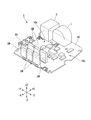
- FIG. 1 is a perspective view of a power conversion circuit board according to the first embodiment.
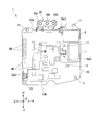
- FIG. 2 is a plan view of the power conversion circuit board according to the first embodiment.
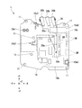
- FIG. 3 is a bottom view of the power conversion circuit board according to the first embodiment.
- FIG. 4 is a side view of the power conversion circuit board according to the first embodiment.
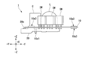
- FIG. 5 is a front view of the power conversion circuit board according to the first embodiment.
- the power conversion circuit board 1 according to the first embodiment is a circuit board constituting an inverter that converts DC power supplied from the outside through an input terminal (described later) into three-phase AC power.
- the power conversion circuit board 1 is integrally mounted on an electric compressor together with an AC motor that operates based on three-phase AC power output from the power conversion circuit board 1.
- the electric compressor is used, for example, in an air conditioner (car air conditioner) mounted on a vehicle.
- the electric compressor power conversion circuit board 1 receives an input of DC power from a battery or the like mounted on a vehicle.
- the power conversion circuit board 1 includes a board main body 10 and a bus bar support member 20.
- the substrate body 10 is a circuit board on which various circuit elements for forming a power conversion circuit (inverter) for converting direct current into alternating current are mounted. As shown in FIG. 1 etc., a part of the high voltage circuit 10a to which a high voltage is applied to the substrate surface (including both the + Z direction surface and the ⁇ Z direction surface) of the substrate body 10 The low voltage circuits 10b to which the low voltage is applied are separately arranged in different areas.
- the high voltage circuit 10a is a circuit of a large power system to which a high voltage necessary to drive an AC motor (not shown) is applied. Specifically, a direct current high voltage input from a battery or the like mounted on a vehicle is applied to the high voltage circuit 10a. The input DC high voltage is converted to three-phase AC power for driving the AC motor through the switching element SW. Each switching element SW switches to an ON state in which current flows and an OFF state in which the current is shut off based on a drive signal (gate input) from a low voltage circuit 10 b (described later). Two switching elements SW are provided corresponding to each of the U phase, the V phase, and the W phase forming three-phase alternating current.
- switching elements SW are mounted on the substrate surface of the substrate body 10. By repeating ON / OFF at the timing when each switching element SW is defined, AC power of three phases (U phase, V phase, W phase) is supplied to the AC motor.
- the switching element SW for example, an IGBT (Insulated Gate Bipolar Transistor) is representative, but in addition, a bipolar transistor, a MOSFET (Metal-Oxide-Semiconductor Field effect transistor) or the like may be used.
- the low voltage circuit 10b is a small signal circuit which operates at a lower voltage than the high voltage circuit 10a.
- a control chip such as a microcomputer and various sensors such as a current sensor are mounted on the low voltage circuit 10b, and the low voltage circuit 10b operates by applying a DC low voltage.
- the microcomputer mounted on the low voltage circuit 10b outputs desired drive signals according to the situation, for example, by outputting predetermined drive signals according to the detection results of various sensors to each switching element SW. To be controlled.
- the substrate body 10 according to the first embodiment is a multilayer wiring board in which a plurality of layers are stacked.
- the power supply pattern layer on which the power supply wiring to which the high voltage is applied is patterned and the GND (ground) on which the ground wiring to be grounded is patterned
- the pattern layer is laminated.
- FIGS. 1 to 5 the structure of the high voltage circuit 10a will be described in more detail with reference to FIGS.
- a high voltage input terminal 10a1, an RC circuit 10a2, a switching element SW, a bus bar supporting member 20, a capacitor C and an inductor L are electrically connected. It is connected to.
- the power conversion circuit board 1 will be mainly described with reference to FIG. 3 which is viewed from the bottom surface side ( ⁇ Z direction side).
- the + X direction side in FIG. 3 is described as the left side (left end side), the ⁇ X direction side as the right side (right end side), etc.
- the + Y direction side is the upper side (upper end side)
- the ⁇ Y direction side is the lower side. It is written as (lower end side) etc.
- the high voltage input terminal 10a1 is mounted on the substrate surface on the back surface side ( ⁇ Z direction side) of the substrate body 10 and on the left end side (+ X direction side) of the substrate body 10 (see FIG. 3) .
- a separately mounted battery is electrically connected to the high voltage input terminal 10a1, and a DC high voltage is applied from the battery.
- a capacitor C for high voltage and an inductor L are mounted on the surface of the substrate opposite to the surface on which the high voltage input terminal 10a1 is mounted (the + Z direction side) (see FIG. 2).
- the capacitor C for high voltage and the inductor L stabilize the DC high voltage from the battery.
- the DC high voltage input from the high voltage input terminal 10a1 passes through the RC circuit 10a2 disposed on the right end side (-X direction side) of the high voltage circuit 10a, and the six switching elements SW similarly mounted on the right end side Is input to
- the RC circuit 10a2 is a circuit in which a resistive element and a capacitor element are electrically connected, and functions as a low pass filter that removes high frequency components.
- the RC circuit 10a2 is a substrate surface of the substrate body 10, and at least a part of the RC circuit 10a2 is mounted in a space between the bus bar supporting member 20 described later and the substrate body 10 (see FIG. 3 etc.).
- the six switching elements SW are mounted on the lower side ( ⁇ Y direction side) of the RC circuit 10 a 2 in the substrate body 10.
- the bus bar support member 20 is adjacent to the substrate surface on the back surface side ( ⁇ Z direction side) of the substrate body 10 and to the left side (+ X direction side) of the area where the six switching elements SW are mounted. Will be placed.
- the bus bar support member 20 is disposed at a position spaced apart from the substrate surface on the back surface side of the substrate body 10 by a predetermined distance (see FIG. 4).
- three bus bars corresponding to each of the U phase, the V phase, and the W phase are mounted inside the bus bar support member 20 .
- the three bus bars mounted inside the bus bar support member 20 are the bus bar connection terminals 20 a located on the lower end side ( ⁇ Y direction side) of the bus bar support member 20 while maintaining a constant distance from the substrate surface of the substrate body 10.
- the three bus bars are arranged to cross over the high voltage circuit 10 a mounted from the left end side to the right end side of the substrate surface of the substrate body 10.
- the three bus bars mounted inside the bus bar support member 20 are electrically connected to the wires mounted on the surface of the substrate of the substrate body 10 at the bus bar connection terminals 20 a.
- the AC power of each phase generated by the ON / OFF driving of the switching element SW is input to the corresponding bus bars via the bus bar connection terminals 20a.
- the AC power corresponding to each of the U phase, V phase and W phase passes through the bus bar connecting terminal 20a located on the lower end side of the bus bar support member 20 and the bus bar extending from the upper end side to the high voltage output terminal 20b of each phase.
- the high voltage circuit 10a mounted on the power conversion circuit board 1 is a switching element from the high voltage input terminal 10a1 of the high voltage circuit 10a.
- the wiring to SW and the wiring from the switching element SW to the high voltage output terminal 20b are arranged to cross each other.
- the substrate main body portion 10 is a capacitor element provided for the purpose of reducing electromagnetic noise, and is a power supply wiring to which a high voltage is applied in the high voltage circuit 10a and a ground connected to the ground And a plurality of series capacitor groups 10a3 connected between the wires.
- the series capacitor group 10a3 is formed by connecting a plurality of (for example, five) capacitor elements (for example, several thousands pF order per element) in series (see FIGS. 2 and 3).
- Each capacitor element may be, for example, a general ceramic capacitor or the like.
- the series capacitor group 10a3 includes the front surface side (the surface on the + Z direction side) of the substrate body 10 and the back surface side (the ⁇ Z direction side) Are mounted at the same positions (positions overlapping each other as viewed from the + Z direction side or the ⁇ Z direction side) in the surface).
- the two series capacitor groups 10a3 mounted at the same position on the front surface side and the rear surface side are mounted such that the arrangement patterns of the plurality of capacitor elements are the same.
- casing of the electric compressor which is not shown in figure is provided in the board
- the power conversion circuit board 1 is screwed to the housing of the electric compressor through the fixing hole 11.
- a plurality of fixing holes 11 are provided one by one at each of the four corners of the substrate body 10, and a plurality of fixing holes 11 are provided near the center of the substrate body 10 (see FIGS. 2 and 3).
- a grounding land connected to a grounding wire is provided at the edge of the fixing hole 11.
- the fixing hole 11 is screwed, and the power conversion circuit board 1 is grounded through the grounding land provided at the edge of the fixing hole 11.
- the series capacitor group 10a3 described above is mounted in the vicinity of the fixing hole 11 corresponding to each of the fixing holes 11 (see FIGS. 2 and 3).
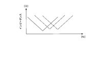
- FIG. 6A is a first diagram for explaining the characteristics of the series capacitor group according to the first embodiment.
- FIG. 6B is a second diagram illustrating the characteristics of the series capacitor group according to the first embodiment.
- the graph shown to FIG. 6A has shown the example of the frequency characteristic of the electromagnetic noise which arises from the circuit board 1 for power conversion (a vertical axis is noise intensity [dB], a horizontal axis is frequency [Hz]).
- the graph shown to FIG. 6B has shown the example of the frequency characteristic of the impedance of each capacitor element which comprises serial capacitor group 10a3 (A vertical axis
- the electromagnetic noise radiated from the power conversion circuit board 1 has a product-specific frequency characteristic due to the characteristics of the element to be mounted, the circuit pattern thereof, the applied voltage, the operating frequency and the like.
- the electromagnetic noise of the power conversion circuit board 1 exhibits an intensity higher than the predetermined value TH at a plurality of different frequencies f1 and f2.
- the five capacitor elements constituting the series capacitor group 10a3 respectively reduce the electromagnetic noise at the plurality of frequencies f1 and f2 corresponding to the plurality of frequencies f1 and f2 at which the electromagnetic noise is equal to or higher than the specified value TH. Selected to enable.
- the impedance ( ⁇ ) of the capacitor element has frequency characteristics as shown in FIG. 6B. That is, due to the resonance characteristic, there is a frequency band where the impedance is locally reduced.
- the frequency characteristics of the impedance of such a capacitor element differ depending on the type of the capacitor element to be selected and the like. Therefore, by combining the frequency characteristics of different impedances corresponding to the frequencies f1 and f2 where the electromagnetic noise is strong, the impedance of each capacitor element constituting the series capacitor group is set to a desired frequency (frequency f1, f2, etc.) Electromagnetic noise can be effectively reduced.
- FIG. 7 is a diagram for explaining the effects based on the structure of the high voltage circuit according to the first embodiment.
- the low voltage circuit 10b to which a low voltage is applied is the same as the high voltage circuit 10a to which a high voltage is applied.
- the substrate is divided into different areas and arranged one by one.
- the wiring from the high voltage input terminal 10a1 to the switching element SW in the high voltage circuit 10a (DC current Id is A bus bar is formed on the substrate surface of the substrate main body 10, and a wiring (a wiring through which an alternating current Ia flows) from the switching element SW to the high voltage output terminal 20b is provided at a predetermined distance from the substrate surface.
- electromagnetic noise (ringing noise etc.) generated by driving of the switching element SW is added to the RC circuit 10a2 and the wiring formed on the substrate surface of the substrate body 10 and a predetermined distance from the substrate surface It is absorbed also between the busbars provided to prevent the electromagnetic noise from being radiated to the outside.
- the wiring from the high voltage input terminal 10a1 to the switching element SW and the wiring from the switching element SW to the high voltage output terminal 20b cross each other. It is arranged as.
- the wiring through which the direct current Id flows in the high voltage circuit 10a (the wiring mounted on the substrate surface of the substrate body 10a) and the wiring through which the alternating current Id flows in the high voltage circuit 10a (supported by the bus bar support member 20) And the bus bar) to be three-dimensionally intersected.
- electromagnetic noise generated by driving of the switching element SW can be effectively absorbed at the intersections with each other, and the electromagnetic noise can be further suppressed from being radiated to the outside.
- the region occupied by the high voltage circuit 10 a in the power conversion circuit board 1 can be compactly integrated into one. Therefore, the entire power conversion circuit board 1 can be further miniaturized (space saving).
- the power conversion circuit board 1 it is provided between the wiring from the high voltage input terminal 10a1 to the switching element SW and the wiring from the switching element SW to the high voltage output terminal At least a part of the RC circuit 10a2 is provided in the space. In this way, the effect of removing electromagnetic noise can be obtained based on the function of the RC circuit 10a2 as a low pass filter. In order to secure a space necessary for mounting RC circuit 10a2, it is provided between the wiring from high voltage input terminal 10a1 to switching element SW and the wiring from switching element SW to the high voltage output terminal. Space can be used effectively. Therefore, further space saving of the power conversion circuit board 1 can be achieved.
- the high voltage circuit 10a includes the series capacitor group 10a3 including a plurality of capacitor elements connected in series between the power supply wiring and the ground wiring. It is characterized by By doing this, the voltage applied to each capacitor element is divided and reduced, so that the withstand voltage performance of the high voltage circuit 10a can be enhanced. In addition, even if one of the capacitor elements is broken and short circuited, it is possible to prevent the short circuit between the power supply wiring and the ground wiring by other capacitor elements connected in series. Furthermore, by doing this, it becomes possible to select each capacitor element constituting the series capacitor group 10a3 as desired, so the impedance characteristics of the series capacitor group 10a3 as a whole are matched to the electromagnetic noise unique to the product. Can be properly controlled. From the above, the influence of the electromagnetic noise on the external device can be reduced, and the breakdown voltage can be further increased.
- each capacitor element constituting the series capacitor group 10a3 corresponds to a plurality of frequencies at which the electromagnetic noise is equal to or higher than the specified value TH (FIG. 6A).
- different impedance characteristics frequency characteristics of impedance
- each of which can reduce electromagnetic noise at the plurality of frequencies.
- the electromagnetic noise of a desired frequency is effectively reduced by combining the frequency characteristics of different impedances in correspondence with the frequencies where the electromagnetic noise is strong (the frequencies f1 and f2 in FIG. 6A).
- the series capacitor group 10a3 is mounted in the same position in the surface side and back surface side of the board
- the power conversion circuit board 1 is disposed such that the wiring from the high voltage input terminal 10a1 to the switching element SW and the wiring from the switching element SW to the high voltage output terminal 20b intersect.
- the wiring from the high voltage input terminal 10a1 to the switching element SW and the wiring from the switching element SW to the high voltage output terminal 20b do not necessarily cross each other. Alternatively, for example, at least a part of the two may extend in an overlapping manner.
- the power conversion circuit board 1 is described as being connected to the RC circuit 10a2 for the purpose of reducing the electromagnetic noise according to the driving of the switching element SW, but in the other embodiments, It is not limited to this aspect. That is, the power conversion circuit board 1 according to another embodiment may not include the RC circuit 10a2. Further, in this case, the power conversion circuit board 1 according to the other embodiment may be configured such that only lands on which the RC circuit 10a2 can be mounted are formed. Thus, by providing only the region for mounting the RC circuit 10a2, it is possible to select the mounting / non-mounting of the RC circuit 10a2 according to the customer's request (degree of electromagnetic noise to be reduced). it can.
- the power conversion circuit board and the electric compressor described above can reduce the influence of electromagnetic noise while maintaining space saving performance.
Priority Applications (3)
| Application Number | Priority Date | Filing Date | Title |
|---|---|---|---|
| CN201680017085.1A CN107493688B (zh) | 2015-03-23 | 2016-02-15 | 电力变换用电路基板以及电动压缩机 |
| DE112016001382.5T DE112016001382T5 (de) | 2015-03-23 | 2016-02-15 | Energieumwandlungsleiterplatte und elektrischer kompressor |
| US15/559,607 US10218288B2 (en) | 2015-03-23 | 2016-02-15 | Power conversion circuit board, and electric compressor |
Applications Claiming Priority (2)
| Application Number | Priority Date | Filing Date | Title |
|---|---|---|---|
| JP2015-059208 | 2015-03-23 | ||
| JP2015059208A JP6399602B2 (ja) | 2015-03-23 | 2015-03-23 | 電力変換用回路基板及び電動圧縮機 |
Publications (1)
| Publication Number | Publication Date |
|---|---|
| WO2016152312A1 true WO2016152312A1 (ja) | 2016-09-29 |
Family
ID=56978359
Family Applications (1)
| Application Number | Title | Priority Date | Filing Date |
|---|---|---|---|
| PCT/JP2016/054251 WO2016152312A1 (ja) | 2015-03-23 | 2016-02-15 | 電力変換用回路基板及び電動圧縮機 |
Country Status (5)
| Country | Link |
|---|---|
| US (1) | US10218288B2 (zh) |
| JP (1) | JP6399602B2 (zh) |
| CN (1) | CN107493688B (zh) |
| DE (1) | DE112016001382T5 (zh) |
| WO (1) | WO2016152312A1 (zh) |
Cited By (1)
| Publication number | Priority date | Publication date | Assignee | Title |
|---|---|---|---|---|
| US20210135548A1 (en) * | 2018-01-12 | 2021-05-06 | Mahle International Gmbh | Control device for controlling an electric motor |
Families Citing this family (15)
| Publication number | Priority date | Publication date | Assignee | Title |
|---|---|---|---|---|
| NZ730234A (en) * | 2014-12-22 | 2019-03-29 | Mitsubishi Electric Corp | Printed wiring board, circuit board, and control unit |
| US9885196B2 (en) | 2015-01-26 | 2018-02-06 | Hayward Industries, Inc. | Pool cleaner power coupling |
| US9896858B1 (en) | 2017-05-11 | 2018-02-20 | Hayward Industries, Inc. | Hydrocyclonic pool cleaner |
| US10227081B2 (en) | 2017-05-11 | 2019-03-12 | Hayward Industries, Inc. | Pool cleaner caddy with retention mechanism |
| US10189490B2 (en) | 2017-05-11 | 2019-01-29 | Hayward Industries, Inc. | Pool cleaner caddy with removable wheel assemblies |
| US10161153B2 (en) | 2017-05-11 | 2018-12-25 | Hayward Industries, Inc. | Pool cleaner canister handle |
| US10676950B2 (en) | 2017-05-11 | 2020-06-09 | Hayward Industries, Inc. | Pool cleaner roller latch |
| US10214933B2 (en) * | 2017-05-11 | 2019-02-26 | Hayward Industries, Inc. | Pool cleaner power supply |
| US9885194B1 (en) | 2017-05-11 | 2018-02-06 | Hayward Industries, Inc. | Pool cleaner impeller subassembly |
| US10156083B2 (en) | 2017-05-11 | 2018-12-18 | Hayward Industries, Inc. | Pool cleaner power coupling |
| US10364905B2 (en) | 2017-05-11 | 2019-07-30 | Hayward Industries, Inc. | Pool cleaner check valve |
| CN109068475B (zh) * | 2018-09-07 | 2023-11-10 | 英迪迈智能驱动技术无锡股份有限公司 | 一种用于筒状电机的pcb布局结构 |
| KR20200044689A (ko) * | 2018-10-19 | 2020-04-29 | 한온시스템 주식회사 | 인버터 모듈 및 이를 포함하는 전동압축기 |
| DE102018222209B4 (de) | 2018-12-18 | 2023-03-30 | Vitesco Technologies Germany Gmbh | Schaltungsträger und leistungselektronische Schaltungsanordnung mit einem Schaltungsträger |
| JP7328792B2 (ja) * | 2019-05-17 | 2023-08-17 | 株式会社デンソー | 駆動装置 |
Citations (2)
| Publication number | Priority date | Publication date | Assignee | Title |
|---|---|---|---|---|
| JPH11189032A (ja) * | 1997-12-26 | 1999-07-13 | Matsushita Electric Ind Co Ltd | 空調用インバータシステム |
| JP2011229397A (ja) * | 2011-08-15 | 2011-11-10 | Mitsubishi Heavy Ind Ltd | 制御基板および制御装置 |
Family Cites Families (12)
| Publication number | Priority date | Publication date | Assignee | Title |
|---|---|---|---|---|
| CN1104181C (zh) | 1997-05-21 | 2003-03-26 | 国际商业机器公司 | 带集成双绞导线的印刷电路板 |
| JP2000151041A (ja) * | 1998-11-09 | 2000-05-30 | Yamaichi Electronics Co Ltd | プリント配線板 |
| JP4314513B2 (ja) * | 2003-06-18 | 2009-08-19 | アイシン・エィ・ダブリュ株式会社 | インバータノイズ除去装置 |
| EP1805880A2 (en) * | 2004-10-20 | 2007-07-11 | Ballard Power Systems Corporation | Power system method and apparatus |
| JP5039356B2 (ja) * | 2006-10-13 | 2012-10-03 | 三菱重工業株式会社 | 制御基板および電動圧縮機の制御装置ならびに電動圧縮機 |
| WO2008050706A1 (fr) | 2006-10-24 | 2008-05-02 | Panasonic Corporation | Tableau de connexions imprimé, procédé de fabrication d'un tableau de connexions imprimé et dispositif électrique |
| JP4981483B2 (ja) | 2007-03-01 | 2012-07-18 | 三菱重工業株式会社 | 一体型電動圧縮機 |
| JP5091521B2 (ja) * | 2007-03-29 | 2012-12-05 | 三菱重工業株式会社 | 一体型電動圧縮機 |
| JP4988665B2 (ja) * | 2008-08-06 | 2012-08-01 | 日立オートモティブシステムズ株式会社 | 半導体装置および半導体装置を用いた電力変換装置 |
| JP5422468B2 (ja) * | 2010-04-01 | 2014-02-19 | 日立オートモティブシステムズ株式会社 | 電力変換装置 |
| JP5417314B2 (ja) | 2010-12-27 | 2014-02-12 | 日立オートモティブシステムズ株式会社 | 電力変換装置 |
| JP5508357B2 (ja) * | 2011-07-29 | 2014-05-28 | 日立オートモティブシステムズ株式会社 | 電力変換装置 |
-
2015
- 2015-03-23 JP JP2015059208A patent/JP6399602B2/ja active Active
-
2016
- 2016-02-15 CN CN201680017085.1A patent/CN107493688B/zh active Active
- 2016-02-15 US US15/559,607 patent/US10218288B2/en active Active
- 2016-02-15 WO PCT/JP2016/054251 patent/WO2016152312A1/ja active Application Filing
- 2016-02-15 DE DE112016001382.5T patent/DE112016001382T5/de active Pending
Patent Citations (2)
| Publication number | Priority date | Publication date | Assignee | Title |
|---|---|---|---|---|
| JPH11189032A (ja) * | 1997-12-26 | 1999-07-13 | Matsushita Electric Ind Co Ltd | 空調用インバータシステム |
| JP2011229397A (ja) * | 2011-08-15 | 2011-11-10 | Mitsubishi Heavy Ind Ltd | 制御基板および制御装置 |
Cited By (2)
| Publication number | Priority date | Publication date | Assignee | Title |
|---|---|---|---|---|
| US20210135548A1 (en) * | 2018-01-12 | 2021-05-06 | Mahle International Gmbh | Control device for controlling an electric motor |
| US11682948B2 (en) * | 2018-01-12 | 2023-06-20 | Mahle International Gmbh | Control device for controlling an electric motor comprising a plate penetrated by an electronic power component |
Also Published As
| Publication number | Publication date |
|---|---|
| US20180069487A1 (en) | 2018-03-08 |
| JP6399602B2 (ja) | 2018-10-03 |
| DE112016001382T5 (de) | 2017-12-14 |
| CN107493688B (zh) | 2020-01-17 |
| US10218288B2 (en) | 2019-02-26 |
| CN107493688A (zh) | 2017-12-19 |
| JP2016178846A (ja) | 2016-10-06 |
Similar Documents
| Publication | Publication Date | Title |
|---|---|---|
| WO2016152312A1 (ja) | 電力変換用回路基板及び電動圧縮機 | |
| WO2016152313A1 (ja) | 電力変換用回路基板及び電動圧縮機 | |
| US11418111B2 (en) | Power conversion circuit board and electric compressor | |
| JP5039356B2 (ja) | 制御基板および電動圧縮機の制御装置ならびに電動圧縮機 | |
| EP3654504B1 (en) | Voltage filter and power conversion device | |
| CN108370196B (zh) | 抗干扰装置、电子组件和抗干扰装置的用途 | |
| WO2015056321A1 (ja) | ノイズフィルタ | |
| CN116530005A (zh) | 功率转换装置 | |
| CN102782843B (zh) | 半导体装置 | |
| JP5186029B2 (ja) | 制御基板及び電動圧縮機の制御装置 | |
| US9866102B2 (en) | Power conversion device | |
| JP2020014374A (ja) | 電力変換用回路基板及び電動圧縮機 | |
| US11910523B2 (en) | Bus bar | |
| US11524349B2 (en) | Substrate | |
| JP2006310435A (ja) | 多層プリント基板 | |
| US20240106320A1 (en) | Power conversion device | |
| JP6975564B2 (ja) | 電力変換装置 | |
| US10658925B2 (en) | Circuit board to transform an entry phase in at least one output phase and direct-current-motor with such circuit board | |
| JP2013149755A (ja) | スイッチング素子装置 | |
| JP2014082845A (ja) | 回路装置 |
Legal Events
| Date | Code | Title | Description |
|---|---|---|---|
| 121 | Ep: the epo has been informed by wipo that ep was designated in this application |
Ref document number: 16768215 Country of ref document: EP Kind code of ref document: A1 |
|
| WWE | Wipo information: entry into national phase |
Ref document number: 15559607 Country of ref document: US |
|
| WWE | Wipo information: entry into national phase |
Ref document number: 112016001382 Country of ref document: DE |
|
| 122 | Ep: pct application non-entry in european phase |
Ref document number: 16768215 Country of ref document: EP Kind code of ref document: A1 |