WO2016152312A1 - Power conversion circuit board, and electric compressor - Google Patents
Power conversion circuit board, and electric compressor Download PDFInfo
- Publication number
- WO2016152312A1 WO2016152312A1 PCT/JP2016/054251 JP2016054251W WO2016152312A1 WO 2016152312 A1 WO2016152312 A1 WO 2016152312A1 JP 2016054251 W JP2016054251 W JP 2016054251W WO 2016152312 A1 WO2016152312 A1 WO 2016152312A1
- Authority
- WO
- WIPO (PCT)
- Prior art keywords
- high voltage
- power conversion
- circuit board
- circuit
- switching element
- Prior art date
Links
Images


Classifications
-
- H—ELECTRICITY
- H02—GENERATION; CONVERSION OR DISTRIBUTION OF ELECTRIC POWER
- H02M—APPARATUS FOR CONVERSION BETWEEN AC AND AC, BETWEEN AC AND DC, OR BETWEEN DC AND DC, AND FOR USE WITH MAINS OR SIMILAR POWER SUPPLY SYSTEMS; CONVERSION OF DC OR AC INPUT POWER INTO SURGE OUTPUT POWER; CONTROL OR REGULATION THEREOF
- H02M7/00—Conversion of ac power input into dc power output; Conversion of dc power input into ac power output
- H02M7/42—Conversion of dc power input into ac power output without possibility of reversal
- H02M7/44—Conversion of dc power input into ac power output without possibility of reversal by static converters
- H02M7/48—Conversion of dc power input into ac power output without possibility of reversal by static converters using discharge tubes with control electrode or semiconductor devices with control electrode
-
- F—MECHANICAL ENGINEERING; LIGHTING; HEATING; WEAPONS; BLASTING
- F04—POSITIVE - DISPLACEMENT MACHINES FOR LIQUIDS; PUMPS FOR LIQUIDS OR ELASTIC FLUIDS
- F04B—POSITIVE-DISPLACEMENT MACHINES FOR LIQUIDS; PUMPS
- F04B35/00—Piston pumps specially adapted for elastic fluids and characterised by the driving means to their working members, or by combination with, or adaptation to, specific driving engines or motors, not otherwise provided for
- F04B35/04—Piston pumps specially adapted for elastic fluids and characterised by the driving means to their working members, or by combination with, or adaptation to, specific driving engines or motors, not otherwise provided for the means being electric
-
- F—MECHANICAL ENGINEERING; LIGHTING; HEATING; WEAPONS; BLASTING
- F04—POSITIVE - DISPLACEMENT MACHINES FOR LIQUIDS; PUMPS FOR LIQUIDS OR ELASTIC FLUIDS
- F04B—POSITIVE-DISPLACEMENT MACHINES FOR LIQUIDS; PUMPS
- F04B39/00—Component parts, details, or accessories, of pumps or pumping systems specially adapted for elastic fluids, not otherwise provided for in, or of interest apart from, groups F04B25/00 - F04B37/00
- F04B39/12—Casings; Cylinders; Cylinder heads; Fluid connections
- F04B39/121—Casings
-
- H—ELECTRICITY
- H02—GENERATION; CONVERSION OR DISTRIBUTION OF ELECTRIC POWER
- H02K—DYNAMO-ELECTRIC MACHINES
- H02K11/00—Structural association of dynamo-electric machines with electric components or with devices for shielding, monitoring or protection
- H02K11/30—Structural association with control circuits or drive circuits
- H02K11/33—Drive circuits, e.g. power electronics
-
- H—ELECTRICITY
- H02—GENERATION; CONVERSION OR DISTRIBUTION OF ELECTRIC POWER
- H02P—CONTROL OR REGULATION OF ELECTRIC MOTORS, ELECTRIC GENERATORS OR DYNAMO-ELECTRIC CONVERTERS; CONTROLLING TRANSFORMERS, REACTORS OR CHOKE COILS
- H02P27/00—Arrangements or methods for the control of AC motors characterised by the kind of supply voltage
- H02P27/04—Arrangements or methods for the control of AC motors characterised by the kind of supply voltage using variable-frequency supply voltage, e.g. inverter or converter supply voltage
- H02P27/06—Arrangements or methods for the control of AC motors characterised by the kind of supply voltage using variable-frequency supply voltage, e.g. inverter or converter supply voltage using dc to ac converters or inverters
-
- H—ELECTRICITY
- H05—ELECTRIC TECHNIQUES NOT OTHERWISE PROVIDED FOR
- H05K—PRINTED CIRCUITS; CASINGS OR CONSTRUCTIONAL DETAILS OF ELECTRIC APPARATUS; MANUFACTURE OF ASSEMBLAGES OF ELECTRICAL COMPONENTS
- H05K1/00—Printed circuits
- H05K1/02—Details
-
- H—ELECTRICITY
- H05—ELECTRIC TECHNIQUES NOT OTHERWISE PROVIDED FOR
- H05K—PRINTED CIRCUITS; CASINGS OR CONSTRUCTIONAL DETAILS OF ELECTRIC APPARATUS; MANUFACTURE OF ASSEMBLAGES OF ELECTRICAL COMPONENTS
- H05K1/00—Printed circuits
- H05K1/02—Details
- H05K1/0213—Electrical arrangements not otherwise provided for
- H05K1/0263—High current adaptations, e.g. printed high current conductors or using auxiliary non-printed means; Fine and coarse circuit patterns on one circuit board
-
- F—MECHANICAL ENGINEERING; LIGHTING; HEATING; WEAPONS; BLASTING
- F04—POSITIVE - DISPLACEMENT MACHINES FOR LIQUIDS; PUMPS FOR LIQUIDS OR ELASTIC FLUIDS
- F04B—POSITIVE-DISPLACEMENT MACHINES FOR LIQUIDS; PUMPS
- F04B2203/00—Motor parameters
- F04B2203/02—Motor parameters of rotating electric motors
- F04B2203/0204—Frequency of the electric current
-
- H—ELECTRICITY
- H02—GENERATION; CONVERSION OR DISTRIBUTION OF ELECTRIC POWER
- H02M—APPARATUS FOR CONVERSION BETWEEN AC AND AC, BETWEEN AC AND DC, OR BETWEEN DC AND DC, AND FOR USE WITH MAINS OR SIMILAR POWER SUPPLY SYSTEMS; CONVERSION OF DC OR AC INPUT POWER INTO SURGE OUTPUT POWER; CONTROL OR REGULATION THEREOF
- H02M7/00—Conversion of ac power input into dc power output; Conversion of dc power input into ac power output
- H02M7/003—Constructional details, e.g. physical layout, assembly, wiring or busbar connections
-
- H—ELECTRICITY
- H05—ELECTRIC TECHNIQUES NOT OTHERWISE PROVIDED FOR
- H05K—PRINTED CIRCUITS; CASINGS OR CONSTRUCTIONAL DETAILS OF ELECTRIC APPARATUS; MANUFACTURE OF ASSEMBLAGES OF ELECTRICAL COMPONENTS
- H05K1/00—Printed circuits
- H05K1/02—Details
- H05K1/0213—Electrical arrangements not otherwise provided for
- H05K1/0254—High voltage adaptations; Electrical insulation details; Overvoltage or electrostatic discharge protection ; Arrangements for regulating voltages or for using plural voltages
- H05K1/0262—Arrangements for regulating voltages or for using plural voltages
-
- H—ELECTRICITY
- H05—ELECTRIC TECHNIQUES NOT OTHERWISE PROVIDED FOR
- H05K—PRINTED CIRCUITS; CASINGS OR CONSTRUCTIONAL DETAILS OF ELECTRIC APPARATUS; MANUFACTURE OF ASSEMBLAGES OF ELECTRICAL COMPONENTS
- H05K2201/00—Indexing scheme relating to printed circuits covered by H05K1/00
- H05K2201/10—Details of components or other objects attached to or integrated in a printed circuit board
- H05K2201/10007—Types of components
- H05K2201/10166—Transistor
-
- H—ELECTRICITY
- H05—ELECTRIC TECHNIQUES NOT OTHERWISE PROVIDED FOR
- H05K—PRINTED CIRCUITS; CASINGS OR CONSTRUCTIONAL DETAILS OF ELECTRIC APPARATUS; MANUFACTURE OF ASSEMBLAGES OF ELECTRICAL COMPONENTS
- H05K2201/00—Indexing scheme relating to printed circuits covered by H05K1/00
- H05K2201/10—Details of components or other objects attached to or integrated in a printed circuit board
- H05K2201/10007—Types of components
- H05K2201/10189—Non-printed connector
-
- H—ELECTRICITY
- H05—ELECTRIC TECHNIQUES NOT OTHERWISE PROVIDED FOR
- H05K—PRINTED CIRCUITS; CASINGS OR CONSTRUCTIONAL DETAILS OF ELECTRIC APPARATUS; MANUFACTURE OF ASSEMBLAGES OF ELECTRICAL COMPONENTS
- H05K2201/00—Indexing scheme relating to printed circuits covered by H05K1/00
- H05K2201/10—Details of components or other objects attached to or integrated in a printed circuit board
- H05K2201/10227—Other objects, e.g. metallic pieces
- H05K2201/10272—Busbars, i.e. thick metal bars mounted on the PCB as high-current conductors
Definitions
- the present invention relates to a circuit board for power conversion and a motor-driven compressor.
- Priority is claimed on Japanese Patent Application No. 2015-059208, filed March 23, 2015, the content of which is incorporated herein by reference.
- a compressor constituting an on-vehicle air conditioner, a motor for driving the compressor, and a circuit board for controlling the compressor are integrally configured.
- An integrated electric compressor is provided (see, for example, Patent Document 1).
- the objective is to provide the circuit board for electric power conversion which can reduce the influence of electromagnetic noise, and a motor-driven compressor, maintaining space saving property. It is in.
- One embodiment of the present invention is a substrate mounted with a power conversion circuit that converts direct current into alternating current, and the low voltage circuit to which a low voltage is applied is the same as the high voltage circuit to which a high voltage is applied.
- the power conversion circuit board is separately disposed in different areas of the substrate surface.
- a wire from a high voltage input terminal to a switching element in the high voltage circuit is formed on the surface of the substrate, and Wiring to the voltage output terminal is constituted by a bus bar provided at a predetermined distance from the substrate surface.
- a wiring from the high voltage input terminal to the switching element and a wiring from the switching element to the high voltage output terminal cross each other. It is arranged.
- electromagnetic noise generated by driving the switching elements can be effectively absorbed at the intersections with each other, and the electromagnetic noise can be further suppressed from being radiated to the outside.
- the region occupied by the high voltage circuit in the power conversion circuit board can be compactly integrated into one. Therefore, the entire power conversion circuit board can be further saved in space.
- the power conversion circuit board described above is provided between the wiring from the high voltage input terminal to the switching element and the wiring from the switching element to the high voltage output terminal. At least a part of the RC circuit is provided in the space. With such a configuration, it is possible to obtain an electromagnetic noise removal effect by the RC circuit. Also, in order to secure the space necessary for mounting the RC circuit, the space provided between the wiring from the high voltage input terminal to the switching element and the wiring from the switching element to the high voltage output terminal It can be used effectively. Therefore, further space saving of the circuit board for power conversion can be achieved.
- Another embodiment of the present invention is a motor-driven compressor including the above-described power conversion circuit board and a motor that operates based on AC power supplied from the power conversion circuit board.
- the power conversion circuit board and the electric compressor described above can reduce the influence of electromagnetic noise while maintaining space saving performance.
- FIG. 1 explaining the characteristic of the series capacitor group which concerns on 1st Embodiment.
- FIG. 2 explaining the characteristic of the series capacitor group which concerns on 1st Embodiment. It is a figure explaining the effect based on the structure of the high voltage circuit which concerns on 1st Embodiment.
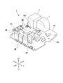
- FIG. 1 is a perspective view of a power conversion circuit board according to the first embodiment.
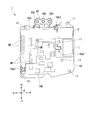
- FIG. 2 is a plan view of the power conversion circuit board according to the first embodiment.
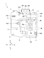
- FIG. 3 is a bottom view of the power conversion circuit board according to the first embodiment.
- FIG. 4 is a side view of the power conversion circuit board according to the first embodiment.
- FIG. 5 is a front view of the power conversion circuit board according to the first embodiment.
- the power conversion circuit board 1 according to the first embodiment is a circuit board constituting an inverter that converts DC power supplied from the outside through an input terminal (described later) into three-phase AC power.
- the power conversion circuit board 1 is integrally mounted on an electric compressor together with an AC motor that operates based on three-phase AC power output from the power conversion circuit board 1.
- the electric compressor is used, for example, in an air conditioner (car air conditioner) mounted on a vehicle.
- the electric compressor power conversion circuit board 1 receives an input of DC power from a battery or the like mounted on a vehicle.
- the power conversion circuit board 1 includes a board main body 10 and a bus bar support member 20.
- the substrate body 10 is a circuit board on which various circuit elements for forming a power conversion circuit (inverter) for converting direct current into alternating current are mounted. As shown in FIG. 1 etc., a part of the high voltage circuit 10a to which a high voltage is applied to the substrate surface (including both the + Z direction surface and the ⁇ Z direction surface) of the substrate body 10 The low voltage circuits 10b to which the low voltage is applied are separately arranged in different areas.
- the high voltage circuit 10a is a circuit of a large power system to which a high voltage necessary to drive an AC motor (not shown) is applied. Specifically, a direct current high voltage input from a battery or the like mounted on a vehicle is applied to the high voltage circuit 10a. The input DC high voltage is converted to three-phase AC power for driving the AC motor through the switching element SW. Each switching element SW switches to an ON state in which current flows and an OFF state in which the current is shut off based on a drive signal (gate input) from a low voltage circuit 10 b (described later). Two switching elements SW are provided corresponding to each of the U phase, the V phase, and the W phase forming three-phase alternating current.
- switching elements SW are mounted on the substrate surface of the substrate body 10. By repeating ON / OFF at the timing when each switching element SW is defined, AC power of three phases (U phase, V phase, W phase) is supplied to the AC motor.
- the switching element SW for example, an IGBT (Insulated Gate Bipolar Transistor) is representative, but in addition, a bipolar transistor, a MOSFET (Metal-Oxide-Semiconductor Field effect transistor) or the like may be used.
- the low voltage circuit 10b is a small signal circuit which operates at a lower voltage than the high voltage circuit 10a.
- a control chip such as a microcomputer and various sensors such as a current sensor are mounted on the low voltage circuit 10b, and the low voltage circuit 10b operates by applying a DC low voltage.
- the microcomputer mounted on the low voltage circuit 10b outputs desired drive signals according to the situation, for example, by outputting predetermined drive signals according to the detection results of various sensors to each switching element SW. To be controlled.
- the substrate body 10 according to the first embodiment is a multilayer wiring board in which a plurality of layers are stacked.
- the power supply pattern layer on which the power supply wiring to which the high voltage is applied is patterned and the GND (ground) on which the ground wiring to be grounded is patterned
- the pattern layer is laminated.
- FIGS. 1 to 5 the structure of the high voltage circuit 10a will be described in more detail with reference to FIGS.
- a high voltage input terminal 10a1, an RC circuit 10a2, a switching element SW, a bus bar supporting member 20, a capacitor C and an inductor L are electrically connected. It is connected to.
- the power conversion circuit board 1 will be mainly described with reference to FIG. 3 which is viewed from the bottom surface side ( ⁇ Z direction side).
- the + X direction side in FIG. 3 is described as the left side (left end side), the ⁇ X direction side as the right side (right end side), etc.
- the + Y direction side is the upper side (upper end side)
- the ⁇ Y direction side is the lower side. It is written as (lower end side) etc.
- the high voltage input terminal 10a1 is mounted on the substrate surface on the back surface side ( ⁇ Z direction side) of the substrate body 10 and on the left end side (+ X direction side) of the substrate body 10 (see FIG. 3) .
- a separately mounted battery is electrically connected to the high voltage input terminal 10a1, and a DC high voltage is applied from the battery.
- a capacitor C for high voltage and an inductor L are mounted on the surface of the substrate opposite to the surface on which the high voltage input terminal 10a1 is mounted (the + Z direction side) (see FIG. 2).
- the capacitor C for high voltage and the inductor L stabilize the DC high voltage from the battery.
- the DC high voltage input from the high voltage input terminal 10a1 passes through the RC circuit 10a2 disposed on the right end side (-X direction side) of the high voltage circuit 10a, and the six switching elements SW similarly mounted on the right end side Is input to
- the RC circuit 10a2 is a circuit in which a resistive element and a capacitor element are electrically connected, and functions as a low pass filter that removes high frequency components.
- the RC circuit 10a2 is a substrate surface of the substrate body 10, and at least a part of the RC circuit 10a2 is mounted in a space between the bus bar supporting member 20 described later and the substrate body 10 (see FIG. 3 etc.).
- the six switching elements SW are mounted on the lower side ( ⁇ Y direction side) of the RC circuit 10 a 2 in the substrate body 10.
- the bus bar support member 20 is adjacent to the substrate surface on the back surface side ( ⁇ Z direction side) of the substrate body 10 and to the left side (+ X direction side) of the area where the six switching elements SW are mounted. Will be placed.
- the bus bar support member 20 is disposed at a position spaced apart from the substrate surface on the back surface side of the substrate body 10 by a predetermined distance (see FIG. 4).
- three bus bars corresponding to each of the U phase, the V phase, and the W phase are mounted inside the bus bar support member 20 .
- the three bus bars mounted inside the bus bar support member 20 are the bus bar connection terminals 20 a located on the lower end side ( ⁇ Y direction side) of the bus bar support member 20 while maintaining a constant distance from the substrate surface of the substrate body 10.
- the three bus bars are arranged to cross over the high voltage circuit 10 a mounted from the left end side to the right end side of the substrate surface of the substrate body 10.
- the three bus bars mounted inside the bus bar support member 20 are electrically connected to the wires mounted on the surface of the substrate of the substrate body 10 at the bus bar connection terminals 20 a.
- the AC power of each phase generated by the ON / OFF driving of the switching element SW is input to the corresponding bus bars via the bus bar connection terminals 20a.
- the AC power corresponding to each of the U phase, V phase and W phase passes through the bus bar connecting terminal 20a located on the lower end side of the bus bar support member 20 and the bus bar extending from the upper end side to the high voltage output terminal 20b of each phase.
- the high voltage circuit 10a mounted on the power conversion circuit board 1 is a switching element from the high voltage input terminal 10a1 of the high voltage circuit 10a.
- the wiring to SW and the wiring from the switching element SW to the high voltage output terminal 20b are arranged to cross each other.
- the substrate main body portion 10 is a capacitor element provided for the purpose of reducing electromagnetic noise, and is a power supply wiring to which a high voltage is applied in the high voltage circuit 10a and a ground connected to the ground And a plurality of series capacitor groups 10a3 connected between the wires.
- the series capacitor group 10a3 is formed by connecting a plurality of (for example, five) capacitor elements (for example, several thousands pF order per element) in series (see FIGS. 2 and 3).
- Each capacitor element may be, for example, a general ceramic capacitor or the like.
- the series capacitor group 10a3 includes the front surface side (the surface on the + Z direction side) of the substrate body 10 and the back surface side (the ⁇ Z direction side) Are mounted at the same positions (positions overlapping each other as viewed from the + Z direction side or the ⁇ Z direction side) in the surface).
- the two series capacitor groups 10a3 mounted at the same position on the front surface side and the rear surface side are mounted such that the arrangement patterns of the plurality of capacitor elements are the same.
- casing of the electric compressor which is not shown in figure is provided in the board
- the power conversion circuit board 1 is screwed to the housing of the electric compressor through the fixing hole 11.
- a plurality of fixing holes 11 are provided one by one at each of the four corners of the substrate body 10, and a plurality of fixing holes 11 are provided near the center of the substrate body 10 (see FIGS. 2 and 3).
- a grounding land connected to a grounding wire is provided at the edge of the fixing hole 11.
- the fixing hole 11 is screwed, and the power conversion circuit board 1 is grounded through the grounding land provided at the edge of the fixing hole 11.
- the series capacitor group 10a3 described above is mounted in the vicinity of the fixing hole 11 corresponding to each of the fixing holes 11 (see FIGS. 2 and 3).
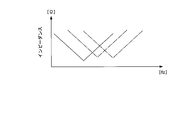
- FIG. 6A is a first diagram for explaining the characteristics of the series capacitor group according to the first embodiment.
- FIG. 6B is a second diagram illustrating the characteristics of the series capacitor group according to the first embodiment.
- the graph shown to FIG. 6A has shown the example of the frequency characteristic of the electromagnetic noise which arises from the circuit board 1 for power conversion (a vertical axis is noise intensity [dB], a horizontal axis is frequency [Hz]).
- the graph shown to FIG. 6B has shown the example of the frequency characteristic of the impedance of each capacitor element which comprises serial capacitor group 10a3 (A vertical axis
- the electromagnetic noise radiated from the power conversion circuit board 1 has a product-specific frequency characteristic due to the characteristics of the element to be mounted, the circuit pattern thereof, the applied voltage, the operating frequency and the like.
- the electromagnetic noise of the power conversion circuit board 1 exhibits an intensity higher than the predetermined value TH at a plurality of different frequencies f1 and f2.
- the five capacitor elements constituting the series capacitor group 10a3 respectively reduce the electromagnetic noise at the plurality of frequencies f1 and f2 corresponding to the plurality of frequencies f1 and f2 at which the electromagnetic noise is equal to or higher than the specified value TH. Selected to enable.
- the impedance ( ⁇ ) of the capacitor element has frequency characteristics as shown in FIG. 6B. That is, due to the resonance characteristic, there is a frequency band where the impedance is locally reduced.
- the frequency characteristics of the impedance of such a capacitor element differ depending on the type of the capacitor element to be selected and the like. Therefore, by combining the frequency characteristics of different impedances corresponding to the frequencies f1 and f2 where the electromagnetic noise is strong, the impedance of each capacitor element constituting the series capacitor group is set to a desired frequency (frequency f1, f2, etc.) Electromagnetic noise can be effectively reduced.
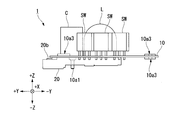
- FIG. 7 is a diagram for explaining the effects based on the structure of the high voltage circuit according to the first embodiment.
- the low voltage circuit 10b to which a low voltage is applied is the same as the high voltage circuit 10a to which a high voltage is applied.
- the substrate is divided into different areas and arranged one by one.
- the wiring from the high voltage input terminal 10a1 to the switching element SW in the high voltage circuit 10a (DC current Id is A bus bar is formed on the substrate surface of the substrate main body 10, and a wiring (a wiring through which an alternating current Ia flows) from the switching element SW to the high voltage output terminal 20b is provided at a predetermined distance from the substrate surface.
- electromagnetic noise (ringing noise etc.) generated by driving of the switching element SW is added to the RC circuit 10a2 and the wiring formed on the substrate surface of the substrate body 10 and a predetermined distance from the substrate surface It is absorbed also between the busbars provided to prevent the electromagnetic noise from being radiated to the outside.
- the wiring from the high voltage input terminal 10a1 to the switching element SW and the wiring from the switching element SW to the high voltage output terminal 20b cross each other. It is arranged as.
- the wiring through which the direct current Id flows in the high voltage circuit 10a (the wiring mounted on the substrate surface of the substrate body 10a) and the wiring through which the alternating current Id flows in the high voltage circuit 10a (supported by the bus bar support member 20) And the bus bar) to be three-dimensionally intersected.
- electromagnetic noise generated by driving of the switching element SW can be effectively absorbed at the intersections with each other, and the electromagnetic noise can be further suppressed from being radiated to the outside.
- the region occupied by the high voltage circuit 10 a in the power conversion circuit board 1 can be compactly integrated into one. Therefore, the entire power conversion circuit board 1 can be further miniaturized (space saving).
- the power conversion circuit board 1 it is provided between the wiring from the high voltage input terminal 10a1 to the switching element SW and the wiring from the switching element SW to the high voltage output terminal At least a part of the RC circuit 10a2 is provided in the space. In this way, the effect of removing electromagnetic noise can be obtained based on the function of the RC circuit 10a2 as a low pass filter. In order to secure a space necessary for mounting RC circuit 10a2, it is provided between the wiring from high voltage input terminal 10a1 to switching element SW and the wiring from switching element SW to the high voltage output terminal. Space can be used effectively. Therefore, further space saving of the power conversion circuit board 1 can be achieved.
- the high voltage circuit 10a includes the series capacitor group 10a3 including a plurality of capacitor elements connected in series between the power supply wiring and the ground wiring. It is characterized by By doing this, the voltage applied to each capacitor element is divided and reduced, so that the withstand voltage performance of the high voltage circuit 10a can be enhanced. In addition, even if one of the capacitor elements is broken and short circuited, it is possible to prevent the short circuit between the power supply wiring and the ground wiring by other capacitor elements connected in series. Furthermore, by doing this, it becomes possible to select each capacitor element constituting the series capacitor group 10a3 as desired, so the impedance characteristics of the series capacitor group 10a3 as a whole are matched to the electromagnetic noise unique to the product. Can be properly controlled. From the above, the influence of the electromagnetic noise on the external device can be reduced, and the breakdown voltage can be further increased.
- each capacitor element constituting the series capacitor group 10a3 corresponds to a plurality of frequencies at which the electromagnetic noise is equal to or higher than the specified value TH (FIG. 6A).
- different impedance characteristics frequency characteristics of impedance
- each of which can reduce electromagnetic noise at the plurality of frequencies.
- the electromagnetic noise of a desired frequency is effectively reduced by combining the frequency characteristics of different impedances in correspondence with the frequencies where the electromagnetic noise is strong (the frequencies f1 and f2 in FIG. 6A).
- the series capacitor group 10a3 is mounted in the same position in the surface side and back surface side of the board
- the power conversion circuit board 1 is disposed such that the wiring from the high voltage input terminal 10a1 to the switching element SW and the wiring from the switching element SW to the high voltage output terminal 20b intersect.
- the wiring from the high voltage input terminal 10a1 to the switching element SW and the wiring from the switching element SW to the high voltage output terminal 20b do not necessarily cross each other. Alternatively, for example, at least a part of the two may extend in an overlapping manner.
- the power conversion circuit board 1 is described as being connected to the RC circuit 10a2 for the purpose of reducing the electromagnetic noise according to the driving of the switching element SW, but in the other embodiments, It is not limited to this aspect. That is, the power conversion circuit board 1 according to another embodiment may not include the RC circuit 10a2. Further, in this case, the power conversion circuit board 1 according to the other embodiment may be configured such that only lands on which the RC circuit 10a2 can be mounted are formed. Thus, by providing only the region for mounting the RC circuit 10a2, it is possible to select the mounting / non-mounting of the RC circuit 10a2 according to the customer's request (degree of electromagnetic noise to be reduced). it can.
- the power conversion circuit board and the electric compressor described above can reduce the influence of electromagnetic noise while maintaining space saving performance.
Abstract
This power conversion circuit board (1) has a power conversion circuit mounted thereon for converting direct current to alternating current, and comprises a low voltage circuit (10b), to which a low voltage is applied, and a high-voltage circuit (10a), to which a high voltage is applied, disposed on different areas on the same board surface. Further, the high-voltage circuit (10a) is configured from a busbar, with part of the wiring thereof formed on the board surface, and the other part of said wiring separated by a prescribed distance from the board surface.
Description
本発明は、電力変換用回路基板及び電動圧縮機に関する。
本願は、2015年3月23日に、日本に出願された特願2015-059208号に基づき優先権を主張し、その内容をここに援用する。 The present invention relates to a circuit board for power conversion and a motor-driven compressor.
Priority is claimed on Japanese Patent Application No. 2015-059208, filed March 23, 2015, the content of which is incorporated herein by reference.
車載用空気調和機は、例えば、車両内の限られた空間に各種構成機器を収容する必要性から、高い省スペース性が要求されている。このため、近年、省スペース性を高める目的で、車載用空気調和機を構成する圧縮機と、圧縮機を駆動するためのモータと、圧縮機を制御するための回路基板と、が一体に構成された一体型電動圧縮機が提供されている(例えば、特許文献1参照)。
In the on-vehicle air conditioner, for example, since it is necessary to accommodate various components in a limited space in a vehicle, high space saving is required. For this reason, in recent years, for the purpose of improving space saving property, a compressor constituting an on-vehicle air conditioner, a motor for driving the compressor, and a circuit board for controlling the compressor are integrally configured. An integrated electric compressor is provided (see, for example, Patent Document 1).
しかしながら、一体化された電動圧縮機が有する回路基板においては、比較的低電圧で動作する小信号系の回路と、モータを駆動させるために必要な高電圧が印加される大電力系の回路と、が共存する。省スペース化のため、上記小信号系の回路を構成する素子と大電力系の回路を構成する素子との密度が高まると、大電力系の回路における動作に基づいて放射される種々の電磁ノイズが小信号系の回路における動作に悪影響を及ぼすことが想定される。
However, in the circuit board of the integrated motor compressor, a small signal system circuit operating at a relatively low voltage, and a high power system circuit to which a high voltage necessary to drive the motor is applied. , Co-exist. When the density of the elements forming the small signal system circuit and the elements forming the high power system circuit increases for space saving, various electromagnetic noises radiated based on the operation in the high power system circuit Is expected to adversely affect the operation in the small signal circuit.
本発明は、上記課題に鑑みてなされたものであって、その目的は、省スペース性を維持しながらも、電磁ノイズの影響を低減可能な電力変換用回路基板及び電動圧縮機を提供することにある。
This invention is made in view of the said subject, Comprising: The objective is to provide the circuit board for electric power conversion which can reduce the influence of electromagnetic noise, and a motor-driven compressor, maintaining space saving property. It is in.
本発明の一態様は、直流を交流に変換する電力変換用回路が搭載された基板であって、低電圧が印加される低電圧回路と、高電圧が印加される高電圧回路と、が同一の基板表面の異なるエリアにそれぞれ分かれて配置されている電力変換用回路基板である。
このような構成とすることで、高電圧回路と低電圧回路とが分かれて配置されるので、高電圧回路から放射される電磁ノイズの、低電圧回路への干渉の度合いを低減することができる。また、高電圧回路と低電圧回路とが同一の基板表面に配置されているため、省スペース化を図ることができる。したがって、省スペース性を維持しながらも、電磁ノイズの影響を低減することができる。 One embodiment of the present invention is a substrate mounted with a power conversion circuit that converts direct current into alternating current, and the low voltage circuit to which a low voltage is applied is the same as the high voltage circuit to which a high voltage is applied. The power conversion circuit board is separately disposed in different areas of the substrate surface.
With such a configuration, since the high voltage circuit and the low voltage circuit are separately arranged, it is possible to reduce the degree of interference of the electromagnetic noise radiated from the high voltage circuit to the low voltage circuit. . Further, since the high voltage circuit and the low voltage circuit are disposed on the same substrate surface, space can be saved. Therefore, the influence of electromagnetic noise can be reduced while maintaining space saving performance.
また、本発明の一態様は、上述の電力変換用回路基板において、前記高電圧回路のうち、高電圧入力端子からスイッチング素子までの配線が前記基板表面に形成されるとともに、前記スイッチング素子から高電圧出力端子までの配線が前記基板表面から所定距離だけ空けて設けられたバスバーで構成されている。
このような構成とすることで、スイッチング素子の駆動により生じる電磁ノイズが、基板表面に形成された配線と、基板表面から所定距離だけ空けて設けられたバスバーとの間で吸収され、電磁ノイズが外部に放射されることを抑制することができる。 Further, according to one aspect of the present invention, in the above-described power conversion circuit board, a wire from a high voltage input terminal to a switching element in the high voltage circuit is formed on the surface of the substrate, and Wiring to the voltage output terminal is constituted by a bus bar provided at a predetermined distance from the substrate surface.
With such a configuration, electromagnetic noise generated by driving the switching element is absorbed between the wiring formed on the substrate surface and the bus bar provided at a predetermined distance from the substrate surface, and the electromagnetic noise is generated. It is possible to suppress external radiation.
また、本発明の一態様は、上述の電力変換用回路基板において、前記高電圧入力端子から前記スイッチング素子までの配線と、前記スイッチング素子から高電圧出力端子までの配線と、が交差するように配置されている。
このような構成とすることで、スイッチング素子の駆動により生じる電磁ノイズが、各々が互いに交差する部分で効果的に吸収され、電磁ノイズが外部に放射されることを一層抑制することができる。また、両者が重なる領域を設けることで、電力変換用回路基板のうち高電圧回路が占める領域をコンパクトに一つにまとめることができる。したがって、電力変換用回路基板全体を一層省スペース化させることができる。 Further, according to one aspect of the present invention, in the above-described power conversion circuit board, a wiring from the high voltage input terminal to the switching element and a wiring from the switching element to the high voltage output terminal cross each other. It is arranged.
With such a configuration, electromagnetic noise generated by driving the switching elements can be effectively absorbed at the intersections with each other, and the electromagnetic noise can be further suppressed from being radiated to the outside. Further, by providing a region in which both are overlapped, the region occupied by the high voltage circuit in the power conversion circuit board can be compactly integrated into one. Therefore, the entire power conversion circuit board can be further saved in space.
また、本発明の一態様は、上述の電力変換用回路基板において、前記高電圧入力端子から前記スイッチング素子までの配線と、前記スイッチング素子から高電圧出力端子までの配線と、の間に設けられた空間にRC回路の少なくとも一部が設けられている。
このような構成とすることで、RC回路による電磁ノイズの除去効果を得ることができる。また、RC回路を実装するために必要なスペースを確保する上で、高電圧入力端子からスイッチング素子までの配線と、スイッチング素子から高電圧出力端子までの配線と、の間に設けられた空間を有効に活用することができる。したがって、電力変換用回路基板の一層の省スペース化を図ることができる。 In one embodiment of the present invention, the power conversion circuit board described above is provided between the wiring from the high voltage input terminal to the switching element and the wiring from the switching element to the high voltage output terminal. At least a part of the RC circuit is provided in the space.
With such a configuration, it is possible to obtain an electromagnetic noise removal effect by the RC circuit. Also, in order to secure the space necessary for mounting the RC circuit, the space provided between the wiring from the high voltage input terminal to the switching element and the wiring from the switching element to the high voltage output terminal It can be used effectively. Therefore, further space saving of the circuit board for power conversion can be achieved.
また、本発明の一態様は、上述の電力変換用回路基板と、前記電力変換用回路基板から供給される交流電力に基づいて動作するモータと、を備える電動圧縮機である。
Another embodiment of the present invention is a motor-driven compressor including the above-described power conversion circuit board and a motor that operates based on AC power supplied from the power conversion circuit board.
上述の電力変換用回路基板及び電動圧縮機によれば、省スペース性を維持しながらも、電磁ノイズの影響を低減することができる。
The power conversion circuit board and the electric compressor described above can reduce the influence of electromagnetic noise while maintaining space saving performance.
<第1の実施形態>
以下、第1の実施形態に係る電力変換用回路基板について、図1~図7を参照しながら説明する。 First Embodiment
The power conversion circuit board according to the first embodiment will be described below with reference to FIGS. 1 to 7.
以下、第1の実施形態に係る電力変換用回路基板について、図1~図7を参照しながら説明する。 First Embodiment
The power conversion circuit board according to the first embodiment will be described below with reference to FIGS. 1 to 7.
(全体構造)
図1は、第1の実施形態に係る電力変換用回路基板の斜視図である。
また、図2は、第1の実施形態に係る電力変換用回路基板の平面図である。
また、図3は、第1の実施形態に係る電力変換用回路基板の底面図である。
また、図4は、第1の実施形態に係る電力変換用回路基板の側面図である。
また、図5は、第1の実施形態に係る電力変換用回路基板の正面図である。
第1の実施形態に係る電力変換用回路基板1は、入力端子(後述)を通じて外部から供給された直流電力を三相交流電力に変換するインバータを構成する回路基板である。ここで、第1の実施形態に係る電力変換用回路基板1は、当該電力変換用回路基板1が出力する三相交流電力に基づいて動作する交流モータとともに、電動圧縮機に一体に搭載される。
この電動圧縮機は、例えば、車両に搭載される空気調和機(カーエアコン)に利用される。この場合、電動圧縮機(電力変換用回路基板1)は、車両に搭載されたバッテリー等から直流電力の入力を受け付ける。 (Overall structure)
FIG. 1 is a perspective view of a power conversion circuit board according to the first embodiment.
FIG. 2 is a plan view of the power conversion circuit board according to the first embodiment.
FIG. 3 is a bottom view of the power conversion circuit board according to the first embodiment.
FIG. 4 is a side view of the power conversion circuit board according to the first embodiment.
FIG. 5 is a front view of the power conversion circuit board according to the first embodiment.
The powerconversion circuit board 1 according to the first embodiment is a circuit board constituting an inverter that converts DC power supplied from the outside through an input terminal (described later) into three-phase AC power. Here, the power conversion circuit board 1 according to the first embodiment is integrally mounted on an electric compressor together with an AC motor that operates based on three-phase AC power output from the power conversion circuit board 1. .
The electric compressor is used, for example, in an air conditioner (car air conditioner) mounted on a vehicle. In this case, the electric compressor (power conversion circuit board 1) receives an input of DC power from a battery or the like mounted on a vehicle.
図1は、第1の実施形態に係る電力変換用回路基板の斜視図である。
また、図2は、第1の実施形態に係る電力変換用回路基板の平面図である。
また、図3は、第1の実施形態に係る電力変換用回路基板の底面図である。
また、図4は、第1の実施形態に係る電力変換用回路基板の側面図である。
また、図5は、第1の実施形態に係る電力変換用回路基板の正面図である。
第1の実施形態に係る電力変換用回路基板1は、入力端子(後述)を通じて外部から供給された直流電力を三相交流電力に変換するインバータを構成する回路基板である。ここで、第1の実施形態に係る電力変換用回路基板1は、当該電力変換用回路基板1が出力する三相交流電力に基づいて動作する交流モータとともに、電動圧縮機に一体に搭載される。
この電動圧縮機は、例えば、車両に搭載される空気調和機(カーエアコン)に利用される。この場合、電動圧縮機(電力変換用回路基板1)は、車両に搭載されたバッテリー等から直流電力の入力を受け付ける。 (Overall structure)
FIG. 1 is a perspective view of a power conversion circuit board according to the first embodiment.
FIG. 2 is a plan view of the power conversion circuit board according to the first embodiment.
FIG. 3 is a bottom view of the power conversion circuit board according to the first embodiment.
FIG. 4 is a side view of the power conversion circuit board according to the first embodiment.
FIG. 5 is a front view of the power conversion circuit board according to the first embodiment.
The power
The electric compressor is used, for example, in an air conditioner (car air conditioner) mounted on a vehicle. In this case, the electric compressor (power conversion circuit board 1) receives an input of DC power from a battery or the like mounted on a vehicle.
図1~図5に示すように、電力変換用回路基板1は、基板本体部10と、バスバー支持部材20と、を備えている。
As shown in FIGS. 1 to 5, the power conversion circuit board 1 includes a board main body 10 and a bus bar support member 20.
基板本体部10は、直流を交流に変換する電力変換用回路(インバータ)を構成するための種々の回路素子が実装された回路基板である。図1等に示すように、基板本体部10の基板表面(+Z方向側の面及び-Z方向側の面の両方を含む)には、高電圧が印加される高電圧回路10aの一部と、低電圧が印加される低電圧回路10bと、が異なるエリアにそれぞれ分かれて配置されている。
The substrate body 10 is a circuit board on which various circuit elements for forming a power conversion circuit (inverter) for converting direct current into alternating current are mounted. As shown in FIG. 1 etc., a part of the high voltage circuit 10a to which a high voltage is applied to the substrate surface (including both the + Z direction surface and the −Z direction surface) of the substrate body 10 The low voltage circuits 10b to which the low voltage is applied are separately arranged in different areas.
高電圧回路10aは、図示しない交流モータを駆動させるために必要な高電圧が印加される大電力系の回路である。具体的には、高電圧回路10aには、車両に搭載されるバッテリー等から入力される直流高電圧が印加される。入力された直流高電圧は、スイッチング素子SWを経て、交流モータを駆動するための三相交流電力に変換される。
各スイッチング素子SWは、低電圧回路10b(後述)からの駆動信号(ゲート入力)に基づいて、電流を流すON状態、電流を遮断するOFF状態に切り替わる。スイッチング素子SWは、三相交流をなすU相、V相、W相の各々に対応してそれぞれ2つずつ設けられる。したがって、基板本体部10の基板表面には計6個のスイッチング素子SWが実装される。各スイッチング素子SWが規定されたタイミングでON/OFFを繰り返すことで、交流モータに三相(U相、V相、W相)の交流電力が供給される。
なお、スイッチング素子SWとしては、例えば、IGBT(Insulated Gate Bipolar Transistor)が代表的であるが、その他、バイポーラトランジスタ、MOSFET(Metal-Oxide-Semiconductor Field effect transistor)等であってもよい。 Thehigh voltage circuit 10a is a circuit of a large power system to which a high voltage necessary to drive an AC motor (not shown) is applied. Specifically, a direct current high voltage input from a battery or the like mounted on a vehicle is applied to the high voltage circuit 10a. The input DC high voltage is converted to three-phase AC power for driving the AC motor through the switching element SW.
Each switching element SW switches to an ON state in which current flows and an OFF state in which the current is shut off based on a drive signal (gate input) from alow voltage circuit 10 b (described later). Two switching elements SW are provided corresponding to each of the U phase, the V phase, and the W phase forming three-phase alternating current. Therefore, a total of six switching elements SW are mounted on the substrate surface of the substrate body 10. By repeating ON / OFF at the timing when each switching element SW is defined, AC power of three phases (U phase, V phase, W phase) is supplied to the AC motor.
As the switching element SW, for example, an IGBT (Insulated Gate Bipolar Transistor) is representative, but in addition, a bipolar transistor, a MOSFET (Metal-Oxide-Semiconductor Field effect transistor) or the like may be used.
各スイッチング素子SWは、低電圧回路10b(後述)からの駆動信号(ゲート入力)に基づいて、電流を流すON状態、電流を遮断するOFF状態に切り替わる。スイッチング素子SWは、三相交流をなすU相、V相、W相の各々に対応してそれぞれ2つずつ設けられる。したがって、基板本体部10の基板表面には計6個のスイッチング素子SWが実装される。各スイッチング素子SWが規定されたタイミングでON/OFFを繰り返すことで、交流モータに三相(U相、V相、W相)の交流電力が供給される。
なお、スイッチング素子SWとしては、例えば、IGBT(Insulated Gate Bipolar Transistor)が代表的であるが、その他、バイポーラトランジスタ、MOSFET(Metal-Oxide-Semiconductor Field effect transistor)等であってもよい。 The
Each switching element SW switches to an ON state in which current flows and an OFF state in which the current is shut off based on a drive signal (gate input) from a
As the switching element SW, for example, an IGBT (Insulated Gate Bipolar Transistor) is representative, but in addition, a bipolar transistor, a MOSFET (Metal-Oxide-Semiconductor Field effect transistor) or the like may be used.
一方、低電圧回路10bは、高電圧回路10aよりも低電圧で動作する小信号系の回路である。具体的には、低電圧回路10bには、マイコン等の制御用チップや電流センサ等の各種センサが実装され、直流低電圧が印加されることで動作する。低電圧回路10bに実装されたマイコンは、例えば、各スイッチング素子SWに対し、各種センサの検出結果に応じた所定の駆動信号を出力することで、状況に合わせた所望の三相交流電力が生成されるように制御する。
On the other hand, the low voltage circuit 10b is a small signal circuit which operates at a lower voltage than the high voltage circuit 10a. Specifically, a control chip such as a microcomputer and various sensors such as a current sensor are mounted on the low voltage circuit 10b, and the low voltage circuit 10b operates by applying a DC low voltage. The microcomputer mounted on the low voltage circuit 10b outputs desired drive signals according to the situation, for example, by outputting predetermined drive signals according to the detection results of various sensors to each switching element SW. To be controlled.
なお、第1の実施形態に係る基板本体部10は、複数の層が積層されてなる多層配線基板とされる。基板本体部10のうち高電圧回路10aが実装されたエリアでは、少なくとも、上記高電圧が印加される電源配線がパターニングされた電源パターン層と、接地される接地配線がパターニングされたGND(グランド)パターン層とが積層されてなる。
The substrate body 10 according to the first embodiment is a multilayer wiring board in which a plurality of layers are stacked. In the area of the substrate body 10 where the high voltage circuit 10a is mounted, at least the power supply pattern layer on which the power supply wiring to which the high voltage is applied is patterned and the GND (ground) on which the ground wiring to be grounded is patterned The pattern layer is laminated.
(高電圧回路の構造)
次に、図1~図5を参照しながら、高電圧回路10aの構造についてより詳細に説明する。
図1~図5に示すように、高電圧回路10aは、高電圧入力端子10a1と、RC回路10a2と、スイッチング素子SWと、バスバー支持部材20と、キャパシタCと、インダクタLと、が電気的に接続されてなる。
なお、以下の説明においては、主に、電力変換用回路基板1を底面側(-Z方向側)から見た図3を参照しながら説明する。ここで、図3における+X方向側を左側(左端側)、-X方向側を右側(右端側)等と表記し、また、+Y方向側を上側(上端側)、-Y方向側を下側(下端側)等と表記する。 (Structure of high voltage circuit)
Next, the structure of thehigh voltage circuit 10a will be described in more detail with reference to FIGS.
As shown in FIGS. 1 to 5, in thehigh voltage circuit 10a, a high voltage input terminal 10a1, an RC circuit 10a2, a switching element SW, a bus bar supporting member 20, a capacitor C and an inductor L are electrically connected. It is connected to.
In the following description, the powerconversion circuit board 1 will be mainly described with reference to FIG. 3 which is viewed from the bottom surface side (−Z direction side). Here, the + X direction side in FIG. 3 is described as the left side (left end side), the −X direction side as the right side (right end side), etc. Further, the + Y direction side is the upper side (upper end side), and the −Y direction side is the lower side. It is written as (lower end side) etc.
次に、図1~図5を参照しながら、高電圧回路10aの構造についてより詳細に説明する。
図1~図5に示すように、高電圧回路10aは、高電圧入力端子10a1と、RC回路10a2と、スイッチング素子SWと、バスバー支持部材20と、キャパシタCと、インダクタLと、が電気的に接続されてなる。
なお、以下の説明においては、主に、電力変換用回路基板1を底面側(-Z方向側)から見た図3を参照しながら説明する。ここで、図3における+X方向側を左側(左端側)、-X方向側を右側(右端側)等と表記し、また、+Y方向側を上側(上端側)、-Y方向側を下側(下端側)等と表記する。 (Structure of high voltage circuit)
Next, the structure of the
As shown in FIGS. 1 to 5, in the
In the following description, the power
高電圧入力端子10a1は、基板本体部10の裏面側(-Z方向側)の基板表面であって、かつ、基板本体部10の左端側(+X方向側)に実装される(図3参照)。高電圧入力端子10a1には別途搭載されたバッテリーが電気的に接続され、当該バッテリーから直流高電圧が印加される。なお、高電圧入力端子10a1が実装される面の反対側(+Z方向側)の基板表面には、高電圧用のキャパシタCとインダクタLとが実装されている(図2参照)。高電圧用のキャパシタCとインダクタLによりバッテリーからの直流高電圧の安定化が図られている。
高電圧入力端子10a1から入力された直流高電圧は、高電圧回路10aの右端側(-X方向側)に配置されたRC回路10a2を経て、同じく右端側に実装された6個のスイッチング素子SWに入力される。 The high voltage input terminal 10a1 is mounted on the substrate surface on the back surface side (−Z direction side) of thesubstrate body 10 and on the left end side (+ X direction side) of the substrate body 10 (see FIG. 3) . A separately mounted battery is electrically connected to the high voltage input terminal 10a1, and a DC high voltage is applied from the battery. A capacitor C for high voltage and an inductor L are mounted on the surface of the substrate opposite to the surface on which the high voltage input terminal 10a1 is mounted (the + Z direction side) (see FIG. 2). The capacitor C for high voltage and the inductor L stabilize the DC high voltage from the battery.
The DC high voltage input from the high voltage input terminal 10a1 passes through the RC circuit 10a2 disposed on the right end side (-X direction side) of thehigh voltage circuit 10a, and the six switching elements SW similarly mounted on the right end side Is input to
高電圧入力端子10a1から入力された直流高電圧は、高電圧回路10aの右端側(-X方向側)に配置されたRC回路10a2を経て、同じく右端側に実装された6個のスイッチング素子SWに入力される。 The high voltage input terminal 10a1 is mounted on the substrate surface on the back surface side (−Z direction side) of the
The DC high voltage input from the high voltage input terminal 10a1 passes through the RC circuit 10a2 disposed on the right end side (-X direction side) of the
RC回路10a2は、抵抗素子とキャパシタ素子とが電気的に接続されてなる回路であって、高周波成分を除去するローパスフィルタとして機能する。RC回路10a2は、基板本体部10の基板表面であって、少なくともその一部が、後述するバスバー支持部材20と基板本体部10との間の空間に実装されている(図3等参照)。
The RC circuit 10a2 is a circuit in which a resistive element and a capacitor element are electrically connected, and functions as a low pass filter that removes high frequency components. The RC circuit 10a2 is a substrate surface of the substrate body 10, and at least a part of the RC circuit 10a2 is mounted in a space between the bus bar supporting member 20 described later and the substrate body 10 (see FIG. 3 etc.).
6個のスイッチング素子SWは、基板本体部10においてRC回路10a2の下側(-Y方向側)に実装される。
The six switching elements SW are mounted on the lower side (−Y direction side) of the RC circuit 10 a 2 in the substrate body 10.
バスバー支持部材20は、基板本体部10の裏面側(-Z方向側)の基板表面であって、かつ、6個のスイッチング素子SWが実装されたエリアの左側(+X方向側)に隣接するように配置される。
バスバー支持部材20は、基板本体部10の裏面側の基板表面から所定距離だけ間隔を空けた位置に配置される(図4参照)。バスバー支持部材20の内部には、U相、V相、W相の各々に対応する3本のバスバーが実装されている。
バスバー支持部材20の内部に実装される3本のバスバーは、基板本体部10の基板表面から一定距離を保ちながら、バスバー支持部材20の下端側(-Y方向側)に位置するバスバー接続端子20aから、バスバー支持部材20の上端側(+Y方向側)に位置する高電圧出力端子20bにかけて延在する。その際、上記3本のバスバーは、基板本体部10の基板表面における左端側から右端側にかけて実装された高電圧回路10aの上空を横切るように配置される。 The busbar support member 20 is adjacent to the substrate surface on the back surface side (−Z direction side) of the substrate body 10 and to the left side (+ X direction side) of the area where the six switching elements SW are mounted. Will be placed.
The busbar support member 20 is disposed at a position spaced apart from the substrate surface on the back surface side of the substrate body 10 by a predetermined distance (see FIG. 4). Inside the bus bar support member 20, three bus bars corresponding to each of the U phase, the V phase, and the W phase are mounted.
The three bus bars mounted inside the busbar support member 20 are the bus bar connection terminals 20 a located on the lower end side (−Y direction side) of the bus bar support member 20 while maintaining a constant distance from the substrate surface of the substrate body 10. It extends to the high voltage output terminal 20 b located on the upper end side (+ Y direction side) of the bus bar support member 20. At this time, the three bus bars are arranged to cross over the high voltage circuit 10 a mounted from the left end side to the right end side of the substrate surface of the substrate body 10.
バスバー支持部材20は、基板本体部10の裏面側の基板表面から所定距離だけ間隔を空けた位置に配置される(図4参照)。バスバー支持部材20の内部には、U相、V相、W相の各々に対応する3本のバスバーが実装されている。
バスバー支持部材20の内部に実装される3本のバスバーは、基板本体部10の基板表面から一定距離を保ちながら、バスバー支持部材20の下端側(-Y方向側)に位置するバスバー接続端子20aから、バスバー支持部材20の上端側(+Y方向側)に位置する高電圧出力端子20bにかけて延在する。その際、上記3本のバスバーは、基板本体部10の基板表面における左端側から右端側にかけて実装された高電圧回路10aの上空を横切るように配置される。 The bus
The bus
The three bus bars mounted inside the bus
バスバー支持部材20の内部に実装される3本のバスバーは、バスバー接続端子20aにおいて基板本体部10の基板表面に実装された配線と電気的に接続される。スイッチング素子SWのON/OFF駆動により生成された各相の交流電力は、バスバー接続端子20aを介して対応する各バスバーに入力される。U相、V相、W相の各々に対応する交流電力は、バスバー支持部材20の下端側に位置するバスバー接続端子20aから上端側にかけて延在するバスバーを経て、各相の高電圧出力端子20bから出力される。
このように、電力変換用回路基板1に実装される高電圧回路10aは、当該電力変換用回路基板1を底面側から見た場合に、高電圧回路10aのうち高電圧入力端子10a1からスイッチング素子SWまでの配線と、スイッチング素子SWから高電圧出力端子20bまでの配線と、が互いに交差するように配置される。 The three bus bars mounted inside the busbar support member 20 are electrically connected to the wires mounted on the surface of the substrate of the substrate body 10 at the bus bar connection terminals 20 a. The AC power of each phase generated by the ON / OFF driving of the switching element SW is input to the corresponding bus bars via the bus bar connection terminals 20a. The AC power corresponding to each of the U phase, V phase and W phase passes through the bus bar connecting terminal 20a located on the lower end side of the bus bar support member 20 and the bus bar extending from the upper end side to the high voltage output terminal 20b of each phase. Output from
Thus, when the powerconversion circuit board 1 is viewed from the bottom side, the high voltage circuit 10a mounted on the power conversion circuit board 1 is a switching element from the high voltage input terminal 10a1 of the high voltage circuit 10a. The wiring to SW and the wiring from the switching element SW to the high voltage output terminal 20b are arranged to cross each other.
このように、電力変換用回路基板1に実装される高電圧回路10aは、当該電力変換用回路基板1を底面側から見た場合に、高電圧回路10aのうち高電圧入力端子10a1からスイッチング素子SWまでの配線と、スイッチング素子SWから高電圧出力端子20bまでの配線と、が互いに交差するように配置される。 The three bus bars mounted inside the bus
Thus, when the power
また、第1の実施形態に係る基板本体部10は、電磁ノイズの低減の目的で設けられたコンデンサ素子であって、高電圧回路10aにおける高電圧が印加される電源配線と、接地される接地配線と、の間に接続された複数の直列コンデンサ群10a3を有している。直列コンデンサ群10a3は、複数(例えば5個)のコンデンサ素子(1素子当たり、例えば数千pFオーダ)が直列に接続されてなる(図2、図3参照)。各コンデンサ素子は、例えば、一般的なセラミックコンデンサ等であってよい。
Further, the substrate main body portion 10 according to the first embodiment is a capacitor element provided for the purpose of reducing electromagnetic noise, and is a power supply wiring to which a high voltage is applied in the high voltage circuit 10a and a ground connected to the ground And a plurality of series capacitor groups 10a3 connected between the wires. The series capacitor group 10a3 is formed by connecting a plurality of (for example, five) capacitor elements (for example, several thousands pF order per element) in series (see FIGS. 2 and 3). Each capacitor element may be, for example, a general ceramic capacitor or the like.
図2、図3等に示すように、本実施形態において、直列コンデンサ群10a3は、基板本体部10の表面側(+Z方向側の面)及び基板本体部10の裏面側(-Z方向側の面)における同一の位置(+Z方向側又は-Z方向側から見て互いに重なる位置)にそれぞれ実装されている。また、表面側及び裏面側の同一の位置に実装された2組の直列コンデンサ群10a3は、複数のコンデンサ素子の配置パターンが互いに同一となるように実装されている。
As shown in FIG. 2 and FIG. 3 etc., in the present embodiment, the series capacitor group 10a3 includes the front surface side (the surface on the + Z direction side) of the substrate body 10 and the back surface side (the −Z direction side) Are mounted at the same positions (positions overlapping each other as viewed from the + Z direction side or the −Z direction side) in the surface). The two series capacitor groups 10a3 mounted at the same position on the front surface side and the rear surface side are mounted such that the arrangement patterns of the plurality of capacitor elements are the same.
また、第1の実施形態に係る基板本体部10には、図示しない電動圧縮機の筐体に取り付けるための固定穴11が設けられている。電力変換用回路基板1は、固定穴11を通して電動圧縮機の筐体にねじ止めされる。
固定穴11は、基板本体部10の四隅の各々に一つずつの他、基板本体部10の中央寄りにも複数設けられている(図2、図3参照)。固定穴11の縁には、接地配線に接続された接地用のランドが設けられている。これにより、固定穴11がねじ止めされることで、当該固定穴11の縁に設けられた接地用のランドを通じて、電力変換用回路基板1が接地される。
また、上述の直列コンデンサ群10a3は、固定穴11の各々に対応して、当該固定穴11の近傍に実装されている(図2、図3参照)。 Moreover, the fixinghole 11 for attaching to the housing | casing of the electric compressor which is not shown in figure is provided in the board | substrate body part 10 which concerns on 1st Embodiment. The power conversion circuit board 1 is screwed to the housing of the electric compressor through the fixing hole 11.
A plurality of fixingholes 11 are provided one by one at each of the four corners of the substrate body 10, and a plurality of fixing holes 11 are provided near the center of the substrate body 10 (see FIGS. 2 and 3). At the edge of the fixing hole 11, a grounding land connected to a grounding wire is provided. Thus, the fixing hole 11 is screwed, and the power conversion circuit board 1 is grounded through the grounding land provided at the edge of the fixing hole 11.
In addition, the series capacitor group 10a3 described above is mounted in the vicinity of the fixinghole 11 corresponding to each of the fixing holes 11 (see FIGS. 2 and 3).
固定穴11は、基板本体部10の四隅の各々に一つずつの他、基板本体部10の中央寄りにも複数設けられている(図2、図3参照)。固定穴11の縁には、接地配線に接続された接地用のランドが設けられている。これにより、固定穴11がねじ止めされることで、当該固定穴11の縁に設けられた接地用のランドを通じて、電力変換用回路基板1が接地される。
また、上述の直列コンデンサ群10a3は、固定穴11の各々に対応して、当該固定穴11の近傍に実装されている(図2、図3参照)。 Moreover, the fixing
A plurality of fixing
In addition, the series capacitor group 10a3 described above is mounted in the vicinity of the fixing
(直列コンデンサ群の特性)
図6Aは、第1の実施形態に係る直列コンデンサ群の特性を説明する第1図である。
図6Bは、第1の実施形態に係る直列コンデンサ群の特性を説明する第2図である。
図6Aに示すグラフは、電力変換用回路基板1から生じる電磁ノイズの周波数特性の例を示している(縦軸はノイズ強度[dB]、横軸は周波数[Hz])。また、図6Bに示すグラフは、直列コンデンサ群10a3を構成する各コンデンサ素子のインピーダンスの周波数特性の例を示している(縦軸はインピーダンス[Ω]、横軸は周波数[Hz])。 (Characteristics of series capacitor group)
FIG. 6A is a first diagram for explaining the characteristics of the series capacitor group according to the first embodiment.
FIG. 6B is a second diagram illustrating the characteristics of the series capacitor group according to the first embodiment.
The graph shown to FIG. 6A has shown the example of the frequency characteristic of the electromagnetic noise which arises from thecircuit board 1 for power conversion (a vertical axis is noise intensity [dB], a horizontal axis is frequency [Hz]). Moreover, the graph shown to FIG. 6B has shown the example of the frequency characteristic of the impedance of each capacitor element which comprises serial capacitor group 10a3 (A vertical axis | shaft is an impedance [(ohm)], a horizontal axis is frequency [Hz]).
図6Aは、第1の実施形態に係る直列コンデンサ群の特性を説明する第1図である。
図6Bは、第1の実施形態に係る直列コンデンサ群の特性を説明する第2図である。
図6Aに示すグラフは、電力変換用回路基板1から生じる電磁ノイズの周波数特性の例を示している(縦軸はノイズ強度[dB]、横軸は周波数[Hz])。また、図6Bに示すグラフは、直列コンデンサ群10a3を構成する各コンデンサ素子のインピーダンスの周波数特性の例を示している(縦軸はインピーダンス[Ω]、横軸は周波数[Hz])。 (Characteristics of series capacitor group)
FIG. 6A is a first diagram for explaining the characteristics of the series capacitor group according to the first embodiment.
FIG. 6B is a second diagram illustrating the characteristics of the series capacitor group according to the first embodiment.
The graph shown to FIG. 6A has shown the example of the frequency characteristic of the electromagnetic noise which arises from the
ここで、電力変換用回路基板1から放射される電磁ノイズは、実装する素子の特性やその回路パターン、印加される電圧や動作周波数等に起因して、製品固有の周波数特性を有する。例えば、電力変換用回路基板1の電磁ノイズは、図6Aに示すように、異なる複数の周波数f1、f2において既定値THよりも高い強度を示すものとなる。
この場合、直列コンデンサ群10a3を構成する5個のコンデンサ素子は、電磁ノイズが規定値TH以上となる複数の周波数f1、f2に対応して、当該複数の周波数f1、f2における電磁ノイズをそれぞれ低減可能とするように選択される。 Here, the electromagnetic noise radiated from the powerconversion circuit board 1 has a product-specific frequency characteristic due to the characteristics of the element to be mounted, the circuit pattern thereof, the applied voltage, the operating frequency and the like. For example, as shown in FIG. 6A, the electromagnetic noise of the power conversion circuit board 1 exhibits an intensity higher than the predetermined value TH at a plurality of different frequencies f1 and f2.
In this case, the five capacitor elements constituting the series capacitor group 10a3 respectively reduce the electromagnetic noise at the plurality of frequencies f1 and f2 corresponding to the plurality of frequencies f1 and f2 at which the electromagnetic noise is equal to or higher than the specified value TH. Selected to enable.
この場合、直列コンデンサ群10a3を構成する5個のコンデンサ素子は、電磁ノイズが規定値TH以上となる複数の周波数f1、f2に対応して、当該複数の周波数f1、f2における電磁ノイズをそれぞれ低減可能とするように選択される。 Here, the electromagnetic noise radiated from the power
In this case, the five capacitor elements constituting the series capacitor group 10a3 respectively reduce the electromagnetic noise at the plurality of frequencies f1 and f2 corresponding to the plurality of frequencies f1 and f2 at which the electromagnetic noise is equal to or higher than the specified value TH. Selected to enable.
具体的には、コンデンサ素子のインピーダンス(Ω)は、図6Bに示すような周波数特性を有する。即ち、共振特性により、インピーダンスが局所的に小さくなる周波数帯が存在する。
このようなコンデンサ素子のインピーダンスの周波数特性は、選択するコンデンサ素子の種類等に応じてそれぞれ異なるものとなる。そこで、直列コンデンサ群を構成する各コンデンサ素子のインピーダンスを、電磁ノイズが強い周波数f1、f2に対応して、それぞれ異なるインピーダンスの周波数特性を組み合わせることで、所望する周波数(周波数f1、f2等)の電磁ノイズを効果的に低減することができる。 Specifically, the impedance (Ω) of the capacitor element has frequency characteristics as shown in FIG. 6B. That is, due to the resonance characteristic, there is a frequency band where the impedance is locally reduced.
The frequency characteristics of the impedance of such a capacitor element differ depending on the type of the capacitor element to be selected and the like. Therefore, by combining the frequency characteristics of different impedances corresponding to the frequencies f1 and f2 where the electromagnetic noise is strong, the impedance of each capacitor element constituting the series capacitor group is set to a desired frequency (frequency f1, f2, etc.) Electromagnetic noise can be effectively reduced.
(作用効果)
図7は、第1の実施形態に係る高電圧回路の構造に基づく作用効果を説明する図である。
第1の実施形態に係る電力変換用回路基板1によれば、図7に示すように、低電圧が印加される低電圧回路10bと、高電圧が印加される高電圧回路10aと、が同一の基板表面の異なるエリアにそれぞれ分かれて一つずつ配置されていることを特徴とする。
このようにすることで、高電圧回路10aと低電圧回路10bとが分かれて配置されているので、高電圧回路10aから放射される電磁ノイズの、低電圧回路10bへの干渉の度合いを低減することができる。また、高電圧回路10aと低電圧回路10bとが同一の基板表面に配置されているため、省スペース化を図ることができる。
以上より、電力変換用回路基板1によれば、省スペース性を維持しながらも、電磁ノイズの影響を低減することができる。 (Action effect)
FIG. 7 is a diagram for explaining the effects based on the structure of the high voltage circuit according to the first embodiment.
According to the powerconversion circuit board 1 of the first embodiment, as shown in FIG. 7, the low voltage circuit 10b to which a low voltage is applied is the same as the high voltage circuit 10a to which a high voltage is applied. The substrate is divided into different areas and arranged one by one.
By doing this, since thehigh voltage circuit 10a and the low voltage circuit 10b are separately arranged, the degree of interference of the electromagnetic noise radiated from the high voltage circuit 10a with the low voltage circuit 10b is reduced. be able to. Further, since the high voltage circuit 10a and the low voltage circuit 10b are disposed on the same substrate surface, space can be saved.
As mentioned above, according to thecircuit board 1 for power conversion, the influence of electromagnetic noise can be reduced, maintaining space saving property.
図7は、第1の実施形態に係る高電圧回路の構造に基づく作用効果を説明する図である。
第1の実施形態に係る電力変換用回路基板1によれば、図7に示すように、低電圧が印加される低電圧回路10bと、高電圧が印加される高電圧回路10aと、が同一の基板表面の異なるエリアにそれぞれ分かれて一つずつ配置されていることを特徴とする。
このようにすることで、高電圧回路10aと低電圧回路10bとが分かれて配置されているので、高電圧回路10aから放射される電磁ノイズの、低電圧回路10bへの干渉の度合いを低減することができる。また、高電圧回路10aと低電圧回路10bとが同一の基板表面に配置されているため、省スペース化を図ることができる。
以上より、電力変換用回路基板1によれば、省スペース性を維持しながらも、電磁ノイズの影響を低減することができる。 (Action effect)
FIG. 7 is a diagram for explaining the effects based on the structure of the high voltage circuit according to the first embodiment.
According to the power
By doing this, since the
As mentioned above, according to the
また、第1の実施形態に係る電力変換用回路基板1によれば、図7に示すように、高電圧回路10aのうち、高電圧入力端子10a1からスイッチング素子SWまでの配線(直流電流Idが流れる配線)が基板本体部10の基板表面に形成されるとともに、スイッチング素子SWから高電圧出力端子20bまでの配線(交流電流Iaが流れる配線)が基板表面から所定距離だけ空けて設けられたバスバーで構成されている。
このようにすることで、スイッチング素子SWの駆動により生じる電磁ノイズ(リンギングノイズ等)が、RC回路10a2に加え、基板本体部10の基板表面に形成された配線と、基板表面から所定距離だけ空けて設けられたバスバーとの間でも吸収され、電磁ノイズが外部に放射されることを抑制することができる。 Further, according to the powerconversion circuit board 1 according to the first embodiment, as shown in FIG. 7, the wiring from the high voltage input terminal 10a1 to the switching element SW in the high voltage circuit 10a (DC current Id is A bus bar is formed on the substrate surface of the substrate main body 10, and a wiring (a wiring through which an alternating current Ia flows) from the switching element SW to the high voltage output terminal 20b is provided at a predetermined distance from the substrate surface. It consists of
By doing this, electromagnetic noise (ringing noise etc.) generated by driving of the switching element SW is added to the RC circuit 10a2 and the wiring formed on the substrate surface of thesubstrate body 10 and a predetermined distance from the substrate surface It is absorbed also between the busbars provided to prevent the electromagnetic noise from being radiated to the outside.
このようにすることで、スイッチング素子SWの駆動により生じる電磁ノイズ(リンギングノイズ等)が、RC回路10a2に加え、基板本体部10の基板表面に形成された配線と、基板表面から所定距離だけ空けて設けられたバスバーとの間でも吸収され、電磁ノイズが外部に放射されることを抑制することができる。 Further, according to the power
By doing this, electromagnetic noise (ringing noise etc.) generated by driving of the switching element SW is added to the RC circuit 10a2 and the wiring formed on the substrate surface of the
また、第1の実施形態に係る電力変換用回路基板1によれば、高電圧入力端子10a1からスイッチング素子SWまでの配線と、スイッチング素子SWから高電圧出力端子20bまでの配線と、が交差するように配置されている。換言すると、高電圧回路10aのうち直流電流Idが流れる配線(基板本体部10aの基板表面に実装された配線)と、高電圧回路10aのうち交流電流Idが流れる配線(バスバー支持部材20に支持されるバスバー)と、が立体的に交差する構造となる。
このようにすることで、スイッチング素子SWの駆動により生じる電磁ノイズが、各々が互いに交差する部分で効果的に吸収され、電磁ノイズが外部に放射されることを一層抑制することができる。
また、上記立体的に交差する構造とすることで、電力変換用回路基板1のうち高電圧回路10aが占める領域をコンパクトに一つにまとめることができる。したがって、電力変換用回路基板1全体を一層小型化(省スペース化)させることができる。 Further, according to the powerconversion circuit board 1 according to the first embodiment, the wiring from the high voltage input terminal 10a1 to the switching element SW and the wiring from the switching element SW to the high voltage output terminal 20b cross each other. It is arranged as. In other words, the wiring through which the direct current Id flows in the high voltage circuit 10a (the wiring mounted on the substrate surface of the substrate body 10a) and the wiring through which the alternating current Id flows in the high voltage circuit 10a (supported by the bus bar support member 20) And the bus bar) to be three-dimensionally intersected.
In this way, electromagnetic noise generated by driving of the switching element SW can be effectively absorbed at the intersections with each other, and the electromagnetic noise can be further suppressed from being radiated to the outside.
Further, by making the three-dimensional cross structure, the region occupied by thehigh voltage circuit 10 a in the power conversion circuit board 1 can be compactly integrated into one. Therefore, the entire power conversion circuit board 1 can be further miniaturized (space saving).
このようにすることで、スイッチング素子SWの駆動により生じる電磁ノイズが、各々が互いに交差する部分で効果的に吸収され、電磁ノイズが外部に放射されることを一層抑制することができる。
また、上記立体的に交差する構造とすることで、電力変換用回路基板1のうち高電圧回路10aが占める領域をコンパクトに一つにまとめることができる。したがって、電力変換用回路基板1全体を一層小型化(省スペース化)させることができる。 Further, according to the power
In this way, electromagnetic noise generated by driving of the switching element SW can be effectively absorbed at the intersections with each other, and the electromagnetic noise can be further suppressed from being radiated to the outside.
Further, by making the three-dimensional cross structure, the region occupied by the
また、第1の実施形態に係る電力変換用回路基板1によれば、高電圧入力端子10a1からスイッチング素子SWまでの配線と、スイッチング素子SWから高電圧出力端子までの配線と、の間に設けられた空間にRC回路10a2の少なくとも一部が設けられている。
このようにすることで、RC回路10a2のローパスフィルタとしての機能に基づいて、電磁ノイズの除去効果を得ることができる。また、RC回路10a2を実装するために必要なスペースを確保する上で、高電圧入力端子10a1からスイッチング素子SWまでの配線と、スイッチング素子SWから高電圧出力端子までの配線と、の間に設けられた空間を有効に活用することができる。したがって、電力変換用回路基板1の一層の省スペース化を図ることができる。 Further, according to the powerconversion circuit board 1 according to the first embodiment, it is provided between the wiring from the high voltage input terminal 10a1 to the switching element SW and the wiring from the switching element SW to the high voltage output terminal At least a part of the RC circuit 10a2 is provided in the space.
In this way, the effect of removing electromagnetic noise can be obtained based on the function of the RC circuit 10a2 as a low pass filter. In order to secure a space necessary for mounting RC circuit 10a2, it is provided between the wiring from high voltage input terminal 10a1 to switching element SW and the wiring from switching element SW to the high voltage output terminal. Space can be used effectively. Therefore, further space saving of the powerconversion circuit board 1 can be achieved.
このようにすることで、RC回路10a2のローパスフィルタとしての機能に基づいて、電磁ノイズの除去効果を得ることができる。また、RC回路10a2を実装するために必要なスペースを確保する上で、高電圧入力端子10a1からスイッチング素子SWまでの配線と、スイッチング素子SWから高電圧出力端子までの配線と、の間に設けられた空間を有効に活用することができる。したがって、電力変換用回路基板1の一層の省スペース化を図ることができる。 Further, according to the power
In this way, the effect of removing electromagnetic noise can be obtained based on the function of the RC circuit 10a2 as a low pass filter. In order to secure a space necessary for mounting RC circuit 10a2, it is provided between the wiring from high voltage input terminal 10a1 to switching element SW and the wiring from switching element SW to the high voltage output terminal. Space can be used effectively. Therefore, further space saving of the power
また、第1の実施形態に係る電力変換用回路基板1によれば、高電圧回路10aは、電源配線と接地配線との間に直列接続された複数のコンデンサ素子からなる直列コンデンサ群10a3を有することを特徴としている。
このようにすることで、一のコンデンサ素子ごとに印加される電圧が分圧されて低減されるので、高電圧回路10aとしての耐圧性能を高めることができる。また、仮にコンデンサ素子のいずれかが破壊されて短絡した場合であっても、直列に接続された他のコンデンサ素子により電源配線と接地配線とが短絡されることを防止することができる。
更に、このようにすることで、直列コンデンサ群10a3を構成する各コンデンサ素子を所望に選択することができるようになるため、直列コンデンサ群10a3全体としてのインピーダンス特性を、製品固有の電磁ノイズに合わせて適切にコントロールすることができる。
以上より、電磁ノイズの外部機器への影響を低減可能とし、更に高耐圧化を図ることができる。 Further, according to the powerconversion circuit board 1 according to the first embodiment, the high voltage circuit 10a includes the series capacitor group 10a3 including a plurality of capacitor elements connected in series between the power supply wiring and the ground wiring. It is characterized by
By doing this, the voltage applied to each capacitor element is divided and reduced, so that the withstand voltage performance of thehigh voltage circuit 10a can be enhanced. In addition, even if one of the capacitor elements is broken and short circuited, it is possible to prevent the short circuit between the power supply wiring and the ground wiring by other capacitor elements connected in series.
Furthermore, by doing this, it becomes possible to select each capacitor element constituting the series capacitor group 10a3 as desired, so the impedance characteristics of the series capacitor group 10a3 as a whole are matched to the electromagnetic noise unique to the product. Can be properly controlled.
From the above, the influence of the electromagnetic noise on the external device can be reduced, and the breakdown voltage can be further increased.
このようにすることで、一のコンデンサ素子ごとに印加される電圧が分圧されて低減されるので、高電圧回路10aとしての耐圧性能を高めることができる。また、仮にコンデンサ素子のいずれかが破壊されて短絡した場合であっても、直列に接続された他のコンデンサ素子により電源配線と接地配線とが短絡されることを防止することができる。
更に、このようにすることで、直列コンデンサ群10a3を構成する各コンデンサ素子を所望に選択することができるようになるため、直列コンデンサ群10a3全体としてのインピーダンス特性を、製品固有の電磁ノイズに合わせて適切にコントロールすることができる。
以上より、電磁ノイズの外部機器への影響を低減可能とし、更に高耐圧化を図ることができる。 Further, according to the power
By doing this, the voltage applied to each capacitor element is divided and reduced, so that the withstand voltage performance of the
Furthermore, by doing this, it becomes possible to select each capacitor element constituting the series capacitor group 10a3 as desired, so the impedance characteristics of the series capacitor group 10a3 as a whole are matched to the electromagnetic noise unique to the product. Can be properly controlled.
From the above, the influence of the electromagnetic noise on the external device can be reduced, and the breakdown voltage can be further increased.
また、第1の実施形態に係る電力変換用回路基板1によれば、直列コンデンサ群10a3を構成する各コンデンサ素子は、電磁ノイズが規定値TH(図6A)以上となる複数の周波数に対応して、当該複数の周波数における電磁ノイズをそれぞれ低減可能とする、それぞれ異なるインピーダンス特性(インピーダンスの周波数特性)を有している。
このようにすることで、電磁ノイズが強い周波数(図6Aの周波数f1、f2)に対応して、それぞれ異なるインピーダンスの周波数特性を組み合わせることで、所望する周波数の電磁ノイズを効果的に低減することができる。 Further, according to the powerconversion circuit board 1 according to the first embodiment, each capacitor element constituting the series capacitor group 10a3 corresponds to a plurality of frequencies at which the electromagnetic noise is equal to or higher than the specified value TH (FIG. 6A). Thus, different impedance characteristics (frequency characteristics of impedance) are provided, each of which can reduce electromagnetic noise at the plurality of frequencies.
In this way, the electromagnetic noise of a desired frequency is effectively reduced by combining the frequency characteristics of different impedances in correspondence with the frequencies where the electromagnetic noise is strong (the frequencies f1 and f2 in FIG. 6A). Can.
このようにすることで、電磁ノイズが強い周波数(図6Aの周波数f1、f2)に対応して、それぞれ異なるインピーダンスの周波数特性を組み合わせることで、所望する周波数の電磁ノイズを効果的に低減することができる。 Further, according to the power
In this way, the electromagnetic noise of a desired frequency is effectively reduced by combining the frequency characteristics of different impedances in correspondence with the frequencies where the electromagnetic noise is strong (the frequencies f1 and f2 in FIG. 6A). Can.
また、第1の実施形態に係る電力変換用回路基板1によれば、直列コンデンサ群10a3は、基板本体部10の表面側及び裏面側における同一の位置にそれぞれ実装される。
また、そして、基板本体部10の表面側及び裏面側における同一の位置に実装される2組の直列コンデンサ群10a3は、複数のコンデンサ素子の配置パターンが互いに同一となるように実装されている。
コンデンサ素子間には、各々の位置関係に応じた浮遊容量が形成されることが想定される。したがって、配置パターンを同一とすることで、表面側及び裏面側の直列コンデンサ群10a3が有する容量値を、その配置パターンに応じた浮遊容量をも含めて同一化することができる。 Moreover, according to thecircuit board 1 for power conversion which concerns on 1st Embodiment, the series capacitor group 10a3 is mounted in the same position in the surface side and back surface side of the board | substrate body part 10, respectively.
Further, the two series capacitor groups 10a3 mounted at the same position on the front surface side and the rear surface side of the substratemain body 10 are mounted such that the arrangement patterns of the plurality of capacitor elements are identical to each other.
It is assumed that stray capacitances are formed between the capacitor elements in accordance with the respective positional relationships. Therefore, by making the arrangement pattern the same, it is possible to equalize the capacitance values of the series capacitor group 10a3 on the front surface side and the rear surface side, including the stray capacitances according to the arrangement pattern.
また、そして、基板本体部10の表面側及び裏面側における同一の位置に実装される2組の直列コンデンサ群10a3は、複数のコンデンサ素子の配置パターンが互いに同一となるように実装されている。
コンデンサ素子間には、各々の位置関係に応じた浮遊容量が形成されることが想定される。したがって、配置パターンを同一とすることで、表面側及び裏面側の直列コンデンサ群10a3が有する容量値を、その配置パターンに応じた浮遊容量をも含めて同一化することができる。 Moreover, according to the
Further, the two series capacitor groups 10a3 mounted at the same position on the front surface side and the rear surface side of the substrate
It is assumed that stray capacitances are formed between the capacitor elements in accordance with the respective positional relationships. Therefore, by making the arrangement pattern the same, it is possible to equalize the capacitance values of the series capacitor group 10a3 on the front surface side and the rear surface side, including the stray capacitances according to the arrangement pattern.
<第1の実施形態の変形例>
以上、第1の実施形態に係る電力変換用回路基板1について詳細に説明したが、電力変換用回路基板1の具体的な態様は、上述のものに限定されることはなく、要旨を逸脱しない範囲内において種々の設計変更等を加えることは可能である。 <Modification of First Embodiment>
As mentioned above, although thecircuit board 1 for power conversion which concerns on 1st Embodiment was demonstrated in detail, the specific aspect of the circuit board 1 for power conversion is not limited to the above-mentioned thing, It does not deviate from a summary. It is possible to add various design changes etc. within the limits.
以上、第1の実施形態に係る電力変換用回路基板1について詳細に説明したが、電力変換用回路基板1の具体的な態様は、上述のものに限定されることはなく、要旨を逸脱しない範囲内において種々の設計変更等を加えることは可能である。 <Modification of First Embodiment>
As mentioned above, although the
例えば、第1の実施形態に電力変換用回路基板1は、高電圧入力端子10a1からスイッチング素子SWまでの配線と、スイッチング素子SWから高電圧出力端子20bまでの配線と、が交差するように配置されているものとして説明したが、他の実施形態においてはこれに限定されない。
即ち、他の実施形態に係る電力変換用回路基板1は、高電圧入力端子10a1からスイッチング素子SWまでの配線と、スイッチング素子SWから高電圧出力端子20bまでの配線と、が必ずしも交差していなくともよく、例えば、両者の少なくとも一部が重なりながら延在する態様であってもよい。 For example, in the first embodiment, the powerconversion circuit board 1 is disposed such that the wiring from the high voltage input terminal 10a1 to the switching element SW and the wiring from the switching element SW to the high voltage output terminal 20b intersect. Although the embodiments have been described, the present invention is not limited to this in other embodiments.
That is, in the powerconversion circuit board 1 according to the other embodiment, the wiring from the high voltage input terminal 10a1 to the switching element SW and the wiring from the switching element SW to the high voltage output terminal 20b do not necessarily cross each other. Alternatively, for example, at least a part of the two may extend in an overlapping manner.
即ち、他の実施形態に係る電力変換用回路基板1は、高電圧入力端子10a1からスイッチング素子SWまでの配線と、スイッチング素子SWから高電圧出力端子20bまでの配線と、が必ずしも交差していなくともよく、例えば、両者の少なくとも一部が重なりながら延在する態様であってもよい。 For example, in the first embodiment, the power
That is, in the power
また、第1の実施形態に電力変換用回路基板1は、スイッチング素子SWの駆動に応じた電磁ノイズを低減する目的でRC回路10a2が接続されるものとして説明したが、他の実施形態においてはこの態様に限定されない。
即ち、他の実施形態に係る電力変換用回路基板1は、RC回路10a2を具備しない態様であってもよい。また、この場合において、当該他の実施形態に係る電力変換用回路基板1は、RC回路10a2を実装可能なランドのみが形成された態様であってもよい。
このように、RC回路10a2を実装するための領域のみを設けておくことで、顧客の要求(低減すべき電磁ノイズの度合い)に応じて、RC回路10a2の搭載/非搭載を選択することができる。 In the first embodiment, the powerconversion circuit board 1 is described as being connected to the RC circuit 10a2 for the purpose of reducing the electromagnetic noise according to the driving of the switching element SW, but in the other embodiments, It is not limited to this aspect.
That is, the powerconversion circuit board 1 according to another embodiment may not include the RC circuit 10a2. Further, in this case, the power conversion circuit board 1 according to the other embodiment may be configured such that only lands on which the RC circuit 10a2 can be mounted are formed.
Thus, by providing only the region for mounting the RC circuit 10a2, it is possible to select the mounting / non-mounting of the RC circuit 10a2 according to the customer's request (degree of electromagnetic noise to be reduced). it can.
即ち、他の実施形態に係る電力変換用回路基板1は、RC回路10a2を具備しない態様であってもよい。また、この場合において、当該他の実施形態に係る電力変換用回路基板1は、RC回路10a2を実装可能なランドのみが形成された態様であってもよい。
このように、RC回路10a2を実装するための領域のみを設けておくことで、顧客の要求(低減すべき電磁ノイズの度合い)に応じて、RC回路10a2の搭載/非搭載を選択することができる。 In the first embodiment, the power
That is, the power
Thus, by providing only the region for mounting the RC circuit 10a2, it is possible to select the mounting / non-mounting of the RC circuit 10a2 according to the customer's request (degree of electromagnetic noise to be reduced). it can.
以上、本発明のいくつかの実施形態を説明したが、これらの実施形態は、例として提示したものであり、発明の範囲を限定することは意図していない。これら実施形態は、その他の様々な形態で実施されることが可能であり、発明の要旨を逸脱しない範囲で種々の省略、置き換え、変更を行うことができる。これら実施形態やその変形は、発明の範囲や要旨に含まれると同様に、特許請求の範囲に記載された発明とその均等の範囲に含まれるものとする。
While certain embodiments have been described, these embodiments have been presented by way of example only, and are not intended to limit the scope of the invention. These embodiments can be implemented in other various forms, and various omissions, replacements, and changes can be made without departing from the scope of the invention. These embodiments and modifications thereof are included in the invention described in the claims and the equivalents thereof as well as included in the scope and the gist of the invention.
上述の電力変換用回路基板及び電動圧縮機によれば、省スペース性を維持しながらも、電磁ノイズの影響を低減することができる。
The power conversion circuit board and the electric compressor described above can reduce the influence of electromagnetic noise while maintaining space saving performance.
1 電力変換用回路基板
10 基板本体部
10a 高電圧回路
10a1 高電圧入力端子
10a2 RC回路
10a3 直列コンデンサ群
10b 低電圧回路
11 固定穴
20 バスバー支持部材
20a バスバー接続端子
20b 高電圧出力端子
SW スイッチング素子
C キャパシタ
L インダクタ DESCRIPTION OFSYMBOLS 1 Power conversion circuit board 10 Substrate body 10a High voltage circuit 10a1 High voltage input terminal 10a2 RC circuit 10a3 Series capacitor group 10b Low voltage circuit 11 Fixing hole 20 Bus bar support member 20a Bus bar connection terminal 20b High voltage output terminal SW Switching element C Capacitor L Inductor
10 基板本体部
10a 高電圧回路
10a1 高電圧入力端子
10a2 RC回路
10a3 直列コンデンサ群
10b 低電圧回路
11 固定穴
20 バスバー支持部材
20a バスバー接続端子
20b 高電圧出力端子
SW スイッチング素子
C キャパシタ
L インダクタ DESCRIPTION OF
Claims (5)
- 直流を交流に変換する電力変換用回路が搭載された基板であって、
低電圧が印加される低電圧回路と、高電圧が印加される高電圧回路と、が同一の基板表面の異なるエリアにそれぞれ分かれて配置されている
電力変換用回路基板。 A substrate on which a power conversion circuit for converting direct current into alternating current is mounted,
A circuit board for power conversion in which a low voltage circuit to which a low voltage is applied and a high voltage circuit to which a high voltage is applied are respectively divided into different areas on the same substrate surface. - 前記高電圧回路のうち、高電圧入力端子からスイッチング素子までの配線が前記基板表面に形成されるとともに、前記スイッチング素子から高電圧出力端子までの配線が前記基板表面から所定距離だけ空けて設けられたバスバーで構成されている
請求項1に記載の電力変換用回路基板。 In the high voltage circuit, a wire from a high voltage input terminal to a switching element is formed on the substrate surface, and a wire from the switching element to the high voltage output terminal is provided at a predetermined distance from the substrate surface. The circuit board for power conversion according to claim 1, wherein the circuit board comprises a bus bar. - 前記高電圧入力端子から前記スイッチング素子までの配線と、前記スイッチング素子から高電圧出力端子までの配線と、が交差するように配置されている
請求項2に記載の電力変換用回路基板。 The circuit board for power conversion according to claim 2, wherein the wiring from the high voltage input terminal to the switching element and the wiring from the switching element to the high voltage output terminal are arranged to cross each other. - 前記高電圧入力端子から前記スイッチング素子までの配線と、前記スイッチング素子から高電圧出力端子までの配線と、の間に設けられた空間にRC回路の少なくとも一部が設けられている
請求項2又は請求項3に記載の電力変換用回路基板。 At least a part of the RC circuit is provided in a space provided between the wiring from the high voltage input terminal to the switching element and the wiring from the switching element to the high voltage output terminal. The circuit board for power conversion according to claim 3. - 請求項1から請求項4の何れか一項に記載の電力変換用回路基板と、
前記電力変換用回路基板から供給される交流電力に基づいて動作するモータと、
を備える電動圧縮機。 A power conversion circuit board according to any one of claims 1 to 4.
A motor that operates based on AC power supplied from the circuit board for power conversion;
Electric compressor equipped with
Priority Applications (3)
| Application Number | Priority Date | Filing Date | Title |
|---|---|---|---|
| DE112016001382.5T DE112016001382T5 (en) | 2015-03-23 | 2016-02-15 | ENERGY CONVERSION PLATE AND ELECTRICAL COMPRESSOR |
| US15/559,607 US10218288B2 (en) | 2015-03-23 | 2016-02-15 | Power conversion circuit board, and electric compressor |
| CN201680017085.1A CN107493688B (en) | 2015-03-23 | 2016-02-15 | Circuit board for power conversion and electric compressor |
Applications Claiming Priority (2)
| Application Number | Priority Date | Filing Date | Title |
|---|---|---|---|
| JP2015-059208 | 2015-03-23 | ||
| JP2015059208A JP6399602B2 (en) | 2015-03-23 | 2015-03-23 | Circuit board for power conversion and electric compressor |
Publications (1)
| Publication Number | Publication Date |
|---|---|
| WO2016152312A1 true WO2016152312A1 (en) | 2016-09-29 |
Family
ID=56978359
Family Applications (1)
| Application Number | Title | Priority Date | Filing Date |
|---|---|---|---|
| PCT/JP2016/054251 WO2016152312A1 (en) | 2015-03-23 | 2016-02-15 | Power conversion circuit board, and electric compressor |
Country Status (5)
| Country | Link |
|---|---|
| US (1) | US10218288B2 (en) |
| JP (1) | JP6399602B2 (en) |
| CN (1) | CN107493688B (en) |
| DE (1) | DE112016001382T5 (en) |
| WO (1) | WO2016152312A1 (en) |
Cited By (1)
| Publication number | Priority date | Publication date | Assignee | Title |
|---|---|---|---|---|
| US20210135548A1 (en) * | 2018-01-12 | 2021-05-06 | Mahle International Gmbh | Control device for controlling an electric motor |
Families Citing this family (15)
| Publication number | Priority date | Publication date | Assignee | Title |
|---|---|---|---|---|
| JP6214794B2 (en) * | 2014-12-22 | 2017-10-18 | 三菱電機株式会社 | Printed wiring board, circuit board and control unit |
| US9885196B2 (en) | 2015-01-26 | 2018-02-06 | Hayward Industries, Inc. | Pool cleaner power coupling |
| US10676950B2 (en) | 2017-05-11 | 2020-06-09 | Hayward Industries, Inc. | Pool cleaner roller latch |
| US10214933B2 (en) * | 2017-05-11 | 2019-02-26 | Hayward Industries, Inc. | Pool cleaner power supply |
| US10161153B2 (en) | 2017-05-11 | 2018-12-25 | Hayward Industries, Inc. | Pool cleaner canister handle |
| US10227081B2 (en) | 2017-05-11 | 2019-03-12 | Hayward Industries, Inc. | Pool cleaner caddy with retention mechanism |
| US9896858B1 (en) | 2017-05-11 | 2018-02-20 | Hayward Industries, Inc. | Hydrocyclonic pool cleaner |
| US9885194B1 (en) | 2017-05-11 | 2018-02-06 | Hayward Industries, Inc. | Pool cleaner impeller subassembly |
| US10189490B2 (en) | 2017-05-11 | 2019-01-29 | Hayward Industries, Inc. | Pool cleaner caddy with removable wheel assemblies |
| US10156083B2 (en) | 2017-05-11 | 2018-12-18 | Hayward Industries, Inc. | Pool cleaner power coupling |
| US10364905B2 (en) | 2017-05-11 | 2019-07-30 | Hayward Industries, Inc. | Pool cleaner check valve |
| CN109068475B (en) * | 2018-09-07 | 2023-11-10 | 英迪迈智能驱动技术无锡股份有限公司 | PCB layout structure for cylindrical motor |
| KR20200044689A (en) | 2018-10-19 | 2020-04-29 | 한온시스템 주식회사 | Inverter module and electric compressor having the same |
| DE102018222209B4 (en) | 2018-12-18 | 2023-03-30 | Vitesco Technologies Germany Gmbh | Circuit carrier and power electronic circuit arrangement with a circuit carrier |
| JP7328792B2 (en) * | 2019-05-17 | 2023-08-17 | 株式会社デンソー | drive |
Citations (2)
| Publication number | Priority date | Publication date | Assignee | Title |
|---|---|---|---|---|
| JPH11189032A (en) * | 1997-12-26 | 1999-07-13 | Matsushita Electric Ind Co Ltd | Air conditioning inverter system |
| JP2011229397A (en) * | 2011-08-15 | 2011-11-10 | Mitsubishi Heavy Ind Ltd | Control board and controller |
Family Cites Families (12)
| Publication number | Priority date | Publication date | Assignee | Title |
|---|---|---|---|---|
| CN1104181C (en) * | 1997-05-21 | 2003-03-26 | 国际商业机器公司 | Printed circuit board with integrated twisted pair conductor |
| JP2000151041A (en) | 1998-11-09 | 2000-05-30 | Yamaichi Electronics Co Ltd | Printed wiring board |
| JP4314513B2 (en) * | 2003-06-18 | 2009-08-19 | アイシン・エィ・ダブリュ株式会社 | Inverter noise remover |
| EP1805880A2 (en) * | 2004-10-20 | 2007-07-11 | Ballard Power Systems Corporation | Power system method and apparatus |
| JP5039356B2 (en) * | 2006-10-13 | 2012-10-03 | 三菱重工業株式会社 | Control board, control device for electric compressor, and electric compressor |
| US8119919B2 (en) | 2006-10-24 | 2012-02-21 | Panasonic Corporation | Printed wiring board, method for manufacturing printed wiring board, and electric device |
| JP4981483B2 (en) | 2007-03-01 | 2012-07-18 | 三菱重工業株式会社 | Integrated electric compressor |
| JP5091521B2 (en) | 2007-03-29 | 2012-12-05 | 三菱重工業株式会社 | Integrated electric compressor |
| JP4988665B2 (en) * | 2008-08-06 | 2012-08-01 | 日立オートモティブシステムズ株式会社 | Semiconductor device and power conversion device using the semiconductor device |
| JP5422468B2 (en) * | 2010-04-01 | 2014-02-19 | 日立オートモティブシステムズ株式会社 | Power converter |
| JP5417314B2 (en) | 2010-12-27 | 2014-02-12 | 日立オートモティブシステムズ株式会社 | Power converter |
| JP5508357B2 (en) * | 2011-07-29 | 2014-05-28 | 日立オートモティブシステムズ株式会社 | Power converter |
-
2015
- 2015-03-23 JP JP2015059208A patent/JP6399602B2/en active Active
-
2016
- 2016-02-15 CN CN201680017085.1A patent/CN107493688B/en active Active
- 2016-02-15 US US15/559,607 patent/US10218288B2/en active Active
- 2016-02-15 DE DE112016001382.5T patent/DE112016001382T5/en active Pending
- 2016-02-15 WO PCT/JP2016/054251 patent/WO2016152312A1/en active Application Filing
Patent Citations (2)
| Publication number | Priority date | Publication date | Assignee | Title |
|---|---|---|---|---|
| JPH11189032A (en) * | 1997-12-26 | 1999-07-13 | Matsushita Electric Ind Co Ltd | Air conditioning inverter system |
| JP2011229397A (en) * | 2011-08-15 | 2011-11-10 | Mitsubishi Heavy Ind Ltd | Control board and controller |
Cited By (2)
| Publication number | Priority date | Publication date | Assignee | Title |
|---|---|---|---|---|
| US20210135548A1 (en) * | 2018-01-12 | 2021-05-06 | Mahle International Gmbh | Control device for controlling an electric motor |
| US11682948B2 (en) * | 2018-01-12 | 2023-06-20 | Mahle International Gmbh | Control device for controlling an electric motor comprising a plate penetrated by an electronic power component |
Also Published As
| Publication number | Publication date |
|---|---|
| DE112016001382T5 (en) | 2017-12-14 |
| CN107493688A (en) | 2017-12-19 |
| JP2016178846A (en) | 2016-10-06 |
| US20180069487A1 (en) | 2018-03-08 |
| JP6399602B2 (en) | 2018-10-03 |
| CN107493688B (en) | 2020-01-17 |
| US10218288B2 (en) | 2019-02-26 |
Similar Documents
| Publication | Publication Date | Title |
|---|---|---|
| WO2016152312A1 (en) | Power conversion circuit board, and electric compressor | |
| WO2016152313A1 (en) | Power conversion circuit board, and electric compressor | |
| US11418111B2 (en) | Power conversion circuit board and electric compressor | |
| JP5039356B2 (en) | Control board, control device for electric compressor, and electric compressor | |
| EP3654504B1 (en) | Voltage filter and power conversion device | |
| CN108370196B (en) | Anti-jamming device, electronic assembly and use of anti-jamming device | |
| WO2015056321A1 (en) | Noise filter | |
| CN116530005A (en) | Power conversion device | |
| CN102782843B (en) | Semiconductor device | |
| JP5186029B2 (en) | Control board and control device for electric compressor | |
| US9866102B2 (en) | Power conversion device | |
| JP2020014374A (en) | Power conversion circuit substrate and electric compressor | |
| US11910523B2 (en) | Bus bar | |
| US11524349B2 (en) | Substrate | |
| JP2006310435A (en) | Multilayer printed board | |
| US20240106320A1 (en) | Power conversion device | |
| JP6975564B2 (en) | Power converter | |
| US10658925B2 (en) | Circuit board to transform an entry phase in at least one output phase and direct-current-motor with such circuit board | |
| JP2013149755A (en) | Switching element device | |
| JP2014082845A (en) | Circuit device |
Legal Events
| Date | Code | Title | Description |
|---|---|---|---|
| 121 | Ep: the epo has been informed by wipo that ep was designated in this application |
Ref document number: 16768215 Country of ref document: EP Kind code of ref document: A1 |
|
| WWE | Wipo information: entry into national phase |
Ref document number: 15559607 Country of ref document: US |
|
| WWE | Wipo information: entry into national phase |
Ref document number: 112016001382 Country of ref document: DE |
|
| 122 | Ep: pct application non-entry in european phase |
Ref document number: 16768215 Country of ref document: EP Kind code of ref document: A1 |